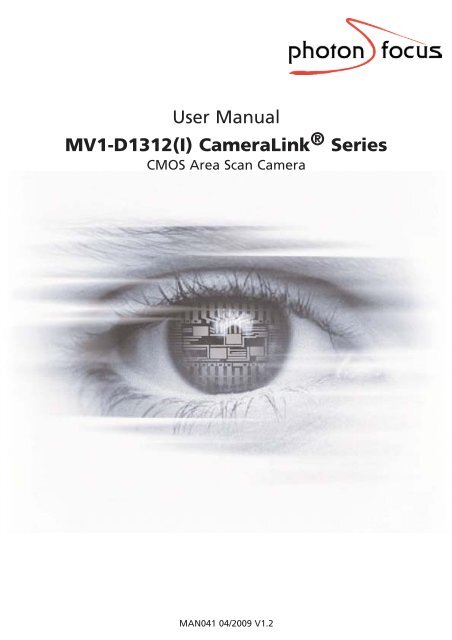
User Manual MV1-D1312(I) CameraLink®Series - Machine Vision
User Manual MV1-D1312(I) CameraLink®Series - Machine Vision
User Manual MV1-D1312(I) CameraLink®Series - Machine Vision

You also want an ePaper? Increase the reach of your titles
YUMPU automatically turns print PDFs into web optimized ePapers that Google loves.
<strong>User</strong> <strong>Manual</strong><strong>MV1</strong>-<strong>D1312</strong>(I) CameraLink ® SeriesCMOS Area Scan CameraMAN041 04/2009 V1.2
All information provided in this manual is believed to be accurate and reliable. Noresponsibility is assumed by Photonfocus AG for its use. Photonfocus AG reserves the right tomake changes to this information without notice.Reproduction of this manual in whole or in part, by any means, is prohibited without priorpermission having been obtained from Photonfocus AG.1
Contents1 Preface 71.1 About Photonfocus . . . . . . . . . . . . . . . . . . . . . . . . . . . . . . . . . . . . . . 71.2 Contact . . . . . . . . . . . . . . . . . . . . . . . . . . . . . . . . . . . . . . . . . . . . . 71.3 Sales Offices . . . . . . . . . . . . . . . . . . . . . . . . . . . . . . . . . . . . . . . . . . 71.4 Further information . . . . . . . . . . . . . . . . . . . . . . . . . . . . . . . . . . . . . . 71.5 Legend . . . . . . . . . . . . . . . . . . . . . . . . . . . . . . . . . . . . . . . . . . . . . 82 How to get started (CameraLink ® ) 93 Product Specification 133.1 Introduction . . . . . . . . . . . . . . . . . . . . . . . . . . . . . . . . . . . . . . . . . . 133.2 Feature Overview . . . . . . . . . . . . . . . . . . . . . . . . . . . . . . . . . . . . . . . 143.3 Technical Specification . . . . . . . . . . . . . . . . . . . . . . . . . . . . . . . . . . . . 153.4 Frame Grabber relevant Configuration . . . . . . . . . . . . . . . . . . . . . . . . . . . 184 Functionality 214.1 Image Acquisition . . . . . . . . . . . . . . . . . . . . . . . . . . . . . . . . . . . . . . . 214.1.1 Free-running and Trigger Mode . . . . . . . . . . . . . . . . . . . . . . . . . . . 214.1.2 Exposure Control . . . . . . . . . . . . . . . . . . . . . . . . . . . . . . . . . . . 234.1.3 Maximum Frame Rate . . . . . . . . . . . . . . . . . . . . . . . . . . . . . . . . 234.2 Pixel Response . . . . . . . . . . . . . . . . . . . . . . . . . . . . . . . . . . . . . . . . . 234.2.1 Linear Response . . . . . . . . . . . . . . . . . . . . . . . . . . . . . . . . . . . . 234.2.2 LinLog ® . . . . . . . . . . . . . . . . . . . . . . . . . . . . . . . . . . . . . . . . . 244.3 Test Images . . . . . . . . . . . . . . . . . . . . . . . . . . . . . . . . . . . . . . . . . . . 284.3.1 Ramp . . . . . . . . . . . . . . . . . . . . . . . . . . . . . . . . . . . . . . . . . . 284.3.2 LFSR . . . . . . . . . . . . . . . . . . . . . . . . . . . . . . . . . . . . . . . . . . . 284.3.3 Troubleshooting using the LFSR . . . . . . . . . . . . . . . . . . . . . . . . . . . 294.4 Image Correction . . . . . . . . . . . . . . . . . . . . . . . . . . . . . . . . . . . . . . . 314.4.1 Overview . . . . . . . . . . . . . . . . . . . . . . . . . . . . . . . . . . . . . . . . 314.4.2 Offset Correction (FPN, Hot Pixels) . . . . . . . . . . . . . . . . . . . . . . . . . 314.4.3 Gain Correction . . . . . . . . . . . . . . . . . . . . . . . . . . . . . . . . . . . . 334.4.4 Corrected Image . . . . . . . . . . . . . . . . . . . . . . . . . . . . . . . . . . . . 354.5 Reduction of Image Size . . . . . . . . . . . . . . . . . . . . . . . . . . . . . . . . . . . 364.5.1 Region of Interest (ROI) . . . . . . . . . . . . . . . . . . . . . . . . . . . . . . . 364.5.2 ROI configuration . . . . . . . . . . . . . . . . . . . . . . . . . . . . . . . . . . . 384.5.3 Calculation of the maximum frame rate (CameraLink ® ) . . . . . . . . . . . . . 394.6 External Trigger . . . . . . . . . . . . . . . . . . . . . . . . . . . . . . . . . . . . . . . . 414.6.1 Trigger Source . . . . . . . . . . . . . . . . . . . . . . . . . . . . . . . . . . . . . 414.7 Strobe Output . . . . . . . . . . . . . . . . . . . . . . . . . . . . . . . . . . . . . . . . . 414.8 Configuration Interface (CameraLink ® ) . . . . . . . . . . . . . . . . . . . . . . . . . . 414.9 Convolver (not available on <strong>MV1</strong>-<strong>D1312</strong>-160-CL) . . . . . . . . . . . . . . . . . . . . . 424.9.1 Functionality . . . . . . . . . . . . . . . . . . . . . . . . . . . . . . . . . . . . . . 42CONTENTS 3
CONTENTS4.9.2 Settings . . . . . . . . . . . . . . . . . . . . . . . . . . . . . . . . . . . . . . . . . 425 Hardware Interface 435.1 Connectors . . . . . . . . . . . . . . . . . . . . . . . . . . . . . . . . . . . . . . . . . . . 435.1.1 CameraLink ® Connector . . . . . . . . . . . . . . . . . . . . . . . . . . . . . . . 435.1.2 Power Supply . . . . . . . . . . . . . . . . . . . . . . . . . . . . . . . . . . . . . 435.1.3 Trigger and Strobe Signals . . . . . . . . . . . . . . . . . . . . . . . . . . . . . . 445.1.4 Status Indicator (CameraLink ® cameras) . . . . . . . . . . . . . . . . . . . . . . 455.2 CameraLink ® Data Interface . . . . . . . . . . . . . . . . . . . . . . . . . . . . . . . . . 455.3 Read-out Timing . . . . . . . . . . . . . . . . . . . . . . . . . . . . . . . . . . . . . . . . 475.3.1 Free running Mode . . . . . . . . . . . . . . . . . . . . . . . . . . . . . . . . . . 475.4 Trigger . . . . . . . . . . . . . . . . . . . . . . . . . . . . . . . . . . . . . . . . . . . . . 505.4.1 Trigger Modes . . . . . . . . . . . . . . . . . . . . . . . . . . . . . . . . . . . . . 505.4.2 Trigger Delay . . . . . . . . . . . . . . . . . . . . . . . . . . . . . . . . . . . . . . 506 The PFRemote Control Tool 536.1 Overview . . . . . . . . . . . . . . . . . . . . . . . . . . . . . . . . . . . . . . . . . . . . 536.2 PFRemote and PFLib . . . . . . . . . . . . . . . . . . . . . . . . . . . . . . . . . . . . . 536.3 Operating System . . . . . . . . . . . . . . . . . . . . . . . . . . . . . . . . . . . . . . . 536.4 Installation Notes . . . . . . . . . . . . . . . . . . . . . . . . . . . . . . . . . . . . . . . 536.5 Graphical <strong>User</strong> Interface (GUI) . . . . . . . . . . . . . . . . . . . . . . . . . . . . . . . . 546.5.1 Port Browser . . . . . . . . . . . . . . . . . . . . . . . . . . . . . . . . . . . . . . 546.5.2 Ports, Device Initialization . . . . . . . . . . . . . . . . . . . . . . . . . . . . . . 556.5.3 Main Buttons . . . . . . . . . . . . . . . . . . . . . . . . . . . . . . . . . . . . . 566.6 Device Properties . . . . . . . . . . . . . . . . . . . . . . . . . . . . . . . . . . . . . . . 567 Graphical <strong>User</strong> Interface (GUI) 577.1 <strong>MV1</strong>-<strong>D1312</strong>-160 . . . . . . . . . . . . . . . . . . . . . . . . . . . . . . . . . . . . . . . . 577.1.1 Exposure . . . . . . . . . . . . . . . . . . . . . . . . . . . . . . . . . . . . . . . . 587.1.2 Window . . . . . . . . . . . . . . . . . . . . . . . . . . . . . . . . . . . . . . . . 597.1.3 Trigger . . . . . . . . . . . . . . . . . . . . . . . . . . . . . . . . . . . . . . . . . 607.1.4 Data Output . . . . . . . . . . . . . . . . . . . . . . . . . . . . . . . . . . . . . . 617.1.5 Characteristics . . . . . . . . . . . . . . . . . . . . . . . . . . . . . . . . . . . . . 627.1.6 Correction . . . . . . . . . . . . . . . . . . . . . . . . . . . . . . . . . . . . . . . 637.1.7 Info . . . . . . . . . . . . . . . . . . . . . . . . . . . . . . . . . . . . . . . . . . . 657.2 <strong>MV1</strong>-<strong>D1312</strong>-40, <strong>MV1</strong>-<strong>D1312</strong>I-40, <strong>MV1</strong>-<strong>D1312</strong>-80, <strong>MV1</strong>-<strong>D1312</strong>I-80, <strong>MV1</strong>-<strong>D1312</strong>I-160 . 667.2.1 Exposure . . . . . . . . . . . . . . . . . . . . . . . . . . . . . . . . . . . . . . . . 677.2.2 Window . . . . . . . . . . . . . . . . . . . . . . . . . . . . . . . . . . . . . . . . 687.2.3 Trigger . . . . . . . . . . . . . . . . . . . . . . . . . . . . . . . . . . . . . . . . . 697.2.4 Data Output . . . . . . . . . . . . . . . . . . . . . . . . . . . . . . . . . . . . . . 707.2.5 Characteristics . . . . . . . . . . . . . . . . . . . . . . . . . . . . . . . . . . . . . 717.2.6 Convolver . . . . . . . . . . . . . . . . . . . . . . . . . . . . . . . . . . . . . . . . 727.2.7 Correction . . . . . . . . . . . . . . . . . . . . . . . . . . . . . . . . . . . . . . . 737.2.8 Info . . . . . . . . . . . . . . . . . . . . . . . . . . . . . . . . . . . . . . . . . . . 758 Mechanical and Optical Considerations 778.1 Mechanical Interface . . . . . . . . . . . . . . . . . . . . . . . . . . . . . . . . . . . . . 778.1.1 Cameras with CameraLink ® Interface . . . . . . . . . . . . . . . . . . . . . . . 778.2 Optical Interface . . . . . . . . . . . . . . . . . . . . . . . . . . . . . . . . . . . . . . . . 788.2.1 Cleaning the Sensor . . . . . . . . . . . . . . . . . . . . . . . . . . . . . . . . . . 788.3 Compliance . . . . . . . . . . . . . . . . . . . . . . . . . . . . . . . . . . . . . . . . . . . 804
CONTENTS6
Preface11.1 About PhotonfocusThe Swiss company Photonfocus is one of the leading specialists in the development of CMOSimage sensors and corresponding industrial cameras for machine vision, security & surveillanceand automotive markets.Photonfocus is dedicated to making the latest generation of CMOS technology commerciallyavailable. Active Pixel Sensor (APS) and global shutter technologies enable high speed andhigh dynamic range (120 dB) applications, while avoiding disadvantages like image lag,blooming and smear.Photonfocus has proven that the image quality of modern CMOS sensors is now appropriatefor demanding applications. Photonfocus’ product range is complemented by custom designsolutions in the area of camera electronics and CMOS image sensors.Photonfocus is ISO 9001 certified. All products are produced with the latest techniques in orderto ensure the highest degree of quality.1.2 ContactPhotonfocus AG, Bahnhofplatz 10, CH-8853 Lachen SZ, SwitzerlandSales Phone: +41 55 451 07 45 Email: sales@photonfocus.comSupport Phone: +41 55 451 01 37 Email: support@photonfocus.comTable 1.1: Photonfocus Contact1.3 Sales OfficesPhotonfocus products are available through an extensive international distribution networkand through our key account managers. Details of the distributor nearest you and contacts toour key account managers can be found at www.photonfocus.com.1.4 Further informationPhotonfocus reserves the right to make changes to its products and documentationwithout notice. Photonfocus products are neither intended nor certified foruse in life support systems or in other critical systems. The use of Photonfocusproducts in such applications is prohibited.Photonfocus is a trademark and LinLog ® is a registered trademark of PhotonfocusAG. CameraLink ® is a registered mark of the Automated Imaging Association.Product and company names mentioned herein are trademarks or trade namesof their respective companies.7
1 PrefaceReproduction of this manual in whole or in part, by any means, is prohibitedwithout prior permission having been obtained from Photonfocus AG.Photonfocus can not be held responsible for any technical or typographical errors.1.5 LegendIn this documentation the reader’s attention is drawn to the following icons:Important noteAlerts and additional informationAttention, critical warning✎Notification,user guide8
How to get started (CameraLink ® )21. Install a suitable frame grabber in your PC.To find a compliant frame grabber, please see the frame grabber compatibilitylist at www.photonfocus.com.2. Install the frame grabber software.✎Without installed frame grabber software the camera configuration tool PFRemotewill not be able to communicate with the camera. Please follow the instructionsof the frame grabber supplier.3. Remove the camera from its packaging. Please make sure the following items are includedwith your camera:• Power supply connector (7-pole power plug)• Camera body capIf any items are missing or damaged, please contact your dealership.4. Remove the camera body cap from the camera and mount a suitable lens.When removing the camera body cap or when changing the lens, the camerashould always be held with the opening facing downwards to prevent dust ordebris falling onto the CMOS sensor.Figure 2.1: Camera with protective cap and lens.Do not touch the sensor surface. Protect the image sensor from particles anddirt!9
2 How to get started (CameraLink ® )The sensor has no cover glass, therefore dust on the sensor surface may resembleto clusters or extended regions of dead pixel.To choose a lens, see the Lens Finder in the ’Support’ area atwww.photonfocus.com.5. Connect the camera to the frame grabber with a suitable CameraLink ® cable (see Fig. 2.2).CameraLink ® cables can be purchased from Photonfocus directly (www.photonfocus.com).Please note that Photonfocus provides appropriate solutions for your advanced visionapplications.Figure 2.2: Camera with frame grabber, power supply and cable.Do not connect or disconnect the CameraLink ® cable while camera power is on!For more information about CameraLink ® see Section 4.8.6. Connect a suitable power supply to the provided 7-pole power plug. For the connectorassembly see Fig. A.1. The pinout of the connector is shown in Appendix A.Check the correct supply voltage and polarity!operating voltage of +12V DC (± 10%).Do not exceed the maximum7. Connect the power supply to the camera (see Fig. 2.2).✎The status LED on the rear of the camera will light red for a short moment, andthen flash green. For more information see Section 5.1.4.10
8. Download the camera software PFRemote to your computer.You can find the latest version of PFRemote on the support page atwww.photonfocus.com.9. Install the camera software PFRemote. Please follow the instructions of the PFRemotesetup wizard.Figure 2.3: Screen shot PFremote setup wizard10. Start the camera software PFRemote and choose the communication port.Figure 2.4: PFRemote start window11. Check the status LED on the rear of the camera.✎The status LED lights green when an image is being produced, and it is red whenserial communication is active. For more information see Section 5.1.4.12. You may display images using the software that is provided by the frame grabbermanufacturer.11
2 How to get started (CameraLink ® )12
3.3 Technical SpecificationTechnical ParametersTechnologyScanning systemOptical format / diagonalResolution<strong>MV1</strong>-<strong>D1312</strong>(I) SeriesCMOS active pixel (APS)Progressive scan1” (13.6 mm diagonal) @ maximum resolution2/3” (11.6 mm diagonal) @ 1024 x 1024 resolution1312 x 1082 pixelsPixel size 8 µm x 8 µmActive optical area10.48 mm x 8.64 mm (maximum)Random noise < 0.3 DN @ 8 bit 1)Fixed pattern noise (FPN) 3.4 DN @ 8 bit / correction OFF 1)Fixed pattern noise (FPN) < 1DN @ 8 bit / correction ON 1)2)Dark current 0.65 fA / pixel @ 27 °CFull well capacity~ 100 ke −Spectral range <strong>MV1</strong>-<strong>D1312</strong> 350 nm ... 980 nm (see Fig. 3.2)Spectral range <strong>MV1</strong>-<strong>D1312</strong>I 350 nm ... 1100 nm (see Fig. 3.3)Responsivity <strong>MV1</strong>-<strong>D1312</strong>Responsivity <strong>MV1</strong>-<strong>D1312</strong>I210 x10 3 DN/(J/m 2 ) @ 625 nm / 8 bit300 x10 3 DN/(J/m 2 ) @ 850 nm / 8 bitQuantum Efficiency > 50 %Optical fill factor > 60 %Dynamic rangeColour formatUp to 120 dBMonochromeCharacteristic curve Linear, LinLog ®Shutter modeGreyscale resolutionGlobal shutter12 bit / 10 bit / 8 bitTable 3.2: General specification of the <strong>MV1</strong>-<strong>D1312</strong>(I) camera series (Footnotes: 1) Indicated values are typicalvalues. 2) Indicated values are subject to confirmation.)3.3 Technical Specification 15
3 Product Specification<strong>MV1</strong>-<strong>D1312</strong>(I)-40 <strong>MV1</strong>-<strong>D1312</strong>(I)-80 <strong>MV1</strong>-<strong>D1312</strong>(I)-160Exposure Time 10 µs ... 1.68 s 10 µs ... 1.68 s 10 µs ... 0.41 sExposure time increment 100 ns 50 ns 25 nsFrame rate 3) ( T int = 10 µs) 27 fps 54 fps 108 fpsPixel clock frequency 40 MHz 40 MHz 80 MHzPixel clock cycle 25 ns 25 ns 12.5 nsCamera taps 1 2 2Read out modesequential or simultaneousTable 3.3: Model-specific parameters (Footnote: 3) Maximum frame rate @ full resolution)<strong>MV1</strong>-<strong>D1312</strong>(I)-40 <strong>MV1</strong>-<strong>D1312</strong>(I)-80 <strong>MV1</strong>-<strong>D1312</strong>(I)-160Operating temperature 0°C ... 50°CCamera power supply +12 V DC (± 10 %)Trigger signal input range+5 .. +15 V DCMax. power consumption < 2.5 W < 3.0 W < 3.3 WLens mountC-Mount (CS-Mount optional)Dimensions 60 x 60 x 40 mm 3MassConformityTable 3.4: Physical characteristics and operating ranges265 gCE / RoHS / WEEFig. 3.2 shows the quantum efficiency and the responsivity of the A1312 CMOS sensor,displayed as a function of wavelength. For more information on photometric and radiometricmeasurements see the Photonfocus application notes AN006 and AN008 available in thesupport area of our website www.photonfocus.com.16
60%QEResponsivity120050%1000QuantumEfficiency40%30%20%800600400Responsivity [V V/J/m²]10%2000%0200 300 400 500 600 700 800 900 1000 1100Wavelength [nm]Figure 3.2: Spectral response of the A1312 CMOS image sensor (standard) in the <strong>MV1</strong>-<strong>D1312</strong> camera series(Hint: the red-shiftet curve corresponds to the responsivity curve.)Fig. 3.3 shows the quantum efficiency and the responsivity of the A1312I CMOS sensor,displayed as a function of wavelength..3.3 Technical Specification 17
3 Product Specification60%QEResponsivity120050%100040%QuantumEfficiency30%20%800600400Responsivity [V V/J/m²]10%2000%0200 300 400 500 600 700 800 900 1000 1100Wavelength [nm]Figure 3.3: Spectral response of the A1312I image sensor (NIR) in the <strong>MV1</strong>-<strong>D1312</strong>I camera series (Hint: thered-shiftet curve corresponds to the responsivity curve.)3.4 Frame Grabber relevant ConfigurationThe parameters and settings, which are essential to configure the frame grabber are shown inthe following table. The timing diagrams of the camera are given in Section 5.3.<strong>MV1</strong>-<strong>D1312</strong>(I)-40 <strong>MV1</strong>-<strong>D1312</strong>(I)-80 <strong>MV1</strong>-<strong>D1312</strong>(I)-160Pixel Clock per Tap 40 MHz 40 MHz 80 MHzNumber of Taps 1 2 2Greyscale resolution 12 bit / 10 bit / 8 bit 12 bit / 10 bit / 8 bit 12 bit / 10 bit / 8 bitLine pause 36 clock cycles 18 clock cycles 18 clock cyclesCC1 EXSYNC EXSYNC EXSYNCCC2 not used not used not usedCC3 not used not used not usedCC4 not used not used not usedTable 3.5: Summary of parameters needed for frame grabber configurationCameraLink ® port and bit assignments are compliant with the CameraLink ® standard (see [CL]).18
Bit Tap 0 Tap 0 Tap 08 Bit 10 Bit 12 Bit0 (LSB) A0 A0 A01 A1 A1 A12 A2 A2 A23 A3 A3 A34 A4 A4 A45 A5 A5 A56 A6 A6 A67 (MSB of 8 Bit) A7 A7 A78 - B0 B09 (MSB of 10 Bit) - B1 B110 - - B211 (MSB of 12 Bit) - - B3Table 3.6: CameraLink ® 1 Tap port and bit assignments for the <strong>MV1</strong>-<strong>D1312</strong>(I)-40 cameraBit Tap 0 Tap 1 Tap 0 Tap 1 Tap 0 Tap 18 Bit 8 Bit 10 Bit 10 Bit 12 Bit 12 Bit0 (LSB) A0 B0 A0 C0 A0 C01 A1 B1 A1 C1 A1 C12 A2 B2 A2 C2 A2 C23 A3 B3 A3 C3 A3 C34 A4 B4 A4 C4 A4 C45 A5 B5 A5 C5 A5 C56 A6 B6 A6 C6 A6 C67 (MSB of 8 Bit) A7 B7 A7 C7 A7 C78 - - B0 B4 B0 B49 (MSB of 10 Bit) - - B1 B5 B1 B510 - - - - B2 B611 (MSB of 12 Bit) - - - - B3 B7Table 3.7: CameraLink ® 2 Tap port and bit assignments for the <strong>MV1</strong>-<strong>D1312</strong>(I)-80 camera and for the <strong>MV1</strong>-<strong>D1312</strong>(I)-160 camera.3.4 Frame Grabber relevant Configuration 19
3 Product Specification20
AAFunctionality4This chapter serves as an overview of the camera configuration modes and explains camerafeatures. The goal is to describe what can be done with the camera. The setup of the<strong>MV1</strong>-<strong>D1312</strong>(I) series cameras is explained in later chapters.4.1 Image Acquisition4.1.1 Free-running and Trigger ModeThe <strong>MV1</strong>-<strong>D1312</strong>(I) CMOS cameras provide two different readout modes:Sequential readout Frame time is the sum of exposure time and readout time. Exposure timeof the next image can only start if the readout time of the current image is finished.Simultaneous readout (interleave) The frame time is determined by the maximum of theexposure time or of the readout time, which ever of both is the longer one. Exposuretime of the next image can start during the readout time of the current image.Sequential readoutSimultaneous readout<strong>MV1</strong>-<strong>D1312</strong>(I) SeriesavailableavailableTable 4.1: Readout mode of <strong>MV1</strong>-<strong>D1312</strong> Series cameraThe following figure illustrates the effect on the frame rate when using either the sequentialreadout mode or the simultaneous readout mode (interleave exposure).B F I H A = @ K J J E . H = A H = J A B F I 5 E K J = A K IH A = @ K J @ AB F I A N F I K H A J E 5 A G K A J E = H A = @ K J @ AB F I H A = @ K J J E A A N F I K H A J E A A N F I K H A J E A H A = @ K J J E A A N F I K H A J E A H A = @ K J J E AA N F I K H A J E A H A = @ K J J E A- N F I K H A J E AFigure 4.1: Frame rate in sequential readout mode and simultaneous readout modeSequential readout mode For the calculation of the frame rate only a single formula applies:frames per second equal to the invers of the sum of exposure time and readout time.21
4 FunctionalitySimultaneous readout mode (exposure time < readout time) The frame rate is given by thereadout time. Frames per second equal to the invers of the readout time.Simultaneous readout mode (exposure time > readout time) The frame rate is given by theexposure time. Frames per second equal to the invers of the exposure time.The simultaneous readout mode allows higher frame rate. However, if the exposure timestrongly exceeds the readout time, then the effect on the frame rate is neglectable.In simultaneous readout mode image output faces minor limitations. The overalllinear sensor reponse is partially restricted in the lower grey scale region.When changing readout mode from sequential to simultaneous readout modeor vice versa, new settings of the BlackLevelOffset and of the image correctionare required.Sequential readoutBy default the camera continuously delivers images as fast as possible ("Free-running mode")in the sequential readout mode. Exposure time of the next image can only start if the readouttime of the current image is finished.A N F I K H A H A = @ K J A N F I K H A H A = @ K JFigure 4.2: Timing in free-running sequential readout modeWhen the acquisition of an image needs to be synchronised to an external event, an externaltrigger can be used (refer to Section 4.6 and to Section 5.4). In this mode, the camera is idleuntil it gets a signal to capture an image.A N F I K H A H A = @ K J E @ A A N F I K H AA N J A H = J H E C C A HFigure 4.3: Timing in triggered sequential readout modeSimultaneous readout (interleave exposure)To achieve highest possible frame rates, the camera must be set to "Free-running mode" withsimultaneous readout. The camera continuously delivers images as fast as possible. Exposuretime of the next image can start during the readout time of the current image.A N F I K H A E @ A A N F I K H A E @ AH A = @ K J H A = @ K J B H = A J E AH A = @ K J Figure 4.4: Timing in free-running simultaneous readout mode (readout time> exposure time)22
A N F I K H A A N F I K H A A N F I K H A E @ AH A = @ K J E @ AH A = @ K J B H = A J E AFigure 4.5: Timing in free-running simultaneous readout mode (readout time< exposure time)When the acquisition of an image needs to be synchronised to an external event, an externaltrigger can be used (refer to Section 4.6 and to Section 5.4). In this mode, the camera is idleuntil it gets a signal to capture an image.Figure 4.6: Timing in triggered simultaneous readout mode4.1.2 Exposure ControlThe exposure time defines the period during which the image sensor integrates the incominglight. Refer to Table 3.3 for the allowed exposure time range.4.1.3 Maximum Frame RateThe maximum frame rate depends on the exposure time and the size of the image (see Section4.5.)4.2 Pixel Response4.2.1 Linear ResponseThe camera offers a linear response between input light signal and output grey level. This canbe modified by the use of LinLog ® as described in the following sections. In addition, a lineardigital gain may be applied, as follows. Please see Table 3.2 for more model-dependentinformation.Gain x1, x2, x4Gain x1, x2 and x4 are digital amplifications, which means that the digital image data aremultiplied in the camera by a factor 1, 2 or 4, respectively.4.2 Pixel Response 23
4 FunctionalityBlack Level AdjustmentThe black level is the average image value at no light intensity. It can be adjusted by thesoftware by changing the black level offset. Thus, the overall image gets brighter or darker.Use a histogram to control the settings of the black level.4.2.2 LinLog ®OverviewThe LinLog ® technology from Photonfocus allows a logarithmic compression of high lightintensities inside the pixel. In contrast to the classical non-integrating logarithmic pixel, theLinLog ® pixel is an integrating pixel with global shutter and the possibility to control thetransition between linear and logarithmic mode.In situations involving high intrascene contrast, a compression of the upper grey level regioncan be achieved with the LinLog ® technology. At low intensities each pixel shows a linearresponse. At high intensities the response changes to logarithmic compression (see Fig. 4.7).The transition region between linear and logarithmic response can be smoothly adjusted bysoftware and is continuously differentiable and monotonic./ H A O8 = K A E A = H 4 A I F I A5 = J K H = J E 9 A = ? F H A I I E 4 A I K J E C E C4 A I F I A5 J H C ? F H A I I E 8 = K A 8 = K A E C D J 1 J A I E J OFigure 4.7: Resulting LinLog2 response curveLinLog ® is controlled by up to 4 parameters (Time1, Time2, Value1 and Value2). Value1 and Value2correspond to the LinLog ® voltage that is applied to the sensor. The higher the parametersValue1 and Value2 respectively, the stronger the compression for the high light intensities. Time1and Time2 are normalised to the exposure time. They can be set to a maximum value of 1000,which corresponds to the exposure time.Examples in the following sections illustrate the LinLog ® feature.LinLog1In the simplest way the pixels are operated with a constant LinLog ® voltage which defines theknee point of the transition.This procedure has the drawback that the linear response curvechanges directly to a logarithmic curve leading to a poor grey resolution in the logarithmicregion (see Fig. 4.9).24
8 E CJ A N F8 = K A 8 = K AFigure 4.8: Constant LinLog voltage in the Linlog1 mode6 E A 6 E A = N JTypical LinLog1 Response Curve − Varying Parameter Value1300Time1=1000, Time2=1000, Value2=Value1Output grey level (8 bit) [DN]25020015010050V1 = 15V1 = 16V1 = 17V1 = 18V1 = 190Illumination IntensityFigure 4.9: Response curve for different LinLog settings in LinLog1 mode.4.2 Pixel Response 25
J4 FunctionalityLinLog2To get more grey resolution in the LinLog ® mode, the LinLog2 procedure was developed. InLinLog2 mode a switching between two different logarithmic compressions occurs during theexposure time (see Fig. 4.10). The exposure starts with strong compression with a highLinLog ® voltage (Value1). At Time1 the LinLog ® voltage is switched to a lower voltage resulting ina weaker compression. This procedure gives a LinLog ® response curve with more greyresolution. Fig. 4.11 and Fig. 4.12 show how the response curve is controlled by the threeparameters Value1, Value2 and the LinLog ® time Time1.Settings in LinLog2 mode, enable a fine tuning of the slope in the logarithmicregion.8 E CJ A N F8 = K A 8 = K A6 E A 6 E A 6 E A = N Figure 4.10: Voltage switching in the Linlog2 modeTypical LinLog2 Response Curve − Varying Parameter Time1300Time2=1000, Value1=19, Value2=14Output grey level (8 bit) [DN]25020015010050T1 = 840T1 = 920T1 = 960T1 = 980T1 = 9990Illumination IntensityFigure 4.11: Response curve for different LinLog settings in LinLog2 mode26
JTypical LinLog2 Response Curve − Varying Parameter Time1200Time2=1000, Value1=19, Value2=18Output grey level (8 bit) [DN]18016014012010080604020T1 = 880T1 = 900T1 = 920T1 = 940T1 = 960T1 = 980T1 = 10000Illumination IntensityFigure 4.12: Response curve for different LinLog settings in LinLog2 modeLinLog3To enable more flexibility the LinLog3 mode with 4 parameters was introduced. Fig. 4.13 showsthe timing diagram for the LinLog3 mode and the control parameters.8 E CJA N F8 = K A 8 = K A6 E A 6 E A6 E A 6 E A JA N F8 = K A ! + I J = J Figure 4.13: Voltage switching in the LinLog3 mode4.2 Pixel Response 27
4 Functionality300Typical LinLog2 Response Curve − Varying Parameter Time2Time1=850, Value1=19, Value2=18Output grey level (8 bit) [DN]25020015010050T2 = 950T2 = 960T2 = 970T2 = 980T2 = 9900Illumination IntensityFigure 4.14: Response curve for different LinLog settings in LinLog3 mode4.3 Test ImagesTest images are generated in the camera FPGA, independent of the image sensor. They can beused to check the transmission path from the camera to the frame grabber. Independent fromthe configured grey level resolution, every possible grey level appears the same number oftimes in a test image. Therefore, the histogram of the received image must be flat.A test image is a useful tool to find data transmission errors that are caused mostoften by a defective cable between camera and frame grabber.The analysis of the test images with a histogram tool gives the correct result atfull resolution only.4.3.1 RampDepending on the configured grey level resolution, the ramp test image outputs a constantpattern with increasing grey level from the left to the right side (see Fig. 4.15).4.3.2 LFSRThe LFSR (linear feedback shift register) test image outputs a constant pattern with apseudo-random grey level sequence containing every possible grey level that is repeated forevery row. The LFSR test pattern was chosen because it leads to a very high data toggling rate,which stresses the interface electronic and the cable connection.In the histogram you can see that the number of pixels of all grey values are the same.Please refer to application note [AN026] for the calculation and the values of the LFSR testimage.28
Figure 4.15: Ramp test images: 8 bit output (left), 10 bit output (right)Figure 4.16: LFSR (linear feedback shift register) test image4.3.3 Troubleshooting using the LFSRTo control the quality of your complete imaging system enable the LFSR mode and check thehistogram at full resolution. If your frame grabber application does not provide a real-timehistogram, store the image and use a graphic software tool to display the histogram.In the LFSR (linear feedback shift register) mode the camera generates a constantpseudo-random test pattern containing all grey levels. If the data transmission is error free, thehistogram of the received LFSR test pattern will be flat (Fig. 4.17). On the other hand, anon-flat histogram (Fig. 4.18) indicates problems, that may be caused either by the cable, bythe connectors or by the frame grabber.A possible origin of failure message can be caused by the CameraLink ® cablewhich exceeds the maximum length. Also, CameraLink ® cables may suffer eitherfrom stress due to wrong installation or from severe electromagnetic interference..4.3 Test Images 29
4 FunctionalitySome thinner CameraLink ® cables have a predefined direction. In these cablesnot all twisted pairs are separately shielded to meet the RS644 standard. Thesepairs are used for the transmission of the RX/TX and for the CC1 to CC4 lowfrequency control signals.Figure 4.17: LFSR test pattern received at the frame grabber and typical histogram for error-free datatransmissionFigure 4.18: LFSR test pattern received at the frame grabber and histogram containing transmission errorsCameraLink ® cables contain wire pairs, which are twisted in such a way that thecable impedance matches with the LVDS driver and receiver impedance. Excessstress on the cable results in transmission errors which causes distorted images.Therefore, please do not stretch and bend a CameraLink cable.In robots applications, the stress that is applied to the CameraLink ® cable is especially high dueto the fast movement of the robot arm. For such applications, special drag chain capable cablesare available. Please contact the Photonfocus Support for consulting expertise. AppropriateCameraLink ® cable solutions are available from Photonfocus..30
4.4 Image Correction4.4.1 OverviewThe camera possesses image pre-processing features, that compensate for non-uniformitiescaused by the sensor, the lens or the illumination. This method of improving the image qualityis generally known as ’Shading Correction’ or ’Flat Field Correction’ and consists of acombination of offset correction, gain correction and pixel interpolation.Since the correction is performed in hardware, there is no performance limitationof the cameras for high frame rates.The offset correction subtracts a configurable positive or negative value from the live imageand thus reduces the fixed pattern noise of the CMOS sensor. In addition, hot pixels can beremoved by interpolation. The gain correction can be used to flatten uneven illumination or tocompensate shading effects of a lens. Both offset and gain correction work on a pixel-per-pixelbasis, i.e. every pixel is corrected separately. For the correction, a black reference and a greyreference image are required. Then, the correction values are determined automatically in thecamera.Do not set any reference images when gain or LUT is enabled! Read the followingsections very carefully.Correction values of both reference images can be saved into the internal flash memory, butthis overwrites the factory presets. Then the reference images that are delivered by factorycannot be restored anymore.4.4.2 Offset Correction (FPN, Hot Pixels)The offset correction is based on a black reference image, which is taken at no illumination(e.g. lens aperture completely closed). The black reference image contains the fixed-patternnoise of the sensor, which can be subtracted from the live images in order to minimise thestatic noise.Offset correction algorithmAfter configuring the camera with a black reference image, the camera is ready to apply theoffset correction:1. Determine the average value of the black reference image.2. Subtract the black reference image from the average value.3. Mark pixels that have a grey level higher than 252 DN (@ 10 bit) as hot pixels.4. Store the result in the camera as the offset correction matrix.5. During image acquisition, subtract the correction matrix from the acquired image andinterpolate the hot pixels (see Section 4.4.2).4.4 Image Correction 31
!""""!""!!"4 Functionality" !! " = L A H = C A B > = ? H A B A H A ? AF E ? J K H A > = ? H A B A H A ? A E = C A B B I A J ? H H A ? J E = J H E NFigure 4.19: Schematic presentation of the offset correction algorithmHow to Obtain a Black Reference ImageIn order to improve the image quality, the black reference image must meet certain demands.• The black reference image must be obtained at no illumination, e.g. with lens apertureclosed or closed lens opening.• It may be necessary to adjust the black level offset of the camera. In the histogram of theblack reference image, ideally there are no grey levels at value 0 DN after adjustment ofthe black level offset. All pixels that are saturated black (0 DN) will not be properlycorrected (see Fig. 4.20). The peak in the histogram should be well below the hot pixelthreshold of 252 DN @ 10 bit.• Camera settings may influence the grey level. Therefore, for best results the camerasettings of the black reference image must be identical with the camera settings of theimage to be corrected.Figure 4.20: Histogram of a proper black reference image for offset correctionHot pixel correctionEvery pixel that exceeds a certain threshold in the black reference image is marked as a hotpixel. If the hot pixel correction is switched on, the camera replaces the value of a hot pixel byan average of its neighbour pixels (see Fig. 4.21).32
D J F E N A F F F F F F Figure 4.21: Hot pixel interpolation4.4.3 Gain CorrectionThe gain correction is based on a grey reference image, which is taken at uniform illuminationto give an image with a mid grey level.Gain correction is not a trivial feature. The quality of the grey reference imageis crucial for proper gain correction.Gain correction algorithmAfter configuring the camera with a black and grey reference image, the camera is ready toapply the gain correction:1. Determine the average value of the grey reference image.2. Subtract the offset correction matrix from the grey reference image.3. Divide the average value by the offset corrected grey reference image.4. Pixels that have a grey level higher than a certain threshold are marked as hot pixels.5. Store the result in the camera as the gain correction matrix.6. During image acquisition, multiply the gain correction matrix from the offset-correctedacquired image and interpolate the hot pixels (see Section 4.4.2).Gain correction is not a trivial feature. The quality of the grey reference imageis crucial for proper gain correction.4.4 Image Correction 33
!""%&'%'%"$!4 Functionality= L A H = C A B C H = OH A B A H A ? AF E ? J K H A" !% '' $ & ' & ! ' &C H = O H A B A H A ? AF E ? J K H A B B I A J ? H H A ? J E = J H E NC = E ? H H A ? J E = J H E NFigure 4.22: Schematic presentation of the gain correction algorithmGain correction always needs an offset correction matrix. Thus, the offset correctionalways has to be performed before the gain correction.How to Obtain a Grey Reference ImageIn order to improve the image quality, the grey reference image must meet certain demands.• The grey reference image must be obtained at uniform illumination.Use a high quality light source that delivers uniform illumination. Standard illuminationwill not be appropriate.• When looking at the histogram of the grey reference image, ideally there are no greylevels at full scale (1023 DN @ 10 bit). All pixels that are saturated white will not beproperly corrected (see Fig. 4.23).• Camera settings may influence the grey level. Therefore, the camera settings of the greyreference image must be identical with the camera settings of the image to be corrected.Figure 4.23: Proper grey reference image for gain correction34
!%""#$$$%#%"!!"!%""##$$##$"!!"4.4.4 Corrected ImageOffset, gain and hot pixel correction can be switched on separately. The followingconfigurations are possible:• No correction• Offset correction only• Offset and hot pixel correction• Hot pixel correction only• Offset and gain correction• Offset, gain and hot pixel correctionIn addition, the black reference image and grey reference image that are currently stored inthe camera RAM can be output." % !# $% " $ ' ' & & !" % !# "% " $? K H H A J E = C A B B I A J ? H H A ? J E = J H E NC = E ? H H A ? J E = J H E N? H H A ? J A @ E = C AFigure 4.24: Schematic presentation of the corrected image using gain correction algorithmTable 4.2 shows the minimum and maximum values of the correction matrices, i.e. the rangethat the offset and gain algorithm can correct.MinimumMaximumOffset correction -127 DN @ 10 bit +127 DN @ 10 bitGain correction 0.42 2.67Table 4.2: Offset and gain correction ranges4.4 Image Correction 35
4 Functionality4.5 Reduction of Image SizeWith Photonfocus cameras there are several possibilities to focus on the interesting parts of animage, thus reducing the data rate and increasing the frame rate. The most commonly usedfeature is Region of Interest (ROI).4.5.1 Region of Interest (ROI)Some applications do not need full image resolution (e.g. 1312 x 1082 pixels). By reducing theimage size to a certain region of interest (ROI), the frame rate can be drastically increased. Aregion of interest can be almost any rectangular window and is specified by its position withinthe full frame and its width (W) and height (H). Fig. 4.26 and Fig. 4.27 shows possibleconfigurations for the region of interest, and Table 4.3 presents numerical examples of howthe frame rate can be increased by reducing the ROI.Both reductions in x- and y-direction result in a higher frame rate.Any region of interest may NOT be placed outside of the center of the sensor. Examples shownin Fig. 4.25 illustrate configurations of the ROI that are NOT allowed.= > Figure 4.25: ROI configuration examples that are NOT allowedThe minimum width of the region of interest depends on the model of the <strong>MV1</strong>-<strong>D1312</strong>(I) camera series. For more details please consult Table 4.5 and Table 4.6.The minimum width must be positioned symmetrically towards the vertical centerline of the sensor as shown in Fig. 4.26 and Fig. 4.27). A list of possiblesettings of the ROI for each camera model is given in Table 4.6..36
" " F E N A " " F E N A @ K ! F E N A " " F E N A " " F E N A @ K ! F E N A = > Figure 4.26: Possible configuration of the region of interest for the <strong>MV1</strong>-<strong>D1312</strong>(I)-40 CMOS camera % F E N A % F E N A @ K ! F E N A % F E N A % F E N A @ K ! F E N A = > Figure 4.27: Possible configuration of the region of interest with <strong>MV1</strong>-<strong>D1312</strong>(I)-160 CMOS camera✎Itis recommended to re-adjust the settings of the shading correction each timea new region of interest is selected.4.5 Reduction of Image Size 37
4 FunctionalityROI Dimension [Standard] <strong>MV1</strong>-<strong>D1312</strong>(I)-40 <strong>MV1</strong>-<strong>D1312</strong>(I)-80 <strong>MV1</strong>-<strong>D1312</strong>(I)-1601312 x 1082 (full resolution) 27 fps 54 fps 108 fps288 x 1 (minimum resolution) 10245 fps 10863 fps not allowed ROI setting1280 x 1024 (SXGA) 29 fps 58 fps 117 fps1280 x 768 (WXGA) 39 fps 78 fps 156 fps800 x 600 (SVGA) 79 fps 157 fps 310 fps640 x 480 (VGA) 121 fps 241 fps 472 fps544 x 1 9615 fps 10498 fps 11022 fps544 x 1082 63 fps 125 fps 249 fps1312 x 544 54 fps 107 fps 214 fps1312 x 256 114 fps 227 fps 445 fps544 x 544 125 fps 248 fps 485 fps1024 x 1024 36 fps 72 fps 145 fps1312 x 1 8116 fps 9537 fps 10468 fpsTable 4.3: Frame rates of different ROI settings (exposure time 10 µs; correction on, and sequential readoutmode).Exposure time <strong>MV1</strong>-<strong>D1312</strong>(I)-40 <strong>MV1</strong>-<strong>D1312</strong>(I)-80 <strong>MV1</strong>-<strong>D1312</strong>(I)-16010 µs 27 / 27 fps 54 / 54 fps 108 / 108 fps100 µs 27 / 27 fps 54 / 54 fps 107 / 108 fps500 µs 27 / 27 fps 53 / 54 fps 103 / 108 fps1 ms 27 / 27 fps 51 / 54 fps 98 / 108 fps2 ms 26 / 27 fps 49 / 54 fps 89 / 108 fps5 ms 24 / 27 fps 42 / 54 fps 70 / 108 fps10 ms 22 / 27 fps 35 / 54 fps 52 / 99 fps12 ms 21 / 27 fps 33 / 54 fps 47 / 82 fpsTable 4.4: Frame rates of different exposure times, [sequential readout mode / simultaneous readoutmode], resolution 1312 x 1082 pixel (correction on).4.5.2 ROI configurationIn the <strong>MV1</strong>-<strong>D1312</strong>(I) camera series the following two restrictions have to be respected for theROI configuration:• The minimum width (w) of the ROI is camera model dependent, ranging from 288 pixel inthe <strong>MV1</strong>-<strong>D1312</strong>(I)-40 camera to 544 pixel in the <strong>MV1</strong>-<strong>D1312</strong>(I)-160 camera.• The region of interest must overlap a minimum number of pixels centered to the left andto the right of the vertical middle line of the sensor (ovl).38
For any camera model of the <strong>MV1</strong>-<strong>D1312</strong>(I) camera series the allowed ranges for the ROIsettings can be deduced by the following formula:x min = max(0, 656 + ovl − w)x max = min(656 − ovl, 1312 − w) .where "ovl" is the overlap over the middle line and "w" is the width of the region of interest.Any ROI settings exceeding the minimum ROI width must be modulo 32.<strong>MV1</strong>-<strong>D1312</strong>(I)-40 <strong>MV1</strong>-<strong>D1312</strong>(I)-80 <strong>MV1</strong>-<strong>D1312</strong>(I)-160ROI width (w) 288 ... 1312 416 ... 1312 544 ... 1312overlap (ovl) 144 208 272width condition modulo 32 modulo 32 modulo 32Table 4.5: Summary of the ROI configuration restrictions for the <strong>MV1</strong>-<strong>D1312</strong>(I) camera series indicating theminimum ROI width (w) and the required number of pixel overlap (ovl) over the sensor middle lineThe settings of the region of interest in x-direction are restricted to modulo 32(see Table 4.6).There are no restrictions for the settings of the region of interest in y-direction.4.5.3 Calculation of the maximum frame rate (CameraLink ® )The frame rate mainly depends on the exposure time and readout time. The frame rate is theinverse of the frame time.fps = 1t frameCalculation of the frame time (sequential mode)t frame ≥ t exp + t roCalculation of the frame time (simultaneous mode)The calculation of the frame time in simultaneous read out mode requires more detailed datainput and is skipped here for the purpose of clarity.✎The formula for the calculation of the frame time in simultaneous mode is availablefrom Photonfocus on request.4.5 Reduction of Image Size 39
4 FunctionalityWidth ROI-X (<strong>MV1</strong>-<strong>D1312</strong>(I)-40) ROI-X (<strong>MV1</strong>-<strong>D1312</strong>(I)-80) ROI-X (<strong>MV1</strong>-<strong>D1312</strong>(I)-160)288 512 not available not available320 480 ... 512 not available not available352 448 ... 512 not available not available384 416 ... 512 not available not available416 384 ... 512 448 not available448 352 ... 512 416 ... 448 not available480 320 ... 520 384 ... 448 not available512 288 ... 512 352 ... 448 not available544 256 ...512 320 ... 448 384576 224 ... 512 288 ... 448 352 ... 384608 192 ... 512 256 ... 448 320 ... 352640 160 ... 512 224 ... 448 288 ... 384672 128 ... 512 192 ... 448 256 ... 384704 96 ... 512 160 ... 448 224 ... 384736 64 ... 512 128 ... 448 192 ... 384768 32 ... 512 96 ... 448 160 ... 384800 0 ... 512 64 ... 448 128 ... 384832 0 ... 480 32 ... 448 96 ... 384864 0 ... 448 0 ... 448 64 ... 384896 0 ... 416 0 ... 416 32 ... 384... ... ... ...1312 0 0 0Table 4.6: Some possible ROI-X settingsROI Dimension <strong>MV1</strong>-<strong>D1312</strong>(I)-40 <strong>MV1</strong>-<strong>D1312</strong>(I)-80 <strong>MV1</strong>-<strong>D1312</strong>(I)-1601312 x 1082 t ro = 36.46 ms t ro = 18.23 ms t ro = 9.12 ms1024 x 512 t ro = 13.57 ms t ro = 6.78 ms t ro = 3.39 ms1024 x 256 t ro = 6.78 ms t ro = 3.39 ms t ro = 1.70 msTable 4.7: Read out time at different ROI settings for the <strong>MV1</strong>-<strong>D1312</strong>(I) CMOS camera series in sequentialread out mode.A frame rate calculator for calculating the maximum frame rate is available inthe support area of the Photonfocus website.40
4.6 External TriggerAn external trigger is an event that starts an exposure. The trigger signal is either generatedon the frame grabber (soft-trigger) or comes from an external device such as a light barrier. If atrigger signal is applied to the camera before the earliest time for the next trigger, this triggerwill be ignored.4.6.1 Trigger SourceThe trigger signal can be configured to be active high or active low. One of the followingtrigger sources can be used:Interface Trigger In the interface trigger mode, the trigger signal is applied to the camera bythe CameraLink ® interface.Trigger In the trigger mode, the trigger signal is applied directly to the camera by the powersupply connector (via an optocoupler).+ = A H =+ 1 J A H B = ? A 6 H E C C A H. H = A C H = > > A H 7 5 * D I J) O 6 H E C C A H5 K H ? A, ) 6 ) F J 1 F K J6 H E C C A H 1 F K J) O 6 H E C C A H5 K H ? AFigure 4.28: Trigger Inputs4.7 Strobe OutputThe strobe output is an opto-isolated output located on the power supply connector that canbe used to trigger a strobe. The strobe output can be used both in free-running and in triggermode. There is a programmable delay available to adjust the strobe pulse to your application.The strobe output needs a separate power supply.more information.Please see Section 5.4 for4.8 Configuration Interface (CameraLink ® )A CameraLink ® camera can be controlled by the user via a RS232 compatible asynchronousserial interface. This interface is contained within the CameraLink ® interface as shown in Fig.4.29 and is physically not directly accessible. Instead, the serial communication is usually routedthrough the frame grabber. For some frame grabbers it might be necessary to connect a serialcable from the frame grabber to the serial interface of the PC..4.6 External Trigger 41
4 Functionality+ = A H =1 = C A @ = J = . 8 ) 8 ) , 8 ) . H = A C H = > > A H+ = A H = E 2 E N A + ? + + 5 E C = I+ = A H = E 5 A H E = 1 J A H B = ? AFigure 4.29: CameraLink serial interface for camera communication4.9 Convolver (not available on <strong>MV1</strong>-<strong>D1312</strong>-160-CL)4.9.1 FunctionalityThe "Convolver" is a discrete 2D convolution filter with a 3x3 convolution kernel. The kernelcoefficients can be user-defined.The M x N discrete 2D convolution p out (x,y) of pixel p in (x,y) with convolution kernel h, scale sand offset o is defined in Fig. 4.30.Figure 4.30: Convolution formula4.9.2 SettingsThe following settings for the parameters are available:Offset Offset value o (see Fig. 4.30). Range: -4096 ... 4095Scale Scaling divisor s (see Fig. 4.30). Range: 1 ... 4095Coefficients Coefficients of convolution kernel h (see Fig. 4.30). Range: -4096 ... 4095.Assignment to coefficient properties is shown in Fig. 4.31.Figure 4.31: Convolution coefficients assignment42
Hardware Interface55.1 Connectors5.1.1 CameraLink ® ConnectorThe CameraLink ® cameras are interfaced to external components via• a CameraLink ® connector, which is defined by the CameraLink ® standard as a 26 pin, 0.5"Mini Delta-Ribbon (MDR) connector to transmit configuration, image data and trigger.• a subminiature connector for the power supply, 7-pin Binder series 712.The connectors are located on the back of the camera. Fig. 5.1 shows the plugs and the statusLED which indicates camera operation.Figure 5.1: Rear view of the CameraLink cameraThe CameraLink ® interface and connector are specified in [CL]. For further details including thepinout please refer to Appendix A. This connector is used to transmit configuration, imagedata and trigger signals.5.1.2 Power SupplyThe camera requires a single voltage input (see Table 3.4). The camera meets all performancespecifications using standard switching power supplies, although well-regulated linear powersupplies provide optimum performance.It is extremely important that you apply the appropriate voltages to your camera.Incorrect voltages will damage the camera.For further details including the pinout please refer to Appendix A..43
5 Hardware Interface5.1.3 Trigger and Strobe SignalsThe power connector contains an external trigger input and a strobe output.The trigger input is equipped with a constant current diode which limits thecurrent of the optocoupler over a wide range of voltages. Trigger signals canthus directly get connected with the input pin and there is no need for a currentlimiting resistor, that depends with its value on the input voltage. The inputvoltage to the TRIGGER pin must not exceed +15V DC, to avoid damage to theinternal ESD protection and the optocoupler!In order to use the strobe output, the internal optocoupler must be powered with 5 .. 15 V DC.The STROBE signal is an open-collector output, therefore, the user must connect a pull-upresistor (see Table 5.1) to STROBE_VDD (5 .. 15 V DC) as shown in Fig. 5.2. This resistor should belocated directly at the signal receiver.Figure 5.2: Circuit for the trigger input signalsThe maximum sink current of the STROBE pin is 8 mA. Do not connect inductiveor capacitive loads, such loads may result in damage of the optocoupler! If theapplication requires this, please use voltage suppressor diodes in parallel withthis components to protect the optocoupler.44
STROBE_VDD Pull-up Resistor15 V > 3.9 kOhm10 V > 2.7 kOhm8 V > 2.2 kOhm7 V > 1.8 kOhm5 V > 1.0 kOhmTable 5.1: Pull-up resistor for strobe output and different voltage levels5.1.4 Status Indicator (CameraLink ® cameras)A dual-color LED on the back of the camera gives information about the current status of theCameraLink ® cameras.LED GreenLED RedGreen when an image is output. At slow frame rates, the LED blinks with theFVAL signal. At high frame rates the LED changes to an apparently continuousgreen light, with intensity proportional to the ratio of readout time over frametime.Red indicates an active serial communication with the camera.Table 5.2: Meaning of the LED of the CameraLink ® cameras5.2 CameraLink ® Data InterfaceThe CameraLink ® standard contains signals for transferring the image data, controlinformation and the serial communication.Data signals: CameraLink ® data signals contain the image data. In addition, handshakingsignals such as FVAL, LVAL and DVAL are transmitted over the same physical channel.Camera control information: Camera control signals (CC-signals) can be defined by the cameramanufacturer to provide certain signals to the camera. There are 4 CC-signals availableand all are unidirectional with data flowing from the frame grabber to the camera. Forexample, the external trigger is provided by a CC-signal (see Table 5.3 for the CCassignment).CC1 EXSYNC External Trigger. May be generated either by the frame grabber itself(software trigger) or by an external event (hardware trigger).CC2 CTRL0 Control0. This signal is reserved for future purposes and is not used.CC3 CTRL1 Control1. This signal is reserved for future purposes and is not used.CC4 CTRL2 Control2. This signal is reserved for future purposes and is not used.Table 5.3: Summary of the Camera Control (CC) signals as used by PhotonfocusPixel clock: The pixel clock is generated on the camera and is provided to the frame grabberfor synchronisation.5.2 CameraLink ® Data Interface 45
5 Hardware InterfaceSerial communication: A CameraLink ® camera can be controlled by the user via a RS232compatible asynchronous serial interface. This interface is contained within theCameraLink ® interface and is physically not directly accessible. Refer to Section 4.8 formore information.+ = A H =1 = C A @ = J = . 8 ) 8 ) , 8 ) . H = A C H = > > A H+ = A H = E 2 E N A + ? + + 5 E C = I+ = A H = E 5 A H E = 1 J A H B = ? AFigure 5.3: 1-tap CameraLink systemThe frame grabber needs to be configured with the proper tap and resolution settings,otherwise the image will be distorted or not displayed with the correct aspect ratio. Refer toTable 3.3 and to Section 3.4 for a summary of frame grabber relevant specifications. Fig. 5.3shows symbolically a 1-tap system. For more information about taps refer to the relevantapplication note [AN021] on the Photonfocus website.46
5.3 Read-out Timing5.3.1 Free running ModeSequential readout timingBy default, the camera is in free running mode and delivers images without any externalcontrol signals. The sensor is operated in sequential readout mode, which means that thesensor is read out after the exposure time. Then the sensor is reset, a new exposure starts andthe readout of the image information begins again. The data is output on the rising edge ofthe pixel clock. The signals FRAME_VALID (FVAL) and LINE_VALID (LVAL) mask valid imageinformation. The signal SHUTTER indicates the active exposure period of the sensor and is shownfor clarity only.2 + 5 0 7 6 6 - 4. H = A 6 E A. 8 ) - N F I K H A6 E A+ 2 4 - E A F = K I A E A F = K I A E A F = K I A 8 ) . E H I J E A = I J E A, 8 ) , ) 6 )Figure 5.4: Timing diagram sequential readout modeSimultaneous readout timingTo achieve highest possible frame rates, the camera must be set to "Free-running mode" withsimultaneous readout. The camera continuously delivers images as fast as possible. Exposuretime of the next image can start during the readout time of the current image. The data isoutput on the rising edge of the pixel clock. The signals FRAME_VALID (FVAL) and LINE_VALID (LVAL)mask valid image information. The signal SHUTTER indicates the active integration phase of thesensor and is shown for clarity only.5.3 Read-out Timing 47
5 Hardware Interface2 + . H = A 6 E A5 0 7 6 6 - 4- N F I K H A6 E A- N F I K H A6 E A. 8 ) + 2 4 - E A F = K I A E A F = K I A E A F = K I A+ 2 4 - 8 ) . E H I J E A = I J E A, 8 ) , ) 6 )Figure 5.5: Timing diagram simultaneous readout mode (readout time > exposure time)2 + 5 0 7 6 6 - 4. H = A 6 E A- N F I K H A 6 E A. 8 ) + 2 4 - E A F = K I A E A F = K I A E A F = K I A+ 2 4 - 8 ) . E H I J E A = I J E A, 8 ) , ) 6 )Figure 5.6: Timing diagram simultaneous readout mode (readout time < exposure time)48
Frame timeExposure timePCLKSHUTTERFVAL (Frame Valid)LVAL (Line Valid)DVAL (Data Valid)DATALine pauseFrame time is the inverse of the frame rate.Period during which the pixels are integrating the incoming light.Pixel clock on CameraLink ® interface.Internal signal, shown only for clarity. Is ’high’ during the exposuretime.Is ’high’ while the data of one complete frame are transferred.Is ’high’ while the data of one line are transferred. Example: To transferan image with 640x480 pixels, there are 480 LVAL within one FVAL activehigh period. One LVAL lasts 640 pixel clock cycles.Is ’high’ while data are valid.Transferred pixel values. Example: For a 100x100 pixel image, there are100 values transferred within one LVAL active high period, or 100*100values within one FVAL period.Delay before the first line and after every following line when readingout the image data.Table 5.4: Explanation of control and data signals used in the timing diagramThese terms will be used also in the timing diagrams of Section 5.4.5.3 Read-out Timing 49
5 Hardware Interface5.4 Trigger5.4.1 Trigger ModesThe following sections show the timing diagram for the trigger modes. The signal ExSyncdenotes the trigger signal that is provided either by the interface trigger or the I/O trigger (seeSection 4.6). The other signals are explained in Table 5.4. For an active high trigger signal, theimage acquisition begins with the rising edge of the trigger signal. The image is read out afterthe pre-configured exposure time. After the readout, the sensor returns to the reset state andthe camera waits for a new trigger pulse (see Fig. 5.7).The data is output on the rising edge of the pixel clock, the handshaking signals FRAME_VALID(FVAL) and LINE_VALID (LVAL) mask valid image information. The signal SHUTTER in Fig. 5.7indicates the active integration phase of the sensor and is shown for clarity only.2 + - : 5 ; +5 0 7 6 6 - 4. H = A 6 E A- N F I K H A6 E A. 8 ) + 2 4 - E A F = K I A E A F = K I A E A F = K I A 8 ) . E H I J E A = I J E A, 8 ) , ) 6 )Figure 5.7: Trigger timing diagram for camera controlled exposure5.4.2 Trigger DelayThe total delay between the trigger edge and the camera exposure consists of the delay in theframe grabber and the camera (Fig. 5.8). Usually, the delay in the frame grabber is relativelylarge to avoid accidental triggers caused by voltage spikes (see Fig. 5.9)..50
!""!+ = A H = + = A H = E . H = A / H = > > A H1 J A H B = ? A 6 H E C C A H, ) 6 )+ + F J 1 2 4 6 )6 H E C C A H 5 K H ? A1 6 H E C C A H2 4 6 *6 H E C C A H 5 K H ? A6 H E C C A H1 + J H 1 * = H @Figure 5.8: Trigger Delay visualisation from the trigger source to the cameraJ @ . /6 4 1 / / - 46 H E C C A H I K H ? AJ E J J A H- : 5 ; +1 J - : 5 ; +. H = A C H = > > A H+ = A H =J @ ? = A H =5 0 7 6 6 - 4+ = A H =J @ F J 1 J @ ? = A H =+ = A H = F J 1 + = A H =Figure 5.9: Timing Diagram for Trigger Delay.5.4 Trigger 51
5 Hardware InterfaceFor the delay in the frame grabber, please ask your frame grabber manufacturer. The cameradelay consists of a constant trigger delay and a variable delay (jitter), due to the sampling ofthe trigger signal by the clocked camera electronic. The trigger delay and the jitter arespecified in Table 5.6 and shown in Fig. 5.9. The description of the parameters is summarized inTable 5.5.Trigger delay typet d−FGt jittert d−camerat d−optoDescriptionTrigger delay of the frame grabber, refer to frame grabber manualVariable camera trigger delayConstant camera trigger delayVariable trigger delay of opto couplerTable 5.5: Trigger Delay ParametersTrigger delay type <strong>MV1</strong>-<strong>D1312</strong>(I)-40 <strong>MV1</strong>-<strong>D1312</strong>(I)-80 <strong>MV1</strong>-<strong>D1312</strong>(I)-160t jitter 100 ns 50 ns 25 nst d−camera 600 ns 300 ns 150 nsTable 5.6: Trigger Delay for the <strong>MV1</strong>-<strong>D1312</strong>(I) camera series in sequential read out modeDelay type<strong>MV1</strong>-<strong>D1312</strong>(I) SeriesTrigger t d−opto90 nsStrobe t d−opto (min/max) (0.2 / 1.4) µsTable 5.7: Interface Strobe/Trigger Delay for the <strong>MV1</strong>-<strong>D1312</strong>(I) camera seriesIn simultaneous read out mode trigger delay times may exceed indicated triggerdelay times of the sequential read out mode (see Table 5.6).Trigger multiple cameras with strobe output only with an additional buffer.✎Pleasecontact Photonfocus for further information on trigger delay times insimultaneous read out mode..52
The PFRemote Control Tool66.1 OverviewPFRemote is a graphical configuration tool for Photonfocus cameras. The latest release can bedownloaded from the support area of www.photonfocus.com.All Photonfocus cameras can be either configured by PFRemote, or they can be programmedwith custom software using the PFLib SDK ([PFLIB]).6.2 PFRemote and PFLibAs shown in Fig. 6.1, the camera parameters can be controlled by PFRemote and PFLibrespectively. To grab an image use the software or the SDK that was delivered with your framegrabber.Figure 6.1: PFRemote and PFLib in context with the CameraLink frame grabber software6.3 Operating SystemThe PFRemote GUI is available for Windows OS only. For Linux or QNX operating systems, weprovide the necessary libraries to control the camera on request, but there is no graphical userinterface available.If you require support for Linux or QNX operating systems, you may contact usfor details of support conditions.6.4 Installation NotesBefore installing the required software with the PFInstaller, make sure that your frame grabbersoftware is installed correctly.Several DLLs are necessary in order to be able to communicate with the cameras:53
6 The PFRemote Control Tool• PFCAM.DLL: The main DLL file that handles camera detection, switching to specific cameraDLL and provides the interface for the SDK.• ’CAMERANAME’.DLL: Specific camera DLL, e.g. mv_d1024e_3d01_160.dll.• COMDLL.DLL: Communication DLL. This COMDLL is not necessarily CameraLink ® specific, butmay depend on a CameraLink ® API compatible DLL, which should also be provided byyour frame grabber manufacturer.• CLALLSERIAL.DLL: Interface to CameraLink ® frame grabber which supports the clallserial.dll.• CLSER_USB.DLL: Interface to USB port.More information about these DLLs is available in the SDK documentation [SW002].6.5 Graphical <strong>User</strong> Interface (GUI)PFRemote consists of a main window (Fig. 6.2) and a configuration dialog. In the main window,the camera port can be opened or closed, and log messages are displayed at the bottom. Theconfiguration dialog appears as a sub window as soon as a camera port was openedsuccessfully. In the sub window of PFRemote the user can configure the camera properties.The following sections describe the general structure of PFRemote.6.5.1 Port BrowserOn start, PFRemote displays a list of available communication ports in the main window.Figure 6.2: PFRemote main window with PortBrowser and log messagesTo open a camera on a specific port double click on the port name (e.g. USB). Alternativelyright click on the port name and choose Open & Configure.... The port is then queried for acompatible Photonfocus camera.In the PFRemote main window, there are two menus with the following entries available:File MenuClear Log: Clears the log file bufferQuit: Exit the programHelp MenuAbout: Copyright notice and version informationHelp F1: Invoke the online help (PFRemote documentation)54
6.5.2 Ports, Device InitializationAfter starting PFRemote, the main window as shown in Fig. 6.2 will appear. In the PortBrowserin the upper left corner you will see a list of supported ports.Depending on the configuration, your port names may differ, and not every portmay be functional.If your frame grabber supports clallserial.dll version 1.1 ( CameraLink ® compliantstandard Oct 2001), the name of the manufacturer is shown in the PortBrowser.If your frame grabber supports clallserial.dll version 1.0 (CameraLink ® compliantstandard Oct 2000), the PortBrowser shows either the name of the dll or themanufacturer name or displays "Unknown".If your frame grabber does not support clallserial.dll, copy the clserXXXX.dll ofyour frame grabber in the PFRemote directory and rename it to clser.dll. ThePortBrowser will then indicate this DLL as "clser.dll at PFRemote directory".After connecting the camera, the device can be opened with a double click on the port nameor by right-clicking on the port name and choosing Open & Configure. If the initialisation ofthe camera was successful, the configuration dialog will open. The device is closed whenPFRemote is closed. Alternatively, e.g. when connecting another camera or evaluation kit, thedevice can also be closed explicitely by right clicking on the port name and choosing Close.Make sure that the configuration dialog is closed prior to closing the port.✎Errors, warnings or other important activities are logged in a log window at thebottom of the main window.If the device does not open, check the following:• Is the power LED of the camera active? Do you get an image in the display software ofyour frame grabber?• Verify all cable connections and the power supply.• Check the communication LED of the camera: do you see some activity when you try toaccess the camera?6.5 Graphical <strong>User</strong> Interface (GUI) 55
6 The PFRemote Control Tool6.5.3 Main ButtonsThe buttons on the right side of the configuration dialog store and reset the cameraconfiguration.Figure 6.3: Main buttonsReset: Reset the camera and load the default configuration.Store as defaults: Store the current configuration in the camera flash memory as the defaultconfiguration. After a reset, the camera will load this configuration by default.Settings file - File Load: Load a stored configuration from a file.Settings file - File Save: Save current configuration to a file.Factory Reset: Reset camera and reset the configuration to the factory defaults.6.6 Device PropertiesCameras or sensor devices are generally addressed as ’device’ in this software. These deviceshave properties that are accessed by a property name. These property names are translatedinto register accesses on the driver DLL. The property names are reflected in the GUI as far aspracticable. A property name normally has a special mark up throughout this document, forexample: ExposureTime. Some properties are grouped into a structure whose member isaccessed via dot notation, e.g. Window.X (for the start X value of a region of interest). Whenchanging a property, the property name can always be seen in the log window of the mainprogram window.56
Graphical <strong>User</strong> Interface (GUI)77.1 <strong>MV1</strong>-<strong>D1312</strong>-160This section describes the parameters of the following camera:• <strong>MV1</strong>-<strong>D1312</strong>-160-CL, CameraLink interfaceThe following sections are grouped according to the tabs in the configuration dialog.Figure 7.1: <strong>MV1</strong>-<strong>D1312</strong>-160 frame rate and average valueFrame Rate [fps :] Shows the actual frame rate of the camera in frames per second.Update: To update the value of the frame rate, click on this button.Average Value: Greyscale average of the actual image. This value is in 12bit (0...4095).Update: To update the value of the average, click on this button.57
7 Graphical <strong>User</strong> Interface (GUI)7.1.1 ExposureThis tab contains exposure settings.Figure 7.2: <strong>MV1</strong>-<strong>D1312</strong>-160 exposure panelExposureExposure time [ms :] Configure the exposure time in milliseconds.58
7.1.2 WindowThis tab contains the settings for the region of interest.Figure 7.3: <strong>MV1</strong>-<strong>D1312</strong>-160 window panelRegion of InterestThe region of interest (ROI) is defined as a rectangle (X, Y), (W, H) whereX: X - coordinate, starting from 0 in the upper left corner.Y: Y - coordinate, starting from 0 in the upper left corner.W: Window width (in steps of 32 pixel).H: Window height.Set to max ROI: Set Window to maximal ROI (X=0; Y=0; W=1312; H=1082).Window width is only available in steps of 32 pixel.7.1 <strong>MV1</strong>-<strong>D1312</strong>-160 59
7 Graphical <strong>User</strong> Interface (GUI)7.1.3 TriggerThis tab contains trigger and strobe settings.Figure 7.4: <strong>MV1</strong>-<strong>D1312</strong>-160 trigger panelTriggerTrigger Source:Free running: The camera continuously delivers images with a certain configurable frame rate.Interface Trigger: The Trigger signal is applied to the camera by the CameraLink frame grabberor the USB interface respectively.I/O Trigger: The trigger signal is applied directly to the camera on the power supply connector.Further trigger settings:Trigger signal active low: Define the trigger signal to be active high (default) or active low.StrobeThe camera generates a strobe output signal that can be used to trigger a strobe. The pulsewidth can be defined by software. To turn off strobe output, set StrobePulseWidth to 0.Strobe Pulse Width [ms :] The pulse width of the strobe trigger in milliseconds.60
7.1.4 Data OutputThis tab contains image data settings.Figure 7.5: <strong>MV1</strong>-<strong>D1312</strong>-160 data output panelOutput ModeOutput Mode:Normal: Normal mode.LFSR: Test image. Linear feedback shift register (pseudo-random image). The pattern dependson the grey level resolution.Ramp: Test image. Values of pixel are incremented by 1, starting at each row. The patterndepends on the grey level resolution.Resolution:8 Bit: Grey level resolution of 8 bit.10 Bit: Grey level resolution of 10 bit.12 Bit: Grey level resolution of 12 bit.Digital Gain:1x: No digital gain, normal mode.2x: Digital gain 2.4x: Digital gain 4.Digital Offset: Substracts an offset from the data. Only available in gain mode.7.1 <strong>MV1</strong>-<strong>D1312</strong>-160 61
7 Graphical <strong>User</strong> Interface (GUI)7.1.5 CharacteristicsThis tab contains LinLog and Skimming settings.Figure 7.6: <strong>MV1</strong>-<strong>D1312</strong>-160 characteristics panelLinLogThe LinLog technology from Photonfocus allows a logarithmic compression of high lightintensities. In contrast to the classical non-integrating logarithmic pixel, the LinLog pixel is anintegrating pixel with global shutter and the possibility to control the transition betweenlinear and logarithmic mode (Section 4.2.2). There are 3 predefined LinLog settings available.Alternatively, custom settings can be defined in the <strong>User</strong> defined Mode.LinLog Mode: Off: LinLog is disabled. Low/Normal/High compression: Three LinLogpresettings. <strong>User</strong> defined: Value1, Time1, Value2 and Time2. The Linlog times are perthousand of the exposure time. Time 800 means 80% of the exposure time.Black Level OffsetIt may be necessary to adjust the black level offset of the camera.Black Level Offset: Black level offset value. Use this to adjust the black level.Simultaneous readout (Interleave)The simultaneous readout mode allows higher frame rate.Simultaneous readout (Interleave): Enable the simultaneous readout mode.62
7.1.6 CorrectionThis tab contains correction settings.Figure 7.7: <strong>MV1</strong>-<strong>D1312</strong>-160 correction panelCorrection ModeThis camera has image pre-processing features, that compensate for non-uniformities causedby the sensor, the lens or the illumination.Off: No correction.Offset: Activate offset correctionOffset + Hotpixel: Activate offset and hot pixel correction.Hotpixel: Activate hot pixel correction.Offset + Gain: Activate offset and gain correction.Offset + Gain + Hotpixel: Activate offset, gain and hot pixel correction.CalibrationOffset (FPN), Hotpixel Correction: The offset correction is based on a black reference image,which is taken at no illumination (e.g. lens aperture completely closed). The blackreference image contains the fixed-pattern noise of the sensor, which can be subtractedfrom the live images in order to minimize the static noise. Close the lens of the camera.Click on the Validation button. If the Set Black Ref - button is still inactive, the average ofthe image is out of range. Change to panel Charateristics and change the PropertyBlackLevelOffset until the average of the image is between 160 and 400DN. Click againon the Validation button and then on the Set Black Ref Button.If only offset and hot pixel correction is needed it is not necessary to calibrate agrey image. (see Calculate)7.1 <strong>MV1</strong>-<strong>D1312</strong>-160 63
7 Graphical <strong>User</strong> Interface (GUI)Gain Correction: The gain correction is based on a grey reference image, which is taken atuniform illumination to give an image with a mid grey level.Gain correction is not a trivial feature. The quality of the grey reference imageis crucial for proper gain correction.Produce a grey image with an average between 2200 and 3600DN. Click on the Validationbutton to check the average. If the average is in range, the Set Grey Ref button is active.Calculate: Calculate the correction values into the camera RAM. To make the correction valuespermanent, use the ’Save to Flash’ button.Save to Flash: Save the current correction values to the internal flash memory.This will overwrite the factory presets.64
7.1.7 InfoThis panel shows camera specific information such as type code, serial number and firmwarerevision of the FPGA and microcontroller and the description of the camera interface.Figure 7.8: <strong>MV1</strong>-<strong>D1312</strong>-160 info panelTypecode: Type code of the connected camera.Serial: Serial number of the connected camera.FPGA Sensor Revision: Firmware revision of built-in Sensor FPGA of the connected camera.uC Revision: Firmware revision of built-in microcontroller of the connected camera.Interface: Description of the camera interface.For any support requests, please enclose the information provided on this tab.7.1 <strong>MV1</strong>-<strong>D1312</strong>-160 65
7 Graphical <strong>User</strong> Interface (GUI)7.2 <strong>MV1</strong>-<strong>D1312</strong>-40, <strong>MV1</strong>-<strong>D1312</strong>I-40, <strong>MV1</strong>-<strong>D1312</strong>-80, <strong>MV1</strong>-<strong>D1312</strong>I-80,<strong>MV1</strong>-<strong>D1312</strong>I-160This section describes the parameters of the following cameras:• <strong>MV1</strong>-<strong>D1312</strong>-40-CL, CameraLink interface,• <strong>MV1</strong>-<strong>D1312</strong>I-40-CL, CameraLink interface,• <strong>MV1</strong>-<strong>D1312</strong>-80-CL, CameraLink interface,• <strong>MV1</strong>-<strong>D1312</strong>I-80-CL, CameraLink interface,• <strong>MV1</strong>-<strong>D1312</strong>I-160-CL, CameraLink interface.The following sections are grouped according to the tabs in the configuration dialog.Figure 7.9: <strong>MV1</strong>-<strong>D1312</strong>-40 frame rate and average valueFrame Rate [fps :] Shows the actual frame rate of the camera in frames per second.Update: To update the value of the frame rate, click on this button.Average Value: Greyscale average of the actual image. This value is in 12bit (0...4095).Update: To update the value of the average, click on this button.66
7.2.1 ExposureThis tab contains exposure settings.Figure 7.10: <strong>MV1</strong>-<strong>D1312</strong>-40 exposure panelExposureExposure time [ms :] Configure the exposure time in milliseconds.7.2 <strong>MV1</strong>-<strong>D1312</strong>-40, <strong>MV1</strong>-<strong>D1312</strong>I-40, <strong>MV1</strong>-<strong>D1312</strong>-80, <strong>MV1</strong>-<strong>D1312</strong>I-80, <strong>MV1</strong>-<strong>D1312</strong>I-160 67
7 Graphical <strong>User</strong> Interface (GUI)7.2.2 WindowThis tab contains the settings for the region of interest.Figure 7.11: <strong>MV1</strong>-<strong>D1312</strong>-40 window panelRegion of InterestThe region of interest (ROI) is defined as a rectangle (X, Y), (W, H) whereX: X - coordinate, starting from 0 in the upper left corner.Y: Y - coordinate, starting from 0 in the upper left corner.W: Window width (in steps of 32 pixel).H: Window height.Set to max ROI: Set Window to maximal ROI (X=0; Y=0; W=1312; H=1082).Window width is only available in steps of 32 pixel.68
7.2.3 TriggerThis tab contains trigger and strobe settings.Figure 7.12: <strong>MV1</strong>-<strong>D1312</strong>-40 trigger panelTriggerTrigger Source:Free running: The camera continuously delivers images with a certain configurable frame rate.Interface Trigger: The Trigger signal is applied to the camera by the CameraLink frame grabberor the USB interface respectively.I/O Trigger: The trigger signal is applied directly to the camera on the power supply connector.Further trigger settings:Trigger signal active low: Define the trigger signal to be active high (default) or active low.StrobeThe camera generates a strobe output signal that can be used to trigger a strobe. The pulsewidth can be defined by software. To turn off strobe output, set StrobePulseWidth to 0.Strobe Pulse Width [ms :] The pulse width of the strobe trigger in milliseconds.7.2 <strong>MV1</strong>-<strong>D1312</strong>-40, <strong>MV1</strong>-<strong>D1312</strong>I-40, <strong>MV1</strong>-<strong>D1312</strong>-80, <strong>MV1</strong>-<strong>D1312</strong>I-80, <strong>MV1</strong>-<strong>D1312</strong>I-160 69
7 Graphical <strong>User</strong> Interface (GUI)7.2.4 Data OutputThis tab contains image data settings.Figure 7.13: <strong>MV1</strong>-<strong>D1312</strong>-40 data output panelOutput ModeOutput Mode:Normal: Normal mode.LFSR: Test image. Linear feedback shift register (pseudo-random image). The pattern dependson the grey level resolution.Ramp: Test image. Values of pixel are incremented by 1, starting at each row. The patterndepends on the grey level resolution.Resolution:8 Bit: Grey level resolution of 8 bit.10 Bit: Grey level resolution of 10 bit.12 Bit: Grey level resolution of 12 bit.Digital Gain:1x: No digital gain, normal mode.2x: Digital gain 2.4x: Digital gain 4.Digital Offset: Substracts an offset from the data. Only available in Gain Mode.70
7.2.5 CharacteristicsThis tab contains LinLog and Skimming settings.Figure 7.14: <strong>MV1</strong>-<strong>D1312</strong>-40 characteristics panelLinLogThe LinLog technology from Photonfocus allows a logarithmic compression of high lightintensities. In contrast to the classical non-integrating logarithmic pixel, the LinLog pixel is anintegrating pixel with global shutter and the possibility to control the transition betweenlinear and logarithmic mode (Section 4.2.2). There are 3 predefined LinLog settings available.Alternatively, custom settings can be defined in the <strong>User</strong> defined Mode.LinLog Mode: Off: LinLog is disabled. Low/Normal/High compression: Three LinLogpresettings. <strong>User</strong> defined: Value1, Time1, Value2 and Time2. The Linlog times are perthousand of the exposure time. Time 800 means 80% of the exposure time.Black Level OffsetIt may be necessary to adjust the black level offset of the camera.Black Level Offset: Black level offset value. Use this to adjust the black level.Simultaneous readout (Interleave)The simultaneous readout mode allows higher frame rate.Simultaneous readout (Interleave): Enable the simultaneous readout mode.7.2 <strong>MV1</strong>-<strong>D1312</strong>-40, <strong>MV1</strong>-<strong>D1312</strong>I-40, <strong>MV1</strong>-<strong>D1312</strong>-80, <strong>MV1</strong>-<strong>D1312</strong>I-80, <strong>MV1</strong>-<strong>D1312</strong>I-160 71
7 Graphical <strong>User</strong> Interface (GUI)7.2.6 ConvolverThis tab contains the Convolver settings.Figure 7.15: <strong>MV1</strong>-<strong>D1312</strong>-40 convolver panelOffsetOffset: Offset value o. Range: -4096 ... 4095.ScaleScale: Scale value s. Range: 1 ... 4095.CoefficientsCoefficents: Coefficients of the convolution kernel h. Range: -4096 ... 4095.72
7.2.7 CorrectionThis tab contains correction settings.Figure 7.16: <strong>MV1</strong>-<strong>D1312</strong>-40 correction panelCorrection ModeThis camera has image pre-processing features, that compensate for non-uniformities causedby the sensor, the lens or the illumination.Off: No correction.Offset: Activate offset correctionOffset + Hotpixel: Activate offset and hot pixel correction.Hotpixel: Activate hot pixel correction.Offset + Gain: Activate offset and gain correction.Offset + Gain + Hotpixel: Activate offset, gain and hot pixel correction.CalibrationOffset (FPN), Hotpixel Correction: The offset correction is based on a black reference image,which is taken at no illumination (e.g. lens aperture completely closed). The blackreference image contains the fixed-pattern noise of the sensor, which can be subtractedfrom the live images in order to minimize the static noise. Close the lens of the camera.Click on the Validation button. If the Set Black Ref - button is still inactive, the average ofthe image is out of range. Change to panel Charateristics and change the PropertyBlackLevelOffset until the average of the image is between 160 and 400DN. Click againon the Validation button and then on the Set Black Ref Button.7.2 <strong>MV1</strong>-<strong>D1312</strong>-40, <strong>MV1</strong>-<strong>D1312</strong>I-40, <strong>MV1</strong>-<strong>D1312</strong>-80, <strong>MV1</strong>-<strong>D1312</strong>I-80, <strong>MV1</strong>-<strong>D1312</strong>I-160 73
7 Graphical <strong>User</strong> Interface (GUI)If only offset and hot pixel correction is needed it is not necessary to calibrate agrey image. (see Calculate)Gain Correction: The gain correction is based on a grey reference image, which is taken atuniform illumination to give an image with a mid grey level.Gain correction is not a trivial feature. The quality of the grey reference imageis crucial for proper gain correction.Produce a grey image with an average between 2200 and 3600DN. Click on the Validationbutton to check the average. If the average is in range, the Set Grey Ref button is active.Calculate: Calculate the correction values into the camera RAM. To make the correction valuespermanent, use the ’Save to Flash’ button.Save to Flash: Save the current correction values to the internal flash memory.This will overwrite the factory presets.74
7.2.8 InfoThis panel shows camera specific information such as type code, serial number and firmwarerevision of the FPGA and microcontroller and the description of the camera interface.Figure 7.17: <strong>MV1</strong>-<strong>D1312</strong>-40 info panelTypecode: Type code of the connected camera.Serial: Serial number of the connected camera.FPGA Sensor Revision: Firmware revision of built-in Sensor FPGA of the connected camera.uC Revision: Firmware revision of built-in microcontroller of the connected camera.Interface: Description of the camera interface.For any support requests, please enclose the information provided on this tab.7.2 <strong>MV1</strong>-<strong>D1312</strong>-40, <strong>MV1</strong>-<strong>D1312</strong>I-40, <strong>MV1</strong>-<strong>D1312</strong>-80, <strong>MV1</strong>-<strong>D1312</strong>I-80, <strong>MV1</strong>-<strong>D1312</strong>I-160 75
7 Graphical <strong>User</strong> Interface (GUI)76
Mechanical and Optical Considerations88.1 Mechanical InterfaceDuring storage and transport, the camera should be protected against vibration, shock,moisture and dust. The original packaging protects the camera adequately from vibration andshock during storage and transport. Please either retain this packaging for possible later use ordispose of it according to local regulations.8.1.1 Cameras with CameraLink ® InterfaceFigure 8.1: Mechanical dimensions of the CameraLink model, displayed without and with C-Mount adapterFig. 8.1 shows the mechanical drawing of the camera housing for the <strong>MV1</strong>-<strong>D1312</strong>(I) CMOScameras. The depth of the camera housing is given in Table 8.1 (all values in [mm]).X (housing depth)<strong>MV1</strong>-<strong>D1312</strong>(I) Series40 mmTable 8.1: Model-specific parameters77
8 Mechanical and Optical Considerations8.2 Optical Interface8.2.1 Cleaning the SensorThe sensor is part of the optical path and should be handled like other optical components:with extreme care.Dust can obscure pixels, producing dark patches in the images captured. Dust is most visiblewhen the illumination is collimated. Dark patches caused by dust or dirt shift position as theangle of illumination changes. Dust is normally not visible when the sensor is positioned at theexit port of an integrating sphere, where the illumination is diffuse.1. The camera should only be cleaned in ESD-safe areas by ESD-trained personnel using wriststraps. Ideally, the sensor should be cleaned in a clean environment. Otherwise, in dustyenvironments, the sensor will immediately become dirty again after cleaning.2. Use a high quality, low pressure air duster (e.g. Electrolube EAD400D, pure compressedinert gas, www.electrolube.com) to blow off loose particles. This step alone is usuallysufficient to clean the sensor of the most common contaminants.Workshop air supply is not appropriate and may cause permanent damage tothe sensor.3. If further cleaning is required, use a suitable lens wiper or Q-Tip moistened with anappropriate cleaning fluid to wipe the sensor surface as described below. Examples ofsuitable lens cleaning materials are given in Table 8.2. Cleaning materials must beESD-safe, lint-free and free from particles that may scratch the sensor surface.Do not use ordinary cotton buds. These do not fulfil the above requirements andpermanent damage to the sensor may result.4. Wipe the sensor carefully and slowly. First remove coarse particles and dirt from thesensor using Q-Tips soaked in 2-propanol, applying as little pressure as possible. Using amethod similar to that used for cleaning optical surfaces, clean the sensor by starting atany corner of the sensor and working towards the opposite corner. Finally, repeat theprocedure with methanol to remove streaks. It is imperative that no pressure be appliedto the surface of the sensor or to the black globe-top material (if present) surrounding theoptically active surface during the cleaning process.78
Product Supplier RemarkEAD400D Airduster Electrolube, UK www.electrolube.comAnticon Gold 9"x 9" Wiper Milliken, USA ESD safe and suitable forclass 100 environments.www.milliken.comTX4025 Wiper Texwipe www.texwipe.comTransplex Swab TexwipeSmall Q-Tips SWABSBB-003Large Q-Tips SWABSCA-003Q-tipsQ-tipsHans J. Michael GmbH,GermanyHans J. Michael GmbH,GermanyPoint Slim HUBY-340 Q-tips Hans J. Michael GmbH,GermanyMethanol Fluid Johnson Matthey GmbH,Germany2-Propanol(Iso-Propanol)FluidTable 8.2: Recommended materials for sensor cleaningJohnson Matthey GmbH,Germanywww.hjm.deSemiconductor Grade99.9% min (Assay),Merck 12,6024, UN1230,slightly flammable andpoisonous.www.alfa-chemcat.comSemiconductor Grade99.5% min (Assay) Merck12,5227, UN1219,slightly flammable.www.alfa-chemcat.comFor cleaning the sensor, Photonfocus recommends the products available from the suppliers aslisted in Table 8.2.✎Cleaning tools (except chemicals) can be purchased directly from Photonfocus(www.photonfocus.com)..8.2 Optical Interface 79
8 Mechanical and Optical Considerations8.3 Compliance+ - + F E = ? A 5 J = J A A J9 A 2 D J B ? K I ) / + 0 & & # ! = ? D A 5 M E J A H = @@ A ? = H A K @ A H K H I A H A I F I E > E E J O J D = J J D A B M E C F H @ K ? J I 8 , " & + 8 , " & + & 8 , " $ + & 8 , % # & + 8 , % # & + & 8 , % # $ + & 8 , $ " ! ! + 8 , $ " $ $ + 8 , $ " " & 7 & 8 , $ " + ! ! + 8 , $ " + $ $ + 8 , $ " + " & 7 & 8 , " - " 8 , % # - " 8 , % # - + = A H = E = @7 5 * @ A I 8 , " - & 8 , " - $ 8 , " - ! , $ 8 , & $ " + &5 , " & 8 E I E + = 2 5, 5 , " " + , 5 , " " 7 , 5 , " & + , 5 , " $ + , 5 , ! $ + 8 , ! 1 " + 8 , ! 1 & + 8 , ! 1 $ + , E C E F A = J A H + * $= H A E ? F E = ? A M E J D J D A > A M A J E A @ I J = @ = H @ I = ? ? H @ E C J J D A F H L E I E I B - K H F A = 5 J = @ = H @ I , E H A ? J E L A I - $ $ ! - $ $ - $ " $ ' ' $- $ " " ' ' $- $ " ! ' ' $- $ " ' ' #- # # ' ' "Figure 8.2: CE Compliance Statement2 D J B ? K I ) / ) F H E '80
Warranty9The manufacturer alone reserves the right to recognize warranty claims.9.1 Warranty TermsThe manufacturer warrants to distributor and end customer that for a period of two yearsfrom the date of the shipment from manufacturer or distributor to end customer (the"Warranty Period") that:• the product will substantially conform to the specifications set forth in the applicabledocumentation published by the manufacturer and accompanying said product, and• the product shall be free from defects in materials and workmanship under normal use.The distributor shall not make or pass on to any party any warranty or representation onbehalf of the manufacturer other than or inconsistent with the above limited warranty set.9.2 Warranty ClaimThe above warranty does not apply to any product that has been modified or alteredby any party other than manufacturer, or for any defects caused by any useof the product in a manner for which it was not designed, or by the negligenceof any party other than manufacturer.81
9 Warranty82
References10All referenced documents can be downloaded from our website at www.photonfocus.com.CL CameraLink ® Specification, January 2004SW002 PFLib Documentation, Photonfocus, August 2005MAN025 <strong>User</strong> <strong>Manual</strong> "microDisplayUSB2.0", Photonfocus, November 2005AN001 Application Note "LinLog", Photonfocus, December 2002AN006 Application Note "Quantum Efficiency", Photonfocus, February 2004AN007 Application Note "Camera Acquisition Modes", Photonfocus, March 2004AN008 Application Note "Photometry versus Radiometry", Photonfocus, December 2004AN010 Application Note "Camera Clock Concepts", Photonfocus, July 2004AN021 Application Note "CameraLink ® ", Photonfocus, July 2004AN026 Application Note "LFSR Test Images", Photonfocus, September 2005AN030 Application Note "LinLog ® Parameter Optimization Strategies", February 200983
10 References84
PinoutsAA.1 Power Supply ConnectorThe power supply plugs are available from Binder connectors at www.binder-connector.de. Fig.A.2 shows the power supply plug from the solder side. The pin assignment of the power supplyplug is given in Table A.2.It is extremely important that you apply the appropriate voltages to your camera.Incorrect voltages will damage or destroy the camera.Figure A.1: Power connector assemblyConnector Type Order Nr.7-pole, plastic 99-0421-00-077-pole, metal 99-0421-10-07Table A.1: Power supply connectors (Binder subminiature series 712)85
$#%"!A PinoutsFigure A.2: Power supply plug, 7-pole (rear view of plug, solder side)Pin I/O Type Name Description1 PWR VDD +12 V DC (± 10%)2 PWR GND Ground3 O RESERVED Do not connect4 PWR STROBE-VDD +5 .. +15 V DC5 O STROBE Strobe control (opto-isolated)6 I TRIGGER External trigger (opto-isolated), +5 .. +15V DC7 PWR GROUND Signal ground (for opto-isolated strobe signal)Table A.2: Power supply plug pin assignmentA.2 CameraLink ® ConnectorThe pinout for the CameraLink ® 26 pin, 0.5" Mini D-Ribbon (MDR) connector is according tothe CameraLink ® standard ([CL]) and is listed here for reference only (see Table A.3). Thedrawing of the CameraLink ® cable plug is shown in Fig. A.3.CameraLink ® cables can be purchased from Photonfocus directly(www.photonfocus.com). ! " # $ % & ' ! " # $ % & ' ! " # $Figure A.3: CameraLink cable 3M MDR-26 plug (both ends).86
PIN IO Name Description1 PW SHIELD Shield2 O N_XD0 Negative LVDS Output, CameraLink ® Data D03 O N_XD1 Negative LVDS Output, CameraLink ® Data D14 O N_XD2 Negative LVDS Output, CameraLink ® Data D25 O N_XCLK Negative LVDS Output, CameraLink ® Clock6 O N_XD3 Negative LVDS Output, CameraLink ® Data D37 I P_SERTOCAM Positive LVDS Input, Serial Communication to the camera8 O N_SERTOFG Negative LVDS Output, Serial Communication from the camera9 I N_CC1 Negative LVDS Input, Camera Control 1 (CC1)10 I N_CC2 Positive LVDS Input, Camera Control 2 (CC2)11 I N_CC3 Negative LVDS Input, Camera Control 3 (CC3)12 I P_CC4 Positive LVDS Input, Camera Control 4 (CC4)13 PW SHIELD Shield14 PW SHIELD Shield15 O P_XD0 Positive LVDS Output, CameraLink ® Data D016 O P_XD1 Positive LVDS Output, CameraLink ® Data D117 O P_XD2 Positive LVDS Output, CameraLink ® Data D218 O P_XCLK Positive LVDS Output, CameraLink ® Clock19 O P_XD3 Positive LVDS Output, CameraLink ® Data D320 I N_SERTOCAM Negative LVDS Input, Serial Communication to the camera21 O P_SERTOFG Positive LVDS Output, Serial Communication from the camera22 I P_CC1 Positive LVDS Input, Camera Control 1 (CC1)23 I N_CC2 Negative LVDS Input, Camera Control 2 (CC2)24 I P_CC3 Positive LVDS Input, Camera Control 3 (CC3)25 I N_CC4 Negative LVDS Input, Camera Control 4 (CC4)26 PW SHIELD ShieldS PW SHIELD ShieldTable A.3: Pinout of the CameraLink ® connector.A.2 CameraLink ® Connector 87
A Pinouts88
Revision HistoryBRevision Date Changes1.0 November 2008 First release1.1 March 2009 Added camera models <strong>MV1</strong>-<strong>D1312</strong>I-160 and <strong>MV1</strong>-<strong>D1312</strong>(I)-40Added formula to calculate ROI-XAdded description of optocoupler delayAdded description of 3x3 convolver1.2 April 2009 Added camera model <strong>MV1</strong>-<strong>D1312</strong>(I)-8089