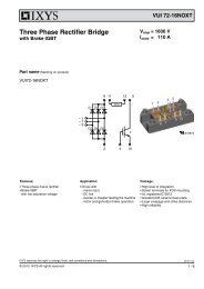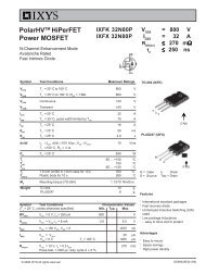
VUB 72-12/16NOXT - Europower Components Ltd
VUB 72-12/16NOXT - Europower Components Ltd
VUB 72-12/16NOXT - Europower Components Ltd

Create successful ePaper yourself
Turn your PDF publications into a flip-book with our unique Google optimized e-Paper software.
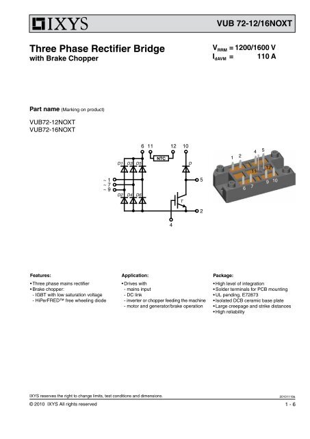
<strong>VUB</strong> <strong>72</strong>-<strong>12</strong>/<strong>16NOXT</strong>Chopper IGBT TRatingsSymbol Definitions Conditions min. typ. max. UnitV CEScollector emitter voltage T VJ = 25°C to 150°C <strong>12</strong>00 VV GESmax. DC gate voltage continuous -20 +20 VI C25collector current DC T C = 25°CI C80 DC T C = 80°CV CE(sat)collector emitter saturation voltage I C = 35 A; V GE = 15 V T VJ = 25°CT VJ = <strong>12</strong>5°C1.852.155840AA2.2 VV GE(th)gate emitter threshold voltage I C = 1 mA T VJ = 25°C 5.4 6.5 VI CEScollector emitter leakage current V CE = V CES ; V GE = 0 V T VJ = 25°CT VJ = <strong>12</strong>5°C 0.10.1 mAmAI GESgate emitter leakage current V CE = 0 V; V GE = ±20 V 500 nAt d(on)t rt d(off)t fE onE offturn-on delay timecurrent rise timeturn-off delay timecurrent fall timeturn-on energy per pulseturn-off energy per pulseinductive load T VJ = <strong>12</strong>5°CV CE = 600 V; I C = 35 AV GE = ±15 V; R G = 27 W; L = 100 µHQ Gon V CE = 600 V; V GE = 15 V; I C = 35 A 110 nCI CMreverse bias safe operating area RBSOA; V GE = ±15 V; R G = 27 W; L = 100 µHV CEK clamped inductive load; T VJ = <strong>12</strong>5°Ct SC(SCSOA)short circuit safe operating area V CE = 900 V; V GE = ±15 V; T VJ = <strong>12</strong>5°CR G = 27 W; non-repetitive70402501003.84.170< V CES -L S·d I /dtnsnsnsnsmJmJAV10 µsR thJCthermal resistance junction to case 0.65 K/WR thCHthermal resistance case to heatsink with heat transfer paste, see mounting instructions 0.9 K/WChopper Diode DRatingsSymbol Definitions Conditions min. typ. max. UnitV RRMmax. repetitive reverse voltage T VJ = 150°C <strong>12</strong>00 VI F25I F80forward current DC T C = 25°CT C = <strong>12</strong>5°CV Fforward voltage I F = 25 A T VJ = 25°CT VJ = <strong>12</strong>5°CI Rreverse current V R = V RRM T VJ = 25°CT VJ = <strong>12</strong>5°C 0.1I RMreverse recovery currentI F = 15 A; V R = 600 V T VJ = <strong>12</strong>5°C16t rrreverse recovery timedi F /dt = -400 A/µs130IXYS reserves the right to change limits, test conditions and dimensions.20101119a© 2010 IXYS All rights reserved 2 - 62.<strong>72</strong>.02515AA3.1 VV0.1 mAmAAnsR thJCthermal resistance junction to case 2.3 K/WR thJHthermal resistance case to heatsink with heat transfer paste 3.<strong>12</strong> K/WEquivalent Circuits for SimulationIRatingsSymbol Definitions Conditions min. typ. max. UnitV 0R 0V 0R 0Diode D1 - D6 T VJ = <strong>12</strong>5°C 0.857V 0 IGBT T T VJ = 150°C 1.1R 0 40V 0 Diode D T VJ = <strong>12</strong>5°C 1.25R 0 32VmWVmWVmW
<strong>VUB</strong> <strong>72</strong>-<strong>12</strong>/<strong>16NOXT</strong>Outline Drawing Dimensions in mm (1 mm = 0.0394“)4,6±115,8 ±10,5+0,25±1Ø0,5R20,2535632631,6501475,56789105,523,515<strong>12</strong>345131<strong>72</strong>±0,238,64x45°R1R±0,1±0,253,3 ±0,514 ±0,3±0,37 ±0,3±0,3R11 ±0,311 ±0,38,3±<strong>12</strong>5,75±0,150,551,5±0,3Product MarkingOrdering Part Name Marking on Product Delivering Mode Base Qty Ordering CodeStandard <strong>VUB</strong> <strong>72</strong>-<strong>12</strong>NOXT <strong>VUB</strong><strong>72</strong>-<strong>12</strong>NOXT Box 10 510734Standard <strong>VUB</strong> <strong>72</strong>-<strong>16NOXT</strong> <strong>VUB</strong><strong>72</strong>-<strong>16NOXT</strong> Box 10 510741IXYS reserves the right to change limits, test conditions and dimensions.20101119a© 2010 IXYS All rights reserved 4 - 6
<strong>VUB</strong> <strong>72</strong>-<strong>12</strong>/<strong>16NOXT</strong>80500I F[A]7060504030typ.T VJ= 25°CT VJ= 150°Cmax.I FSM[A]400300200V R= 0.8V RRMT VJ= 45°C201000.0 0.5 1.0 1.5 2.0V F[V]Fig. 1 Forward current vs. voltagedrop per rectifier diode100T VJ= 150°C00.001 0.01 0.1 1t [s]Fig. 2 Surge overload current perrectifier diode807010000V R= 0 VI dAVM605040[A]30201000I 2 t[A 2 s]100T VJ= 45°CT VJ= 150°C1000 40 80 <strong>12</strong>0 160T H[°C]Fig. 3 Max. forward current vs. heatsinktemperature (Rectifier bridge)101 10t [ms]Fig. 4 I 2 t versus time perrectifier diode140<strong>12</strong>0100P tot 80[W] 604020R thHA[K/W]0.511.5234600 10 20 30 40 50 60I dAVM[A]0 40 80 <strong>12</strong>0 160T A[°C]Fig. 5 Power dissipation vs. direct output current & ambient temperature (Rectifier bridge)IXYS reserves the right to change limits, test conditions and dimensions.20101119a© 2010 IXYS All rights reserved 5 - 6
<strong>VUB</strong> <strong>72</strong>-<strong>12</strong>/<strong>16NOXT</strong>I C[A]7060504030V GE= 15 VT VJ= 25°CT VJ= <strong>12</strong>5°CI C[A]7060504030T VJ= <strong>12</strong>5°CV GE= 15 V17 V19 V13 V11 V9 V2020101000.0 0.5 1.0 1.5 2.0 2.5 3.0 3.5V CE[V]Fig. 6 IGBT, typ. output characteristics00 1 2 3 4 5V CE[V]Fig. 7 IGBT, typ. output characteristicsE1086R G= 27 ΩV CE= 600 VV GE= ±15 VT VJ= <strong>12</strong>5°CE onE offE65I C= 35 AV CE= 600 VV GE= ±15 VT VJ= <strong>12</strong>5°CE on[mJ]4[mJ]4E off200 20 40 60 80I CE[A]Fig. 8IGBT, typ. switching energyversus collector current320 30 40 50 60 70 80R G[Ω]Fig. 9 IGBT, typ. switching energyversusgate resistance10 010 -1Z thJC[K/W]10 1 t [s]1000010 -2chopper dioderectifier diodeIGBTR[Ω]100010010 -3single pulse10 -410 -5 10 -4 10 -3 10 -2 10 -1 10 0 10 1Fig. 10 Typ. transient thermal impedance10-20 0 20 40 60 80 100 <strong>12</strong>0 140 160T [°C]Fig. 11 Typ. thermistor resistace vs. temperatureIXYS reserves the right to change limits, test conditions and dimensions.20101119a© 2010 IXYS All rights reserved 6 - 6
<strong>VUB</strong> <strong>72</strong>-<strong>12</strong>/<strong>16NOXT</strong>I F40353025T VJ= 25°C100°C150°CQ r3.02.52.0T VJ= <strong>12</strong>5°CV R= 800 VI F= 30 A[A]2015105[µC]1.51.00.5I F = 15 AI F = 7.5 A00 1 2 3 4V F[V]Fig. <strong>12</strong> Forward current I Fversus V F0.0100-di F/dt [A/µs]1000Fig. 13 Typ. reverse recovery chargeQ r versus -di F /dt5040T VJ= <strong>12</strong>5°CV R= 800 V2.01.5I RM[A]3020I F= 30 AI F = 15 AI F = 7.5 AK f1.0100.5I RMQ r00 200 400 600 800 1000-di F/dt [A/µs]Fig. 14 Typ. peak reverse currentI RMversus -di F/dt0.00 40 80 <strong>12</strong>0 160T VJ[°C]Fig. 15 Dynamic parametersQ r, I RMversus T VJ180160T VJ= <strong>12</strong>5°CV R= 800 VI F= 30 A<strong>12</strong>080T VJ= <strong>12</strong>5°CI F= 15 AV R= 800 V1.20.8t rr[ns]140I F = 15 AI F = 7.5 AV FR[V]t fr[µs]<strong>12</strong>0400.41000 200 400 600 800 1000-di F/dt [A/µs]Fig. 16 Typ. recovery timet rrversus -di F/dtV FR00.00 200 400 600 800 1000-di F/dt [A/µs]Fig. 17 Typ. peak forward voltageV FRand t frversus di F/dtt frIXYS reserves the right to change limits, test conditions and dimensions.20101119a© 2010 IXYS All rights reserved 7 - 6