DAC08 Data Sheet
DAC08 Data Sheet
DAC08 Data Sheet

You also want an ePaper? Increase the reach of your titles
YUMPU automatically turns print PDFs into web optimized ePapers that Google loves.
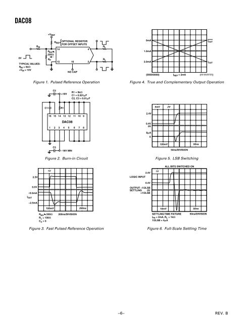
<strong>DAC08</strong>+V REF0VR INTYPICAL VALUES:R IN = 5k+V IN = 10VR EQ200R PR REF14OPTIONAL RESISTORFOR OFFSET INPUTS15 16NO CAP42R LR L0mAI OUT1.0mA2.0mA(0000|0000) I REF = 2mAI OUT(1111|1111)Figure 1. Pulsed Reference OperationFigure 4. True and Complementary Output OperationC2+18VR1 = 9kC1 = 0.001FC2, C3 = 0.01FC1R15mV2V16 15 14 13 12 11 10 9<strong>DAC08</strong>1 2 3 4 5 6 7 82.4V0.4V0V8A0C3–18V MIN100mV50ns/DIVISION50nsFigure 2. Burn-in CircuitFigure 5. LSB SwitchingALL BITS SWITCHED ON2.5V1V2.4VLOGIC INPUT1V0.4V0.5V–0.5mAOUTPUT –1/2LSBSETTLING 0V+1/2LSBI OUT–2.5mA100mV200ns10mV50nsR EQ 200R L = 100C C = 0200ns/DIVISIONSETTLING TIME FIXTUREI FS = 2mA, R L = 1k1/2LSB = 4A50ns/DIVISIONFigure 3. Fast Pulsed Reference OperationFigure 6. Full-Scale Settling Time–6–REV. B