Wire Wound Chip Inductor LCWC Series - AVX
Wire Wound Chip Inductor LCWC Series - AVX
Wire Wound Chip Inductor LCWC Series - AVX

Create successful ePaper yourself
Turn your PDF publications into a flip-book with our unique Google optimized e-Paper software.
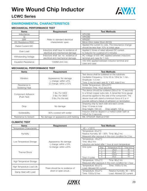
<strong>Wire</strong> <strong>Wound</strong> <strong>Chip</strong> <strong>Inductor</strong><strong>LCWC</strong> <strong>Series</strong>ENVIRONMENTAL CHARACTERISTICSMECHANICAL PERFORMANCE TESTItems Requirement Test MethodsInductanceHP4286QHP4286SRF Refer to standard electrical HP4287DC Resistance RDC characteristic spec. Micro-Ohm meter (Gom-801G)Rated Current IDCApplied the current to coils, The inductance changeshould be less than 10% to initial valueOver Load<strong>Inductor</strong>s shall have no evidence of Applied 2 times of rated allowed DC currentelectrical and mechanical damage to inductor for a period of 5 minutesWithstanding Voltage<strong>Inductor</strong>s shall be no evidence of AC voltage of 500 VAC applied between inductorselectrical and mechanical damage. terminal and case for 1 min.Insulation Resistance1000M ohm min.100 VDC applied between inductor terminal andcase and caseMECHANICAL PERFORMANCE TESTItems Requirement Test MethodsTest device shall be soldered on the substrateOscillation Frequency: 10 to 55 to 10Hz for 1 min.VibrationAppearance: No damageAmplitude: 1.5 mmL change: within ±5%Time: 2 hrs for each axis (X, Y &Z), total 6 hrsQ change: within ±10%Resistance toSolder Temperature: 260±50ºCSoldering HeatImmersion Time: 10±2 secondsThe device should be soldered (260±5 for 10 seconds)1 lbs. For 0402 to a tinned copper subs rate. A dynamiter force gaugeComponent Adhesion2 lbs. For 0603 should be applied to the side of the component. The(Push Test)3 lbs. For the rest device must with stand a minimum force of 2 or 4pounds without a failure of adhesion on terminationDropping chip by each side and each corner.Drop No damage Drop 10 times in totalDrop height: 100 cm Drop weight: 125 gSolderability90% covered with solder<strong>Inductor</strong> shall be dipped in a melted solder bath at245±5 for 3 secondsResistance to Solvent No damage on appearance and marking MIL-STD202F, Method 215DCLIMATIC TESTItems Requirement Test MethodsTemperature Characteristic-40 ~ +125°CTemperature: 40±2°CHumidityRelative Humidity: 90 ~ 95% Time: 96±2 hrsMeasured after exposure in the room condition for 2 hrsTemperature: -40±2°CLow Temperature Storage Appearance: No damage Time: 96±2 hrsL change: within ±10%<strong>Inductor</strong>s are tested after 1 hour at room temperatureQ change: within ±20%One cycle:Thermal ShockHigh Temperature StorageHigh Temperature Load LifeDamp Heat with LoadStep Temperature (°C) Time (min.)1 -25±3 302 25±2 153 125±3 304 25±2 15Total: 5 cyclesTemperature: 125±2°C Time: 96±2 hrsMeasured after exposure in the room condition for 1 hourTemperature: 85±2°C Time: 1000±12 hrsThere should be no evidence of Load: Allowed DC currentshort or open circuit. Temperature: 40±2°C Relative Humidity: 90 ~ 95%Time: 1000±12 hrs Load: Allowed DC current29