4048 - Komponenten
4048 - Komponenten
4048 - Komponenten

You also want an ePaper? Increase the reach of your titles
YUMPU automatically turns print PDFs into web optimized ePapers that Google loves.
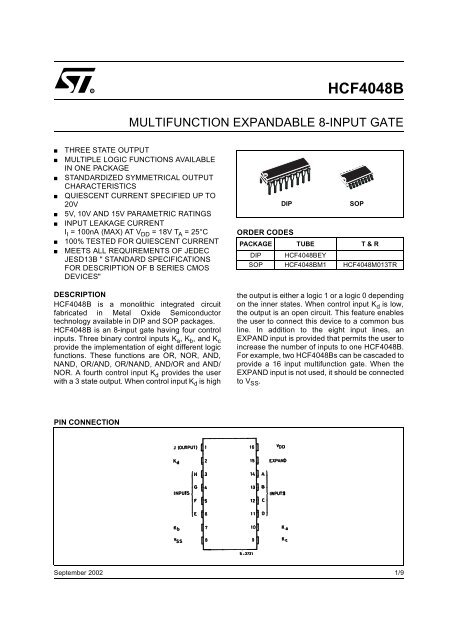
HCF<strong>4048</strong>BMULTIFUNCTION EXPANDABLE 8-INPUT GATE■■■■■■■■THREE STATE OUTPUTMULTIPLE LOGIC FUNCTIONS AVAILABLEIN ONE PACKAGESTANDARDIZED SYMMETRICAL OUTPUTCHARACTERISTICSQUIESCENT CURRENT SPECIFIED UP TO20V5V, 10V AND 15V PARAMETRIC RATINGSINPUT LEAKAGE CURRENTI I = 100nA (MAX) AT V DD = 18V T A = 25°C100% TESTED FOR QUIESCENT CURRENTMEETS ALL REQUIREMENTS OF JEDECJESD13B " STANDARD SPECIFICATIONSFOR DESCRIPTION OF B SERIES CMOSDEVICES"DIPSOPORDER CODESPACKAGE TUBE T & RDIP HCF<strong>4048</strong>BEYSOP HCF<strong>4048</strong>BM1 HCF<strong>4048</strong>M013TRDESCRIPTIONHCF<strong>4048</strong>B is a monolithic integrated circuitfabricated in Metal Oxide Semiconductortechnology available in DIP and SOP packages.HCF<strong>4048</strong>B is an 8-input gate having four controlinputs. Three binary control inputs K a , K b , and K cprovide the implementation of eight different logicfunctions. These functions are OR, NOR, AND,NAND, OR/AND, OR/NAND, AND/OR and AND/NOR. A fourth control input K d provides the userwith a 3 state output. When control input K d is highthe output is either a logic 1 or a logic 0 dependingon the inner states. When control input K d is low,the output is an open circuit. This feature enablesthe user to connect this device to a common busline. In addition to the eight input lines, anEXPAND input is provided that permits the user toincrease the number of inputs to one HCF<strong>4048</strong>B.For example, two HCF<strong>4048</strong>Bs can be cascaded toprovide a 16 input multifunction gate. When theEXPAND input is not used, it should be connectedto V SS .PIN CONNECTIONSeptember 20021/9
HCF<strong>4048</strong>BINPUT EQUIVALENT CIRCUITPIN DESCRIPTIONPIN No SYMBOL NAME AND FUNCTION14, 13, 12,11A, B, C, D Data Inputs6, 5, 4, 3 E, F, G, H Data Inputs10, 7, 9 K a , K b , K c Function Control Inputs2 K d 3-State Control Inputs1 J Data Output15 EXPAND Expand Input8 V SS Negative Supply Voltage16 V DD Positive Supply VoltageFUNCTIONAL DIAGRAMTRUTH TABLEOutput Function Boolean Expression K a K b K c Unused InputNOR J = A + B + C + D + E + F + G + H 0 0 0 V SSOR J = A + B + C + D + E + F + G + H 0 0 1 V SSOR/AND J = (A + B + C + D) • (E + F + G + H) 0 1 0 V SSOR/NAND J = (A + B + C + D) • (E + F + G + H) 0 1 1 V SSAND J = ABCDEFGH 1 0 0 V DDNAND J = ABCDEFGH 1 0 1 V DDAND/NOR J = ABCD + EFGH 1 1 0 V DDAND/OR J = ABCD + EFGH 1 1 1 V DDK d = 1 - NORMAL INVERTER ACTIONK d = 0 - HIGH IMPEDANCE OUTPUT2/9
HCF<strong>4048</strong>BLOGIC DIAGRAMABSOLUTE MAXIMUM RATINGSSymbol Parameter Value UnitV DD Supply Voltage -0.5 to +22 VV I DC Input Voltage -0.5 to V DD + 0.5 VI I DC Input Current ± 10 mAP D Power Dissipation per Package 200 mWPower Dissipation per Output Transistor 100 mWT op Operating Temperature -55 to +125 °CT stg Storage Temperature -65 to +150 °CAbsolute Maximum Ratings are those values beyond which damage to the device may occur. Functional operation under these conditions isnot implied.All voltage values are referred to V SS pin voltage.RECOMMENDED OPERATING CONDITIONSSymbol Parameter Value UnitV DD Supply Voltage 3 to 20 VV I Input Voltage 0 to V DD VT op Operating Temperature -55 to 125 °C3/9
HCF<strong>4048</strong>BDC SPECIFICATIONSTest ConditionValueSymbolParameterV I(V)V O(V)|I O |(µA)V DD(V)T A = 25°C -40 to 85°C -55 to 125°CMin. Typ. Max. Min. Max. Min. Max.UnitI L Quiescent Current 0/5 5 0.01 0.25 7.5 7.50/10 10 0.01 0.5 15 150/15 15 0.01 1 30 300/20 20 0.02 5 150 150V OH High Level Output 0/5
HCF<strong>4048</strong>BDYNAMIC ELECTRICAL CHARACTERISTICS (T amb = 25°C, C L = 50pF, R L = 200KΩ, t r = t f = 20 ns)SymbolParameterTest Condition Value (*) UnitV DD (V) Min. Typ. Max.t PHL t PLHt PHZ, t PLZt PZH, t PZLt TLH t THL Output Transition Time 5 100 20010 50 100 ns15 40 803-State Output Capacitance 5 10 pF(*) Typical temperature coefficient for all V DD value is 0.3 %/°C.TEST CIRCUITPropagation Delay TimeInputs to Output and K a toOutputPropagation Delay TimeK b to OutputPropagation Delay TimeK c to OutputPropagation Delay TimeEXPAND Input to Output3 - State PropagationDelay Time K d to Output5 300 60010 150 30015 120 2405 225 45010 85 17015 55 1105 140 28010 50 10015 40 805 190 38010 90 18015 65 130580 16010 RL = 1KΩ35 7015 25 50nsnsnsnsnsTESTSWITCHt PLH , t PHLt PZL , t PLZt PZH , t PHZC L = 50pF or equivalent (includes jig and probe capacitance)R L = 200KΩR T = Z OUT of pulse generator (typically 50Ω)OpenV DDV SS5/9
HCF<strong>4048</strong>BWAVEFORM 1 : PROPAGATION DELAY TIMES (f=1MHz; 50% duty cycle)WAVEFORM 2 : OUTPUT ENABLE AND DISABLE TIME (f=1MHz; 50% duty cycle)6/9
HCF<strong>4048</strong>BPlastic DIP-16 (0.25) MECHANICAL DATADIM.mm.inchMIN. TYP MAX. MIN. TYP. MAX.a1 0.51 0.020B 0.77 1.65 0.030 0.065b 0.5 0.020b1 0.25 0.010D 20 0.787E 8.5 0.335e 2.54 0.100e3 17.78 0.700F 7.1 0.280I 5.1 0.201L 3.3 0.130Z 1.27 0.050P001C7/9
HCF<strong>4048</strong>BSO-16 MECHANICAL DATADIM.mm.inchMIN. TYP MAX. MIN. TYP. MAX.A 1.75 0.068a1 0.1 0.2 0.003 0.007a2 1.65 0.064b 0.35 0.46 0.013 0.018b1 0.19 0.25 0.007 0.010C 0.5 0.019c145˚ (typ.)D 9.8 10 0.385 0.393E 5.8 6.2 0.228 0.244e 1.27 0.050e3 8.89 0.350F 3.8 4.0 0.149 0.157G 4.6 5.3 0.181 0.208L 0.5 1.27 0.019 0.050M 0.62 0.024S8˚(max.)PO13H8/9
HCF<strong>4048</strong>BInformation furnished is believed to be accurate and reliable. However, STMicroelectronics assumes no responsibility for theconsequences of use of such information nor for any infringement of patents or other rights of third parties which may result fromits use. No license is granted by implication or otherwise under any patent or patent rights of STMicroelectronics. Specificationsmentioned in this publication are subject to change without notice. This publication supersedes and replaces all informationpreviously supplied. STMicroelectronics products are not authorized for use as critical components in life support devices orsystems without express written approval of STMicroelectronics.© The ST logo is a registered trademark of STMicroelectronics© 2002 STMicroelectronics - Printed in Italy - All Rights ReservedSTMicroelectronics GROUP OF COMPANIESAustralia - Brazil - Canada - China - Finland - France - Germany - Hong Kong - India - Israel - Italy - Japan - Malaysia - Malta - MoroccoSingapore - Spain - Sweden - Switzerland - United Kingdom - United States.© http://www.st.com9/9