

Simple Class A Amplifier - .pdf
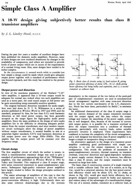
Simple Class A Amplifier - .pdf
Simple Class A Amplifier - .pdf

Create successful ePaper yourself
Turn your PDF publications into a flip-book with our unique Google optimized e-Paper software.
Wireless World, April 1969shown in Fig. l(c), would be more convenient in terms of sizeand cost, and would allow the load to be driven effectively inpush-pull if the inputs to the two transistors were of suitablemagnitude and opposite in phase. This requirement can beachieved if the driver transistor is connected as shown in Fig. 2.This method of connection also meets one of the mostimportant requirements of a low distortion amplifier-that thebasic linearity of the amplifier should be good, even in theabsence of feedback. Several factors contribute to this. There isthe tendency of the l c /Vb non-linearity of the characteristics ofthe output transistors to cancel, because during the part of thecycle in which one transistor is approaching cut-off the other isturned full on. There is a measure of internal feedback aroundthe loop Tr!, Tr2, Tr3 because of the effect which the baseimpedance characteristics of Tr! have on the output current ofTr3. Also, the driver transistor Tr3, which has to deliver a largevoltage swing, is operated under conditions which favour lowharmonic distortion-low output load impedance, high inputimpedance.A practical power amplifier circuit using this type of outputstage is shown in Fig. 3.The open loop gain of the circuit is approximately 600 withtypical transistors. The closed loop gain is determined, atfrequencies high enough for the impedance of C3 to be small incomparison to R4, by the ratio (R3 + R4) /R4. With the valuesindicated in Fig. 3, this is 13. This gives a feedback factor ofsome 34dB, and an output impedance of about 160 milliohms.Since the circuit has unity gain at d.c., because of theinclusion of C3 in the feedback loop, the output voltage, V e , isheld at the same potential as the base of Tr4 plus the baseemitter potential of Tr4 and the small potential drop along R3due to the emitter current of this transistor. Since the outputtransistor TrJ will turn on as much curren t as is necessary topull V e down to this value, the resistor R2, which together withR! controls the collector current of Tr2, can be used to set thestatic current of the amplifier output stages. It will also beapparent that V e can be set to any desired value by smalladjustments to Rs or R6• The optimum performance will beobtained when this is equal to half the supply voltage. (Half avolt or so either way will make only a small difference to themaximum output power obtainable, and to the other characteristicsof the amplifier, so there is no need for great precisionin setting this.)Silicon planar transistors are used throughout, and thisgives good thermal stability and a low noise level. Also, sincethere is no requirement for complementary symmetry, all thepower stages can use n-p-n transistors which offer, in silicon,the best performance and lowest cost. The overall performanceat an output level of 10 watts, or any lower level, more thanmeets the standards laid down by Williamson. The poweroutput and gain /frequency graphs are shown in Figs. 4-6, andthe relationship between output power and total harmonicdistortion is shown in Fig. 7. Since the amplifier is a straightforwardclass A circuit, the distortion decreases linearly withoutput voltage. (This would not necessarily be the case in aclass B system if any significant amount of cross-over distortionwas present.) The analysis of distortion components at levels ofthe order of 0.05% is difficult, but it appears that the residualdistortion below the level at which clipping begins is predominantlysecond harmonic.VINInputV1NO'5/iR 2R5100/i50VTr2C 2(22k stereo)3 9k1/4WVout+V149Tr 1RL Fig.2. Arrangementfor push-pull drive ofclass A stage.R 1R 21/2W1WTr2MJ4806100kC 11/4WTr 4R32N39062'7k(Motorola) 1/4WR5100k1/4W 8'2kAdjust 1/4Wso thatVE=1/2VC3250/i40VFig.3. Practical power amplifier circuit.14c 8 642VE'X'C 2lZ LTr 1MJ480(Motorola)+v09 1kOL-llL __________ L-________ __________ I10 50 100 1k 10k 100k 200kFrequency (Hz)FigA. Gain/frequency response curve of amplifier....:J10 2oI70kOL-llL __________ ________ ________ I10 50 100 1k 10k 100k 200kFrequency (Hz)Fig. 5. Output power/frequency response curve of amplifier.Stability, power output and load impedanceSilicon planar n-p-n transistors have, in general, excellent highfrequency characteristics, and these contribute to the very goodstability of the amplifier with reactive loads. The author has notyet found any combination of Land C which makes the systemunstable, although the system will readily become oscillatorywith an inductive load if R3 is shunted by a small condenser tocause roll-off at high frequencies.----Fig.6. Distortion/frequency curve at 9W.
150Wireless World, April 1969THD(%)0'30'2Onset ofclippingIIIITotal harmonic distortion Iat 1kHzIFig.7. Distortion/output power curve.0'10'05_ _ __ ._._._._._ . .. 2nd harmonico 1 2 3 4 5 6 7 8 9 10 11 12Output (watts)(22k for stereo)39k114WO,ospIn put ---I r-+--+680k114WTr5MPF103(Motorola)Sine wave performance at 1kHz. 9 watts, 15 ohm resistive load.Fundamental on scale of 10 V/cm. Distortion components on scaleof 50mV!cm with r.m.s. value of 0.05% .Fig.8. Modified inputcircuit for high inputimpedance.lOOpSOVlsMAdjustso thatVE=112VTr42N3906(Motorola)8'2k114WThe circuit shown in Fig. 3 may be used, with very littlemodification to the component values, to drive load impedancesin the range 3-15 ohms. However, the chosen output power isrepresented by a different current /voltage relationship in eachcase, and the current through the output transistors and theoutput-voltage swing will therefore also be different. Thepeak-voltage swing and the mean output current can becalculated quite simply from the well-known relationshipsW=PR and V=IR, where the symbols have their customarysignificance. (It should be remembered, however, that thecalculation of output power is based on r.m.s. values ofcurrent and voltage, that these must be multiplied by 1.414 toobtain the peak values, and that the voltage swing measured isthe peak-to-peak voltage, which is twice the peak value.)When these calculations have been made, the peak-to-peakvoltage swing for 10 watts power into a 15-ohm load is found tobe 34.8 volts. Since the two output transistors bottom at about0.6 volt each, the power supply must provide a minimum of 36volts in order to allow this output. For loads of 8 and 3 ohms,the minimum h.t. line voltage must be 27V and 17 voltsrespectively. The necessary minimum currents are 0.9, 1.2 and2.0 amps. Suggested component values for operation with theseload impedances are shown in Table 1. C3 and Cl togetherinfluence the voltage and power roll-off at low audio frequencies.These can be increased in value if a better low-frequencyperformance is desired than that shown in Figs. 4-6.Since the supply voltages and output currents involved leadto dissipations of the order of 17 watts in each outputtransistor, and since it is undesirable (for component longevity)to permit high operating temperatures, adequate heat sink areamust be provided for each transistor. A pair of separatelymounted 5in x 4in finned heat sinks is suggested. This is,unfortunately, the penalty which must be paid for class Aoperation. For supplies above 30V Trl and Tr2 should beMJ481s and Tr3 a 2N1613.Square wave response at 50Hz.r· r·1 ,-,1I ,IUWW l.i,iSquare wave response. Scale 10V!cm. Frequency 50kHz. 15 ohmresistive load.If the output impedance of the pre-amplifier is more than afew thousand ohms, the input stage of the amplifier should bemodified to include a simple f.e.t. source follower circuit, asshown in Fig. 8. This increases the harmonic distortion toabout 0.12%, and is therefore (theoretically) a less attractivesolution than a better pre-amplifier.A high frequency roll-off can then be obtained, if necessary,by connecting a small capacitor between the gate of the f.e.t.and the negative (earthy) line.Table 1. Summary of component combinations for differentload impedances.Zlv R, R 2C,c2V1N (r.m.s.)3fl 17V 2A 47fl 1 BOfl 500" 25V 5000" 25V 0.41VBfl 27V 1.2A 100fl 560fl 25011 40V 2500" 50V 0.66V15fl 36V 0.9 150fl 1.2kfl 250" 40V 2500" 50V 0.9VSuitable transistorsSome experiments were made to determine the extent to whichthe circuit performance was influenced by the type and currentgain of the transistors used. As expected the best performancewas obtained when high-gain transistors were used, and whenthe output stage used a matched pair. No adequate substitute
Wireless World, April 1969151is known for the 2N697/2N1613 type used in the driver stage,but examplesof this transistor type from three differentmanufacturers were used with apparently identical results.Similarly, the use ofalternative types of input trasistorproduced no apparent performance change, and the TexasInstruments 2N4058 is fully interchangeable with the Motorola2N3906 used in the prototype.The most noteworthy performance changes were found inthe current gain characteristics of the output transistor pair,and for the lowest possible distortion with any pair, the voltageat the point from which the loudspeaker is fed should beadjusted so that it is within 0.25 volt of half the supply linepotential. The other results are summarized in Table 2.The transistors used in these experiments were MotorolaMJ480/481, with the exception of (6), in which Texas 2S034devices were tried. The main conclusion which can be drawnfrom this is that the type of transistor used may not be veryimportant, but that if there are differences in the current gainsof the output transistors, it is necessary that the device withthe higher gain shall be used in the position of Trl•When distortion components were found prior to the onsetof waveform clipping, these were almost wholly due to thepresence of second harmonics.Output+---------(C31,000iJ40V2'2k0'252'7k0'25C,5,000iJ50V2·2k( b)(a)Constructional notes<strong>Amplifier</strong>. The components necessary for a 10 + 10 watt stereoamplifier pair can conveniently be assembled on a standard"Lektrokit" 4in x 4tin s.r.b.p. pin board, as shown in thephotographs, with the four power transistorsmounted onexternal heat sinks. Except where noted the values of componentsdo not appear to be particularly critical, and 10%tolerance resistors can certainly be used without ill effect. Thelowest noise levels will however be obtained with good qualitycomponents, and with carbon-film, or metal-oxide, resistors.Power supply. A suggested form of power supply unit isshown in Fig. 9 (a). Since the current demand of the amplieris substantially constant, a series transistor smoothing circuitcan be used in which the power supply output voltage may beadjusted by choice of the base current input provided by theTable 2. Relation of distortion to gain-matching in theoutput stage.Cu.rem gainDistortion(T.,) (T.,) (at 9 watts)1. 135 135 0.06%2. 40 120 0.4%3.120 40 0.12% (pair 2 reversed in position)4. 120 lOO 0.09%Fig. 9. (a) Power supply unit, and (b) parallel connected transistorsfor high currents.emitter follower Tr2 and the potentiometer VR1• With thevalues of reservoir capacitor shown in Table 3, the ripple levelwill be less than lOm V at the rated output current, providedthat the current gain of the series transistors is greater than 40.For output currents up to 2.5 amps, the series transistorsindicated will be adequate, provided that they are mounted onheat sinks appropriate to their loading.However, at the current levels necessary for operation of the3-ohm version of the amplifier as a stereo pair, a single MJ480will no longer be adequate, and either a more suitable seriestransistor must be used, such as the Mullard BDY20, with forexample a 2N1711 as Tr2, or with a parallel connected arrangementas shown in Fig. 9(b).The total resistance in the rectifier "primary" circuit, includingthe transformer secondary winding, must not be lessthan0.25 Q. When the power supply, with or without anamplifier, is to be used with an r.f. amplifier-tuner unit, it maybe necessary to add a 0.251JF (160V.w.) capacitor across thesecondary winding of T I to prevent transient radiation. Therectifier diodes specified are International Rectifier pottedbridgetypes.5. 100 120 0.18% (pair 5 reversed)6.50 40 0.1%Transistor protection circuitTable 3. Power-supply components.AMPZL lOUT VOUTC, T',/2 MR115Q lA 37V 1000" MJ480 5805 40V50V2N6972x 15Q 2A 37V 5000" MJ480 5805 40V50V2N6978Q 1.25A 27V 2000" MJ480 5805 30V40V2N6972x 8Q 2.5A 27V 50001' MJ480 5805 30V40V2N6973Q 1.9A 18V 50001' MJ480 5B05 20V30V2N6972x 3Q 3.8A 18V 10.000" MJ480 7B05T 20V30V2x2N697T,lA2A1.25A2.5A2A4AThe current which flows in the output transistor chain (Trl>Tr2) is determined by the potential across Tr2, the values of RIand R2, and the current gain and collector-base leakage currentof Tr2• Since both of these transistor characteristics are temperaturedependent the output series current will increasesomewhat with the temperature of Tr2• If the amplifier is to beoperated under conditions of high ambient temperature, or iffor some reason it is not practicable to provide an adequate areaof heat-sink for the output transistors, it will be desirable toprovide some alternative means for the control of the outputtransistor circuit current. This can be done by means of thecircuit shown in Fig. 10. In this, some proportion of the d.c.bias current to Tr. is shunted to the negative line throughTr 7' when the total current flowing causes the potentialapplied to the base of Tr6 to exceed the turn-on value (about
152Wireless World, April 1969v_---_--.J'VVV'-- .. ---+Power Suppiy1.0.Tr72N3904(Motorola)To base of T r,_--1'c..100 Set current-.!V\i\I'- .. ---.to requiredvalue4701/2W Tr6BC212L(Texas)+------...lk1/2W4-7k1/2WFig.10. <strong>Amplifier</strong> current regulation circuit.0.5 volt). This allows very precise control of the series currentwithout affecting the output power or distortion characteristics.The simpler arrangement whereby the current controlpotential for Tr7 is obtained from a series resistor in the emittercircuit of Trj leads, unfortunately, to a worsening of thedistortion characteristics to about 0.15% at 8 watts, rising toabout 0.3% at the onset of overload.Layout of single channel of 10+ 10 watt amplifier on standard4in X 4fin 'Lektrokit' s. r.b.p. pin board.Performance under listening conditionsIt would be convenient if the performance of an audioamplifier (or loudspeaker or any other similar piece of audioequipment) could be completely specified by frequency responseand harmonic distortion characteristics. Unfortunately,it is not possible to simulate under laboratory conditions thecomplex loads or intricate waveform structures presented tothe amplifier when a loudspeaker system is employed toreproduce the everyday sounds of speech and music; so thatalthough the square wave and low-distortion sine wave oscillators,the oscilloscope, and the harmonic distortion analyser arevaluable tools in the design of audio circuits, the ultimate testof the final design must be the critical judgment of the listenerunder the most carefully chosen conditions his facilities andenvironment allow.The possession of a good standard of reference is a great helpin comparative trials of this nature, and the author has beenfortunate in the possession, for many years, of a carefully andexpensively built "Williamson" amplifier, the performance ofwhich has proved, in listening trials, to equal or exceed, bygreater or lesser margins, that of any other audio amplifier withwhich the author has been able to make comparisons.However, in the past, when these tests were made forpersonal curiosity, and some few minutes could elapse in thetransfer of input and output leads from one amplifier to theother, the comparative performance of some designs has been soclose that the conclusion drawn was that there was really verylittle to choose between them. Some of the recent transistorpower amplifier circuits gave a performance which seemedfully equal to that of the "Williamson", at least so far as onecould remember during the interval between one trial and thenext. It was, however, appreciated that this did not really offerthe best conditions for a proper appraisal of the more subtledifferences in the performance of already good designs, so achangeover switch was arranged to transfer inputs and outputsbetween any chosen pair of amplifiers, and a total of sixamplifier units was assembled, including the "Williamson", andanother popular valve unit, three class B transistor designs,including one of commercial origin, and the class A circuitdescribed above. The frequency response, and total harmonicdistortion characteristics, of the four transistor amplifiers wastested in the laboratory prior to this trial, and all were found toUnderside of completed amplifier, with base cover removed, showingexternal box-form heat sink.Looking down on the completed amplifier.
Wireless World, April 1969have a flat frequency response through the usable audiospectrum, coupled with low harmonic distortion content (theworst-case figure was 0.15%).In view of these prior tests, it was not expected that therewould be any significant difference in the audible performanceof any of the transistor designs, or between them and the valveamplifiers. It was therefore surprising to discover, in the event,that there were discernible differences between the valve andthe three class B transistor units. In fact, the two valve designsand the class A transistor circuit, and the three class B designsformed two tonally distinct groups, with closely similar characteristicswithin each group. The "Williamson" and the presentclass A design were both better than the other valve amplifier,and so close in performance that it was almost impossible to tellwhich of the two was in use without looking at the switchposition. In the upper reaches of the treble spectrum thetransistor amplifier has perhaps a slight advantage.The performance differences between the class A and theclass B groups were, however, much more prominent. Not onlydid the class A systems have a complete freedom from the slight"edginess" found on some high string notes with all the class Bunits, but they appeared also to give a fuller, "rounder",quality, the attractiveness of which to the author muchoutweighs the incidental inconvenience of the need for moresubstantial power supply equipment and more massiveheat sinks.Some thought, in discussions with interested friends, hasbeen given to the implications of this unlooked-for discovery,and a tentative theory has been evolved which is offered for whatit is worth. It is postulated that these tonal differences arisebecause the normal moving-coil loudspeaker, in its associatedhousing, can present a very complex reactive load at frequenciesassociated with structural resonances, and that this mightprovoke transient overshoot when used with a class B amplifier,when a point of inflection in the applied waveform chanced tocoincide with the point of transistor crossover, at which point,because of the abrupt change in the input parameters of theoutput transistors the loop stability margins and outputdamping will be less good. In these circumstances, the desiredfunction of the power-amplifier output circuit in damping outthe cone-response irregularities of the speaker may be performedworse at the very places in the loudspeaker frequencyresponsecurve where the damping is most needed.It should be emphasized that the differences observed inthese experiments are small, and unlikely to be noticed exceptin direct side-by-side comparison. The perfectionist may,however, prefer class A to class B in transistor circuitry if hecan get adequate output power for his needs that way.Listener fatigueIn the experience of the author, the performance of mostwell-designed audio power amplifiers is really very good, andthe differences between one design and another are likely to besmall in comparison with the differences between alternativeloudspeaker systems, for example, and of the transistor designsso far encountered, not one could be considered as unpleasingto the ear. However, with the growing use of solid-state poweramplifiers, puzzling tales of "listener fatigue" have been heardamong the cognoscemi, as something which all but the mostexpensive transistor amplifiers will cause the listener, in contradistinctionwith good valve-operated amplifiers. This seemedto be worth investigation, to discover whether there was anyfoundation for this allegation.In practice it was found that an amplifier with an impeccableperformance on paper could be quite worrying to listen tounder certain conditions. This appears to arise and be particularlyassociated with transistor power amplifiers because mostof these are easily able to deliver large amounts of power atsupersonic frequencies, which the speakers in a high qualitysystem will endeavour to present to the listener. In this contextit should be remembered that in an amplifier which has a flatpower response from 30Hz to 180kHz, 90% of this powerspectrum will be supersonic.This unwanted output can arise in two ways. It can bebecause of wide spectrum "white noise" from a preamplifierwith a significant amount of hiss-this can happen if a valvepreamplifier is mismatched into the few thousand ohms inputimpedance of a transistor power amplifier, and will also causethe system performance to be unnaturally lacking in bass.Trouble of this type can also arise if transient instability orhigh frequency "ringing" occurs, for example when a reactiveload is used with a class B amplifier having poor cross-overpoint stability.REFERENCE1. Bailey, A.R., "High-performance Transistor <strong>Amplifier</strong>", WirelessWorld, November 1966; "3Q-Watt High Fidelity <strong>Amplifier</strong>", May 1968;and "Output Transistor Protection in A.F. <strong>Amplifier</strong>s", June 1968.Conferences and ExhibitionsLONDONApr. 21-25Switching Techniques for Telecommunication Networks(LE.E., Savoy PI., London W.C.2)Apr. 22-30153Savoy PlaceOlympiaEngineering and Marine Exhibition(F. W. Bridges & Sons, Commonwealth House, New Oxford St., London W.C.!)EXETERApr. 1 & 2The UniversityApplications of R.F. Spectroscopy to the Electronic Structure of Solids(Dr. J. E. Cousins, The University, Exeter)KlNGSTON-ON-THAMESApr. 1 & 2Digital Storage TchniquesCol. of Technology(Dr. R. V. Sharman, College of Technology, Penrhyn Rd., Kingston-on-Thames)SOUTHAMPTONApr. 15-18YORKComputer Aided Design(LE.E., Savoy PI., London W.C.2)Apr. 16-18Thin Films Conference(LP.P.S., 47 Belgrave Sq., London S.W.1)OVERSEASApr. 8-10Computer Processing in Communications(Polytechnic Inst. of Brooklyn, 333 Jay St., Brooklyn, N.Y. 10021)Apr. 11-14Semiconductor Device ResearchThe UniversityThe University(Dr. H. H. Burghoff, VDE Haus, Stresemann Allee 21, 6 Frankfurt am Main)Apr. 15-18Magnetics ConferenceNew YorkMunichAmsterdam(Dr. Th. Holtwijk, Philips Research Laboratories, Eindhoven, Netherlands)Apr. 16-18WashingtonGeoscience Electronics(LE.E.E., 345 E.47th St., New York, N.Y. 10017)Apr. 19 & 20Amateur Television Congress(Club Francais de Television d'Amateur, 13 rue de Bellevue, Paris 19)Apr. 21 & 22Circuit Theory Symposium(University of Texas, Austin, Texas)Apr. 22-24Telemetering Conference(LE.E.E., 345 E.47th St., New York, N.Y. 10017)Apr. 23-25ArmentieresAustinWashingtonLexingtonElectronic Crime Countermeasures0. S. Jackson, College of Engineering, University of Kentucky, Lexington)Apr. 30-May 2WashingtonElectronic Components Conference(LE.E.E., 345 E.47th St., New York, N.Y. 10017)