Electrical Biomolecule Detection Using Nanopatterned ... - KAIST
Electrical Biomolecule Detection Using Nanopatterned ... - KAIST
Electrical Biomolecule Detection Using Nanopatterned ... - KAIST

Create successful ePaper yourself
Turn your PDF publications into a flip-book with our unique Google optimized e-Paper software.
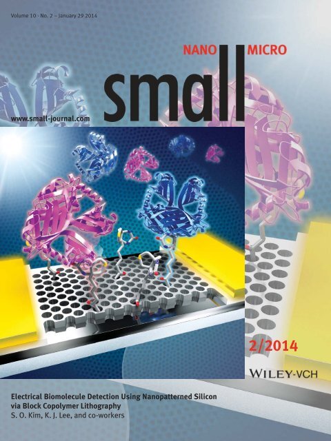
SMALL_10_2_cover.indd 11/15/14 9:31 AMVolume 10 · No. 2 – January 29 2014www.small-journal.com2 / 2014<strong>Electrical</strong> <strong>Biomolecule</strong> <strong>Detection</strong> <strong>Using</strong> <strong>Nanopatterned</strong> Siliconvia Block Copolymer LithographyS. O. Kim, K. J. Lee, and co-workers
Biosensors<strong>Electrical</strong> <strong>Biomolecule</strong> <strong>Detection</strong> <strong>Using</strong> <strong>Nanopatterned</strong>Silicon via Block Copolymer LithographyChang Kyu Jeong , Hyeong Min Jin , Jae-Hyuk Ahn , Tae Jung Park , Hyeon Gyun Yoo ,Min Koo , Yang-Kyu Choi , Sang Ouk Kim ,* and Keon Jae Lee *A n electrical biosensor exploiting a nanostructured semiconductor is a promisingtechnology for the highly sensitive, label-free detection of biomolecules viaa straightforward electronic signal. The facile and scalable production of ananopatterned electrical silicon biosensor by block copolymer (BCP) nanolithographyis reported. A cost-effective and large-area nanofabrication, basedon BCP self-assembly and single-step dry etching, is developed for the hexagonalnanohole patterning of thin silicon films. The resultant nanopatterned electricalchannel modified with biotin molecules successfully detects the two proteins,streptavidin and avidin, down to nanoscale molarities (≈1 n M ). The nanoscale patterncomparable to the Debye screening length and the large surface area of the threedimensionalsilicon nanochannel enable excellent sensitivity and stability. A devicesimulation confirms that the nanopatterned structure used in this work is effective forbiomolecule detection. This approach relying on the scalable self-assembly principleoffers a high-throughput manufacturing process for clinical lab-on-a-chip diagnosesand relevant biomolecular studies.1 . IntroductionThe detection of biological elements, such as biomarkers, [ 1 ]viruses, [ 2 ] and pathogens, [ 3 ] is crucial for the early diagnosisand treatment of human diseases. Although enzyme-linkedimmunosorbent assay (ELISA) has been extensively usedfor biosensing, it is well known that ELISA has criticallimitations, such as complicated labeling steps, high analyteconcentration requirements, [ 4 ] and incompatibility withelectronic detection caused by difficulties of signal conversion.Various types of biosensors, including thermometric, [ 5 ]magnetic, [ 6 ] piezoelectric,[ 7 ] optical,[ 8,9 ] and electrical [ 10–14 ]biosensors, have been developed to surpass such limitations.Among them, the electrical biosensor using semiconductorC. K. Jeong, H. G. Yoo, Dr. M. Koo, Prof. K. J. LeeDepartment of Materials Science and EngineeringKorea Advanced Institute of Science and Technology (<strong>KAIST</strong>)291 Daehak-ro , Yuseong-gu , Daejeon 305–701 , Republic of KoreaE-mail: keonlee@kaist.ac.krH. M. Jin, Prof. S. O. KimCenter for Nanomaterials and Chemical ReactionsInstitute for Basic Science (IBS)Department of Materials Science and EngineeringKorea Advanced Institute of Science and Technology (<strong>KAIST</strong>)291 Daehak-ro , Yuseong-gu , Daejeon 305–701 , Republic of KoreaE-mail: sangouk.kim@kaist.ac.krDOI: 10.1002/smll.201301202J.-H. Ahn, Prof. Y.-K. ChoiDepartment of <strong>Electrical</strong> EngineeringKorea Advanced Institute of Scienceand Technology (<strong>KAIST</strong>)291 Daehak-ro , Yuseong-gu , Daejeon 305–701 ,Republic of KoreaDr. T. J. Park [+]BioProcess Engineering Research CenterCenter for Systems and Synthetic BiotechnologyInstitute for the BioCenturyKorea Advanced Institute of Science and Technology (<strong>KAIST</strong>)291 Daehak-ro , Yuseong-gu , Daejeon 305–701 , Republic of Korea[+] Present address: Department of Chemistry, Chung-Ang University, 84Heukseok-ro, Dongjak-gu, Seoul 156-756, Republic of Koreasmall 2014, 10, No. 2, 337–343© 2013 Wiley-VCH Verlag GmbH & Co. KGaA, Weinheim wileyonlinelibrary.com337
full papersC. K. Jeong et al.nanomaterials has been regarded as a strong candidate fornext-generation biosensors due to its high sensitivity, rapiddiagnosis without labeling steps, and compatibility with integratedcircuits. [ 15–17 ]The nanostructured channel in a field-effect transistor(FET) has been considered for potential use in high-performanceelectrical biosensors. The high sensitivity is facilitatedby the nano-dimensional channel, which is comparable tothe Debye screening length [ 18 ] and size of biomolecules. [ 15,19 ]To date, many research groups have reported bottom-upmethods for fabrication of carbon materials (e.g., carbonnanotubes and graphene) [ 20,21 ] or silicon nanowires [ 2,12,22 ] forthe high sensitivity of biosensors. However, these bottomupapproaches revealed drawbacks including the inaccuratepositioning of nanomaterials, the poor uniformity of dopinglevels, and the low integration density for ultimate commercialization.[ 13 ] In contrast, top-down approaches, such aselectron-beam lithography, have been successfully employedfor ultrafine nanoscale biosensors, including those reportedin our previous studies. [ 11,14 ] Nonetheless, the major limitationof top-down electron-beam nanofabrication lies in thehigh cost and extremely low throughput, which are inherentlyincompatible with large-scale manufacturing. [ 15 ]Block copolymer (BCP) self-assembly, which is generallydriven by the microphase separation of covalentlylinked incompatible polymer blocks, is able to form denseand ordered pattern arrays of even sub-10 nm features. [ 23,24 ]BCP self-assembly is considered to be a powerful and viabletool for nanolithography due to its excellent scalability, highpattern precision, and compatibility with the conventionalcomplementary metal oxide semiconductor process. [ 25,26 ]Many research groups have exploited BCP self-assembly fora variety of materials and applications. [ 27–31 ] For example,we have introduced BCP lithography for the nanoscale patterningof arbitrary substrate materials [ 32,33 ] up to wafer scalewith a few tens of nanometers-scale feature sizes.Herein, we report the electrical detection of biomoleculesusing an ultrathin Si nanomesh patterned by BCPlithography. Polystyrene- block -poly(methyl methacrylate)(PS- b -PMMA) thin films with vertically hexagonal cylindermorphology are employed as templates for single-step SF 6dry etching to generate a large-area Si nanomesh structure ofsub-20 nm-scale features. The nanomesh channel enables thebiosensor to monitor pH changes and detects two proteins ofsimilar structures: streptavidin and avidin. The performanceof the nanopatterned biosensor is compared with that of thenon-patterned counterpart to demonstrate the advantage ofthe nanopatterned structure for detection sensitivity. Technologycomputer-aided design (TCAD) device simulation isperformed to theoretically support the merits of the nanostructuredsemiconductor over non-patterned devices forbiomolecule detection.2 . Results and DiscussionThe overall fabrication scheme for the nanopatterned electricalbiosensor is illustrated in Figure 1 . The high-levelboron doping of the source and drain (S/D) regions isFigure 1. Schematic process for a nanopatterned electrical biosensor,including i) boron doping, ii) BCP spin-casting and self-assembly,iii) PMMA domain removal, and iv) pattern transfer to the top Si layer.v) An FET-based biosensor is functionalized with biotin molecules fordetecting streptavidin or avidin protein (BOX = buried oxide).performed on an ultrathin Si layer (≈25 nm) of a siliconon-insulator(SOI) wafer by ion implantation. After coveringS/D regions with a photoresist (PR; Figure 1 -i), thetop Si surface is covalently modified with poly(styrenerandom-methyl methacrylate) (P(S- r -MMA)) copolymer. APS- b -PMMA thin film is spin-cast and thermally annealed(250 °C) to induce microphase separation (Figure 1 -ii). TheBCP thin film spontaneously assembles into the morphologyof vertically hexagonal cylinders on the neutrally modifiedsurface due to an identical interfacial tension to PS andPMMA. The PMMA cylindrical nanodomains are selectivelyremoved by the sequential treatments of acetic acid solutionand O 2 plasma (Figure 1 -iii). The remaining PS templateafter PMMA etching is employed as a nanopatterned maskfor the following dry etching of the underlying Si layer. Asingle-step inductively coupled plasma reactive ion etching(ICP-RIE) using SF 6 gas is applied to the pattern transfer ofPS template morphology into the top Si layer (Figure 1 -iv).Notably, such a well-defined hexagonal nanohole PS templateendures the harsh dry etching during the completeetching of the Si layer, [ 34 ] which is differentiated from previousBCP studies that employed complicated multistep processes,including metal mask deposition. After the completeremoval of the remaining PS nanotemplate and PR patterns,the formation of the channel region and metal contacts iscarried out by using conventional photolithography and wet338 www.small-journal.com © 2013 Wiley-VCH Verlag GmbH & Co. KGaA, Weinheimsmall 2014, 10, No. 2, 337–343
<strong>Biomolecule</strong> <strong>Detection</strong> <strong>Using</strong> <strong>Nanopatterned</strong> SiliconFigure 3. The nanomesh PS template before Si etching for patterntransfer. a) Plane view (i) and 60° tilted view (ii) of SEM image ofremaining PS template after acetic acid wet treatment for PMMAelimination (average diameter of nanoholes: 40 nm, average widthbetween neighboring holes: 40 nm, thickness of PS template: 110 nm).b) Plane view (i) and 60° tilted view (ii) of SEM image of remaining PStemplate after subsequent O 2 plasma treatment for removing residualPMMA and widening the PS nanotemplate holes (average diameter ofnanoholes: 65 nm, average width between neighboring holes: 15 nm,thickness of PS template: 90 nm).Figure 2. a) SEM image of a nanopatterned Si channel. Moiréfringes over the entire channel region demonstrate the uniformityof the nanopatterned Si structure. b) Magnified SEM image of thenanopatterned Si channel. c) Cross-sectional SEM image of thehexagonal nanohole morphology of the top Si layer (≈25 nm thickness).etching. For the last stage, the nanochannel area is sequentiallyfunctionalized with a (3-aminopropyl)triethoxysilane(APTES) self-assembled monolayer (SAM) and biotin3-sulfo- N -hydroxysuccinimide ester (sulfo-NHS-biotin) forspecific binding with the streptavidin or avidin. [ 35 ] Figure 1 -vschematically presents the biosensor with a nanopatternedSi channel functionalized by biotin molecules. The biotin–streptavidin/avidin system used in our experiments hasserved extensively as a standard model for protein–ligandinteractions. [ 21 ]The nanopatterned Si channel fabricated by BCP lithographyis observed with scanning electron microscopy (SEM).Moiré fringes caused by the interference between instrumentalaliasing and sample grating are shown in Figure 2 a,[ 36 ]which confirms the uniformity of nanopattern transfer overthe entire channel region. In this work, a BCP template witha PS mesh-hole diameter of ≈40 nm is employed ( Figure 3 a-iand 3 a-ii).[ 37,38 ] The average hole diameter of PS patternsincreases up to ≈65 nm by O 2 over-etching (Figure 3 b-iand 3 b-ii), which realizes a Si nanomesh of ≈15 nm after thepattern transfer (Figure 2 b). This additional etching of PStemplate for the narrow Si nanopattern is important to fabricatethe nanoscale biosensor. Figure 2 c is a cross-sectionalSEM image of a nanopatterned channel, which indicates thatthe dry etching successfully transfers the nanopattern of PSmesh onto the entire top Si layer. [ 25,39 ] The nanomesh designof the Si channel is comparable to the screening length ofanalyte charges and thus ensures high sensing resolution forbiomolecule detection.Figure 4 a depicts the chemical modification steps of thenanopatterned Si channel for biosensing. The surface terminalgroup of an APTES-treated Si channel is composedof primary amines (–NH 2 ), protonated amines (–NH 3 + ),and hydroxyl groups (–OH), as confirmed by X-ray photoelectronspectroscopy (XPS) (Figure 4 b). For streptavidin oravidin detection, sulfo-NHS-biotin is linked with the aminegroup of APTES on the Si channel. There are four biotinbindingpockets in the proteins, but one or two of them canbe bound to the immobilized biotin. [ 35 ] The variation of thecurrent recording through the nanopatterned channel uponsurface functionalization is plotted in Figure 4 c. The currentdecreases upon silanization due to the positive charge of–NH 3 + groups of APTES. During the biotinylation step, thesulfo-NHS-biotin is immobilized through reaction with theprotonated amine as well as the primary amine of APTES-SAM. [ 35 ] As a result, the density of protonated aminegroups is considerably reduced on the nanopatterned Si,which consequently increases the current flow.The influence of the nanopattern on charge detectionsensitivity was evaluated by the conductance change of theAPTES-modified Si nanochannel with pH ( Figure 5 a). The–NH 3 + groups induced by the protonation of –NH 2 at lowpH [ 12 ] are able to deplete holes in a p-type nanopatternedSi channel and thereby reduce the conductance. By contrast,small 2014, 10, No. 2, 337–343© 2013 Wiley-VCH Verlag GmbH & Co. KGaA, Weinheimwww.small-journal.com339
full papersC. K. Jeong et al.Figure 4. a) Schematic diagram of the chemical functionalizationmethod for streptavidin or avidin protein binding onto the biotinylated Sichannel. i) Formation of APTES-SAM through silanization. ii) Biotinylationusing sulfo-NHS-biotin linked with immobilized APTES-SAM. iii) Biotinbindingprotein, streptavidin (negatively charged) or avidin (positivelycharged), attaches to the biotinylated Si channel. b) N1s XPS spectraof APTES immobilized on the Si channel: C–NH 2 peak (399.9 eV) andC–NH 3 + peak (401.9 eV). c) The current changes of the nanopatternedbiosensor are plotted during sequential surface functionalization steps.The current decreases after APTES silanization due to the formation of–NH 3 + charges. On the contrary, the fraction of –NH 3 + chemical groupsis considerably reduced by the subsequent biotinylation step, whichinduces the increase of current flow.at a high pH, –NH 3 + and –OH groups are deprotonated to–NH 2 and –O − , respectively (Figure S2, Supporting Information).The deprotonation negatively modifies the Si surface,which causes the increase of conductance (Figure 5 a). [ 12 ]Meanwhile, there is no noticeable current change with pHon the non-patterned device, as the short screening length ofsurface functional groups hardly influences the entire bulkchannel. A pH sensitivity of about 22.7 nS per pH unit isobtained in the nanopatterned channel, which is comparableto previous reports. [ 2 ] The small-scale range-bars of conductancechange in the nanopatterned channel indicate the goodreproducibility and reliability of our nanochannel-basedcharge detection.Figure 5 b and 5 c depict the detection of streptavidin andavidin, which have almost identical protein structures andsimilar affinity for biotin. [ 10 ] However, their opposite chargesat neutral pH caused by their different isoelectric points(pI)—streptavidin pI ≈5.6 and avidin pI ≈10.5—enable theirdistinguishable detection. [ 40 ] Figure 5 b shows that the currentlevel of the nanomesh biosensor increases while streptavidinproteins with negative charges are bound to the biotinylatedchannel in a phosphate-buffered saline (PBS, pH 7.4) solutionfor 5 min. This current increment is attributed to the holeaccumulation by negative charges and the potential barrierlowering in the nanomesh p-type channel, as illustrated by theinset of Figure 5 b. By contrast, the current level of the nanopatternedbiosensor decreases when avidin proteins are boundFigure 5. a) Conductance changes of nanopatterned (square symbols)and non-patterned channels (circle symbols) versus pH. The range-barsof conductance changes in the nanopatterned channel demonstratethe reliability of nanochannel-based charge detection. b) Normalizedcurrent changes upon streptavidin binding at the nanopatternedchannel. The inset illustrates the variation of valence band state ofthe channel upon streptavidin binding. c) Normalized current changesupon avidin binding at the nanopatterned channel. The inset illustratesthe variation of valence band state after avidin binding. d) Normalizedcurrent changes of the nonpatterned channel upon protein binding.No noticeable current change was observed. The normalized currentsare calculated from ( I − I 0 )/ I 0 and treated as absolute values ( I 0 : initialcurrent level before protein binding; I : changed current after proteinbinding).to the channel. The positively charged proteins induce thehole depletion and the potential barrier rise, as indicated inthe inset of Figure 5 c. Streptavidin and avidin concentrationsdown to 1 n m are detectable by our nanopatterned biosensor.Although this detection sensitivity is considerably high, a fewprevious works have demonstrated ultrahigh sensitivity downto pico- and femtoscale molarity. [ 10,16 ] We believe that ournanopatterned biosensor could improve the detection sensitivityby adopting the advanced electrical biosensing utilizedin the previous works, such as the gate-modulated ion-sensitiveFET (ISFET) for the electrical inversion layer, [ 41 ] microfluidicsystem for real-time detection, [ 42 ] and/or anisotropicSi etching for the highly binding site of surface crystallineorientation. [ 16 ] Unlike the nanopatterned biosensor, a nonpatterneddevice rarely shows the current change, because thehole accumulation or depletion by protein binding is negligiblecompared to the total carrier flow of the bulk channel(Figure 5 d). These results clearly confirm that the nanopatternedstructure is more suitable for the highly sensitive biosensorthan the non-patterned counterpart.Several control tests were carried out to confirm thatthe strepatavidin/avidin detection is attributable to the specificbinding on the biotinylated surface. The nanopatterneddevice without surface functionalization exhibits no currentchange after incubation in proteins, as shown in Figure 6a.Also, there are negligible changes in the current flow whenhuman serum albumin (HSA) is added as a nonspecificprotein for biotin (Figure 6 b). The addition of streptavidin340 www.small-journal.com © 2013 Wiley-VCH Verlag GmbH & Co. KGaA, Weinheimsmall 2014, 10, No. 2, 337–343
<strong>Biomolecule</strong> <strong>Detection</strong> <strong>Using</strong> <strong>Nanopatterned</strong> SiliconFigure 6. a) Current levels of the nanomesh channel without biotinylation.b) Current characteristics of the biotinylated nanomesh device withthe nonspecific protein, HSA. c) Current levels of the nanopatternedand biotinylated channel in the presence of excess biotin moleculesand preblocked streptavidin–biotin complex. d) Current change ofthe biotinylated nanomesh Si channel upon mixing the solution with300 p M avidin and preblocked streptavidin–biotin complex.preblocked by an extremely excessive biotin concentration(≈2.3 m m ) leads to slight deviation in the current–time plot,as illustrated in Figure 6 c. This insignificant fluctuation resultsfrom unexpected interactions of excess biotin molecules withAPTES-SAM due to the small size of biotin compared tothe protein. By contrast, the mixed solution with unblockedavidin and biotin-blocked streptavidin reduces the current ofthe nanomesh biosensor (Figure 6 d). This result indicates thatour nanopatterned biosensor could detect avidin even downto 300 p m , while a reliable detection limit is suggested to bearound 1 n m . Consistently, streptavidin can also be detecteddown to about 300 p m (Figure S3a). Below ≈100 p m , however,the device did not detect either streptavidin or avidin(Figures S3a and S3b). We note that that the current changefor streptavidin sensing is slightly larger than that for avidinin the above measurements. This discrepancy is caused bythe modification of binding affinity to biotin. The affinities ofavidin and streptavidin for biotin are originally similar. However,avidin may have a reduced affinity if biotin is conjugatedto another moiety or molecule. On the contrary, streptavidinshows a similar affinity to the conjugated biotin. [ 43 ] The biotinimmobilized on the device channel can be regarded as a conjugatedone and may significantly decrease avidin binding. Inaddition, avidin frequently suffers from aggregation via nonspecificbinding, which is attributed to the high pI as well asthe presence of acetylglucosamine and mannose in the proteinstructure. [ 44 ] These effects may cause a smaller current changefor avidin detection, as previously reported by others. [ 40 ]The sensitivity of the nanopatterned biosensor is investigatedtheoretically with a TCAD device simulation. [ 11,45 ]Figure 7a shows the charge effect of biomolecules dependingon Si structure. [ 19 ] The dramatic change of hole concentrationin Figure 7 a-i is induced in the three-dimensional surfacesFigure 7. Three-dimensional TCAD simulation of a nanostructured Sibiosensor. a) Cross-sectional views of simulated hole concentration atthe i) nanopatterned and ii) nonpatterned channels. A dramatic changeof carrier concentration occurs in the nanomesh structure, whereas thereis relatively less concentration change in the nonpatterned one afternegative charge binding. b) Sensitivity of biosensor versus nanochannelwidth. The sensitivity is evaluated by the normalized current, ( I − I 0 )/ I 0 .The inset is a cross-sectional illustration of the nanomesh channelemployed in the simulation.of the nanopatterned Si channel after the negative chargebinding corresponding to streptavidin. On the contrary, weakcarrier variation occurs only at the top surface of the nonpatternedbiosensor (Figure 7 a-ii). These results are causedby the three-dimensional charge effect [ 46 ] and the nanoscalechannel width, the length scale of which is comparable tothe Debye screening length of a biomolecule. [ 11 ] Figure 7bshows the sensitivity (normalized current) versus spacing sizebetween two Si pillars (cross section of nanopatterned Si); thepitch and height of Si pillars are fixed at 80 and 25 nm, respectively.A large-spacing (narrow Si nanopillar) biosensor has ahigh sensitivity when negative surface charges are attached. Itconfirms that our nanomesh device is more effective for biomoleculedetection than a non-patterned one. We note thatthe significant enhancement of sensitivity at sub-20 nm width(W) results from the volume accumulation. [ 47 ] These resultssupport the advantage of the nanopatterned structure for biomoleculedetection. The case of positive charge binding correspondingto avidin is demonstrated in Figure S4.3 . ConclusionWe have demonstrated a highly sensitive electrical biosensorwith a sub-20 nm-scale nanomesh semiconductor structuresmall 2014, 10, No. 2, 337–343© 2013 Wiley-VCH Verlag GmbH & Co. KGaA, Weinheimwww.small-journal.com341
full papersC. K. Jeong et al.fabricated using BCP lithography. Precise, simple, and costeffectivenanofabrication can be realized through the facileBCP nanopatterning and one-step dry etching. The nanomeshelectrical biosensor is able to selectively detect oppositelycharged proteins, such as streptavidin and avidin, downto nanoscale molarities. We confirmed the nanopatterningeffects on the sensitivity of the electrical biosensor by TCADdevice simulation. The simulated results are consistent withthe experimental measurements, which are anticipated fromthe three-dimensional charge effect and a nanostructurecomparable to the Debye screening length of biomolecules.This work suggests that BCP lithography is potentiallyuseful for various biomedical applications, such as diseasediagnoses, biological kinetic studies, and even lab-on-a-chiptechnologies.4 . Experimental SectionDevice Fabrication : Silicon-on-insulator (SOI) wafers (p-typedoped; SOITEC) were used with top Si thickness of 110 nm anda buried oxide (BOX) thickness of 200 nm. The original top Si wasthinned down to 25 ± 3 nm by dry oxidation and wet etching. Thethinned Si layer was doped with boron by ion implantation (dose10 15 cm −2 , which means ≈10 18 cm −3 , low energy 3 eV), followedby annealing at 1050 °C. A 500 nm SiO 2 implant mask was preparedby plasma-enhanced chemical vapor deposition (PECVD),photolithography, and ICP dry etching (ICP-RIE, 10 mTorr, O 2 /C 4 F 8 ). Source and drain (S/D) regions (p + -type) were formed byadditional boron ion implantation (dose 10 18 cm −2 , 3 eV). PR patternswere then defined to protect the S/D regions from the subsequentBCP nanopattern transfer (Figure S1-i). After the removalof the SiO 2 implant mask by HF, BCP lithography was employedfor nanopatterning of the top Si layer (see the next ExperimentalSection). After the pattern transfer to the top Si, the PR patternscovering S/D regions were removed by piranha solution (H 2 SO 4 /H 2 O 2 = 3:1). The isolation of the S/D regions and channel was conductedby photolithography and ICP-RIE (10 mTorr, O 2 /SF 6 ). Thenanopatterned Si channels were 2–4 μ m in width and 25 μ m inlength. S/D metal contacts were defined by a standard lift-off processusing Cr/Au (10/200 nm) metal layers deposited by radio-frequencysputtering (Figure S1-vi). Lastly, the device was passivatedby spin-cast SU-8 layers (Micro Chem.), except for the channel andmetal contact pads. The electrical measurements were performedby Keithley 4200-SCS (DC voltage sweep) and Keithley 4225-RPM(pulse generator, waveform capture of voltage) instruments. Theconductance and current levels of the biosensor were measuredat a source voltage of 1.5–2.5 V. The three-dimensional devicesimulation results were extracted from the commercialized semiconductorsimulator ATLAS (SILVACO). Boron doping concentrationsof the channel and S/D regions were defined as 5 × 10 17 and1 × 10 20 cm −3 , respectively. The thickness of the top Si layer was25 nm with 2 nm native SiO 2 layer on the entire three-dimensionalstructure. The pitch between hole centers was fixed at 80 nmand the spacing between neighboring holes was varied from 0to 70 nm. The surface charge density was fixed as 1 × 10 10 cm −2 .Some deviations with experiments could be caused by the carriercollisions at nanoholes, the number of patterns, and the SAM surfaceeffects, which could not be considered in the simulation.BCP Nanopatterning and Pattern Transfer Etching : The SOIwafer is cleaned by ultraviolet-ozone (UVO) treatment for 30 minutes.The cleaned surface was then neutrally modified by covalentfunctionalization with a hydroxyl-terminated P(S- r -MMA)copolymer brush layer. The P(S- r -MMA) solution (1% w/w in toluene)was spin-cast onto the surface and reacted at 160 °C overnightin a vacuum. PS- b -PMMA (average molecular weight M n =200 kg mol −1 , 140–60 kg mol −1 for PS and PMMA blocks, respectively;Polymer Source) and BCP powder were dissolved in toluene(3% w/w). A PS- b -PMMA thin film was formed by spin-castingat 3000 rpm (Figure S1-ii). Hexagonally ordered PMMA cylinderdomain arrays were induced by annealing at 250 °C overnight ina vacuum (Figure S1-iii). After UV radiation (4 J) for the simultaneouscross-linking of PS and the degradation of PMMA, PMMAcylindrical nanodomains were selectively removed by acetic acid(Junsei) for 10 min. The PMMA residues were entirely swept out bybrief O 2 plasma (800 mTorr, 50 W) (Figure S1-iv). The O 2 plasmatreatment also considerably widened the nanohole size of the PStemplate. The remaining nanomesh PS film acted as a mask for thefollowing etching of the top Si layer by ICP-RIE (10 mTorr, 25 sccmSF 6 ). After the pattern transfer, the residual PS film was eliminatedby O 2 plasma treatment (10 mTorr, 60 W) and piranha solution(Figure S1-v).Surface Functionalization for <strong>Biomolecule</strong> <strong>Detection</strong> : Thenanopatterned Si channel was hydroxylated by UVO treatmentfor 30 min. The sample was then submerged in a 2% v/v APTES(Sigma–Aldrich) solution of anhydrous ethanol (Sigma–Aldrich) for12 h at ambient temperature (Figure 4 a-i). The silanized surfacewas rinsed with diluted acetic acid and ethanol. After baking thespecimen at 120 °C for 10 min, sulfo-NHS-biotin (Sigma–Aldrich)dissolved in deionized water (1 mg mL −1 ) was dropped on thechannel region, followed by incubation at 37 °C for 2 h (Figure 4 a-ii).The device was immersed in 1% v/v blocker bovine serum albumin(BSA; Pierce Biotechnology) in PBS (10 m M phosphate, 138 m MNaCl, 2.7 m M KCl, pH 7.4; Sigma–Aldrich) for 1 h to fill the cavitiesof the biotin-linked surface. Streptavidin and avidin (Sigma–Aldrich) were dissolved in the 0.01× PBS solution. The proteinsolutions were dropped and incubated on the biotinylated channelsurface at room temperature for 15 min (Figure 4 a-iii). The HSA(Sigma–Aldrich) for the control test was treated by a similar protocolto that of streptavidin and avidin.Supporting InformationSupporting Information is available from the Wiley Online Libraryor from the author.AcknowledgementsC.K.J. and H.M.J. contributed equally to this work. This researchwas supported by the Basic Science Research Program (CAFDC/K. J.Lee/No. 2013042126, NRF-2012R1A2A1A03010415), theSmart IT Convergence System of the Global Frontier Project(2012M3A6A6054187) funded by the Korean Government Ministryof Science, and ICT & Future Planning (MSIP) through the National342 www.small-journal.com © 2013 Wiley-VCH Verlag GmbH & Co. KGaA, Weinheimsmall 2014, 10, No. 2, 337–343
<strong>Biomolecule</strong> <strong>Detection</strong> <strong>Using</strong> <strong>Nanopatterned</strong> SiliconResearch Foundation of Korea (NRF). Also, this work was supportedby the Institute for Basic Science (IBS) in Korea, the ConvergingResearch Center Program through the Korea Government MSIP(2012K001260).[1] A. Kim , C. S. Ah , C. W. Park , J. H. Yang , T. Kim , C. G. Ahn ,S. H. Park , G. Y. Sung , Biosens. Bioelectron. 2010 , 25 , 1767 .[2] F. Patolsky , G. F. Zheng , O. Hayden , M. Lakadamyali , X. W. Zhuang ,C. M. Lieber , Proc. Natl. Acad. Sci. USA 2004 , 101 , 14017 .[3] L. A. Su , W. Z. Jia , C. J. Hou , Y. Lei , Biosens. Bioelectron. 2011 , 26 ,1788 .[4] I. Abdel-Hamid , D. Ivnitski , P. Atanasov , E. Wilkins , Biosens. Bioelectron.1999 , 14 , 309 .[5] K. Ramanathan , B. Danielsson , Biosens. Bioelectron. 2001 , 16 ,417 .[6] R. S. Gaster , D. A. Hall , C. H. Nielsen , S. J. Osterfeld , H. Yu ,K. E. Mach , R. J. Wilson , B. Murmann , J. C. Liao , S. S. Gambhir ,S . X . Wang , Nat. Med. 2009 , 15 , 1327 .[7] T. D. Nguyen , N. Deshmukh , J. M. Nagarah , T. Kramer , P. K. Purohit ,M. J. Berry , M. C. McAlpine , Nat. Nanotechnol. 2012 , 7 , 587 .[8] S. Y. Lee , K.-I. Park , C. Huh , M. Koo , H. G. Yoo , S. Kim , C. S. Ah ,G. Y. Sung , K. J. Lee , Nano Energy 2012 , 1 , 145 .[9] C. L. Feng , X. H. Zhong , M. Steinhart , A. M. Caminade , J. P. Majoral ,W. Knoll , Adv. Mater. 2007 , 19 , 1933 .[10] X. X. Duan , Y. Li , N. K. Rajan , D. A. Routenberg , Y. Modis ,M. A. Reed , Nat. Nanotechnol. 2012 , 7 , 401 .[11] J. H. Ahn , S. J. Choi , J. W. Han , T. J. Park , S. Y. Lee , Y. K. Choi , NanoLett. 2010 , 10 , 2934 .[12] Y. Cui , Q. Q. Wei , H. K. Park , C. M. Lieber , Science 2001 , 293 ,1289 .[13] W. Lu , P. Xie , C. M. Lieber , IEEE Trans. Electron Dev. 2008 , 55 ,2859 .[14] H. S. Im , X. J. Huang , B. Gu , Y. K. Choi , Nat. Nanotechnol. 2007 , 2 ,430 .[15] K. I. Chen , B. R. Li , Y. T. Chen , Nano Today 2011 , 6 , 131 .[16] A. R. Gao , N. Lu , P. F. Dai , T. Li , H. Pei , X. L. Gao , Y. B. Gong ,Y. L. Wang , C. H. Fan , Nano Lett. 2011 , 11 , 3974 .[17] M. Im , J. H. Ahn , J. W. Han , T. J. Park , S. Y. Lee , Y. K. Choi , IEEESens. J. 2011 , 11 , 351 .[18] X. P. A. Gao , G. F. Zheng , C. M. Lieber , Nano Lett. 2010 , 10 ,547 .[19] M. L. Seol , J. H. Ahn , J. M. Choi , S. J. Choi , Y. K. Choi , Nano Lett.2012 , 12 , 5603 .[20] S. Mao , G. H. Lu , K. H. Yu , Z. Bo , J. H. Chen , Adv. Mater. 2010 , 22 ,3521 .[21] A. Star , J. C. P. Gabriel , K. Bradley , G. Gruner , Nano Lett. 2003 , 3 ,459 .[22] F. Patolsky , G. F. Zheng , C. M. Lieber , Nat. Protoc. 2006 , 1 , 1711 .[23] S. Park , D. H. Lee , J. Xu , B. Kim , S. W. Hong , U. Jeong , T. Xu ,T. P. Russell , Science 2009 , 323 , 1030 .[24] J. K. W. Yang , Y. S. Jung , J. B. Chang , R. A. Mickiewicz ,A. Alexander-Katz , C. A. Ross , K. K. Berggren , Nat. Nanotechnol.2010 , 5 , 256 .[25] K. Derbyshire , Solid State Technol. 2011 , 54 , 7 .[26] C. T. Black , R. Ruiz , G. Breyta , J. Y. Cheng , M. E. Colburn ,K. W. Guarini , H. C. Kim , Y. Zhang , IBM J. Res. Dev. 2007 , 51 , 605 .[27] M. Park , C. Harrison , P. M. Chaikin , R. A. Register , D. H. Adamson ,Science 1997 , 276 , 1401 .[28] T. Thurn-Albrecht , J. Schotter , C. A. Kastle , N. Emley , T. Shibauchi ,L. Krusin-Elbaum , K. Guarini , C. T. Black , M. T. Tuominen ,T. P. Russell , Science 2000 , 290 , 2126 .[29] S. O. Kim , H. H. Solak , M. P. Stoykovich , N. J. Ferrier , J. J. de Pablo ,P. F. Nealey , Nature 2003 , 424 , 411 .[30] D. O. Shin , D. H. Lee , H. S. Moon , S. J. Jeong , J. Y. Kim , J. H. Mun ,H. Cho , S. Park , S. O. Kim , Adv. Funct. Mater. 2011 , 21 , 250 .[31] R. Ruiz , H. M. Kang , F. A. Detcheverry , E. Dobisz , D. S. Kercher ,T. R. Albrecht , J. J. de Pablo , P. F. Nealey , Science 2008 , 321 , 936 .[32] S. J. Jeong , G. D. Xia , B. H. Kim , D. O. Shin , S. H. Kwon , S. W. Kang ,S. O. Kim , Adv. Mater. 2008 , 20 , 1898 .[33] B. H. Kim , D. H. Lee , J. Y. Kim , D. O. Shin , H. Y. Jeong , S. Hong ,J. M. Yun , C. M. Koo , H. Lee , S. O. Kim , Adv. Mater. 2011 , 23 ,5618 .[34] X. Gu , Z. Liu , I. Gunkel , S. T. Chourou , S. W. Hong , D. L. Olynick ,T. P. Russell , Adv. Mater. 2012 , 24 , 5688 .[35] B. Bhushan , D. R. Tokachichu , M. T. Keener , S. C. Lee , Acta Biomater.2005 , 1 , 327 .[36] A. Hexemer , G. E. Stein , E. J. Kramer , S. Magonov , Macromolecules2005 , 38 , 7083 .[37] S. J. Jeong , H. S. Moon , B. H. Kim , J. Y. Kim , J. Yu , S. Lee , M. G. Lee ,H. Choi , S. O. Kim , ACS Nano 2010 , 4 , 5181 .[38] S. J. Jeong , J. E. Kim , H. S. Moon , B. H. Kim , S. M. Kim , J. B. Kim ,S. O. Kim , Nano Lett. 2009 , 9 , 2300 .[39] K. G. A. Tavakkoli , K. W. Gotrik , A. F. Hannon , A. Alexander-Katz ,C. A. Ross , K. K. Berggren , Science 2012 , 336 , 1294 .[40] E. Stern , J. F. Klemic , D. A. Routenberg , P. N. Wyrembak ,D. B. Turner-Evans , A. D. Hamilton , D. A. LaVan , T. M. Fahmy ,M. A. Reed , Nature 2007 , 445 , 519 .[41] H. J. Jang , W. J. Cho , Appl. Phys. Lett. 2012 , 100 , 073701 .[42] L. Gervais , N. de Rooij , E. Delamarche , Adv. Mater. 2011 , 23 ,H151 .[43] E. P. Diamandis , T. K. Christopoulos , Clin. Chem. 1991 , 37 , 625 .[44] R. C. Duhamel , J. S. Whitehead , Method. Enzymol. 1990 , 184 ,201 .[45] M. L. Seol , S. J. Choi , C. H. Kim , D. I. Moon , Y. K. Choi , ACS Nano2012 , 6 , 183 .[46] B. S. Doyle , S. Datta , M. Doczy , S. Hareland , B. Jin , J. Kavalieros ,T. Linton , A. Murthy , R. Rios , R. Chau , IEEE Electron Device Lett.2003 , 24 , 263 .[47] J.-P. Colinge , FinFETs and Other Multi-Gate Transistors , Springer ,New York 2008 .Received: April 19, 2013Published online: July 24, 2013small 2014, 10, No. 2, 337–343© 2013 Wiley-VCH Verlag GmbH & Co. KGaA, Weinheimwww.small-journal.com343