22.2 Design Consideration of the Active-Clamp Forward Converter ...
22.2 Design Consideration of the Active-Clamp Forward Converter ...
22.2 Design Consideration of the Active-Clamp Forward Converter ...

You also want an ePaper? Increase the reach of your titles
YUMPU automatically turns print PDFs into web optimized ePapers that Google loves.
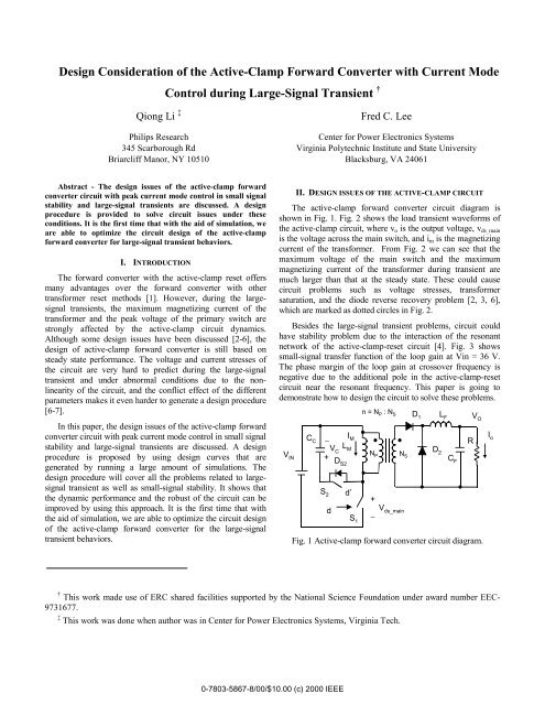
<strong>Design</strong> <strong>Consideration</strong> <strong>of</strong> <strong>the</strong> <strong>Active</strong>-<strong>Clamp</strong> <strong>Forward</strong> <strong>Converter</strong> with Current ModeControl during Large-Signal Transient †Qiong Li ‡Philips Research345 Scarborough RdBriarcliff Manor, NY 10510Fred C. LeeCenter for Power Electronics SystemsVirginia Polytechnic Institute and State UniversityBlacksburg, VA 24061Abstract - The design issues <strong>of</strong> <strong>the</strong> active-clamp forwardconverter circuit with peak current mode control in small signalstability and large-signal transients are discussed. A designprocedure is provided to solve circuit issues under <strong>the</strong>seconditions. It is <strong>the</strong> first time that with <strong>the</strong> aid <strong>of</strong> simulation, weare able to optimize <strong>the</strong> circuit design <strong>of</strong> <strong>the</strong> active-clampforward converter for large-signal transient behaviors.I. INTRODUCTIONThe forward converter with <strong>the</strong> active-clamp reset <strong>of</strong>fersmany advantages over <strong>the</strong> forward converter with o<strong>the</strong>rtransformer reset methods [1]. However, during <strong>the</strong> largesignaltransients, <strong>the</strong> maximum magnetizing current <strong>of</strong> <strong>the</strong>transformer and <strong>the</strong> peak voltage <strong>of</strong> <strong>the</strong> primary switch arestrongly affected by <strong>the</strong> active-clamp circuit dynamics.Although some design issues have been discussed [2-6], <strong>the</strong>design <strong>of</strong> active-clamp forward converter is still based onsteady state performance. The voltage and current stresses <strong>of</strong><strong>the</strong> circuit are very hard to predict during <strong>the</strong> large-signaltransient and under abnormal conditions due to <strong>the</strong> nonlinearity<strong>of</strong> <strong>the</strong> circuit, and <strong>the</strong> conflict effect <strong>of</strong> <strong>the</strong> differentparameters makes it even harder to generate a design procedure[6-7].In this paper, <strong>the</strong> design issues <strong>of</strong> <strong>the</strong> active-clamp forwardconverter circuit with peak current mode control in small signalstability and large-signal transients are discussed. A designprocedure is proposed by using design curves that aregenerated by running a large amount <strong>of</strong> simulations. Thedesign procedure will cover all <strong>the</strong> problems related to largesignaltransient as well as small-signal stability. It shows that<strong>the</strong> dynamic performance and <strong>the</strong> robust <strong>of</strong> <strong>the</strong> circuit can beimproved by using this approach. It is <strong>the</strong> first time that with<strong>the</strong> aid <strong>of</strong> simulation, we are able to optimize <strong>the</strong> circuit design<strong>of</strong> <strong>the</strong> active-clamp forward converter for <strong>the</strong> large-signaltransient behaviors.II. DESIGN ISSUES OF THE ACTIVE-CLAMP CIRCUITThe active-clamp forward converter circuit diagram isshown in Fig. 1. Fig. 2 shows <strong>the</strong> load transient waveforms <strong>of</strong><strong>the</strong> active-clamp circuit, where v o is <strong>the</strong> output voltage, v ds_mainis <strong>the</strong> voltage across <strong>the</strong> main switch, and i m is <strong>the</strong> magnetizingcurrent <strong>of</strong> <strong>the</strong> transformer. From Fig. 2 we can see that <strong>the</strong>maximum voltage <strong>of</strong> <strong>the</strong> main switch and <strong>the</strong> maximummagnetizing current <strong>of</strong> <strong>the</strong> transformer during transient aremuch larger than that at <strong>the</strong> steady state. These could causecircuit problems such as voltage stresses, transformersaturation, and <strong>the</strong> diode reverse recovery problem [2, 3, 6],which are marked as dotted circles in Fig. 2.Besides <strong>the</strong> large-signal transient problems, circuit couldhave stability problem due to <strong>the</strong> interaction <strong>of</strong> <strong>the</strong> resonantnetwork <strong>of</strong> <strong>the</strong> active-clamp-reset circuit [4]. Fig. 3 showssmall-signal transfer function <strong>of</strong> <strong>the</strong> loop gain at Vin = 36 V.The phase margin <strong>of</strong> <strong>the</strong> loop gain at crossover frequency isnegative due to <strong>the</strong> additional pole in <strong>the</strong> active-clamp-resetcircuit near <strong>the</strong> resonant frequency. This paper is going todemonstrate how to design <strong>the</strong> circuit to solve <strong>the</strong>se problems.C CI Mn = N P : N SD 1D 2L F V O_RV LV C MNP N IN +SD CS2FS 2 d’+dV ds_main_S 1Fig. 1 <strong>Active</strong>-clamp forward converter circuit diagram.I o† This work made use <strong>of</strong> ERC shared facilities supported by <strong>the</strong> National Science Foundation under award number EEC-9731677.‡ This work was done when author was in Center for Power Electronics Systems, Virginia Tech.0-7803-5867-8/00/$10.00 (c) 2000 IEEE
v oi mVin = 36 V, Io = 5 - 30 Av ds_main2 V/div100 V/divload to no load transient. Comparing <strong>the</strong> measurement andsimulation, it shows that <strong>the</strong> simulation is accurate enough toprovide <strong>the</strong> design information and predict <strong>the</strong> dynamicbehavior <strong>of</strong> <strong>the</strong> system.Time (s)1 A/divFig. 2 <strong>Active</strong>-clamp circuit problems during large-signaltransient.f (Hz)Vin = 36 V20 dB/div0 dB0 deg90 deg/divFig. 3 Stability problem due to <strong>the</strong> resonant network <strong>of</strong><strong>the</strong> active-clamp reset circuit.III. CIRCUIT UNDER WORST CASE CONDITIONThe fist step before we start <strong>the</strong> design is to find <strong>the</strong> worstcase condition during large-signal transient, so we can design<strong>the</strong> circuit under worst case condition. A virtual prototype testprocedure is used to detect <strong>the</strong> circuit worst case condition bysimulating <strong>the</strong> circuit dynamic performance under differentlines, loads, and <strong>the</strong> abnormal conditions [7].An active-clamp forward converter circuit with peakcurrent mode control is used as an example to demonstrate <strong>the</strong>design process. The circuit has input voltage 36 - 72 V and fullload 30 A. The duty cycle limit <strong>of</strong> <strong>the</strong> controller chip is 0.75.The control bandwidth <strong>of</strong> <strong>the</strong> current circuit design is 14 kHz.From <strong>the</strong> simulation, it shows that <strong>the</strong> worst condition occurswhen <strong>the</strong> circuit has a large load transient from no load to fullload at low line.In order to verify <strong>the</strong> accuracy <strong>of</strong> simulation, a circuitprototype was built to compare <strong>the</strong> circuit dynamicperformance. Fig. 4 shows <strong>the</strong> large-signal responsewaveforms at Vin = 36 V, Io from no load to full load to noload transient. The load step slew rate is 1 A/us. Fig. 4(a) is <strong>the</strong>measured waveform from no load to full load transient. Fig.4(b) is <strong>the</strong> simulated waveform from no load to full loadtransient. Fig. 4(c) is <strong>the</strong> measured waveform from full load tono load transient. Fig. 4(d) is <strong>the</strong> simulated waveform from fullIV. DESIGN PROCEDURE OF THE ACTIVE-CLAMP CIRCUITAlthough it is possible to adjust <strong>the</strong> circuit parameters bytrials and errors to fix <strong>the</strong> problems, <strong>the</strong> problem's solution isnot straightforward. It may require a lot <strong>of</strong> time and effort butstill not come out a robust design, since <strong>the</strong>se parameters arenot independent parameters and involve different circuit designissues.This section will demonstrate how to generate designinformation and optimize <strong>the</strong> design parameters related to <strong>the</strong>sedesign issues. The design parameters discussed here are <strong>the</strong>magnetizing inductance <strong>of</strong> <strong>the</strong> transformer L m , <strong>the</strong> clampcapacitance C c , <strong>the</strong> control bandwidth f c , and <strong>the</strong> maximumduty cycle limit Dmax. The design process focuses on solving<strong>the</strong> potential problems in <strong>the</strong> circuit: voltage stress <strong>of</strong> <strong>the</strong> mainswitch, transformer core saturation, diode reverse recovery <strong>of</strong><strong>the</strong> active-clamp switch, small-signal instability due to <strong>the</strong>active-clamp resonant network.A. NormalizationThe normalized peak voltage and peak current values willbe used in <strong>the</strong> design curve. The normalized switch voltage isVsand <strong>the</strong> normalized magnetizing current isV minin( )im⋅ Zo. The x-axis <strong>of</strong> <strong>the</strong> design curve uses resonantVin( min)frequency, f o as a parameter, and Z o is <strong>the</strong> character impedance.fo1=2 ⋅π⋅ Lcm⋅ Cc(1)LmZ o = (2)CB. <strong>Design</strong> constraintsThere are four design criteria: <strong>the</strong> voltage stress <strong>of</strong> <strong>the</strong> mainswitch, <strong>the</strong> transformer saturation, <strong>the</strong> reverse recoveryproblem <strong>of</strong> <strong>the</strong> body diode <strong>of</strong> <strong>the</strong> active clamp switch, and <strong>the</strong>small-signal stability problem.♦ <strong>Design</strong> constraint 1: switch voltage stressThe design constraint for <strong>the</strong> switch voltage stress is:V s (peak) < V s (rating) (3)Where, V s (peak) is <strong>the</strong> peak voltage during <strong>the</strong> transient,V s (rating) is <strong>the</strong> device voltage rating <strong>of</strong> <strong>the</strong> main switch.0-7803-5867-8/00/$10.00 (c) 2000 IEEE
MeasurementSimulationVds_main50 V/div50 V/divIo30 A/div40 A/divTime (2.5 us/div)(a)MeasurementTime (s)(b)SimulationVds_main50 V/div50 V/divIo30 A/div40 A/divTime (10 us/div)(c)Time (s)Fig. 4. Large-signal response waveforms at Vin = 36 V, Io from no load to full load to no load transient. Load step slew rateis 1 A/us. (a) measured waveform <strong>of</strong> no load to full load transient. (b) simulated waveform <strong>of</strong> no load to full load transient.(c) measured waveform <strong>of</strong> full load to no load transient. (d) simulated waveform <strong>of</strong> full load to no load transient.♦ <strong>Design</strong> constraint 2: small signal stabilityThe resonant frequency <strong>of</strong> <strong>the</strong> active-clamp circuit shouldmeet <strong>the</strong> following equation in order to have a stable systemand not affect <strong>the</strong> phase margin.2⋅f cfo> (4)d' limwhere d' lim is <strong>the</strong> duty cycle limit value <strong>of</strong> <strong>the</strong> controllerchip, f c is <strong>the</strong> control bandwidth.♦ <strong>Design</strong> constraint 3: transformer saturationFig.5 shows <strong>the</strong> relation between <strong>the</strong> flux and <strong>the</strong>magnetizing current, where, A e is <strong>the</strong> effective cross sectionalarea <strong>of</strong> <strong>the</strong> core, Lm is <strong>the</strong> magnetizing current. From Fig.5, wecan get:im( sat)(d)Bsat⋅ Ae⋅ Np= (5)LmWe can rewrite saturating magnetizing current into:Bsat⋅ Ae⋅ Np⋅ 2 ⋅π⋅ foim( sat)=(6)ZoThe design constraint for transformer saturation is:im( peak)⋅ Z Bsat⋅ Ae⋅ Np⋅ 2o
Φ5.0Bsat⋅ A ei m( sat )ΦN ⋅ ipmL=Nm2pNp⋅imIm(peak)*Zo/Vin(min)4.03.02.01.0Diode reverserecovery problemareaim( peak)⋅ Zon ⋅Vo⋅ 2 ⋅=Vin( min) fs⋅ Zoπ ⋅ foFig.5. Relation <strong>of</strong> <strong>the</strong> saturation flux to <strong>the</strong> saturationmagnetizing current.5.00.00.0E+00 1.0E+05 2.0E+05 3.0E+05 4.0E+05 5.0E+05 6.0E+05fo (Hz)Fig.7. The diode reverse recovery problem area.Im(peak)*Zo/Vin(min)4.03.02.01.0transformersaturation areaim( peak)⋅ Z Bsat⋅ Ae⋅ Np⋅ 2o=V ( min) V ( min)in0.00.0E+00 1.0E+05 2.0E+05 3.0E+05 4.0E+05 5.0E+05 6.0E+05fo (Hz)in⋅π⋅ foVs(peak)/Vin(min)6.05.04.03.02.01.0Small-signal unstable areaVoltage overstress area<strong>Design</strong> area forvoltage curveFig. 6 The transformer saturation area.The design constraint for <strong>the</strong> transformer saturation isshown as shaded area in Fig. 6. It is a straight line in <strong>the</strong>normalized design curve.♦ <strong>Design</strong> constraint 4: diode reverse recovery problemThe magnetizing current to prevent <strong>the</strong> diode from reverserecovery problem is:im ( peak) < im( ripple)(8)where,im( ripple)V⋅ D ⋅Tn ⋅V⋅Tin so s= =( 9)LmLmThe ripple current can be written as:im( ripple)⋅ Zon ⋅Vo⋅ 2 ⋅π⋅ f=V ( min) f ⋅V( min)insino(10)The diode reverse recovery problem area is shown as inFig.7. It is a straight line in <strong>the</strong> normalized design curve.According to four design constraints, we can draw <strong>the</strong>feasible operating regions for voltage and magnetizing currentas shown in Fig.8.Im(peak)*Zo/Vin(min)0.00.0E+00 1.0E+05 2.0E+05 3.0E+05 4.0E+05 5.0E+05 6.0E+055.04.03.02.01.0Small-signal unstable areafo (Hz)(a)Transformersaturation areaDiode reverserecovery problem area<strong>Design</strong> area for currentcurve0.00.0E+00 1.0E+05 2.0E+05 3.0E+05 4.0E+05 5.0E+05 6.0E+05fo (Hz)(b)Fig.8 Feasible operating regions for voltage andmagnetizing current. (a) design area for normalizedswitch voltage curve. (b) design area for normalizedmagnetizing current curve.C. Generating design curvesThe worst case happens at low line and load from low tohigh transient. In this example, Vin is 36 V, and Io changesfrom 0 A to 30 A. A set <strong>of</strong> design curves is generated by0-7803-5867-8/00/$10.00 (c) 2000 IEEE
varying L m and C c values with a fixed control bandwidth, 14kHz, and maximum duty cycle limit, 0.75. Each singlesimulation generates one point in <strong>the</strong> voltage design curve andone point in <strong>the</strong> magnetizing current curve. The normalizeddesign curve for peak voltage and magnetizing current areshown in Fig. 9 and Fig. 10, respectively. The shaded areas are<strong>the</strong> design prohibited area. The total simulation CPU time isonly 9 minutes by using an adequate simulation and modelingapproach [7].D. The feasible Lm and Cc to meet <strong>the</strong> design constraintsAfter we generate <strong>the</strong> design curves with designconstraints, <strong>the</strong> feasible L m and C c to meet all <strong>the</strong> designcriteria can be easily determined.Assuming <strong>the</strong> device rating <strong>of</strong> <strong>the</strong> main switch is 180 V, so<strong>the</strong> normalized boundary <strong>of</strong> <strong>the</strong> voltage stress is 5 whenV in (min) = 36 V. When <strong>the</strong> control bandwidth, f c = 14 kHz, andmaximum duty cycle limit, d lim = 0.75, <strong>the</strong> boundary <strong>of</strong> <strong>the</strong>resonant frequency for small-signal stability is 112 kHz. Thefeasible L m and C c can be determined by three steps.1. Find <strong>the</strong> desired parameter ranges for f o and L m in peakvoltagedesign curves.Fig. 9 is <strong>the</strong> peak-voltage design curves with f c 14 kHz andd lim 0.75. These is a big dot in Fig. 9, which corresponds to <strong>the</strong>original design, L m = 80 uH and C c = 0.01 uF. The maximumvoltage is about 200 V, so <strong>the</strong> original design exceeds <strong>the</strong> 180V voltage rating <strong>of</strong> <strong>the</strong> switch under worst case condition.The dotted lines covered area is <strong>the</strong> desired design area tomeet voltage stress limitation and small signal stable criterionin <strong>the</strong> normalized peak switch voltage vs. f o curves. We can seethat only <strong>the</strong> curve at L m = 20 uH meets <strong>the</strong> constraints whenf o is at 112 kHz to 480 k Hz range.2. Within <strong>the</strong> defined ranges for f o and L m in step 1, we canfind <strong>the</strong> desired ranges for f o and L m that also meet <strong>the</strong>magnetizing current constraints.Fig. 10 is <strong>the</strong> peak magnetizing-current design curves withf c 14 kHz and d lim 0.75. These is a big dot in Fig. 10, whichcorresponds to <strong>the</strong> original design, L m = 80 uH and C c = 0.01uF. It shows that <strong>the</strong> original design has diode reverse recoveryproblem and is at <strong>the</strong> boundary <strong>of</strong> <strong>the</strong> transformer saturation.From <strong>the</strong> design curves, we can see that <strong>the</strong>re are n<strong>of</strong>easible parameters available within <strong>the</strong> desired areas fromstep1. It also means that <strong>the</strong>re is no feasible L m and C c canmeet all <strong>the</strong> design constraints in <strong>the</strong> previous circuit condition.3. If we find <strong>the</strong> desired ranges for f o and L m from step 1and 2, C c can be calculated byCc=12( 2 ⋅π⋅ fo) ⋅ Lm(11)Within <strong>the</strong> desired parameter range, a smaller f o , thus asmaller C c is preferred to reduce <strong>the</strong> voltage and currentstresses.Vs(peak)/Vin(min)6.05.04.03.02.01.0small signal unstable areaVoltage overstress areaLm = 160 uHLm = 320 uHLm = 80 uH<strong>Design</strong> areaLm = 40 uHLm = 20 uH0.00.0E+00 1.0E+05 2.0E+05 3.0E+05 4.0E+05 5.0E+05 6.0E+05fo (Hz)Fig. 9 <strong>Design</strong> curve <strong>of</strong> <strong>the</strong> normalized peak switch voltagevs. f o .Im(peak)*Zo/Vin(min)5.04.03.02.01.0small signal unstable areatransformer saturationareaLm = 160 uHLm = 320 uHDiode reverserecovery areaLm = 80 uHLm = 40 uHLm = 20 uH0.00.0E+00 1.0E+05 2.0E+05 3.0E+05 4.0E+05 5.0E+05 6.0E+05fo (Hz)Fig. 10 <strong>Design</strong> curve <strong>of</strong> normalized peak magnetizingcurrent vs. f o .V. DESIGN TRADE-OFFPrevious example shows that <strong>the</strong>re is no adequate L m andC c to meet all <strong>the</strong> design criteria. There are several designtrade-<strong>of</strong>f to solve <strong>the</strong> problem.A. <strong>Design</strong> trade-<strong>of</strong>f 1: increasing device ratingFrom Fig. 9 and Fig. 10, we see that if we do not restrict<strong>the</strong> device voltage rating to 180 V, <strong>the</strong>re is a small area in Fig.10 which can meet all <strong>the</strong> design criteria with Lm = 20 uH. Thedisadvantages <strong>of</strong> this solution are <strong>the</strong> higher voltage ratingdevice and <strong>the</strong> high ripple current <strong>of</strong> <strong>the</strong> magnetizing currentdue to a small L m .It is worthwhile to mention that a very small magnetizinginductance could have a high ripple <strong>of</strong> <strong>the</strong> magnetizing currentwhich will increase <strong>the</strong> loss <strong>of</strong> <strong>the</strong> circuit and may affect <strong>the</strong>0-7803-5867-8/00/$10.00 (c) 2000 IEEE
main converter operation if <strong>the</strong> ripple <strong>of</strong> <strong>the</strong> magnetizingcurrent is not negligible to <strong>the</strong> reflected load.B. <strong>Design</strong> trade-<strong>of</strong>f 2: getting rid <strong>of</strong> <strong>the</strong> constraint <strong>of</strong> <strong>the</strong>body diode reverse recoveryFrom Fig. 10, we see that <strong>the</strong> diode reverse recoveryconstraint is <strong>the</strong> hardest one to meet in <strong>the</strong> parameter design.The design is more flexible without this constraint. This can bedone by connecting a Schottky diode in series with <strong>the</strong>auxiliary switch to block <strong>the</strong> conduction <strong>of</strong> <strong>the</strong> body diode, and<strong>the</strong>n to connect a fast-recovery anti-parallel diode around <strong>the</strong>series connection <strong>of</strong> <strong>the</strong> Schottky and <strong>the</strong> auxiliary switch [56].The disadvantage is <strong>the</strong> additional components to increase <strong>the</strong>cost <strong>of</strong> <strong>the</strong> circuit.C. <strong>Design</strong> trade-<strong>of</strong>f 3: decreasing control bandwidthA smaller bandwidth in <strong>the</strong> design can reduce <strong>the</strong> peakvoltage and current during load transients. The disadvantage isa slower recovery from transient in <strong>the</strong> output voltage <strong>of</strong> <strong>the</strong>main converter.D. <strong>Design</strong> trade-<strong>of</strong>f 4: reducing maximum duty cycle limitvalueThe voltage and current stresses can also be reduced byreducing <strong>the</strong> maximum duty cycle limit value. Similar tosolution 3, <strong>the</strong> disadvantage is a slower recovery from transientin <strong>the</strong> output voltage <strong>of</strong> <strong>the</strong> main converter.E. Circuit redesign by using trade-<strong>of</strong>f 4We will use design trade-<strong>of</strong>f 4 as an example to show <strong>the</strong>circuit redesign result. The design procedure is <strong>the</strong> same as in<strong>the</strong> previous section.Fig.11 and Fig.12 shows <strong>the</strong> normalized voltage designcurve with reduced maximum duty cycle limit. The maximumduty cycle limit is reduced from 0.75 to 0.7. The design resultis L m = 40 uH, C c is less than 0.011 uF. A smaller C c has alarger voltage stress, but less current stress and more designmargin without saturation and diode reverse recovery problem.VI. VALIDATION OF THE DESIGN BY VIRTUAL PROTOTYPETESTFig. 15 shows <strong>the</strong> comparisons between <strong>the</strong> original circuitproblems and <strong>the</strong> circuit behavior after <strong>the</strong> final designmodification. The circuit parameters are modified by reducing<strong>the</strong> maximum duty cycle limit from 0.75 to 0.7 andmagnetizing inductance from 80 uH to 40 uH. The clampcapacitance is 0.01 uF.Fig. 13 shows design verification <strong>of</strong> dc bias <strong>of</strong> magnetizingcurrent <strong>of</strong> transformer. The dc bias <strong>of</strong> <strong>the</strong> magnetizing currentdoes not shown any problems since <strong>the</strong> magnetizing currentripple is about 800 mA.Vs(peak)/Vin(min)6.05.04.03.02.01.0small signal unstable areaVoltage overstress areaLm = 160 uHLm = 40 uHLm = 80 uHLm = 20 uHLm = 320 uH<strong>Design</strong> area0.00.0E+00 1.0E+05 2.0E+05 3.0E+05 4.0E+05 5.0E+05 6.0E+05fo (Hz)Fig.11 Normalized voltage design curve reducedmaximum duty cycle limit. The Dlim is reduced from0.75 to 0.7. The design area to meet voltage stresslimitation and small signal stable criteria is shown in <strong>the</strong>dotted area.Im(peak)*Zo/Vin(min)5.04.03.02.01.0small signal unstable areaDiode reversetransformer saturationrecovery boundaryboundaryLm = 320 uHLm = 80 uHLm = 40 uH<strong>Design</strong> area forL m= 40 uH0.00.0E+00 1.0E+05 2.0E+05 3.0E+05 4.0E+05 5.0E+05 6.0E+05fo (Hz)Fig.12 Normalized magnetizing current design curve withreduced maximum duty cycle limit. The Dlim is reducedfrom 0.75 to 0.7. The design area without transformersaturation and diode reverse recovery problem shows in<strong>the</strong> dotted line.Fig. 14 shows <strong>the</strong> design verification <strong>of</strong> <strong>the</strong> small signalanalysis under worst case condition. The resonant frequency <strong>of</strong><strong>the</strong> active-clamp circuit has been pushed high enough and doesnot interfere with <strong>the</strong> crossover frequency <strong>of</strong> <strong>the</strong> loop gain.0-7803-5867-8/00/$10.00 (c) 2000 IEEE
Vin = 36 VVin = 48 V100 V/divIm (A)Vin = 72 V0.5 A/div40 A/divIo (A)Fig. 13. <strong>Design</strong> verification <strong>of</strong> dc bias <strong>of</strong> magnetizingcurrent <strong>of</strong> transformer at steady state.20 dB/divVin = 36 Vv ds_mainTime (s)(a)100 V/div0 dB0 deg0.5 A/divi oi m(b)40 A/div90 deg/divTime (s)Fig. 14 <strong>Design</strong> verification <strong>of</strong> <strong>the</strong> small signal analysis.Fig. 15 shows <strong>the</strong> design verification <strong>of</strong> <strong>the</strong> large-signaltransient analysis under worst case: Vin = 36 V, Io = 0 to 30 A.Fig. 15(a) shows <strong>the</strong> waveforms with original design. Fig.15(b) shows <strong>the</strong> waveforms after design modification. Theoriginal circuit problems during large-signal transient aresolved.VII.CONCLUSIONSThe design issues <strong>of</strong> <strong>the</strong> active-clamp forward convertercircuit with peak current mode control in small signal stabilityand large-signal transients are discussed. A design procedure isproposed to solve design issues. The circuit performances <strong>of</strong><strong>the</strong> power supply system design are improved by redesign <strong>the</strong>active-clamp reset circuit. It is <strong>the</strong> first time that with <strong>the</strong> aid <strong>of</strong><strong>the</strong> virtual prototype, we are able to optimize <strong>the</strong> circuit design<strong>of</strong> <strong>the</strong> active-clamp forward converter for large-signal transientbehaviors.Fig. 15 <strong>Design</strong> verification <strong>of</strong> <strong>the</strong> large-signal transientanalysis with worst case: Vin = 36 V, Io = 0 to 30 A. (a)waveforms with original design. (b) waveforms afterdesign modification.REFERENCES[1] P. Vinciarelli, “Optimal resetting <strong>of</strong> <strong>the</strong> transformer’s core in singleended forward converters,” U.S. Patent, No. 4,441,146, Apr. 1984.[2] B. Carsten, “<strong>Design</strong> techniques for transformer active reset circuits athigh frequencies and power levels,” HFPC Conf. Proc., pp.235-246,1990.[3] D. Dalal and L. W<strong>of</strong>ford, “Novel control IC for single-ended activeclamp converters,” HFPC Conf. Proc., pp. 136-146, 1995.[4] Q. Li, F. C. Lee, and M. M. Jovanovic, “<strong>Design</strong> considerations <strong>of</strong>transformer DC bias <strong>of</strong> forward converter with active-clamp reset,”IEEE APEC Proc., pp.553-559, March 14-18, 1999.[5] A. Fontan, S. Ollero, E. de la Cruz, and J. Sebastian, “Peak currentmode control applied to <strong>the</strong> forward converter with active clamp,”IEEE PESC Rec., pp. 45-51, 1998.[6] Q. Li, F. C. Lee, and M. M. Jovanovic, “Large-signal transient analysis<strong>of</strong> forward converter with active-clamp reset,” IEEE PESC Rec.,pp.633-639, May 1998.[7] Q. Li, “Developing Modeling and simulation methodology for virtualprototype power supply system,” Ph.D Dissertation, CPES, VPI&SU,March 1999.0-7803-5867-8/00/$10.00 (c) 2000 IEEE