

MC1377 Color Television RGB to PAL/NTSC Encoder
MC1377 Color Television RGB to PAL/NTSC Encoder
MC1377 Color Television RGB to PAL/NTSC Encoder

Create successful ePaper yourself
Turn your PDF publications into a flip-book with our unique Google optimized e-Paper software.
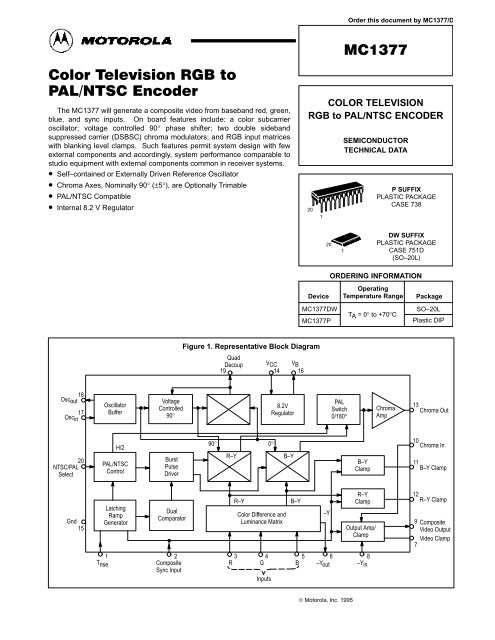
Order this document by <strong>MC1377</strong>/D The <strong>MC1377</strong> will generate a composite video from baseband red, green,blue, and sync inputs. On board features include: a color subcarrieroscilla<strong>to</strong>r; voltage controlled 90° phase shifter; two double sidebandsuppressed carrier (DSBSC) chroma modula<strong>to</strong>rs; and <strong>RGB</strong> input matriceswith blanking level clamps. Such features permit system design with fewexternal components and accordingly, system performance comparable <strong>to</strong>studio equipment with external components common in receiver systems.• Self–contained or Externally Driven Reference Oscilla<strong>to</strong>r• Chroma Axes, Nominally 90° (±5°), are Optionally Trimable• <strong>PAL</strong>/<strong>NTSC</strong> Compatible• Internal 8.2 V Regula<strong>to</strong>rCOLOR TELEVISION<strong>RGB</strong> <strong>to</strong> <strong>PAL</strong>/<strong>NTSC</strong> ENCODER201SEMICONDUCTORTECHNICAL DATAP SUFFIXPLASTIC PACKAGECASE 738201DW SUFFIXPLASTIC PACKAGECASE 751D(SO–20L)ORDERING INFORMATIONDevice<strong>MC1377</strong>DW<strong>MC1377</strong>POperatingTemperature RangeTA = 0° <strong>to</strong> +70°CPackageSO–20LPlastic DIPFigure 1. Representative Block DiagramQuadDecoup VCC VB19 14 1618Oscout17OscinOscilla<strong>to</strong>rBufferVoltageControlled90°8.2VRegula<strong>to</strong>r<strong>PAL</strong>Switch0/180°ChromaAmp13Chroma Out20<strong>NTSC</strong>/<strong>PAL</strong>SelectH/2<strong>PAL</strong>/<strong>NTSC</strong>ControlBurstPulseDriver90° 0°R–YB–YB–YClamp10Chroma In11B–Y ClampGnd15LatchingRampGenera<strong>to</strong>rDualCompara<strong>to</strong>r<strong>Color</strong> Difference andLuminance MatrixR–YClampOutput Amp/Clamp1 2 3 4 5 6 8InputsTriseCompositeSync InputR G B –Yout–YinR–YB–Y–Y12R–Y Clamp97CompositeVideo OutputVideo Clamp© Mo<strong>to</strong>rola, Inc. 1995MOTOROLA ANALOG IC DEVICE DATA1
MAXIMUM OPERATING CONDITIONS<strong>MC1377</strong>Rating Symbol Value UnitSupply Voltage VCC 15 VdcS<strong>to</strong>rage Temperature Tstg –65 <strong>to</strong> +150 °CPower Dissipation PackageDerate above 25°CPD 1.2510WmW/°COperating Temperature TA 0 <strong>to</strong> +70 °CRECOMMENDED OPERATING CONDITIONSCharacteristics Min Typ Max UnitSupply Voltage 10 12 14 VdcIB Current (Pin 16) 0 – –10 mASync, Blanking Level (DC level between pulses, see Figure 9e)Sync Tip Level (see Figure 9e)Sync Pulse Width (see Figure 9e)1.7–0.52.5–0–8.20.95.2VdcµsR, G, B Input (Amplitude)R, G, B Peak Levels for DC Coupled Inputs, with Respect <strong>to</strong> Ground–2.21.0––4.4VppVChrominance Bandwidth (Non–comb Filtered Applications), (6 dB) 0.5 1.5 2.0 MHzExt. Subscarrier Input (<strong>to</strong> Pin 17) if On–Chip Oscilla<strong>to</strong>r is not used. 0.5 0.7 1.0 VppELECTRICAL CHARACTERISTICS (VCC = 12 Vdc, TA = 25°C, circuit of Figure 7, unless otherwise noted.)Characteristics Pins Symbol Min Typ Max UnitSUPPLY CURRENTSupply Current in<strong>to</strong> VCC, No Load, on Pin 9.Circuit Figure 7VCC = 10 VVCC = 11 VVCC = 12 VVCC = 13 VVCC = 14 V14 ICC ––20––3334353637––40––mAVOLTAGE REGULATORVB Voltage (IB = –10 mA, VCC = 12 V, Figure 7)Load Regulation (0 < IB ≤ 10 mA, VCC = 12 V)Line Regulation (IB = 0 mA, 10 V < VCC < 14 V) ≤16 VBRegloadRegline7.7–20–8.21204.58.7+30–VdcmVmV/VOSCILLATOR AND MODULATIONOscilla<strong>to</strong>r Amplitude with 3.58 MHz/4.43 MHz crystal 17 Osc – 0.6 – VppSubcarrier Input: Resistance at 3.58 MHzSubcarrier Input: Resistance at 4.43 MHz17 Rosc ––5.04.0––kΩCapacitance Cosc – 2.0 – pFModulation Angle (R–Y) <strong>to</strong> (B–Y)Angle Adjustment (R–Y)DC Bias Voltage–1919∅m∆∅mV19–––±50.256.4–––DegDeg/µAVdcCHROMINANCE AND LUMINANCEChroma Input DC LevelChroma Input Level for 100% Saturation10 Vin ––4.00.7––VdcVppChroma Input: ResistanceChroma Input: CapacitanceRinCin––102.0––kΩpFChroma DC Output LevelChroma Output Level at 100% Saturation13 Vout 8.9–101.010.9–VdcVppChroma Output Resistance Rout – 50 – ΩLuminance Bandwidth (–3.0 dB), Less Delay Line 9 BWLuma – 8.0 – MHz2 MOTOROLA ANALOG IC DEVICE DATA
<strong>MC1377</strong>ELECTRICAL CHARACTERISTICS (VCC = 12 Vdc, TA = 25°C, circuit of Figure 7, unless otherwise noted.)Characteristics Pins Symbol Min Typ Max UnitVIDEO INPUTR, G, B Input DC Levels 3, 4, 5 <strong>RGB</strong> 2.8 3.3 3.8 VdcR, G, B Input for 100% <strong>Color</strong> Saturation – 1.0 – VppR, G, B Input: ResistanceR, G, B Input: CapacitanceR<strong>RGB</strong>C<strong>RGB</strong>8.0–102.017–kΩpFSync Input Resistance (1.7 V < Input < 8.2) 2 Sync – 10 – kΩCOMPOSITE VIDEO OUTPUTComposite Output,100% Saturation(see Figure 8d)SyncLuminanceChromaBurst9 CVout ––––0.61.41.70.6––––VppOutput Impedance (Note 1) Rvideo – 50 – ΩSubcarrier Leakage in Output (Note 2) Vlk – 20 – mVppNOTES: 1. Output Impedance can be reduced <strong>to</strong> less than 10 Ω by using a 150 Ω output load from Pin 9 <strong>to</strong> ground. Power supply current willincrease <strong>to</strong> about 60 mA.2. Subcarrier leakage can be reduced <strong>to</strong> less than 10 mV with optional circuitry (see Figure 12).Symbol Pin DescriptionPIN FUNCTION DESCRIPTIONStr 1 External components at this pin set the rise time of the internal ramp function genera<strong>to</strong>r (see Figure 10).Sync 2 Composite sync input. Presents 10 kΩ resistance <strong>to</strong> input.R 3 Red signal input. Presents 10 kΩ impedance <strong>to</strong> input. 1.0 Vpp required for 100% saturation.G 4 Green signal input. Presents 10 kΩ impedance <strong>to</strong> input. 1.0 Vpp required for 100% saturation.B 5 Blue signal Input. Presents 10 kΩ impedance <strong>to</strong> input. 1.0 Vpp required for 100% saturation.–Yout 6 Luma (–Y) output. Allows external setting of luma delay time.Vclamp 7 Video Clamp pin. Typical connection is a 0.01 µF capaci<strong>to</strong>r <strong>to</strong> ground.–Yin 8 Luma (–Y) input. Presents 10 kΩ input impedance.CVout 9 Composite Video output. 50 Ω output impedance.ChromaIn 10 Chroma input. Presents 10 kΩ input impedance.B–Yclamp 11 B–Y clamp. Clamps B–Y during blanking with a 0.1 µF capaci<strong>to</strong>r <strong>to</strong> ground.Also used with R–Y clamp <strong>to</strong> null residual color subcarrier in output.R–Yclamp 12 R–Y clamp. Clamps R–Y during blanking with a 0.1 µF capaci<strong>to</strong>r <strong>to</strong> ground.Also used with B–Y clamp <strong>to</strong> null residual color subcarrier in output.ChromaOut 13 Chroma output. 50 Ω output impedance.VCC 14 Power supply pin for the IC; +12, ±2.0 V, required at 35 mA (typical).Gnd 15 Ground pin.VB 16 8.2 V reference from an internal regula<strong>to</strong>r capable of delivering 10 mA <strong>to</strong> external circuitry.Oscin 17 Oscilla<strong>to</strong>r input. A transis<strong>to</strong>r base presents 5.0 kΩ <strong>to</strong> an external subcarrier input, or is available forconstructing a Colpitts oscilla<strong>to</strong>r (see Figure 4).Oscout 18 Oscilla<strong>to</strong>r output. The emitter of the transis<strong>to</strong>r, with base access at Pin 17, is accessible for completing theColpitts oscilla<strong>to</strong>r. See Figure 4.∅m 19 Quad decoupler. With external circuitry, R–Y <strong>to</strong> B–Y relative angle errors can be corrected. Typically,requires a 0.01 µF capaci<strong>to</strong>r <strong>to</strong> ground.<strong>NTSC</strong>/<strong>PAL</strong>Select20 <strong>NTSC</strong>/<strong>PAL</strong> switch. When grounded, the <strong>MC1377</strong> is in the <strong>NTSC</strong> mode; if unconnected, in the <strong>PAL</strong> mode.MOTOROLA ANALOG IC DEVICE DATA3
<strong>MC1377</strong><strong>Color</strong> Reference Oscilla<strong>to</strong>r/BufferAs stated earlier in the general description, there is anon–board common collec<strong>to</strong>r Colpitts color referenceoscilla<strong>to</strong>r with the transis<strong>to</strong>r base at Pin 17 and the emitter atPin 18. When used with a common low–cost TV crystal andcapacitive divider, about 0.6 Vpp will be developed at Pin 17.The frequency adjustment can be done with a series 30 pFtrimmer capaci<strong>to</strong>r over a <strong>to</strong>tal range of about 1.0 kHz.Oscilla<strong>to</strong>r frequency should be adjusted for each unit,keeping in mind that most moni<strong>to</strong>rs and receivers can pull in1200 Hz.If an external color reference is <strong>to</strong> be used exclusively, itmust be continuous. The components on Pins 17 and 18 canbe removed, and the external source capacitively coupledin<strong>to</strong> Pin 17. The input at Pin 17 should be a sine wave withamplitude between 0.5 Vpp and 1.0 Vpp.Also, it is possible <strong>to</strong> do both; i.e., let the oscilla<strong>to</strong>r “free run”on its own crystal and override with an external source. Anextra coupling capaci<strong>to</strong>r of 50 pF from the external source <strong>to</strong>Pin 17 was adequate with the experimentation attempted.Voltage Controlled 90°The oscilla<strong>to</strong>r drives the (B–Y) modula<strong>to</strong>r and a voltagecontrolled phase shifter which produces an oscilla<strong>to</strong>r phaseof 90° ±5° at the (R–Y) modula<strong>to</strong>r. In most situations, theresult of an error of 5° is very subtle <strong>to</strong> all but the most experteye. However, if it is necessary <strong>to</strong> adjust the angle <strong>to</strong> betteraccuracy, the circuit shown in Figure 11 can be used.Pulling Pin 19 up will increase the (R–Y) <strong>to</strong> (B–Y) angle byabout 0.25°/µA. Pulling Pin 19 down reduces the angle by thesame sensitivity. The nominal Pin 19 voltage is about 6.3 V,so even though it is unregulated, the 12 V supply is best forgood control. For effective adjustment, the simplest approachis <strong>to</strong> apply <strong>RGB</strong> color bar inputs and use a vec<strong>to</strong>rscope. Asimple bar genera<strong>to</strong>r giving R, G, and B outputs is shown inFigure 26.Figure 9. Ramp/Burst Gate Genera<strong>to</strong>r5.0Pin 1 Ramp Voltage(Vdc)1.31.00Burst S<strong>to</strong>pBurst StartSync(Pin 2)0 5.5 8.5Time (µs)50 63.5Residual Feedthrough ComponentsAs shown in Figure 9(d), the composite output at Pin 9for fully saturated color bars is about 2.6 Vpp, output with fullchroma on the largest bars (cyan and red) being 1.7 Vpp.The typical device, due <strong>to</strong> imperfections in gain, matrixing,and modula<strong>to</strong>r balance, will exhibit about 20 mVpp residualcolor subcarrier in both white and black. Both residuals canbe reduced <strong>to</strong> less than 10 mVpp for the more exactingapplications.The subcarrier feedthrough in black is due primarily <strong>to</strong>imbalance in the modula<strong>to</strong>rs and can be nulled by sinking orsourcing small currents in<strong>to</strong> clamp Pins 11 and 12 as shownin Figure 12. The nominal voltage on these pins is about4.0 Vdc, so the 8.2 V regula<strong>to</strong>r is capable of supplying a pullup source. Pulling Pin 11 down is in the 0° direction, pulling itup is <strong>to</strong>wards 180°. Pulling Pin 12 down is in the 90° direction,pulling it up is <strong>to</strong>wards 270°. Any direction of correction maybe required from part <strong>to</strong> part.White carrier imbalance at the output can only becorrected by juggling the relative levels of R, G, and B inputsfor perfect balance. Standard devices are tested <strong>to</strong> be within5% of balance at full saturation. Black balance should beadjusted first, because it affects all levels of gray scaleequally. There is also usually some residual baseband videoat the chroma output (Pin 13), which is most easily observedby disabling the color oscilla<strong>to</strong>r. Typical devices show 0.4 Vppof residual luminance for saturated color bar inputs. This isnot a major problem since Pin 13 is always coupled <strong>to</strong> Pin 10through a bandpass or a high pass filter, but it serves as awarning <strong>to</strong> pay proper attention <strong>to</strong> the coupling network.Figure 10. Adjusting Modula<strong>to</strong>r Angle12Vdc190.01µF220k10kMOTOROLA ANALOG IC DEVICE DATA9
<strong>MC1377</strong>Figure 11. Nulling Residual <strong>Color</strong> in BlackVB12 470k10k1110k470kVBFigure 12. Delay of Chroma InformationLuminanceChromaFigure 14(a) shows the output of the <strong>MC1377</strong> with lowresolution <strong>RGB</strong> inputs. If no bandwidth reduction is employedthen a moni<strong>to</strong>r or receiver with frequency response shown inFigure 14(b), which is fairly typical of non–comb filteredmoni<strong>to</strong>rs and receivers, will detect an incorrect lumasideband at X′. This will result in cross–talk in the form ofchroma information in the luma channel. To avoid thissituation, a simpler bandpass circuit as shown in Figure15(a), can be used.GainFigure 13. <strong>MC1377</strong> Output withLow Resolution <strong>RGB</strong> InputsX X X X1.0 2.0 3.0 3.58 4.0 5.0(a) <strong>Encoder</strong> Output with Low Resolution Inputsand No Bandpass TransformerThe Chroma Coupling CircuitsWith the exception of S–VHS equipped moni<strong>to</strong>rs andreceivers, it is generally true that most moni<strong>to</strong>rs and receivershave color IF 6.0 dB bandwidths limited <strong>to</strong> approximately±0.5 MHz. It is therefore recommended that the encodercircuit should also limit the chroma bandwidth <strong>to</strong>approximately ±0.5 MHz through insertion of a bandpasscircuit between Pin 13 and Pin 10. However, if S–VHSoperation is desired, a coupling circuit which outputs thecomposite chroma directly for connection <strong>to</strong> a S–VHSterminal is given in the S–VHS application (see Figure 19).For proper color level in the video output, a ±0.5 MHzbandwidth and a midband insertion loss of 3.0 dB is desired.The bandpass circuit shown in Figure 7, using the TOKOfixed tuned transformer, couples Pin 10 <strong>to</strong> Pin 13 and givesthis result. However, this circuit introduces about 350 ns ofdelay <strong>to</strong> the chroma information (see Figure 13). This must beaccounted for in the luminance path.A 350 ns delay results in a visible displacement of the colorand black and white information on the final display. Thesolution is <strong>to</strong> place a delay line in the luminance path fromPins 6 <strong>to</strong> 8, <strong>to</strong> realign the two components. A normal TVreceiver delay line can be used. These delay lines are usuallyof 1.0 kΩ <strong>to</strong> 1.5 kΩ characteristic impedance, and theresis<strong>to</strong>rs at Pins 6 and 8 should be selected accordingly. Avery compact, lumped constant delay line is available fromTDK (see Figure 25 for specifications). Some types of delaylines have very low impedances (approx. 100 Ω) and shouldnot be used, due <strong>to</strong> drive and power dissipationrequirements.In the event of very low resolution <strong>RGB</strong>, the transformerand the delay line may be omitted from the circuit. Very lowresolution for the <strong>MC1377</strong> can be considered <strong>RGB</strong>information of less than 1.5 MHz. However, in this situation, abandwidth reduction scheme is still recommended due <strong>to</strong> theresponse of most receivers.GainX X′1.0 2.0 3.0 3.58 4.0 5.0(b) Standard Receiver ResponseA final option is shown in Figure 15(b). This circuit providesvery little bandwidth reduction, but enough <strong>to</strong> remove thechroma <strong>to</strong> luma feedthrough, with essentially no delay. Thereis, however, about a 9 dB insertion loss from this network.It will be left <strong>to</strong> the designer <strong>to</strong> decide which, if any,compromises are acceptable. <strong>Color</strong> bars viewed on a goodmoni<strong>to</strong>r can be used <strong>to</strong> judge acceptability of stepluminance/chrominance alignment and step edge transients,but signals containing the finest detail <strong>to</strong> be encountered inthe system must also be examined before settling on acompromise.The Output StageThe output amplifier normally produces about 2.0 Vpp andis intended <strong>to</strong> be loaded with 150 Ω as shown in Figure 16.This provides about 1.0 Vpp in<strong>to</strong> 75 Ω, an industry standardlevel (RS–343). In some cases, the input <strong>to</strong> the moni<strong>to</strong>r maybe through a large coupling capaci<strong>to</strong>r. If so, it is necessary <strong>to</strong>connect a 150 Ω resis<strong>to</strong>r from Pin 9 <strong>to</strong> ground <strong>to</strong> provide a lowimpedance path <strong>to</strong> discharge the capaci<strong>to</strong>r. The nominalaverage voltage at Pin 9 is over 4.0 V. The 150 Ω dc loadcauses the current supply <strong>to</strong> rise another 30 mA (<strong>to</strong>approximately 60 mA <strong>to</strong>tal in<strong>to</strong> Pin 14). Under this (normal)condition the <strong>to</strong>tal device dissipation is about 600 mW. Thecalculated worst case die temperature rise is 60°C, but thetypical device in a test socket is only slightly warm <strong>to</strong> the<strong>to</strong>uch at room temperature. The solid copper 20–pin leadframe in a printed circuit board will be even moreeffectively cooled.10 MOTOROLA ANALOG IC DEVICE DATA
<strong>MC1377</strong>Figure 14. Optional Chroma Coupling Circuits0.001 1.0k 0.00113 10with an effective source impedance of less than 1.0 Ω. Thisregula<strong>to</strong>r is convenient for a tracking dc reference for dccoupling the output <strong>to</strong> an RF modula<strong>to</strong>r. Typical turn–on driftfor the regula<strong>to</strong>r is approximately –30 mV over 1 <strong>to</strong> 2 minutesin otherwise stable ambient conditions.a) Insertion Loss: 3.0 dBa) Bandwidth: ± 1.0 MHza) Delay: ≈ 100 ns22µH39pFFigure 15. Output Termination56pF 1.0k0.00113 10b) Insertion Loss: 9.0 dBb) Bandwidth: ± 2.0 MHzb) Delay: 04.7k 27pFPower SuppliesThe <strong>MC1377</strong> is designed <strong>to</strong> operate from an unregulated10 V <strong>to</strong> 14 Vdc power supply. Device current in<strong>to</strong> Pin 14 withopen output is typically 35 mA. To provide a stable referencefor the ramp genera<strong>to</strong>r and the video output, a high quality8.2 V regula<strong>to</strong>r can supply up <strong>to</strong> 10 mA for external uses,4.7k<strong>MC1377</strong>Output975SUMMARY75Ω CableMoni<strong>to</strong>rThe preceding information was intended <strong>to</strong> detail theapplication and basis of circuit choices for the <strong>MC1377</strong>. Acomplete <strong>MC1377</strong> application with the MC1374 VHFmodula<strong>to</strong>r is illustrated in Figure 17. The internal schematicdiagram of the <strong>MC1377</strong> is provided in Figure 8.75Figure 16. Application with VHF Modula<strong>to</strong>r3.58MHz100.15–2547SRG3.3k B100220220+0.115 +15 +15 +0.00122017182345101347k<strong>MC1377</strong>2016198<strong>PAL</strong>53k 0.1 6.8kDelay Line<strong>NTSC</strong>8.2V Ref 2.7k0.001mica1.2k 1.2kV CC470750.00147120+2.2k0.0011.047010µH4700.12µH +12Vdc566 7 4 8193MC13742121114135 10750.33µH 0.33µH0.001 RFOut22 47 225.1k+12Vdc<strong>Color</strong> BandpassTransformer (Fig. 24)140.111 12 19 15 70.16.01 .01VideoOutAudioInMOTOROLA ANALOG IC DEVICE DATA11
<strong>MC1377</strong>APPLICATIONS INFORMATIONS–VHSIn full <strong>RGB</strong> systems (Figure 18), three informationchannels are provided from the signal source <strong>to</strong> the display <strong>to</strong>permit unimpaired image resolution. The detail reproductionof the system is limited only by the signal bandwidth and thecapability of the color display device. Also, higher thannormal sweep rates may be employed <strong>to</strong> add more lineswithin a vertical period and three separate projection picturetubes can be used <strong>to</strong> eliminate the “shadow mask” limitationsof a conventional color CRT.Figure 21 shows the “baseband” components of a studio<strong>NTSC</strong> signal. As in the previous example, energy isconcentrated at multiples of the horizontal sweep frequency.The system is further refined by precisely locating the colorsubcarrier midway between luminance spectral components.This places all color spectra between luminance spectra andcan be accomplished in the <strong>MC1377</strong> only if “full interlaced”external color reference and sync are applied. The individualcomponents of luminance and color can then be separatedby the use of a comb filter in the moni<strong>to</strong>r or receiver. Thistechnique has not been widely used in consumer products,due <strong>to</strong> cost, but it is rapidly becoming less expensive andmore common. Another technique which is gaining popularityis S–VHS (Super VHS).In S–VHS, the chroma and luma information are containedon separate channels. This allows the bandwidth of both thechroma and luma channels <strong>to</strong> be as wide as the moni<strong>to</strong>rsability <strong>to</strong> reproduce the extra high frequency information. Anoutput coupling circuit for the composite chroma using theTOKO transformer is shown in Figure 19. It is composed ofthe bandpass transformer and an output buffer and has thefrequency performance shown in Figure 20. The compositeoutput (Pin 9) then produces the luma information as well ascomposite sync and blanking.Figure 17. Spectra of a Full <strong>RGB</strong> SystemFigure 19. Frequency Response ofChroma Coupling CircuitRedGreenBlue1.0 2.0 3.0 4–8f, FREQUENCY (MHz)Figure 18. S–VHS Output Buffer–6 dB+12Vdc13+12Vdc220100/62pF*0.1µF1.0µF1000pF75 Composite** 47/33pF* 3.3k 8.2k 6.8kChromaOut**Refers <strong>to</strong> different component values used for <strong>NTSC</strong>/<strong>PAL</strong> (3.58 MHz/4.43 MHz).**Toko 166NNF–1026AG16k332.7 3.66 4.5f, MHz12 MOTOROLA ANALOG IC DEVICE DATA
<strong>MC1377</strong>I/Q System versus (R–Y)/(B–Y) SystemThe <strong>NTSC</strong> standard calls for unequal bandwidths for I andQ (Figure 21). The <strong>MC1377</strong> has no means of processing theunequal bandwidths because the I and Q axes are not used(Figure 22) and because the outputs of the (R–Y) and the(B–Y) modula<strong>to</strong>rs are added before being output at Pin 13.Therefore, any bandwidth reduction intended for the chromainformation must be performed on the composite chromainformation. This is generally not a problem, however, sincemost moni<strong>to</strong>rs compromise the standard quite a bit.Figure 23 shows the typical response of most moni<strong>to</strong>rsand receivers. This figure shows that some crosstalkbetween luma and chroma information is always present.The acceptability of the situation is enhanced by the limitedability of the CRT <strong>to</strong> display information above 2.5 MHz. If thesignal from the <strong>MC1377</strong> is <strong>to</strong> be used primarily <strong>to</strong> driveconventional non–comb filtered moni<strong>to</strong>rs or receivers, itwould be best <strong>to</strong> reduce the bandwidth at the <strong>MC1377</strong> <strong>to</strong> tha<strong>to</strong>f Figure 23 <strong>to</strong> lessen crosstalk.Figure 20. <strong>NTSC</strong> Standard Spectral ContentLuminanceIQ<strong>Color</strong>SubcarrierSoundSubcarrierFigure 21. <strong>Color</strong> Vec<strong>to</strong>r Relationship(Showing Standard <strong>Color</strong>s)Red(104°)(R–Y)(90°)Purple(61°)Video Amplitude0 1.0 2.0 3.0 4.0f, FREQUENCY (MHz)Yellow(168°)<strong>Color</strong> Burst(180°)I(123°)Q (33°)(B–Y) 0°Blue(348°)Green(241°)Cyan(284°)Figure 22. Frequency Response ofTypical Moni<strong>to</strong>r/TVGainLuminanceChannelChromaChannel1.0 2.0 3.0 3.58 4.0f, FREQUENCY (MHz)MOTOROLA ANALOG IC DEVICE DATA13
<strong>MC1377</strong>Figure 23. A Pro<strong>to</strong>type Chroma Bandpass TransformerToko Sample Number 166NNF–10264AG15.0mm Max3.5mm ± 0.5mm0.7mm Pin Diameter7 ± 0.2mm32SS4(Drawing Provided By:Toko America, Skokie, IL)1Connection DiagramBot<strong>to</strong>m View5Unloaded Q (Pins 1–3): 15 @ 2.5 MHzInductance: 30 µH ± 10% @ 2.5 MHzTurns: 60 (each winding)Wire: #38 AWG (0.1 m/m)Figure 24. A Pro<strong>to</strong>type Delay LineTDK Sample Number DL122301D–1533*Marking1.26 Max32.00.93 Max23.50.35 Max9.00.788 ± 0.0820.0 ± 2.00.394± 0.0610.0 ± 1.50.2 ± 0.045.0 ± 1.00.026 ± 0.0020.65 ± 0.330.8 Radius Max2.0*Marking: Part Number, Manufacturer’s Identification,*Marking: Date Code and Lead Number.*Marking: Skokie, IL (TDK Corporation of America)Time DelayImpedanceResistanceTransient Response with 20 nsRise Time Input PulseAttenuationItemSpecifications400 ns ± 10%1200 Ω ± 10%Less Than 15 ΩPreshoot: 10% MaxOvershoot: 10% MaxRise Time: 120 ns Max3 dB Max at 6.0 MHz14 MOTOROLA ANALOG IC DEVICE DATA
<strong>MC1377</strong>Figure 25. <strong>RGB</strong> Pulse Genera<strong>to</strong>rBNC4.7µF10k2N4403CompositeBlanking2.2k10k–5.0VReg10kMC74LS112A1/2 MC74LS112A3.3k0.10.12N44010.1 0.1 0.1MC14557842.2 k3J15S 16Q511J 14S Q9 3J15S 163.3k2613510k154kHz2k1CR4Q612k13C Q78 R102k1CR48Q6750 pF0.110 kFreqAdj1.8k 6801.8k 680 1.8k 6802N4401BNCBlueOutput2N4401BNCRedOutput2N4401BNCGreenOutput4700.14700.1 0.1470<strong>RGB</strong> Pulse Genera<strong>to</strong>r Timing Diagram for <strong>NTSC</strong>CompositeBlankingInput64 µs154 kHzClockBlueOutput1.0 VppWhite Yellow Cyan Green Magenta Red Blue BlackRedOutputGreenOutputMOTOROLA ANALOG IC DEVICE DATA15
<strong>MC1377</strong>Figure 26. Printed Circuit Boards for the <strong>MC1377</strong>(CIRCUIT SIDE)(COMPONENT SIZE)Figure 27. <strong>Color</strong> TV <strong>Encoder</strong> – Modula<strong>to</strong>r3.58MHz0.15–25SRG3.3k B4710264AG220220+0.1+15µF+15µF+15µF0.001100 22017182345101347k<strong>MC1377</strong>201619854k8.2Vdc0.001mica400ns1.2k 1.2k0.1470 4702.7k 2.2k6.8k75kV CC47120+0.00110µH0.0011.0470566 7 4 813211140.12µHMC1374510V CC91213(+12V)750.33µH 0.33µH0.00122 47 225.1kRFOut1411 12 19 15 760.1 .01VideoOutAudioInVCC(+12V)0.1 .0116 MOTOROLA ANALOG IC DEVICE DATA
<strong>MC1377</strong>OUTLINE DIMENSIONS–T–SEATINGPLANE201GE–A–F1110D 20 PLNBKC0.25 (0.010) M TP SUFFIXPLASTIC PACKAGECASE 738–03ISSUE EAMMJ 20 PL0.25 (0.010) M TBMNOTES:1. DIMENSIONING AND TOLERANCING PERANSI Y14.5M, 1982.2. CONTROLLING DIMENSION: INCH.3. DIMENSION L TO CENTER OF LEAD WHENFORMED PARALLEL.4. DIMENSION B DOES NOT INCLUDE MOLDFLASH.INCHES MILLIMETERSDIM MIN MAX MIN MAXA 1.010 1.070 25.66 27.17B 0.240 0.260 6.10 6.60C 0.150 0.180 3.81 4.57D 0.015 0.022 0.39 0.55E 0.050 BSC 1.27 BSCF 0.050 0.070 1.27 1.77G 0.100 BSC 2.54 BSCJ 0.008 0.015 0.21 0.38K 0.110 0.140 2.80 3.55L 0.300 BSC 7.62 BSCM 0 15 0 15N 0.020 0.040 0.51 1.01201–A–20X D1110–B–0.010 (0.25) M T A S B S18X GKC10X P0.010 (0.25) M–T– SEATINGPLANEJFDW SUFFIXPLASTIC PACKAGECASE 751D–04(SO–20L)ISSUE EBMMR X 45NOTES:1. DIMENSIONING AND TOLERANCING PERANSI Y14.5M, 1982.2. CONTROLLING DIMENSION: MILLIMETER.3. DIMENSIONS A AND B DO NOT INCLUDEMOLD PROTRUSION.4. MAXIMUM MOLD PROTRUSION 0.150 (0.006)PER SIDE.5. DIMENSION D DOES NOT INCLUDE DAMBARPROTRUSION. ALLOWABLE DAMBARPROTRUSION SHALL BE 0.13 (0.005) TOTALIN EXCESS OF D DIMENSION AT MAXIMUMMATERIAL CONDITION.MILLIMETERS INCHESDIM MIN MAX MIN MAXA 12.65 12.95 0.499 0.510B 7.40 7.60 0.292 0.299C 2.35 2.65 0.093 0.104D 0.35 0.49 0.014 0.019F 0.50 0.90 0.020 0.035G 1.27 BSC 0.050 BSCJ 0.25 0.32 0.010 0.012K 0.10 0.25 0.004 0.009M 0 7 0 7P 10.05 10.55 0.395 0.415R 0.25 0.75 0.010 0.029MOTOROLA ANALOG IC DEVICE DATA17
<strong>MC1377</strong>Mo<strong>to</strong>rola reserves the right <strong>to</strong> make changes without further notice <strong>to</strong> any products herein. Mo<strong>to</strong>rola makes no warranty, representation or guarantee regardingthe suitability of its products for any particular purpose, nor does Mo<strong>to</strong>rola assume any liability arising out of the application or use of any product or circuit, andspecifically disclaims any and all liability, including without limitation consequential or incidental damages. “Typical” parameters can and do vary in differentapplications. All operating parameters, including “Typicals” must be validated for each cus<strong>to</strong>mer application by cus<strong>to</strong>mer’s technical experts. Mo<strong>to</strong>rola doesnot convey any license under its patent rights nor the rights of others. Mo<strong>to</strong>rola products are not designed, intended, or authorized for use as components insystems intended for surgical implant in<strong>to</strong> the body, or other applications intended <strong>to</strong> support or sustain life, or for any other application in which the failure ofthe Mo<strong>to</strong>rola product could create a situation where personal injury or death may occur. Should Buyer purchase or use Mo<strong>to</strong>rola products for any suchunintended or unauthorized application, Buyer shall indemnify and hold Mo<strong>to</strong>rola and its officers, employees, subsidiaries, affiliates, and distribu<strong>to</strong>rs harmlessagainst all claims, costs, damages, and expenses, and reasonable at<strong>to</strong>rney fees arising out of, directly or indirectly, any claim of personal injury or deathassociated with such unintended or unauthorized use, even if such claim alleges that Mo<strong>to</strong>rola was negligent regarding the design or manufacture of the part.Mo<strong>to</strong>rola and are registered trademarks of Mo<strong>to</strong>rola, Inc. Mo<strong>to</strong>rola, Inc. is an Equal Opportunity/Affirmative Action Employer.How <strong>to</strong> reach us:USA / EUROPE: Mo<strong>to</strong>rola Literature Distribution;JAPAN: Nippon Mo<strong>to</strong>rola Ltd.; Tatsumi–SPD–JLDC, Toshikatsu Otsuki,P.O. Box 20912; Phoenix, Arizona 85036. 1–800–441–2447 6F Seibu–Butsuryu–Center, 3–14–2 Tatsumi Ko<strong>to</strong>–Ku, Tokyo 135, Japan. 03–3521–8315MFAX: RMFAX0@email.sps.mot.com – TOUCHTONE (602) 244–6609 HONG KONG: Mo<strong>to</strong>rola Semiconduc<strong>to</strong>rs H.K. Ltd.; 8B Tai Ping Industrial Park,INTERNET: http://Design–NET.com 51 Ting Kok Road, Tai Po, N.T., Hong Kong. 852–2662929818 ◊MOTOROLA ANALOG IC DEVICE<strong>MC1377</strong>/DDATA


