(l193sab-al**t) l173sa (l173sab-al**a) l173st ... - MobRepair.ru
(l193sab-al**t) l173sa (l173sab-al**a) l173st ... - MobRepair.ru
(l193sab-al**t) l173sa (l173sab-al**a) l173st ... - MobRepair.ru

Create successful ePaper yourself
Turn your PDF publications into a flip-book with our unique Google optimized e-Paper software.
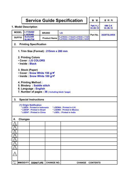
1.<br />
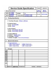
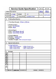
Model Description<br />
MODEL L173SAB/<br />
L193SAB<br />
BRAND<br />
SUFFIX SLEUAW<br />
SLWUTW<br />
Product Name<br />
2.<br />
3.<br />
4.<br />
8<br />
7<br />
6<br />
5<br />
4<br />
3<br />
2<br />
1<br />
REV.<br />
NO.<br />
Service Guide Specification<br />
Printing Specification<br />
1. Trim Size (Format) : 215mm x 280 mm<br />
2. Printing Colors<br />
Cover : LG COLORS<br />
Inside : Black<br />
3. Stock (Paper)<br />
Cover : Snow White 150 g/����<br />
Inside : Snow White 100 g/����<br />
4. Printing Method :<br />
5. Bindery : Saddle stitch<br />
6. Language : English<br />
7. Number of pages : 36 ( Including blank 1page)<br />
Special Inst<strong>ru</strong>ctions<br />
Changes<br />
���� ���� ���� ���� ����<br />
�������� �������� �������� ��������<br />
�������� �������� �������� ��������<br />
Part No.<br />
MM/DD/YY ���������<br />
���������<br />
���������<br />
��������� CHANGE NO. CHANGE CONTENTS<br />
LG<br />
FLATRON L173SA/FLATRON L173ST<br />
FLATRON L193SA/FLATRON L193ST<br />
(1) Origin Notification<br />
* LGEDI : Printed in Indonesia * LGEWA : Printed in U.K.<br />
* LGESP : Printed in Brazil * LGEMX : Printed in Mexico<br />
* LGENT : Printed in China * LGEIL : Printed in India<br />
������� ������� ������� �������<br />
�������� �������� �������� ��������<br />
3828TSL095X
Cover<br />
Front<br />
Cover<br />
inside<br />
Blank<br />
English<br />
29<br />
English<br />
2<br />
English<br />
30<br />
Pagination sheet<br />
English<br />
3<br />
English<br />
31<br />
English<br />
4<br />
English<br />
32<br />
English<br />
….<br />
English<br />
33<br />
English<br />
…..<br />
Rear<br />
Cover<br />
Inside<br />
34<br />
Rear<br />
Cover<br />
����� ����������������<br />
����� �����<br />
�������������<br />
������������� �������������<br />
������������� �������
Website:http://biz.LGservice.com<br />
E-mail:http://www.LGEservice.com/techsup.html<br />
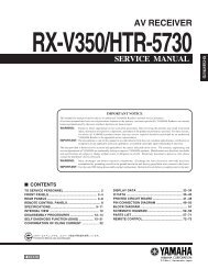
COLOR MONITOR<br />
SERVICE MANUAL<br />
CHASSIS NO. : CL-77<br />
MODEL: L193SA (L193SAB-AL**A)<br />
L193ST (L193SAB-AL**T)<br />
L173SA (L173SAB-AL**A)<br />
L173ST (L173SAB-AL**T)<br />
( ) **Same model for Service<br />
CAUTION<br />
BEFORE SERVICING THE UNIT,<br />
READ THE SAFETY PRECAUTIONS IN THIS MANUAL.
- 1 -
SPECIFICATIONS ................................................... 2<br />
PRECAUTIONS ....................................................... 3<br />
SERVICE PRECAUTIONS ...................................... 5<br />
TIMING CHART ....................................................... 8<br />
BLOCK DIAGRAM ................................................... 9<br />
DESCRIPTION OF BLOCK DIAGRAM ................. 10<br />
1. LCD CHARACTERISTICS<br />
Type : TFT Color LCD Module<br />
Size : 296.5(H) x 358.5(V) x 17.0(D)-L173SAB<br />
: 330.0(H) x 404.2(V) x 20.0(D)-L193SAB<br />
Pixel Pitch : 0.264mm x 0.264mm -L173SAB<br />
: 0.294mm x 0.294mm -L193SAB<br />
Color Depth : 6bits(with FRC)/ 16.2M colors<br />
Active Video Area : 17inch (432.7mm) -L173SAB<br />
: 19inch (481.84mm) -L193SAB<br />
Surface Treatment : Anti-Glare, Hard Coating (3H)<br />
Backlight Unit : 4CCFL<br />
Opraating Mode : Transmissive mode, Normally white<br />
Electrical Interface : LVDS interface<br />
2. OPTICAL CHARACTERISTICS<br />
2-1. Viewing Angle by Contrast Ratio ≥ 10<br />
Right : +60° min. +70° typ. Left : -60° min. -70° typ.<br />
Top : +60° min. +70° typ. Bottom: -60° min. -70° typ.<br />
2-2. Luminance<br />
: 320(min.), 400(typ.)<br />
2-3. Contrast Ratio : 300(min.), 500(typ.)<br />
3. SIGNAL (Refer to the Timing Chart)<br />
3-1. Sync Signal<br />
1) Type : Separate Sync, Composite, SOG, Digital<br />
3-3. Operating Frequency<br />
Horizontal(Analog) : 30 ~ 83kHz<br />
(Digital) : 30 ~ 71kHz<br />
Vertical : 56 ~ 75Hz<br />
4. SPECIAL FUNCTION<br />
4-1. Audio AMP<br />
1) Output: 3Wrms + 3Wrms<br />
2) Freq. Character: 100Hz~10KHz Range(-3dB)<br />
3) Input: PC - 0.7±0.1Vrms<br />
AV - 0.5±0.1Vrms<br />
4-2. SPEAKER<br />
1) Impedance : 16Ω<br />
2) Input : Max-4.5W, Normal-3W<br />
CONTENTS<br />
SPECIFICATIONS<br />
- 2 -<br />
ADJUSTMENT ...................................................... 12<br />
TROUBLESHOOTING GUIDE .............................. 14<br />
WIRING DIAGRAM ............................................... 18<br />
EXPLODED VIEW...................................................19<br />
REPLACEMENT PARTS LIST ...............................21<br />
SCHEMATIC DIAGRAM......................................... 27<br />
4-3. TV<br />
1) Type : PAL/SECAM<br />
2) Tuner IF : PIF - 38.9MHz<br />
SIF - 33.4MHz<br />
CIF - 34.47MHz<br />
3) Receiving Channel : VHF- Low: 45.25~140.25MHz<br />
HIGH: 147.25~423.25MHz<br />
UHF - 431.25~855.25MHz<br />
4-4. AV<br />
1) Video Level : Input - 0.7±0.15Vp-p<br />
2) Sync Level : Input - 0.286±0.075Vp-p<br />
3) Color Burst : Input - 0.214±0.072Vp-p<br />
4) Audio Level : AV Input - 0.5±0.1Vrms<br />
PC Input - 0.7±0.1Vrms<br />
5) Video Cross Talk : 43dB<br />
5. Max Resolution<br />
SXGA(Analog) : 1280 x 1024@75Hz<br />
SXGA(Digital) : 1280 x 1024@60Hz<br />
6. POWER SUPPLY<br />
6-1. Power<br />
100-240V~, 50/60Hz<br />
6-2. Power Consumption<br />
MODE<br />
POWER ON (NORMAL)<br />
STAND-BY<br />
SUSPEND<br />
POWER OFF<br />
AUDIO OUTPUT<br />
7. ENVIRONMENT<br />
H/V SYNC<br />
ON/ON<br />
OFF/ON<br />
ON/OFF<br />
OFF<br />
Source<br />
PC<br />
AV<br />
TV<br />
AV<br />
VIDEO<br />
ACTIVE<br />
OFF<br />
OFF<br />
OFF<br />
Min<br />
2.7W<br />
1.4W<br />
2.7W<br />
2.7W<br />
POWER CONSUMPTION<br />
less than 55 W<br />
less than 3 W<br />
less than 3 W<br />
less than 3 W<br />
7-1. Operating Temperature: 10°C~35°C (50°F~95°F)<br />
7-2. Operating Humidity : 20%~80%<br />
7-3. MTBF : 50,000 Hours (Min.)<br />
Typ<br />
3W<br />
1.6W<br />
3W<br />
3W<br />
Max<br />
4W<br />
2.5W<br />
4W<br />
4W<br />
LED COLOR<br />
BLUE<br />
AMBER<br />
AMBER<br />
AMBER<br />
L173ST/L193ST<br />
L173ST/L193ST<br />
L173SA/L193SA
8. DIMENSIONS(WxLxH) 9. WEIGHT (with TILT)<br />
10.General Specification(TV)<br />
1<br />
2<br />
3<br />
No.<br />
Video input applicable system<br />
Receivable broadcasting system<br />
RF input channel<br />
474.5mm x 242.0 mm x 401.7mm(L173SAB)<br />
517.0mm x 242.0mm x 436.0mm(L193SAB)<br />
474.5mm x 115.2 mm x 447.7mm(L173SAB)<br />
517.0mm x 119.2mm x 481.7mm(L193SAB)<br />
Item Specification Remark<br />
1)PAL-D/K,B/G,I, SECAM<br />
1)PAL/SECAM BG<br />
2)PAL/SECAM DK<br />
3)PAL I/I<br />
4)SECAM L/L'<br />
VHF : E2 ~ E12<br />
UHF : E21 ~ E69<br />
CATV : S1 ~ S20<br />
HYPER : S21 ~ S41<br />
L/L’ : B,C,D<br />
Net. Weight : 6.84kg (15.0 lbs)-L173SAB<br />
: 7.96kg (17.5 lbs)-L193SAB<br />
Gross Weight : 10.5kg (23.15 lbs)-L173SAB<br />
: 11.5kg (25.35 lbs)-L193SAB<br />
EU Market<br />
PAL<br />
FRANCE
WARNING FOR THE SAFETY-RELATED COMPONENT.<br />
• There are some special components used in LCD<br />
monitor that are important for safety. These parts are<br />
marked on the schematic diagram and the<br />
replacement parts list. It is essential that these critical<br />
parts should be replaced with the manufacturer’s<br />
specified parts to prevent electric shock, fire or other<br />
hazard.<br />
• Do not modify original design without obtaining written<br />
permission from manufacturer or you will void the<br />
original parts and labor guarantee.<br />
TAKE CARE DURING HANDLING THE LCD MODULE<br />
WITH BACKLIGHT UNIT.<br />
• Must mount the module using mounting holes arranged<br />
in four corners.<br />
• Do not press on the panel, edge of the frame strongly<br />
or electric shock as this will result in damage to the<br />
screen.<br />
• Do not scratch or press on the panel with any sharp<br />
objects, such as pencil or pen as this may result in<br />
damage to the panel.<br />
• Protect the module from the ESD as it may damage the<br />
electronic circuit (C-MOS).<br />
• Make certain that treatment person’s body are<br />
grounded through wrist band.<br />
• Do not leave the module in high temperature and in<br />
areas of high humidity for a long time.<br />
• The module not be exposed to the direct sunlight.<br />
• Avoid contact with water as it may a short circuit within<br />
the module.<br />
• If the surface of panel become dirty, please wipe it off<br />
with a softmaterial. (Cleaning with a dirty or rough cloth<br />
may damage the panel.)<br />
CAUTION<br />
Please use only a plastic screwdriver to protect yourself<br />
from shock hazard during service operation.<br />
PRECAUTION<br />
- 4 -<br />
WARNING<br />
BE CAREFUL ELECTRIC SHOCK !<br />
• If you want to replace with the new backlight (CCFL) or<br />
inverter circuit, must disconnect the AC adapter<br />
because high voltage appears at inverter circuit about<br />
650Vrms.<br />
• Handle with care wires or connectors of the inverter<br />
circuit. If the wires are pressed cause short and may<br />
burn or take fire.<br />
Leakage Current Hot Check Circuit<br />
To Inst<strong>ru</strong>ment's<br />
exposed<br />
METALLIC PARTS<br />
AC Volt-meter<br />
1.5 Kohm/10W<br />
Good Earth Ground<br />
such as WATER PIPE,<br />
CONDUIT etc.
CAUTION: Before servicing receivers covered by this<br />
service manual and its supplements and addenda, read<br />
and follow the SAFETY PRECAUTIONS on page 3 of this<br />
publication.<br />
NOTE: If unforeseen circumstances create conflict<br />
between the following servicing precautions and any of the<br />
safety precautions on page 3 of this publication, always<br />
follow the safety precautions. Remember: Safety First.<br />
General Servicing Precautions<br />
1. Always unplug the receiver AC power cord from the AC<br />
power source before;<br />
a. Removing or reinstalling any component, circuit<br />
board module or any other receiver assembly.<br />
b. Disconnecting or reconnecting any receiver electrical<br />
plug or other electrical connection.<br />
c. Connecting a test substitute in parallel with an<br />
electrolytic capacitor in the receiver.<br />
CAUTION: A wrong part substitution or incorrect<br />
polarity installation of electrolytic capacitors may<br />
result in an explosion hazard.<br />
d. Discharging the picture tube anode.<br />
2. Test high voltage only by measuring it with an<br />
appropriate high voltage meter or other voltage<br />
measuring device (DVM, FETVOM, etc) equipped with<br />
a suitable high voltage probe.<br />
Do not test high voltage by "drawing an arc".<br />
3. Discharge the picture tube anode only by (a) first<br />
connecting one end of an insulated clip lead to the<br />
degaussing or kine aquadag grounding system shield<br />
at the point where the picture tube socket ground lead<br />
is connected, and then (b) touch the other end of the<br />
insulated clip lead to the picture tube anode button,<br />
using an insulating handle to avoid personal contact<br />
with high voltage.<br />
4. Do not spray chemicals on or near this receiver or any<br />
of its assemblies.<br />
5. Unless specified otherwise in this service manual,<br />
clean electrical contacts only by applying the following<br />
mixture to the contacts with a pipe cleaner, cottontipped<br />
stick or comparable non-abrasive applicator;<br />
10% (by volume) Acetone and 90% (by volume)<br />
isopropyl alcohol (90%-99% strength)<br />
CAUTION: This is a flammable mixture.<br />
Unless specified otherwise in this service manual,<br />
lubrication of contacts in not required.<br />
6. Do not defeat any plug/socket B+ voltage interlocks<br />
with which receivers covered by this service manual<br />
might be equipped.<br />
7. Do not apply AC power to this inst<strong>ru</strong>ment and/or any of<br />
its electrical assemblies unless all solid-state device<br />
heat sinks are correctly installed.<br />
8. Always connect the test receiver ground lead to the<br />
receiver chassis ground before connecting the test<br />
receiver positive lead.<br />
Always remove the test receiver ground lead last.<br />
SERVICING PRECAUTIONS<br />
- 5 -<br />
9. Use with this receiver only the test fixtures specified in<br />
this service manual.<br />
CAUTION: Do not connect the test fixture ground strap<br />
to any heat sink in this receiver.<br />
Electrostatically Sensitive (ES) Devices<br />
Some semiconductor (solid-state) devices can be<br />
damaged easily by static electricity. Such components<br />
commonly are called Electrostatically Sensitive (ES)<br />
Devices. Examples of typical ES devices are integrated<br />
circuits and some field-effect transistors and<br />
semiconductor "chip" components. The following<br />
techniques should be used to help reduce the incidence of<br />
component damage caused by static by static electricity.<br />
1. Immediately before handling any semiconductor<br />
component or semiconductor-equipped assembly, drain<br />
off any electrostatic charge on your body by touching a<br />
known earth ground. Alternatively, obtain and wear a<br />
commercially available discharging wrist strap device,<br />
which should be removed to prevent potential shock<br />
reasons prior to applying power to the unit under test.<br />
2. After removing an electrical assembly equipped with<br />
ES devices, place the assembly on a conductive<br />
surface such as aluminum foil, to prevent electrostatic<br />
charge buildup or exposure of the assembly.<br />
3. Use only a grounded-tip soldering iron to solder or<br />
unsolder ES devices.<br />
4. Use only an anti-static type solder removal device.<br />
Some solder removal devices not classified as "antistatic"<br />
can generate electrical charges sufficient to<br />
damage ES devices.<br />
5. Do not use freon-propelled chemicals. These can<br />
generate electrical charges sufficient to damage ES<br />
devices.<br />
6. Do not remove a replacement ES device from its<br />
protective package until immediately before you are<br />
ready to install it. (Most replacement ES devices are<br />
packaged with leads electrically shorted together by<br />
conductive foam, aluminum foil or comparable<br />
conductive material).<br />
7. Immediately before removing the protective material<br />
from the leads of a replacement ES device, touch the<br />
protective material to the chassis or circuit assembly<br />
into which the device will be installed.<br />
CAUTION: Be sure no power is applied to the chassis<br />
or circuit, and observe all other safety precautions.<br />
8. Minimize bodily motions when handling unpackaged<br />
replacement ES devices. (Otherwise harmless motion<br />
such as the b<strong>ru</strong>shing together of your clothes fabric or<br />
the lifting of your foot from a carpeted floor can<br />
generate static electricity sufficient to damage an ES<br />
device.)
General Soldering Guidelines<br />
1. Use a grounded-tip, low-wattage soldering iron and<br />
appropriate tip size and shape that will maintain tip<br />
temperature within the range or 500。F to 600。F.<br />
2. Use an appropriate gauge of RMA resin-core solder<br />
composed of 60 parts tin/40 parts lead.<br />
3. Keep the soldering iron tip clean and well tinned.<br />
4. Thoroughly clean the surfaces to be soldered. Use a<br />
mall wire-bristle (0.5 inch, or 1.25cm) b<strong>ru</strong>sh with a<br />
metal handle.<br />
Do not use freon-propelled spray-on cleaners.<br />
5. Use the following unsoldering technique<br />
a. Allow the soldering iron tip to reach normal<br />
temperature.<br />
(500。F to 600。F)<br />
b. Heat the component lead until the solder melts.<br />
c. Quickly draw the melted solder with an anti-static,<br />
suction-type solder removal device or with solder<br />
braid.<br />
CAUTION: Work quickly to avoid overheating the<br />
circuitboard printed foil.<br />
6. Use the following soldering technique.<br />
a. Allow the soldering iron tip to reach a normal<br />
temperature (500。F to 600。F)<br />
b. First, hold the soldering iron tip and solder the strand<br />
against the component lead until the solder melts.<br />
c. Quickly move the soldering iron tip to the junction of<br />
the component lead and the printed circuit foil, and<br />
hold it there only until the solder flows onto and<br />
around both the component lead and the foil.<br />
CAUTION: Work quickly to avoid overheating the<br />
circuit board printed foil.<br />
d. Closely inspect the solder area and remove any<br />
excess or splashed solder with a small wire-bristle<br />
b<strong>ru</strong>sh.<br />
IC Remove/Replacement<br />
Some chassis circuit boards have slotted holes (oblong)<br />
through which the IC leads are inserted and then bent flat<br />
against the circuit foil. When holes are the slotted type,<br />
the following technique should be used to remove and<br />
replace the IC. When working with boards using the<br />
familiar round hole, use the standard technique as<br />
outlined in paragraphs 5 and 6 above.<br />
Removal<br />
1. Desolder and straighten each IC lead in one operation<br />
by gently prying up on the lead with the soldering iron<br />
tip as the solder melts.<br />
2. Draw away the melted solder with an anti-static<br />
suction-type solder removal device (or with solder<br />
braid) before removing the IC.<br />
- 6 -<br />
Replacement<br />
1. Carefully insert the replacement IC in the circuit board.<br />
2. Carefully bend each IC lead against the circuit foil pad<br />
and solder it.<br />
3. Clean the soldered areas with a small wire-bristle<br />
b<strong>ru</strong>sh. (It is not necessary to reapply acrylic coating to<br />
the areas).<br />
"Small-Signal" Discrete Transistor<br />
Removal/Replacement<br />
1. Remove the defective transistor by clipping its leads as<br />
close as possible to the component body.<br />
2. Bend into a "U" shape the end of each of three leads<br />
remaining on the circuit board.<br />
3. Bend into a "U" shape the replacement transistor leads.<br />
4. Connect the replacement transistor leads to the<br />
corresponding leads extending from the circuit board<br />
and crimp the "U" with long nose pliers to insure metal<br />
to metal contact then solder each connection.<br />
Power Output, Transistor Device<br />
Removal/Replacement<br />
1. Heat and remove all solder from around the transistor<br />
leads.<br />
2. Remove the heat sink mounting screw (if so equipped).<br />
3. Carefully remove the transistor from the heat sink of the<br />
circuit board.<br />
4. Insert new transistor in the circuit board.<br />
5. Solder each transistor lead, and clip off excess lead.<br />
6. Replace heat sink.<br />
Diode Removal/Replacement<br />
1. Remove defective diode by clipping its leads as close<br />
as possible to diode body.<br />
2. Bend the two remaining leads perpendicular y to the<br />
circuit board.<br />
3. Observing diode polarity, wrap each lead of the new<br />
diode around the corresponding lead on the circuit<br />
board.<br />
4. Securely crimp each connection and solder it.<br />
5. Inspect (on the circuit board copper side) the solder<br />
joints of the two "original" leads. If they are not shiny,<br />
reheat them and if necessary, apply additional solder.<br />
Fuse and Conventional Resistor<br />
Removal/Replacement<br />
1. Clip each fuse or resistor lead at top of the circuit board<br />
hollow stake.<br />
2. Securely crimp the leads of replacement component<br />
around notch at stake top.<br />
3. Solder the connections.<br />
CAUTION: Maintain original spacing between the<br />
replaced component and adjacent components and the<br />
circuit board to prevent excessive component<br />
temperatures.
Circuit Board Foil Repair<br />
Excessive heat applied to the copper foil of any printed<br />
circuit board will weaken the adhesive that bonds the foil<br />
to the circuit board causing the foil to separate from or<br />
"lift-off" the board. The following guidelines and<br />
procedures should be followed whenever this condition is<br />
encountered.<br />
At IC Connections<br />
To repair a defective copper pattern at IC connections use<br />
the following procedure to install a jumper wire on the<br />
copper pattern side of the circuit board. (Use this<br />
technique only on IC connections).<br />
1. Carefully remove the damaged copper pattern with a<br />
sharp knife. (Remove only as much copper as<br />
absolutely necessary).<br />
2. carefully scratch away the solder resist and acrylic<br />
coating (if used) from the end of the remaining copper<br />
pattern.<br />
3. Bend a small "U" in one end of a small gauge jumper<br />
wire and carefully crimp it around the IC pin. Solder the<br />
IC connection.<br />
4. Route the jumper wire along the path of the out-away<br />
copper pattern and let it overlap the previously scraped<br />
end of the good copper pattern. Solder the overlapped<br />
area and clip off any excess jumper wire.<br />
- 7 -<br />
At Other Connections<br />
Use the following technique to repair the defective copper<br />
pattern at connections other than IC Pins. This technique<br />
involves the installation of a jumper wire on the<br />
component side of the circuit board.<br />
1. Remove the defective copper pattern with a sharp<br />
knife.<br />
Remove at least 1/4 inch of copper, to ensure that a<br />
hazardous condition will not exist if the jumper wire<br />
opens.<br />
2. Trace along the copper pattern from both sides of the<br />
pattern break and locate the nearest component that is<br />
directly connected to the affected copper pattern.<br />
3. Connect insulated 20-gauge jumper wire from the lead<br />
of the nearest component on one side of the pattern<br />
break to the lead of the nearest component on the<br />
other side.<br />
Carefully crimp and solder the connections.<br />
CAUTION: Be sure the insulated jumper wire is<br />
dressed so the it does not touch components or sharp<br />
edges.
MODE<br />
1<br />
2<br />
3<br />
4<br />
5<br />
6<br />
7<br />
8<br />
9<br />
10<br />
11<br />
12<br />
13<br />
H / V<br />
H (Pixels)<br />
V (Lines)<br />
H (Pixels)<br />
V (Lines)<br />
H (Pixels)<br />
V (Lines)<br />
H (Pixels)<br />
V (Lines)<br />
H (Pixels)<br />
V (Lines)<br />
H (Pixels)<br />
V (Lines)<br />
H (Pixels)<br />
V (Lines)<br />
H (Pixels)<br />
V (Lines)<br />
H (Pixels)<br />
V (Lines)<br />
H (Pixels)<br />
V (Lines)<br />
H (Pixels)<br />
V (Lines)<br />
H (Pixels)<br />
V (Lines)<br />
H (Pixels)<br />
V (Lines)<br />
VIDEO<br />
SYNC<br />
Sync<br />
Polarity<br />
+<br />
–<br />
–<br />
+<br />
–<br />
–<br />
–<br />
–<br />
+<br />
+<br />
+<br />
+<br />
+/–<br />
+/–<br />
–<br />
–<br />
–<br />
–<br />
+/–<br />
+/–<br />
+/–<br />
+/–<br />
+<br />
+<br />
+<br />
+<br />
Dot<br />
Clock<br />
25.175<br />
28.321<br />
25.175<br />
31.5<br />
40.0<br />
49.5<br />
57.283<br />
65.0<br />
78.75<br />
100.0<br />
92.978<br />
108.0<br />
135.0<br />
D<br />
C<br />
Frequency<br />
31.469 KHz<br />
70.09 Hz<br />
31.468 KHz<br />
70.08 Hz<br />
31.469 KHz<br />
59.94 Hz<br />
37.5 KHz<br />
75 Hz<br />
37.879 KHz<br />
60.317 Hz<br />
46.875 KHz<br />
75.0 Hz<br />
49.725KHz<br />
74.55 Hz<br />
48.363 KHz<br />
60.0 Hz<br />
60.123KHz<br />
75.029 Hz<br />
68.681 KHz<br />
75.062 Hz<br />
61.805 KHz<br />
65.96 Hz<br />
63.981 KHz<br />
60.02 Hz<br />
79.976KHz<br />
75.035 Hz<br />
TIMING CHART<br />
Total<br />
Period<br />
( E )<br />
800<br />
449<br />
900<br />
449<br />
800<br />
525<br />
840<br />
500<br />
1056<br />
628<br />
1056<br />
625<br />
1152<br />
667<br />
1344<br />
806<br />
1312<br />
800<br />
1456<br />
915<br />
1504<br />
937<br />
1688<br />
1066<br />
1688<br />
1066<br />
B<br />
- 8 -<br />
E<br />
A<br />
Video<br />
Active<br />
Time ( A )<br />
640<br />
350<br />
720<br />
400<br />
640<br />
480<br />
640<br />
480<br />
800<br />
600<br />
800<br />
600<br />
832<br />
624<br />
1024<br />
768<br />
1024<br />
768<br />
1152<br />
870<br />
1152<br />
900<br />
1280<br />
1024<br />
1280<br />
1024<br />
Blanking<br />
Time<br />
( B )<br />
16<br />
37<br />
18<br />
12<br />
16<br />
10<br />
16<br />
1<br />
40<br />
1<br />
16<br />
1<br />
32<br />
1<br />
24<br />
3<br />
16<br />
1<br />
32<br />
3<br />
18<br />
2<br />
48<br />
1<br />
16<br />
1<br />
Sync<br />
Duration<br />
( D )<br />
96<br />
2<br />
108<br />
2<br />
96<br />
2<br />
64<br />
3<br />
128<br />
4<br />
80<br />
3<br />
64<br />
3<br />
136<br />
6<br />
96<br />
3<br />
128<br />
3<br />
134<br />
4<br />
112<br />
3<br />
144<br />
3<br />
Back<br />
Porch<br />
( F )<br />
48<br />
60<br />
55<br />
35<br />
48<br />
33<br />
120<br />
16<br />
88<br />
23<br />
160<br />
21<br />
224<br />
39<br />
160<br />
29<br />
176<br />
28<br />
144<br />
39<br />
200<br />
31<br />
248<br />
38<br />
248<br />
38<br />
Resolution<br />
640 x 350<br />
720 x 400<br />
640 x 480<br />
640 x 480<br />
800 x 600<br />
800 x 600<br />
832 x 624<br />
1024 x 768<br />
1024 x 768<br />
1152 x 870<br />
1152 x 900<br />
1280 x 1024<br />
1280 x 1024
SP (R) SP (L)<br />
LCD Module<br />
Key<br />
H/p hone<br />
(TPA6110)<br />
Audio-R<br />
Aud io<br />
amp<br />
(TPA300 4)<br />
LVDS<br />
Audio-L<br />
AUDIO<br />
CVBS<br />
YUV 8bit ,Clock,IIC,<br />
PC Audi o,POWER,<br />
CVBS,S VIDEO,AUDIO<br />
SVID EO<br />
BLOCK DIAGRAM<br />
AUDIO<br />
YUV 8bit ,Clock<br />
15V<br />
5V<br />
INV on<br />
BRT ADJ<br />
MIC<br />
IIC<br />
POWER<br />
AD C<br />
MST9 883C<br />
YUV 8bit<br />
Clock<br />
INV_ONOFF<br />
BRI_ADJ<br />
DC/DC<br />
Block<br />
IIC RGB,HS,VS<br />
IIC<br />
- 9 -<br />
IIC<br />
Mic om<br />
MTV412<br />
LIPS<br />
SAW<br />
VCT49xy<br />
(A/V DE C)<br />
8bit<br />
IF<br />
CVBS<br />
CVB S<br />
Video Signal<br />
Process or<br />
(MST51510)<br />
W/W<br />
Tuner<br />
Audio<br />
L/R<br />
Audio<br />
L/R<br />
RGB<br />
PC<br />
Audio<br />
S<br />
D<br />
R<br />
A<br />
M<br />
Analog<br />
Digital<br />
SCART<br />
DVI-D DSUB<br />
MIC
DESCRIPTION OF BLOCK DIAGRAM<br />
1. Format Converter (MST9883C)(U702)<br />
This IC contain A/D converter, Pre-amp and PLL circuit that converting<br />
Analog video signal(0.7p-p RGB) to digital signal.(656 Format)<br />
2. Power Supply Block (LIPS)<br />
This Block Generates DC Voltage (5V,15V) to Main Control system from AC Power (100-240 V, 50/60 Hz, 1.0A)<br />
The Minimum of Power efficiency is about 80%.<br />
3. DC/DC Converter block<br />
DC/DC Converter convert the input 5V,15V to proper 3.3V,5V,12V for<br />
Main control system.<br />
For shooting heat trouble, we use the DC/DC converting IC<br />
4. Audio Amplifier (TPA3004D2)(U201)<br />
This block is composed of TPA3004D2 and peripheral device<br />
The function of the audio amplifier is that to amplify audio L / R signal transmitted from audio decoder. The audio signal is amplified<br />
according to pre-defined DC volume control curve. Also, headphone amplifier (TPA6110) is controlled through line-out<br />
5. Audio / Video / IF Decoder(U601)<br />
This block is composed of VCT49xy and peripheral devices.<br />
Micom controls this IC through IIC Line.<br />
1) Video Decoder<br />
This Block Selects input Video signals (like CVBS, Y/C, SCART RGB) and output RGB signal.<br />
On decoding, We can control signal like Contrast, Brightness, Sharpness, Color, tint signals including Adaptive Comb Filter<br />
2) Audio Decoder<br />
This block analyzes audio input signal through A/V Jack and PC audio and Tuner IF.<br />
The analyzed signals transmitted to audio amplifier (TPA3004D2)<br />
On decoding, We can control signal like Bass, treble.<br />
3) IF Decoder<br />
This block can change IF signal to audio and video signal that transmitted to Video/audio decoder.<br />
6. Video signal processor (Scaler IC)(U401)<br />
It is composed of MST51510<br />
Micom controls this IC through IIC Line.<br />
This IC includes A/D Converter and LVDS Transmitter<br />
This IC is directly Inputted Analog and Digital Signal and transmits to LCD Module<br />
7. MICOM(U501)<br />
It is composed of MTV412<br />
This IC controls peripheral devices through IIC line<br />
8. TUNER(TU802)<br />
Micom controls this IC through IIC Line.<br />
TUNER makes IF and transmits IF signal to VCT49xy.<br />
- 10 -
50 ~ 60Hz<br />
LINE<br />
100 ~ 240V<br />
EMI<br />
COMPONENTS<br />
LIPS Board Block Diagram<br />
INPUT RECTIFIER<br />
AND FILTER<br />
PWM<br />
CONTROL<br />
CIRCUIT<br />
HVDC<br />
- 11 -<br />
ENERGY<br />
TRANSFER<br />
PHOTO-<br />
COUPLER<br />
ISOLATION<br />
100KHz<br />
OUTPUT RECTIFIER<br />
AND FILTER<br />
SIGNAL<br />
COLLECTI<br />
ON<br />
PRIMARY SECONDARY<br />
Operation description_LIPS<br />
1. EMI components.<br />
This part contains of EMI components to comply with global marketing EMI standards like FCC,VCCI CISPR,<br />
the circuit included a line-filter, across line capacitor and of course the primary protection fuse.<br />
2. Input rectifier and filter.<br />
This part function is for transfer the input AC voltage to a DC voltage through a bridge rectifier and a bulk capacitor.<br />
3. Energy Transfer.<br />
This part function is for transfer the primary energy to secondary through a power transformer.<br />
4. Output rectifier and filter.<br />
This part function is to make a pulse width modulation control and to provide the driver signal to power switch,to<br />
adjust the duty cycle during different AC input and output loading condition to achieve the dc output stabilized, and<br />
also the over power protection is also monitor by this part.<br />
5. Photo-Coupler isolation.<br />
This part function is to feed back the dc output changing status through a photo transistor to primary controller to<br />
achieve the stabilized dc output voltage.<br />
6. Signal collection.<br />
This part function is to collect the any change from the dc output and feed back to the primary through photo<br />
transistor<br />
12V<br />
5V<br />
GND
Windows EDID V1.0 User Manual<br />
Operating System: MS Windows 98, 2000, XP<br />
Port Setup: Windows 98 => Don’t need setup<br />
Windows 2000, XP => Need to Port Setup.<br />
This program is available to LCD Monitor only.<br />
1. Port Setup<br />
a) Copy “UserPort.sys” file to<br />
“c:\WINNT\system32\drivers” folder<br />
b) Run Userport.exe<br />
c) Remove all default number<br />
d) Add 300-3FF<br />
e) Click Start button.<br />
f) Click Exit button.<br />
ADJUSTMENT<br />
- 12 -<br />
2. EDID Read & Write<br />
1) Run WinEDID.exe<br />
2) Edit Week of Manufacture, Year of Manufacture,<br />
Serial Number<br />
a) Input User Info Data<br />
b) Click “Update” button<br />
c) Click “ Write” button<br />
EEPROM initialize:<br />
ADC adjustment : <br />
Aging off: <br />
Module selection :
Video Signal<br />
Generator<br />
Control Line<br />
Audio In<br />
MIC.Out<br />
C<br />
S-Video<br />
MIC.In<br />
A<br />
Not used<br />
PARALLEL<br />
RS232C<br />
VGS MONITOR<br />
B<br />
V-SYNC ST POWER<br />
F<br />
IBM<br />
Compatible PC<br />
E<br />
220<br />
Power inlet (required)<br />
Power Select Switch<br />
(110V/220V)<br />
Power LED<br />
ST Switch<br />
V-Sync On/Off Switch<br />
(Switch must be ON.)<br />
Figure 1. Cable Connection<br />
- 13 -<br />
PARALLEL PORT<br />
5V<br />
F<br />
15<br />
10<br />
5<br />
OFF ON<br />
A<br />
B<br />
11<br />
6<br />
1<br />
5<br />
9<br />
ON<br />
OFF<br />
E<br />
6<br />
1<br />
13<br />
25<br />
5V<br />
74LS06<br />
4.7K<br />
C<br />
5V<br />
4.7K<br />
4.7K<br />
74LS06<br />
1<br />
14
1<br />
1<br />
2<br />
3<br />
Waveforms<br />
NO POWER<br />
(POWER INDICATOR OFF)<br />
CHECK J103 VOLTAGE<br />
PIN5, PIN6 (5V)?<br />
YES<br />
CHECK<br />
U501 PIN 8 Voltage<br />
(5V) ?<br />
YES<br />
CHECK KEY CONTROL<br />
CONNECTOR ROUTINE<br />
YES<br />
IS U401<br />
PIN55 (3.3V)<br />
VOLTAGE ?<br />
YES<br />
CHECK U401 PIN 171<br />
PULSE<br />
YES<br />
CHECK U401<br />
TROUBLESHOOTING GUIDE<br />
1. NO POWER<br />
:[A]PROCESS<br />
1 J103-#5, 6 / U501-#8 2 U401-#55 3 U401-#177<br />
NO<br />
NO<br />
NO<br />
NO<br />
- 14 -<br />
CHECK LIPS, AND FIND OUT A<br />
SHORT POINT<br />
AS OPENING<br />
EACH POWER LINE<br />
CHECK 5VS LINE<br />
(OPEN CHECK)<br />
CHECK 3.3V LINE<br />
CHECK X-TAL(X501)<br />
NO PROBLEM
4<br />
5<br />
6<br />
NO RASTER<br />
ON AV SIGNAL<br />
REPEAT [A]: PROCESS<br />
PASS<br />
CHACK INPUT SOURCE<br />
CABLE AND JACK<br />
PASS<br />
CHECK J108<br />
PASS<br />
CHECK<br />
ZD 814, ZD815<br />
OPEN TEST<br />
CHECK<br />
U901(1.8V)?<br />
PASS(Open)<br />
PASS<br />
CHECK<br />
U902(3.3V)?<br />
PASS<br />
CHECK<br />
U601 PIN101<br />
PASS<br />
CHECK<br />
U702 THE INPUT/OUTPUT<br />
OF U702<br />
PASS<br />
CHACK THHE INPUT/OUTPUT<br />
OF BA702, BA704<br />
2. NO RASTER(AV SIGNAL)<br />
NO SIGNAL<br />
FAIL(Shore)<br />
FAIL<br />
FAIL<br />
Waveforms<br />
4 U901 5 U902<br />
- 15 -<br />
CHECK SIDE AV<br />
CONNECTOR<br />
RANTINE<br />
CHANGE ZD814, ZD815<br />
CHECK 1.8V LINE<br />
CHECK 3.3V LINE<br />
FAIL RE-SOLDERING OR<br />
CHECK X-TAL(X601)<br />
FAIL RE-SOLDERING OR<br />
CHANGE THE DEFECT PART<br />
6 U601-#101<br />
:[B]PROCESS
7<br />
J802-#11<br />
Waveforms<br />
NO RASTER ON<br />
TV(RF) SIGNAL<br />
REPEAT [A]PROCESS<br />
PASS<br />
CHECK ANTENNA CABLE<br />
PASS<br />
CHECKU904(8V)?<br />
PASS<br />
CHECKU903(5V)?<br />
PASS<br />
CHECK TU802 PIN9(33V)?<br />
PASS<br />
REPEAT [B]:PROCESS<br />
3. NO RASTER(TV(RF) SIGNAL)<br />
FAIL<br />
FAIL<br />
- 16 -<br />
CHECK 33V STEP-UP CIRCUIT<br />
CHECK 8V LINE<br />
CHECK 5V LINE<br />
FAIL CHECK D903<br />
OPEN TEST<br />
FAIL<br />
7<br />
PASS<br />
CHECK J802 PIN11<br />
PASS<br />
PASS<br />
CHANGE D903<br />
FAIL CHECK U501<br />
MICOM
4<br />
6<br />
8<br />
4<br />
Waveforms<br />
NO SOUND<br />
CHECK<br />
THE INPUT SOURCE<br />
PASS<br />
CHECK U901(1.8V)?<br />
PASS<br />
CHECK U902(3.3V)?<br />
PASS<br />
CHECK U601 PIN101<br />
PASS<br />
CHECK U201 PIN 14, 15,<br />
22, 23, 38, 39, 46, 47)<br />
15V?<br />
PASS<br />
CHECK THE<br />
INPUT/OUTPUT OF<br />
U201<br />
PASS<br />
CHECK THE SPEAKER<br />
PASS<br />
CHECK THE SPEAKER LINE<br />
4. NO SOUND<br />
FAIL<br />
FAIL<br />
FAIL<br />
- 17 -<br />
CHANGE SOURCE INPUT<br />
CHECK 1.8V LINE<br />
CHECK 3.3V LINE<br />
FAIL RE-SOLDERING OR<br />
CHANGE THE DEFECT PART<br />
FAIL<br />
FAIL<br />
CHECK 15V LINE<br />
FAIL RE-SOLDERING OR<br />
CHANGE THE DEFECT PART<br />
CHANGE SPEAKER<br />
U901 6 U601-#101 8 U201-SPEAKER OUTPUT
8Pin<br />
CW401<br />
CW402<br />
CW404<br />
CW403<br />
Connector Ass’y P/N:<br />
6631T2006C<br />
Connector Ass’y P/N:<br />
6631T120029A<br />
WIRING DIAGRAM<br />
11Pin J110<br />
J103<br />
- 18 -<br />
30Pin<br />
J401<br />
Connector Ass’y P/N:<br />
6631T11012W<br />
J109 J108<br />
13Pin<br />
Connector Ass’y P/N:<br />
6631T20034B
EXPLODED VIEW<br />
105 101<br />
102<br />
101<br />
113<br />
106<br />
119<br />
115<br />
121<br />
114<br />
106<br />
107<br />
116<br />
108<br />
120<br />
109<br />
110<br />
- 19 -<br />
112<br />
111<br />
117<br />
118<br />
104<br />
124<br />
128<br />
122 123<br />
129<br />
130<br />
131 132<br />
125<br />
126<br />
127
Ref. No.<br />
101<br />
102<br />
103<br />
104<br />
105<br />
106<br />
107<br />
108<br />
109<br />
110<br />
111<br />
112<br />
113<br />
114<br />
115<br />
116<br />
117<br />
118<br />
119<br />
120<br />
121<br />
122<br />
123<br />
124<br />
125<br />
126<br />
127<br />
128<br />
129<br />
130<br />
131<br />
132<br />
EXPLODED VIEW PARTS LIST<br />
Part No.<br />
Description<br />
3091TKL110D CABINET ASSEMBLY, L173SAB BRAND 3090TKL098 MFM AV C-CKD(L173SA-For Europe)<br />
3091TKL110B CABINET ASSEMBLY, L173SAB BRAND 3090TKL098 MFM-CKD(L173ST-For West Europe)<br />
3091TKL111D CABINET ASSEMBLY, L193SAB BRAND 3090TKL099 MFM AV C-CKD(L193SA-For Europe)<br />
3091TKL111B CABINET ASSEMBLY, L193SAB BRAND 3090TKL099 MFM -CKD(L193ST-For West Europe)<br />
6304FLP152A LCD(LIQUID CRYSTAL DISPLAY), LM170E01-E5 LG PHILPS TFT COLOR 400NITS,TN,SXGA,LVDS(L173SA)<br />
6304FLP136A LCD(LIQUID CRYSTAL DISPLAY), LM190E03-A4 LG PHILPS TFT COLOR 20T,TN,400NITS,SXGA,LVDS(L193SA)<br />
3809TKL080D BACK COVER ASSEMBLY, L173SAB 3808TKL081 MFM C-CKD(L173SA-For Europe)<br />
3809TKL080B BACK COVER ASSEMBLY, L173SAB 3808TKL081 MFM-CKD (L173ST-For West Europe)<br />
3809TKL081D BACK COVER ASSEMBLY, L193SAB 3808TKL082 MFM C-CKD(L193SA-For Europe)<br />
3809TKL081B BACK COVER ASSEMBLY, L193SAB 3808TKL082 MFM-CKD(L193ST-For West Europe)<br />
3809TKL081C BACK COVER ASSEMBLY, L193SAB 3808TKL082 MFM PAL(L193SA-For Vietnam)<br />
3043TKK177B TILT SWIVEL ASSEMBLY, L173SAB/L193SAB 3550TKK573/574 MFM-CKD<br />
3043TKK177A TILT SWIVEL ASSEMBLY, L173SAB/L193SAB 3550TKK573/574 MFM-CKD(For Vietam)<br />
3550TKS092A COVER, L173SAL GRILL SPEAKER(MFM)(L173SA, L173ST)<br />
3550TKS093A COVER, L193SAL SPEAKER GRILL MFM(L193SA, L193ST)<br />
6401TZZ035D SPEAKER ASSEMBLY, L173/193SAB 3W,16OHM,4PIN, L500, L280,SHIELD"<br />
6871TST732A PWB(PCB) ASSEMBLY,SUB, L173SAB SIDE AV SUB TOTAL BRAND FOR SVC<br />
3550TKK571A COVER, SPEKER DUCT<br />
4940TKT216A KNOB, TACT CONTROL (MFM)<br />
4814TKK276A METAL, GROUND<br />
4940TKP153A KNOB, POWER (MFM)<br />
6871TST731A PWB(PCB) ASSEMBLY,SUB, L173SAB FOR SVC CONTROL TOTAL BRAND .<br />
4951TKS152B METAL ASSEMBLY, FRAME MAIN(MFM)-CKD(L173SA, L173ST)<br />
4951TKS153B METAL ASSEMBLY, FRAME MAIN MFM-CKD(L193SA, L193ST)<br />
4951TKS153A METAL ASSEMBLY, FRAME MAIN MFM(L193SA-For Vietam)<br />
6871TPT281D PWB(PCB) ASSEMBLY, POWER, L173SAB(MFM) POWER TOTAL POWERNET LIPS FOR LPL<br />
3313TL7052B MAIN TOTAL ASSEMBLY, L173SAB FOR AV BRAND CL-(L173SA, L193SA-For Europe, Vietam)<br />
3313TL7052A MAIN TOTAL ASSEMBLY, L173SAB BRAND CL- (L173ST, L193ST-For West Europe)<br />
6871TVT377A PWB(PCB)ASSEMBLY, VIDEO, L173SAB FOR SVC VIDEO TOTAL BRAND.(OPTION)<br />
4950TKK882A METAL, SHIELD SIGNAL(MFM)<br />
4950TKK881C METAL, SHIELD AV(MFM) NO TUNNER(L173SA, L193SA-For Europe, vietam)<br />
4950TKK881A METAL, SHIELD AV(MFM) (L173ST, L193ST-For West Europe)<br />
4951TKK170B METAL ASSEMBLY, REAR MFM-CKD<br />
4951TKK170A METAL ASSEMBLY, REAR MFM(L193SA-For Vietam)<br />
4950TKK558A METAL, PLATE VESA<br />
3550TKK572B COVER, L173SAB BACK DECO(MFM)-CKD(L173SA, L173ST)<br />
3550TKK578B COVER, L193SAB REAR DECO MFM-CKD(L193SA, L193ST)<br />
3550TKK578A COVER, L193SAB REAR DECO MFM(L193SA-For Vietam)<br />
3550TKK573A COVER, L173SAL STAND FRONT (MFM)<br />
4951TKK172A METAL ASSEMBLY, HINGE MFM<br />
3550TKK574A COVER, L173SAL STAND REAR (MFM)<br />
3550TKK576A COVER, L173SAL BASE TOP (MFM)<br />
3550TKK577A COVER, L173SAL BASE BOTTOM DECO(MFM)<br />
4950TKK879A METAL, STAND BASE( MFM)<br />
6710T00003G REMOTE CONTROLLER, L3020AL ALUST NTSC 30"" AV/TV"(For Europe)<br />
6710T00003E REMOTE CONTROLLER, L2323AL PAL ALRDR REMOTE CONTROLLER (For West Europe)<br />
3550TKK575B COVER, L173SAB CABLE STAND(MFM)-CKD<br />
3550TKK575A COVER, L173SAB CABLE STAND(MFM)(L193SA-For Vietam)<br />
6850TD9007C CABLE, D-SUB, UL20276-9C(5.8MM) DT L1800MM, CORE POS400MM BLACK(9930) L1730 DM"<br />
6852TAZ006K CORD, A/V, A/V KHC-ST-3-0001 UL 2851 #28-2C 1560MM GRAY(85964) KSD PINK-PINK<br />
6852TAZ006N CORD, A/V, A/V KCA-ST-3-0011 UL2851 AWG28 1560MM GRAY(85964) LIME-L/BLUE WITH CORE L2320AL<br />
- 20 -
DATE: 2004. 8. 12.<br />
*S *AL LOC. NO. PART NO. DESCRIPTION / SPECIFICATION<br />
MAIN BOARD<br />
CAPACITORS<br />
C101 0CK104CK56A 0.1UF 1608 50V 10% R/TP X7R<br />
C102 0CK104CK56A 0.1UF 1608 50V 10% R/TP X7R<br />
C104 0CC101CK41A 100PF 1608 50V 5% R/TP NP0<br />
C105 0CC101CK41A 100PF 1608 50V 5% R/TP NP0<br />
C106 0CH8106F691 10UF 16V 20% 105STD (CYL) R/<br />
C111 0CK104CK56A 0.1UF 1608 50V 10% R/TP X7R<br />
C112 0CK104CK56A 0.1UF 1608 50V 10% R/TP X7R<br />
C113 0CK104CK56A 0.1UF 1608 50V 10% R/TP X7R<br />
C114 0CK104CK56A 0.1UF 1608 50V 10% R/TP X7R<br />
C125 0CC680CK41A 68PF 1608 50V 5% R/TP NP0<br />
C126 0CC101CK41A 100PF 1608 50V 5% R/TP NP0<br />
C127 0CC101CK41A 100PF 1608 50V 5% R/TP NP0<br />
C129 0CK104CK56A 0.1UF 1608 50V 10% R/TP X7R<br />
C130 0CK104CK56A 0.1UF 1608 50V 10% R/TP X7R<br />
C131 0CK104CK56A 0.1UF 1608 50V 10% R/TP X7R<br />
C132 0CK104CK56A 0.1UF 1608 50V 10% R/TP X7R<br />
C133 0CK104CK56A 0.1UF 1608 50V 10% R/TP X7R<br />
C144 0CK104CK56A 0.1UF 1608 50V 10% R/TP X7R<br />
C145 0CK104CK56A 0.1UF 1608 50V 10% R/TP X7R<br />
C150 0CK104CK56A 0.1UF 1608 50V 10% R/TP X7R<br />
C151 0CK104CK56A 0.1UF 1608 50V 10% R/TP X7R<br />
C152 0CK104CK56A 0.1UF 1608 50V 10% R/TP X7R<br />
C153 0CC471CK41A 470PF 1608 50V 5% R/TP NP0<br />
C154 0CC471CK41A 470PF 1608 50V 5% R/TP NP0<br />
C157 0CK104CK56A 0.1UF 1608 50V 10% R/TP X7R<br />
C158 0CC100CK41A 10PF 1608 50V 5% R/TP NP0<br />
C201 0CE226EK610 "22UF KMG,RD 50V 20% FL BULK"<br />
C202 0CK104CK56A 0.1UF 1608 50V 10% R/TP X7R<br />
C203 0CK104CK56A 0.1UF 1608 50V 10% R/TP X7R<br />
C204 0CC221CK41A 220PF 1608 50V 5% R/TP NP0<br />
C205 0CK152CK51A 1500PF 1608 50V 10% R/TP B(Y<br />
C206 0CK103CK51A 0.01UF 1608 50V 10% R/TP B(Y<br />
C207 0CK105CF94A "1UF 1608 16V 80%,-20% R/TP F"<br />
C208 0CK105CF94A "1UF 1608 16V 80%,-20% R/TP F"<br />
C209 0CK152CK51A 1500PF 1608 50V 10% R/TP B(Y<br />
C210 0CK103CK51A 0.01UF 1608 50V 10% R/TP B(Y<br />
C211 0CK104CK56A 0.1UF 1608 50V 10% R/TP X7R<br />
C212 0CK104CK56A 0.1UF 1608 50V 10% R/TP X7R<br />
C213 0CK152CK51A 1500PF 1608 50V 10% R/TP B(Y<br />
C214 0CK103CK51A 0.01UF 1608 50V 10% R/TP B(Y<br />
C215 0CK152CK51A 1500PF 1608 50V 10% R/TP B(Y<br />
C216 0CK104CK56A 0.1UF 1608 50V 10% R/TP X7R<br />
C217 0CK104CK56A 0.1UF 1608 50V 10% R/TP X7R<br />
C218 0CK103CK51A 0.01UF 1608 50V 10% R/TP B(Y<br />
C219 0CK105CF94A "1UF 1608 16V 80%,-20% R/TP F"<br />
C220 0CK105CF94A "1UF 1608 16V 80%,-20% R/TP F"<br />
C221 0CK105CF94A "1UF 1608 16V 80%,-20% R/TP F"<br />
C222 0CK105CF94A "1UF 1608 16V 80%,-20% R/TP F"<br />
C223 0CK105CF94A "1UF 1608 16V 80%,-20% R/TP F"<br />
C224 0CK105CF94A "1UF 1608 16V 80%,-20% R/TP F"<br />
C225 0CK105CF94A "1UF 1608 16V 80%,-20% R/TP F"<br />
C226 0CE226EK610 "22UF KMG,RD 50V 20% FL BULK"<br />
REPLACEMENT PARTS LIST<br />
CAUTION: BEFORE REPLACING ANY OF THESE COMPONENTS,<br />
READ CAREFULLY THE SAFETY PRECAUTIONS IN THIS MANUAL.<br />
* NOTE : S SAFETY Mark<br />
AL ALTERNATIVE PARTS<br />
- 21 -<br />
DATE: 2004. 8. 12.<br />
*S *AL LOC. NO. PART NO. DESCRIPTION / SPECIFICATION<br />
C227 0CE226EK610 "22UF KMG,RD 50V 20% FL BULK"<br />
C228 0CK474CH94A "0.47UF 1608 25V 80%,-20% R/T"<br />
C230 0CE227EF638 "220UF KMG,RD 16V 20% TP 5 FM"<br />
C231 0CE227EF638 "220UF KMG,RD 16V 20% TP 5 FM"<br />
C232 0CH8106F691 10UF 16V 20% 105STD (CYL) R/<br />
C301 0CK103CK51A 0.01UF 1608 50V 10% R/TP B(Y<br />
C302 0CK105CF94A "1UF 1608 16V 80%,-20% R/TP F"<br />
C303 0CC102CK41A 1000PF 1608 50V 5% R/TP NP0<br />
C304 0CK105CF94A "1UF 1608 16V 80%,-20% R/TP F"<br />
C305 0CK103CK51A 0.01UF 1608 50V 10% R/TP B(Y<br />
C306 0CE477EF610 "470UF KMG,RD 16V 20% BULK FL"<br />
C311 0CH8476F691 47UF 16V 20% 105STD (CYL) R/<br />
C312 0CK103CK51A 0.01UF 1608 50V 10% R/TP B(Y<br />
C313 0CK104CK56A 0.1UF 1608 50V 10% R/TP X7R<br />
C314 0CE107EH638 100UF KMG 25V M FM5 TP 5<br />
C315 0CE227EF638 "220UF KMG,RD 16V 20% TP 5 FM"<br />
C316 0CE107EF610 "100UF KMG,RD 16V 20% FL BULK"<br />
C317 0CK104CK56A 0.1UF 1608 50V 10% R/TP X7R<br />
C318 0CE107EF610 "100UF KMG,RD 16V 20% FL BULK"<br />
C322 0CK104CK56A 0.1UF 1608 50V 10% R/TP X7R<br />
C327 0CK475CC94A "4.7UF 1608 6.3V 80%,-20% F(Y"<br />
C328 0CC102CK41A 1000PF 1608 50V 5% R/TP NP0<br />
C329 0CK103CK51A 0.01UF 1608 50V 10% R/TP B(Y<br />
C330 0CE107EF610 "100UF KMG,RD 16V 20% FL BULK"<br />
C334 0CK105CF94A "1UF 1608 16V 80%,-20% R/TP F"<br />
C335 0CE107EF610 "100UF KMG,RD 16V 20% FL BULK"<br />
C401 0CK104CK56A 0.1UF 1608 50V 10% R/TP X7R<br />
C402 0CK104CK56A 0.1UF 1608 50V 10% R/TP X7R<br />
C403 0CK104CK56A 0.1UF 1608 50V 10% R/TP X7R<br />
C404 0CK104CK56A 0.1UF 1608 50V 10% R/TP X7R<br />
C405 0CK104CK56A 0.1UF 1608 50V 10% R/TP X7R<br />
C406 0CK104CK56A 0.1UF 1608 50V 10% R/TP X7R<br />
C407 0CK104CK56A 0.1UF 1608 50V 10% R/TP X7R<br />
C408 0CK104CK56A 0.1UF 1608 50V 10% R/TP X7R<br />
C409 0CK104CK56A 0.1UF 1608 50V 10% R/TP X7R<br />
C410 0CK104CK56A 0.1UF 1608 50V 10% R/TP X7R<br />
C411 0CK104CK56A 0.1UF 1608 50V 10% R/TP X7R<br />
C412 0CK104CK56A 0.1UF 1608 50V 10% R/TP X7R<br />
C416 0CK104CK56A 0.1UF 1608 50V 10% R/TP X7R<br />
C417 0CK104CK56A 0.1UF 1608 50V 10% R/TP X7R<br />
C418 0CK104CK56A 0.1UF 1608 50V 10% R/TP X7R<br />
C419 0CK104CK56A 0.1UF 1608 50V 10% R/TP X7R<br />
C420 0CK104CK56A 0.1UF 1608 50V 10% R/TP X7R<br />
C421 0CK473CK56A 47000PF 1608 50V 10% R/TP X7<br />
C422 0CK473CK56A 47000PF 1608 50V 10% R/TP X7<br />
C423 0CK104CK56A 0.1UF 1608 50V 10% R/TP X7R<br />
C424 0CK104CK56A 0.1UF 1608 50V 10% R/TP X7R<br />
C425 0CC102CK41A 1000PF 1608 50V 5% R/TP NP0<br />
C426 0CK473CK56A 47000PF 1608 50V 10% R/TP X7<br />
C427 0CK473CK56A 47000PF 1608 50V 10% R/TP X7<br />
C428 0CK473CK56A 47000PF 1608 50V 10% R/TP X7<br />
C429 0CK473CK56A 47000PF 1608 50V 10% R/TP X7<br />
C431 0CK104CK56A 0.1UF 1608 50V 10% R/TP X7R<br />
C433 0CK104CK56A 0.1UF 1608 50V 10% R/TP X7R<br />
C434 0CK104CK56A 0.1UF 1608 50V 10% R/TP X7R
DATE: 2004. 8. 12.<br />
*S *AL LOC. NO. PART NO. DESCRIPTION / SPECIFICATION<br />
C435 0CK104CK56A 0.1UF 1608 50V 10% R/TP X7R<br />
C436 0CK104CK56A 0.1UF 1608 50V 10% R/TP X7R<br />
C437 0CK104CK56A 0.1UF 1608 50V 10% R/TP X7R<br />
C438 0CK104CK56A 0.1UF 1608 50V 10% R/TP X7R<br />
C439 0CK104CK56A 0.1UF 1608 50V 10% R/TP X7R<br />
C442 0CC680CK41A 68PF 1608 50V 5% R/TP NP0<br />
C450 0CK104CK56A 0.1UF 1608 50V 10% R/TP X7R<br />
C451 0CK104CK56A 0.1UF 1608 50V 10% R/TP X7R<br />
C452 0CK104CK56A 0.1UF 1608 50V 10% R/TP X7R<br />
C453 0CK104CK56A 0.1UF 1608 50V 10% R/TP X7R<br />
C456 0CK473CK56A 47000PF 1608 50V 10% R/TP X7<br />
C457 0CK473CK56A 47000PF 1608 50V 10% R/TP X7<br />
C458 0CC102CK41A 1000PF 1608 50V 5% R/TP NP0<br />
C459 0CK473CK56A 47000PF 1608 50V 10% R/TP X7<br />
C460 0CK473CK56A 47000PF 1608 50V 10% R/TP X7<br />
C461 0CK473CK56A 47000PF 1608 50V 10% R/TP X7<br />
C462 0CK473CK56A 47000PF 1608 50V 10% R/TP X7<br />
C463 0CK103CK51A 0.01UF 1608 50V 10% R/TP B(Y<br />
C500 0CK104CK56A 0.1UF 1608 50V 10% R/TP X7R<br />
C501 0CH8106F691 10UF 16V 20% 105STD (CYL) R/<br />
C502 0CC101CK41A 100PF 1608 50V 5% R/TP NP0<br />
C503 0CC101CK41A 100PF 1608 50V 5% R/TP NP0<br />
C505 0CC680CK41A 68PF 1608 50V 5% R/TP NP0<br />
C506 0CC680CK41A 68PF 1608 50V 5% R/TP NP0<br />
C512 0CC180CK41A 18PF 1608 50V 5% R/TP NP0<br />
C513 0CC100CK41A 10PF 1608 50V 5% R/TP NP0<br />
C516 0CK104CK56A 0.1UF 1608 50V 10% R/TP X7R<br />
C601 0CH8106F691 10UF 16V 20% 105STD (CYL) R/<br />
C602 0CE107EF610 "100UF KMG,RD 16V 20% FL BULK"<br />
C603 0CE476VC6DC 47UF MV 6.3V 20% R/TP(SMD) S<br />
C604 0CE476VC6DC 47UF MV 6.3V 20% R/TP(SMD) S<br />
C605 0CK334CF94A "0.33UF 1608 16V 80%,-20% F(Y"<br />
C606 0CK334CF94A "0.33UF 1608 16V 80%,-20% F(Y"<br />
C607 0CK334CF94A "0.33UF 1608 16V 80%,-20% F(Y"<br />
C608 0CK334CF94A "0.33UF 1608 16V 80%,-20% F(Y"<br />
C609 0CK104CK56A 0.1UF 1608 50V 10% R/TP X7R<br />
C610 0CE107EF610 "100UF KMG,RD 16V 20% FL BULK"<br />
C611 0CK475CC94A "4.7UF 1608 6.3V 80%,-20% F(Y"<br />
C612 0CE226EK610 "22UF KMG,RD 50V 20% FL BULK"<br />
C613 0CK475CC94A "4.7UF 1608 6.3V 80%,-20% F(Y"<br />
C614 0CK104CK56A 0.1UF 1608 50V 10% R/TP X7R<br />
C618 0CK104CK56A 0.1UF 1608 50V 10% R/TP X7R<br />
C619 0CK104CK56A 0.1UF 1608 50V 10% R/TP X7R<br />
C620 0CK104CK56A 0.1UF 1608 50V 10% R/TP X7R<br />
C621 0CK104CK56A 0.1UF 1608 50V 10% R/TP X7R<br />
C622 0CK104CK56A 0.1UF 1608 50V 10% R/TP X7R<br />
C623 0CK104CK56A 0.1UF 1608 50V 10% R/TP X7R<br />
C624 0CK104CK56A 0.1UF 1608 50V 10% R/TP X7R<br />
C625 0CC220CK41A 22PF 1608 50V 5% R/TP NP0<br />
C626 0CC220CK41A 22PF 1608 50V 5% R/TP NP0<br />
C627 0CK104CK56A 0.1UF 1608 50V 10% R/TP X7R<br />
C628 0CK104CK56A 0.1UF 1608 50V 10% R/TP X7R<br />
C629 0CC331CK41A 330PF 1608 50V 5% R/TP NP0<br />
C630 0CC331CK41A 330PF 1608 50V 5% R/TP NP0<br />
C631 0CK104CK56A 0.1UF 1608 50V 10% R/TP X7R<br />
C632 0CK334CF94A "0.33UF 1608 16V 80%,-20% F(Y"<br />
C633 0CK334CF94A "0.33UF 1608 16V 80%,-20% F(Y"<br />
C634 0CK104CK56A 0.1UF 1608 50V 10% R/TP X7R<br />
C635 0CK104CK56A 0.1UF 1608 50V 10% R/TP X7R<br />
C636 0CK104CK56A 0.1UF 1608 50V 10% R/TP X7R<br />
C637 0CK104CK56A 0.1UF 1608 50V 10% R/TP X7R<br />
C638 0CK104CK56A 0.1UF 1608 50V 10% R/TP X7R<br />
C643 0CK104CK56A 0.1UF 1608 50V 10% R/TP X7R<br />
- 22 -<br />
DATE: 2004. 8. 12.<br />
*S *AL LOC. NO. PART NO. DESCRIPTION / SPECIFICATION<br />
C644 0CK104CK56A 0.1UF 1608 50V 10% R/TP X7R<br />
C645 0CK104CK56A 0.1UF 1608 50V 10% R/TP X7R<br />
C646 0CK104CK56A 0.1UF 1608 50V 10% R/TP X7R<br />
C647 0CK475CC94A "4.7UF 1608 6.3V 80%,-20% F(Y"<br />
C648 0CK104CK56A 0.1UF 1608 50V 10% R/TP X7R<br />
C649 0CH8106F691 10UF 16V 20% 105STD (CYL) R/<br />
C650 0CH8106F691 10UF 16V 20% 105STD (CYL) R/<br />
C651 0CH8106F691 10UF 16V 20% 105STD (CYL) R/<br />
C652 0CE107EF610 "100UF KMG,RD 16V 20% FL BULK"<br />
C653 0CE107EF610 "100UF KMG,RD 16V 20% FL BULK"<br />
C654 0CK104CK56A 0.1UF 1608 50V 10% R/TP X7R<br />
C655 0CK104CK56A 0.1UF 1608 50V 10% R/TP X7R<br />
C656 0CK104CK56A 0.1UF 1608 50V 10% R/TP X7R<br />
C657 0CK104CK56A 0.1UF 1608 50V 10% R/TP X7R<br />
C658 0CK104CK56A 0.1UF 1608 50V 10% R/TP X7R<br />
C659 0CK104CK56A 0.1UF 1608 50V 10% R/TP X7R<br />
C660 0CC220CK41A 22PF 1608 50V 5% R/TP NP0<br />
C661 0CC220CK41A 22PF 1608 50V 5% R/TP NP0<br />
C662 0CH8106F691 10UF 16V 20% 105STD (CYL) R/<br />
C663 0CK104CK56A 0.1UF 1608 50V 10% R/TP X7R<br />
C701 0CK473CK56A 47000PF 1608 50V 10% R/TP X7<br />
C702 0CK104CK56A 0.1UF 1608 50V 10% R/TP X7R<br />
C703 0CK473CK56A 47000PF 1608 50V 10% R/TP X7<br />
C704 0CK473CK56A 47000PF 1608 50V 10% R/TP X7<br />
C705 0CK104CK56A 0.1UF 1608 50V 10% R/TP X7R<br />
C706 0CK473CK56A 47000PF 1608 50V 10% R/TP X7<br />
C707 0CK104CK56A 0.1UF 1608 50V 10% R/TP X7R<br />
C730 0CK104CK56A 0.1UF 1608 50V 10% R/TP X7R<br />
C731 0CK104CK56A 0.1UF 1608 50V 10% R/TP X7R<br />
C732 0CK104CK56A 0.1UF 1608 50V 10% R/TP X7R<br />
C733 0CK104CK56A 0.1UF 1608 50V 10% R/TP X7R<br />
C734 0CK104CK56A 0.1UF 1608 50V 10% R/TP X7R<br />
C735 0CK104CK56A 0.1UF 1608 50V 10% R/TP X7R<br />
C737 0CC101CK41A 100PF 1608 50V 5% R/TP NP0<br />
C738 0CK104CK56A 0.1UF 1608 50V 10% R/TP X7R<br />
C739 0CK104CK56A 0.1UF 1608 50V 10% R/TP X7R<br />
C740 0CC101CK41A 100PF 1608 50V 5% R/TP NP0<br />
C741 0CK393CK56A 39000PF 1608 50V 10% R/TP X7<br />
C742 0CK392CK56A 3900PF 1608 50V 10% R/TP X7R<br />
C743 0CC101CK41A 100PF 1608 50V 5% R/TP NP0<br />
C744 0CK104CK56A 0.1UF 1608 50V 10% R/TP X7R<br />
C745 0CK104CK56A 0.1UF 1608 50V 10% R/TP X7R<br />
C746 0CK104CK56A 0.1UF 1608 50V 10% R/TP X7R<br />
C747 0CC220CK41A 22PF 1608 50V 5% R/TP NP0<br />
C748 0CC220CK41A 22PF 1608 50V 5% R/TP NP0<br />
C750 0CC390CK41A 39PF 1608 50V 5% R/TP NP0<br />
C751 0CC390CK41A 39PF 1608 50V 5% R/TP NP0<br />
C752 0CC390CK41A 39PF 1608 50V 5% R/TP NP0<br />
C753 0CC390CK41A 39PF 1608 50V 5% R/TP NP0<br />
C754 0CC390CK41A 39PF 1608 50V 5% R/TP NP0<br />
C755 0CC390CK41A 39PF 1608 50V 5% R/TP NP0<br />
C756 0CC390CK41A 39PF 1608 50V 5% R/TP NP0<br />
C757 0CC390CK41A 39PF 1608 50V 5% R/TP NP0<br />
C801 0CK103CK51A 0.01UF 1608 50V 10% R/TP B(Y<br />
C803 0CK103CK51A 0.01UF 1608 50V 10% R/TP B(Y<br />
C804 0CK103CK51A 0.01UF 1608 50V 10% R/TP B(Y<br />
C805 0CK103CK51A 0.01UF 1608 50V 10% R/TP B(Y<br />
C806 0CK103CK51A 0.01UF 1608 50V 10% R/TP B(Y<br />
C807 0CK273CK56A 27000PF 1608 50V 10% X7R R/T<br />
C808 0CC100CK41A 10PF 1608 50V 5% R/TP NP0<br />
C809 0CC100CK41A 10PF 1608 50V 5% R/TP NP0<br />
C811 0CC101CK41A 100PF 1608 50V 5% R/TP NP0<br />
C812 0CC101CK41A 100PF 1608 50V 5% R/TP NP0
DATE: 2004. 8. 12.<br />
*S *AL LOC. NO. PART NO. DESCRIPTION / SPECIFICATION<br />
C813 0CC101CK41A 100PF 1608 50V 5% R/TP NP0<br />
C814 0CC101CK41A 100PF 1608 50V 5% R/TP NP0<br />
C815 0CC101CK41A 100PF 1608 50V 5% R/TP NP0<br />
C816 0CC101CK41A 100PF 1608 50V 5% R/TP NP0<br />
C817 0CC101CK41A 100PF 1608 50V 5% R/TP NP0<br />
C818 0CC101CK41A 100PF 1608 50V 5% R/TP NP0<br />
C819 0CC101CK41A 100PF 1608 50V 5% R/TP NP0<br />
C820 0CK475CC94A "4.7UF 1608 6.3V 80%,-20% F(Y"<br />
C821 0CC680CK41A 68PF 1608 50V 5% R/TP NP0<br />
C822 0CC680CK41A 68PF 1608 50V 5% R/TP NP0<br />
C823 0CE107EF610 "100UF KMG,RD 16V 20% FL BULK"<br />
C824 0CK475CC94A "4.7UF 1608 6.3V 80%,-20% F(Y"<br />
C901 0CE107EF610 "100UF KMG,RD 16V 20% FL BULK"<br />
C902 0CE107EF610 "100UF KMG,RD 16V 20% FL BULK"<br />
C903 0CK104CK56A 0.1UF 1608 50V 10% R/TP X7R<br />
C904 0CK104CK56A 0.1UF 1608 50V 10% R/TP X7R<br />
C905 0CZZTAT002B SVP SANYO 10V 47UF M REEL OS<br />
C906 0CK104CK56A 0.1UF 1608 50V 10% R/TP X7R<br />
C907 0CZZTAT002B SVP SANYO 10V 47UF M REEL OS<br />
C908 0CE107EF610 "100UF KMG,RD 16V 20% FL BULK"<br />
C910 0CK104CK56A 0.1UF 1608 50V 10% R/TP X7R<br />
C911 0CK104CK56A 0.1UF 1608 50V 10% R/TP X7R<br />
C912 0CE107EF610 "100UF KMG,RD 16V 20% FL BULK"<br />
C913 0CK104CK56A 0.1UF 1608 50V 10% R/TP X7R<br />
C914 0CK104CK56A 0.1UF 1608 50V 10% R/TP X7R<br />
C920 0CK104CK56A 0.1UF 1608 50V 10% R/TP X7R<br />
C921 0CK104CK56A 0.1UF 1608 50V 10% R/TP X7R<br />
C922 0CK105CF94A "1UF 1608 16V 80%,-20% R/TP F"<br />
C925 0CC331CK41A 330PF 1608 50V 5% R/TP NP0<br />
C927 0CC331CK41A 330PF 1608 50V 5% R/TP NP0<br />
C928 0CC471CK41A 470PF 1608 50V 5% R/TP NP0<br />
C929 0CC471CK41A 470PF 1608 50V 5% R/TP NP0<br />
C930 0CC101CK41A 100PF 1608 50V 5% R/TP NP0<br />
C810 0CE107EF610 100UF KMG,RD 16V 20% FL BULK(L173ST,L193ST)<br />
C915 0CE226EK610 22UF KMG,RD 50V 20% FL BULK(L173ST,L193ST)<br />
DIODEs<br />
D101 0DS226009AA KDS226 TP KEC SOT-23 80V 30<br />
D102 0DS226009AA KDS226 TP KEC SOT-23 80V 30<br />
D103 0DS226009AA KDS226 TP KEC SOT-23 80V 30<br />
D104 0DD184009AA KDS184 TP KEC - 85V - - - 30<br />
D106 0DD184009AA KDS184 TP KEC - 85V - - - 30<br />
D601 0DS226009AA KDS226 TP KEC SOT-23 80V 30<br />
D901 0DZ330009DF MTZJ33B TP ROHM-K DO34 0.5W(L173ST,L193ST)<br />
D902 0DRGS00199A UF4001 GENERAL SEMICONDUCTOR(L173ST,L193ST)<br />
D903 0DZ330009DF MTZJ33B TP ROHM-K DO34 0.5W(L173ST,L193ST)<br />
U108 0DRCE00018A PACDN004 CAMD R/TP SOT143 5V<br />
U109 0DRCE00018A PACDN004 CAMD R/TP SOT143 5V<br />
U110 0DRCE00018A PACDN004 CAMD R/TP SOT143 5V<br />
U111 0DRCE00018A PACDN004 CAMD R/TP SOT143 5V<br />
ZD101 0DZ560009DA UDZ S 5.6B TP ROHM-K SOD323<br />
ZD102 0DZ560009DA UDZ S 5.6B TP ROHM-K SOD323<br />
ZD103 0DZ560009DA UDZ S 5.6B TP ROHM-K SOD323<br />
ZD104 0DZ560009DA UDZ S 5.6B TP ROHM-K SOD323<br />
ZD105 0DZ560009DA UDZ S 5.6B TP ROHM-K SOD323<br />
ZD106 0DZ560009DA UDZ S 5.6B TP ROHM-K SOD323<br />
ZD107 0DZ560009DA UDZ S 5.6B TP ROHM-K SOD323<br />
ZD108 0DZ560009DA UDZ S 5.6B TP ROHM-K SOD323<br />
ZD110 0DZ560009DA UDZ S 5.6B TP ROHM-K SOD323<br />
ZD112 0DZ560009DA UDZ S 5.6B TP ROHM-K SOD323<br />
ZD113 0DZ560009DA UDZ S 5.6B TP ROHM-K SOD323<br />
ZD114 0DZ560009DA UDZ S 5.6B TP ROHM-K SOD323<br />
- 23 -<br />
DATE: 2004. 8. 12.<br />
*S *AL LOC. NO. PART NO. DESCRIPTION / SPECIFICATION<br />
ZD115 0DZ560009DA UDZ S 5.6B TP ROHM-K SOD323<br />
ZD116 0DZ560009DA UDZ S 5.6B TP ROHM-K SOD323<br />
ZD117 0DZ560009DA UDZ S 5.6B TP ROHM-K SOD323<br />
ZD118 0DZ560009DA UDZ S 5.6B TP ROHM-K SOD323<br />
ZD119 0DZ560009DA UDZ S 5.6B TP ROHM-K SOD323<br />
ZD801 0DZ560009DA UDZ S 5.6B TP ROHM-K SOD323<br />
ZD802 0DZ560009DA UDZ S 5.6B TP ROHM-K SOD323<br />
ZD803 0DZ560009DA UDZ S 5.6B TP ROHM-K SOD323<br />
ZD804 0DZ560009DA UDZ S 5.6B TP ROHM-K SOD323<br />
ZD805 0DZ560009DA UDZ S 5.6B TP ROHM-K SOD323<br />
ZD806 0DZ560009DA UDZ S 5.6B TP ROHM-K SOD323<br />
ZD807 0DZ560009DA UDZ S 5.6B TP ROHM-K SOD323<br />
ZD808 0DZ560009DA UDZ S 5.6B TP ROHM-K SOD323<br />
ZD809 0DZ560009DA UDZ S 5.6B TP ROHM-K SOD323<br />
ZD810 0DZ560009DA UDZ S 5.6B TP ROHM-K SOD323<br />
ZD811 0DZ560009DA UDZ S 5.6B TP ROHM-K SOD323<br />
ZD812 0DZ560009DA UDZ S 5.6B TP ROHM-K SOD323<br />
ZD813 0DZ560009DA UDZ S 5.6B TP ROHM-K SOD323<br />
ZD814 0DZ560009DA UDZ S 5.6B TP ROHM-K SOD323<br />
ZD815 0DZ560009DA UDZ S 5.6B TP ROHM-K SOD323<br />
ZD816 0DZ560009DA UDZ S 5.6B TP ROHM-K SOD323<br />
ZD910 0DZ560009DA UDZ S 5.6B TP ROHM-K SOD323<br />
ZD911 0DZ560009DA UDZ S 5.6B TP ROHM-K SOD323<br />
ZD912 0DZ560009DA UDZ S 5.6B TP ROHM-K SOD323<br />
ZD913 0DZ560009DA UDZ S 5.6B TP ROHM-K SOD323<br />
ZD914 0DZ560009DA UDZ S 5.6B TP ROHM-K SOD323<br />
ZD915 0DZ560009DA UDZ S 5.6B TP ROHM-K SOD323<br />
ZD916 0DZ560009DA UDZ S 5.6B TP ROHM-K SOD323<br />
ZD917 0DZ560009DA UDZ S 5.6B TP ROHM-K SOD323<br />
ZD918 0DZ560009DA UDZ S 5.6B TP ROHM-K SOD323<br />
ZD919 0DZ560009DA UDZ S 5.6B TP ROHM-K SOD323<br />
ZD920 0DZ560009DA UDZ S 5.6B TP ROHM-K SOD323<br />
ZD921 0DZ560009DA UDZ S 5.6B TP ROHM-K SOD323<br />
ZD923 0DZ560009DA UDZ S 5.6B TP ROHM-K SOD323<br />
ZD924 0DZ560009DA UDZ S 5.6B TP ROHM-K SOD323<br />
ZD925 0DZ560009DA UDZ S 5.6B TP ROHM-K SOD323<br />
ZD926 0DZ560009DA UDZ S 5.6B TP ROHM-K SOD323<br />
ICs<br />
U104 0IKE780500X KIA78L05BP T0-92L TP 5V REGU<br />
U105 0ISS524202B S524A40X21(SCT0) SAMSUNG ELE<br />
U106 0ISS524202B S524A40X21(SCT0) SAMSUNG ELE<br />
U112 0IMO140662A "MC14066BDR2 14P,SOIC TP BILA"<br />
U201 0IPRPTI036A TPA3004D2PHPR TEXAS INSTRUME<br />
U202 0IPRPTI034A "TPA6110 TEXAS INSTRUMENT 8P,"<br />
U302 0IPMGKE041A "KIA78R12F KEC 5P,DPARK R/TP"<br />
U303 0IPMGFA003E FAN1086-1.5A FAIRCHILD SOT25<br />
U304 0IPMGKE011A KIA78D33F KEC DPAK R/TP 3.3V<br />
U307 0IPMGKE041A "KIA78R12F KEC 5P,DPARK R/TP"<br />
U401 0IPRPM3015A "MST51510S MSTAR 176P,LQFP TR"<br />
U402 0IMMREB006A M12L16161A-7T-TI ELITE MEMOR<br />
U501 0IZZTSZ492B MYSON 44P PLCC TRAY L173SAB(L173SA,L193SA)<br />
U501 0IZZTSZ492A MYSON 44P PLCC MCU L173SAB(L173ST,L193ST)<br />
U801 6200QL3002F X6966M EPCOS ST SIP5K, 6200Q(L173ST,L193ST)<br />
U502 0IMMRSS040C S524A60X51(SCT0) SAMSUNG ELE<br />
U503 0ISTLFA058A "74F14SCX FAIRCHILD 14P,SOIC"<br />
U601 0IPRPMN003C VCT49XYF C7(NTSC+PAL) MICRON<br />
U602 0ISS524202B S524A40X21(SCT0) SAMSUNG ELE<br />
U702 0IPRPM3002B "MST9883C-110 MSTAR 80P,LQFP"<br />
U901 0IPMGSG018D "LD1086DT18TR SGS-THOMSON 3P,"<br />
U902 0IPMGKE011A KIA78D33F KEC DPAK R/TP 3.3V<br />
U903 0ISS780500H "KA78M05-R 3P,D-PAK TP 5V 0.5"
DATE: 2004. 8. 12.<br />
*S *AL LOC. NO. PART NO. DESCRIPTION / SPECIFICATION<br />
U904 0ISS780800J "KA78M08R 3P,D-PAK TP VOL. RE"<br />
U905 0IPMGKE011A KIA78D33F KEC DPAK R/TP 3.3V<br />
Q503 0IKE704200H KIA7042AP TO-92 TP 4.2 VOLT<br />
Q608 0IKE702900G KIA7029AF SOT-89 TP 2.9V VOL<br />
COIL & CORE & FILTER<br />
BA401 6210TCE002B HB-4M3216-121JT CERATECH 321<br />
BA402 6210TCE002B HB-4M3216-121JT CERATECH 321<br />
BA403 6210TCE002B HB-4M3216-121JT CERATECH 321<br />
BA404 6210TCE002B HB-4M3216-121JT CERATECH 321<br />
BA405 6210TCE002B HB-4M3216-121JT CERATECH 321<br />
BA406 6210TCE002B HB-4M3216-121JT CERATECH 321<br />
BA407 6210TCE002B HB-4M3216-121JT CERATECH 321<br />
BA408 6210TCE002D HB-4M3216-301JT CERATECH R/T<br />
BA409 6210TCE002D HB-4M3216-301JT CERATECH R/T<br />
BA702 6210TCE002D HB-4M3216-301JT CERATECH R/T<br />
BA704 6210TCE002D HB-4M3216-301JT CERATECH R/T<br />
L105 6210TCE001D HB-1M2012-601JT CERATEC 2012<br />
L201 6210TCE001D HB-1M2012-601JT CERATEC 2012<br />
L202 6210TCE001D HB-1M2012-601JT CERATEC 2012<br />
L203 6210TCE001D HB-1M2012-601JT CERATEC 2012<br />
L204 6210TCE001D HB-1M2012-601JT CERATEC 2012<br />
L402 6210TCE001D HB-1M2012-601JT CERATEC 2012<br />
L403 6210TCE001D HB-1M2012-601JT CERATEC 2012<br />
L404 6210TCE001D HB-1M2012-601JT CERATEC 2012<br />
L405 6210TCE001D HB-1M2012-601JT CERATEC 2012<br />
L406 6210TCE001D HB-1M2012-601JT CERATEC 2012<br />
L409 6210TCE001D HB-1M2012-601JT CERATEC 2012<br />
L410 6210TCE001S HU-1M2012-121 CERATECH 2012M<br />
L411 6210TCE001S HU-1M2012-121 CERATECH 2012M<br />
L601 6210TCE001D HB-1M2012-601JT CERATEC 2012<br />
L602 6210TCE001D HB-1M2012-601JT CERATEC 2012<br />
L603 6210TCE001D HB-1M2012-601JT CERATEC 2012<br />
L604 6210TCE001D HB-1M2012-601JT CERATEC 2012<br />
L605 6210TCE001D HB-1M2012-601JT CERATEC 2012<br />
L702 6210TCE0014 HB-1M2012-221 CERATEC R/TP<br />
L703 6210TCE001D HB-1M2012-601JT CERATEC 2012<br />
L801 6210TCE001D HB-1M2012-601JT CERATEC 2012<br />
L802 0LC1020101A 1UH 10% 2012 R/TC FI-B2012-1<br />
L803 6210TCE001H HB-1T2012-301JT CERATEC 2012<br />
L804 6210TCE001H HB-1T2012-301JT CERATEC 2012<br />
L805 6210TCE001H HB-1T2012-301JT CERATEC 2012<br />
L806 6210TCE001H HB-1T2012-301JT CERATEC 2012<br />
L807 6210TCE001H HB-1T2012-301JT CERATEC 2012<br />
L808 6210TCE001H HB-1T2012-301JT CERATEC 2012<br />
L809 6210TCE001H HB-1T2012-301JT CERATEC 2012<br />
L810 6210TCE001H HB-1T2012-301JT CERATEC 2012<br />
L811 6210TCE001H HB-1T2012-301JT CERATEC 2012<br />
L910 6210TCE001H HB-1T2012-301JT CERATEC 2012<br />
L911 6210TCE001H HB-1T2012-301JT CERATEC 2012<br />
L912 6210TCE001H HB-1T2012-301JT CERATEC 2012<br />
L913 6210TCE001H HB-1T2012-301JT CERATEC 2012<br />
L914 6210TCE001H HB-1T2012-301JT CERATEC 2012<br />
L103 6210TCE001Y HB-1H2012-320JT CERATEC 2012<br />
L104 6210TCE001Y HB-1H2012-320JT CERATEC 2012<br />
L901 150-985B DR8*11 2.4MH 0.16MM 270.5T(L173ST,L193ST)<br />
TRANSISTOR<br />
U301 0TFFC80009A FAIRCHILD FDC6326L R/TP SOT-<br />
U306 0TFFC80009A FAIRCHILD FDC6326L R/TP SOT-<br />
- 24 -<br />
DATE: 2004. 8. 12.<br />
*S *AL LOC. NO. PART NO. DESCRIPTION / SPECIFICATION<br />
Q101 0TR390409AE FAIRCHILD KST3904(LGEMTF) TP<br />
Q105 0TR390409AE FAIRCHILD KST3904(LGEMTF) TP<br />
Q106 0TR390409AE FAIRCHILD KST3904(LGEMTF) TP<br />
Q201 0TR162309CA KSC1623 TP SAMSUNG SOT23 NP<br />
Q502 0TR390409AE FAIRCHILD KST3904(LGEMTF) TP<br />
Q505 0TR390409AE FAIRCHILD KST3904(LGEMTF) TP<br />
Q506 0TR390409AE FAIRCHILD KST3904(LGEMTF) TP<br />
Q511 0TR390409AE FAIRCHILD KST3904(LGEMTF) TP<br />
Q601 0TR390409AE FAIRCHILD KST3904(LGEMTF) TP<br />
Q602 0TR390609FA KST3906-MTF TP SAMSUNG SOT2<br />
Q603 0TR390609FA KST3906-MTF TP SAMSUNG SOT2<br />
Q604 0TR390609FA KST3906-MTF TP SAMSUNG SOT2<br />
Q605 0TR390409AE FAIRCHILD KST3904(LGEMTF) TP<br />
Q606 0TR390409AE FAIRCHILD KST3904(LGEMTF) TP<br />
Q607 0TR390409AE FAIRCHILD KST3904(LGEMTF) TP<br />
Q609 0TR390409AE FAIRCHILD KST3904(LGEMTF) TP<br />
Q610 0TR390609FA KST3906-MTF TP SAMSUNG SOT2<br />
Q801 0TR388109AA KTC3881 CHIP TP KEC - -<br />
Q802 0TR390409AE FAIRCHILD KST3904(LGEMTF) TP<br />
Q902 0TR390409AE FAIRCHILD KST3904(LGEMTF) TP<br />
Q901 0TR322809AB KTC3228-Y(KTC2383) TP KEC TO(L173ST,L193ST)<br />
RESISTORs<br />
R101 0RJ4701D677 4.7K OHM 1/10 W 5% 1608 R/TP<br />
R102 0RJ1002D677 10K OHM 1/10 W 5% 1608 R/TP<br />
R103 0RJ1002D677 10K OHM 1/10 W 5% 1608 R/TP<br />
R104 0RJ0332D677 33 OHM 1/10 W 5% 1608 R/TP<br />
R105 0RJ0332D677 33 OHM 1/10 W 5% 1608 R/TP<br />
R106 0RJ4701D677 4.7K OHM 1/10 W 5% 1608 R/TP<br />
R109 0RJ4700D677 470 OHM 1/10 W 5% 1608 R/TP<br />
R110 0RJ0102D677 10 OHM 1/10 W 5% 1608 R/TP<br />
R111 0RJ0102D677 10 OHM 1/10 W 5% 1608 R/TP<br />
R112 0RJ0102D677 10 OHM 1/10 W 5% 1608 R/TP<br />
R114 0RJ1000D677 100 OHM 1/10 W 5% 1608 R/TP<br />
R115 0RJ0102D677 10 OHM 1/10 W 5% 1608 R/TP<br />
R116 0RJ0332D677 33 OHM 1/10 W 5% 1608 R/TP<br />
R117 0RJ0332D677 33 OHM 1/10 W 5% 1608 R/TP<br />
R118 0RJ1002D677 10K OHM 1/10 W 5% 1608 R/TP<br />
R119 0RJ1002D677 10K OHM 1/10 W 5% 1608 R/TP<br />
R120 0RJ0102D677 10 OHM 1/10 W 5% 1608 R/TP<br />
R121 0RJ0102D677 10 OHM 1/10 W 5% 1608 R/TP<br />
R122 0RJ0102D677 10 OHM 1/10 W 5% 1608 R/TP<br />
R123 0RJ0102D677 10 OHM 1/10 W 5% 1608 R/TP<br />
R130 0RJ1001D677 1K OHM 1/10 W 5% 1608 R/TP<br />
R131 0RJ1001D677 1K OHM 1/10 W 5% 1608 R/TP<br />
R132 0RJ0752D677 75 OHM 1/10 W 5% 1608 R/TP<br />
R133 0RJ0752D677 75 OHM 1/10 W 5% 1608 R/TP<br />
R134 0RJ0752D677 75 OHM 1/10 W 5% 1608 R/TP<br />
R135 0RJ4701D677 4.7K OHM 1/10 W 5% 1608 R/TP<br />
R136 0RJ4701D677 4.7K OHM 1/10 W 5% 1608 R/TP<br />
R137 0RJ4701D677 4.7K OHM 1/10 W 5% 1608 R/TP<br />
R144 0RJ1000D677 100 OHM 1/10 W 5% 1608 R/TP<br />
R145 0RJ4701D677 4.7K OHM 1/10 W 5% 1608 R/TP<br />
R146 0RJ0472D677 47 OHM 1/10 W 5% 1608 R/TP<br />
R149 0RJ1000D677 100 OHM 1/10 W 5% 1608 R/TP<br />
R150 0RJ1002D677 10K OHM 1/10 W 5% 1608 R/TP<br />
R151 0RJ1001D677 1K OHM 1/10 W 5% 1608 R/TP<br />
R152 0RJ1000D677 100 OHM 1/10 W 5% 1608 R/TP<br />
R170 0RJ1000D677 100 OHM 1/10 W 5% 1608 R/TP<br />
R171 0RJ1000D677 100 OHM 1/10 W 5% 1608 R/TP<br />
R172 0RJ1000D677 100 OHM 1/10 W 5% 1608 R/TP<br />
R173 0RJ1000D677 100 OHM 1/10 W 5% 1608 R/TP
DATE: 2004. 8. 12.<br />
*S *AL LOC. NO. PART NO. DESCRIPTION / SPECIFICATION<br />
R174 0RJ1000D677 100 OHM 1/10 W 5% 1608 R/TP<br />
R175 0RJ1001D677 1K OHM 1/10 W 5% 1608 R/TP<br />
R176 0RJ4701D677 4.7K OHM 1/10 W 5% 1608 R/TP<br />
R177 0RJ1002D677 10K OHM 1/10 W 5% 1608 R/TP<br />
R201 0RJ4701D677 4.7K OHM 1/10 W 5% 1608 R/TP<br />
R202 0RJ1000D677 100 OHM 1/10 W 5% 1608 R/TP<br />
R203 0RJ3301D677 3.3K OHM 1/10 W 5% 1608 R/TP<br />
R205 0RJ1203D677 120K OHM 1/10 W 5% 1608 R/TP<br />
R206 0RH0000D622 0 OHM 1 / 10 W 2012 5.00% D<br />
R207 0RH0000D622 0 OHM 1 / 10 W 2012 5.00% D<br />
R208 0RJ1203D677 120K OHM 1/10 W 5% 1608 R/TP<br />
R209 0RJ4702D677 47000 OHM 1/10 W 5% 1608 R/T<br />
R210 0RJ1202D677 12K OHM 1/10 W 5% 1608 R/TP<br />
R211 0RJ2002D677 20000 OHM 1/10 W 5% 1608 R/T<br />
R214 0RJ2002D677 20000 OHM 1/10 W 5% 1608 R/T<br />
R215 0RJ1802D677 18K OHM 1/10 W 5% 1608 R/TP<br />
R217 0RJ1502D677 15K OHM 1/10 W 5% 1608 R/TP<br />
R218 0RJ4702D677 47000 OHM 1/10 W 5% 1608 R/T<br />
R219 0RJ1002D677 10K OHM 1/10 W 5% 1608 R/TP<br />
R220 0RJ1002D677 10K OHM 1/10 W 5% 1608 R/TP<br />
R221 0RH0000D622 0 OHM 1 / 10 W 2012 5.00% D<br />
R222 0RH0000D622 0 OHM 1 / 10 W 2012 5.00% D<br />
R223 0RJ1001D677 1K OHM 1/10 W 5% 1608 R/TP<br />
R224 0RJ1001D677 1K OHM 1/10 W 5% 1608 R/TP<br />
R225 0RJ1002D677 10K OHM 1/10 W 5% 1608 R/TP<br />
R226 0RJ1002D677 10K OHM 1/10 W 5% 1608 R/TP<br />
R301 0RJ5600D677 560 OHM 1/10 W 5% 1608 R/TP<br />
R302 0RJ4702D677 47000 OHM 1/10 W 5% 1608 R/T<br />
R303 0RJ2202D677 22K OHM 1/10 W 5% 1608 R/TP<br />
R306 0RJ0000D677 0 OHM 1/10 W 5% 1608 R/TP<br />
R307 0RJ0000D677 0 OHM 1/10 W 5% 1608 R/TP<br />
R309 0RJ1002D677 10K OHM 1/10 W 5% 1608 R/TP<br />
R311 0RJ0000D677 0 OHM 1/10 W 5% 1608 R/TP<br />
R312 0RJ0000D677 0 OHM 1/10 W 5% 1608 R/TP<br />
R313 0RX0471K607 4.7 OHM 2 W 5% TA62<br />
R314 0RX0471K607 4.7 OHM 2 W 5% TA62<br />
R322 0RJ2202D677 22K OHM 1/10 W 5% 1608 R/TP<br />
R323 0RJ5600D677 560 OHM 1/10 W 5% 1608 R/TP<br />
R324 0RJ1002D677 10K OHM 1/10 W 5% 1608 R/TP<br />
R401 0RJ3900D677 390 OHM 1/10 W 5% 1608 R/TP<br />
R403 0RJ0000D677 0 OHM 1/10 W 5% 1608 R/TP<br />
R404 0RJ0000D677 0 OHM 1/10 W 5% 1608 R/TP<br />
R405 0RJ0000D677 0 OHM 1/10 W 5% 1608 R/TP<br />
R406 0RJ0000D677 0 OHM 1/10 W 5% 1608 R/TP<br />
R407 0RJ0752D677 75 OHM 1/10 W 5% 1608 R/TP<br />
R409 0RJ0000D677 0 OHM 1/10 W 5% 1608 R/TP<br />
R410 0RJ0752D677 75 OHM 1/10 W 5% 1608 R/TP<br />
R411 0RJ0752D677 75 OHM 1/10 W 5% 1608 R/TP<br />
R412 0RJ0000D677 0 OHM 1/10 W 5% 1608 R/TP<br />
R413 0RJ0752D677 75 OHM 1/10 W 5% 1608 R/TP<br />
R414 0RJ0000D677 0 OHM 1/10 W 5% 1608 R/TP<br />
R415 0RJ0000D677 0 OHM 1/10 W 5% 1608 R/TP<br />
R416 0RJ0752D677 75 OHM 1/10 W 5% 1608 R/TP<br />
R417 0RJ0000D677 0 OHM 1/10 W 5% 1608 R/TP<br />
R418 0RJ0000D677 0 OHM 1/10 W 5% 1608 R/TP<br />
R419 0RJ0752D677 75 OHM 1/10 W 5% 1608 R/TP<br />
R420 0RJ0752D677 75 OHM 1/10 W 5% 1608 R/TP<br />
R422 0RJ0752D677 75 OHM 1/10 W 5% 1608 R/TP<br />
R423 0RJ0000D677 0 OHM 1/10 W 5% 1608 R/TP<br />
R429 0RJ0000D677 0 OHM 1/10 W 5% 1608 R/TP<br />
R438 0RJ0000D677 0 OHM 1/10 W 5% 1608 R/TP<br />
R464 0RJ0000D677 0 OHM 1/10 W 5% 1608 R/TP<br />
R501 0RJ4701D677 4.7K OHM 1/10 W 5% 1608 R/TP<br />
- 25 -<br />
DATE: 2004. 8. 12.<br />
*S *AL LOC. NO. PART NO. DESCRIPTION / SPECIFICATION<br />
R502 0RJ4701D677 4.7K OHM 1/10 W 5% 1608 R/TP<br />
R503 0RJ4701D677 4.7K OHM 1/10 W 5% 1608 R/TP<br />
R504 0RJ4701D677 4.7K OHM 1/10 W 5% 1608 R/TP<br />
R505 0RJ4701D677 4.7K OHM 1/10 W 5% 1608 R/TP<br />
R507 0RJ4701D677 4.7K OHM 1/10 W 5% 1608 R/TP<br />
R508 0RJ4701D677 4.7K OHM 1/10 W 5% 1608 R/TP<br />
R509 0RJ4701D677 4.7K OHM 1/10 W 5% 1608 R/TP<br />
R510 0RJ4701D677 4.7K OHM 1/10 W 5% 1608 R/TP<br />
R511 0RJ1000D677 100 OHM 1/10 W 5% 1608 R/TP<br />
R514 0RJ1002D677 10K OHM 1/10 W 5% 1608 R/TP<br />
R517 0RJ1000D677 100 OHM 1/10 W 5% 1608 R/TP<br />
R519 0RJ1000D677 100 OHM 1/10 W 5% 1608 R/TP<br />
R520 0RJ1000D677 100 OHM 1/10 W 5% 1608 R/TP<br />
R521 0RJ1000D677 100 OHM 1/10 W 5% 1608 R/TP<br />
R522 0RJ1000D677 100 OHM 1/10 W 5% 1608 R/TP<br />
R523 0RJ1000D677 100 OHM 1/10 W 5% 1608 R/TP<br />
R524 0RJ1000D677 100 OHM 1/10 W 5% 1608 R/TP<br />
R525 0RJ1000D677 100 OHM 1/10 W 5% 1608 R/TP<br />
R526 0RJ1000D677 100 OHM 1/10 W 5% 1608 R/TP<br />
R527 0RJ1000D677 100 OHM 1/10 W 5% 1608 R/TP<br />
R532 0RJ3301D677 3.3K OHM 1/10 W 5% 1608 R/TP<br />
R533 0RJ0332D677 33 OHM 1/10 W 5% 1608 R/TP<br />
R534 0RJ0332D677 33 OHM 1/10 W 5% 1608 R/TP<br />
R535 0RJ3301D677 3.3K OHM 1/10 W 5% 1608 R/TP<br />
R537 0RJ4701D677 4.7K OHM 1/10 W 5% 1608 R/TP<br />
R541 0RJ4701D677 4.7K OHM 1/10 W 5% 1608 R/TP<br />
R544 0RJ4700D677 470 OHM 1/10 W 5% 1608 R/TP<br />
R545 0RJ4700D677 470 OHM 1/10 W 5% 1608 R/TP<br />
R560 0RJ4701D677 4.7K OHM 1/10 W 5% 1608 R/TP<br />
R570 0RJ4701D677 4.7K OHM 1/10 W 5% 1608 R/TP<br />
R571 0RJ4701D677 4.7K OHM 1/10 W 5% 1608 R/TP<br />
R572 0RJ4701D677 4.7K OHM 1/10 W 5% 1608 R/TP<br />
R573 0RJ4701D677 4.7K OHM 1/10 W 5% 1608 R/TP<br />
R574 0RJ4701D677 4.7K OHM 1/10 W 5% 1608 R/TP<br />
R575 0RJ4701D677 4.7K OHM 1/10 W 5% 1608 R/TP<br />
R576 0RJ1000D677 100 OHM 1/10 W 5% 1608 R/TP<br />
R577 0RJ1000D677 100 OHM 1/10 W 5% 1608 R/TP<br />
R578 0RJ1000D677 100 OHM 1/10 W 5% 1608 R/TP<br />
R580 0RJ1002D677 10K OHM 1/10 W 5% 1608 R/TP<br />
R581 0RJ1002D677 10K OHM 1/10 W 5% 1608 R/TP<br />
R582 0RJ1000D677 100 OHM 1/10 W 5% 1608 R/TP<br />
R585 0RJ1000D677 100 OHM 1/10 W 5% 1608 R/TP<br />
R586 0RJ1000D677 100 OHM 1/10 W 5% 1608 R/TP<br />
R587 0RJ1000D677 100 OHM 1/10 W 5% 1608 R/TP<br />
R588 0RJ1000D677 100 OHM 1/10 W 5% 1608 R/TP<br />
R589 0RJ1000D677 100 OHM 1/10 W 5% 1608 R/TP<br />
R590 0RJ1000D677 100 OHM 1/10 W 5% 1608 R/TP<br />
R591 0RJ1000D677 100 OHM 1/10 W 5% 1608 R/TP<br />
R592 0RJ4701D677 4.7K OHM 1/10 W 5% 1608 R/TP<br />
R593 0RJ1000D677 100 OHM 1/10 W 5% 1608 R/TP<br />
R594 0RJ1000D677 100 OHM 1/10 W 5% 1608 R/TP<br />
R595 0RJ1000D677 100 OHM 1/10 W 5% 1608 R/TP<br />
R596 0RJ1000D677 100 OHM 1/10 W 5% 1608 R/TP<br />
R597 0RJ4701D677 4.7K OHM 1/10 W 5% 1608 R/TP<br />
R600 0RJ1500D677 150 OHM 1/10 W 5% 1608 R/TP<br />
R602 0RJ1002D677 10K OHM 1/10 W 5% 1608 R/TP<br />
R603 0RJ1002D677 10K OHM 1/10 W 5% 1608 R/TP<br />
R604 0RJ1002D677 10K OHM 1/10 W 5% 1608 R/TP<br />
R607 0RJ0222D677 22 OHM 1/10 W 5% 1608 R/TP<br />
R608 0RJ0822D677 82 OHM 1/10 W 5% 1608 R/TP<br />
R609 0RJ1500D677 150 OHM 1/10 W 5% 1608 R/TP<br />
R610 0RJ1500D677 150 OHM 1/10 W 5% 1608 R/TP<br />
R611 0RJ2000D677 200 OHM 1/10 W 5% 1608 R/TP
DATE: 2004. 8. 12.<br />
*S *AL LOC. NO. PART NO. DESCRIPTION / SPECIFICATION<br />
R612 0RJ2000D677 200 OHM 1/10 W 5% 1608 R/TP<br />
R613 0RJ2000D677 200 OHM 1/10 W 5% 1608 R/TP<br />
R614 0RJ1500D677 150 OHM 1/10 W 5% 1608 R/TP<br />
R615 0RJ0822D677 82 OHM 1/10 W 5% 1608 R/TP<br />
R616 0RJ0822D677 82 OHM 1/10 W 5% 1608 R/TP<br />
R618 0RJ1000D677 100 OHM 1/10 W 5% 1608 R/TP<br />
R619 0RJ1000D677 100 OHM 1/10 W 5% 1608 R/TP<br />
R620 0RJ1000D677 100 OHM 1/10 W 5% 1608 R/TP<br />
R621 0RJ2700D677 270 OHM 1/10 W 5% 1608 R/TP<br />
R622 0RJ2700D677 270 OHM 1/10 W 5% 1608 R/TP<br />
R623 0RJ2700D677 270 OHM 1/10 W 5% 1608 R/TP<br />
R624 0RJ0000D677 0 OHM 1/10 W 5% 1608 R/TP<br />
R625 0RJ1001D677 1K OHM 1/10 W 5% 1608 R/TP<br />
R627 0RJ1000D677 100 OHM 1/10 W 5% 1608 R/TP<br />
R630 0RJ1000D677 100 OHM 1/10 W 5% 1608 R/TP<br />
R631 0RJ1000D677 100 OHM 1/10 W 5% 1608 R/TP<br />
R632 0RJ1000D677 100 OHM 1/10 W 5% 1608 R/TP<br />
R633 0RJ1000D677 100 OHM 1/10 W 5% 1608 R/TP<br />
R636 0RJ1000D677 100 OHM 1/10 W 5% 1608 R/TP<br />
R637 0RJ1001D677 1K OHM 1/10 W 5% 1608 R/TP<br />
R638 0RJ1000D677 100 OHM 1/10 W 5% 1608 R/TP<br />
R640 0RJ0332D677 33 OHM 1/10 W 5% 1608 R/TP<br />
R641 0RJ1000D677 100 OHM 1/10 W 5% 1608 R/TP<br />
R642 0RJ1000D677 100 OHM 1/10 W 5% 1608 R/TP<br />
R644 0RJ1000D677 100 OHM 1/10 W 5% 1608 R/TP<br />
R655 0RJ1000D677 100 OHM 1/10 W 5% 1608 R/TP<br />
R656 0RJ1000D677 100 OHM 1/10 W 5% 1608 R/TP<br />
R657 0RJ0332D677 33 OHM 1/10 W 5% 1608 R/TP<br />
R664 0RJ1000D677 100 OHM 1/10 W 5% 1608 R/TP<br />
R666 0RJ1000D677 100 OHM 1/10 W 5% 1608 R/TP<br />
R667 0RJ0222D677 22 OHM 1/10 W 5% 1608 R/TP<br />
R668 0RJ4701D677 4.7K OHM 1/10 W 5% 1608 R/TP<br />
R676 0RJ1000D677 100 OHM 1/10 W 5% 1608 R/TP<br />
R678 0RJ1500D677 150 OHM 1/10 W 5% 1608 R/TP<br />
R689 0RJ2202D677 22K OHM 1/10 W 5% 1608 R/TP<br />
R691 0RJ0000D677 0 OHM 1/10 W 5% 1608 R/TP<br />
R692 0RJ1002D677 10K OHM 1/10 W 5% 1608 R/TP<br />
R693 0RJ1002D677 10K OHM 1/10 W 5% 1608 R/TP<br />
R694 0RJ1002D677 10K OHM 1/10 W 5% 1608 R/TP<br />
R695 0RJ1002D677 10K OHM 1/10 W 5% 1608 R/TP<br />
R696 0RJ1002D677 10K OHM 1/10 W 5% 1608 R/TP<br />
R697 0RJ2701D677 2.7K OHM 1/10 W 5% 1608 R/TP<br />
R699 0RJ4700D677 470 OHM 1/10 W 5% 1608 R/TP<br />
R701 0RJ1000D677 100 OHM 1/10 W 5% 1608 R/TP<br />
R702 0RJ1000D677 100 OHM 1/10 W 5% 1608 R/TP<br />
R711 0RJ1000D677 100 OHM 1/10 W 5% 1608 R/TP<br />
R712 0RJ1000D677 100 OHM 1/10 W 5% 1608 R/TP<br />
R713 0RJ1001D677 1K OHM 1/10 W 5% 1608 R/TP<br />
R714 0RJ3301D677 3.3K OHM 1/10 W 5% 1608 R/TP<br />
R715 0RJ1000D677 100 OHM 1/10 W 5% 1608 R/TP<br />
R802 0RJ0682D677 68 OHM 1/10 W 5% 1608 R/TP<br />
R803 0RJ3000D677 300 OHM 1/10 W 5% 1608 R/TP<br />
R804 0RJ1000D677 100 OHM 1/10 W 5% 1608 R/TP<br />
R805 0RJ1501D677 1.5K OHM 1/10 W 5% 1608 R/TP<br />
R808 0RJ8200D677 820 OHM 1/10 W 5% 1608 R/TP<br />
R809 0RJ0562D677 56 OHM 1/10 W 5% 1608 R/TP<br />
R810 0RJ0222D677 22 OHM 1/10 W 5% 1608 R/TP<br />
R811 0RJ0222D677 22 OHM 1/10 W 5% 1608 R/TP<br />
R812 0RJ6801D677 6800 OHM 1/10 W 5% 1608 R/TP<br />
R814 0RJ0000D677 0 OHM 1/10 W 5% 1608 R/TP<br />
R816 0RJ0000D677 0 OHM 1/10 W 5% 1608 R/TP<br />
R817 0RJ0000D677 0 OHM 1/10 W 5% 1608 R/TP<br />
R818 0RJ2700D677 270 OHM 1/10 W 5% 1608 R/TP<br />
- 26 -<br />
DATE: 2004. 8. 12.<br />
*S *AL LOC. NO. PART NO. DESCRIPTION / SPECIFICATION<br />
R819 0RJ0000D677 0 OHM 1/10 W 5% 1608 R/TP<br />
R820 0RJ1002D677 10K OHM 1/10 W 5% 1608 R/TP<br />
R821 0RJ1002D677 10K OHM 1/10 W 5% 1608 R/TP<br />
R823 0RJ0752D677 75 OHM 1/10 W 5% 1608 R/TP<br />
R824 0RJ0752D677 75 OHM 1/10 W 5% 1608 R/TP<br />
R825 0RJ1000D677 100 OHM 1/10 W 5% 1608 R/TP<br />
R826 0RJ5102D677 51K OHM 1/10 W 5% 1608 R/TP<br />
R827 0RJ3902D677 39K OHM 1/10 W 5% 1608 R/TP<br />
R830 0RJ0752D677 75 OHM 1/10 W 5% 1608 R/TP<br />
R834 0RJ0752D677 75 OHM 1/10 W 5% 1608 R/TP<br />
R836 0RJ0752D677 75 OHM 1/10 W 5% 1608 R/TP<br />
R838 0RJ0752D677 75 OHM 1/10 W 5% 1608 R/TP<br />
R901 0RJ0000D677 0 OHM 1/10 W 5% 1608 R/TP<br />
R902 0RJ1002D677 10K OHM 1/10 W 5% 1608 R/TP<br />
R903 0RJ4700D677 470 OHM 1/10 W 5% 1608 R/TP<br />
R904 0RJ1001D677 1K OHM 1/10 W 5% 1608 R/TP<br />
R905 0RJ1001D677 1K OHM 1/10 W 5% 1608 R/TP<br />
R906 0RJ4701D677 4.7K OHM 1/10 W 5% 1608 R/TP<br />
R907 0RJ1000D677 100 OHM 1/10 W 5% 1608 R/TP<br />
R908 0RJ1000D677 100 OHM 1/10 W 5% 1608 R/TP<br />
R910 0RJ0562D677 56 OHM 1/10 W 5% 1608 R/TP<br />
R911 0RJ4701D677 4.7K OHM 1/10 W 5% 1608 R/TP<br />
R912 0RJ8200D677 820 OHM 1/10 W 5% 1608 R/TP<br />
R913 0RJ1501D677 1.5K OHM 1/10 W 5% 1608 R/TP<br />
R914 0RJ2201D677 2200 OHM 1/10 W 5% 1608 R/TP<br />
R915 0RJ0562D677 56 OHM 1/10 W 5% 1608 R/TP<br />
R916 0RJ4701D677 4.7K OHM 1/10 W 5% 1608 R/TP<br />
R917 0RJ8200D677 820 OHM 1/10 W 5% 1608 R/TP<br />
R918 0RJ1501D677 1.5K OHM 1/10 W 5% 1608 R/TP<br />
R919 0RJ2201D677 2200 OHM 1/10 W 5% 1608 R/TP<br />
R920 0RJ0752D677 75 OHM 1/10 W 5% 1608 R/TP<br />
R921 0RJ0752D677 75 OHM 1/10 W 5% 1608 R/TP<br />
R922 0RJ0752D677 75 OHM 1/10 W 5% 1608 R/TP<br />
R923 0RJ0752D677 75 OHM 1/10 W 5% 1608 R/TP<br />
R924 0RJ0752D677 75 OHM 1/10 W 5% 1608 R/TP<br />
R925 0RJ1002D677 10K OHM 1/10 W 5% 1608 R/TP<br />
R926 0RJ1002D677 10K OHM 1/10 W 5% 1608 R/TP<br />
R927 0RJ4702D677 47000 OHM 1/10 W 5% 1608 R/T<br />
OTHERs<br />
U910 6726TV0001A TSOP4838SO1 VISHAY 38.0KHZ H<br />
J106 6612F00006E KJA-PH-3-0032 KSD 3.5PHI 14P<br />
J505 6612J00043A KJA-ET-3-0005 KSD SCART JACK<br />
J911 6612F00025J "PPJ 148-02 PARK ELEC. RCA, 3"<br />
J912 6612F00024B PJ 6024D PARK ELEC. S-VHS JA<br />
J914 6612F00006A DJ-36SPV-PK KSD STERO S/T PI<br />
J915 6612F00006B DJ-36SPV KSD STERO S/T BLACK<br />
LED910 0DLBE0048AA BRIGHT LED ELECTRONICS BL-HK<br />
SW910 6600TR1002A SKQGACE010 J-ALPS NON 12V 50<br />
SW911 6600TR1002A SKQGACE010 J-ALPS NON 12V 50<br />
SW912 6600TR1002A SKQGACE010 J-ALPS NON 12V 50<br />
SW913 6600TR1002A SKQGACE010 J-ALPS NON 12V 50<br />
SW914 6600TR1002A SKQGACE010 J-ALPS NON 12V 50<br />
SW915 6600TR1002A SKQGACE010 J-ALPS NON 12V 50<br />
SW916 6600TR1002A SKQGACE010 J-ALPS NON 12V 50<br />
SW917 6600TR1002A SKQGACE010 J-ALPS NON 12V 50<br />
X501 6202TST003D HC-49/SM5H KONY CHIP 12 MHZ<br />
X601 6202TST003C HC-49/SM5H KONY CHIP 20.25MH<br />
TU802 6700VS0003A TAEW-G051D LG INOTEK MULTI(L173ST,L193ST)
1 J103-#5, 6 / U501-#8<br />
SCHEMATIC DIAGRAM<br />
1. CONNETOR & JACK<br />
- 27 -<br />
1
1 J103-#5, 6 / U501-#8 3 U401-#171<br />
2. MICOM/ AUDIO AMP<br />
3<br />
- 28 -<br />
1
2<br />
2 U401-#55<br />
3. SCALER(MST515105)/MEMORY<br />
- 29 -
4 U901 5 U902<br />
4. POWER<br />
- 30 -<br />
5<br />
4
7 U601-#101<br />
5. VIDEO<br />
- 31 -<br />
7
6. VIDEO(MST9883C)<br />
- 32 -
5 J802-#11<br />
7. AUDIO JACK/VIDEO/ CONNETOR/TUNER<br />
- 33 -<br />
5
8. KEY PART<br />
- 34 -
Aug. 2004<br />
P/NO : 3828TSL095X Printed in Korea