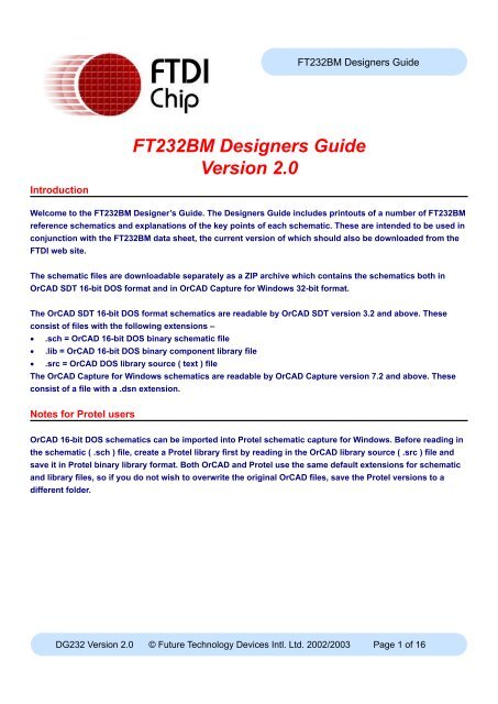
FT232BM Designers Guide - FTDI
FT232BM Designers Guide - FTDI
FT232BM Designers Guide - FTDI

You also want an ePaper? Increase the reach of your titles
YUMPU automatically turns print PDFs into web optimized ePapers that Google loves.
<strong>FT232BM</strong> <strong>Designers</strong> <strong>Guide</strong><strong>FT232BM</strong> <strong>Designers</strong> <strong>Guide</strong>Version 2.0IntroductionWelcome to the <strong>FT232BM</strong> Designer’s <strong>Guide</strong>. The <strong>Designers</strong> <strong>Guide</strong> includes printouts of a number of <strong>FT232BM</strong>reference schematics and explanations of the key points of each schematic. These are intended to be used inconjunction with the <strong>FT232BM</strong> data sheet, the current version of which should also be downloaded from the<strong>FTDI</strong> web site.The schematic files are downloadable separately as a ZIP archive which contains the schematics both inOrCAD SDT 16-bit DOS format and in OrCAD Capture for Windows 32-bit format.The OrCAD SDT 16-bit DOS format schematics are readable by OrCAD SDT version 3.2 and above. Theseconsist of files with the following extensions –• .sch = OrCAD 16-bit DOS binary schematic file• .lib = OrCAD 16-bit DOS binary component library file• .src = OrCAD DOS library source ( text ) fileThe OrCAD Capture for Windows schematics are readable by OrCAD Capture version 7.2 and above. Theseconsist of a file with a .dsn extension.Notes for Protel usersOrCAD 16-bit DOS schematics can be imported into Protel schematic capture for Windows. Before reading inthe schematic ( .sch ) file, create a Protel library first by reading in the OrCAD library source ( .src ) file andsave it in Protel binary library format. Both OrCAD and Protel use the same default extensions for schematicand library files, so if you do not wish to overwrite the original OrCAD files, save the Protel versions to adifferent folder.DG232 Version 2.0 © Future Technology Devices Intl. Ltd. 2002/2003 Page 1 of 16
<strong>FT232BM</strong> <strong>Designers</strong> <strong>Guide</strong>Figure 1.0 <strong>FT232BM</strong> – 5 volt Bus Powered Example Schematic ( 232-5VB )USBCN1CN-USB1234DECOUPLING CAPSVCCC310uFC20.1uFFB11 2VCCVCC VCCVCCFERRITE BEADC510nFR3470RC433nFC60.1uFU1VCC-5vRSTOUT#R4 27RR5 27RY16MHz RESONATORR6 1k552524232221201918TXDRXDRTS#CTS#5v MCU or Logic cct28VCC43212161514121110 SLEEP#POWERDN#31TESTRSTOUT#RESET#GND<strong>FT232BM</strong>C10.1uFVCCR22k21234U2CSSKDINDOUT93C46/56/66( Optional )VCCNCNCGND8765R110kFT232B APPLICATION SCHEMATICINTERFACING TO 5 V LOGIC - BUS POWERED (
<strong>FT232BM</strong> <strong>Designers</strong> <strong>Guide</strong>Figure 1.0 is an example of a 5 volt, USB bus powered design using the <strong>FT232BM</strong> connected to a 5v MCU orother external logic.• In this example, we assume that the total current of the design is
<strong>FT232BM</strong> <strong>Designers</strong> <strong>Guide</strong>Figure 2.0 <strong>FT232BM</strong> – 5 volt Self Powered Example Schematic ( 232-5VS )USBCN1CN-USB1234R610kDECOUPLING CAPSVCCC310uFC20.1uFVCC VCCVCCR4 27RR3470RR5 27RC433nFC50.1uFU1VCC-5vR71k5Y16MHz RESONATOR528432122524232221201918161514121110VCCSLEEP#TXDRXDRTS#CTS#5v MCU or Logic cctPOWERDN#31TESTGND<strong>FT232BM</strong>C10.1uFVCCR22k21234U2CSSKDINDOUT93C46/56/66( Optional )VCCNCNCGND8765VCCR110kFT232B APPLICATION SCHEMATICINTERFACING TO 5 V LOGIC - SELF POWERED APPLICATIONUPDATED 21st January 2003EXTERNAL 5V POWER529917302631368727RSTOUT#XTOUTRESET#EECSEESKEEDATATXDRXDRTS#CTS#DTR#DSR#DCD#RI#TXDENPWREN#PWRCTLTXLED#RXLED#SLEEP#AGNDGNDGNDAVCCVCCVCCVCC-IOR815k3V3OUTUSBDMUSBDPXTINC60.1uFVCCGNDDG232 Version 2.0 © Future Technology Devices Intl. Ltd. 2002/2003 Page 4 of 16
<strong>FT232BM</strong> <strong>Designers</strong> <strong>Guide</strong>Figure 2.0 is an example of a 5 volt, USB self powered design using the <strong>FT232BM</strong> connected to a 5v MCU orother external logic. A USB self power design has it’s own PSU and does not draw it’s power from the USBbus. In such a case, no special care need be taken to meet the USB suspend current ( 0.5mA ) as the devicedoes not get its power from the USB port.• In this case it is still useful to connect SLEEP# ( or PWREN# ) to the CPU as this will let the CPU knowthat the PC is in suspend mode and thus unable to communicate with the device. If the device requires to“wake up” the PC then the MCU should connect one of it’s IO Ports to the Ring Indicator pin ( RI# ). Thedefault state of RI# should be high - strobing this low for a few milliseconds then taking it high again willcause a USB resume sequence thus requesting the PC to wake up. To use this feature, Remote Wake-Upmust be enabled in the 93C46 EEPROM.• PWRCTL is tied to VCC to tell the device to indicate a self powered device in it’s USB descriptor.• RTS / CTS handshaking is used in this example. If the MCU has no dedicated handshaking signals thengeneral purpose IO pins can usually be used to implement the handshaking. If the MCU is guaranteed toaccept data sent from the <strong>FT232BM</strong> at the programmed baud rate, then a single wire handshake will do (tie CTS# of the <strong>FT232BM</strong> to GND ).• Self powered designs should NOT force current back into the Host PC ( or HUB ) via the USB Port whenthe said Host / Hub is powered down and the self powered device is still powered-up from it’s ownPSU. This rule includes injecting current into the powered down Host / Hub via the 1k5 pull-up on USBD+. Failure to do this can result in unreliable operation in the field. This is an integral part of the USBspecification and applies to all USB Self Powered devices ( not just <strong>FT232BM</strong> peripherals ). In this design,the presence of power on the host/hub USB port is used to control the RESET# pin of the <strong>FT232BM</strong>.When the Host / Hub is powered up RSTOUT# pulls the top end of the 1k5 resistor on USB D+ to 3.3vnominal thus identifying the device as a full speed device to USB. When the Host / HUB powers down,the <strong>FT232BM</strong> is reset and RSTOUT# will go low thus preventing current being injected into the Host / HubUSB D+ line via the 1k5 resistor.General Design Notes – See Previous ExampleDG232 Version 2.0 © Future Technology Devices Intl. Ltd. 2002/2003 Page 5 of 16
<strong>FT232BM</strong> <strong>Designers</strong> <strong>Guide</strong>Figure 3.0<strong>FT232BM</strong> – 5 volt Bus Powered Example Schematic with Power Switching ( 232-5VSW )USBCN1CN-USB1234DECOUPLING CAPSVCCC310uFC20.1uFFB11 2VCCFERRITE BEADC510nFR4 27RR5 27RY16MHz RESONATORC10.1uFVCCC433nFR6 1k5VCCR22k2R3470RC60.1uF52843212VCCSoft StartCircuitU12524232221201918<strong>FT232BM</strong>VCC1234U2CSSKDINDOUT93C46/56/66( Optional )VCCNCNCGND8765R110kFT232B APPLICATION SCHEMATICWITH POWER SWITCHINGPOWERED APPLICATIONVCC-5vTXDRXDRTS#CTS#5v MCU or Logic cctGND52991730263136872731Q1IRLML6402C80.1uFTXDRXDRTS#CTS#DTR#RSTOUT#DSR#DCD#RI#TXDEN16XTOUTPWREN#15RESET#PWRCTL14TXLED#12EECSRXLED#11EESKEEDATASLEEP#10AGNDGNDGNDAVCCVCCVCCVCC-IO3V3OUTUSBDMUSBDPXTINR71kTESTC70.1uFDG232 Version 2.0 © Future Technology Devices Intl. Ltd. 2002/2003 Page 6 of 16
<strong>FT232BM</strong> <strong>Designers</strong> <strong>Guide</strong>Figure 3.0 is an example of a 5 volt, USB bus powered design using the <strong>FT232BM</strong> connected to a 5v MCU orother external logic. In this design, the <strong>FT232BM</strong> controls the power to the auxiliary circuitry using PWEREN#to shut off power to this circuitry when –1. The <strong>FT232BM</strong> is in reset, OR2. The <strong>FT232BM</strong> has not yet been configured ( successfully recognised and enumerated over USB ), OR3. USB is in suspend / sleep mode.• A P-Channel Logic Level MOSFET is used as a power switch to control the power to the auxiliary devices– in this example we use a International Rectifier part number IRLML6402. R7 and C8 form a “soft start”circuit which limits the current surge when the MOSFET turns on. Without this, there is a danger that thetransient power surge of the MOSFET turning on will reset the <strong>FT232BM</strong> or the USB Host / Hub controller.The values used allow the attached circuitry to power up with a slew rate of ~ 12.5v per millisecond, inother words the output voltage will transitioning from GND to 5v in around 400uS.• When using this circuit, enable the “Pull-Down on Suspend” option in the EEPROM. This will ensureminimum leakage current during sleep ( suspend ) mode by gently pulling down the UART interface pinsof the <strong>FT232BM</strong> pins to GND during USB suspend.• The auxiliary circuitry attached to the <strong>FT232BM</strong> device must have it’s own power-on-reset circuitry andshould NOT use RESETO# to generate a reset for this circuitry. RESETO# does not generate a resetduring USB sleep ( suspend ) when the auxiliary logic is powered-off, thus cannot be used as a reset inthis case.• A “USB High-Power Bus Powered Device” ( one that consumes more than 100mA and up to 500mA )of current from the USB bus during normal operation must use this power control feature to remaincompliant as the USB specification does not allow a USB peripheral to draw more than 100mA of currentfrom the USB Bus until the device has been successfully enumerated. A “USB High-Power Bus PoweredDevice” cannot be plugged into a USB Bus-Powered Hub as these can only supply 100mA per USB port.• The Power ( current ) consumption of the device is set in a field in the 93C46 EEPROM attached to the<strong>FT232BM</strong>. A “USB High-Power Bus Powered Device” must use the 93C46 to inform the system of it’spower requirements.• PWRCTL is tied to GND to tell the device to indicate a bus powered device in it’s USB descriptor.• RTS / CTS handshaking is used in this example. If the MCU has no dedicated handshaking signals thengeneral purpose IO pins can usually be used to implement the handshaking. If the MCU is guaranteed toaccept data sent from the <strong>FT232BM</strong> at the programmed baud rate, then a single wire handshake will do (tie CTS# of the <strong>FT232BM</strong> to GND ).General Design Notes – See Previous ExamplesDG232 Version 2.0 © Future Technology Devices Intl. Ltd. 2002/2003 Page 7 of 16
<strong>FT232BM</strong> <strong>Designers</strong> <strong>Guide</strong>Figure 4.0 <strong>FT232BM</strong> – 3.3 volt Bus Powered Example Schematic ( 232-3VB )USBCN1CN-USBFB11 2VCCVCCVCC1234FERRITE BEADC510nFR3470RLDO REGULATOR 3.3vU3I OGC433nFC60.1uFU1RSTOUT#R4 27RR5 27RY16MHz RESONATORR6 1k552524232221201918VCCDECOUPLING CAPSVCC284321231161514121110SLEEP#RSTOUT#<strong>FT232BM</strong>C310uFC20.1uFC10.1uFVCCR22k21234U2CSSKDINDOUT93C46/56/66( Optional )VCCNCNCGND8765R110kFT232B APPLICATION SCHEMATICINTERFACING TO 3.3 V LOGIC - BUS POWERED (
<strong>FT232BM</strong> <strong>Designers</strong> <strong>Guide</strong>Figure 4.0 is an example of a 3.3 volt, USB bus powered design using the <strong>FT232BM</strong> connected to a 3.3v MCUor other external logic.• The main difference between this circuit and the 5 volt circuit of Figure 1.0 is that a 3.3 volt LDO regulatori.c. is used to provide a 3.3v supply to the auxiliary circuiry.• VCC-IO is driven from the 3.3v LDO regulator i.c. in order to drive the UART interface from the <strong>FT232BM</strong> tothe MCU / external logic at 3.3v level instead of 5v level.• As the USB supply rail can drop to 4.4 volts or less under load, an LDO ( Low Dropout ) voltage regulatormust be used in this instance.• The 3.3v LDO voltage regulator must also have a low quiescent ( no load ) current in order to ensure thatthe USB suspend current requirement (
<strong>FT232BM</strong> <strong>Designers</strong> <strong>Guide</strong>Figure 5.0 <strong>FT232BM</strong> – 3.3 volt Self Powered Example Schematic ( 232-3VS )USBCN1CN-USB1234R810kR715kDECOUPLING CAPSVCCC310uFC20.1uFVCCVCCR4 27RR3470RR5 27RC433nFC50.1uFU1R61k5Y16MHz RESONATOR52524232221201918284321216151412111031TEST<strong>FT232BM</strong>C10.1uFVCCR22k21234U2CSSKDINDOUT93C46/56/66( Optional )VCCNCNCGND8765R110kFT232B APPLICATION SCHEMATICINTERFACING TO 3.3V LOGIC - SELF POWERED APPLICATIONUPDATED 21st January 2003VCC3VVCC-3vTXDRXDRTS#CTS#3.3v MCU or Logic cctPOWEREN#GNDVCC VCC3VEXTERNAL POWER529917302631368727RSTOUT#TXDRXDRTS#CTS#DTR#DSR#DCD#RI#XTOUTRESET#EECSEESKEEDATATXDENPWREN#PWRCTLTXLED#RXLED#SLEEP#AGNDGNDGNDAVCCVCCVCCVCC-IO3V3OUTUSBDMUSBDPXTINC60.1uFVCC 3.3vVCC 5.0vGNDDG232 Version 2.0 © Future Technology Devices Intl. Ltd. 2002/2003 Page 10 of 16
<strong>FT232BM</strong> <strong>Designers</strong> <strong>Guide</strong>Figure 5.0 is an example of a 3.3 volt, USB self powered design using the <strong>FT232BM</strong> connected to a 3.3v MCUor other external logic. A USB self power design has it’s own PSU and does not draw it’s power from the USBbus. In such a case, no special care need be taken to meet the USB suspend current ( 0.5mA ) as the devicedoes not get its power from the USB port. The differences between this circuit and that of Figure 2.0 areminimal. See the notes in Figure 2 for the main details.• In this case the internal PSU needs to supply 3.3 volts to the auxiliary circuitry and 5 volts to the<strong>FT232BM</strong> i.c.• The VCCIO power line to the <strong>FT232BM</strong> is driven from the 3.3v supply in order to drive the auxiliary logic atthe correct voltage level.Important Note : In this design, the PWRCTL Pin ( Pin 14 ) of the <strong>FT232BM</strong> is tied high to indicate a selfpowered design. It is important to tie this to VCCIO ( 3.3v ) and NOT to VCC ( 5.0v ) otherwise the inputprotection diodes on this pin will conduct and try to pull VCCIO towards 5.0vAs well as being undesirable, this may cause excessive current to be drawn by the <strong>FT232BM</strong> and the 3.3vlogic attached to this device.DG232 Version 2.0 © Future Technology Devices Intl. Ltd. 2002/2003 Page 11 of 16
<strong>FT232BM</strong> <strong>Designers</strong> <strong>Guide</strong>Figure 6.0<strong>FT232BM</strong> – 3.3 volt Switched Power Bus Powered Schematic ( 232-3VSW)USBCN1CN-USB1234DECOUPLING CAPSVCCFB11 2FERRITE BEADVCCVCCVCCREG1TC55RP3302Q1C410nFR3470RG Vi VoIRLML6402C100.1uFSoft StartCircuitC333nFC90.1uFVCC-3vR4 27RR5 27RTXDRXDRTS#CTS#R6 1k55RSTOUT#Y16MHz RESONATORR71k3v MCU or Logic cctVCC4RESET#PWRCTL14GND<strong>FT232BM</strong>VCCR22k21234U2CSSKDINDOUT93C46/56/66( Optional )VCCNCNCGND8765R110kFT232B APPLICATION SCHEMATICINTERFACING TO 3.3 V LOGIC - BUS POWERED (
<strong>FT232BM</strong> <strong>Designers</strong> <strong>Guide</strong>Figure 6.0 is an example of a 3.3 volt, USB bus powered design with power switching using the <strong>FT232BM</strong>connected to a 3.3v MCU or other external logic. The circuit is essentially a combination of the schematics ofFigure 3 and Figure 4.• A 3.3 volt LDO regulator i.c. is used to provide a 3.3v VCCIO rail and switched 3.3v supply to the auxiliarycircuiry via a IRLML6402 P-Channel MOSFET .• In this example, we use a Telcom / MicroChip TC55RP3302 as the 3.3v LDO regulator. This has a maximumrated output current of 250mA. If a higher current is required, use an LD1117 / LM1117 series LDOregulator instead as these are rated to 800mA. The two are not pin compatible.• R7 and C10 form a soft start circuit which helps prevent excesssive power switching transients when theMOSFET turns on. We would advise you to include these components as without them the current surgewhen the IRLML6402 MOSFET initially turns on can be capable of resetting the <strong>FT232BM</strong> or tripping thepower sense circuitry in a USB hub.General Design Notes – See Previous ExamplesDG232 Version 2.0 © Future Technology Devices Intl. Ltd. 2002/2003 Page 13 of 16
<strong>FT232BM</strong> <strong>Designers</strong> <strong>Guide</strong>Figure 7.0 <strong>FT232BM</strong> –5v BUS Powered USB => RS232 Converter Example Schematic ( USB-232B )USBCN1CN-USB1234C1010nFFB11 2FERRITE BEADVCCC933nFVCCR5470RC110.1uFSHIELD RTS25 TXD RXDATAVCCD1TX LEDD2LED RXDSRRXD DCDRTS#CTS#DTR#DSR#DCD#RI#VCCR1220RVCCRIDTRCTSTXDATA594837261SKT1DB9MSHIELDDECOUPLING CAPSVCCU1TXD 72 TXDATADTR# 3 DTRRTS# RTSCTS 9CTS#DSRR1IN R1OUT84DSR#DCDR2IN R2OUT527DCD#RXDATAR3IN R3OUT262322 RXDSLEEP# RIR4IN R4OUT1819 RI#VCCR5IN R5OUT62021T1INT2INT3INT4INT1OUTT2OUTT3OUTT4OUT128VCCVCCC50.1uFSLEEP#VCC2524SHDN#EN13V+ V-17C70.1uFC410uFC30.1uFC10.1uFGNDC20.1uF93C46/56/66( Optional )VCCC60.1uF1214C1+C1-10GND VCC11MAX213CAIMAX213CWIADM213ESP213ECASP213EHCAC2+C2-1516C80.1uFFT232B APPLICATION SCHEMATICUSB RS232 SERIAL CONVERTER ( 300 to 115k/460k baud )VCC1055U224232221201918R2220R284321216151412111031<strong>FT232BM</strong>299173032613687273V3OUTRSTOUT#TXDRXDRTS#CTS#DTR#DSR#DCD#RI#XTOUTRESET#EECSEESKEEDATATXDENPWREN#PWRCTLTXLED#RXLED#SLEEP#AGNDGNDGNDAVCCVCCVCCVCC-IOR6 27RR7 27RY16MHz RESONATORR81k5USBDMUSBDPXTINTESTR42k21234U3CSSKDINDOUTVCCNCNCGND8765R310kDG232 Version 2.0 © Future Technology Devices Intl. Ltd. 2002/2003 Page 14 of 16
<strong>FT232BM</strong> <strong>Designers</strong> <strong>Guide</strong>Figure 7.0 is an example of a 5 volt, USB bus powered design using the <strong>FT232BM</strong> connected to a TTL óRS232 level converter i.c .• For RS232 applications, the baud rate of the finished product is limited by the ac. driving characteristicsof the level converter i.c. rather than that of the <strong>FT232BM</strong>.• This example uses the popular “213” series of TTL to RS232 level converters. These devices have 4transmitters and 5 receivers in a 28 LD SSOP package and feature an in-built voltage converter to convertthe 5v ( nominal ) VCC to the +/- 9volts required by RS232. An important feature of these devices is theSHDN# pin which can power down the device to a low quiescent current during USB suspend mode• The device used in this schematic is a Sipex SP213EHCA which is capable of RS232 communicationat up to 500k baud. If a lower baud rate is acceptable, then several pin compatible alternatives areavailable such as Sipex SP213ECA , Maxim MAX213CAI and Analog Devices ADM213E which are goodfor communication at up to 115,200 baud. If a higher baud rate is desired, use a Maxim MAX3245CAI partwhich is capable of RS232 communication at rates of up to 1M baud.• Note : the MAX3245 is not pin compatible with the 213 series devices, also it’s SHDN pin is active high soconnect this to PWREN# instead of SLEEP#.DG232 Version 2.0 © Future Technology Devices Intl. Ltd. 2002/2003 Page 15 of 16
<strong>FT232BM</strong> <strong>Designers</strong> <strong>Guide</strong>Document Revision HistoryDG232B Version 1.0 – Initial document created 05 August 2002DG232B Version 1.1 - Created 06 August 2002• Added USB-232B applicationDG232B Version 2.0 - Created 19th May 2003• Corrected Pull Up Control Circuit for Self Powered Designs• Corrected connection of PWRCTL in 3.3v Self Powered Designs• Updated Schematic Drawings• Added 3.3v Switched Bus Powered reference schematicDisclaimer© Future Technology Devices International Limited , 2002 / 2003Neither the whole nor any part of the information contained in, or the product described in this manual, maybe adapted or reproduced in any material or electronic form without the prior written consent of the copyrightholder.This product and its documentation are supplied on an as-is basis and no warranty as to their suitability forany particular purpose is either made or implied.Future Technology Devices International Ltd. will not accept any claim for damages howsoever arising as aresult of use or failure of this product. Your statutory rights are not affected.This product or any variant of it is not intended for use in any medical appliance, device or system in whichthe failure of the product might reasonably be expected to result in personal injury.The information in this document may be subject to change without notice.Contact InformationFuture Technology Devices Intl. LimitedSt. George’s Studios93/97 St. George’s Road,Glasgow G3 6JA,United Kingdom.Tel : +44 ( 0 )141 353 2565Fax : +44 ( 0 )141 353 2656E-Mail ( Sales ) : sales@ftdichip.comE-Mail ( Support ) : support@ftdichip.comE-Mail ( General Enquiries ) : admin@ftdichip.comWeb Site URL : http://www.ftdichip.comAgents and Sales RepresentativesAt the time of writing our Sales Network covers over 50 different countries world-wide. Please visit the Sales Networkpage of our Web Site site for the contact details our distributor(s) in your country.DG232 Version 2.0 © Future Technology Devices Intl. Ltd. 2002/2003 Page 16 of 16