6N135 6N136 HCPL4502 OPTOCOUPLERS/OPTOISOLATORS
6n135, 6n136, hcpl4502 optocouplers/optoisolators - Next.gr
6n135, 6n136, hcpl4502 optocouplers/optoisolators - Next.gr
- No tags were found...

You also want an ePaper? Increase the reach of your titles
YUMPU automatically turns print PDFs into web optimized ePapers that Google loves.
<strong>6N135</strong>, <strong>6N136</strong>, <strong>HCPL4502</strong><br />
<strong>OPTOCOUPLERS</strong>/<strong>OPTOISOLATORS</strong><br />
SOES022A – JULY 1986 – REVISED APRIL 1998<br />
<br />
<br />
<br />
<br />
Compatible with TTL Inputs<br />
High-Speed Switching ...1 Mbit/s Typ<br />
Bandwidth ...2 MHz Typ<br />
High Common-Mode Transient<br />
Immunity . . . 1000 V/µs Typ<br />
High-Voltage Electrical<br />
Insulation . . . 3000 Vdc Min<br />
Open-Collector Output<br />
UL Recognized . . . File Number 65085<br />
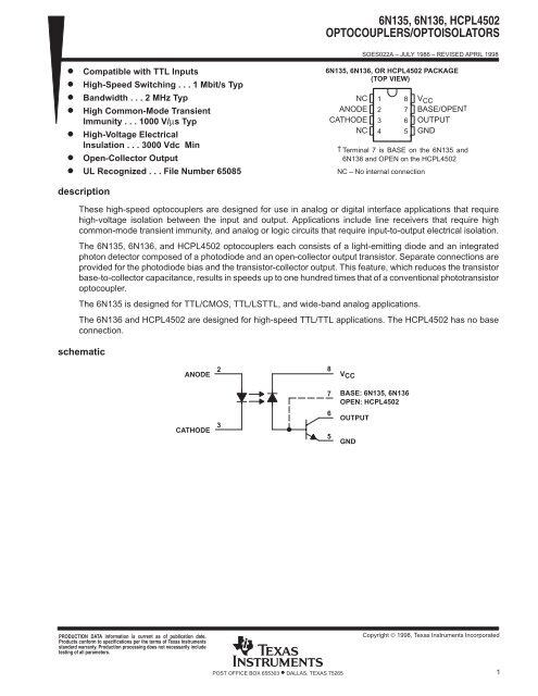
<strong>6N135</strong>, <strong>6N136</strong>, OR <strong>HCPL4502</strong> PACKAGE<br />
(TOP VIEW)<br />
NC<br />
ANODE<br />
CATHODE<br />
NC<br />
1<br />
2<br />
3<br />
4<br />
8<br />
7<br />
6<br />
5<br />
V CC<br />
BASE/OPEN †<br />
OUTPUT<br />
GND<br />
† Terminal 7 is BASE on the <strong>6N135</strong> and<br />
<strong>6N136</strong> and OPEN on the <strong>HCPL4502</strong><br />
NC – No internal connection<br />
description<br />
These high-speed optocouplers are designed for use in analog or digital interface applications that require<br />
high-voltage isolation between the input and output. Applications include line receivers that require high<br />
common-mode transient immunity, and analog or logic circuits that require input-to-output electrical isolation.<br />
The <strong>6N135</strong>, <strong>6N136</strong>, and <strong>HCPL4502</strong> optocouplers each consists of a light-emitting diode and an integrated<br />
photon detector composed of a photodiode and an open-collector output transistor. Separate connections are<br />
provided for the photodiode bias and the transistor-collector output. This feature, which reduces the transistor<br />
base-to-collector capacitance, results in speeds up to one hundred times that of a conventional phototransistor<br />
optocoupler.<br />
The <strong>6N135</strong> is designed for TTL/CMOS, TTL/LSTTL, and wide-band analog applications.<br />
The <strong>6N136</strong> and <strong>HCPL4502</strong> are designed for high-speed TTL/TTL applications. The <strong>HCPL4502</strong> has no base<br />
connection.<br />
schematic<br />
ANODE<br />
2<br />
8<br />
VCC<br />
CATHODE<br />
3<br />
7<br />
6<br />
5<br />
BASE: <strong>6N135</strong>, <strong>6N136</strong><br />
OPEN: <strong>HCPL4502</strong><br />
OUTPUT<br />
GND<br />
PRODUCTION DATA information is current as of publication date.<br />
Products conform to specifications per the terms of Texas Instruments<br />
standard warranty. Production processing does not necessarily include<br />
testing of all parameters.<br />
Copyright © 1998, Texas Instruments Incorporated<br />
POST OFFICE BOX 655303 • DALLAS, TEXAS 75265<br />
1
<strong>6N135</strong>, <strong>6N136</strong>, <strong>HCPL4502</strong><br />
<strong>OPTOCOUPLERS</strong>/<strong>OPTOISOLATORS</strong><br />
SOES022A – JULY 1986 – REVISED APRIL 1998<br />
absolute maximum ratings at 25°C free-air temperature (unless otherwise noted) †‡<br />
Supply and output voltage range, V CC and V O . . . . . . . . . . . . . . . . . . . . . . . . . . . . . . . . . . . . . . . . –0.5 V to 15 V<br />
Reverse input voltage . . . . . . . . . . . . . . . . . . . . . . . . . . . . . . . . . . . . . . . . . . . . . . . . . . . . . . . . . . . . . . . . . . . . . . . 5 V<br />
Emitter-base reverse voltage . . . . . . . . . . . . . . . . . . . . . . . . . . . . . . . . . . . . . . . . . . . . . . . . . . . . . . . . . . . . . . . . . 5 V<br />
Peak input forward current (pulse duration = 1 ms, 50% duty cycle, see Note 1) . . . . . . . . . . . . . . . . . . 50 mA<br />
Peak transient input forward current (pulse duration 1 µs, 300 Hz) . . . . . . . . . . . . . . . . . . . . . . . . . . . . . . . . . 1 A<br />
Average forward input current(see Note 2) . . . . . . . . . . . . . . . . . . . . . . . . . . . . . . . . . . . . . . . . . . . . . . . . . . 25 mA<br />
Peak output current . . . . . . . . . . . . . . . . . . . . . . . . . . . . . . . . . . . . . . . . . . . . . . . . . . . . . . . . . . . . . . . . . . . . . . 16 mA<br />
Average output current . . . . . . . . . . . . . . . . . . . . . . . . . . . . . . . . . . . . . . . . . . . . . . . . . . . . . . . . . . . . . . . . . . . . 8 mA<br />
Base current . . . . . . . . . . . . . . . . . . . . . . . . . . . . . . . . . . . . . . . . . . . . . . . . . . . . . . . . . . . . . . . . . . . . . . . . . . . . . 5 mA<br />
Input power dissipation at (or below) 70°C free-air temperature (see Note 3) . . . . . . . . . . . . . . . . . . . . . 45 mW<br />
Output power dissipation at (or below) 70°C free-air temperature (see Note 4) . . . . . . . . . . . . . . . . . . 100 mW<br />
Storage temperature range, T stg . . . . . . . . . . . . . . . . . . . . . . . . . . . . . . . . . . . . . . . . . . . . . . . . . . . –55°C to 125°C<br />
Operating free-air temperature range, T A . . . . . . . . . . . . . . . . . . . . . . . . . . . . . . . . . . . . . . . . . . . –55°C to 100°C<br />
Lead temperature 1,6 mm (1/16 inch) from case for 10 seconds . . . . . . . . . . . . . . . . . . . . . . . . . . . . . . . 260°C<br />
† Stresses beyond those listed under “absolute maximum ratings” may cause permanent damage to the device. These are stress ratings only, and<br />
functional operation of the device at these or any other conditions beyond those indicated under “recommended operating conditions” is not<br />
implied. Exposure to absolute-maximum-rated conditions for extended periods may affect device reliability.<br />
‡ JEDEC registered data for <strong>6N135</strong> and <strong>6N136</strong><br />
NOTES: 1. Derate linearly above 70°C free-air temperature at the rate of 1.67 mA/°C.<br />
2. Derate linearly above 70°C free-air temperature at the rate of 0.83 mA/°C.<br />
3. Derate linearly above 70°C free-air temperature at the rate of 1.50 mW/°C.<br />
4. Derate linearly above 70°C free-air temperature at the rate of 3.33 mW/°C.<br />
2 POST OFFICE BOX 655303 • DALLAS, TEXAS 75265
<strong>6N135</strong>, <strong>6N136</strong>, <strong>HCPL4502</strong><br />
<strong>OPTOCOUPLERS</strong>/<strong>OPTOISOLATORS</strong><br />
SOES022A – JULY 1986 – REVISED APRIL 1998<br />
electrical characteristics over operating free-air temperature range of 0°C to 70°C (unless<br />
otherwise noted)<br />
PARAMETER<br />
TEST CONDITIONS<br />
<strong>6N135</strong><br />
<strong>6N136</strong>, <strong>HCPL4502</strong><br />
MIN TYP† MAX MIN TYP† MAX<br />
VF ‡ Input forward voltage IF = 16 mA, TA = 25°C 1.6 1.7 1.6 1.7 V<br />
∝VF<br />
Temperature coefficient of<br />
forward voltage<br />
UNIT<br />
IF = 16 mA –1.8 –1.8 mV/°C<br />
VBR ‡ Input breakdown voltage IR = 10 µA, TA = 25°C 5 5 V<br />
VCC = 4.5 V, IOL = 1.1 mA 0.1 0.4<br />
VOL Low-level output voltage IF = 16 mA,<br />
IB = 0 IOL = 2.4 mA 0.1 0.4<br />
IF = 0, VCC = VO = 5.5 V 3 500 3 500 nA<br />
IOH ‡ High-level output current IB = 0,<br />
TA = 25°C VCC = VO = 15 V 0.01 1 0.01 1 µA<br />
IOH<br />
ICCH ‡<br />
ICCH<br />
ICCL<br />
hFE<br />
CTR‡<br />
CTR<br />
rIO<br />
IIO ‡<br />
High-level output current<br />
Supply current, high-level<br />
output<br />
Supply current, high-level<br />
output<br />
Supply current, low-level<br />
output<br />
Transistor forward current<br />
transfer ratio<br />
Current transfer ratio<br />
Current transfer ratio<br />
Input-output resistance<br />
Input-output insulation<br />
leakage current<br />
VCC = 15 V,<br />
IF = 0,<br />
VCC = 15 V,<br />
IF = 0,<br />
TA = 25°C<br />
VCC = 15 V,<br />
IF = 0,<br />
VCC = 15 V,<br />
IF = 16 mA,<br />
VO = 15 V,<br />
IB = 0<br />
V<br />
50 50 µA<br />
IO = 0,<br />
IB = 0, 0.02 1 0.02 1 µA<br />
IO = 0,<br />
IB = 0<br />
IO = 0,<br />
IB = 0<br />
VO = 5 V, IO = 3 mA 100<br />
VCC = 4.5 V,<br />
IF = 16 mA,<br />
TA = 25°C,<br />
VCC = 4.5 V,<br />
IF = 16 mA,<br />
See Note 5<br />
VIO = 500 V,<br />
See Note 6<br />
VIO = 3000 V,<br />
TA = 25°C,<br />
See Note 6<br />
2 2 µA<br />
40 40 µA<br />
100<br />
(<strong>6N136</strong><br />
only)<br />
VO = 0.4 V,<br />
IB = 0,<br />
See Note 5<br />
7% 18% 19% 24%<br />
VO = 0.5 V,<br />
IB = 0, 5% 15%<br />
TA = 25°C,<br />
1012 1012 Ω<br />
t = 5 s,<br />
RH = 45%, 1 1 µA<br />
Ci Input capacitance VF = 0, f = 1 MHz 60 60 pF<br />
Cio Input-output capacitance f = 1 MHz, See Note 6 0.6 0.6 pF<br />
† All typical values are at TA = 25°C.<br />
‡ JEDEC registered data for <strong>6N135</strong> and <strong>6N136</strong><br />
NOTES: 5. Current transfer ratio is defined as the ratio of output collector current IO to the forward LED input current IF times 100%.<br />
6. These parameters are measured with terminals 2 and 3 shorted together and terminals 5, 6, 7, and 8 shorted together.<br />
POST OFFICE BOX 655303 • DALLAS, TEXAS 75265<br />
3
<strong>6N135</strong>, <strong>6N136</strong>, <strong>HCPL4502</strong><br />
<strong>OPTOCOUPLERS</strong>/<strong>OPTOISOLATORS</strong><br />
SOES022A – JULY 1986 – REVISED APRIL 1998<br />
operating characteristics, V CC = 5 V, I F = 16 mA, T A = 25°C (unless otherwise noted)<br />
PARAMETER<br />
TEST CONDITIONS<br />
<strong>6N135</strong><br />
<strong>6N136</strong>, <strong>HCPL4502</strong><br />
MIN TYP MAX MIN TYP MAX<br />
BW Bandwidth (– 3 dB) RL = 100 Ω, See Note 7 2 2 MHz<br />
NOTE 7:<br />
Bandwidth is the range of frequencies within which the ac output voltage is not more than 3 dB below the low-frequency value.<br />
switching characteristics at V CC = 5 V, I F = 16 mA, T A = 25°C<br />
tPLH †<br />
tPHL †<br />
dV CM<br />
(H)<br />
dt<br />
PARAMETER<br />
Propagation delay<br />
time, low-to-highlevel<br />
output<br />
Propagation delay<br />
time, high-to-lowlevel<br />
output<br />
Common-mode<br />
input transient<br />
immunity,<br />
high-level output<br />
RL = 4.1 kΩ,<br />
See Figure 1<br />
RL = 1.9 kΩ,<br />
See Figure 1<br />
RL = 4.1 kΩ,<br />
See Figure 1<br />
RL = 1.9 kΩ,<br />
See Figure 1<br />
∆VCM = 10 V,<br />
RL = 4.1 kΩ,<br />
See Figure 2<br />
∆VCM = 10 V,<br />
RL = 1.9 kΩ,<br />
See Figure 2<br />
∆VCM = 10 V,<br />
See Notes 9 and 10,<br />
∆VCM = 10 V,<br />
See Notes 9 and 10,<br />
TEST CONDITIONS<br />
See Note 8,<br />
See Note 9,<br />
See Note 8,<br />
See Note 9,<br />
<strong>6N135</strong><br />
IF = 0,<br />
See Notes 8 and 10, 1000<br />
<strong>6N136</strong>, <strong>HCPL4502</strong><br />
MIN TYP MAX MIN TYP MAX<br />
1 1.5<br />
0.7 1.5<br />
IF = 0,<br />
See Notes 9 and 10, 1000<br />
0.6 0.8<br />
0.6 0.8<br />
Common-mode<br />
RL = 4.1 kΩ,<br />
1000<br />
dV input transient<br />
See Figure 2<br />
CM<br />
V/µs<br />
(L) immunity,<br />
dt<br />
RL = 1.9 kΩ,<br />
low-level output<br />
1000<br />
See Figure 2<br />
† JEDEC registered data for <strong>6N135</strong> and <strong>6N136</strong><br />
NOTES: 8. The 4.1-kΩ load represents one LSTTL unit load of 0.36 mA and a 6.1-kΩ pullup resistor.<br />
9. The 1.9-kΩ load represents one TTL unit load of 1.6 mA and a 5.6-kΩ pullup resistor.<br />
10. Common-mode transient immunity, high-level output, is the maximum rate of rise of the common-mode input voltage that does not<br />
cause the output voltage to drop below 2 V. Common-mode input transient immunity, low-level output, is the maximum rate of fall<br />
of the common-mode input voltage that does not cause the output voltage to rise above 0.8 V.<br />
UNIT<br />
UNIT<br />
µs<br />
µs<br />
V/µs<br />
4 POST OFFICE BOX 655303 • DALLAS, TEXAS 75265
<strong>6N135</strong>, <strong>6N136</strong>, <strong>HCPL4502</strong><br />
<strong>OPTOCOUPLERS</strong>/<strong>OPTOISOLATORS</strong><br />
PARAMETER MEASUREMENT INFORMATION<br />
SOES022A – JULY 1986 – REVISED APRIL 1998<br />
Pulse<br />
Generator<br />
ZO = 50 Ω<br />
tr = 5 ns<br />
RL<br />
5 V<br />
Output<br />
Input Current<br />
Monitor<br />
100 Ω<br />
Open<br />
CL = 15 pF<br />
(see Note A)<br />
GND<br />
TEST CIRCUIT<br />
Input<br />
Current<br />
IF<br />
0 V<br />
Output<br />
Voltage<br />
tPHL<br />
5 V<br />
1.5 V 1.5 V<br />
VOL<br />
tPLH<br />
NOTE A: CL includes probe and stray capacitance.<br />
WAVEFORMS<br />
Figure 1. Switching Test Circuit and Waveforms<br />
POST OFFICE BOX 655303 • DALLAS, TEXAS 75265<br />
5
<strong>6N135</strong>, <strong>6N136</strong>, <strong>HCPL4502</strong><br />
<strong>OPTOCOUPLERS</strong>/<strong>OPTOISOLATORS</strong><br />
SOES022A – JULY 1986 – REVISED APRIL 1998<br />
PARAMETER MEASUREMENT INFORMATION<br />
IF<br />
5 V<br />
RL<br />
B<br />
A<br />
Output<br />
VFF<br />
Open<br />
GND<br />
Generator<br />
TEST CIRCUIT<br />
Generator<br />
10 V<br />
90% 90%<br />
10% 10%<br />
tr<br />
tf<br />
0 V<br />
dVCM 8 V<br />
=<br />
dt tr or tf<br />
tr = 8 ns TYP<br />
tf = 8 ns TYP<br />
Output<br />
5 V<br />
Switch at A: IF = 0<br />
Output<br />
Switch at B: IF = 16 mA<br />
VOL<br />
VOLTAGE WAVEFORMS<br />
Figure 2. Transient Immunity Test Circuit and Waveforms<br />
6 POST OFFICE BOX 655303 • DALLAS, TEXAS 75265
<strong>6N135</strong>, <strong>6N136</strong>, <strong>HCPL4502</strong><br />
<strong>OPTOCOUPLERS</strong>/<strong>OPTOISOLATORS</strong><br />
TYPICAL CHARACTERISTICS<br />
SOES022A – JULY 1986 – REVISED APRIL 1998<br />
– Input-Diode Forward Current – mA<br />
IF<br />
20<br />
18<br />
16<br />
14<br />
12<br />
10<br />
8<br />
6<br />
4<br />
2<br />
INPUT-DIODE FORWARD CURRENT<br />
vs<br />
FORWARD VOLTAGE<br />
TA = 25°C<br />
0<br />
1.1 1.2 1.3 1.4 1.5 1.6 1.7<br />
VF – Forward Voltage – V<br />
– Output Current – mA<br />
I O<br />
12<br />
11<br />
10<br />
9<br />
8<br />
7<br />
6<br />
5<br />
4<br />
3<br />
2<br />
1<br />
<strong>6N135</strong><br />
CURRENT TRANSFER CHARACTERISTICS<br />
VCC = 5 V<br />
TA = 25°C<br />
0<br />
0 2 4 6 8 10 12<br />
VO – Output Voltage – V<br />
IF = 40 mA<br />
IF = 35 mA<br />
IF = 30 mA<br />
IF = 25 mA<br />
IF = 20mA<br />
IF = 15mA<br />
IF = 10mA<br />
IF = 5 mA<br />
14 16<br />
Figure 3<br />
Figure 4<br />
CTR – Current Transfer Ratio (Normalized)<br />
1.2<br />
1.1<br />
1<br />
0.9<br />
0.8<br />
0.7<br />
0.6<br />
0.5<br />
0.4<br />
CURRENT TRANSFER RATIO (NORMALIZED)<br />
vs<br />
INPUT DIODE FORWARD CURRENT<br />
<strong>6N136</strong><br />
<strong>HCPL4502</strong><br />
<strong>6N135</strong><br />
0.3<br />
VCC = 5 V<br />
0.2<br />
VO = 0.4 V<br />
0.1<br />
TA = 25°C<br />
Normalized to IF = 16 mA<br />
0<br />
1 2 4 7 10 20 40 70 100<br />
IF – Input Diode Forward Current – mA<br />
Figure 5<br />
CTR – Current Transfer Ratio (Normalized)<br />
1.1<br />
1<br />
0.9<br />
0.8<br />
0.7<br />
CURRENT TRANSFER RATIO (NORMALIZED)<br />
vs<br />
FREE-AIR TEMPERATURE<br />
VCC = 5 V<br />
VO = 0.4 V<br />
IF = 16 mA<br />
<strong>6N135</strong><br />
<strong>6N136</strong>,<br />
<strong>HCPL4502</strong><br />
0.6<br />
–60 –40 –20 0 20 40 60 80 100<br />
TA – Free-Air Temperature – °C<br />
Figure 6<br />
POST OFFICE BOX 655303 • DALLAS, TEXAS 75265<br />
7
<strong>6N135</strong>, <strong>6N136</strong>, <strong>HCPL4502</strong><br />
<strong>OPTOCOUPLERS</strong>/<strong>OPTOISOLATORS</strong><br />
SOES022A – JULY 1986 – REVISED APRIL 1998<br />
TYPICAL CHARACTERISTICS<br />
– High-Level Output Current – nA<br />
I OH<br />
10,000<br />
4000<br />
1000<br />
400<br />
100<br />
40<br />
10<br />
4<br />
1<br />
0.4<br />
HIGH-LEVEL OUTPUT CURRENT<br />
vs<br />
FREE-AIR TEMPERATURE<br />
VCC = 5 V<br />
VO = 5 V<br />
IF = 0<br />
0.1<br />
–75 –50 –25 0 25 50 75 100 125<br />
TA – Free-Air Temperature – °C<br />
Figure 7<br />
CTR(ac) – Differential Current Transfer Ratio – %<br />
DIFFERENTIAL CURRENT TRANSFER RATIO<br />
vs<br />
INPUT-DIODE QUIESCENT FORWARD CURRENT<br />
30<br />
25<br />
20<br />
15<br />
10<br />
5<br />
<strong>6N136</strong><br />
<strong>HCPL4502</strong><br />
<strong>6N135</strong><br />
0<br />
0 5 10 15 20<br />
IF – Input-Diode Quiescent Forward Current – mA<br />
Figure 8<br />
VCC = 5 V<br />
VO = 0.4 V<br />
TA = 25°C<br />
Frequency Response (Normalized)<br />
0<br />
–5<br />
–10<br />
–15<br />
–20<br />
FREQUENCY RESPONSE (NORMALIZED)<br />
vs<br />
FREQUENCY<br />
RL = 100 Ω<br />
RL = 220 Ω<br />
RL = 470 Ω<br />
RL = 1 kΩ<br />
–25<br />
IF = 16 mA<br />
TA = 25°C<br />
–30<br />
0.1 0.2 0.4 0.7 1 2 4 7 10<br />
f – Frequency – MHz<br />
t PLH , t PHL – Propagation Delay Time – µ s<br />
1.2<br />
1.1<br />
1<br />
0.9<br />
0.8<br />
0.7<br />
0.6<br />
0.5<br />
PROPAGATION DELAY TIME<br />
vs<br />
FREE-AIR TEMPERATURE<br />
VCC = 5 V<br />
IF = 16 mA<br />
RL = 4.1 kΩ for <strong>6N135</strong><br />
RL = 1.9 kΩ for <strong>6N136</strong><br />
<strong>6N136</strong> tPHL<br />
<strong>HCPL4502</strong><br />
<strong>6N136</strong> tPLH<br />
<strong>HCPL4502</strong><br />
<strong>6N135</strong> tPHL<br />
<strong>6N135</strong> tPLH<br />
0.4<br />
–60 –40 –20 0 20 40 60 80 100<br />
TA – Free-Air Temperature – °C<br />
Figure 9<br />
Figure 10<br />
8 POST OFFICE BOX 655303 • DALLAS, TEXAS 75265
<strong>6N135</strong>, <strong>6N136</strong>, <strong>HCPL4502</strong><br />
<strong>OPTOCOUPLERS</strong>/<strong>OPTOISOLATORS</strong><br />
MECHANICAL INFORMATION<br />
9,91 (0.390)<br />
9,49 (0.370)<br />
8 7 6 5<br />
SOES022A – JULY 1986 – REVISED APRIL 1998<br />
Index Dot<br />
L C<br />
7,87 (0.310)<br />
7,37 (0.290)<br />
6,60 (0.260)<br />
6,10 (0.240)<br />
C L<br />
1 2 3 4<br />
0,89 (0.035) MIN<br />
1,78 (0,070)<br />
1,14 (0.045)<br />
4,70 (0.185) MAX<br />
105°<br />
90°<br />
8 Places<br />
0,33 (0.013)<br />
0,18 (0.007)<br />
Seating Plane<br />
Gauge Plane<br />
0,76 (0.030)<br />
0,00 (0.000)<br />
3,17 (0.125) MIN<br />
0,51 (0.020)<br />
MIN<br />
1,40 (0.055)<br />
0,76 (0.030)<br />
2,79 (0.110)<br />
2,29 (0.090)<br />
0,84 (0.033) MIN<br />
8 Places<br />
0, 457 ± 0,076<br />
(0.018 ± 0.003)<br />
8 Places<br />
NOTES: A. JEDEC registered data. This data sheet contains all applicable registered data in effect at the time of publication.<br />
B. All linear dimensions are given in millimeters and parenthetically given in inches.<br />
Figure 11. Packaging Specifications<br />
POST OFFICE BOX 655303 • DALLAS, TEXAS 75265<br />
9
IMPORTANT NOTICE<br />
Texas Instruments (TI) reserves the right to make changes to its products or to discontinue any semiconductor<br />
product or service without notice, and advises its customers to obtain the latest version of relevant information<br />
to verify, before placing orders, that the information being relied on is current and complete.<br />
TI warrants performance of its semiconductor products and related software to the specifications applicable at<br />
the time of sale in accordance with TI’s standard warranty. Testing and other quality control techniques are<br />
utilized to the extent TI deems necessary to support this warranty. Specific testing of all parameters of each<br />
device is not necessarily performed, except those mandated by government requirements.<br />
Certain applications using semiconductor products may involve potential risks of death, personal injury, or<br />
severe property or environmental damage (“Critical Applications”).<br />
TI SEMICONDUCTOR PRODUCTS ARE NOT DESIGNED, INTENDED, AUTHORIZED, OR WARRANTED<br />
TO BE SUITABLE FOR USE IN LIFE-SUPPORT APPLICATIONS, DEVICES OR SYSTEMS OR OTHER<br />
CRITICAL APPLICATIONS.<br />
Inclusion of TI products in such applications is understood to be fully at the risk of the customer. Use of TI<br />
products in such applications requires the written approval of an appropriate TI officer. Questions concerning<br />
potential risk applications should be directed to TI through a local SC sales office.<br />
In order to minimize risks associated with the customer’s applications, adequate design and operating<br />
safeguards should be provided by the customer to minimize inherent or procedural hazards.<br />
TI assumes no liability for applications assistance, customer product design, software performance, or<br />
infringement of patents or services described herein. Nor does TI warrant or represent that any license, either<br />
express or implied, is granted under any patent right, copyright, mask work right, or other intellectual property<br />
right of TI covering or relating to any combination, machine, or process in which such semiconductor products<br />
or services might be or are used.<br />
Copyright © 1998, Texas Instruments Incorporated