Oscillators 02 - Learn About Electronics
Oscillators 02 - Learn About Electronics
Oscillators 02 - Learn About Electronics

Create successful ePaper yourself
Turn your PDF publications into a flip-book with our unique Google optimized e-Paper software.
Module<br />
2<br />
www.learnabout-electronics.org<br />
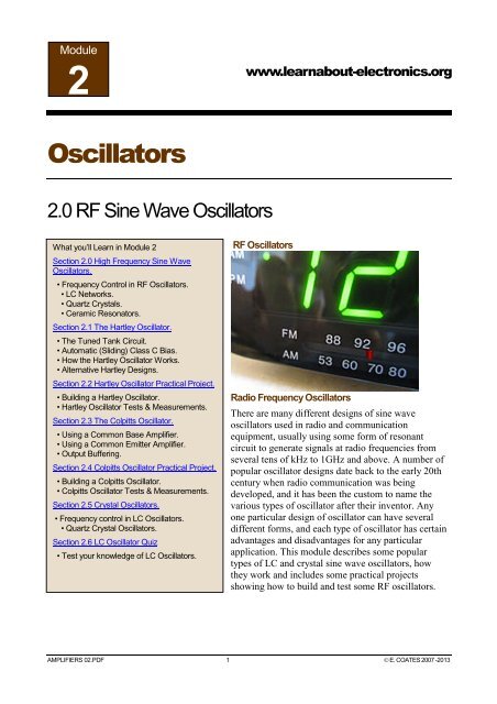
<strong>Oscillators</strong><br />
2.0 RF Sine Wave <strong>Oscillators</strong><br />
What you’ll <strong>Learn</strong> in Module 2<br />
Section 2.0 High Frequency Sine Wave<br />
<strong>Oscillators</strong>.<br />
• Frequency Control in RF <strong>Oscillators</strong>.<br />
• LC Networks.<br />
• Quartz Crystals.<br />
• Ceramic Resonators.<br />
Section 2.1 The Hartley Oscillator.<br />
• The Tuned Tank Circuit.<br />
• Automatic (Sliding) Class C Bias.<br />
• How the Hartley Oscillator Works.<br />
• Alternative Hartley Designs.<br />
Section 2.2 Hartley Oscillator Practical Project.<br />
• Building a Hartley Oscillator.<br />
• Hartley Oscillator Tests & Measurements.<br />
Section 2.3 The Colpitts Oscillator.<br />
• Using a Common Base Amplifier.<br />
• Using a Common Emitter Amplifier.<br />
• Output Buffering.<br />
Section 2.4 Colpitts Oscillator Practical Project.<br />
• Building a Colpitts Oscillator.<br />
• Colpitts Oscillator Tests & Measurements.<br />
Section 2.5 Crystal <strong>Oscillators</strong>.<br />
• Frequency control in LC <strong>Oscillators</strong>.<br />
• Quartz Crystal <strong>Oscillators</strong>.<br />
Section 2.6 LC Oscillator Quiz<br />
• Test your knowledge of LC <strong>Oscillators</strong>.<br />
RF <strong>Oscillators</strong><br />
Radio Frequency <strong>Oscillators</strong><br />
There are many different designs of sine wave<br />
oscillators used in radio and communication<br />
equipment, usually using some form of resonant<br />
circuit to generate signals at radio frequencies from<br />
several tens of kHz to 1GHz and above. A number of<br />
popular oscillator designs date back to the early 20th<br />
century when radio communication was being<br />
developed, and it has been the custom to name the<br />
various types of oscillator after their inventor. Any<br />
one particular design of oscillator can have several<br />
different forms, and each type of oscillator has certain<br />
advantages and disadvantages for any particular<br />
application. This module describes some popular<br />
types of LC and crystal sine wave oscillators, how<br />
they work and includes some practical projects<br />
showing how to build and test some RF oscillators.<br />
AMPLIFIERS <strong>02</strong>.PDF 1 © E. COATES 2007 -2013
www.learnabout-electronics.org <strong>Oscillators</strong> Module 2<br />
Frequency Control in RF <strong>Oscillators</strong><br />
Several different types of frequency control networks are used in high frequency sine wave<br />
oscillators. Three of the most commonly found are:<br />
1. LC Network, 2. Quartz Crystal, 3. Ceramic Resonator.<br />
LC Networks<br />
In networks, consisting of an inductors and capacitors the<br />
frequency of oscillation is inversely related to the values of L and<br />
C. (the higher the frequency, the smaller the values of L and C).<br />
LC oscillators generate a very good shape of sine wave and have<br />
quite good frequency stability. That is, the frequency does not<br />
change very much for changes in D.C. supply voltage or in<br />
ambient temperature. LC oscillators are extensively used for<br />
generating R.F. signals where good wave shape and reasonable<br />
frequency stability is required but is NOT of prime importance.<br />
Quartz Crystals<br />
Crystal oscillators are used to generate both square and sine<br />
waves at frequencies around 1 or 2 MHz and higher, when a very<br />
high degree of frequency stability is needed. The component<br />
determining the frequency of oscillation is thin slice of crystalline<br />
quartz (Silicon Dioxide), usually sealed inside a metal can. The<br />
quartz crystal vibrates mechanically at a very precise frequency<br />
when subjected to an alternating voltage. The frequency depends<br />
on the physical dimensions of the slice and the angle at which the<br />
slice is cut in relation to the atomic structure of the crystal, and so<br />
once the crystal has been manufactured to specific dimensions, its frequency is extremely accurate,<br />
and constant. The frequency produced is typically accurate to around 0.001% of its design<br />
frequency and is almost wholly independent of changes in supply voltage and variations in<br />
temperature over its working range. Where even greater accuracy is required, the crystal may be<br />
mounted in a small, heated and temperature controlled enclosure. Crystals are manufactured in a<br />
wide range of specific frequencies. Sine wave crystal oscillators are commonly used to generate<br />
very accurate frequency carrier waves in radio and other communications transmitters.<br />
Ceramic Resonators<br />
These components work in a similar way to quartz crystals, they<br />
vibrate when subjected to an AC signal, but are manufactured<br />
from a variety of ceramic materials. Thay are generally cheaper<br />
and physically smaller than equivalent quartz crystal resonators,<br />
but do not have such a high degreee of accuracy. They can be<br />
manufactured in either surface mount or through hole versions<br />
having either two or three connections.<br />
OSCILLATORS MODULE <strong>02</strong>.PDF 2 © E. COATES 2007-2013
www.learnabout-electronics.org <strong>Oscillators</strong> Module 2<br />
2.1 The Hartley Oscillator<br />
What you’ll learn in Module 2.1<br />
After Studying this section, you should be able to:<br />
• Understand the operation of The Tuned Tank Circuit.<br />
• Understand the operation of Automatic (Sliding) Class C Bias.<br />
• Understand the operation of Hartley <strong>Oscillators</strong>.<br />
• Recognise Alternative Hartley Designs.<br />
The Hartley Oscillator is a particularly useful circuit for<br />
producing good quality sine wave signals in the RF range,<br />
(30kHz to 30MHz) although at the higher limits of this<br />
range and above, The Colpitts oscillator is usually<br />
Fig. 2.1.1 The Hartley Oscillator<br />
preferred. Although both these oscillators oscillator use an<br />
LC tuned (tank) circuit to control the oscillator frequency, The Hartley design can be recognised by<br />
its use of a tapped inductor (L1 and L2 in Fig. 2.1.1).<br />
The frequency of oscillation can be calculated in the same way as any parallel resonant circuit,<br />
using:<br />
Where L = L1 + L2<br />
This basic formula is adequate where the mutual inductance between L1 and L2 is negligible but<br />
needs to be modified when the mutual inductance between L1 and L2 is considerable.<br />
Mutual Inductance in Hartley <strong>Oscillators</strong><br />
Mutual inductance is an additional effective<br />
amount of inductance caused by the magnetic<br />
field created around one inductor (or one part<br />
of a tapped inductor) inducing a current into<br />
the other inductor. When both inductors are<br />
wound on a common core, as shown in Fig.<br />
2.1.2 the effect of mutual inductance (M) can<br />
be considerable and the total inductance is<br />
calculated by the formula:<br />
L TOT =L 1 + L 2 ±2M<br />
Fig. 2.1.2 Centre Tapped Inductors on a<br />
Common Core<br />
OSCILLATORS MODULE <strong>02</strong>.PDF 3 © E. COATES 2007-2013
www.learnabout-electronics.org <strong>Oscillators</strong> Module 2<br />
The actual value of M depends on how effectively the two inductors are magnetically coupled,<br />
which among other factors depends on the spacing between the inductors, the number of turns on<br />
each inductor, the dimensions of each coil and the material of the common core.<br />
With separate fixed inductors, as shown in<br />
Fig. 2.1.3a considerations of mutual<br />
inductance are simplified, the dimensions and<br />
number of turns for each inductor are fixed,<br />
therefore main considerations are the physical<br />
distance between the inductors and the<br />
direction of their magnetic fields. In practice<br />
the small values of inductance of the inductors<br />
needed at RF create very little magnetic field<br />
outside the component and only when<br />
mounted within a couple of millimetres of<br />
each other is the mutual inductance effect<br />
noticeable, as shown in Fig. 2.1.3b.<br />
Fig. 2.1.3 Inductors with Adding Fields<br />
Whether M, measured in Henrys or more likely micro Henrys<br />
(µH) in RF oscillators adds to or subtracts from the total<br />
inductance of very closely mounted tapped inductors depends<br />
on the North-South polarity of the fields around the individual<br />
coils L 1 and L 2 , if the magnetic fields are both in the same<br />
direction, the mutual inductance will add to the total<br />
inductance but if the magnetic fields are arranged to oppose<br />
each other, as in Fig.2.1.4 the effect of the mutual inductance<br />
will be to reduce the total inductance and so increase the<br />
actual working frequency of the oscillator.<br />
Fig. 2.1.4 Inductors with<br />
Opposing Fields<br />
The amount of mutual inductance in a circuit using two small<br />
fixed inductors such as the circuit featured in <strong>Oscillators</strong> module 2.2 is minimal and experiments<br />
show that the inductors need to virtually touching to produce any noticeable effect. Whether the<br />
mutal inductance between small inductors of just a few micro Henrys add or subtract from the<br />
calculated oscillator frequency of a RF Hartley oscillator, this will generally only change the<br />
operating frequency by an amount similar to that which may be caused by the normal component<br />
value variation due to the values tolerances of the oscillator components.<br />
In practical Hartley oscillators that use inductors sharing a common core however, the mutual<br />
induction effect can be much greater, and depends on the coefficient of coupling (k), which has a<br />
value between 1 when the mutual inductance is just about equal to 100% magnetic coupling, and 0<br />
when there is no coupling between the two inductors.<br />
OSCILLATORS MODULE <strong>02</strong>.PDF 4 © E. COATES 2007-2013
www.learnabout-electronics.org <strong>Oscillators</strong> Module 2<br />
Calculating a theoretical value for k involves some quite complex<br />
math, due to the number of factors affecting the mutual coupling and<br />
the process is often reduced to deciding either there is little mutual<br />
coupling, such that less than half of the magnetic flux produce by one<br />
coil affects the other coil. Then k is assumed to have a value less than<br />
0.5, and the inductors are said to be ‘loosely coupled’ or if the<br />
inductors share a common core with zero spacing between them, they<br />
are said to be ‘tightly coupled’ and k is assumed to have a value<br />
between 0.5 and 1. In practice the core shared by such a tapped<br />
inductor working at RF frequencies will often be found to be a<br />
variable type as shown in Fig. 2.1.4 so that any frequency shift due to<br />
mutual inductance can be adjusted for by changing the position of the<br />
core and so correcting the oscillator frequency.<br />
The Hartley Circuit<br />
Fig. 2.1.1 shows a typical Hartley oscillator. The frequency determining resonant tuned circuit is<br />
formed by L1/L2 and C3 and is used as the load impedance of the amplifier. This gives the<br />
amplifier a high gain only at the resonant frequency (Method 2 in Introduction to <strong>Oscillators</strong>). This<br />
particular version of the Hartley circuit uses a common base amplifier, the base of TR1 being<br />
connected directly to 0V (as far as AC the signal is concerned) by C1. In this mode the output<br />
voltage waveform at the collector, and the input signal at the emitter are in phase. This ensures that<br />
the fraction of the output signal fed back from the tuned circuit collector load to the emitter via the<br />
capacitor C2 provides the necessary positive feedback.<br />
C2 also forms a long time constant with the emitter resistor R3 to provide an average DC voltage<br />
level proportional to the amplitude of the feedback signal at the emitter of Tr1. This is used to<br />
automatically control the gain of the amplifier to give the necessary closed loop gain of 1.<br />
The emitter resistor R3 is not decoupled because the emitter terminal is used as the amplifier input.<br />
The base being connected to ground via C1, which will have a very low reactance at the oscillator<br />
frequency.<br />
The Tuned LC (Tank) Circuit<br />
Fig. 2.1.5 Adjustable<br />
Ferrite Core<br />
The LC circuit that controls the frequency of<br />
oscillation is often called the "TANK CIRCUIT"<br />
because it contains circulating currents much greater<br />
than the current supplying it (e.g. pulses of collector<br />
current supplied by the amplifier). Its operation is<br />
supposed to be rather like a water tank or cistern that<br />
can supply a continuous flow of water from an<br />
intermittently flowing external supply. The tank<br />
circuit in the oscillator contains high values of<br />
circulating current topped up regularly by smaller<br />
amounts of current from the amplifier.<br />
Because most of the current flowing in the oscillator<br />
is flowing just around the resonant tank circuit rather<br />
than though the amplifier section of the oscillator, LC<br />
oscillators generally produce a sine wave with very<br />
little amplifier sourced distortion.<br />
Fig. 2.1.6 The Tank Circuit<br />
OSCILLATORS MODULE <strong>02</strong>.PDF 5 © E. COATES 2007-2013
www.learnabout-electronics.org <strong>Oscillators</strong> Module 2<br />
Another feature of the tank circuit is to provide the correct amount of positive feedback to keep the<br />
oscillator running. This is done by dividing the inductive branch of the circuit into two sections,<br />
each having a different value, the inductor therefore works in a similar manner to an<br />
autotransformer, the ratio of the two windings providing the appropriate amount of signal to be fed<br />
back to the input of the amplifier.<br />
Because in Fig. 2.1.6 (and Fig. 2.1.1) the top of L1 is connected to +Vcc, it is, as far as AC signals<br />
are concerned, connected to ground via the very low impedance of C5. Therefore waveform X<br />
across L1, and waveform Y across the whole circuit are in phase. As a common base amplifier is<br />
being used, the collector and emitter signals are also in phase, and the tank circuit is therefore<br />
providing positive feedback. In other Hartley designs, using common emitter amplifiers for<br />
example, similar tank circuits are used but with different connections, so that the feedback signal is<br />
always in phase with the input signal, therefore providing the necessary positive feedback.<br />
Automatic ‘Sliding’ Class C bias<br />
It is common in LC sine wave oscillators<br />
to use automatic class C bias. In class C<br />
the bias voltage, that is the base voltage<br />
of the transistor is more negative than the<br />
emitter voltage, making V be negative so<br />
that the average (centre) voltage of the<br />
input wave is located on the negative<br />
portion of the V be axis of the<br />
characteristic curve shown in Fig. 2.1.7<br />
Therefore only a portion of each sine<br />
wave is amplified to produce pulses of<br />
collector current.<br />
Fig. 2.1.7 Sliding Class C Bias<br />
OSCILLATORS MODULE <strong>02</strong>.PDF 6 © E. COATES 2007-2013
www.learnabout-electronics.org <strong>Oscillators</strong> Module 2<br />
Because only the tips of the waveform are amplified in class C, the amplifier cannot produce an<br />
undistorted output wave. This does not matter however, in an LC oscillator. All the amplifier is<br />
required to do is to provide pulses of current to the LC resonant circuit at its resonating frequency.<br />
The sine wave output of the circuit is actually produced by the resonating action of the LC circuit.<br />
The amplitude of the signal produced will depend on the amount of current flowing in the LC tuned<br />
circuit.<br />
As the amplifier provides this current it follows that, by automatically controlling the amount of<br />
collector current (I c ) flowing each time a pulse is produced, the amplitude of the output sine wave<br />
can be controlled at a constant level. The collector current of the transistor depends on the<br />
base/emitter voltage. In class C the base/emitter voltage is automatically varied so that the<br />
amplitude of the output wave remains stable.<br />
How the Hartley Oscillator Works<br />
The oscillator in Fig. 2.1.1 uses a common base amplifier. When the oscillator is first powered up,<br />
the amplifier is working in class A with positive feedback. The LC tank circuit receives pulses of<br />
collector current and begins to resonate at its designed frequency. The current magnification<br />
provided by the tank circuit is high, which initially makes the output amplitude very large.<br />
However, once the first pulses are present and are fed back to the emitter via C2, a DC voltage,<br />
dependent to a large extent on the time constant of C2 and R3, which is much longer than the<br />
periodic time of the oscillator wave, builds up across R3.<br />
As the emitter voltage increases, the bias point of the amplifier ‘slides’ from its class A position<br />
towards class C conditions, as shown in Fig 2.1.7, reducing the difference (V be ) between the<br />
relatively stable base voltage created by the potential diver Rl/R2 and the increasingly positive<br />
emitter voltage. This reduces the portion of the waveform that can be amplified by TR1, until just<br />
the tips of the waveform are producing pulses of collector current through the tank circuit and the<br />
closed loop gain circuit has reduced to 1. Effectively the positive feedback from the tank circuit and<br />
the negative and feedback created by C2 and R3 are in balance.<br />
Any deviation from this balance creates a correcting effect. If the amplitude of the output wave<br />
reduces, the feedback via C2 also reduces causing the emitter voltage to decrease, making negative<br />
value of V be smaller, and so creating a correcting increase in collector current and a greater output<br />
wave produced across the tank circuit. As collector current increases, then so will TR1 emitter<br />
voltage. This will cause a larger voltage across R3 making the emitter more positive, effectively<br />
increasing the amount of negative base/emitter voltage of Tr1. This reduces collector current again,<br />
leading to a smaller output waveform being produced by the tank circuit and balancing the closed<br />
loop gain of the circuit at 1.<br />
OSCILLATORS MODULE <strong>02</strong>.PDF 7 © E. COATES 2007-2013
www.learnabout-electronics.org <strong>Oscillators</strong> Module 2<br />
Alternative Hartley Designs.<br />
The circuit shown in Fig. 2.1.8 uses a common<br />
emitter amplifier and positive feedback from the<br />
top of the tuned circuit, via C2 (DC blocking<br />
and AC coupling capacitor) to the base.<br />
The top and bottom ends of the tapped inductor<br />
L1/L2 are in anti-phase as in this design, the<br />
tapping point of the tank circuit is connected to<br />
the supply line, which in a common emitter<br />
amplifier it is exactly the same point as the<br />
transistor emitter due to the decoupling<br />
capacitors across the supply (not shown as they<br />
will be in the power supply), and C3 across the<br />
emitter resistor.<br />
The base in a common emitter amplifier is also<br />
in anti-phase with the collector waveform,<br />
resulting in positive feedback via C2. Automatic<br />
class C bias is again used but in this circuit the<br />
Fig. 2.1.8 Common Emitter Hartley<br />
Oscillator<br />
value of the emitter decoupling capacitor C3 will be critical, and smaller than in a normal class A<br />
amplifier. It will only partially decouple R3, the time constant of R3/C3 controlling the amount of<br />
class C bias applied.<br />
In Fig. 2.1.9 the tapping on the inductor is connected to ground rather than +Vcc, and two DC<br />
blocking capacitors are used to eliminate any DC from the tuned circuit. The collector load is now<br />
provided by a RF choke which simply provides a high impedance at the oscillator frequency.<br />
Automatic class C bias is provided for the common emitter amplifier in a similar manner to Fig.<br />
2.1.8. In this variation however, rather than using a tuned amplifier that amplifies only at the desired<br />
frequency, the amplifier here will operate over a wide range of frequencies.<br />
However placing the tuned tank circuit in the feedback path ensures that positive feedback only<br />
occurs at the resonant frequency of the tuned circuit.<br />
Fig. 2.1.9 Hartley Oscillator with Tuned<br />
Feedback<br />
OSCILLATORS MODULE <strong>02</strong>.PDF 8 © E. COATES 2007-2013
www.learnabout-electronics.org <strong>Oscillators</strong> Module 2<br />
2.2 Hartley Oscillator Practical Project<br />
What you’ll learn in Module 2.2<br />
After studying this section, you should be able to:<br />
• Build a Hartley Oscillator from given instructions.<br />
• Test a Hartley Oscillator for correct operation.<br />
• Take measurements on a Hartley Oscillator.<br />
Building The Hartley Oscillator<br />
Build The Hartley Oscillator shown in Fig 2.2.1 using<br />
either breadboard (proto board) as shown in Fig. 2.2.2 or<br />
on strip board as shown in Fig. 2.2.3. The frequency of<br />
the oscillator can be from around 560kHz to 1.7MHz<br />
depending on the value chosen for C3. Full<br />
Fig. 2.2.1 Hartley Oscillator<br />
constructional details to build the Hartley oscillator are<br />
given below. Test the oscillator by making the measurements described on the Hartley Oscillator<br />
Measurements sheet to verify the operation of the oscillator, using a multi-meter and oscilloscope.<br />
A really effective way to learn about Hartley oscillators!<br />
This Hartley oscillator produces a sine wave output in excess of 12Vpp at an approximate<br />
frequency set by the value chosen for C3. Any of the C3 optional values shown below should give<br />
reliable oscillation.<br />
The circuit will operate from a 9V battery, or a DC power supply of 9 to 12V. Supply current at 9V<br />
is around 20 to 30mA.<br />
The circuit can be built on breadboard for testing purposes. It may be found that the value of R3 is<br />
fairly critical, producing either a large distorted waveform or intermittent low/no output. To find the<br />
best value for R3, it could be temporarily replaced by a 470 ohm variable resistor for<br />
experimentation to find the value that gives the best wave shape and reliable amplitude.<br />
Components List<br />
TR1 = 2N3904<br />
C1, C2 & C4 = 47nF<br />
C3 = See C3 Options table.<br />
R1 = 10KΩ<br />
R2 = 1KΩ<br />
C3 Options<br />
Value Frequency<br />
1nF 1.7MHz<br />
2.2nF 1.2MHz<br />
4.7nF 877kHz<br />
10nF 563kHz<br />
R3 = 22Ω (or 470Ω variable)<br />
L1 = 1.2µH<br />
Fig. 2.2.2 Hartley Oscillator - Breadboard Version<br />
L2 = 6.8µH<br />
OSCILLATORS MODULE <strong>02</strong>.PDF 9 © E. COATES 2007-2013
www.learnabout-electronics.org <strong>Oscillators</strong> Module 2<br />
Stripboard Version<br />
Additional Components For Strip-board Version<br />
Strip board 9x25 holes<br />
3 way connection block (Optional)<br />
9V battery connector (Optional)<br />
Tinned copper wire (for links)<br />
Insulated flexible wire (for external connections)<br />
Construction on Stripboard<br />
1. On a piece of 9 x 25 hole strip-board, mark hole A1<br />
to ensure that counting the strips and holes for<br />
placing track cuts and components always starts<br />
from the same point<br />
Fig. 2.2.3 Hartley Oscillator - Stripboard Version<br />
2. Mark the holes where track cuts are to be made.<br />
Double check their correct position before cutting.<br />
3. Make the track cuts.<br />
4. Solder the wire links in place.<br />
5. Solder the components in place in the following<br />
order.<br />
6. Resistors.<br />
7. Inductors.<br />
8. Polyester capacitors.<br />
9. Transistor (check for correct e b c positions before<br />
soldering).<br />
Fig. 2.2.4 Hartley Oscillator - Stripboard Layout<br />
10. Electrolytic (check for correct polarity before soldering).<br />
11. Terminal Block.(This may be replaced by a 9V battery connector & and an output lead if preferred).<br />
12. Carefully check for any short circuits caused by solder bridging adjacent tracks, and for any poorly<br />
soldered joints.<br />
13. Connect up the power supply and connect an oscilloscope to the output.<br />
14. Adjust the 470Ω variable resistor (if used in place of R3) for best wave shape with reliable operation.<br />
15. Once the best position is found, remove the variable resistor and measure its value. It can then be<br />
replaced with a fixed resistor having a preferred value closest to the measured value.<br />
OSCILLATORS MODULE <strong>02</strong>.PDF 10 © E. COATES 2007-2013
www.learnabout-electronics.org <strong>Oscillators</strong> Module 2<br />
Hartley Oscillator Measurements<br />
Having built the Hartley oscillator, either on breadboard or strip-board, check that the circuit is<br />
oscillating satisfactorily by connecting the circuit to the 9V supply and. connecting an oscilloscope<br />
to the output terminals<br />
Voltage and Current Measurements<br />
Ensure the oscillator is producing a sine wave output, and then measure and record the values listed<br />
in Tables 1 and 2.<br />
Table 1 Table 2 Table 3<br />
Take the following measurements with<br />
the circuit oscillating in class C:<br />
The supply current<br />
Temporarily stop the oscillations by<br />
connecting a 0.47µF (non-polarised)<br />
capacitor across R3 and take the<br />
following measurements:<br />
The supply<br />
current<br />
The Peak to Peak<br />
Voltage<br />
DC Level of the<br />
Wave<br />
The supply voltage<br />
TR1 collector<br />
voltage<br />
Periodic Time (T) of<br />
the Wave<br />
TR1 collector<br />
voltage<br />
TR1 base voltage<br />
TR1 base voltage<br />
TR1 emitter<br />
voltage<br />
Frequency of the<br />
wave (1/T)<br />
Frequency of the<br />
wave calculated by<br />
ƒ= 1/ 2π√(LC)<br />
TR1 emitter voltage<br />
Waveform Measurements<br />
Reconnect the oscilloscope to TR1<br />
collector (not the circuit output<br />
terminal) and draw at least two cycles<br />
of the collector waveform on the grid.<br />
Enter the volts/division and<br />
time/division settings of the CRO in the<br />
spaces provided.<br />
From the waveform, calculate and<br />
record the values in Table 3.<br />
OSCILLATORS MODULE <strong>02</strong>.PDF 11 © E. COATES 2007-2013
www.learnabout-electronics.org <strong>Oscillators</strong> Module 2<br />
2.3 The Colpitts Oscillator<br />
What you’ll learn in Module 2.3<br />
After studying this section, you should be able to:<br />
• Understand the operation of a Common Base<br />
Colpitts Oscillator.<br />
• Understand the operation of a Common Emitter<br />
Colpitts Oscillator.<br />
• Understand the need for Output Buffering.<br />
Common Base Colpitts Oscillator<br />
Fig. 2.3.1 shows a typical Colpitts oscillator<br />
design. This circuit is very similar in operation to<br />
the Hartley oscillator described in <strong>Oscillators</strong><br />
Module 2.1 but the Colpitts LC tank circuit<br />
consists of a single inductor and two capacitors.<br />
The capacitors form in effect, a single 'tapped'<br />
capacitor instead of the tapped inductor used in the Hartley. The values of the two capacitors<br />
(connected in series) are chosen so their total capacitance in series (C TOT ), is given by:<br />
Fig. 2.3.1 The Common Base Colpitts Oscillator<br />
This gives the total capacitance necessary for the tank circuit to achieve parallel resonance at the<br />
required frequency. The frequency of oscillation is given by the same formula as for the Hartley<br />
oscillator:<br />
But here the value C is the calculated value of C2 and C3 in series (C TOT ).<br />
The individual values of C2 and C3 are chosen so that the ratio of the values produces the necessary<br />
proportion of feedback signal. However, the ratio of voltages across two capacitors in series is in<br />
inverse proportion to the ratio of the values, i.e. the smaller capacitor has the larger signal voltage<br />
across it. The main advantage of the Colpitts arrangement is that the single inductor in the tuned<br />
circuit removes the effect of any mutual inductance between two coils where the alternating<br />
magnetic field built up around one inductor induces a current into the their inductor. This would<br />
affect the total inductance of the coils and so changes the resonant frequency of the tuned circuit.<br />
OSCILLATORS MODULE <strong>02</strong>.PDF 12 © E. COATES 2007-2013
www.learnabout-electronics.org <strong>Oscillators</strong> Module 2<br />
Common Emitter Colpitts Oscillator<br />
The circuit in Fig. 2.3.2 is the Colpitts equivalent of the<br />
Common Emitter Hartley Oscillator described in<br />
<strong>Oscillators</strong> Module 2.1 (Fig.2.1.8). It uses a common<br />
emitter amplifier, and as the tuned (tank) circuit tapping<br />
point in this configuration is connected to ground, the<br />
tank circuit produces anti-phase waves at top and<br />
bottom of L2, which ensures the correct phase<br />
relationships for positive feed back between collector<br />
and base. The feedback is applied to the base via C1,<br />
which also acts as a DC block, preventing the higher<br />
voltage on L1 upsetting the base bias voltage.<br />
Note that the tank circuit (L2, C2 and C3) is connected<br />
to the supply rail (+Vcc) via L1. If the tank circuit were<br />
connected directly to the supply there could be no antiphase<br />
AC signal present at the top of the tank circuit,<br />
due to the DC supply being heavily decoupled by large capacitors in the DC power supply. An RF<br />
choke (L1) having a high impedance at the frequency of oscillation is therefore included between<br />
the tuned circuit and the supply. This allows for a signal voltage for feedback purposes to be<br />
developed across L1.<br />
Automatic class C bias is used, with the emitter in this circuit only partially decoupled by a small<br />
value of C5 to give the ‘sliding bias’ previously described.<br />
The Colpitts oscillator, like the Hartley is capable of giving an excellent sine wave shape, and also<br />
has the advantage of better stability at very high frequencies. It can be recognised by always having<br />
a "tapped capacitor"<br />
Remember:<br />
HartLey = tapped L<br />
Colpitts = tapped C<br />
Fig. 2.3.2 A Colpitts Oscillator using<br />
a Common Emitter Amplifier<br />
Sine wave oscillator design is complicated by the fact that any load placed on the output, by circuits<br />
that the output is supplying, effectively places a damping resistance across the tank circuit. As well<br />
as reducing the amplitude of the oscillator output by having the effect of reducing the Q factor of<br />
the tuned tank circuit, this can adversely affect both the wave shape and the frequency stability of<br />
the oscillator waveform.<br />
OSCILLATORS MODULE <strong>02</strong>.PDF 13 © E. COATES 2007-2013
www.learnabout-electronics.org <strong>Oscillators</strong> Module 2<br />
Buffered Colpitts Oscillator<br />
A common solution is to feed the oscillator output into<br />
an emitter follower buffer amplifier, as shown in Fig.<br />
2.3.2. The oscillator section of this circuit is a slightly<br />
different version of the Colpitts oscillator in shown in<br />
Fig. 2.3.1.<br />
The RF choke is now the load impedance for TR1 and<br />
the tank circuit is isolated from TR1 by two DC<br />
blocking capacitors, C1 and C4. Therefore this version<br />
of the Colpitts oscillator uses a tuned feedback path<br />
(Method 1 in <strong>Oscillators</strong> Module 1.1) rather than a<br />
tuned amplifier (Method 2) as in Fig. 2.3.1<br />
Fig. 2.3.2 Colpitts Oscillator with Buffer Stage<br />
The emitter follower stage (R4, TR2 and R5) has a very high input impedance, thus having little<br />
loading effect on the oscillator, and a very low output impedance allowing it to drive loads of only a<br />
few tens of ohms impedance.<br />
The frequency stability of oscillators can also be affected by variations in supply voltage. It is<br />
common therefore, where good frequency stability is required, to use a stabilised power supply.<br />
Oscillator supplies may also need extra decoupling capacitors to remove unwanted 'noise' from the<br />
supply. Stable amplitude is normally achieved by using automatic class C bias, provided in this<br />
circuit by only partially decoupling the emitter of TR1 by C5.<br />
OSCILLATORS MODULE <strong>02</strong>.PDF 14 © E. COATES 2007-2013
www.learnabout-electronics.org <strong>Oscillators</strong> Module 2<br />
2.4 Colpitts Oscillator Practical Project<br />
What you’ll learn in Module 2.4<br />
After studying this section, you should be able to:<br />
• Build a Colpitts Oscillator from given instructions.<br />
• Test the Colpitts Oscillator for correct operation.<br />
• Take measurements on a Colpitts Oscillator.<br />
Build a Colpitts Oscillator<br />
Fig. 2.4.1 Colpitts Oscillator<br />
Build the Colpitts oscillator shown using either breadboard (proto board) or strip board, and then<br />
test the oscillator’s operation using a multi meter and oscilloscope.<br />
Building and testing your own circuit is a really effective way to learn about oscillators!<br />
The Oscillator Circuit<br />
This Colpitts oscillator produces a sine wave output in<br />
excess of 12Vpp at an approximate frequency set by the<br />
values chosen for L1, C2 and C3. It will operate from a<br />
9V battery, or a DC power supply up to 12V. Supply<br />
current at 9V is around 20mA. The circuit can be built<br />
on breadboard for testing purposes, where it will be<br />
found that the value of R3 is fairly critical. This 68 ohm<br />
resistor could be replaced by a slightly higher or lower<br />
value to alter the amplifier gain for experimentation. The<br />
values given for the circuit should work reliably when<br />
built on strip-board.<br />
Components List<br />
TR1 = 2N3904<br />
C1 = 1µF<br />
C2 = 33nF<br />
C3 = 10nF<br />
C4 = 47nF<br />
C5 = 100nF<br />
R1 = 15KΩ<br />
R2 = 5.6KΩ<br />
R3 = 22Ω (or 470Ω variable)<br />
L1 = 3.3µH<br />
Fig. 2.4.2 Colpitts Circuit<br />
Construction on Breadboard (Protoboard)<br />
Fig. 2.4.3 Colpitts Oscillator - Breadboard Version<br />
Construct the circuit on breadboard and experiment with different component values. The values<br />
shown on the circuit schematic above should give reliable oscillation. Note how some values<br />
produce different amplitudes or better wave shapes. It should be possible to obtain a good sine wave<br />
with a peak to peak output amplitude even greater than the supply voltage. This is a particular<br />
feature of LC oscillators as the AC output voltage depends on the amount of current circulating<br />
around the tuned circuit at resonance. But remember that a larger output voltage will also mean a<br />
higher collector current.<br />
OSCILLATORS MODULE <strong>02</strong>.PDF 15 © E. COATES 2007-2013
www.learnabout-electronics.org <strong>Oscillators</strong> Module 2<br />
Colpitts Oscillator Construction on Stripboard<br />
Additional Components For Stripboard Version<br />
Strip board 9x25 holes<br />
3 way connection block (Optional)<br />
9V battery connector (Optional)<br />
Tinned copper wire (for links)<br />
Insulated flexible wire(for external connections)<br />
Construction - Stripboard Version<br />
1. On a piece of 9 x 25 hole strip-board, mark<br />
hole A1 to ensure that counting the strips and<br />
holes for placing track cuts and components<br />
always starts from the same point.<br />
2. Mark the holes where track cuts are to be<br />
made. Double check their correct position<br />
before cutting.<br />
3. Make the track cuts.<br />
4. Solder the wire links in place.<br />
Fig. 2.4.2 Colpitts Oscillator - Stripboard Version<br />
5. Solder the components in place in the following order.<br />
6. Resistors.<br />
7. Inductor.<br />
8. Polyester capacitors.<br />
9. Transistor (check for correct e b c positions before soldering).<br />
10. Electrolytic (check for correct polarity before soldering).<br />
11. Terminal Block.<br />
Double check for correct positions and values of components<br />
Carefully check for any short circuits made by solder bridging adjacent tracks, and for any poorly<br />
soldered joints.<br />
Connect up the power supply and connect an oscilloscope to the output.<br />
OSCILLATORS MODULE <strong>02</strong>.PDF 16 © E. COATES 2007-2013
www.learnabout-electronics.org <strong>Oscillators</strong> Module 2<br />
Colpitts Oscillator Measurements<br />
Having built the Colpitts oscillator, either on breadboard or strip-board, check that the circuit is<br />
oscillating satisfactorily by connecting the circuit to the 9V supply and. connecting an oscilloscope<br />
to the output terminals.<br />
Voltage and Current Measurements<br />
Ensure the oscillator is producing a sine wave output, and then measure and record the values listed<br />
in Tables 1 and 2.<br />
Table 1 Table 2 Table 3<br />
Take the following measurements with<br />
the circuit oscillating in class C:<br />
The supply current<br />
Temporarily stop the oscillations by<br />
connecting a 0.47µF (non-polarised)<br />
capacitor across L1 and take the<br />
following measurements:<br />
The supply<br />
current<br />
The Peak to Peak<br />
Voltage<br />
DC Level of the<br />
Wave<br />
The supply voltage<br />
TR1 collector<br />
voltage<br />
Periodic Time (T) of<br />
the Wave<br />
TR1 collector<br />
voltage<br />
TR1 base voltage<br />
TR1 base voltage<br />
TR1 emitter<br />
voltage<br />
Frequency of the<br />
wave (1/T)<br />
Frequency of the<br />
wave calculated by<br />
ƒ= 1/ 2π√(LC)<br />
TR1 emitter voltage<br />
Waveform Measurements<br />
Reconnect the oscilloscope to TR1<br />
collector (not the circuit output<br />
terminal) and draw at least two cycles<br />
of the collector waveform on the grid.<br />
Enter the volts/division and<br />
time/division settings of the CRO in<br />
the spaces provided.<br />
From the waveform, calculate and<br />
record the values in Table 3.<br />
OSCILLATORS MODULE <strong>02</strong>.PDF 17 © E. COATES 2007-2013
www.learnabout-electronics.org <strong>Oscillators</strong> Module 2<br />
2.5 Crystal Sine Wave <strong>Oscillators</strong><br />
What you’ll learn in Module 2.5<br />
After studying this section, you should be able to:<br />
• Understand the need for Frequency control in LC <strong>Oscillators</strong>.<br />
• Understand the application of Quartz Crystals in LC <strong>Oscillators</strong>.<br />
• Understand the operation of Quartz Crystals.<br />
• Understand the application of Quartz Crystals in both serial and<br />
parallel modes.<br />
• Recognise Integrated Crystal Oscillator Modules.<br />
Crystal Sine Wave <strong>Oscillators</strong><br />
Where good frequency stability is<br />
required, in applications such radio<br />
transmitters, basic LC oscillators<br />
cannot guarantee to hold their<br />
frequency without some drifting,<br />
which can be caused by quite small<br />
changes in supply voltage (although<br />
stabilised power supplies help avoid<br />
this) and changes in temperature.<br />
The effects of resistance and stray capacitance within the circuit can also cause the oscillator to<br />
operate at a slightly different frequency from that calculated using just the values of L and C. In<br />
most cases this can be overcome by making the tuned ‘tank’ circuit have as high a Q factor as<br />
possible. With ordinary inductors and capacitors, Q factors more than a few hundred are not<br />
possible, but by using quartz crystals Q factors well in excess of 10,000 can be achieved.<br />
Crystals may be used increase frequency<br />
stability in RF oscillators such as Hartley and<br />
Colpitts. The crystal may be used either in<br />
‘parallel mode’ e.g. as an inductor operating<br />
at a frequency between ƒ 1 and ƒ 2 as part of<br />
the resonating tuned circuit, as shown in the<br />
crystal controlled Colpitts oscillator in Fig<br />
2.5.1, or in ‘series mode’ where the crystal is<br />
acting as a highly selective low impedance at<br />
ƒ 1 in the feedback path as shown in a Hartley<br />
oscillator in Fig. 2.5.2.<br />
Fig. 2.5.1 Colpitts Oscillator using<br />
a Crystal in Parallel Mode<br />
The Quartz Crystal<br />
The quartz crystal is a piezo-electric device, and<br />
will both produce a voltage across it when it is<br />
subjected to some mechanical distortion such as<br />
slight bending, or will distort slightly when a<br />
voltage is applied across it. Therefore applying<br />
regular voltage pulses will cause the crystal to<br />
bend, and the bending will in turn create voltage<br />
pulses in phase with the applied pulses, that will<br />
reinforce them and cause oscillation.<br />
The frequency at which this reinforcing effect<br />
occurs is the resonant frequency of the crystal,<br />
Fig. 2.5.2 Hartley Oscillator using<br />
a Crystal in Series Mode<br />
and this is determined by the physical size of the crystal and by the way the crystal is cut in relation<br />
to its atomic structure. When a quartz crystal is accurately cut and prepared, it is almost perfectly<br />
elastic. This means that once oscillations start, they take a long time to die away.<br />
OSCILLATORS MODULE <strong>02</strong>.PDF 18 © E. COATES 2007-2013
www.learnabout-electronics.org <strong>Oscillators</strong> Module 2<br />
Fig 2.5.3 shows the circuit (schematic) symbol for a quartz crystal and its equivalent circuit. Notice<br />
that in effect it contains all of the properties (L, C and R) normally associated with a tuned circuit. It<br />
can therefore be used to replace either a series tuned circuit or a parallel tuned circuit, and the graph<br />
of its impedance (Z) shows two resonant frequencies ƒ 1 and ƒ 2 . When used in series mode the<br />
crystal exhibits very low impedance at ƒ 1 , and in parallel mode, a very high impedance at ƒ 2 . In<br />
practice, because of the extremely narrow bandwidth caused by the crystal’s very high Q factor,<br />
these frequencies are close enough together to be considered the same for many purposes.<br />
Crystal oscillators can produce either sine wave or<br />
square wave outputs over a very wide range of<br />
frequencies, usually from one or two MHz up to<br />
several hundred MHz. Crystals are produced to<br />
resonate at many different specific frequencies for<br />
particular applications, but the range of available<br />
frequencies is made much greater by various<br />
techniques such as frequency division, where the<br />
frequency of a crystal oscillator is sequentially divided<br />
by 2 many times by digital dividers, to a much lower<br />
frequency. Because any slight errors are also reduced<br />
by the same division process, the final low frequency<br />
is much more accurate.<br />
Fig. 2.5.3 The Quartz Crystal<br />
Crystals can also be made to resonate at higher multiples of their basic resonant frequency. One of<br />
these higher multiples, called overtones) can then be selected using a conventional LC circuit. By<br />
using these frequency division and overtone techniques a much wider range of crystal frequencies<br />
can be achieved.<br />
Integrated Crystal Oscillator Modules<br />
In modern circuitry it is far less common to find crystal oscillators constructed from discrete<br />
components, as many ready-made crystal oscillators are available. Both square wave and sine wave<br />
oscillators are available as DIL (dual in line) or SMT (surface mount) modules with a wide variety<br />
of specifications and frequencies.<br />
In sine wave oscillators for use in radio transmission, the<br />
oscillator is the source of the transmitted radio wave, so<br />
frequency accuracy and stability are of vital importance<br />
as radio bands are usually crowded with many<br />
transmitters operating in a given radio band. Transmitters<br />
therefore must not allow their transmission frequency to<br />
wander and interfere with adjacent transmissions.<br />
Receivers must be able to tune to known reliable<br />
frequencies.<br />
Fig. 2.5.4 14pin DIL Crystal<br />
Oscillator Module<br />
Many crystal oscillators are capable of maintaining their set frequency to within a few parts per<br />
million e.g +/- 5 to 50Hz for each MHz of their intended frequency, over temperature ranges<br />
typically from 0 to 70 degrees for consumer applications and -85 to +85 degrees for some military<br />
and aerospace specifications.<br />
OSCILLATORS MODULE <strong>02</strong>.PDF 19 © E. COATES 2007-2013
www.learnabout-electronics.org <strong>Oscillators</strong> Module 2<br />
Very low harmonic distortion is also an important factor.<br />
That is, the oscillator must not output frequencies at<br />
harmonics of the design frequency, as these would create<br />
extra transmissions at these frequencies. To avoid harmonic<br />
distortion, the sine wave must be as pure as possible and<br />
oscillators are available with a total harmonic distortion (the<br />
percentage of power in generated harmonics compared to the<br />
power generated in the fundamental sine wave) of just a few<br />
percent.<br />
Fig. 2.5.5 Typical Oscillator<br />
Module Connections<br />
Many oscillator modules have only 3 pins for +Vcc Ground and output, though some have extra<br />
pins for control options and typically drive loads such as 50 ohms with an output of 500mV to 1V<br />
as shown in Fig. 2.5.5.<br />
Because many of the characteristics of an oscillator vary with temperature, special oven controlled<br />
crystal oscillators (OCXOS) are made for the most critical applications. These oscillators are<br />
contained within a heated, thermostatically controlled case, so that in operation their temperature is<br />
kept at a constant level. This allows frequency variations to be kept typically below 1 part per<br />
million and harmonic distortion to less than 1%.<br />
OSCILLATORS MODULE <strong>02</strong>.PDF 20 © E. COATES 2007-2013
www.learnabout-electronics.org <strong>Oscillators</strong> Module 2<br />
2.6 RF <strong>Oscillators</strong> Quiz<br />
Try our quiz, based on the information you can find in <strong>Oscillators</strong> Module 2.<br />
You can check your answers by using the online version at:<br />
http://www.learnabout-electronics.org/<strong>Oscillators</strong>/osc26.php<br />
1. Refer to Fig. 2.6.1. Which of the following component combinations are responsible for providing Sliding Class<br />
C bias?<br />
a) R1, R2<br />
b) C1, R2<br />
c) C2, L2<br />
d) C2, R3<br />
2. Refer to Fig. 2.6.1. A typical frequency of oscillation for this circuit would be most likely to be in which of the<br />
following ranges?<br />
a) AF 20Hz to 20kHz<br />
b) RF 30kHz to 30MHz<br />
c) VHF 30MHz to 300MHz<br />
d) UHF 300MHz to 3GHz<br />
3. Which formula in Fig 2.6.2 should be used for finding the frequency of oscillation of a LC oscillator?<br />
a)<br />
b)<br />
c)<br />
d)<br />
4. Refer to Fig. 2.6.1. What will be phase relationship between the waveforms at points A and B?<br />
a) They will be in phase.<br />
b) They will be in antiphase.<br />
c) A will lead B by 90°.<br />
d) B will lead A by 90°.<br />
5. Refer to Fig. 2.6.3. Which of the following governs the proportion of signal used as positive feedback?<br />
a) The reactance of C1.<br />
b) The impedance of C4 at the frequency of oscillation.<br />
c) The time constant of R3,C4<br />
d) The value ratio of C2 to C3<br />
OSCILLATORS MODULE <strong>02</strong>.PDF 21 © E. COATES 2007-2013
www.learnabout-electronics.org <strong>Oscillators</strong> Module 2<br />
6.The output of a LC oscillator is often fed into a common collector amplifier stage. The reason for this is:<br />
a) To provide extra voltage gain.<br />
b) To provide negative feedback.<br />
c) To reduce loading on the tank circuit.<br />
d) To convert the sine wave output to a square wave.<br />
7. Refer to Fig. 2.6.3. Which of the following actions would increase the frequency of the oscillator?<br />
a) Increase the value of C2<br />
b) Decrease the value of C4<br />
c) Increase the value of R2<br />
d) Decrease the value of L1<br />
8. Refer to Fig. 2.6.4. What is the purpose of L1?<br />
a) To provide an antiphase signal for positive feedback.<br />
b) To provide an in phase signal for positive feedback.<br />
c) To correct the 90° phase shift produced by the tank circuit.<br />
d) To provide a load impedance for the output signal.<br />
9. A typical specification for a quartz crystal oscillator would indicate a Q factor of:<br />
a) Less than 500<br />
b) <strong>About</strong> 1,000<br />
c) <strong>About</strong> 5,000<br />
d) More than 10,000<br />
10. Refer to Fig. 2.6.5. In which of the following modes is the quartz crystal X1 operating?<br />
a) A high impedance parallel resonant circuit.<br />
b) A low impedance parallel resonant circuit.<br />
c) A high impedance series resonant circuit.<br />
d) A low impedance series resonant circuit.<br />
OSCILLATORS MODULE <strong>02</strong>.PDF 22 © E. COATES 2007-2013