

design brief - Steven Keating's
design brief - Steven Keating's
design brief - Steven Keating's

You also want an ePaper? Increase the reach of your titles
YUMPU automatically turns print PDFs into web optimized ePapers that Google loves.
nanocolumn InGaN photovoltaic <strong>design</strong><br />
Currently, the main obstacle to solar panel proliferation is cost. During the summer of 2009, I started work<br />
under Dr. Joshua Pearce looking at ways to improve photovoltaic efficiency and reduce material expenses.<br />
The topic of research was indium gallium nitride (InGaN), which is a new potential photovoltaic material.<br />
Both the optical and structural properties of InGaN were of interest as InGaN has been shown to have a<br />
tuneable band gap (from 0.4 eV to 3.4 eV depending on the indium content). This is an promising material,<br />
as most semiconductors used for solar cells have fixed band gaps and the band gap of a material dictates<br />
what frequencies of light the material can absorb. Most commercial solar cells are single-junction cells,<br />
meaning that only one band gap is used to collect solar energy. Newer, multi-junction cells function similarly<br />
to a stack of single-junction cells, and can collect a wider range of frequencies using different materials for<br />
each junction. These higher efficiencies multi-junction cells currently exist, but are expensive and require<br />
careful processing to get the different materials to have proper lattice matching. InGaN offers a unique<br />
opportunity, as a multi-junction cell could be made with all of the junctions containing InGaN. The different<br />
junctions would only have to have slightly varying compositions of indium to achieve the required varying<br />
band gaps. This means lattice matching would be significantly easier, and the material costs are<br />
inexpensive compared to the high-purity silicon currently used.<br />
While the main driving factor for solar InGaN research is the tuneable band gap, another interesting avenue<br />
is the microstructure. This past summer, my work revealed the nanocolumnar growth present in our method<br />
of InGaN deposition. These nanocolumns offer an interesting method to easily creating a three-dimensional<br />
solar cell. If the columnar structure could be maintained in a solar cell, the extra surface area and reflection<br />
properties will improve absorption and efficiency when compared to the standard planar geometry. The<br />
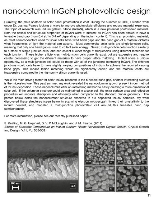
photos below detail the nanocolumnar structure observed in our deposited InGaN samples. My work<br />
discovered these structures (seen below in scanning electron microscopy), linked their crystallinity to the<br />
indium content, and modeled a multi-junction photovoltaic cell around this tuneable band gap<br />
semiconductor.<br />
For more information, please see our recently published paper:<br />
S. Keating, M. G. Urquhart, D. V. P. McLaughlin, and J. M. Pearce. (2011)<br />
Effects of Substrate Temperature on Indium Gallium Nitride Nanocolumn Crystal Growth. Crystal Growth<br />
and Design. V.11, Pg. 565-568<br />
11