

Technologies
fast16_full_proceedings
fast16_full_proceedings

Create successful ePaper yourself
Turn your PDF publications into a flip-book with our unique Google optimized e-Paper software.
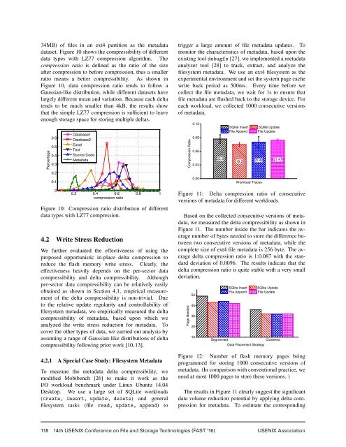
e intuitively justified. When both the original data and<br />
delta information cannot be compressed efficiently (such<br />
as R data is 0.7 and R delta is 0.6), the write stress can be<br />
hardly reduced because the compressed delta cannot be<br />
placed in the same page with the original data. However,<br />
with the clustered data placement strategy, some deltas<br />
could be placed because of a larger shared spare space.<br />
Thus the clustered data placement strategy has a better<br />
performance than the segmented approach in most of<br />
the cases, especially when the compression efficiency is<br />
relatively poor.<br />
The write stress reduction varies among different<br />
workloads and strongly depends on the data update operation<br />
frequency. For example, with a large percentage<br />
of data updates than “Homes”, “Repeated File Update”<br />
can achieve noticeably better write stress reduction as<br />
shown in Figure 13. In essence, there exists a upper<br />
bound of write stress reduction, which is proportional to<br />
the percentage of update operations. This explains why<br />
the write stress reduction cannot be further noticeably<br />
reduced even with better data compressibility, as shown<br />
in Figure 13.<br />
4.3 Implementation Overhead Analysis<br />
This subsection discusses and analyzes the overhead<br />
caused by the proposed design solution in terms of read<br />
latency, update latency, and SSD controller silicon cost.<br />
4.3.1 Read Latency Overhead<br />
Figure 14 illustrates the read process to recover the<br />
latest data content. After the flash memory sensing<br />
and flash-to-controller data transfer, the SSD controller<br />
parses the data elements and accordingly carries out<br />
the ECC decoding and data/delta decompression, based<br />
upon which it combines the original data and all the<br />
subsequent deltas to obtain the latest data content.<br />
As explained in Section 3.2, different segments are<br />
protected by different ECC codes (LDPC codes or<br />
BCH codes) according to the length of information bits.<br />
Hence the controller must contain several different ECC<br />
decoders.<br />
sen<br />
Memory<br />
Sensing<br />
<br />
xfer<br />
Data<br />
Transfer<br />
ecc<br />
LDPC<br />
Decode<br />
BCH<br />
Decode<br />
dec<br />
Decompress<br />
Decompress<br />
com<br />
Combine<br />
sata<br />
SATA<br />
Transfer<br />
Figure 14: Illustration the process to obtain the latest data<br />
content.<br />
Let τ sen denote the flash memory sensing latency(the<br />
latency to read out the data content from flash cells using<br />
sensing circuits [29]), τ x f er (Ω) denote the latency of<br />
transferring Ω amount of data from flash memory chip to<br />
delta<br />
SSD controller, τ (dec)<br />
LDPC<br />
and τ(dec)<br />
BCH<br />
denote the LDPC and<br />
BCH decoding latency, τ sec<br />
(dec) and τ (dec) denote the latency<br />
of decompressing the original data and deltas, τ com<br />
denote the latency to combine the original data and all<br />
the deltas to obtain the latest data content, and τ sata denote<br />
the latency of transferring 4kB from SSD to host.<br />
In the conventional design practice without delta compression,<br />
to serve a single 4kB read request, the overall<br />
latency can be expressed as:<br />
τ read = τ sen + τ x f er (4kB)+τ (dec)<br />
LDPC + τ sata. (1)<br />
When using the proposed design solution to realize<br />
delta compression, the read latency can be expressed as:<br />
τ read =τ sen + τ x f er (n · 4kB)+max(τ (dec)<br />
LDPC ,τ(dec) BCH )<br />
+ max(τ sec<br />
(dec) ,τ (dec)<br />
delta )+τ com + τ sata ,<br />
where n denotes the number of 4kB sectors being<br />
transferred from flash memory chip to SSD controller.<br />
We have that n = 1 in the case of segmented placement,<br />
and n is the number of 4kB in each flash memory<br />
physical page in the case of clustered placement. Since<br />
there could be multiple elements that are decoded by<br />
the LDPC decoder or the same BCH decoder, τ (dec)<br />
LDPC<br />
and τ (dec)<br />
BCH<br />
in Eq. 2 are the aggregated LDPC and BCH<br />
decoding latency. In addition, τ (dec)<br />
delta<br />
in Eq. 2 is the<br />
aggregated delta decompression latency because there<br />
could be multiple deltas to be decompressed by the same<br />
decompression engine.<br />
We can estimate the read latency based on the following<br />
configurations. The SLC-mode sensing latency τ sen<br />
is about 40µs in sub-20nm NAND flash memory. We set<br />
the flash memory physical page size as 16kB. Under the<br />
latest ONFI 4.0 flash memory I/O specification with the<br />
throughput of 800MB/s, the transfer latency τ x f er (4kB)<br />
is 5µs. We set the throughput of both LDPC and BCH<br />
decoding as 1GBps. Data decompression throughput is<br />
set as 500MBps, and delta decompression throughput is<br />
set as 4GBps due to its very simple operations. When<br />
combining the original data and all the deltas, we simply<br />
use parallel XOR operations and hence set τ com as 1µs.<br />
Under the SATA 3.0 I/O specification with the throughput<br />
of 6Gbps, the SSD-to-host data transfer latency τ sata<br />
is set as 5.3µs.<br />
Based upon the above configurations, we have that, to<br />
serve a 4kB read request, the overall read latency is 54µs<br />
under the conventional practice without delta compression.<br />
When using the proposed design solution, the overall<br />
latency depends on the number of deltas involved in<br />
the read operation. With the two different data placement<br />
(2)<br />
10<br />
120 14th USENIX Conference on File and Storage <strong>Technologies</strong> (FAST ’16) USENIX Association