AM/FM, DAB/DAB+/DMB-A, DRM multi - STMicroelectronics
AM/FM, DAB/DAB+/DMB-A, DRM multi - STMicroelectronics
AM/FM, DAB/DAB+/DMB-A, DRM multi - STMicroelectronics

Create successful ePaper yourself
Turn your PDF publications into a flip-book with our unique Google optimized e-Paper software.
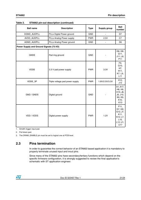
STA662 Pin description<br />
Table 2. STA662 pin-out description (continued)<br />
Ball name Description Type Supply group<br />
DGND_AUDPLL PLLs Digital Power ground GND - D7<br />
AVDD_AUDPLL PLLs Analog Power supply PWR 2.5V C7<br />
AGND_AUDPLL PLLs Analog Power ground GND - D6<br />
Power Supply and Ground Signals (73 I/O)<br />
GNDE Pad ring ground GND -<br />
VDDE 3.3 V pad power supply PWR 3.3V<br />
VDDE_3P Triple voltage pad power supply PWR 1.8V/2.5V/3.3V<br />
GND / GNDS Digital ground GND -<br />
VDD / VDDS Digital power supply PWR 1.2V<br />
1. Smidth trigger input pad.<br />
2. Pull down pad.<br />
3. The DR<strong>AM</strong>_ENABLE pin must be set to logical one at PCB level.<br />
2.3 Pins termination<br />
Ball<br />
number<br />
G6, G8,<br />
G11,<br />
J11, L8,<br />
P11<br />
F9,<br />
G10,<br />
H7,<br />
H11,<br />
K7, L9,<br />
L11<br />
In order to guarantee the correct behavior of an STA662 based application it is mandatory to<br />
properly terminate unused input and inout pins.<br />
Since many of the STA662 pins have secondary/tertiary functions which depend on the<br />
specific firmware configuration, it is strongly suggested to review the final application's<br />
schematic with ST application engineer.<br />
H12,<br />
J12<br />
A1, A17,<br />
H8, H9,<br />
H10, J8,<br />
J9, J10,<br />
K8, K9,<br />
K10,<br />
K13<br />
F11,<br />
G7, G9,<br />
G12, J7,<br />
K11,<br />
K12, L7,<br />
L10,<br />
L12, U1,<br />
U17<br />
Doc ID 023407 Rev 1 21/24