BT151--PHILIPS-

You also want an ePaper? Increase the reach of your titles
YUMPU automatically turns print PDFs into web optimized ePapers that Google loves.
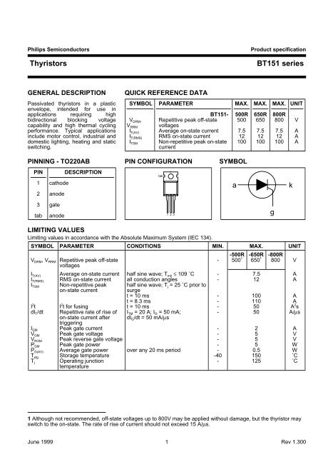
Philips Semiconductors<br />
Thyristors<br />
Product specification<br />
<strong>BT151</strong> series<br />
GENERAL DESCRIPTION<br />
QUICK REFERENCE DATA<br />
Passivated thyristors in a plastic SYMBOL PARAMETER MAX. MAX. MAX. UNIT<br />
envelope, intended for use in<br />
applications requiring high <strong>BT151</strong>- 500R 650R 800R<br />
bidirectional blocking voltage V DRM , Repetitive peak off-state 500 650 800 V<br />
capability and high thermal cycling V RRM voltages<br />
performance. Typical applications I T(AV) Average on-state current 7.5 7.5 7.5 A<br />
include motor control, industrial and I T(RMS) RMS on-state current 12 12 12 A<br />
domestic lighting, heating and static I TSM Non-repetitive peak on-state 100 100 100 A<br />
switching.<br />
current<br />
PINNING - TO220AB PIN CONFIGURATION SYMBOL<br />
PIN DESCRIPTION<br />
1 cathode<br />
2 anode<br />
tab<br />
a<br />
k<br />
3 gate<br />
tab<br />
anode<br />
123<br />
g<br />
LIMITING VALUES<br />
Limiting values in accordance with the Absolute Maximum System (IEC 134).<br />
SYMBOL PARAMETER CONDITIONS MIN. MAX. UNIT<br />
-500R -650R -800R<br />
V DRM , V RRM Repetitive peak off-state<br />
voltages<br />
- 500 1 650 1 800 V<br />
I T(AV) Average on-state current half sine wave; T mb ≤ 109 ˚C - 7.5 A<br />
I T(RMS) RMS on-state current all conduction angles - 12 A<br />
I TSM Non-repetitive peak half sine wave; T j = 25 ˚C prior to<br />
on-state current<br />
surge<br />
t = 10 ms - 100 A<br />
I 2 t I 2 t for fusing<br />
t = 8.3 ms<br />
t = 10 ms<br />
-<br />
-<br />
110<br />
50<br />
A<br />
A 2 s<br />
dI T /dt Repetitive rate of rise of I TM = 20 A; I G = 50 mA; - 50 A/µs<br />
on-state current after<br />
triggering<br />
dI G /dt = 50 mA/µs<br />
I GM Peak gate current - 2 A<br />
V GM Peak gate voltage - 5 V<br />
V RGM Peak reverse gate voltage - 5 V<br />
P GM Peak gate power - 5 W<br />
P G(AV) Average gate power over any 20 ms period - 0.5 W<br />
T stg Storage temperature -40 150 ˚C<br />
T j Operating junction - 125 ˚C<br />
temperature<br />
1 Although not recommended, off-state voltages up to 800V may be applied without damage, but the thyristor may<br />
switch to the on-state. The rate of rise of current should not exceed 15 A/µs.<br />
June 1999 1 Rev 1.300
Philips Semiconductors<br />
Thyristors<br />
Product specification<br />
<strong>BT151</strong> series<br />
THERMAL RESISTANCES<br />
SYMBOL PARAMETER CONDITIONS MIN. TYP. MAX. UNIT<br />
R th j-mb Thermal resistance - - 1.3 K/W<br />
junction to mounting base<br />
R th j-a Thermal resistance in free air - 60 - K/W<br />
junction to ambient<br />
STATIC CHARACTERISTICS<br />
T j = 25 ˚C unless otherwise stated<br />
SYMBOL PARAMETER CONDITIONS MIN. TYP. MAX. UNIT<br />
I GT Gate trigger current V D = 12 V; I T = 0.1 A - 2 15 mA<br />
I L Latching current V D = 12 V; I GT = 0.1 A - 10 40 mA<br />
I H Holding current V D = 12 V; I GT = 0.1 A - 7 20 mA<br />
V T On-state voltage I T = 23 A - 1.4 1.75 V<br />
V GT Gate trigger voltage V D = 12 V; I T = 0.1 A - 0.6 1.5 V<br />
V D = V DRM(max) ; I T = 0.1 A; T j = 125 ˚C 0.25 0.4 - V<br />
I D , I R Off-state leakage current V D = V DRM(max) ; V R = V RRM(max) ; T j = 125 ˚C - 0.1 0.5 mA<br />
DYNAMIC CHARACTERISTICS<br />
T j = 25 ˚C unless otherwise stated<br />
SYMBOL PARAMETER CONDITIONS MIN. TYP. MAX. UNIT<br />
dV D /dt Critical rate of rise of V DM = 67% V DRM(max) ; T j = 125 ˚C;<br />
off-state voltage<br />
exponential waveform;<br />
GK<br />
t gt Gate controlled turn-on I TM = 40 A; V D = V DRM(max) ; I G = 0.1 A; - 2 - µs<br />
Gate open circuit<br />
R = 100 Ω<br />
50<br />
200<br />
130<br />
1000<br />
-<br />
-<br />
V/µs<br />
V/µs<br />
t q<br />
time<br />
dI G /dt = 5 A/µs<br />
Circuit commutated V D = 67% V DRM(max) ; T j = 125 ˚C;<br />
turn-off time<br />
I TM = 20 A; V R = 25 V; dI TM /dt = 30 A/µs;<br />
- 70 - µs<br />
dV D /dt = 50 V/µs; R GK = 100 Ω<br />
June 1999 2 Rev 1.300
Philips Semiconductors<br />
Thyristors<br />
Product specification<br />
<strong>BT151</strong> series<br />
Ptot / W<br />
15<br />
10<br />
conduction<br />
angle<br />
degrees<br />
30<br />
60<br />
90<br />
120<br />
180<br />
form<br />
factor<br />
a<br />
4<br />
2.8<br />
2.2<br />
1.9<br />
1.57<br />
2.8<br />
2.2<br />
Tmb(max) / C<br />
105.5<br />
a = 1.57<br />
1.9<br />
112<br />
ITSM / A<br />
120<br />
100<br />
80<br />
I<br />
ITSM<br />
T<br />
T time<br />
Tj initial = 25 C max<br />
4<br />
60<br />
5<br />
118.5<br />
40<br />
20<br />
0<br />
0 1 2 3 4 5 6 7<br />
125<br />
8<br />
IT(AV) / A<br />
Fig.1. Maximum on-state dissipation, P tot , versus<br />
average on-state current, I T(AV) , where<br />
a = form factor = I T(RMS) / I T(AV) .<br />
0<br />
1 10 100 1000<br />
Number of half cycles at 50Hz<br />
Fig.4. Maximum permissible non-repetitive peak<br />
on-state current I TSM , versus number of cycles, for<br />
sinusoidal currents, f = 50 Hz.<br />
ITSM / A<br />
1000<br />
IT(RMS) / A<br />
25<br />
20<br />
100<br />
dI /dt limit T<br />
15<br />
IT<br />
I TSM<br />
10<br />
T<br />
time<br />
Tj initial = 25 C max<br />
10<br />
10us 100us 1ms 10ms<br />
T / s<br />
Fig.2. Maximum permissible non-repetitive peak<br />
on-state current I TSM , versus pulse width t p , for<br />
sinusoidal currents, t p ≤ 10ms.<br />
5<br />
0<br />
0.01 0.1 1 10<br />
surge duration / s<br />
Fig.5. Maximum permissible repetitive rms on-state<br />
current I T(RMS) , versus surge duration, for sinusoidal<br />
currents, f = 50 Hz; T mb ≤ 109˚C.<br />
IT(RMS) / A<br />
15<br />
<strong>BT151</strong><br />
1.6<br />
VGT(Tj)<br />
VGT(25 C)<br />
109 C<br />
1.4<br />
10<br />
1.2<br />
1<br />
5<br />
0.8<br />
0.6<br />
0<br />
-50 0 50 100 150<br />
Tmb / C<br />
Fig.3. Maximum permissible rms current I T(RMS) ,<br />
versus mounting base temperature T mb .<br />
0.4<br />
-50 0 50 100 150<br />
Tj / C<br />
Fig.6. Normalised gate trigger voltage<br />
V GT (T j )/ V GT (25˚C), versus junction temperature T j .<br />
June 1999 3 Rev 1.300
Philips Semiconductors<br />
Thyristors<br />
Product specification<br />
<strong>BT151</strong> series<br />
3<br />
2.5<br />
2<br />
IGT(Tj)<br />
IGT(25 C)<br />
IT / A<br />
30<br />
Tj = 125 C<br />
Tj = 25 C<br />
25<br />
Vo = 1.06 V<br />
Rs = 0.0304 ohms<br />
20<br />
typ<br />
max<br />
1.5<br />
15<br />
1<br />
10<br />
0.5<br />
5<br />
0<br />
-50 0 50 100 150<br />
Tj / C<br />
Fig.7. Normalised gate trigger current<br />
I GT (T j )/ I GT (25˚C), versus junction temperature T j .<br />
0<br />
0 0.5 1 1.5 2<br />
VT / V<br />
Fig.10. Typical and maximum on-state characteristic.<br />
3<br />
IL(Tj)<br />
IL(25 C)<br />
BT145<br />
Zth j-mb (K/W)<br />
10<br />
2.5<br />
2<br />
1.5<br />
1<br />
0.1<br />
1<br />
0.01<br />
P<br />
D<br />
t p<br />
0.5<br />
t<br />
0<br />
-50 0 50 100 150<br />
Tj / C<br />
Fig.8. Normalised latching current I L (T j )/ I L (25˚C),<br />
versus junction temperature T j .<br />
0.001<br />
10us 0.1ms 1ms 10ms 0.1s 1s 10s<br />
tp / s<br />
Fig.11. Transient thermal impedance Z th j-mb , versus<br />
pulse width t p .<br />
3<br />
IH(Tj)<br />
IH(25 C)<br />
dVD/dt (V/us)<br />
10000<br />
2.5<br />
2<br />
1000<br />
1.5<br />
1<br />
100<br />
RGK = 100 Ohms<br />
gate open circuit<br />
0.5<br />
0<br />
-50 0 50 100 150<br />
Tj / C<br />
Fig.9. Normalised holding current I H (T j )/ I H (25˚C),<br />
versus junction temperature T j .<br />
10<br />
0 50 100 150<br />
Tj / C<br />
Fig.12. Typical, critical rate of rise of off-state voltage,<br />
dV D /dt versus junction temperature T j .<br />
June 1999 4 Rev 1.300
Philips Semiconductors<br />
Thyristors<br />
Product specification<br />
<strong>BT151</strong> series<br />
MECHANICAL DATA<br />
Dimensions in mm<br />
Net Mass: 2 g<br />
4,5<br />
max<br />
10,3<br />
max<br />
3,7<br />
1,3<br />
2,8<br />
5,9<br />
min<br />
15,8<br />
max<br />
3,0 max<br />
not tinned<br />
1,3<br />
max<br />
(2x)<br />
1 2 3<br />
2,54 2,54<br />
3,0<br />
13,5<br />
min<br />
0,9 max (3x)<br />
0,6<br />
2,4<br />
Notes<br />
1. Refer to mounting instructions for SOT78 (TO220) envelopes.<br />
2. Epoxy meets UL94 V0 at 1/8".<br />
Fig.13. SOT78 (TO220AB). pin 2 connected to mounting base.<br />
June 1999 5 Rev 1.300
Philips Semiconductors<br />
Thyristors<br />
Product specification<br />
<strong>BT151</strong> series<br />
DEFINITIONS<br />
Data sheet status<br />
Objective specification This data sheet contains target or goal specifications for product development.<br />
Preliminary specification This data sheet contains preliminary data; supplementary data may be published later.<br />
Product specification This data sheet contains final product specifications.<br />
Limiting values<br />
Limiting values are given in accordance with the Absolute Maximum Rating System (IEC 134). Stress above one<br />
or more of the limiting values may cause permanent damage to the device. These are stress ratings only and<br />
operation of the device at these or at any other conditions above those given in the Characteristics sections of<br />
this specification is not implied. Exposure to limiting values for extended periods may affect device reliability.<br />
Application information<br />
Where application information is given, it is advisory and does not form part of the specification.<br />
© Philips Electronics N.V. 1999<br />
All rights are reserved. Reproduction in whole or in part is prohibited without the prior written consent of the<br />
copyright owner.<br />
The information presented in this document does not form part of any quotation or contract, it is believed to be<br />
accurate and reliable and may be changed without notice. No liability will be accepted by the publisher for any<br />
consequence of its use. Publication thereof does not convey nor imply any license under patent or other<br />
industrial or intellectual property rights.<br />
LIFE SUPPORT APPLICATIONS<br />
These products are not designed for use in life support appliances, devices or systems where malfunction of these<br />
products can be reasonably expected to result in personal injury. Philips customers using or selling these products<br />
for use in such applications do so at their own risk and agree to fully indemnify Philips for any damages resulting<br />
from such improper use or sale.<br />
June 1999 6 Rev 1.300