

Pickering Electronics Catalog Jan17

You also want an ePaper? Increase the reach of your titles
YUMPU automatically turns print PDFs into web optimized ePapers that Google loves.
High Density Vertical<br />
Series 115 switch ratings - The contact ratings for each switch type are shown below:<br />
Switch<br />
No<br />
Switch<br />
form<br />
Switch no.2 is particularly good for switching low currents and/or voltages. It is the ideal switch for A.T.E. systems where cold switching<br />
techniques are often used. Where higher power levels are involved, switch no.1 is more suitable.<br />
Coil data and type numbers<br />
Device<br />
type<br />
1 Form A (energize to make)<br />
General Purpose<br />
Switch No. 1<br />
1 Form A (energize to make)<br />
Low Level Switch No. 2<br />
2 Form A (energize to make)<br />
Low Level Switch No. 2<br />
Power rating<br />
Operating voltages<br />
Coil voltage - nominal Must operate voltage - maximum at 25°C Must release voltage - minimum at 25°C<br />
3 V 2.25 V 0.3 V<br />
5 V 3.75 V 0.5 V<br />
12 V 9.0 V 1.2 V<br />
Type Number<br />
115-1-A-3/1D<br />
115-1-A-5/1D<br />
115-1-A-12/1D<br />
115-1-A-3/2D<br />
115-1-A-5/2D<br />
115-1-A-12/2D<br />
115-2-A-5/1D<br />
115-2-A-5/2D<br />
Coil<br />
(V)<br />
3<br />
5<br />
12<br />
3<br />
5<br />
12<br />
Coil<br />
resistance<br />
250 Ω<br />
500 Ω<br />
1000 Ω<br />
250 Ω<br />
500 Ω<br />
1000 Ω<br />
Max.<br />
contact<br />
resistance<br />
(initial)<br />
Insulation resistance<br />
(minimum)<br />
Switch<br />
to coil<br />
When an internal diode is required, the suffix D is added to the part number as shown in the table.<br />
Environmental specification<br />
Max.<br />
switch<br />
current<br />
5<br />
5<br />
Max.<br />
carry<br />
current<br />
250 Ω<br />
350 Ω<br />
Max.<br />
switching<br />
volts<br />
Life expectancy<br />
ops typical<br />
(see Note 1 below)<br />
Note 3 Capacitance across open switch<br />
The capacitance across the open switch was measured with other connections guarded.<br />
Across<br />
switch<br />
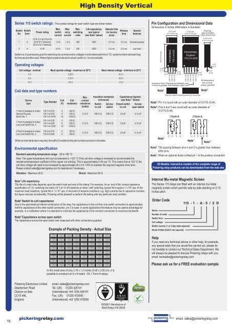
Example of Packing Density - Actual Size<br />
Operate time<br />
inc bounce<br />
(max)<br />
Capacitance (typical)<br />
(see Note 2,3 below)<br />
Closed switch<br />
to coil<br />
Across<br />
open switch<br />
0.12 Ω 10E12 Ω 10E12 Ω 2.9 pF 0.14 pF<br />
0.12 Ω 10E12 Ω 10E12 Ω 2.9 pF 0.14 pF<br />
0.12 Ω 10E12 Ω 10E12 Ω 2.9 pF 0.14 pF<br />
Note 2 Switch to coil capacitance<br />
Due to the asymmetrical internal construction of the relay, the capacitance to the coil from one switch connection is approximately<br />
half the capacitance of the other switch connection, pin 3 is lower. In some applications this feature may be used to advantage for<br />
example, in a multiplexer where it is desirable to minimize the capacitance of the common connection to maximize bandwidth.<br />
In this small area of only 2.16 x 1.2 inches (5.48 x 3.05 cm), it is<br />
possible to construct an 8 x 8 matrix - 64, 1 Form A relays.<br />
Release<br />
time<br />
Special<br />
features<br />
1 A<br />
15 W (3 V & 2 Form A)<br />
20 W (5 V Versions) 1.0 A 1.2 A 200 10E9 0.5 ms 0.2 ms General purpose<br />
20 W (12 V Versions)<br />
2 A 10 W 0.5 A 1.2 A 200 10E9 0.5 ms 0.2 ms Low level<br />
Standard operating temperature range: -20 to +85 °C.<br />
Note: The upper temperature limit can be extended to +125 °C if the coil drive voltage is increased to accommodate the<br />
resistance/temperature coefficient of the copper coil winding. This is approximately 0.4% per °C. This means that at 125 °C the<br />
coil drive voltage will need to be increased by approximately 40 x 0.4 =16% to maintain the required magnetic drive level.<br />
Please contact sales@pickeringrelay.com for assistance if necessary.<br />
Vibration: Maximum 20 G<br />
Shock: Maximum 50 G<br />
Note 1 Life expectancy<br />
The life of a reed relay depends upon the switch load and end of life criteria. For example, for an ‘end of life’ contact resistance<br />
specification of 1 Ω, switching low loads (10 V at 10 mA resistive) or when ‘cold’ switching, typical life is approx 1 x 10 9 ops. At the<br />
maximum load (resistive), typical life is 1 x 10 7 ops. In the event of abusive conditions, e.g. high currents due to capacitive inrushes,<br />
this figure reduces considerably. <strong>Pickering</strong> will be pleased to perform life testing with any particular load condition.<br />
RELAY RELAY RELAY RELAY RELAY RELAY RELAY RELAY<br />
RELAY RELAY RELAY RELAY RELAY RELAY RELAY RELAY<br />
RELAY RELAY RELAY RELAY RELAY RELAY RELAY RELAY<br />
RELAY RELAY RELAY RELAY RELAY RELAY RELAY RELAY<br />
RELAY RELAY RELAY RELAY RELAY RELAY RELAY RELAY<br />
RELAY RELAY RELAY RELAY RELAY RELAY RELAY RELAY<br />
RELAY RELAY RELAY RELAY RELAY RELAY RELAY RELAY<br />
RELAY RELAY RELAY RELAY RELAY RELAY RELAY RELAY<br />
Pin Configuration and Dimensional Data<br />
Dimensions in Inches (Millimeters in brackets)<br />
0.61 (15.5) max.<br />
0.125<br />
(3.17)<br />
Pin 1<br />
3D Models: Interactive models of the complete range of<br />
<strong>Pickering</strong> relay products can be downloaded from the web site.<br />
Internal Mu-metal Magnetic Screen<br />
The Series 115 relays are fitted with an internal mu-metal<br />
magnetic screen which permits side-by-side stacking on 0.15<br />
inches pitch.<br />
Order Code<br />
0.26 (6.60)<br />
0.27 (6.86) max.<br />
PICKERING<br />
115-1-A-5/2D<br />
0.06 (1.52)<br />
0.06 (1.52)<br />
0.06 (1.52)<br />
0.015<br />
(0.38)<br />
Important note: The spacing between pins<br />
4 and 5 is greater than between other pins<br />
Series<br />
Number of reeds<br />
Switch form<br />
Coil voltage<br />
Switch number (1 or 2 See table adjacent)<br />
Diode if fitted (Omit if not required)<br />
0.39 (9.90)<br />
0.40 (10.16) max.<br />
PICKERING<br />
England<br />
115-2-A-5/2D<br />
0.06 (1.52)<br />
0.015<br />
(0.38)<br />
Drawing<br />
approximately<br />
twice actual size<br />
0.145 (3.70)<br />
0.15 (3.81) max.<br />
0.01<br />
(0.25)<br />
All dimensions<br />
are nominal<br />
unless specified<br />
Note 4 Note 5<br />
115 - 1 - A - 5 / 2 D<br />
Help<br />
If you need any technical advice or other help, for example,<br />
any special tests that you would like carried out, please do<br />
not hesitate to contact our Technical Sales Department. We<br />
will always be pleased to discuss <strong>Pickering</strong> relays with you.<br />
email: techsales@pickeringrelay.com<br />
Please ask us for a FREE evaluation sample.<br />
0.06 (1.52)<br />
0.06 (1.52)<br />
0.07 (1.78)<br />
0.06 (1.52)<br />
View from below showing postion of round pins<br />
Note 4 : Pin 3 is round with an outer diameter of 0.0175 (0.44).<br />
Note 5 : Pins 4 and 5 are round with an outer diameter of<br />
0.0175 (0.44).<br />
1 Form A 2 Form A<br />
1+ 2 3 4 1+ 2 3 4 5 6<br />
Note 7 Note 7<br />
Note 6<br />
Note 6 : The spacing between pins 4 and 5 is greater than between<br />
other pins.<br />
Note 7 : When an optional diode is fitted pin 1 is the positive connection.<br />
0.02<br />
(0.5)<br />
<strong>Pickering</strong> <strong>Electronics</strong> Limited<br />
Stephenson Road<br />
Clacton-on-Sea<br />
CO15 4NL<br />
England<br />
email: sales@pickeringrelay.com<br />
Tel. (UK) 01255 428141<br />
(International) +44 1255 428141<br />
Fax. (UK) 01255 475058<br />
(International) +44 1255 475058<br />
ISO9001 Manufacture of<br />
Reed Relays FM 29036<br />
16<br />
pickeringrelay.com<br />
pickering<br />
email: sales@pickeringrelay.com