Lasers in Solar Manufacturing - Coherent
Lasers in Solar Manufacturing - Coherent
Lasers in Solar Manufacturing - Coherent
You also want an ePaper? Increase the reach of your titles
YUMPU automatically turns print PDFs into web optimized ePapers that Google loves.
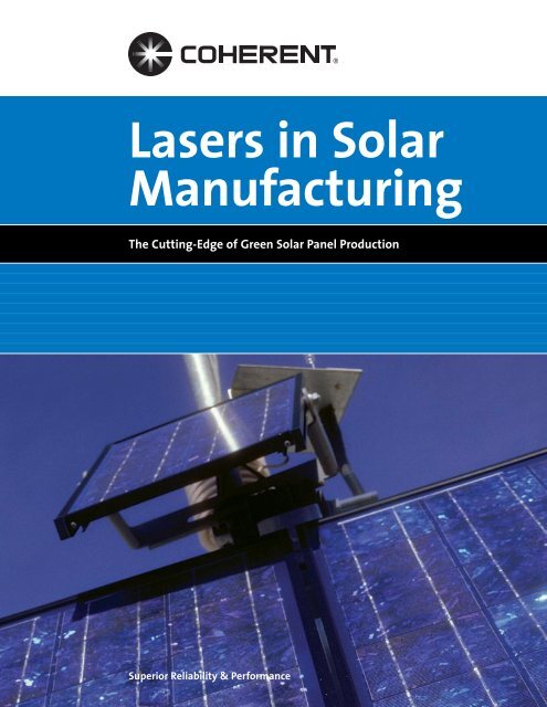
<strong>Lasers</strong> <strong>in</strong> <strong>Solar</strong><br />
Manufactur<strong>in</strong>g<br />
The Cutt<strong>in</strong>g-Edge of Green <strong>Solar</strong> Panel Production<br />
Superior Reliability & Performance
P1 (below) and P3 (right) layer pattern<strong>in</strong>g<br />
<strong>in</strong> a-Si th<strong>in</strong>-film panels<br />
Key Requirements of a Laser Supplier for <strong>Solar</strong> Manufactur<strong>in</strong>g<br />
• Optimized laser sources for solar cell & panel manufactur<strong>in</strong>g<br />
• Turn-key diode-pumped solid-state lasers<br />
• Industrial qualified from semiconductor & flat-panel <strong>in</strong>dustry heritage<br />
• Worldwide service & support network<br />
Talisker and Palad<strong>in</strong> lasers offer picosecond pulses <strong>in</strong> the IR, Green, and UV<br />
• Range of wavelengths from IR to UV for different material absorptions<br />
• High peak powers for scrib<strong>in</strong>g, ablat<strong>in</strong>g, & melt<strong>in</strong>g applications<br />
• High average powers for high production throughput<br />
• High quality beam parameters for narrow l<strong>in</strong>es & feature sizes<br />
• Optimized models for all c-Si & th<strong>in</strong>-film applications<br />
• Enabl<strong>in</strong>g novel cell concepts <strong>in</strong> R&D and pilot-l<strong>in</strong>es
<strong>Coherent</strong> <strong>Lasers</strong> <strong>in</strong> <strong>Solar</strong> Cell Applications<br />
Crystall<strong>in</strong>e-Silicon<br />
Edge Isolation •<br />
Laser Grooved Buried Contacts •<br />
Textur<strong>in</strong>g • • •<br />
Selective Ablation • •<br />
Wrap-Through • •<br />
AVIA LAMBDA SX Talisker Palad<strong>in</strong> PRISMA FAP System MATRIX<br />
Dopant Diffusion •<br />
Laser Fired Contacts •<br />
Interconnection •<br />
Th<strong>in</strong> Film<br />
a:Si Pattern<strong>in</strong>g • • •<br />
CIGS Patter<strong>in</strong>g • • •<br />
CdTe Pattern<strong>in</strong>g • •<br />
<strong>Solar</strong> Cell Applications<br />
• c-Si Edge Isolation<br />
• c-Si Laser Fired Contacts<br />
• c-Si Wafer Mark<strong>in</strong>g<br />
• c-Si Laser Grooved Buried Contacts<br />
• c-Si Selective Dielectric Removal<br />
• c-Si Laser Dop<strong>in</strong>g<br />
• c-Si Wrap-Through<br />
• c-Si Textur<strong>in</strong>g<br />
• c-Si S<strong>in</strong>gulation<br />
• a-Si & a-Si/mc-Si Pattern<strong>in</strong>g<br />
• CIGS Pattern<strong>in</strong>g<br />
• CdTe Pattern<strong>in</strong>g<br />
• Border Deletion<br />
• Glass Cutt<strong>in</strong>g<br />
<strong>Lasers</strong> as a solution to decreas<strong>in</strong>g<br />
manufactur<strong>in</strong>g costs and <strong>in</strong>creas<strong>in</strong>g<br />
product efficiency<br />
As <strong>in</strong> most manufactur<strong>in</strong>g processes, controll<strong>in</strong>g<br />
the production costs is the first step<br />
toward profitability. Although <strong>in</strong>vestments <strong>in</strong><br />
research and development rema<strong>in</strong> critical, <strong>in</strong><br />
the solar energy bus<strong>in</strong>ess, how to make the<br />
product is less of a concern than how to make<br />
them quickly <strong>in</strong> volume production at low<br />
cost and with a higher degree of efficiency.<br />
As the efficiency of each cell produced<br />
<strong>in</strong>creases, and the cost of produc<strong>in</strong>g these<br />
cells decreases, the closer solar energy comes<br />
to match<strong>in</strong>g the cost of exist<strong>in</strong>g energy<br />
sources. At that po<strong>in</strong>t – when a kilowatt of<br />
solar power costs the same or less than traditional<br />
energy sources – the challenge will be<br />
how quickly the solar <strong>in</strong>dustry can grow rather<br />
than how successful it is projected to be.<br />
With this “grid parity” condition be<strong>in</strong>g<br />
the <strong>in</strong>itial goal of the solar <strong>in</strong>dustry, lasers<br />
are already one of the most important<br />
components <strong>in</strong> reach<strong>in</strong>g that level.<br />
Laser edge isolation of c-Si cell<br />
<strong>Coherent</strong> lasers <strong>in</strong> solar<br />
manufactur<strong>in</strong>g processes<br />
<strong>Coherent</strong> lasers form an <strong>in</strong>tegral part of<br />
the solar <strong>in</strong>dustry’s roadmap today. Here,<br />
they <strong>in</strong>crease the yield (or throughput)<br />
levels, improve the efficiency of solar cells,<br />
allow non-contact process<strong>in</strong>g on larger and<br />
th<strong>in</strong>ner wafers, and enable the implementation<br />
of low cost-of-ownership production<br />
l<strong>in</strong>e equipment.<br />
There are two compet<strong>in</strong>g types of solar<br />
cells produced today <strong>in</strong> high volume –<br />
silicon wafers and th<strong>in</strong>-film substrates.<br />
In both silicon wafer manufactur<strong>in</strong>g –<br />
whose end products are crystall<strong>in</strong>e-silicon<br />
(c-Si) solar cells – or <strong>in</strong> the production<br />
of th<strong>in</strong>-film solar panels <strong>in</strong>corporat<strong>in</strong>g<br />
materials such as amorphous silicon (a-Si),<br />
cadmium telluride, or copper <strong>in</strong>dium<br />
gallium selenide, <strong>Coherent</strong> lasers create<br />
precise and repeatable pulses of energy<br />
to scribe, ablate or melt specific materialgroups<br />
used <strong>in</strong> the different manufactur<strong>in</strong>g<br />
processes.
By perform<strong>in</strong>g the necessary material<br />
removal or scrib<strong>in</strong>g of surfaces by a<br />
non-contact method, lasers produce the<br />
highest efficiencies <strong>in</strong> the <strong>in</strong>dividual cells,<br />
while also reduc<strong>in</strong>g micro-crack<strong>in</strong>g, and<br />
<strong>in</strong>creas<strong>in</strong>g the overall cell efficiencies.<br />
<strong>Coherent</strong> lasers also produce results more<br />
quickly than any other technology, as well<br />
as faster and more efficiently than any<br />
other type or brand of laser.<br />
Crystall<strong>in</strong>e-silicon (c-Si) cell<br />
manufactur<strong>in</strong>g<br />
In the crystall<strong>in</strong>e-silicon cell production<br />
method, th<strong>in</strong> silicon wafers are transformed<br />
<strong>in</strong>to functional solar cells.<br />
<strong>Coherent</strong>’s pulsed diode-pumped solid-state<br />
lasers, operat<strong>in</strong>g <strong>in</strong> the <strong>in</strong>frared, green or<br />
ultraviolet spectral regions, are rout<strong>in</strong>ely<br />
<strong>in</strong>tegrated with<strong>in</strong> the most efficient and<br />
productive tools to enable novel high-efficiency<br />
concepts to be realized. This <strong>in</strong>cludes a<br />
range of front and rear surface processes,<br />
<strong>in</strong> addition to through via hole drill<strong>in</strong>g.<br />
c-Si edge isolation method<br />
How our AVIA lasers elim<strong>in</strong>ate<br />
the dop<strong>in</strong>g “pathways” problem<br />
With<strong>in</strong> each solar cell the p-n junction<br />
that creates the electrical current requires<br />
that the front of the positive-conduct<strong>in</strong>g<br />
boron-doped silicon wafer be exposed to a<br />
phosphorous gas <strong>in</strong> order to dope an n-type<br />
conduct<strong>in</strong>g film on the top surface of the<br />
cell. However, this dop<strong>in</strong>g process has a<br />
detrimental effect on the cell performance;<br />
it coats not only the front surface of the<br />
wafer, but the sides, as well. This side coat<strong>in</strong>g<br />
creates a shunt path between the front and<br />
rear surfaces, which prevents the cell from<br />
operat<strong>in</strong>g efficiently.<br />
To fix this problem, our AVIA lasers –<br />
operat<strong>in</strong>g <strong>in</strong> the green or ultraviolet wavelength<br />
regions at 532 nm or 355 nm – scribe<br />
a cont<strong>in</strong>uous groove completely through the<br />
n-type layer of the p-n junction and around<br />
the entire perimeter of the front surface.<br />
This scribed groove isolates the front and<br />
the back surfaces of the cell, elim<strong>in</strong>at<strong>in</strong>g the<br />
shunt path and <strong>in</strong>creas<strong>in</strong>g cell efficiency.<br />
AVIA and MATRIX lasers offer nanosecond pulses <strong>in</strong> the IR, Green, and UV<br />
Laser grooved buried contact on a c-Si cell<br />
By us<strong>in</strong>g a laser, this non-contact process is<br />
faster and cleaner than other methods which<br />
<strong>in</strong>volve hazardous chemicals and waste produce.<br />
The high power – up to 38W – of our AVIA<br />
lasers allow process<strong>in</strong>g of greater than<br />
3,000 wafers per hour. Due to the strong<br />
absorption of silicon <strong>in</strong> the visible and<br />
ultraviolet spectral regions, the shortwavelength<br />
output from AVIA lasers reduce<br />
any micro-crack<strong>in</strong>g with<strong>in</strong> the silicon wafer:<br />
a problem often reported with lasers which<br />
operate <strong>in</strong> the <strong>in</strong>frared. High power and<br />
short wavelength output of AVIA lasers<br />
comb<strong>in</strong>e to allow both faster production<br />
l<strong>in</strong>e capacities and higher material yields.<br />
Th<strong>in</strong>-film solar panel manufactur<strong>in</strong>g<br />
In the th<strong>in</strong>-film solar manufactur<strong>in</strong>g process,<br />
our nanosecond diode-pumped solid-state<br />
lasers are used typically at the cell isolation<br />
and <strong>in</strong>terconnection stage, commonly<br />
referred to as “pattern<strong>in</strong>g”. This is a 3-step<br />
process <strong>in</strong> which our lasers perform material<br />
removal after each layer deposition stage.
Average Power Level (W)<br />
50<br />
40<br />
30<br />
20<br />
10<br />
0<br />
1998<br />
AVIA-532<br />
AVIA-355<br />
2000 2002 2004 2006 2008<br />
Year of New Power Level Launch<br />
In the case of amorphous silicon panels,<br />
the first pattern<strong>in</strong>g stage (P1) <strong>in</strong>volves<br />
material ablation of the front-contact<br />
transparent conduct<strong>in</strong>g oxide (TCO) layer.<br />
Here, an <strong>in</strong>frared laser operat<strong>in</strong>g at 1064 nm<br />
provides an ideal match <strong>in</strong> terms of output<br />
power, repetition rate and material absorption.<br />
Next, <strong>in</strong> the P2 step, a laser emitt<strong>in</strong>g <strong>in</strong><br />
the green region at 532 nm creates a pattern<br />
on the amorphous silicon absorber layer.<br />
Lastly, follow<strong>in</strong>g the same process as used at<br />
the P2 stage, a 532 nm laser is aga<strong>in</strong> used to<br />
pattern the back-contact layer of the cell –<br />
the P3 stage.<br />
PRISMA diode-pumped solid-state lasers are<br />
ideal for th<strong>in</strong>-film panel production because<br />
they provide excellent pulse-to-pulse stability,<br />
accurate beam position<strong>in</strong>g on the panels, and<br />
a comb<strong>in</strong>ation of short pulse-width and high<br />
repetition rates greater than 100 kilohertz.<br />
These unique characteristics of our highperformance<br />
<strong>in</strong>frared and green lasers comb<strong>in</strong>e<br />
to produce the demand<strong>in</strong>g performance<br />
required <strong>in</strong> large solar panel manufactur<strong>in</strong>g.<br />
<strong>Solar</strong> Industry roadmap<br />
trends for crystall<strong>in</strong>e-silicon<br />
production<br />
Current ‘Typical’ 5-Year Trends<br />
Cell Efficiency 14 to 18% Increase by 2 to 3%<br />
Wafer Size 125 or 156 mm Move to 210 mm<br />
Wafer Thickness ~220 µm Transition to sub-200 µm<br />
‘Green’ Production Equipment Varies per production l<strong>in</strong>e Cleaner production tools<br />
Yield Levels 85 to 90% Increase to >95%<br />
Th<strong>in</strong>-film pattern<strong>in</strong>g process on a-Si panels<br />
Future growth and <strong>in</strong>creas<strong>in</strong>g benefits<br />
of us<strong>in</strong>g lasers <strong>in</strong> the manufacture of<br />
solar cells and panels<br />
The use of lasers <strong>in</strong> the grow<strong>in</strong>g solar<br />
manufactur<strong>in</strong>g market will become more<br />
important as we move <strong>in</strong>to the future.<br />
With th<strong>in</strong>ner wafers below 200 microns <strong>in</strong><br />
thickness be<strong>in</strong>g implemented over the next<br />
few years, new demands are be<strong>in</strong>g placed<br />
on the type of equipment used with<strong>in</strong> the<br />
manufactur<strong>in</strong>g process. At the same time,<br />
there is a requirement to <strong>in</strong>crease production<br />
yield levels to microelectronics <strong>in</strong>dustry<br />
standards. To address these roadmap<br />
objectives, the "non-contact" nature of laser<br />
systems allows process<strong>in</strong>g on brittle wafers<br />
while m<strong>in</strong>imiz<strong>in</strong>g breakage rates associated<br />
with more traditional technology types.<br />
In addition, solar cell manufacturers are<br />
<strong>in</strong>creas<strong>in</strong>gly under pressure to utilize<br />
production equipment which itself provides<br />
very low 'global warm<strong>in</strong>g potential'. Here,<br />
an ideal - or 'green' - manufactur<strong>in</strong>g process<br />
uses laser equipment to m<strong>in</strong>imize both<br />
water consumption and hazardous<br />
chemical waste. <strong>Coherent</strong>’s diode-pumped<br />
solid-state lasers are ideal equipment<br />
types, with turn-key operation, s<strong>in</strong>glephase<br />
electrical <strong>in</strong>put, and very long<br />
component lifetimes.<br />
Through availability of <strong>in</strong>dustry-qualified<br />
diode-pumped solid-state lasers operat<strong>in</strong>g<br />
at high power from the <strong>in</strong>frared to<br />
ultraviolet spectral regions, and with<br />
the choice of both nanosecond and<br />
picosecond pulse-width operation,<br />
<strong>Coherent</strong>’s lasers are poised to play an<br />
<strong>in</strong>creas<strong>in</strong>gly important role with solar<br />
manufactur<strong>in</strong>g worldwide. Benefit<strong>in</strong>g<br />
from our lasers’ alignment historically<br />
with<strong>in</strong> complementary semiconductor<br />
and displays technology roadmaps, and<br />
utiliz<strong>in</strong>g our exist<strong>in</strong>g worldwide service<br />
and support network, <strong>Coherent</strong> is<br />
uniquely placed to drive high laser<br />
adoption with key technical benefits<br />
for the solar <strong>in</strong>dustry.
Pr<strong>in</strong>ted <strong>in</strong> the U.S.A. MC-037-08-0M1008<br />
Copyright © 2008 <strong>Coherent</strong>, Inc.<br />
<strong>Coherent</strong> as your partner.<br />
To compete and succeed <strong>in</strong> today’s fast-paced research and manufactur<strong>in</strong>g environments, you need<br />
a laser partner who understands your needs. A partner who can provide a wide range of technology<br />
solutions, and the support that goes with them.<br />
S<strong>in</strong>ce 1966, <strong>Coherent</strong> has been help<strong>in</strong>g customers by provid<strong>in</strong>g complete laser-based solutions for<br />
a wide range of commercial and scientific applications.<br />
With a heritage of <strong>in</strong>novation and an uncompromis<strong>in</strong>g position on quality, <strong>Coherent</strong> is the most<br />
forward-th<strong>in</strong>k<strong>in</strong>g and diversified manufacturer of solid-state, gas, excimer and semiconductor lasers<br />
<strong>in</strong> the <strong>in</strong>dustry.<br />
For more <strong>in</strong>formation, visit us on the Web at www.<strong>Coherent</strong>.com. Or call 800-527-3786.<br />
<strong>Coherent</strong>, Inc.<br />
5100 Patrick Henry Drive<br />
Santa Clara, CA 95054<br />
phone (800) 527-3786<br />
(408) 764-4983<br />
fax (800) 362-1170<br />
(408) 988-6838<br />
e-mail tech.sales@<strong>Coherent</strong>.com<br />
www.<strong>Coherent</strong>.com<br />
Benelux +31 (30) 280 6060<br />
Ch<strong>in</strong>a +86 (10) 6280 0209<br />
France +33 (0)1 6985 5145<br />
Germany +49 (6071) 968 333<br />
Italy +39 (02) 34 530 214<br />
Japan +81 (3) 5635 8700<br />
Korea +82 (2) 460 7900<br />
UK +44 (1353) 658 833<br />
<strong>Coherent</strong>’s scientific and <strong>in</strong>dustrial lasers are certified to comply with the Federal<br />
Regulations (21 CFR Subchapter J) as adm<strong>in</strong>istered by the Center for Devices and<br />
Radiological Health on all systems ordered for shipment after August 2, 1976.<br />
INVISIBLE LASER RADIATION.<br />
AVOID EYE OR SKIN EXPOSURE TO<br />
DIRECT OR SCATTERED RADIATION.<br />
CLASS IV LASER RADIATION PRODUCT<br />
PER EN60825-1 (A2:2001)<br />
Q-SWITCHED LASER<br />
PULSE LENGTH: 10 to 150 ns<br />
MAX. OUTPUT AT 266/355 nm<br />
50 kW PEAK, 30W AVERAGE<br />
VISIBLE AND INVISIBLE LASER RADIATION.<br />
AVOID EYE OR SKIN EXPOSURE TO DIRECT<br />
OR SCATTERED RADIATION. CLASS 4<br />
LASER PRODUCT PER IEC 60825-1:2001<br />
λ MAX. POWER MAX. PULSE<br />
1.04 to 1.07 µm<br />
0.79 to 0.82 µm<br />
0.52 to 0.55 µm<br />
0.35 to 0.36 µm<br />
20W<br />
70W<br />
10W<br />
5W<br />
4 mJ/5 nsec<br />
–<br />
2 mJ/5 nsec<br />
1 mJ/4 nsec<br />
INVISIBLE LASER RADIATION.<br />
AVOID EYE OR SKIN EXPOSURE TO<br />
DIRECT OR SCATTERED RADIATION.<br />
CLASS IV LASER RADIATION PRODUCT<br />
PER EN60825-1 (A2:2001)<br />
ENERGY PER PULSE: 250 µJ at 200 kHz<br />
EMITTED WAVELENGTH: 1064, 532 and 355 nm<br />
ISO 9001:2000 Registered


