

Chapter 4 Properties of nanomaterials

Create successful ePaper yourself
Turn your PDF publications into a flip-book with our unique Google optimized e-Paper software.
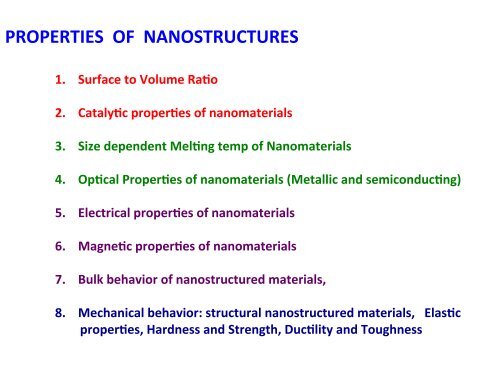
PROPERTIES OF NANOSTRUCTURES<br />
1. Surface to Volume Ra;o<br />
2. Cataly;c proper;es <strong>of</strong> <strong>nanomaterials</strong><br />
3. Size dependent Mel;ng temp <strong>of</strong> Nanomaterials<br />
4. Op;cal Proper;es <strong>of</strong> <strong>nanomaterials</strong> (Metallic and semiconduc;ng)<br />
5. Electrical proper;es <strong>of</strong> <strong>nanomaterials</strong><br />
6. Magne;c proper;es <strong>of</strong> <strong>nanomaterials</strong><br />
7. Bulk behavior <strong>of</strong> nanostructured materials,<br />
8. Mechanical behavior: structural nanostructured materials, Elas;c<br />
proper;es, Hardness and Strength, Duc;lity and Toughness
Size increases the surface<br />
atoms and surface energy<br />
Par;cle size, surface area and<br />
surface energy <strong>of</strong> CaCO 3 .xi (the<br />
surface energy <strong>of</strong> bulk CaCO 3<br />
(calcite) is 0.23 Jm -2 .)
Surface to bulk atom ra;o
Catalysis<br />
Catalysis is the change in rate <strong>of</strong> a chemical reac;on due to the par;cipa;on <strong>of</strong> a<br />
substance called a catalyst.<br />
Unlike other reagents that par;cipate in the chemical reac;on, a catalyst is not<br />
consumed by the reac;on itself.<br />
A catalyst may par;cipate in mul;ple chemical transforma;ons.<br />
Catalysts that speed the reac;on are called posi;ve catalysts.<br />
Substances that interact with catalysts to slow the reac;on are called inhibitors (or<br />
nega;ve catalysts).<br />
Substances that increase the ac;vity <strong>of</strong> catalysts are called promoters, and<br />
substances that deac;vate catalysts are called cataly;c poisons.
Increasing the surface area <strong>of</strong> the solid increases the chances <strong>of</strong> collision taking<br />
place. Imagine a reac;on between magnesium metal and a dilute acid like<br />
hydrochloric acid. The reac;on involves collision between magnesium atoms and<br />
hydrogen ions.
Size-dependent mel;ng <strong>of</strong> low-dimensional systems<br />
Empirical rela;ons are established between the cohesive energy, surface tension,<br />
and mel;ng temperature <strong>of</strong> different bulk solids. An expression for the sizedependent<br />
mel;ng for low-dimensional systems is derived on the basis <strong>of</strong> an<br />
analogy with the liquid-drop model and these empirical rela;ons, and compared<br />
with other theore;cal models as well as the available experimental data in the<br />
literature.
Size-dependent mel;ng <strong>of</strong> nanopar;cles<br />
T mb = bulk mel;ng temperature<br />
T m = mel;ng temperature <strong>of</strong> the nanopar;cles<br />
ν 0 is the volume <strong>of</strong> an atom, and ϒ is the coefficient <strong>of</strong> surface energy <strong>of</strong><br />
the material<br />
Β= Es;mated for different elements<br />
Mel;ng temperature ( T m / T mb ) depends on the inverse <strong>of</strong> the par;cle diameter d.
Mel;ng <strong>of</strong> different-shaped nanopar;cles
Mel;ng <strong>of</strong> thin films<br />
(ld)
General expression <strong>of</strong> Tm for low-dimensional systems
Size and shape dependent lajce parameters <strong>of</strong> metallic<br />
nanopar;cles<br />
It is predicted that the lajce parameters <strong>of</strong> nanopar;cles in several nanometers decrease<br />
with decreasing <strong>of</strong> the par;cle size and the par;cle shape can lead to 10% <strong>of</strong> the total lajce<br />
varia;on<br />
= (a p -a)/a<br />
Where a p and a are the lajce parameters <strong>of</strong> the nanopar;cle and the corresponding bulk<br />
material.<br />
where D (= 2R) is the diameter <strong>of</strong> the nanopar;cle, and K = α 1/2 G/ϒ .<br />
α is a factor to modify the shape difference between the spherical and the non-spherical<br />
nanopar;cles . For spherical nanopar;cle, α= 1, and for non-spherical nanopar;cle, α > 1.<br />
ϒ is the surface energy per unit area at the temperature T (0 ≤ T < Tm, Tm is the mel;ng<br />
temperature <strong>of</strong> metals) and G is the shear module .<br />
Generally, both <strong>of</strong> the shear module and the surface energy are posi;ve; therefore, the lajce<br />
parameter <strong>of</strong> the metallic nanopar;cles will decrease with decreasing <strong>of</strong> the par;cle size.<br />
Equa;on is the basic rela;on for the size and shape dependent lajce parameters <strong>of</strong> metallic<br />
nanopar;cles.
SHAPE DEPENDENCY<br />
Apparently, the shape factor<br />
approaches 1 with increasing the<br />
quan;ty <strong>of</strong> planes. Therefore, the<br />
values <strong>of</strong> regular polyhedral shapes<br />
range from 1 to 1.49.<br />
For disk-like nanopar;cles, the<br />
value <strong>of</strong> shape factor depends on<br />
the ra;o <strong>of</strong> height to radius.<br />
Varia;on <strong>of</strong> the rela;ve<br />
parameter <strong>of</strong> Pd<br />
nanopar;cles as a func;on <strong>of</strong><br />
shape factor.
SIZE<br />
DEPENDENCY<br />
Discussion:<br />
(1) The lajce parameter varia;on depends on the par;cle size and the par;cle shape, and the<br />
varia;on decreases with increasing the shape factor;<br />
(2) The smaller the par;cle size is, the stronger the dependence <strong>of</strong> lajce parameter to the<br />
par;cle shape is;<br />
(3) Both the par;cle shape and the par;cle size can affect the lajce parameter <strong>of</strong><br />
nanopar;cles, but the par;cle size is the main factor, and the par;cle shape is secondary<br />
factor. In generally, the par;cle shape will contribute about 10% to the total lajce varia;on.<br />
In other words, if we ignore the par;cle shape effect when we calculate the lajce parameters<br />
<strong>of</strong> metallic nanopar;cles, the rela;ve error in the final value resul;ng from the par;cle shape<br />
effect may reach 10%.
OPTICAL PROPERTIES OF METAL NANOPARTICLES
The light absorp;on in metal nanopar;cles originates from an interes;ng<br />
phenomenon called localized surface plasmon resonance. According to the Drude–<br />
Lorentz model, the atoms in metals exist in a plasma state, having a core <strong>of</strong><br />
posi;vely charged nuclei surrounded by a pool <strong>of</strong> nega;vely charged electrons and<br />
hence named as ‘plasma electrons’.<br />
In the presence <strong>of</strong> an electromagne;c radia;on, the electric vector displaces the free<br />
electrons and the columbic electrosta;c atrac;on <strong>of</strong> the nuclei will restore the<br />
electrons to the original posi;on.<br />
As a result <strong>of</strong> the oscilla;ng nature <strong>of</strong> the electric field <strong>of</strong> light, the electron cloud<br />
coherently oscillates over the surface with a resonance frequency ‘ωp’. When the<br />
frequency <strong>of</strong> this oscilla;on matches with that <strong>of</strong> incident radia;on, a resonance<br />
condi;on is established which results in the intense absorp;on, oven termed as<br />
‘surface plasmon (SP) absorp;on’.
Op;cal absorp;on proper;es <strong>of</strong> metal nanopar;cles :<br />
The surface Plasmon Resonance<br />
The Mie theory
Op;cal proper;es <strong>of</strong> metal nanopar;cles<br />
par;cle size,<br />
shape,<br />
composi;on,<br />
and the local dielectric environment.
1- Size<br />
The op;cal proper;es <strong>of</strong> large and small nanopar;cles are markedly different.<br />
Kreibig and Vollmer define two types <strong>of</strong> size effects: extrinsic and intrinsic . The<br />
threshold for the two regimes occurs for diameters <strong>of</strong> around 10 nm in the case <strong>of</strong><br />
Au nanopar;cles.<br />
The op;cal proper;es <strong>of</strong> nanopar;cles with diameters above the threshold are<br />
dominated by extrinsic effects, which are related to the diameter and the bulk<br />
dielectric func;on <strong>of</strong> the metal. A red-shiving and broadening <strong>of</strong> the resonance peak<br />
is seen for increasing radius, due to retarda;on effects.<br />
For nanopar;cles with diameters below the threshold several special considera;ons<br />
must be made due to intrinsic effects. This size range is clearly within the quasi-sta;c<br />
regime, and so electrodynamics effects such as retarda;on do not play a role in the<br />
op;cal proper;es. However, surface scatering <strong>of</strong> electrons occurs due to the<br />
par;cle dimensions being smaller than the mean free path, leading to damping <strong>of</strong><br />
the plasmon oscilla;on and a resul;ng atenua;on and broadening <strong>of</strong> the resonance<br />
peak.
2- Shape<br />
Haes et al. elegantly demonstrated the importance <strong>of</strong> par;cle shape by<br />
simula;ng the op;cal spectra <strong>of</strong> various Ag nanopar;cle types with constant<br />
volume. The largest difference occurs between the sphere and pyramid, with a ~200<br />
nm shiv in peak wavelength posi;on. The peak posi;on shiv correlates well with an<br />
increase in the number <strong>of</strong> sharp ;ps or edges as the shape is changed from sphere to<br />
pyramid. Plots <strong>of</strong> |E|2 intensity in the same paper show that the near-field intensity<br />
is strongly confined at sharp features, which results in the red-shiving <strong>of</strong> the far-field<br />
response.
3- Dielectric environment<br />
The op;cal proper;es <strong>of</strong> metal nanopar;cles are strongly sensi;ve to the surrounding dielectric environment,<br />
which is useful for tuning their op;cal proper;es or for biosensing.<br />
In general, an increase <strong>of</strong> refrac;ve index <strong>of</strong> medium surrounding a nanopar;cle results in a red-shiv <strong>of</strong> the LSP<br />
peak.<br />
McFarland and VanDuyne studied the scatering spectra <strong>of</strong> single Ag nanopar;cles as a func;on <strong>of</strong> the<br />
surrounding refrac;ve index . A linear fit between peak posi4on and refrac4ve index <strong>of</strong> a surrounding solvent<br />
was demonstrated (Fig. 2.22).<br />
A thin oxide layer forms on the surfaces <strong>of</strong> Ag, Cu and Al form when these metals are exposed to air.<br />
Langhammer et al. considered the case <strong>of</strong> the self-limi4ng oxide that forms on Al, which was es4mated to be 3<br />
nm thick [136]. This oxide growth has two effects on Al nanopar4cles: (1) the core Al par4cle is reduced in size<br />
during the oxide growth, (2) the local dielectric environment is changed by the outer alumina shell. SVM<br />
simula4ons showed that the change in dielectric environment has the strongest effect on the op4cal proper4es <strong>of</strong><br />
the nanopar4cle, and gives rise to a moderate red-shiQ for large par4cles, and a strong red-shiQ for small<br />
par4cles.
4- Intrapar;cle coupling<br />
In the core-shell nanopar;cle, the inner and outer surfaces <strong>of</strong> the shell support different<br />
resonances. Coupling between the two surfaces leads to an altera;on <strong>of</strong> the overall op;cal<br />
response <strong>of</strong> the nanopar;cle. Prodan et al. developed a hybridiza4on model that can explain<br />
the interac4on between elementary plasmons supported by complex nanopar4cles . For<br />
example, the op4cal response <strong>of</strong> a core-shell nanopar4cle can be considered as the<br />
hybridiza4on <strong>of</strong> a shell plasmon and a cavity plasmon. The strength <strong>of</strong> the interac4on is<br />
controlled by the shell thickness. The op4cal proper4es <strong>of</strong> core-shell nanopar4cles can be<br />
tuned by modifying the core material, core diameter, shell material and shell thickness.<br />
Increasing the refrac4ve index or diameter <strong>of</strong> the core leads to a red-shiQ <strong>of</strong> the resonance.<br />
Decreasing the shell thickness also results in a resonance red-shiQ, which is par4cularly<br />
drama4c for very thin shells.<br />
Standard Mie theory models for core-shell par4cles do not include the effect <strong>of</strong> surface<br />
scaTering, which can be important for thin shells.<br />
Moroz developed an extension to Mie theory to model the effects <strong>of</strong> surface scaTering in coreshell<br />
nanopar4cles. The effect is the same as for very small solid spheres, i.e. damping that<br />
leads to aTenua4on and broadening <strong>of</strong> the peak.
5- Interpar;cle coupling<br />
Systems composed <strong>of</strong> mul;ple par;cles may exhibit op;cal proper;es different than that <strong>of</strong> an isolated<br />
par;cle, even if each par;cle in the group is iden;cal. In the near-field, evanescent fields <strong>of</strong> proximate<br />
nanopar;cles can interact. At larger distances nanopar;cles interact in the far-field through their<br />
scatered fields, which is par;cularly relevant for periodic arrays. Jensen et al. inves;gated near-field<br />
coupling between two iden;cal Ag nanospheres using DDA simula;ons (Fig 2.23). For a par;cle radius <strong>of</strong><br />
30 nm, an interpar;cle spacing <strong>of</strong> 30 nm results in a 10 nm red-shiv <strong>of</strong> the resonance peak. For much<br />
smaller spacing the effect is much more drama;c, resul;ng in 100 nm and 125 nm red-shivs for a spacing<br />
<strong>of</strong> 4 nm and 2 nm respec;vely.<br />
Closely-spaced nanopar;cle pairs exhibit strong polariza;on sensi;vity, as coupling effects are much<br />
weaker for incident light polarized perpendicular to the par;cle pair axis. Complete transfer <strong>of</strong> energy<br />
from one nanopar;cle can occur via dipole-dipole interac;on, leading to the idea <strong>of</strong> sub-wavelength<br />
waveguides based on linear chains <strong>of</strong> metal nanopar;cles. The principle interest in coupled metal<br />
nanopar;cle dimers is the intense electric field enhancement observed in the gap between the par;cles,<br />
which is far larger than those obtained around isolated par;cles. These are found to be strongly related to<br />
the interpar;cle separa;on, with smaller distances producing larger field enhancement.<br />
Par;cles arranged in a periodic patern will scater photons coherently, leading to a change in the<br />
observed far-field scatering spectrum due to interac;on between scatered photons. Periodic<br />
arrangements <strong>of</strong> nanopar;cles form a diffrac;on gra;ng, and coupling <strong>of</strong> LSPs to evanescent or radia;ng<br />
gra;ng modes alters the ex;nc;on spectrum from that <strong>of</strong> isolated nanopar;cles. Essen;ally the<br />
diffrac;on gra;ng imposes restric;ons on the angular distribu;on <strong>of</strong> scatering, and so inhibits or<br />
strengthens scatering at given wavelength. Therefore the op;cal proper;es <strong>of</strong> a periodic array <strong>of</strong><br />
nanopar;cles depend on the gra;ng period in addi;on to the proper;es <strong>of</strong> the individual nanopar;cles.
Summary <strong>of</strong> the op;cal proper;es <strong>of</strong> metal nanopar;cles<br />
The op;cal proper;es <strong>of</strong> metal nanopar;cles are a strong func;on <strong>of</strong> the par;cle composi;on, size,<br />
shape, dielectric environment and the orienta;on and proximity <strong>of</strong> par;cles with respect to each other.<br />
Increasing the size <strong>of</strong> a par;cle results in a red-shiv and broadening <strong>of</strong> the peak posi;on, and an<br />
increase in the ra;o <strong>of</strong> scatering to absorp;on. Large par;cles also support higher- order modes, which<br />
occur at progressively shorter wavelengths, and have a larger absorp;on to scatering ra;o than the<br />
corresponding dipolar peak.<br />
Near-field coupling between nanopar;cles results in a red-shiv, but is only relevant for interpar;cle<br />
spacing <strong>of</strong> the order <strong>of</strong> the par;cle diameter or less. Waveguide-mediated interpar;cle coupling is only<br />
relevant for periodic arrangements <strong>of</strong> par;cles situated on slab waveguides, and results in the<br />
appearance <strong>of</strong> fringes in the ex;nc;on spectrum.<br />
Increasing the refrac;ve index <strong>of</strong> a homogenous medium surrounding a par;cle results in a linear redshiv<br />
<strong>of</strong> ex;nc;on peak posi;on. Inhomogeneous mediums such as substrates and mul;layers can result<br />
in the excita;on <strong>of</strong> higher-order modes or drama;cally change the ex;nc;on spectrum due to<br />
interference effects.<br />
The strongest field enhancement occurs for par;cles with sharp ;ps (e.g. triangular prisms) or par;cle<br />
dimers with extremely small gaps. Interes;ngly, there appears a loose correla;on between field<br />
enhancement and red-shiving <strong>of</strong> the LSP peak posi;on.
OPTICAL PROPERTIES OF SEMICONDUCTING NANOPARTICLES
Exciton (Yakov Frenkel in 1931)<br />
bound state <strong>of</strong> an electron and hole<br />
atracted to each other by the electrosta;c Coulomb force.<br />
It is an electrically neutral quasipar;cle<br />
exists in insulators, semiconductors and some liquids.<br />
An exciton forms when a photon is absorbed by a semiconductor. This excites an electron from the<br />
valence band into the conduc;on band. In turn, this leaves behind a localized posi;vely-charged hole. The<br />
electron in the conduc;on band is then atracted to this localized hole by the Coulomb force. This<br />
atrac;on provides a stabilizing energy balance. Consequently, the exciton has slightly less energy than<br />
the unbound electron and hole. The wave func;on <strong>of</strong> the bound state is said to be hydrogenic, an exo;c<br />
atom state akin to that <strong>of</strong> a hydrogen atom. However, the binding energy is much smaller and the<br />
par;cle's size much larger than a hydrogen atom.
Frenkel excitons<br />
In materials with a small dielectric constant, the Coulomb interac;on between electron and<br />
hole may be strong and the excitons thus tend to be small, <strong>of</strong> the same order as the size <strong>of</strong> the<br />
unit cell. Molecular excitons may even be en;rely located on the same molecule, as in<br />
fullerenes. In these cases, the electron and hole lie within the same unit cell. This Frenkel<br />
exciton, named aver Yakov Frenkel, has a typical binding energy on the order <strong>of</strong> 0.1 to 1 eV.<br />
Frenkel excitons are realized in alkalihalide crystals and in organic molecular crystals<br />
composed <strong>of</strong> aroma;c molecules. Anthracene, Tetracene, Pentacene, Phenanthrene,<br />
Porphyrin, Phenazine, PTCDA,etc<br />
Wannier-Mot excitons<br />
In semiconductors, the dielectric constant is generally large. Consequently, electric field<br />
screening tends to reduce the Coulomb interac;on between electrons and holes. The result is<br />
a Wannier exciton, which has a radius larger than the lajce spacing. As a result, the effect <strong>of</strong><br />
the lajce poten;al can be incorporated into the effec;ve masses <strong>of</strong> the electron and hole.<br />
Likewise, because <strong>of</strong> the lower masses and the screened Coulomb interac;on, the binding<br />
energy is usually much less than a hydrogen atom, typically on the order <strong>of</strong> 0.01eV. This type<br />
<strong>of</strong> excitons are typically found in semiconductor crystals with small energy gaps and high<br />
dielectric constant, but have also been iden;fied in liquids, such as liquid xenon. In single-wall<br />
carbon nanotubes, excitons have both Wannier-Mot and Frenkel character.
Excitonic effects:<br />
The photons <strong>of</strong> energy larger than the semiconductor gap can create electron – hole pairs.<br />
Due to the Coulomb interac;on between them, the electron and hole can remain together<br />
forming a new neutral par;cle called exciton.<br />
Since excitons have no charge, they cannot contribute to electrical conduc;on.<br />
Exciton forma;on is very much facilitated in quantum well structures, because <strong>of</strong> the<br />
confinement effects which enlarge the overlapping <strong>of</strong> the electron and hole wave func;ons.
EXCITONIC EFFECTS IN QUANTUM WELLS<br />
(a), In which the Bohr radius <strong>of</strong> the exciton is<br />
much smaller than the quantum well width,<br />
and the one in (b), for which the width <strong>of</strong> the<br />
well is smaller than aB.<br />
Exciton binding energy as a func;on <strong>of</strong> the<br />
quantum well width.<br />
(a) Exciton orbits in a very bulk crystal;<br />
(b) the spherical form <strong>of</strong> the exciton<br />
becomes elongated when the width <strong>of</strong><br />
the QW is smaller than the exciton<br />
radius.<br />
Binding energies for holes in a GaAs–AlGaAs<br />
quantum well as a func;on <strong>of</strong> well width.<br />
Aver [5].
Elas;c Proper;es<br />
The elas;c constants <strong>of</strong> nanocrystalline (nc) materials prepared by the inert gas condensa;on<br />
method gave values, for example for Young’s Modulus, E, that were significantly lower than<br />
values for conven4onal grain size materials.<br />
Krs4c and coworkers (1993) suggested that the presence <strong>of</strong> extrinsic defects—pores and<br />
cracks, for example—was responsible for the low values <strong>of</strong> E in nc materials compacted from<br />
powders.<br />
This conclusion was based on the observa4on that nc NiP produced by electropla4ng with<br />
negligible porosity levels had an E value comparable to fully dense conven4onal grain size Ni.<br />
it is now believed that the intrinsic elas4c moduli <strong>of</strong> nanostructured materials are essen4ally<br />
the same as those for conven4onal grain size materials un4l the grain size becomes very<br />
small, e.g., < 5 nm, such that the number <strong>of</strong> atoms associated with the grain boundaries and<br />
triple junc4ons becomes very large.
Hardness and Strength<br />
Hardness and strength <strong>of</strong> conven;onal grain size materials (grain diameter, d > 1 μm) is a func;on <strong>of</strong> grain<br />
size. For duc;le polycrystalline materials the empirical Hall-Petch equa;on In terms <strong>of</strong> yield stress, is<br />
σο = σi + kd -1/2 , where σο = yield stress, σi = fric;on stress opposing disloca;on mo;on, k = constant, and<br />
d = grain diameter . And for hardness, is Hο = Hi + kd -1/2 .<br />
To explain these empirical observa;ons, several models have been proposed, which involve either<br />
disloca;on pileups at grain boundaries or grain boundary disloca;on networks as disloca;on sources. In<br />
all cases the Hall-Petch effect is due to disloca;on mo;on/genera;on in materials that exhibit plas;c<br />
deforma;on.<br />
It is clear that as grain size is reduced through the nanoscale regime ( 1 μm) metals. The experimental results <strong>of</strong> hardness measurements,<br />
show different behavior for dependence on grain size at the smallest nc grains (
Duc;lity and Toughness<br />
Grain size has a strong effect on the duc;lity and toughness <strong>of</strong> conven;onal grain<br />
size (> 1 μm) materials. For example, the duc;le/britle transi;on temperature in<br />
mild steel can be lowered about 40°C by reducing the grain size by a factor <strong>of</strong> 5.<br />
On a very basic level, mechanical failure, which limits duc;lity, is an interplay or<br />
compe;;on between disloca;ons and cracks. Nuclea;on and propaga;on <strong>of</strong> cracks<br />
can be used as the explana;on for the fracture stress dependence on grain size.<br />
Grain size refinement can make crack propaga;on more difficult and therefore, in<br />
conven;onal grain size materials, increase the apparent fracture toughness.<br />
However, the large increases in yield stress (hardness) observed in nc materials<br />
suggest that fracture stress can be lower than yield stress and therefore result in<br />
reduced duc;lity.<br />
An intriguing sugges;on based on early observa;ons <strong>of</strong> duc;le behavior <strong>of</strong> britle nc<br />
ceramics at low temperatures is that britle ceramics or intermetallics might exhibit<br />
duc;lity with nc grain structures.
Superplas;c Behavior<br />
Superplas;city is the capability <strong>of</strong> some polycrystalline materials to exhibit very<br />
large tensile deforma;ons without necking or fracture. Typically, elonga;ons <strong>of</strong><br />
100% to > 1000% are considered the defining features <strong>of</strong> this phenomenon.<br />
As grain size is decreased it is found that the temperature is lowered at which<br />
superplas;city occurs, and the strain rate for its occurrence is increased. The creep<br />
rates might be enhanced by many orders <strong>of</strong> magnitude and superplas;c behavior<br />
might be observed in nc materials at temperatures much lower than 0.5 TM.