Electronics in Motion and Conversion July 2012 - Bodo's Power
Electronics in Motion and Conversion July 2012 - Bodo's Power
Electronics in Motion and Conversion July 2012 - Bodo's Power

You also want an ePaper? Increase the reach of your titles
YUMPU automatically turns print PDFs into web optimized ePapers that Google loves.
ISSN: 1863-5598<br />
ZKZ 64717<br />
07-12<br />
<strong>Electronics</strong> <strong>in</strong> <strong>Motion</strong> <strong>and</strong> <strong>Conversion</strong> <strong>July</strong> <strong>2012</strong>
INITIATING<br />
YOUR PROJECTS<br />
Welcome to the House of Competence.<br />
GvA is your expert <strong>in</strong> <strong>in</strong>dividual problem solutions for all sectors of<br />
power electronics – state of the art know how <strong>and</strong> profound experience<br />
as an eng<strong>in</strong>eer<strong>in</strong>g service provider, manufacturer <strong>and</strong> distributor.<br />
Consult<strong>in</strong>g – Design & Development – Production – Distribution<br />
GvA Leistungselektronik GmbH | Boehr<strong>in</strong>ger Straße 10 - 12 | D-68307 Mannheim<br />
Tel +49 (0) 621/7 89 92-0 | www.gva-leistungselektronik.de | <strong>in</strong>fo@gva-leistungselektronik.de
Viewpo<strong>in</strong>t<br />
Ch<strong>in</strong>a, a Challenge . . . . . . . . . . . . . . . . . . . . . . . . . . . . . . . . . . . . . 4<br />
Events . . . . . . . . . . . . . . . . . . . . . . . . . . . . . . . . . . . . . . . . . . . . . . 4<br />
News . . . . . . . . . . . . . . . . . . . . . . . . . . . . . . . . . . . . . . . . . . . . . 6-12<br />
Blue Product of the Month<br />
Delivers Optimal Intel ® VR12 Solution<br />
Intersil . . . . . . . . . . . . . . . . . . . . . . . . . . . . . . . . . . . . . . . . . . . . . . 14<br />
Green Product of the Month<br />
ProtectiCap Coat<strong>in</strong>g Saves on Production Stage<br />
Syfer . . . . . . . . . . . . . . . . . . . . . . . . . . . . . . . . . . . . . . . . . . . . . . . 16<br />
Product of the Month<br />
Industry Lowest Operat<strong>in</strong>g <strong>Power</strong> 5MBd Digital Optocouplers<br />
Avago . . . . . . . . . . . . . . . . . . . . . . . . . . . . . . . . . . . . . . . . . . . . . . 18<br />
Guest Editorial<br />
Add<strong>in</strong>g Intelligence: Is this Enough to Create a Smart Grid?<br />
By Dr. Sergio Rossi, Vice President Smart Grid,<br />
Inf<strong>in</strong>eon Technologies . . . . . . . . . . . . . . . . . . . . . . . . . . . . . . . 20-21<br />
Market<br />
<strong>Electronics</strong> Industry Digest<br />
By Aubrey Dunford, Europartners . . . . . . . . . . . . . . . . . . . . . . . . 22<br />
Market<br />
The Time for <strong>Power</strong> & Energy Measurement is NOW<br />
By Jeff Shepard, Darnell . . . . . . . . . . . . . . . . . . . . . . . . . . . . . 24-25<br />
Market<br />
Intersolar Review<br />
By Marisa Robles Consée, Correspond<strong>in</strong>g Editor,<br />
Bodo’s <strong>Power</strong> Systems . . . . . . . . . . . . . . . . . . . . . . . . . . . . . . 26-28<br />
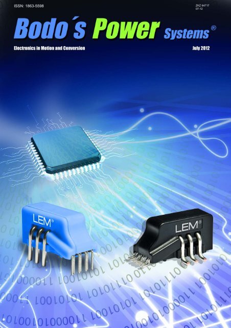
Coverstory<br />
Current Transducers with Advanced ASIC Technology<br />
By Yo Makita, Ph. D, D&E Manager, LEM Japan <strong>and</strong><br />
Stéphane Rollier, Product & MarCom manager,<br />
LEM International SA . . . . . . . . . . . . . . . . . . . . . . . . . . . . . . . 30-33<br />
<strong>Power</strong> Modules<br />
Stacked Substrates for High Voltage Applications<br />
By O. Hohlfeld, R. Bayerer, Th. Hunger, H. Hartung,<br />
Th. Schütze, Inf<strong>in</strong>eon . . . . . . . . . . . . . . . . . . . . . . . . . . . . . . . 34-37<br />
<strong>Power</strong> Modules<br />
Silicon Holds Key to ERP Legislation for Fans <strong>and</strong> Pumps<br />
By Alberto Guerra, International Rectifier . . . . . . . . . . . . . . . . 38-40<br />
Protection<br />
New Symmetric Voltage Suppressor with Peak Pulse <strong>Power</strong> <strong>and</strong><br />
Increased <strong>Power</strong> Capacity<br />
By Alexey Surma, Yury Loktaev, Alex<strong>and</strong>er Stavtsev <strong>and</strong><br />
Anatoly Chernikov, Proton-Electrotex JSC . . . . . . . . . . . . . . . 42-46<br />
Magnetic Components<br />
Higher Performance for Neodymium Magnets<br />
By Takahiro M<strong>in</strong>akuchi, TDK Corporation . . . . . . . . . . . . . . . . 48-51<br />
<strong>Power</strong> Quality<br />
Repetitive Learn<strong>in</strong>g Harmonic Current Control<br />
<strong>in</strong> a Load Emulation System<br />
By Michael Hausmann, Dom<strong>in</strong>ik Dorner, Dr. Norbert Graß<br />
<strong>and</strong> Dr. Bernhard Wagner, Georg Simon Ohm<br />
University of Applied Sciences Nuremberg, Germany . . . . . . 52-55<br />
New Products . . . . . . . . . . . . . . . . . . . . . . . . . . . . . . . . . . . . . 56-64<br />
www.electronicon.com<br />
Scan me for details.<br />
PROBABLY WORLD‘S<br />
MOST COPIED CAPACITOR<br />
(But then: even the closest copy is not the same...)<br />
ELECTRONICON Kondensatoren GmbH · Keplerstrasse 2 · Germany - 07549 Gera<br />
Fon: +49 365 7346 100 · email: sales@electronicon.com · web: www.electronicon.com<br />
www.bodospower.com <strong>July</strong> <strong>2012</strong> Bodo´s <strong>Power</strong> Systems ®<br />
1
2<br />
The Gallery<br />
Bodo´s <strong>Power</strong> Systems ® <strong>July</strong> <strong>2012</strong> www.bodospower.com
F<strong>in</strong>ally! Charge Big Batteries Fast With<br />
4A Chip-Scale Li-Ion Charger ICs<br />
Flexible USB/AC Input from +3.6V to +16V, T<strong>in</strong>y Solution Size, I2C Programmable Parameters <strong>and</strong> Built-In Safety – Ideal for Tablets <strong>and</strong><br />
Smartphones<br />
AC/DC Charger<br />
up to3500mA<br />
4.5V-16V (20V OVP)<br />
VB US D- D+ ID<br />
GND<br />
Features<br />
• +3.6V to +16V Operat<strong>in</strong>g Input (+20V OV Protection)<br />
• Fast-Charg<strong>in</strong>g, Flexible 4A Switch-Mode Architecture<br />
•TurboCharge* current-multiplier cuts charge time by<br />
30%-60%<br />
•TurboCharge+* auto-float voltage control (AFVC) further<br />
reduces charge time by compensat<strong>in</strong>g for <strong>in</strong>ternal battery<br />
impedances<br />
•CurrentPath with dual outputs for system/battery<br />
(SMB349) supports <strong>in</strong>stant-on with dead/miss<strong>in</strong>g battery<br />
•FlexCharge/FlexCharge+* auto power source detection<br />
(APSD/AIVD) per USB2.0/3.0/BC1.2 to detect USB or AC/DC<br />
source +5V to +16V<br />
•OptiCharge* auto <strong>in</strong>put current limit (AICL) detects <strong>and</strong><br />
adapts to source current limit to maximize available power<br />
• I2C Programmable Parameters <strong>and</strong> Functions with NV<br />
Configuration<br />
• SafeCharge safety features support JEITA/IEEE1725<br />
• Battery <strong>and</strong> IC over-voltage/current/temperature<br />
protection<br />
• Trickle charge for deeply-discharged cells<br />
• Safety timers <strong>and</strong> fault monitors/report<strong>in</strong>g<br />
• T<strong>in</strong>y 3.2 x 3.0 CSP <strong>and</strong> 52mm2/1.2mm USB2.0/3.0<br />
500mA/900mA<br />
4.35V-5.5V<br />
z-height solution size<br />
* Patent granted or pend<strong>in</strong>g<br />
USB Input<br />
100/500 /700-3500 mA<br />
USB-OTG/<br />
HDMI/MHL<br />
5.0V @ 900mA<br />
SMB349<br />
H<strong>and</strong>held Device<br />
System Output<br />
up to 4A<br />
"Ideal Diode "<br />
Current<br />
OTG/LBR/HDMI/MHL<br />
~1200 mA<br />
Charg<strong>in</strong>g Current<br />
up to 4A<br />
I2C (optional)<br />
Total Sys. Output<br />
>4A<br />
Applications<br />
• Tablets<br />
• Smartphones<br />
• E-Readers<br />
• UltraBooks<br />
• Battery “JuicePacks”<br />
• Portable Gam<strong>in</strong>g<br />
• Portable Digital Video<br />
Industry’s Highest System<br />
Efficiency<br />
SMB349 SMB359 SMB347 SMB137C SMB346 SMB136C<br />
Input Voltage Range (V)* 4.35 to 16 (20) 4.35 to 16 (20) 4.35 to 6.2 (20) 4.35 to 6.0 (18) 4.35 to 6.2 (20) 4.35 to 6.0 (18)<br />
# of Inputs/Outputs 1/2 1/1 2/2 2/2 2/2 1/2<br />
Maximum Charge Current (mA) 4000 4000 2500 1500 1250 1500<br />
Maximum Input Current (mA) 3500 3500 2500 1500 2500 1500<br />
CurrentPath Control � � � � �<br />
Charge Current Voltage Output � � � �<br />
Low-Battery Recovery Mode � �<br />
Automatic <strong>Power</strong> Source Detection ** rev 1.2 rev 1.2 rev 1.1/1.2 rev 1.2 rev 1.1/1.2 rev 1.2<br />
Package<br />
3.2x3.0 CSP-49<br />
5x5 QFN-40<br />
3.2x3.0 CSP-49<br />
5x5 QFN-40<br />
All chargers have Battery Thermal Protection & JEITA Support, IC Thermal Protection, Auto Input Current Limit, Safety or<br />
Watchdog Timers, Programmable Charg<strong>in</strong>g Parameters, I2C Interface, USB On-The-Go, TurboCharge Mode*<br />
Li- Ion<br />
System<br />
USB<br />
3.0x2.5 CSP-30 3.0x2.5 CSP-30 3.0x2.5 CSP-30 3.0x2.5 CSP-30<br />
Solution Size (mm2) 52 52 32 38 32 35<br />
For more <strong>in</strong>formation see:<br />
www.summitmicro.com/SMB349
VIEWPOINT<br />
A Media<br />
Katzbek 17a<br />
D-24235 Laboe, Germany<br />
Phone: +49 4343 42 17 90<br />
Fax: +49 4343 42 17 89<br />
editor@bodospower.com<br />
www.bodospower.com<br />
Publish<strong>in</strong>g Editor<br />
Bodo Arlt, Dipl.-Ing.<br />
editor@bodospower.com<br />
Creative Direction & Production<br />
Repro Studio Peschke<br />
Repro.Peschke@t-onl<strong>in</strong>e.de<br />
Free Subscription to qualified readers<br />
Bodo´s <strong>Power</strong> Systems<br />
is available for the follow<strong>in</strong>g<br />
subscription charges:<br />
Annual charge (12 issues) is 150 €<br />
world wide<br />
S<strong>in</strong>gle issue is 18 €<br />
subscription@bodospower.com<br />
circulation pr<strong>in</strong>t run<br />
20000<br />
Pr<strong>in</strong>t<strong>in</strong>g by:<br />
Central-Druck Trost GmbH & Co<br />
Heusenstamm, Germany<br />
A Media <strong>and</strong> Bodos <strong>Power</strong> Systems<br />
assume <strong>and</strong> hereby disclaim any<br />
liability to any person for any loss or<br />
damage by errors or omissions <strong>in</strong> the<br />
material conta<strong>in</strong>ed here<strong>in</strong> regardless of<br />
whether such errors result from<br />
negligence accident or any other cause<br />
whatsoever.<br />
Events<br />
SEMICON WEST,<br />
San Francisco CA, <strong>July</strong> 10th -12th<br />
www.semiconwest.org<br />
EPE PEMC,<br />
Novi Sad, Serbia, September 4th-6th<br />
http://epe-pemc<strong>2012</strong>.com/category/news<br />
Battery <strong>Power</strong> <strong>2012</strong>,<br />
Denver Colorado, September 18th -19th<br />
www.batterypoweronl<strong>in</strong>e.com<br />
Thermal Management <strong>2012</strong>,<br />
Denver Colorado,<br />
September 18th -19th<br />
www.thermalnews.com/conferences<br />
LED Professional,<br />
Bregenz Austria,<br />
September 25th -27th<br />
www.led-professional.com/<br />
EU PVSEC,<br />
Frankfurt Germany,<br />
September 24th – 28th<br />
www.photovoltaic-conference.com<br />
Husum W<strong>in</strong>dEnergy,<br />
Husum, Germany, September 18th-22nd<br />
www.husumw<strong>in</strong>denergy.com<br />
Ch<strong>in</strong>a - a Challenge<br />
The Ch<strong>in</strong>ese market challenges all of us <strong>in</strong><br />
the <strong>in</strong>dustry to develop new relationships.<br />
Bodo’s <strong>Power</strong> Ch<strong>in</strong>a has started by cooperat<strong>in</strong>g<br />
with i2i. Serv<strong>in</strong>g such a huge market <strong>in</strong><br />
the local language only makes sense for<br />
reach<strong>in</strong>g out to all eng<strong>in</strong>eers that need upto-date<br />
technical <strong>in</strong>formation. Eng<strong>in</strong>eers,<br />
worldwide, are a rare breed; a po<strong>in</strong>t made by<br />
Alfred Hesener of Fairchild <strong>in</strong> his guest editorial<br />
<strong>in</strong> May. We must do our best to make<br />
technical careers attractive to young people<br />
<strong>and</strong> then provide the support necessary to<br />
have them focus on power electronics.<br />
The <strong>Power</strong>Guru <strong>in</strong>ternet platform will help<br />
students f<strong>in</strong>d articles, products <strong>and</strong> companies<br />
that support their goals for success at<br />
university. Bodo’s <strong>Power</strong> Systems is partner<strong>in</strong>g<br />
with <strong>Power</strong> Guru by provid<strong>in</strong>g the technical<br />
content published <strong>in</strong> our magaz<strong>in</strong>e to the<br />
visitors of their website. Roughly 700 articles<br />
are already available <strong>and</strong> this will cont<strong>in</strong>ue<br />
for future issues.<br />
I’d like to welcome Marisa Robles Consée<br />
who will, <strong>in</strong> the future, support us as a freelance<br />
journalist with a focus on press events<br />
<strong>in</strong> Bavaria. I am very happy to have such an<br />
experienced editor on my team. The magaz<strong>in</strong>e<br />
has progressed, along with the <strong>in</strong>dustry,<br />
<strong>and</strong> we must provide effective support for<br />
media service needs. Intersolar <strong>in</strong> Munich<br />
was the first event that Marisa covered for<br />
us.<br />
Be<strong>in</strong>g <strong>in</strong> Shanghai for the PCIM Conference<br />
<strong>and</strong> Show has opened up my view of Ch<strong>in</strong>a.<br />
This strong <strong>and</strong> grow<strong>in</strong>g nation left a last<strong>in</strong>g<br />
impression of Asia as a region that moves<br />
very fast!<br />
Communication is the only way to progress.<br />
We delivered twelve issues last year <strong>and</strong> will<br />
cont<strong>in</strong>ue each month, on time, every time.<br />
So far this year we have published 508<br />
pages <strong>and</strong> 84 technical articles. As a media<br />
partner, Bodo’s <strong>Power</strong> Systems is <strong>in</strong>ternationally<br />
positioned. Don’t miss our Ch<strong>in</strong>ese<br />
version: www.bodospowerch<strong>in</strong>a.com.<br />
My Green <strong>Power</strong> Tip for <strong>July</strong>:<br />
Whenever possible, use the <strong>in</strong>ternet <strong>and</strong><br />
phone calls <strong>in</strong>stead of travell<strong>in</strong>g. This will<br />
save some of the world’s energy resources.<br />
Plan ahead <strong>and</strong> bundle your travel activity to<br />
maximize effectiveness <strong>and</strong> m<strong>in</strong>imize energy<br />
consumption.<br />
Best<br />
regards<br />
4 Bodo´s <strong>Power</strong> Systems ® <strong>July</strong> <strong>2012</strong> www.bodospower.com
Dawn of a new <strong>in</strong>telligence<br />
for current measurement<br />
��<br />
������������� �������� ������������ ���� ������ ���� ���� ��� ������������� �����������<br />
����������� ������� ����� ���� ����� ��� ���� ������������� ���� ���� ���� �����������<br />
��������������� ����� � ������ ��������������� ��������� �� ���� ���� �������������<br />
���������������������������������������������������������������� ��������� ���<br />
���������������������������������������������������������������������������������<br />
����������������������<br />
� ���������������������������<br />
������������ ��������� ���<br />
� ��������������������������������<br />
� �����������������������������<br />
� ����������������������������������<br />
����������������������������������������<br />
� �����������������������������������<br />
�������� ����������<br />
� ���������������������������<br />
������������ ����������<br />
� ���������������������������������<br />
�������������<br />
� ������������������������������<br />
�������������������<br />
� ����������������������������<br />
� �����������������������<br />
www.lem.com At the heart of power electronics.
NEWS<br />
HUSUM is the Natural Home of W<strong>in</strong>d<br />
From 18 - 22 September, the global w<strong>in</strong>d <strong>in</strong>dustry will once aga<strong>in</strong> be<br />
centred on HUSUM, the natural home of w<strong>in</strong>d. This small town on the<br />
North Sea coast of Germany has been the shop w<strong>in</strong>dow of the w<strong>in</strong>d<br />
world s<strong>in</strong>ce 1989, show<strong>in</strong>g the latest w<strong>in</strong>d technology, associated<br />
products <strong>and</strong> services from all over the world.<br />
As the <strong>in</strong>dustry has developed over the last two decades, HUSUM<br />
W<strong>in</strong>dEnergy has been the natural magnet for all those want<strong>in</strong>g to see<br />
the latest products the <strong>in</strong>dustry has to offer. Whether these are<br />
improvements <strong>in</strong> onshore technology aimed at improv<strong>in</strong>g perform-<br />
SemiSouth Garners 30 th US Patent<br />
SemiSouth Laboratories, Inc. is pleased to<br />
announce its 30th US patent granted by the<br />
US Patent <strong>and</strong> Trademark Office. Semi-<br />
South is an <strong>in</strong>dustry leader <strong>in</strong> design<strong>in</strong>g <strong>and</strong><br />
manufactur<strong>in</strong>g silicon-carbide (SiC) power<br />
semiconductor transistors <strong>and</strong> diodes, which<br />
are rapidly ga<strong>in</strong><strong>in</strong>g market share <strong>in</strong> the solar,<br />
UPS, traction, w<strong>in</strong>d, automotive, <strong>and</strong> aerospace<br />
<strong>in</strong>dustries for their superior performance<br />
<strong>in</strong> high-efficiency, harsh-environment<br />
power applications.<br />
US Patent 8,169,022 was issued on May 1,<br />
<strong>2012</strong>, <strong>and</strong> is entitled “Vertical Junction Field<br />
CUI Launched New Website<br />
CUI Inc announced the launch of its new<br />
website, www.cui.com. A ma<strong>in</strong> feature of the<br />
new site is a significantly advanced parametric<br />
search capability for the company’s<br />
<strong>Power</strong>, <strong>Motion</strong> Control, <strong>and</strong> Components<br />
product l<strong>in</strong>es. Visitors to the new site are<br />
now able to dynamically filter, sort, <strong>and</strong> send<br />
searches based on a range of critical specifications.<br />
Access to technical resources has<br />
been greatly improved <strong>and</strong> now <strong>in</strong>cludes<br />
downloadable 3D models, videos, <strong>and</strong> application<br />
notes, with no registration required.<br />
The new site also highlights the latest news<br />
Effect Transistors <strong>and</strong> Diodes Hav<strong>in</strong>g Graded<br />
Doped Regions <strong>and</strong> Methods of Mak<strong>in</strong>g.”<br />
It was co-<strong>in</strong>vented by Dr. Michael Mazzola, a<br />
co-founder of SemiSouth <strong>in</strong> 2000 when the<br />
company spun off of Mississippi State University.<br />
“The underly<strong>in</strong>g technology <strong>in</strong> this patent<br />
allows SemiSouth to f<strong>in</strong>e tune their already<br />
performance-lead<strong>in</strong>g vertical channel junction<br />
field effect transistors <strong>and</strong> diodes to get<br />
ever closer to the unipolar theoretical limit.<br />
Customers can expect even better value<br />
from the products based on this patent,” said<br />
ance <strong>and</strong> efficiency, new developments to ensure the stability of offshore<br />
turb<strong>in</strong>e foundations, or flexible grid solutions, HUSUM rema<strong>in</strong>s<br />
the most important source of <strong>in</strong>formation for players at all levels.<br />
Now head<strong>in</strong>g towards its quarter century, HUSUM W<strong>in</strong>dEnergy<br />
boasts 1,200 exhibitors from over 30 nations, <strong>and</strong> more than 36,000<br />
visitors from over 90 countries.<br />
When the first Husum W<strong>in</strong>d Days were held back <strong>in</strong> 1989, the pioneer<br />
turb<strong>in</strong>e builders were not taken seriously by ma<strong>in</strong>stream energy<br />
providers, <strong>and</strong> the number of politicians who were able to grasp what<br />
was go<strong>in</strong>g on could be counted on one h<strong>and</strong>, HUSUM showed the<br />
way ahead. And today, with a resurgence of the (onshore) w<strong>in</strong>d<br />
power objectors <strong>in</strong> many countries, HUSUM is where the doubters<br />
can separate fact from fiction <strong>and</strong> then make qualified decisions<br />
about their energy future.<br />
The HUSUM W<strong>in</strong>dEnergy Congress is an established forum for present<strong>in</strong>g<br />
new technology <strong>and</strong> discuss<strong>in</strong>g the new challenges fac<strong>in</strong>g<br />
the <strong>in</strong>dustry. With fears of economic meltdown <strong>in</strong> the Eurozone, <strong>and</strong><br />
the cont<strong>in</strong>ued impact of the global bank<strong>in</strong>g crisis, it has never been<br />
more important for all w<strong>in</strong>d <strong>in</strong>dustry actors to come together to help<br />
shape the future. The congress covers onshore <strong>and</strong> offshore developments,<br />
present <strong>and</strong> future challenges fac<strong>in</strong>g the <strong>in</strong>dustry, advice<br />
about fund<strong>in</strong>g communal <strong>and</strong> large-scale <strong>in</strong>dustrial projects, new<br />
developments <strong>in</strong> the fields of lubrication <strong>and</strong> weather prediction, <strong>and</strong><br />
company <strong>in</strong>novations from well-established enterprises <strong>and</strong> young<br />
trailblazers.<br />
www.husumw<strong>in</strong>denergy.com<br />
Mazzola. “We are excited to receive our<br />
30th US patent,” said Dr. Jeffrey B. Casady,<br />
SemiSouth President & CTO <strong>and</strong> company<br />
co-founder. “Our technology is state-of-theart<br />
<strong>in</strong> terms of performance per unit area.<br />
SemiSouth products deliver advanced, efficient,<br />
cost-effective power solutions that others<br />
cannot.” In addition to 30 US patents,<br />
SemiSouth possesses 24 patents <strong>in</strong>ternationally<br />
<strong>and</strong> has 204 applications pend<strong>in</strong>g<br />
worldwide.<br />
www.semisouth.com<br />
<strong>and</strong> social media feeds from CUI.<br />
“We developed the new cui.com with the<br />
goal of mak<strong>in</strong>g our product l<strong>in</strong>es easy to<br />
navigate <strong>and</strong> our content simple to access<br />
for the eng<strong>in</strong>eer<strong>in</strong>g community.<br />
We believe visitors will f<strong>in</strong>d our new site<br />
greatly improved while still ma<strong>in</strong>ta<strong>in</strong><strong>in</strong>g some<br />
of the exist<strong>in</strong>g functionality that made our<br />
previous site successful,” stated CUI’s VP<br />
Market<strong>in</strong>g, Jeff Schnabel.<br />
www.cui.com<br />
6 Bodo´s <strong>Power</strong> Systems ® Bodo´s <strong>Power</strong> Systems <strong>July</strong> <strong>2012</strong> www.bodospower.com<br />
® <strong>July</strong> <strong>2012</strong> www.bodospower.com
Does your digital power-supply design controller require<br />
high performance flexible on-chip peripherals?...<br />
Control complex Digital <strong>Power</strong> applications <strong>and</strong> save power<br />
Microchip’s new dsPIC33F ‘GS’ Series DSCs provide on-chip peripherals<br />
<strong>in</strong>clud<strong>in</strong>g high-speed Pulse-Width-Modulators (PWMs), ADCs <strong>and</strong><br />
analogue comparators, specifically designed for high performance, digital<br />
power supplies.<br />
The powerful dsPIC33F ‘GS’ series is specifically aimed at power control<br />
applications <strong>and</strong> can be configured for a variety of topologies, giv<strong>in</strong>g powersupply<br />
designers the complete freedom to optimise for specific product<br />
applications. Multiple <strong>in</strong>dependent power control channels enable an<br />
unprecedented number of completely <strong>in</strong>dependent digital control loops.<br />
The dsPIC33F ‘GS’ series offers the optimal digital power solution supported by<br />
royalty free reference designs <strong>and</strong> advanced power design tools.<br />
Typical applications for the new ‘GS’ series DSC <strong>in</strong>clude: Light<strong>in</strong>g (HID, LED ,<br />
fluorescent), un<strong>in</strong>terruptable power supplies, <strong>in</strong>telligent battery chargers,<br />
AC-DC <strong>and</strong> DC-DC power converters, solar <strong>and</strong> pure s<strong>in</strong>e-wave <strong>in</strong>verters,<br />
<strong>in</strong>duction cook<strong>in</strong>g, <strong>and</strong> power factor correction.<br />
� Digital control loops with up to 18 high-speed, 1 ns resolution PWMs<br />
� Up to 24 channels 10-bit on-chip ADCs<br />
� 2 to 4 Million Samples Per Second (MSPS) ADC for low latency <strong>and</strong><br />
high-resolution control<br />
� P<strong>in</strong> range: 18 to 64<br />
� Up to 64KB Flash memory<br />
GET STARTED IN<br />
3 EASY STEPS:<br />
1. Purchase a ‘GS’ Series<br />
Plug-In Module<br />
2. Download Digital <strong>Power</strong><br />
Reference Design<br />
3. Order samples <strong>and</strong> start<br />
design<strong>in</strong>g!<br />
www.microchip.com/power<br />
For more <strong>in</strong>formation, go to: www.microchip.com/power<br />
The Microchip name <strong>and</strong> logo are registered trademarks of Microchip Technology Incorporated <strong>in</strong> the USA <strong>and</strong> other countries. All other trademarks are the property of their respective owners.<br />
© <strong>2012</strong> Microchip Technology Inc. All rights reserved. ME1035-Eng06.12<br />
dsPIC33F ‘GS’ Series Plug-In Module<br />
(MA330024)
NEWS<br />
High-Efficiency Bifacial Silicon Solar Cells<br />
bSolar announced the availability of its highpower,<br />
high-efficiency, bifacial, photovoltaic<br />
(PV), crystall<strong>in</strong>e silicon solar cells. Bifacial<br />
cells utilize the cells' rear side to collect<br />
reflected <strong>and</strong> diffused sunlight to generate<br />
additional electricity. bSolar cells are produced<br />
us<strong>in</strong>g p-type wafers, st<strong>and</strong>ard equipment<br />
<strong>and</strong> production processes, giv<strong>in</strong>g them<br />
a mass market appeal.<br />
The new cells provide 10-30% higher energy<br />
(KWH) per KWp <strong>in</strong>stalled <strong>in</strong> st<strong>and</strong>ard applications<br />
<strong>and</strong> up to 50% <strong>in</strong> vertical <strong>in</strong>stallations,<br />
result<strong>in</strong>g <strong>in</strong> an equivalent cell efficiency<br />
of 21%-24% <strong>in</strong> st<strong>and</strong>ard applications <strong>and</strong><br />
a total module power of 280-325 Watts for<br />
60 cell modules. This unprecedented efficiency<br />
<strong>and</strong> power are amongst the <strong>in</strong>dustry<br />
highest for mono crystall<strong>in</strong>e silicon cells.<br />
Applications for the new cells <strong>in</strong>clude flat<br />
rooftops <strong>and</strong> ground <strong>in</strong>stallations, as well as<br />
unique solutions for special BIPV applications<br />
such as solar sound barriers, car ports,<br />
facades <strong>and</strong> green houses.<br />
The bifacial cells are produced <strong>in</strong> bSolar’s<br />
New Manufactur<strong>in</strong>g Facility <strong>in</strong> Rome, NY<br />
Indium Corporation has acquired a new<br />
manufactur<strong>in</strong>g facility, located at 5836 Success<br />
Drive, Rome, NY, USA. The plant is<br />
currently be<strong>in</strong>g outfitted to exp<strong>and</strong> production<br />
capacities of Indium Corporation’s range<br />
of compounds, <strong>in</strong>clud<strong>in</strong>g <strong>in</strong>dium-, gallium-,<br />
germanium-, <strong>and</strong> t<strong>in</strong>-based materials.<br />
The company’s expansion addresses its<br />
grow<strong>in</strong>g global success with supply<strong>in</strong>g materials<br />
to <strong>in</strong>dustries such as solar photovoltaic,<br />
flat panel display, semiconductor, optical<br />
fiber, LED, <strong>and</strong> others.<br />
Indium Corporation is <strong>in</strong>stall<strong>in</strong>g state-of-theart<br />
manufactur<strong>in</strong>g equipment, processes,<br />
<strong>and</strong> analytical capabilities to address the<br />
world’s dem<strong>and</strong> for high-performance materials.<br />
The enhanced capabilities will enable<br />
Indium Corporation to convert a wider range<br />
of feed materials <strong>in</strong>to high-purity compounds<br />
<strong>and</strong> provide recycl<strong>in</strong>g of customers’ reclaim<br />
streams.<br />
Accord<strong>in</strong>g to Claire Mikolajczak, Indium Corporation’s<br />
Director of Metals <strong>and</strong> Compounds,<br />
“This major expansion enables us to simultaneously<br />
enhance our process efficiencies,<br />
product quality, <strong>and</strong> product range. We will<br />
soon be able to deliver a very large share of<br />
the world’s dem<strong>and</strong> for high quality compounds.”<br />
<strong>in</strong>dustrial production l<strong>in</strong>e <strong>in</strong> Heilbronn, Germany<br />
<strong>and</strong> have been recently <strong>in</strong>corporated<br />
<strong>in</strong>to bifacial modules by numerous producers<br />
worldwide. The current production capacity<br />
of bSolar is 30 MWp/year <strong>and</strong> the company<br />
is plann<strong>in</strong>g to rapidly exp<strong>and</strong> production to<br />
meet customer dem<strong>and</strong>.<br />
"We are excited to <strong>in</strong>troduce our disruptive<br />
bifacial cells, which will significantly improve<br />
the f<strong>in</strong>ancial returns of solar projects.", commented<br />
Yossi Kofman, bSolar’s CEO. "We<br />
are currently work<strong>in</strong>g with our commercial<br />
partners <strong>and</strong> customers to br<strong>in</strong>g cutt<strong>in</strong>g-edge<br />
bifacial panels to the market."<br />
www.b-solar.com<br />
Greg Evans, Indium Corporation President,<br />
added,<br />
“We have committed to our markets that we<br />
will raise the bar with regard to capacity,<br />
quality, <strong>and</strong> service. Our new facility<br />
addresses each of these issues <strong>and</strong> even<br />
allows us to partner with new customers on<br />
their challeng<strong>in</strong>g future requirements. We<br />
look forward to these new opportunities.”<br />
The new plant is sized to accommodate<br />
future expansion of upstream <strong>and</strong> downstream<br />
processes to improve its costs <strong>and</strong><br />
performance.<br />
www.<strong>in</strong>dium.com<br />
25 Years of Success<br />
Syfer Technology are celebrat<strong>in</strong>g 25 years of successful electronic<br />
component development at their Norwich headquarters <strong>and</strong> are set to<br />
cont<strong>in</strong>ue their <strong>in</strong>novation serv<strong>in</strong>g new markets.<br />
Syfer Technology, which employs 240 people, is Europe’s lead<strong>in</strong>g<br />
manufacturer of ceramic multilayer capacitors, which are widely used<br />
<strong>in</strong> telecommunications, automotive manufacture <strong>and</strong> other <strong>in</strong>dustrial<br />
applications.<br />
Over the last 25 years Syfer have shown their skill <strong>and</strong> flexibility <strong>in</strong><br />
be<strong>in</strong>g able to adapt their operations to meet new trends <strong>and</strong> emerg<strong>in</strong>g<br />
markets.<br />
“We have successfully identified new customers <strong>in</strong> different areas like<br />
medical <strong>in</strong>strumentation, military applications, the aerospace <strong>in</strong>dustry<br />
<strong>and</strong> space exploration,” says Howard Ingleson, Syfer Technology’s<br />
Manag<strong>in</strong>g Director.<br />
“Many of the products that are made with our electronics components<br />
are used <strong>in</strong> safety-critical environments, <strong>and</strong> so precision <strong>and</strong> quality<br />
are paramount,” he says.<br />
The company has pioneered several cutt<strong>in</strong>g-edge production techniques<br />
<strong>and</strong> component designs to meet global market requirements. www.syfer.com<br />
8 Bodo´s <strong>Power</strong> Systems ® Bodo´s <strong>Power</strong> Systems June <strong>2012</strong> www.bodospower.com<br />
® <strong>July</strong> <strong>2012</strong> www.bodospower.com
Extension of the HelioProtection ® Program Offer<strong>in</strong>g<br />
Mersen has identified specific needs for universal<br />
<strong>and</strong> high-quality monitor<strong>in</strong>g systems.<br />
These needs are related to PV <strong>in</strong>stallations<br />
<strong>in</strong> <strong>in</strong>dustrial <strong>and</strong> commercial fields <strong>and</strong> large<br />
solar farms as well. For such <strong>in</strong>stallation the<br />
<strong>in</strong>vestor is wait<strong>in</strong>g quick <strong>and</strong> good return on<br />
<strong>in</strong>vestment. Mersen has designed a set of<br />
electronic cards for monitor<strong>in</strong>g. At the core is<br />
the ma<strong>in</strong> electronic card capable of monitor<strong>in</strong>g<br />
six str<strong>in</strong>gs mak<strong>in</strong>g it possible to detect<br />
problems as they occur by spott<strong>in</strong>g their precise<br />
location <strong>in</strong> the str<strong>in</strong>g. Auxiliary cards can<br />
be added <strong>in</strong> order to monitor up to 30 str<strong>in</strong>gs<br />
<strong>in</strong> total.<br />
Edouard Guillaume, Product Manager<br />
states: “The ma<strong>in</strong> card <strong>and</strong> four additional<br />
auxiliary cards can be <strong>in</strong>stalled <strong>in</strong> Mersen's<br />
HelioProtection? junction boxes to monitor<br />
solar panel str<strong>in</strong>gs.The benefits <strong>in</strong>clude<br />
proactive ma<strong>in</strong>tenance, an <strong>in</strong>crease <strong>in</strong> the<br />
power performance of the system (an<br />
improved rate of energy actually produced<br />
compared with theoretical energy production)<br />
<strong>and</strong> more secure return on <strong>in</strong>vestment,<br />
with greater profits <strong>and</strong> operational costs<br />
under control.”<br />
Mersen's HelioProtection? junction boxes<br />
<strong>in</strong>corporat<strong>in</strong>g self-powered monitor<strong>in</strong>g electronic<br />
cards enable various monitor<strong>in</strong>g <strong>and</strong><br />
diagnostic functions to be embedded <strong>in</strong><br />
order to manage energy generation <strong>and</strong><br />
equipment ma<strong>in</strong>tenance.<br />
PV Fire Shunt jo<strong>in</strong>s HelioProtection ® Program<br />
Different national guidel<strong>in</strong>es recommend that<br />
<strong>in</strong> solar PV <strong>in</strong>stallations the DC circuit be<br />
switched off the closest to PV modules so as<br />
to secure the <strong>in</strong>tervention of emergency<br />
responders.<br />
Mersen has designed an <strong>in</strong>novative solution<br />
to meet this requirement for safety. The PV<br />
Fire Shunt device designed by Mersen is<br />
based on a shunt technology <strong>in</strong> order to<br />
lower the voltage to almost 0V. This is<br />
achieved by pull<strong>in</strong>g straight down one h<strong>and</strong>le<br />
with a pike pole. This technology plus the<br />
product’s mechanical characteristics, thanks<br />
to materials guarantee<strong>in</strong>g good resistance to<br />
fire <strong>and</strong> flames, secure the area for emergency<br />
responders <strong>and</strong> fire fighters. One PV<br />
Fire Shunt secures 3 PV str<strong>in</strong>gs which is the<br />
case <strong>in</strong> residential PV <strong>in</strong>stallations.<br />
LED Component Bus<strong>in</strong>ess Keeps Grow<strong>in</strong>g<br />
Luger Research, the organizers of the LpS LED professional Symposium<br />
+Expo <strong>2012</strong> announced that the exhibition that runs parallel to<br />
the symposium has already sold 2/3 of its exhibitor spaces with still<br />
4 months left until the start of the symposium.<br />
The exhibitor list is very impressive with many major players <strong>and</strong><br />
specialist companies from the LED <strong>in</strong>dustry exhibit<strong>in</strong>g <strong>in</strong> Bregenz for<br />
the second time runn<strong>in</strong>g or participat<strong>in</strong>g for the first time this year.<br />
Among them are companies like e:lumix, Osram, Tridonic, Alanod,<br />
AT&S, Bergquist, Cree, Everlight <strong>and</strong> Zenaro, to name just a few.<br />
A complete exhibitor list is available at: http://www.led-professionalsymposium.com/exhibition/lps-<strong>2012</strong>-exhibitor-list<br />
Visitors travel from around the world to meet <strong>in</strong> September at the<br />
famous Festspielhaus <strong>in</strong> Bregenz, Austria for this event. They come<br />
from a wide range of lum<strong>in</strong>ary <strong>and</strong> light<strong>in</strong>g <strong>in</strong>dustries. In 2011 20% of<br />
the visitors were <strong>in</strong>volved <strong>in</strong> lum<strong>in</strong>ary & light<strong>in</strong>g system manufactur<strong>in</strong>g,<br />
12% came from research & education, 9% from distribution, 7%<br />
from LED manufactur<strong>in</strong>g, 6% were <strong>in</strong>volved <strong>in</strong> eng<strong>in</strong>eer<strong>in</strong>g & design<br />
services, 5% were driver & supply manufacturers, 4% each were<br />
electronic component manufacturers, lamp manufacturers <strong>and</strong> consultants.<br />
The LED professional Symposium & Exhibition targets <strong>in</strong>terest<br />
groups that are look<strong>in</strong>g for <strong>in</strong>formation about LED light<strong>in</strong>g technolo-<br />
www.bodospower.com <strong>July</strong> <strong>2012</strong> Bodo´s <strong>Power</strong> Systems ®<br />
NEWS<br />
Extension of HelioProtection ® gPV fuse<br />
l<strong>in</strong>ks mapp<strong>in</strong>g<br />
Mersen pursues the development of its<br />
HelioProtection? gPV fuse l<strong>in</strong>ks offer<strong>in</strong>g.<br />
Besides the gPV str<strong>in</strong>g fuse l<strong>in</strong>ks: HP6M<br />
(10x38mm), HP10M (10x38mm), DC10<br />
(10x85mm) Mersen launches new gPV ma<strong>in</strong><br />
fuse l<strong>in</strong>ks comply<strong>in</strong>g with the well renowned<br />
NH st<strong>and</strong>ard (square-bodied fuse l<strong>in</strong>ks with<br />
blade-type connections).<br />
Emmanuelle Delcambre, Product Manager<br />
states: “For 1000VDC we offer now a ‘short’<br />
NH size 1 with rat<strong>in</strong>gs from 50A to 160A <strong>and</strong><br />
a ‘long’ NH size 3 with rat<strong>in</strong>gs from 250A to<br />
400A.”<br />
The completion of the mapp<strong>in</strong>g will be<br />
achieved with the launch of the 1500VDC<br />
NH model at end <strong>2012</strong>.<br />
Innovative fuseholder with screwless,<br />
spr<strong>in</strong>g pressure, wire term<strong>in</strong>ation technology<br />
Mersen launches a new UltraSafe fuse<br />
holder for 10x38 sized fuse l<strong>in</strong>ks.<br />
USGM1HEL fuse holder is easy to use <strong>and</strong><br />
save time for <strong>in</strong>stallers. It’s a safe <strong>and</strong> reliable<br />
solution for PV <strong>in</strong>stallations market.<br />
“Easy wir<strong>in</strong>g is of course the key feature of<br />
this new product. Another key feature is the<br />
limitation of DC effects on the wir<strong>in</strong>g provided<br />
by the Wago Cage Clamp® technology.”,<br />
states Franck Ageron, Product Manager.<br />
www.mersen.com<br />
gies <strong>and</strong> its applications <strong>in</strong> light modules <strong>and</strong> light<strong>in</strong>g elements. The<br />
symposium is technology oriented <strong>and</strong> therefore ideal for specialists<br />
from the research <strong>and</strong> <strong>in</strong>dustry. In 8 sessions 26 speakers cover a<br />
multitude of LED topics that attract an expert audience, br<strong>in</strong>g<strong>in</strong>g high<br />
quality leads to the exhibition. The exhibition is a perfect platform to<br />
present technologies <strong>and</strong> implementation solutions <strong>and</strong> to demonstrate<br />
products <strong>and</strong> services to global decision makers <strong>and</strong> to an<br />
extended circle of delegates from major <strong>in</strong>dustry players.<br />
The Symposium <strong>and</strong> Expo will be held aga<strong>in</strong> at the Festspielhaus <strong>in</strong><br />
Bregenz. For this year the exhibition area has been exp<strong>and</strong>ed to<br />
accommodate the <strong>in</strong>creas<strong>in</strong>g number of exhibitors. The presentations<br />
will be held <strong>in</strong> the “Grosser Saal” which is equipped with the latest<br />
presentation technology ensur<strong>in</strong>g a high quality experience.<br />
Besides host<strong>in</strong>g the world renowned annual Bregenz Festival,<br />
scenes from the James Bond film, Quantum of Solace, were filmed<br />
here.<br />
www.lps<strong>2012</strong>.com<br />
9
NEWS<br />
Peter Schiefer Appo<strong>in</strong>ted Head of Operations<br />
Inf<strong>in</strong>eon Technologies announced that<br />
Peter Schiefer (46) will assume leadership<br />
of Operations at Inf<strong>in</strong>eon Technologies<br />
AG as of September 1, <strong>2012</strong>. He<br />
will report to Dr. Re<strong>in</strong>hard Ploss, member<br />
of the Management Board, <strong>and</strong> be<br />
responsible for the company’s Manufactur<strong>in</strong>g,<br />
Supply Cha<strong>in</strong> <strong>and</strong> Purchas<strong>in</strong>g<br />
activities. Peter Schiefer will simultaneously<br />
give up his position as Head of the<br />
<strong>Power</strong> Management & Multimarket<br />
(PMM) Division, which he has led s<strong>in</strong>ce<br />
January 1, <strong>2012</strong>.<br />
As of September 1, <strong>2012</strong>, the new Head of the <strong>Power</strong> Management<br />
& Multimarket (PMM) Division will be Andreas Urschitz (40). As a<br />
Photo Voltaic Meets Manufactur<strong>in</strong>g<br />
Where do PV manufacturers go to meet<br />
up with equipment <strong>and</strong> materials suppliers<br />
to identify critical manufactur<strong>in</strong>g<br />
needs? How do they determ<strong>in</strong>e mean<strong>in</strong>gful<br />
action items to accelerate <strong>in</strong>dustry<br />
growth?<br />
SEMI has created the best possible<br />
place to meet PV equipment <strong>and</strong> materials<br />
companies <strong>in</strong> one venue <strong>and</strong> network<br />
<strong>and</strong> collaborate on major issues<br />
fac<strong>in</strong>g the <strong>in</strong>dustry. At the Intersolar<br />
Europe, SEMI PV Group has organized<br />
a wide variety of special events, meet<strong>in</strong>gs, <strong>and</strong> exhibits geared for<br />
solar energy professionals <strong>in</strong>volved <strong>in</strong> the manufactur<strong>in</strong>g supply<br />
James Doyle Appo<strong>in</strong>ted President <strong>and</strong> CEO<br />
The Owners <strong>and</strong> Board of Directors of<br />
RF <strong>and</strong> microwave components manufacturer,<br />
XMA Corporation, announced<br />
today that they have appo<strong>in</strong>ted James<br />
Doyle as the company’s new President<br />
<strong>and</strong> CEO.<br />
“Our leadership committee considered<br />
many extraord<strong>in</strong>ary c<strong>and</strong>idates for this<br />
position dur<strong>in</strong>g a nationwide search, but<br />
it became very clear to all that James<br />
Doyle was the right choice to lead the<br />
organization <strong>and</strong> create a new vision for<br />
the future,” said Fred Goodrich, XMA’s Board Chairman. “James is a<br />
leader, with <strong>in</strong>-depth knowledge <strong>and</strong> experience, <strong>and</strong> is highly results<br />
driven. He has an authentic passion for our mission to make XMA<br />
the premier supplier for highly complex RF term<strong>in</strong>ation <strong>and</strong><br />
microwave <strong>in</strong>terconnect systems. XMA Corporation is now poised for<br />
tremendous growth, <strong>and</strong> we are eager to welcome James to lead the<br />
organization <strong>in</strong> the next steps of our evolution.”<br />
member of the PMM management he is currently responsible for<br />
worldwide Sales, Market<strong>in</strong>g <strong>and</strong> Distribution of the division. He will<br />
cont<strong>in</strong>ue these activities.<br />
After study<strong>in</strong>g bus<strong>in</strong>ess at the Vienna University of Economics <strong>and</strong><br />
Bus<strong>in</strong>ess Adm<strong>in</strong>istration <strong>and</strong> his teach<strong>in</strong>g activities there, Andreas<br />
Urschitz began work<strong>in</strong>g <strong>in</strong> the semiconductor <strong>in</strong>dustry at Siemens<br />
<strong>and</strong> later Inf<strong>in</strong>eon <strong>in</strong> 1994. After hold<strong>in</strong>g senior management positions<br />
<strong>in</strong> production plann<strong>in</strong>g, market<strong>in</strong>g <strong>and</strong> strategy, he took over as Head<br />
of Market<strong>in</strong>g for power semiconductors. In 2005, he assumed worldwide<br />
responsibility for <strong>Power</strong> Management & Supply Discretes. S<strong>in</strong>ce<br />
January 1, <strong>2012</strong>, he has been a member of the management of the<br />
<strong>Power</strong> Management & Multimarket (PMM) Division, where he is<br />
responsible for global Sales, Market<strong>in</strong>g <strong>and</strong> Distribution.<br />
www.<strong>in</strong>f<strong>in</strong>eon.com<br />
cha<strong>in</strong>. From the 8th Advanced PV Manufactur<strong>in</strong>g Forum to the PV<br />
Production <strong>and</strong> Technology Hall A5 & A6 to the PV St<strong>and</strong>ards development<br />
meet<strong>in</strong>gs, it's the place to learn how to ga<strong>in</strong> traction <strong>in</strong> the<br />
PV manufactur<strong>in</strong>g.<br />
The 8th Advanced PV Manufactur<strong>in</strong>g Forum had been an excellent<br />
opportunity for PV technology leaders, managers, eng<strong>in</strong>eers <strong>and</strong> professionals<br />
from the manufactur<strong>in</strong>g, supplier <strong>and</strong> R&D communities to<br />
share their most recent developments <strong>in</strong> the collective drive towards<br />
quality <strong>and</strong> excellence <strong>in</strong> PV manufactur<strong>in</strong>g.<br />
www.semi.org/europe<br />
www.pvgroup.org<br />
Doyle is an accomplished leader with a proven track record of creat<strong>in</strong>g<br />
well-targeted strategies that achieve bus<strong>in</strong>ess objectives. Most<br />
recently he worked as the Congressional Affairs Liaison for Emerson<br />
Embedded Comput<strong>in</strong>g <strong>in</strong> Wash<strong>in</strong>gton DC, a “Fortune 100” company.<br />
He is highly regarded <strong>in</strong> the technology <strong>in</strong>dustry <strong>and</strong> considered one<br />
of the lead<strong>in</strong>g authorities on the chang<strong>in</strong>g face of Wash<strong>in</strong>gton, D.C.<br />
Previous to his appo<strong>in</strong>tment with Emerson he was the Vice President<br />
of Bus<strong>in</strong>ess Development <strong>and</strong> Strategy for Hybricon Corporation. He<br />
holds degrees from the University of Massachusetts <strong>and</strong> an MBA<br />
from Boston University.<br />
“I am excited to have the opportunity to lead this world-class organization,”<br />
said Doyle. “XMA has a tremendous reputation <strong>and</strong> a strong<br />
history thanks to the passion <strong>and</strong> expertise of past <strong>and</strong> present leadership.<br />
I am confident that we can create even greater value to our<br />
customers <strong>and</strong> stakeholders go<strong>in</strong>g forward.”<br />
www.xmacorp.com<br />
10 Bodo´s <strong>Power</strong> Systems ® <strong>July</strong> <strong>2012</strong> www.bodospower.com
Ploessl Named Compounds<br />
Product Manager<br />
Indium Corporation announces that<br />
Robert Ploessl, PhD, has been named<br />
Product Manager for <strong>in</strong>dium, gallium,<br />
germanium <strong>and</strong> t<strong>in</strong> compounds.<br />
Dr. Ploessl will work with Indium’s global<br />
team of eng<strong>in</strong>eer<strong>in</strong>g, sales, operations,<br />
<strong>and</strong> research <strong>and</strong> development professionals<br />
to capitalize on the growth of<br />
LEDs, metal organic precursors, power<br />
storage systems, fiber optics, <strong>and</strong> the<br />
next generation OLED displays. He will<br />
develop Indium Corporation’s market<strong>in</strong>g<br />
strategies, while br<strong>in</strong>g<strong>in</strong>g <strong>in</strong>sights<br />
learned from their technical team to further product development<br />
efforts. Indium Corporation’s compounds bus<strong>in</strong>ess <strong>in</strong>cludes <strong>in</strong>dium<br />
trichloride (InCl3), gallium trichloride (GaCl3), germanium tetrachloride<br />
(GeCl4), as well as a full range of oxides.<br />
Dr. Ploessl jo<strong>in</strong>ed Indium Corporation <strong>in</strong> 2010. He holds a doctorate<br />
<strong>in</strong> physics from the University of Regensburg <strong>in</strong> Germany <strong>and</strong> an<br />
MBA from the S.C. Johnson Graduate School of Management at Cornell<br />
University.<br />
Dr. Ploessl is based at Indium Corporation’s Global Headquarters <strong>in</strong><br />
Cl<strong>in</strong>ton, NY, <strong>and</strong> resides <strong>in</strong> New Hartford.<br />
www.bodospower.com<br />
www.<strong>in</strong>dium.com<br />
Dr. David Reusch Jo<strong>in</strong>s<br />
Efficient <strong>Power</strong> <strong>Conversion</strong><br />
Efficient <strong>Power</strong> <strong>Conversion</strong> Corporation (EPC) is proud to announce<br />
that Dr. David Reusch has jo<strong>in</strong>ed the EPC eng<strong>in</strong>eer<strong>in</strong>g team as<br />
Director, Applications Eng<strong>in</strong>eer<strong>in</strong>g.<br />
As a member of the EPC applications team, Dr. Reusch’s focus will<br />
be on design<strong>in</strong>g lower loss <strong>and</strong> higher power density benchmark circuits<br />
that demonstrate the benefits of us<strong>in</strong>g gallium nitride transistors.<br />
His <strong>in</strong>itial focus will be on their use <strong>in</strong> higher voltage DC-DC converters<br />
<strong>and</strong> resonant, soft-switch<strong>in</strong>g converters. Dr. Reusch’s research<br />
<strong>and</strong> experience <strong>in</strong> these applications will be shared with customers to<br />
accelerate their designs us<strong>in</strong>g high performance eGaN FETs. His<br />
designs will demonstrate GaN transistors’ superior performance over<br />
MOSFETs.<br />
Dr. Reusch earned a doctorate <strong>in</strong> electrical eng<strong>in</strong>eer<strong>in</strong>g from the Virg<strong>in</strong>ia<br />
Polytechnic Institute <strong>and</strong> State University (Virg<strong>in</strong>ia Tech), where<br />
he also earned his bachelor’s <strong>and</strong> master’s degrees. While work<strong>in</strong>g<br />
on his Ph.D. he was an NSF Fellow at the Center for <strong>Power</strong> <strong>Electronics</strong><br />
Systems (CPES). Dr. Reusch is active <strong>in</strong> IEEE organizations <strong>and</strong><br />
dur<strong>in</strong>g the last several years has published papers at the Applied<br />
<strong>Power</strong> <strong>Electronics</strong> Conference (APEC) <strong>and</strong> the Energy <strong>Conversion</strong><br />
Congress <strong>and</strong> Exposition (ECCE). In addition, he has first-h<strong>and</strong><br />
experience design<strong>in</strong>g with GaN transistors to meet the dem<strong>and</strong>s for<br />
lower loss <strong>and</strong> higher power density <strong>in</strong> power converters.<br />
www.epc-co.com<br />
IGBT Clean<strong>in</strong>g Issues?<br />
Oxidized Cu surfaces Flux residues on die<br />
Our proven water-based clean<strong>in</strong>g<br />
technology helps to achieve:<br />
� Highest wire-bond<strong>in</strong>g quality<br />
� Residue-free chip surfaces<br />
� Optimized powercycl<strong>in</strong>g results<br />
� Improved mould<strong>in</strong>g adhesion<br />
More <strong>in</strong>fo: www.zestron.com/de/bodos-power
NEWS<br />
Smart LED Light<strong>in</strong>g Solution<br />
FuturoLight<strong>in</strong>g, company focused to LED light<strong>in</strong>g solutions, <strong>in</strong>troduces<br />
extension to its range of Cather<strong>in</strong>a light<strong>in</strong>g solutions.<br />
Cather<strong>in</strong>a S , a compact fully autonomous, motion detect<strong>in</strong>g, light<strong>in</strong>g<br />
solution uses most recent Osram Duris E5 LED technology. Due to<br />
its immediate light output <strong>and</strong> no lifetime limitation due to switch<strong>in</strong>g,<br />
Cather<strong>in</strong>a S offers advantages over traditional <strong>in</strong>c<strong>and</strong>escent <strong>and</strong> fluorescent<br />
light sources as well as improved reliability due to its solidstate<br />
construction.<br />
Similarly to long form version, Cather<strong>in</strong>av has a simple setup us<strong>in</strong>g<br />
built-<strong>in</strong> micro-controller provided by Microchip with <strong>in</strong>tegrated high resolution<br />
control over light output levels, ambient light threshold, dimm<strong>in</strong>g<br />
functionality, <strong>and</strong> Gamma correction which improves visual comfort.<br />
Once the desired sett<strong>in</strong>gs are adjusted the Cather<strong>in</strong>a S doesn’t<br />
need to be adjusted aga<strong>in</strong>. It can be <strong>in</strong>stalled <strong>in</strong> any location that is<br />
dry <strong>and</strong> has low voltage distribution network or a st<strong>and</strong>ard wall outlet.<br />
www.futurolight<strong>in</strong>g.com<br />
Intersolar Europe Shows Solar <strong>Power</strong> <strong>and</strong> E-Mobility<br />
The PV <strong>and</strong> E-Mobility special exhibit demonstrated for the first time<br />
how solar power <strong>and</strong> e-mobility complement each other. The comb<strong>in</strong>ation<br />
of electric vehicles, PV carports <strong>and</strong> charg<strong>in</strong>g stations <strong>in</strong>vites<br />
visitors to discover more about the future of mobility.<br />
Exhibitors at the world's largest exhibition for the solar <strong>in</strong>dustry, Intersolar<br />
Europe, are presented the latest trends <strong>and</strong> technologies <strong>in</strong> the<br />
areas of photovoltaics (PV), PV production technologies <strong>and</strong> solar<br />
thermal technologies. For the first time, the topic of e-mobility is also<br />
tak<strong>in</strong>g center stage with the new PV <strong>and</strong> E-Mobility special exhibit<br />
unveil<strong>in</strong>g mobile storage technologies <strong>and</strong> showcas<strong>in</strong>g comb<strong>in</strong>ations<br />
Rogers Corporation <strong>and</strong> representatives of its Advanced Circuit Materials<br />
Division will be at the upcom<strong>in</strong>g <strong>2012</strong> IEEE International<br />
of PV carports, charg<strong>in</strong>g stations <strong>and</strong> electric vehicles. In addition to<br />
present<strong>in</strong>g solutions <strong>in</strong>dividually, Intersolar Europe showed the most<br />
important ways <strong>in</strong> which they work together, provid<strong>in</strong>g <strong>in</strong>formation on<br />
how electricity storage <strong>and</strong> grid <strong>in</strong>tegration can be comb<strong>in</strong>ed to<br />
ensure solar power is used effectively by those who generate it. The<br />
program also provided the opportunity to take an electric vehicle for a<br />
test drive <strong>in</strong> the outdoor exhibition area of Messe München, allow<strong>in</strong>g<br />
visitors to experience the future of mobility first h<strong>and</strong>.<br />
Circuit Material Solutions at Microwave Symposium<br />
www.<strong>in</strong>tersolar.de<br />
Microwave Symposium (IMS) to help attendees learn more about<br />
Rogers’ wide range of high frequency circuit materials.<br />
The <strong>2012</strong> IEEE International Microwave Symposium<br />
(www.ims<strong>2012</strong>.org), RF/microwave <strong>in</strong>dustry’s largest event, featured<br />
a three day exhibition at the Montreal Convention Center <strong>in</strong> Montreal,<br />
Quebec, Canada, <strong>and</strong> a full week of technical sessions. Rogers’ representatives<br />
highlighted two new additions to its proven l<strong>in</strong>es of high<br />
performance circuit materials: the 2929 bondply system <strong>and</strong> low loss<br />
RO4835 circuit lam<strong>in</strong>ate with enhanced oxidation resistance for<br />
excellent long term performance.<br />
Visitors to the Rogers’ booth can reviewed the new 2929 bondply, an<br />
unre<strong>in</strong>forced hydrocarbon based th<strong>in</strong> film adhesive system <strong>in</strong>tended<br />
for use <strong>in</strong> high performance, high reliability, multi-layer circuit constructions.<br />
Its low dielectric constant (2.9) <strong>and</strong> low loss tangent<br />
(
230400000. Number of IGBT cells perform<strong>in</strong>g<br />
reliably to drive a highspeed locomotive.<br />
ABB Switzerl<strong>and</strong> Ltd / ABB s.r.o.<br />
www.abb.com/semiconductors<br />
m.abb.com<br />
abbsem@ch.abb.com<br />
The HiPak family of IGBT modules sets new st<strong>and</strong>ards of robustness for high reliability<br />
applications such as Traction, Medium Voltage Drives <strong>and</strong> W<strong>in</strong>dpower. All modules<br />
feature ABB’s Soft Punch Through (SPT <strong>and</strong> SPT + ) chip technologies, which comb<strong>in</strong>e<br />
low-losses with soft-switch<strong>in</strong>g performance <strong>and</strong> record-break<strong>in</strong>g Safe Operat<strong>in</strong>g<br />
Area (SOA).<br />
HiPak modules are available <strong>in</strong> three st<strong>and</strong>ard isolation voltages (4, 6 <strong>and</strong> 10.2 kV RMS)<br />
<strong>and</strong> a variety of circuit configurations. For more <strong>in</strong>formation please visit our website:<br />
www.abb.com/semiconductors<br />
<strong>Power</strong> <strong>and</strong> productivity<br />
for a better world
BLUE PRODUCT OF THE MONTH<br />
Delivers Optimal Intel ®<br />
VR12 Solution<br />
Best <strong>in</strong> Class Reliability, Efficiency <strong>and</strong> Performance<br />
Intersil Corporation a world leader <strong>in</strong> the design <strong>and</strong> manufacture of<br />
high-performance analog <strong>and</strong> mixed signal semiconductors, <strong>in</strong>troduced<br />
a green hybrid digital, dual PWM controller that is compliant<br />
with Intel’s VR12/IMVP7 specification.<br />
The ISL6367 <strong>in</strong>corporates a 6-phase PWM to control the microprocessor<br />
core or memory voltage regulator <strong>and</strong> a s<strong>in</strong>gle-phase<br />
peripheral PWM voltage regulator for graphics, system agent or<br />
processor I/O. Additionally, the ISL6367 has simplified programmable<br />
functions <strong>and</strong> telemetry for optimal system flexibility. Intersil’s proprietary<br />
hybrid digital approach elim<strong>in</strong>ates the need for non-volatile<br />
memory (NVM) <strong>and</strong> firmware typically required by digital solutions,<br />
significantly reduc<strong>in</strong>g cost, design complexity, manufactur<strong>in</strong>g control<br />
<strong>and</strong> <strong>in</strong>ventory requirements.<br />
Features <strong>and</strong> Specifications Highlights:<br />
• External programmability to support different platforms <strong>and</strong> designs<br />
• Best-<strong>in</strong>-class l<strong>in</strong>ear control loop architecture<br />
• Proprietary EAPP control architecture provides excellent current<br />
balance dur<strong>in</strong>g high frequency transients <strong>and</strong> elim<strong>in</strong>ates beat frequency<br />
oscillation<br />
• Feedforward architecture to achieve constant modulation ga<strong>in</strong> with<br />
<strong>in</strong>put voltage variation<br />
• PMBus/SMBus/I2C compatibility for digital power management<br />
• Robust system protection<br />
• Optional <strong>in</strong>put current sens<strong>in</strong>g for true catastrophic failure protection<br />
• Fast <strong>and</strong> accurate over-voltage <strong>and</strong> over-current protection<br />
• Two output sens<strong>in</strong>g po<strong>in</strong>ts for protection aga<strong>in</strong>st s<strong>in</strong>gle po<strong>in</strong>t of failure<br />
• Highest efficiency from light to full load<br />
• Low quiescent current<br />
• Auto phase dropp<strong>in</strong>g<br />
• Diode emulation<br />
• Compatible with phase doublers such as the ISL6611A <strong>and</strong><br />
ISL6617, to double or quadruple the phase count (up to 24+4<br />
phases)<br />
• Up to 2MHz switch<strong>in</strong>g frequency per phase<br />
“These green hybrid digital solutions truly br<strong>in</strong>g value to end users,”<br />
said LL Sheu, Chief Operat<strong>in</strong>g Officer at ASRock. “Intersil’s hybrid<br />
digital technology does <strong>in</strong>deed outperform, provid<strong>in</strong>g <strong>in</strong>valuable balance<br />
of system performance <strong>and</strong> reliability with<strong>in</strong> the digital power<br />
management l<strong>and</strong>scape.”<br />
“The ISL6367 provides flexibilities of digital controllers without the<br />
learn<strong>in</strong>g curves required to design with it,” said Majid Kafi, vice president<br />
<strong>and</strong> general manager, comput<strong>in</strong>g products group at Intersil.<br />
“Major customers like AsRock are already adopt<strong>in</strong>g this design<br />
approach.”<br />
Pric<strong>in</strong>g <strong>and</strong> Availability<br />
The ISL6367 is available now <strong>in</strong> 60-lead 7 x 7 QFN packages with<br />
prices start<strong>in</strong>g at $3.75 each <strong>in</strong> 1,000-unit quantities. For more <strong>in</strong>formation<br />
please visit: http://www.<strong>in</strong>tersil.com/products/ISL6367<br />
Intersil Corporation is a leader <strong>in</strong> the design <strong>and</strong> manufacture of highperformance<br />
analog, mixed-signal <strong>and</strong> power management semiconductors.<br />
The company's products address some of the fastest grow<strong>in</strong>g<br />
markets with<strong>in</strong> the <strong>in</strong>dustrial <strong>and</strong> <strong>in</strong>frastructure, personal comput<strong>in</strong>g<br />
<strong>and</strong> high-end consumer markets. For more <strong>in</strong>formation about<br />
Intersil or to f<strong>in</strong>d out how to become a member of our w<strong>in</strong>n<strong>in</strong>g team,<br />
visit our website <strong>and</strong> career page at:<br />
www.<strong>in</strong>tersil.com<br />
Note<br />
Intersil <strong>and</strong> the Intersil logo are trademarks or registered trademarks<br />
of Intersil Corporation. All other br<strong>and</strong>s, product names <strong>and</strong> marks<br />
are or may be trademarks or registered trademarks used to identify<br />
products or services of their respective owners.<br />
14 Bodo´s <strong>Power</strong> Systems ® <strong>July</strong> <strong>2012</strong> www.bodospower.com
GREEN PRODUCT OF THE MONTH<br />
ProtectiCap Coat<strong>in</strong>g<br />
Saves on Production Stage<br />
The latest <strong>in</strong>novation <strong>in</strong> Multilayer Chip<br />
Capacitors (MLCC’s) from Syfer Technology<br />
is a range of compact devices, supplied with<br />
a built-<strong>in</strong> protective coat<strong>in</strong>g, designed to prevent<br />
flashover <strong>in</strong> high voltage applications.<br />
Typically, with st<strong>and</strong>ard high voltage capacitors,<br />
a special coat<strong>in</strong>g is applied after the<br />
devices are soldered onto the board <strong>in</strong> order<br />
to m<strong>in</strong>imise the risk of flashover from one<br />
term<strong>in</strong>ation on the chip to another.<br />
Syfer’s ProtectiCap process applied to its<br />
high voltage range of MLCC’s has been<br />
developed specifically to address this issue.<br />
The coat<strong>in</strong>g m<strong>in</strong>imises the risk of flashover<br />
<strong>and</strong> avoids the need for the customer to<br />
apply conformal coat<strong>in</strong>g after solder<strong>in</strong>g. The<br />
range <strong>in</strong>creases the voltage capability of<br />
st<strong>and</strong>ard HV devices <strong>and</strong> provides the highest<br />
work<strong>in</strong>g voltages <strong>in</strong> the <strong>in</strong>dustry for each<br />
case size, allow<strong>in</strong>g significant downsiz<strong>in</strong>g<br />
with no loss of performance.<br />
Aimed at applications such as power supplies,<br />
light<strong>in</strong>g ballasts, <strong>in</strong>verters/DC l<strong>in</strong>k, <strong>and</strong><br />
general high voltage circuits, the X7R dielectric<br />
ProtectiCap range of MLCC’s comb<strong>in</strong>es<br />
high voltage capability with small package<br />
size. The capacitance range of devices<br />
<strong>in</strong> this series is 100pF to 33nF, package<br />
sizes range from 1206 to 2220, <strong>and</strong> voltages<br />
available <strong>in</strong>clude 2KV, 2.5KV, 3KV, 4KV <strong>and</strong><br />
5KV.<br />
Typical devices <strong>in</strong>clude a 2KV MLCC <strong>in</strong><br />
1206 package with capacitance range of<br />
100pF to 3.3nF, 2KV MLCC <strong>in</strong> 2220 package<br />
with capacitance range of 220pF to 33nF,<br />
3KV device <strong>in</strong> 1880 package with 100pF to<br />
3.3nF capacitance range, <strong>and</strong> 5kV mlcc <strong>in</strong><br />
2220 package with 220pF to 4.7nF capacitance<br />
range.<br />
Additional specifications <strong>in</strong>clude operational<br />
temperature range of -55 to 125oC, temperature<br />
coefficient of capacitance typically at<br />
+/-15%, <strong>and</strong> <strong>in</strong>sulation resistance of<br />
100Gohms or 1000s, whichever is the least.<br />
This range is fully compliant with the RoHS<br />
<strong>and</strong> WEEE directives <strong>and</strong> parts are compatible<br />
with lead free solders. The devices, manufactured<br />
at Syfer’s Norwich, UK facility, are<br />
available immediately <strong>in</strong> sample packs or on<br />
st<strong>and</strong>ard 6 week delivery for production volumes.<br />
Pric<strong>in</strong>g, on application, depends on<br />
value <strong>and</strong> volume.<br />
For further technical <strong>and</strong> order<strong>in</strong>g <strong>in</strong>formation,<br />
see<br />
www.syfer.com<br />
16 Bodo´s <strong>Power</strong> Systems ® <strong>July</strong> <strong>2012</strong> www.bodospower.com
18<br />
PRODUCT OF THE MONTH<br />
Industry Lowest Operat<strong>in</strong>g <strong>Power</strong><br />
5MBd Digital Optocouplers<br />
New Compact digital optocouplers consume less than 10 mW per<br />
channel while h<strong>and</strong>l<strong>in</strong>g isolation voltages of up to 5 kV as compared<br />
to other 5MBd optocouplers <strong>in</strong> the market<br />
Avago Technologies, a lead<strong>in</strong>g supplier of analog <strong>in</strong>terface components<br />
for communications, <strong>in</strong>dustrial <strong>and</strong> consumer applications,<br />
today announced the ACPL-M21L/021L/024L/W21L/K24L optocoupler<br />
family . These optocouplers consume less power as compared to<br />
other similar 5MBd optocouplers <strong>in</strong> the market. The ACPL-x2xL optocouplers<br />
are designed to meet customer needs for lower power, higher<br />
isolation voltage, <strong>and</strong> better common-mode rejection (CMR) performance,<br />
thanks to the excellent performance of the new LED <strong>and</strong><br />
detector IC design.<br />
Avago Technologies’ digital optocouplers are used <strong>in</strong> a wide variety of<br />
isolation applications rang<strong>in</strong>g from power supply <strong>and</strong> motor control<br />
circuits to data communications <strong>and</strong> digital logic <strong>in</strong>terface circuits.<br />
The new ACPL-x2xL 5MBd digital optocouplers require m<strong>in</strong>imum<br />
LED drive current of 1.6 mA, <strong>and</strong> detector IC power consumption of<br />
less than 1.1 mA. The detector IC conta<strong>in</strong>s a CMOS output stage<br />
with glitch-free output dur<strong>in</strong>g power-up <strong>and</strong> power-down, <strong>and</strong> optical<br />
receiver <strong>in</strong>put stage with built-<strong>in</strong> Schmitt trigger that provides logiccompatible<br />
waveforms, elim<strong>in</strong>at<strong>in</strong>g the need for additional waveshap<strong>in</strong>g.<br />
An <strong>in</strong>ternal shield also guarantees high common-mode rejection<br />
(CMR) of m<strong>in</strong>imum 25 kV/μs at 1000V common-mode voltage.<br />
SCOTTSDALE<br />
S OTT OT OTT<br />
����<br />
INTELEC®, the International Communications Energy<br />
Conference, is the annual world-class technical forum<br />
which explores new technologies of power conversion,<br />
energy storage <strong>and</strong> systems for communications<br />
applications <strong>and</strong> environment.<br />
INTELEC <strong>2012</strong> will feature a conference program which<br />
will <strong>in</strong>clude a key note speech by General Russel Honoré<br />
who led the DOD jo<strong>in</strong>t task force response to the<br />
Hurricane Katr<strong>in</strong>a disaster. The program will cont<strong>in</strong>ue<br />
with plenary sessions, tutorial program, technical<br />
presentations, exhibitor presentations, workshops <strong>and</strong><br />
poster sessions.<br />
The conference will <strong>in</strong>clude a comprehensive technical<br />
exhibition. If you manufacture, distribute, sell or service<br />
products related to telecommunications or computer<br />
energy systems, the INTELEC <strong>2012</strong> exhibit is the place<br />
for you.<br />
For more <strong>in</strong>formation, <strong>in</strong>clud<strong>in</strong>g registration<br />
<strong>and</strong> exhibitor <strong>in</strong>formation, please visit<br />
http://www.<strong>in</strong>telec.org/<strong>in</strong>telec<strong>2012</strong>/<br />
INTELEC® <strong>2012</strong><br />
Conference<br />
<strong>and</strong> Exhibition<br />
September 30 - October 4, <strong>2012</strong><br />
Talk<strong>in</strong>g Stick Resort <strong>and</strong> Conference Center<br />
Scottsdale, Arizona<br />
ACPL-x2xL optocouplers operate at 3.3V/5V power supply with guaranteed<br />
AC <strong>and</strong> DC performance from an extended temperature<br />
range of –40°C to +105°C.<br />
The ACPL-M21L, ACPL-021L <strong>and</strong> ACPL-W21L are s<strong>in</strong>gle-channel<br />
optocouplers <strong>in</strong> 5-lead small-outl<strong>in</strong>e (SO5), 8-lead small-outl<strong>in</strong>e<br />
(SO8) <strong>and</strong> stretched 6-lead small-outl<strong>in</strong>e (SO6) packages, respectively.<br />
Whereas, the ACPL-024L <strong>and</strong> ACPL-K24L are dual-channels<br />
optocouplers <strong>in</strong> 8-lead small-outl<strong>in</strong>e (SO8) <strong>and</strong> stretched 8-lead<br />
small-outl<strong>in</strong>e (SO8) packages, respectively.<br />
All new optocouplers are compliant to <strong>in</strong>dustrial safety st<strong>and</strong>ards<br />
such as IEC/EN/DIN EN 60747-5-5 approval for re<strong>in</strong>forced <strong>in</strong>sulation,<br />
UL 1577 <strong>and</strong> CSA.<br />
Availability<br />
The first available optocoupler, the ACPL-M21L is immediately available<br />
<strong>in</strong> sample quantities.<br />
Avago Technologies is a lead<strong>in</strong>g supplier of analog <strong>in</strong>terface components<br />
for communications, <strong>in</strong>dustrial <strong>and</strong> consumer applications. By<br />
leverag<strong>in</strong>g its core competencies <strong>in</strong> III-V compound <strong>and</strong> silicon semiconductor<br />
design <strong>and</strong> process<strong>in</strong>g, the company provides an extensive<br />
range of analog, mixed signal <strong>and</strong> optoelectronics components<br />
<strong>and</strong> subsystems to approximately 40,000 end customers. Backed by<br />
strong customer service support, the company's products serve four<br />
diverse end markets: wireless communications, wired <strong>in</strong>frastructure,<br />
<strong>in</strong>dustrial <strong>and</strong> automotive electronics, <strong>and</strong> consumer <strong>and</strong> comput<strong>in</strong>g<br />
peripherals. Avago has a global employee presence <strong>and</strong> heritage of<br />
technical <strong>in</strong>novation dat<strong>in</strong>g back almost 50 years to its Hewlett-<br />
Packard roots. Information about Avago is available on the Web at:<br />
www.avagotech.com<br />
Bodo´s <strong>Power</strong> Systems ® Bodo´s <strong>Power</strong> Systems <strong>July</strong> <strong>2012</strong> www.bodospower.com<br />
® <strong>July</strong> <strong>2012</strong> www.bodospower.com
New 3.3kV SCALE-2 IGBT Driver Core<br />
2SC0535T2A0-33<br />
Tam<strong>in</strong>g the Beast<br />
The new dual-channel IGBT driver core 2SC0535T for<br />
high voltage IGBT modules eases the design of high<br />
power <strong>in</strong>verters. Us<strong>in</strong>g this highly <strong>in</strong>tegrated device<br />
������������������������������� �������������������������<br />
design cycle <strong>and</strong> reduces the eng<strong>in</strong>eer<strong>in</strong>g risk. Beside<br />
the cost advantage result<strong>in</strong>g from the SCALE-2 ASIC<br />
������������������������������������������ �����������-<br />
������� ����������� ����� ������� ���� ���������� ����� ������<br />
<strong>in</strong>terfaces. The driver is equipped with a transformer<br />
technology to operate from -55°..+85°C with its full<br />
performance <strong>and</strong> no derat<strong>in</strong>g. All important traction<br />
����������������������������������<br />
SAMPLES AVAILABLE!<br />
CT-Concept Technologie AG, Renferstrasse 15, CH-2504 Biel, Switzerl<strong>and</strong>, Phone +41-32-344 47 47<br />
Features<br />
Highly <strong>in</strong>tegrated dual channel IGBT driver<br />
2-level <strong>and</strong> multilevel topologies<br />
����������������������������������<br />
Operat<strong>in</strong>g temperature -55..+85°C<br />
GUEST EDITORIAL<br />
Add<strong>in</strong>g Intelligence: Is this<br />
Enough to Create a Smart Grid?<br />
The obvious answer is: no! Let us see why.<br />
Dr. Sergio Rossi, Vice President Smart Grid, Inf<strong>in</strong>eon Technologies<br />
Electric grids are the largest technical<br />
constructions <strong>in</strong> the world - but years<br />
beh<strong>in</strong>d compared with the <strong>in</strong>novations<br />
seen <strong>in</strong> other technical fields. Accord<strong>in</strong>g<br />
to the U.S. Energy Information Adm<strong>in</strong>istration<br />
(EIA) energy dem<strong>and</strong> more than<br />
tripled <strong>in</strong> the last 50 years, due to the<br />
<strong>in</strong>crease both <strong>in</strong> world’s population <strong>and</strong><br />
gross product. Cont<strong>in</strong>ued <strong>in</strong>creases <strong>in</strong><br />
energy dem<strong>and</strong> through the next<br />
decade will create severe challenges for<br />
a grid <strong>in</strong>frastructure that cannot support<br />
additional load<strong>in</strong>g without modernization.<br />
In addition complex problems like the reduction of CO2 emissions<br />
must be addressed to preserve our environment.<br />
Inf<strong>in</strong>eon estimates that to deliver 85W to a typical home’s load for<br />
appliances <strong>and</strong> light<strong>in</strong>g, we need to consume 220W of energy. The<br />
vast majority of losses are thermal losses happen<strong>in</strong>g dur<strong>in</strong>g energy<br />
generation (which cause CO2 emissions), but also a significant<br />
amount of energy is wasted dur<strong>in</strong>g transmission <strong>and</strong> conversion from<br />
AC to DC <strong>and</strong> vice-versa. Additional losses occur due to AC/DC <strong>and</strong><br />
DC/DC conversion <strong>in</strong> home equipment. In the end, only 60W on<br />
average reaches the circuits which drive <strong>and</strong> control our home<br />
goods.<br />
To address global warm<strong>in</strong>g <strong>and</strong> CO2 pollution, electricity can be generated<br />
with nearly no emissions when us<strong>in</strong>g renewable resources<br />
such as solar <strong>and</strong> w<strong>in</strong>d power. However, <strong>in</strong>tegration of renewable<br />
energy sources creates additional challenges for exist<strong>in</strong>g grids. The<br />
ma<strong>in</strong> problems to overcome are:<br />
- Energy generation varies strongly from day to night <strong>and</strong> accord<strong>in</strong>g<br />
to weather conditions – caus<strong>in</strong>g high variations of the available<br />
energy <strong>in</strong> the grid;<br />
- Production typically takes place far away from the places where<br />
energy is consumed, thus energy need to be transmitted over long<br />
distances;<br />
- The overall paradigm of the electric grid shifts from a one-way<br />
energy flow (from big energy plants to users) to micro-grids <strong>in</strong>tegrat<strong>in</strong>g<br />
distributed energy generation sources (such as solar panels<br />
on roofs of houses).<br />
To address the problem of fluctuations, new technologies need to be<br />
applied: energy storage, energy peak level<strong>in</strong>g <strong>and</strong> dem<strong>and</strong> response<br />
<strong>in</strong>frastructure.<br />
It is possible to reduce energy fluctuations by harbor<strong>in</strong>g excess<br />
power <strong>in</strong> batteries <strong>and</strong> storage power stations dur<strong>in</strong>g peak production<br />
times. In times of low power generation, the stored energy is fed<br />
back <strong>in</strong>to the grid. As all the energy storage process implies AC/DC<br />
<strong>and</strong> DC/AC conversion, efficient <strong>and</strong> highly <strong>in</strong>novative semiconductor<br />
solutions such as IGBT, CoolMOS <strong>and</strong> Silicon Carbide devices are<br />
needed to enable design of quasi-lossless converters with efficiencies<br />
exceed<strong>in</strong>g 98%.<br />
Energy grids must be sized to susta<strong>in</strong> peak consumption requests<br />
without <strong>in</strong>curr<strong>in</strong>g black outs. Outsize energy peaks happen seldom,<br />
but dur<strong>in</strong>g such peaks up to 30% to 40% more energy needs to be<br />
delivered by the grid compared to normal operation.<br />
In order to avoid energy peaks, the behavior of energy users must be<br />
<strong>in</strong>fluenced. Smart meters offer the potential to help control energy<br />
peaks <strong>and</strong> to balance the smart grid <strong>and</strong> micro grids. Two-way <strong>in</strong>formation<br />
flow via smart meters allows energy utilities to develop methods<br />
to work with consumers to control equipment use <strong>and</strong> decrease<br />
power consumption to prevent peaks (or <strong>in</strong> extreme cases disconnect<br />
the load). Utilities can also <strong>in</strong>fluence the behavior of consumers by<br />
dynamically chang<strong>in</strong>g tariffs.<br />
S<strong>in</strong>ce energy needs to be transported over long distances, High Voltage<br />
DC transmission is an important tool to reduce transmission losses<br />
<strong>and</strong> to maximize the capacity of exist<strong>in</strong>g networks, DC current<br />
also makes it more practical to transport energy from offshore w<strong>in</strong>d<br />
parks to <strong>in</strong>-l<strong>and</strong> stations with m<strong>in</strong>imized losses <strong>in</strong> submar<strong>in</strong>e cables.<br />
In both cases very efficient <strong>and</strong> reliable power semiconductors utilized<br />
<strong>in</strong> the voltage conversion from AC to DC <strong>and</strong> vice-versa are key<br />
devices.<br />
Grids need to be monitored <strong>in</strong> a constant <strong>and</strong> efficient way. Important<br />
<strong>in</strong>formation such as l<strong>in</strong>e load, temperature <strong>and</strong> humidity must be provided<br />
cont<strong>in</strong>uously from a vast number of nodes to a control station<br />
which manages the l<strong>in</strong>e <strong>and</strong>, <strong>in</strong> case of a failure, activates backup<br />
energy paths to prevent massive blackouts. Reliable sens<strong>in</strong>g technology<br />
<strong>and</strong> communication is needed to allow effective grid monitor<strong>in</strong>g.<br />
The <strong>in</strong>creas<strong>in</strong>g need for distributed grid monitor<strong>in</strong>g <strong>and</strong> control creates<br />
new problems <strong>in</strong> terms of cyber security. Smart Meters are cash<br />
counters which can decide to turn off energy to our homes. Privacy<br />
<strong>and</strong> protection aga<strong>in</strong>st frauds <strong>and</strong> malicious attacks must be ensured.<br />
To make sure a proper security level can be implemented <strong>in</strong> any<br />
smart grid device <strong>and</strong> thus avoid any weak backdoor to the grid, Inf<strong>in</strong>eon<br />
<strong>in</strong>tegrates a sophisticated cryptography eng<strong>in</strong>e <strong>in</strong> all its smart<br />
meter ICs <strong>and</strong> provides certified hardware security modules dedicated<br />
to smart grid security– implement<strong>in</strong>g the same security level used<br />
for credit cards <strong>and</strong> electronic passports.<br />
Intelligence is an important <strong>in</strong>gredient to move from a traditional grid<br />
to a smart grid. But <strong>in</strong>telligence by itself is not enough. Efficient <strong>and</strong><br />
reliable power semiconductors, security devices <strong>and</strong> sensors are<br />
20 Bodo´s <strong>Power</strong> Systems ® Bodo´s <strong>Power</strong> Systems <strong>July</strong> <strong>2012</strong> www.bodospower.com<br />
® <strong>July</strong> <strong>2012</strong> www.bodospower.com
equally necessary <strong>and</strong> important. Inf<strong>in</strong>eon offers a broad range of<br />
MCUs <strong>and</strong> ICs allow<strong>in</strong>g cost effective implementation of smart<br />
meters <strong>and</strong> grid communication <strong>and</strong> lead<strong>in</strong>g power semiconductors<br />
sized for any power application, from a few Watts to high Megawatts.<br />
Sensors <strong>and</strong> a complete portfolio of security devices complete our<br />
semiconductor solutions for smart grids.<br />
Thanks to the smart grid, an important milestone can be realized:<br />
The energy we need to deliver 85W to a home can be reduced from<br />
220W to less than 100W. Great! But this is still not enough. The next<br />
step is to make sure we consume energy <strong>in</strong> more efficiently, so that<br />
the needed load can shr<strong>in</strong>k to 50W <strong>in</strong>stead of 85W. This will automatically<br />
turn <strong>in</strong> an even higher sav<strong>in</strong>g <strong>in</strong> energy generation. There are a<br />
large number of <strong>in</strong>itiatives with the aim of decreas<strong>in</strong>g the average<br />
power consumed. Those are generally known as Smart Cities or<br />
Smart Homes. Efficient light<strong>in</strong>g, electro mobility, public transportation<br />
<strong>and</strong> security are the most relevant technologies enabl<strong>in</strong>g Smart<br />
Cities. This will be the next challenge <strong>and</strong> the next area of <strong>in</strong>novation<br />
where Inf<strong>in</strong>eon is committed to enable further power sav<strong>in</strong>g.<br />
More <strong>in</strong>formation can be found at:<br />
www.<strong>in</strong>f<strong>in</strong>eon.com/smartgrid<br />
Product Manager for small-signal MOSFETs (m/w) Job ID 7902<br />
Tasks<br />
Portfolio management<br />
• Roadmaps, life cycle management, new product <strong>in</strong>troduction,<br />
bus<strong>in</strong>ess case creation, <strong>in</strong>itiate & support MarCom<br />
Bus<strong>in</strong>ess plann<strong>in</strong>g<br />
• Bus<strong>in</strong>ess plan development<br />
• Controll<strong>in</strong>g, monitor<strong>in</strong>g & driv<strong>in</strong>g bus<strong>in</strong>ess plan execution<br />
Regional Sales & Market<strong>in</strong>g support<br />
• Promote new portfolio<br />
• Design-<strong>in</strong> support on focused projects<br />
• Sales tra<strong>in</strong><strong>in</strong>gs<br />
Pric<strong>in</strong>g<br />
• Bottom l<strong>in</strong>e stop prices; <strong>in</strong>itial price sett<strong>in</strong>g <strong>and</strong> position<strong>in</strong>g<br />
• Price policy<br />
Market <strong>in</strong>vestigation <strong>and</strong> research<br />
NXP is a global semiconductor company with operations <strong>in</strong> more than 25 countries <strong>and</strong> a revenue of USD 4.2 billion <strong>in</strong> 2011.<br />
The Product Manager for small-signal MOSFETs (m/w) will be located <strong>in</strong> Hamburg / Germany at the NXP Product L<strong>in</strong>e General Application<br />
Discretes. The NXP product l<strong>in</strong>e is a world lead<strong>in</strong>g supplier of discrete semiconductors with more than 50 years experience <strong>in</strong> development<br />
<strong>and</strong> production. With approximately 3000 products we have one of the broadest portfolios <strong>in</strong> this <strong>in</strong>dustry. We serve the whole world of<br />
electronics, partner<strong>in</strong>g with the top Fortune Global 500 electronics companies.<br />
More <strong>in</strong>formation at www.nxp.com<br />
Interface to all other departments of the product L<strong>in</strong>e<br />
• Segment Market<strong>in</strong>g, development, logistics <strong>and</strong> <strong>in</strong>dustrial<br />
operations<br />
Education/Experience:<br />
• Bachelor / Master grade; technical or comb<strong>in</strong>ed<br />
economy/technical graduation<br />
Technical requirements<br />
• Fluent <strong>in</strong> German <strong>and</strong> English<br />
• Ideally 2-5 years of experience <strong>in</strong> market<strong>in</strong>g or product<br />
management functions<br />
• Preferably experience with direct customer <strong>in</strong>teraction<br />
• Track record <strong>in</strong> commercial & market<strong>in</strong>g functions<br />
• Evidence for technical aff<strong>in</strong>ity & MOSFET device knowledge,<br />
application <strong>and</strong> electronic device market knowledge<br />
• Strong Excel & database skills very good presentation &<br />
promotion skills<br />
Personal requirements<br />
•Teamplayer<br />
• Customer oriented<br />
• Go for success mentality <strong>and</strong> ‚driver‘ personality<br />
• Analytical skills<br />
• Excellent communicator<br />
• Tak<strong>in</strong>g responsibility & leadership<br />
Contact: florian.brombach@nxp.com<br />
www.nxp.com/jobs<br />
www.bodospower.com <strong>July</strong> <strong>2012</strong> Bodo´s <strong>Power</strong> Systems ®<br />
www.bodospower.com <strong>July</strong> <strong>2012</strong> Bodo´s <strong>Power</strong> Systems ®<br />
21
MARKET<br />
ELECTRONICS INDUSTRY DIGEST<br />
By Aubrey Dunford, Europartners<br />
GENERAL<br />
More than 12 million<br />
parts have<br />
been <strong>in</strong>volved <strong>in</strong><br />
counterfeit <strong>in</strong>cidents<br />
dur<strong>in</strong>g the<br />
period spann<strong>in</strong>g<br />
the start of 2007<br />
through April <strong>2012</strong>,<br />
so IHS. Reported<br />
<strong>in</strong>cidents of counterfeited<br />
parts<br />
amounted to 1,363 <strong>in</strong> 2011. However, each<br />
<strong>in</strong>cident can <strong>in</strong>clude thous<strong>and</strong>s of separate<br />
parts, add<strong>in</strong>g up to 12 million over the past<br />
five-<strong>and</strong>-one-quarter years. This equates to<br />
slightly more than 1 counterfeit part every 15<br />
seconds. Companies <strong>in</strong> two countries<br />
accounted for two-thirds of counterfeit <strong>in</strong>cident<br />
reports <strong>in</strong> 2011: Ch<strong>in</strong>a was actually No.<br />
2, while the United States was No. 1. The<br />
two countries were neck <strong>and</strong> neck, with<br />
Ch<strong>in</strong>a at 32 percent <strong>and</strong> the U.S. at 33 percent.<br />
For many companies, particularly those<br />
<strong>in</strong> the defence <strong>and</strong> aerospace <strong>in</strong>dustries,<br />
much of the counterfeit risk lies <strong>in</strong> obsolete<br />
parts.<br />
SEMICONDUCTORS<br />
The top 20 semiconductor suppliers showed<br />
a 4 percent decl<strong>in</strong>e <strong>in</strong> Q112 sales as compared<br />
to Q111, at $ 52.28 billion. This growth<br />
rate is 10 po<strong>in</strong>ts less than IC Insights’ fullyear<br />
<strong>2012</strong>/2011 worldwide semiconductor<br />
market growth forecast of 6 percent.<br />
Sitelesc, the French semiconductor association,<br />
reports Q112 semiconductor sales <strong>in</strong><br />
France were up 13.7 percent on a euro<br />
basis compared to Q411, <strong>and</strong> down 2.7 percent<br />
compared to Q111. Particularly, sales to<br />
the OEMs were sequentially up 11.5 percent<br />
<strong>in</strong> <strong>in</strong>tegrated circuits <strong>and</strong> down 9.1 percent <strong>in</strong><br />
discretes, optoelectronics <strong>and</strong> sensors.<br />
Intersil announced a restructur<strong>in</strong>g plan that<br />
<strong>in</strong>cludes a reduction of approximately 11 percent<br />
of Intersil’s worldwide workforce <strong>and</strong> a<br />
reduction of approximately $ 40 M <strong>in</strong> annual<br />
operat<strong>in</strong>g expenses. Intersil’s net revenue for<br />
the first quarter of <strong>2012</strong> was $ 156.0 M, a<br />
21.6 percent decrease from the first quarter<br />
of 2011, <strong>and</strong> a 5.9 percent decrease from<br />
the fourth quarter of 2011.<br />
Zentrum Mikroelektronik Dresden (ZMDI), a<br />
semiconductor company focused on energy<br />
efficiency, is establish<strong>in</strong>g an R&D design<br />
centre <strong>in</strong> Limerick, Irel<strong>and</strong>. The company will<br />
create 35 eng<strong>in</strong>eer<strong>in</strong>g positions for graduates<br />
<strong>and</strong> technicians over 5 years, with the<br />
support of government, through IDA Irel<strong>and</strong>.<br />
The R&D centre will focus on the development<br />
of products for the smart power management<br />
sector. Headquartered <strong>in</strong> Dresden,<br />
Germany, ZMDI has 280 employees worldwide.<br />
Based on imec technology, the start-up Epi-<br />
GaN has opened its new production site <strong>in</strong><br />
Belgium for the volume production of their<br />
gallium nitride epitaxial material.<br />
Gallium Nitride on Silicon (GaN-on-Si) is a<br />
key technology enabler for clean energy<br />
generation <strong>and</strong> more efficient power conversion.<br />
EpiGaN focuses on provid<strong>in</strong>g III-nitride<br />
epitaxial material solutions for key market<br />
segments such as power supplies for consumables,<br />
hybrid electric vehicles, solar<br />
<strong>in</strong>verters, RF power for base stations, smart<br />
grid... EpiGaN has been <strong>in</strong>corporated <strong>in</strong><br />
2010 <strong>and</strong> is currently offer<strong>in</strong>g GaN epitaxial<br />
layers deposited either on Si up to 150 mm<br />
or, for specific applications, on SiC. Wafer<br />
diameters of 200mm are under development.<br />
OPTOELECTRONICS<br />
Large-area (9”+) TFT LCD shipments fell by<br />
3 percent Q/Q <strong>in</strong> Q112 to 170.2 million,<br />
reflect<strong>in</strong>g adjustments <strong>in</strong> supply cha<strong>in</strong> <strong>in</strong>ventories,<br />
so NPD DisplaySearch. However, the<br />
report forecasts that shipments are expected<br />
to make a strong recovery <strong>in</strong> Q212 to 189.6<br />
million, up 11 percent Q/Q <strong>and</strong> 4 percent<br />
Y/Y.<br />
PASSIVE COMPONENTS<br />
February sales for Germany’s PCB <strong>in</strong>dustry<br />
was flat month-on-month, so the ZVEI. However,<br />
sales were down 6 percent compared<br />
with the same month last year. Incom<strong>in</strong>g<br />
orders for the month, meanwhile, were 7<br />
percent lower year-on-year. Book-to-bill ratio<br />
is at 0.95. In terms of workforce, the number<br />
of employees fell by 3.4 percent, attributed<br />
to weaker dem<strong>and</strong> <strong>in</strong> some specialized<br />
areas.<br />
OTHER COMPONENTS<br />
Diversified <strong>in</strong>dustrial manufacturer Eaton <strong>and</strong><br />
electrical equipment supplier Cooper Industries<br />
have entered <strong>in</strong>to a def<strong>in</strong>itive agreement<br />
under which Eaton will acquire Cooper<br />
<strong>in</strong> a total transaction equity value of approximately<br />
$ 11.8 billion.<br />
DISTRIBUTION<br />
EBV Elektronik, an Avnet company, was<br />
awarded “European Distributor of the Year<br />
2011” by Atmel for highest growth <strong>in</strong> dem<strong>and</strong><br />
creation <strong>and</strong> revenue.<br />
Easby <strong>Electronics</strong> has added ultracapacitors<br />
to its product portfolio, with its appo<strong>in</strong>tment<br />
as franchised distributor for the UK <strong>and</strong> Irel<strong>and</strong><br />
by the Canadian company, Nesscap<br />
Energy, a manufacturer of ultracapacitors.<br />
Digi-Key announced the launch of its new<br />
website for Israel. The Israel website can be<br />
viewed <strong>in</strong> both Hebrew <strong>and</strong> English. Customers<br />
plac<strong>in</strong>g orders us<strong>in</strong>g the Israel website<br />
may do so <strong>in</strong> the local currency, the<br />
Israeli Shekel (ILS). Digi-Key also<br />
announced the sign<strong>in</strong>g of a global distribution<br />
agreement <strong>and</strong> will now distribute<br />
Maxwell ultracapacitor products worldwide.<br />
Dig-Key has also signed a global distribution<br />
agreement with T-Global Technology, a supplier<br />
of advanced thermal management solutions.<br />
The distributor was also named TDK-<br />
EPC’s Top Distributor for Fiscal Year <strong>2012</strong>.<br />
This is the comprehensive power related<br />
extract from the « <strong>Electronics</strong> Industry Digest<br />
», the successor of The Lennox Report. For<br />
a full subscription of the report contact:<br />
eid@europartners.eu.com<br />
or by fax 44/1494 563503.<br />
www.europartners.eu.com<br />
22 Bodo´s <strong>Power</strong> Systems ® <strong>July</strong> <strong>2012</strong> www.bodospower.com
MARKET<br />
The Time for <strong>Power</strong> & Energy<br />
Measurement is NOW<br />
Market developments are driv<strong>in</strong>g dem<strong>and</strong> for power <strong>and</strong> energy<br />
measurement across a grow<strong>in</strong>g variety of applications. It began with<br />
the emerg<strong>in</strong>g smart grid <strong>and</strong> is now proliferat<strong>in</strong>g across numerous<br />
sectors. For example, start<strong>in</strong>g next year tax rebates for reduced energy<br />
consumption <strong>in</strong> Germany will only be available to companies<br />
equipped with an energy management system that provides detailed<br />
reports of power consumption. Accord<strong>in</strong>g to a statement from the<br />
Fraunhofer Institute, “This won’t be an easy task for the companies<br />
concerned, because it means they will have to <strong>in</strong>stall <strong>in</strong>dividual auxiliary<br />
meters to monitor the power consumption of <strong>in</strong>dividual loads<br />
such as presses <strong>and</strong> weld<strong>in</strong>g mach<strong>in</strong>es, or bakers’ ovens, or electric<br />
motors.”<br />
Darnell Group’ first-edition report, “<strong>Power</strong> <strong>and</strong> Energy Measurement:<br />
Worldwide Forecasts” provides power management IC <strong>and</strong> power<br />
converter makers with a roadmap for growth <strong>and</strong> value-added opportunities.<br />
Measur<strong>in</strong>g real-time energy consumption, <strong>and</strong> adjust<strong>in</strong>g<br />
power delivery at critical loads (as opposed to simple “on-off” functions),<br />
are becom<strong>in</strong>g <strong>in</strong>creas<strong>in</strong>gly important <strong>in</strong> today’s commercial,<br />
residential <strong>and</strong> <strong>in</strong>dustrial environments. The ability to “f<strong>in</strong>e-tune” energy<br />
usage requires sophisticated power monitor<strong>in</strong>g <strong>and</strong> measurement<br />
techniques.<br />
Many companies <strong>and</strong> organizations are busy develop<strong>in</strong>g products<br />
<strong>and</strong> technologies to address this grow<strong>in</strong>g need. Recent announcements<br />
have come from the Fraunhofer Institute for Integrated Circuits<br />
IIS, Silicon Laboratories, Analog Devices, Maxim Integrated Products,<br />
Cirrus Logic, <strong>and</strong> others.<br />
Accord<strong>in</strong>g to Fraunhofer, <strong>in</strong> many cases the meter<strong>in</strong>g <strong>in</strong>struments<br />
currently available on the market are too large to fit <strong>in</strong>to exist<strong>in</strong>g<br />
power distribution cab<strong>in</strong>ets. To remedy this situation, researchers at<br />
the Fraunhofer Institute for Integrated Circuits IIS <strong>in</strong> Erlangen have<br />
developed a novel, space-sav<strong>in</strong>g meter<strong>in</strong>g unit that can be simply<br />
clipped onto a power cable like a laundry peg, without even hav<strong>in</strong>g to<br />
disconnect the load. The new “energy analyzer” was developed <strong>in</strong><br />
collaboration with Rauschert GmbH – a manufacturer of advanced<br />
ceramic products that require energy-<strong>in</strong>tensive production processes.<br />
The device is based on the Hall<strong>in</strong>One® 3-D magnetic field sensor<br />
orig<strong>in</strong>ally developed by IIS for use <strong>in</strong> Bosch <strong>and</strong> Siemens br<strong>and</strong>ed<br />
wash<strong>in</strong>g mach<strong>in</strong>es, where it monitors the position <strong>and</strong> orientation of<br />
the rotat<strong>in</strong>g drum. “This new device is the first application <strong>in</strong> which we<br />
have used our 3-D magnetic-field sensor technology to measure the<br />
magnetic field generated by an electric current as a means of determ<strong>in</strong><strong>in</strong>g<br />
the energy consumed by the connected load. As such, it is an<br />
entirely novel approach,” stated IIS research scientist Michael Hackner.<br />
To build the device, he <strong>and</strong> his team of eng<strong>in</strong>eers mounted eight sensors,<br />
<strong>in</strong> the form of application-specific <strong>in</strong>tegrated circuits (ASICs), on<br />
a flexible, flat circuit board. What sets these sensors apart from more<br />
conventional designs is that they measure the magnetic field not only<br />
perpendicular to the surface of the chip but also <strong>in</strong> tangential directions,<br />
which improves measurement accuracy.<br />
“Our power sensor is quick to <strong>in</strong>stall <strong>and</strong> can be <strong>in</strong>tegrated onl<strong>in</strong>e,”<br />
said Hackner, cit<strong>in</strong>g one of the advantages of the new product. He<br />
went on to emphasize another unique design feature, namely the fact<br />
By Jeff Shepard, President, Darnell Group<br />
that it functions <strong>in</strong> the same way as a Rogowski coil, a component<br />
<strong>in</strong>corporated <strong>in</strong> many st<strong>and</strong>ard <strong>in</strong>struments used to measure electrical<br />
currents. “But the Rogowski coil only measures alternat<strong>in</strong>g current,<br />
whereas the IIS sensor can also measure direct current – an<br />
important consideration when measur<strong>in</strong>g the power consumption of<br />
photovoltaic systems that <strong>in</strong>clude solar <strong>in</strong>verters for convert<strong>in</strong>g DC<br />
output <strong>in</strong>to AC power.”<br />
Silicon Laboratories Inc. <strong>in</strong>troduced what it says is the <strong>in</strong>dustry’s first<br />
isolated 10-bit analog-to-digital converter (ADC) products designed<br />
specifically for the dem<strong>and</strong>s of ma<strong>in</strong>s l<strong>in</strong>e monitor<strong>in</strong>g. The new<br />
Si890x family comb<strong>in</strong>es Silicon Labs’ patented CMOS-based digital<br />
isolation technology <strong>and</strong> its proven ADC technology to create a<br />
robust l<strong>in</strong>e voltage monitor<strong>in</strong>g <strong>and</strong> protection solution for power management<br />
applications such as solar power <strong>in</strong>verters, switched-mode<br />
<strong>and</strong> un<strong>in</strong>terruptible power supplies, <strong>and</strong> <strong>in</strong>dustrial applications with<br />
sensors <strong>in</strong> high-voltage areas requir<strong>in</strong>g isolated data acquisition.<br />
Silicon Labs eng<strong>in</strong>eered the Si890x isolated ADCs to meet the needs<br />
of the ma<strong>in</strong>s monitor<strong>in</strong>g market <strong>in</strong> ways no other vendors have<br />
addressed. The Si890x family provides a much smaller <strong>and</strong> th<strong>in</strong>ner<br />
footpr<strong>in</strong>t solution than transformer solutions. S<strong>in</strong>ce the Si890x<br />
devices <strong>in</strong>tegrate the ADC <strong>and</strong> isolation function, they can transmit<br />
power measurements through an isolated serial port for process<strong>in</strong>g<br />
by the system controller. The Si890x family features 2.5 <strong>and</strong> 5 kV isolation<br />
rat<strong>in</strong>gs that meet critical safety requirements for high-voltage<br />
systems such as IEC 60950-1, 61010-1 <strong>and</strong> 60601-1 st<strong>and</strong>ards <strong>and</strong><br />
UL, CSA <strong>and</strong> VDE certifications. The family’s 5 kV rat<strong>in</strong>g enables the<br />
devices to be used <strong>in</strong> dem<strong>and</strong><strong>in</strong>g <strong>in</strong>dustrial <strong>and</strong> medical applications<br />
<strong>and</strong> universal-powered systems with 120/220 Vac ma<strong>in</strong>s supplies.<br />
Analog Devices recently <strong>in</strong>troduced a s<strong>in</strong>gle-chip energy measurement<br />
AFE (analog front end) that monitors the energy consumption<br />
<strong>and</strong> power quality of up to six electrical circuits. The ADE7816 energy<br />
measurement AFE is designed for data center power distribution<br />
units, energy monitor<strong>in</strong>g <strong>and</strong> management systems, <strong>and</strong> multi-channel<br />
electricity meters. Able to measure one voltage <strong>and</strong> up to six current<br />
channels, the new AFE provides high-accuracy energy usage<br />
<strong>and</strong> power quality data for each circuit. S<strong>in</strong>ce it <strong>in</strong>terfaces to st<strong>and</strong>ard<br />
microcontrollers, the ADE7816 energy measurement AFE is specifically<br />
suited for applications that require more processor flexibility <strong>and</strong><br />
peripheral options than is offered by fixed-configuration SOC (system-on-chip)<br />
devices. Additionally, multiple ADE7816 energy measurement<br />
AFEs can <strong>in</strong>terface with a s<strong>in</strong>gle application processor<br />
result<strong>in</strong>g <strong>in</strong> scalable <strong>and</strong> cost-effective solutions.<br />
In February of this year, Maxim <strong>in</strong>troduced the 78M6631, a Teridian<br />
3-phase power measurement system-on-chip (SoC) that embeds<br />
power monitor<strong>in</strong>g <strong>in</strong>to high-load applications. This fully self-conta<strong>in</strong>ed<br />
<strong>and</strong> customizable energy measurement system offers a full range of<br />
measurement <strong>and</strong> diagnostics, <strong>and</strong> results <strong>in</strong> ease of design <strong>and</strong><br />
reduced costs. The 78M6631 is suited for a wide variety of applications<br />
requir<strong>in</strong>g 3-phase power <strong>and</strong> quality measurements, <strong>in</strong>clud<strong>in</strong>g<br />
<strong>in</strong>dustrial panels <strong>and</strong> motors, solar panel <strong>in</strong>verters, storage power<br />
supplies, <strong>and</strong> data centers.<br />
The self-conta<strong>in</strong>ed energy measurement system features an embedded<br />
metrology eng<strong>in</strong>e <strong>and</strong> <strong>in</strong>cludes a full range of embedded energy<br />
24 Bodo´s <strong>Power</strong> Systems ® Bodo´s <strong>Power</strong> Systems June <strong>2012</strong> www.bodospower.com<br />
® <strong>July</strong> <strong>2012</strong> www.bodospower.com
diagnostics, <strong>in</strong>clud<strong>in</strong>g power factor, harmonic distortion, voltage sag,<br />
<strong>and</strong> dip. The 78M6631 also provides better than 0.5% system accuracy<br />
across a wide 2000:1 dynamic range. This enables the use of<br />
the lowest value shunt for the current sensor, thus reduc<strong>in</strong>g heat <strong>and</strong><br />
parasitic power loss. The device’s <strong>in</strong>tegrated flash provides application<br />
flexibility, on-chip calibration, <strong>and</strong> field upgrade capability. Furthermore,<br />
the 78M6631 is available with preloaded firmware that supports<br />
both Delta <strong>and</strong> Wye 3-phase applications, which reduces both<br />
development costs <strong>and</strong> time to market.<br />
Featur<strong>in</strong>g what the company describes as the highest energy measurement<br />
accuracy <strong>in</strong> the <strong>in</strong>dustry, Cirrus Logic states that its<br />
CS5484/80/90 family of analog front end (AFE) ICs gives designers<br />
of s<strong>in</strong>gle <strong>and</strong> polyphase utility meters <strong>and</strong> smart energy products a<br />
superior comb<strong>in</strong>ation of proven energy calculations,<br />
flexibility, performance <strong>and</strong> cost.<br />
The CS548X/9X family is well suited for today’s<br />
smart utility meter applications, as well as the<br />
grow<strong>in</strong>g market for new generations of smart<br />
energy products that provide consumers <strong>and</strong><br />
enterprises with more precise <strong>in</strong>formation about<br />
their electricity consumption. By better underst<strong>and</strong><strong>in</strong>g<br />
how much electricity their products are<br />
us<strong>in</strong>g, consumers can make more <strong>in</strong>formed<br />
decisions about how, or when, to operate their<br />
products. Emerg<strong>in</strong>g applications such as smart<br />
meters, white goods, smart appliances, smart<br />
powerstrips/plugs, <strong>and</strong> energy efficient power<br />
supplies for enterprise applications (e.g.,<br />
servers), are critical components to global<br />
Smart Grid <strong>in</strong>itiatives designed to maximize efficiency<br />
of the electric grid.<br />
Darnell’s groundbreak<strong>in</strong>g analysis has identified<br />
four markets that will benefit from advanced<br />
power <strong>and</strong> energy measurement functions:<br />
Embedded AC-DC <strong>Power</strong> Supplies, <strong>Power</strong> Distribution<br />
Units; Motor Drives; <strong>and</strong> Telecom Rectifiers.<br />
Embedded AC-DC power supplies are a<br />
strong unit market with healthy sales between<br />
<strong>2012</strong> <strong>and</strong> 2017 with annual growth rates above<br />
30%/year <strong>and</strong> sales of hundreds of millions of<br />
units annually.<br />
Digital power management is part of almost all<br />
energy management solutions, s<strong>in</strong>ce “<strong>in</strong>telligent”<br />
data communication is an essential feature of<br />
these systems. Accuracy of data acquisition <strong>and</strong><br />
power measurement is challeng<strong>in</strong>g from a number<br />
of perspectives, <strong>and</strong> its importance (<strong>and</strong><br />
how precise it needs to be) determ<strong>in</strong>es, <strong>in</strong> part,<br />
the market penetration rates used to derive a<br />
forecast.<br />
At the front end, digital controllers are be<strong>in</strong>g<br />
designed with an <strong>in</strong>tegrated power factor correction<br />
function to provide more accurate <strong>in</strong>put<br />
power meter<strong>in</strong>g. At a broad level, so-called<br />
“energy management systems” are be<strong>in</strong>g implemented<br />
<strong>in</strong> a variety of facilities, but not all of<br />
these systems are “critical” or complex enough<br />
to require dynamic power measurement <strong>and</strong><br />
control.<br />
Advanced power <strong>and</strong> energy measurement is<br />
already provid<strong>in</strong>g opportunities for certa<strong>in</strong> functions<br />
<strong>in</strong> certa<strong>in</strong> power supplies <strong>in</strong> certa<strong>in</strong> applications.<br />
For example, “Zero net energy” <strong>and</strong><br />
MARKET<br />
“dem<strong>and</strong>-response” smart meters are among the emerg<strong>in</strong>g applications<br />
that are driv<strong>in</strong>g the need for accurate power <strong>and</strong> energy measurement.<br />
This report highlights where these functions, power supplies<br />
<strong>and</strong> applications converge, <strong>and</strong> when they are likely to offer the<br />
greatest commercial prospects.<br />
Details about “<strong>Power</strong> <strong>and</strong> Energy Measurement: Worldwide Forecasts”<br />
can be found at: www.Darnell.com/pwrmeas<br />
<strong>Power</strong> <strong>and</strong> Energy Measurement will also be a featured topic at the<br />
<strong>2012</strong> edition of Darnell’s <strong>Power</strong> Forum <strong>in</strong> San Jose, California, <strong>in</strong><br />
September,<br />
SMD SHUNT RESISTORS SAVE SPACE<br />
AND OFFER A NUMBER OF ADVANTAGES:<br />
http://dpf.darnell.com/<br />
SUBSTITUTE FOR TRANSFORMERS –<br />
5 LETTERS<br />
LOW OHMIC PRECISION AND POWER RESISTORS<br />
_ High pulse loadability (10J)<br />
_ High total capacity (7W)<br />
_ Very low temperature dependency over a large temperature range<br />
_ Low thermoelectric voltage<br />
�����������������������������������������������������<br />
Areas of use:<br />
<strong>Power</strong> tra<strong>in</strong> technology (automotive <strong>and</strong> non-automotive applications),<br />
�������������������������������������������������������������������������������<br />
IGBT modules, etc.<br />
Innovation by Tradition<br />
www.bodospower.com <strong>July</strong> <strong>2012</strong> Bodo´s <strong>Power</strong> Systems ®<br />
25
MARKET<br />
Intersolar Europe <strong>2012</strong>: Fac<strong>in</strong>g the<br />
challenges with latest technologies<br />
2011 was a record year for the <strong>in</strong>ternational solar <strong>in</strong>dustry, with the expansion of<br />
newly-<strong>in</strong>stalled photovoltaic capacity reach<strong>in</strong>g a new high. With 18 billion kilowatt hours<br />
(kWh) of solar power generated dur<strong>in</strong>g the year, 2011 saw photovoltaics overtake<br />
hydropower <strong>in</strong> the German energy production market for the first time.<br />
The <strong>in</strong>creas<strong>in</strong>g market share occupied by solar power highlights the opportunities of the<br />
technology for future energy supply. However, all the euphoria cannot hide the fact that<br />
the market is go<strong>in</strong>g through a consolidation phase.<br />
By Marisa Robles Consée, Correspond<strong>in</strong>g Editor, Bodo’s <strong>Power</strong> Systems<br />
Even though 2011 was a record year, the global solar <strong>in</strong>dustry is<br />
focus<strong>in</strong>g on its negative qualities. Primarily, a collapse <strong>in</strong> profitability<br />
<strong>in</strong> solar photovoltaic (PV) manufactur<strong>in</strong>g led to companies restructur<strong>in</strong>g,<br />
layoffs, plant closures, <strong>and</strong> even a number of bankruptcies.<br />
Big names like Solar Millennium, Solon, Spectrawatt, <strong>and</strong> Evergreen<br />
Solar were hit by the wave of bankruptcies <strong>in</strong> 2011, <strong>and</strong> were followed<br />
this year by SolarTec, SunConcept, Centrosolar, Pairan,<br />
Sovello <strong>and</strong> Q-Cells SE. The situation rema<strong>in</strong>s tense especially <strong>in</strong><br />
Germany, where small <strong>and</strong> medium-sized enterprises dom<strong>in</strong>ate the<br />
market. Due to a sharp decl<strong>in</strong>e <strong>in</strong> orders, some thous<strong>and</strong> jobs were<br />
lost over the past few weeks. Furthermore, many solar companies<br />
suffer from a tense <strong>in</strong>vestment climate caused by worldwide overcapacities,<br />
massive competitive pressure <strong>and</strong> worsen<strong>in</strong>g production<br />
conditions. In this context, Mr. Carsten Körnig, general manager of<br />
BSW-Solar (German Solar Industry Association), addressed the federal<br />
government with a dem<strong>and</strong> for supportive action: “The future of<br />
photovoltaics is <strong>in</strong> the h<strong>and</strong>s of politics. Without quick corrections, the<br />
fate of hundreds of small <strong>and</strong> medium-sized solar companies is at<br />
stake”.<br />
Anyway, the market wasn’t too good <strong>in</strong> the US either. Late <strong>in</strong> 2011, a<br />
vicious trade dispute sharply divided the US PV <strong>in</strong>dustry which also<br />
saw significant negative press, most notably the fabricated sc<strong>and</strong>al of<br />
the Solyndra DOE loan guarantee.<br />
Sun drives energy transition<br />
However, all of this obscures the fact that global PV, concentrat<strong>in</strong>g solar<br />
power (CSP) <strong>and</strong> concentrat<strong>in</strong>g photovoltaic (CPV) <strong>in</strong>dustries cont<strong>in</strong>ued<br />
to grow <strong>in</strong> 2011, at some times <strong>and</strong> <strong>in</strong> several regions dramatically. But<br />
perhaps more significant <strong>in</strong> the long run were a number of technological<br />
<strong>and</strong> political breakthroughs dur<strong>in</strong>g the year which promise to pave the<br />
way for the future growth of these <strong>in</strong>dustries, <strong>and</strong> the greater transformation<br />
of our global <strong>in</strong>dustry <strong>in</strong>frastructure. In the long view, 2011 may<br />
be seen as a much better year than we might th<strong>in</strong>k.<br />
In 2011, solar plants with a total capacity of at least 26.5 gigawatts<br />
(GW) were <strong>in</strong>stalled across the globe. In Germany alone, around 7.5<br />
GW of new photovoltaic capacity was added, exceed<strong>in</strong>g even the<br />
previous record year of 2010. This takes the total capacity <strong>in</strong>stalled <strong>in</strong><br />
Germany to 24 GW. With 18 billion kilowatt hours (kWh) of solar<br />
power produced dur<strong>in</strong>g the year, 2011 saw photovoltaics conquer a<br />
larger share of the German energy production market than<br />
Hustle <strong>and</strong> Bustle dur<strong>in</strong>g the Intersolar Europe<br />
Picture: Solar Promotion<br />
hydropower for the first time – <strong>and</strong> this share is set to grow further.<br />
Accord<strong>in</strong>g to estimates from BSW-Solar <strong>in</strong> Berl<strong>in</strong>, solar power production<br />
will see a further 70% rise <strong>in</strong> the next four years. This would<br />
mean that by 2016 7% of the German energy mix will be supplied by<br />
PV systems. In order to take full advantage of this capacity <strong>in</strong> future,<br />
the <strong>in</strong>dustry needs to address grid stability, <strong>in</strong>telligent solutions for<br />
on-site consumption <strong>and</strong> efficient, economical storage as a matter of<br />
priority.<br />
Innovative solutions for future energy supply<br />
As the dem<strong>and</strong>s on <strong>in</strong>frastructure <strong>in</strong>crease, the <strong>in</strong>dustry ga<strong>in</strong>s new<br />
potential for value creation. Only recently, with the latest amendments<br />
to the Renewable Energy Sources Act (EEG), the route was<br />
paved for improv<strong>in</strong>g the grid <strong>in</strong>tegration of photovoltaics. The new<br />
Low Voltage Directive has come <strong>in</strong>to effect on January 1, <strong>2012</strong>.<br />
Inverter manufacturers played a significant role <strong>in</strong> develop<strong>in</strong>g both<br />
this directive <strong>and</strong> correspond<strong>in</strong>g solutions that have <strong>in</strong>tegrated mechanisms<br />
for controll<strong>in</strong>g effective power. Thanks to the new st<strong>and</strong>ard, it<br />
will be possible to <strong>in</strong>stall significantly higher numbers of PV plants <strong>in</strong><br />
future <strong>and</strong> <strong>in</strong>tegrate them <strong>in</strong>to the low voltage grid. Even the on-site<br />
consumption of solar power <strong>and</strong> new storage technologies may, <strong>in</strong><br />
future, also play their part <strong>in</strong> eas<strong>in</strong>g the burden on the grid <strong>and</strong> boost<strong>in</strong>g<br />
photovoltaics’ contribution to energy supply.<br />
There is also potential for small, efficient, distributed battery storage<br />
systems to assist <strong>in</strong> optimiz<strong>in</strong>g on-site consumption <strong>in</strong> residential<br />
homes. And for <strong>in</strong>dustry <strong>and</strong> commerce, which have highly consump-<br />
26 Bodo´s <strong>Power</strong> Systems ® Bodo´s <strong>Power</strong> Systems <strong>July</strong> <strong>2012</strong> www.bodospower.com<br />
® <strong>July</strong> <strong>2012</strong> www.bodospower.com
tion-dependent electricity costs ma<strong>in</strong>ly throughout the day, it is possible<br />
that <strong>in</strong>telligent all-<strong>in</strong>-one solutions us<strong>in</strong>g efficient storage technologies<br />
could allow for substantial cost sav<strong>in</strong>gs. The options for do<strong>in</strong>g so<br />
are many <strong>and</strong> varied, as almost all types of storage open up enormous<br />
potential for lower<strong>in</strong>g costs, which <strong>in</strong> turn makes the use of<br />
energy storage systems <strong>in</strong>creas<strong>in</strong>gly attractive. Current battery technologies,<br />
for example, require an <strong>in</strong>vestment of at least 15 euro cents<br />
per kWh of stored energy that the <strong>in</strong>stallation is <strong>in</strong>tended to generate.<br />
Over the next five to ten years, as the mass production of these technologies<br />
<strong>in</strong>creases, it is expected that costs will drop to a level of<br />
around seven to ten euro cents per kWh.<br />
Intersolar Europe <strong>2012</strong> depicts the <strong>in</strong>dustry<br />
The Intersolar Europe <strong>2012</strong> trade show that took place <strong>in</strong> Munich<br />
from June 13 to 15, <strong>2012</strong> cleary represented the market. On 170,000<br />
square meters of exhibition space <strong>in</strong> 15 halls <strong>and</strong> an outdoor exhibition<br />
area, 1909 exhibitors showed their <strong>in</strong>ventions – a small decl<strong>in</strong>e<br />
compared to 2011, when 2286 companies demonstrated products<br />
<strong>and</strong> solutions. Markus Elsässer, director of Solar Promotion GmbH<br />
(organizer of the Intersolar Europe), reasons that “the <strong>in</strong>dustry is<br />
go<strong>in</strong>g through a consolidation phase, characterized by overcapacity<br />
<strong>and</strong> a lack of reliability concern<strong>in</strong>g political decisions”. This political<br />
laxness reduces plann<strong>in</strong>g reliability. He nevertheless rema<strong>in</strong>s optimistic<br />
– even the slightly lower number of exhibitors signifies the second<br />
best result <strong>in</strong> the 20 year long history of the show. Mr. Elsässer<br />
emphasized that the solar crisis was not a German crisis but happened<br />
worldwide. This year, 54% of exhibitors at Intersolar Europe<br />
came from abroad – from a total of 49 countries. Germany is home to<br />
871 (2011: 988) of the exhibitors, followed by Ch<strong>in</strong>a with 388 (2011:<br />
523), Italy (2011: 106) with 78, Spa<strong>in</strong> with 48 (2011: 72), <strong>and</strong> Taiwan<br />
(2011: 67) <strong>and</strong> Austria (2011: 50) with 46 companies each.<br />
About 66000 visitors from 160 countries filled the showfloor <strong>in</strong> those<br />
three days. Around 40% of the visitors came from outside Germany.<br />
The Intersolar Europe Conference took place <strong>in</strong> parallel from June 11<br />
to 14, <strong>2012</strong> <strong>and</strong> boasted approximately 400 speakers. About 2,000<br />
attendees took part <strong>in</strong> the conference <strong>and</strong> its side events. The ma<strong>in</strong><br />
focus lied on “Stability of power grids” as well as “new storage technologies<br />
<strong>and</strong> “large PV plants”. The area of solar heat<strong>in</strong>g brought the<br />
topics “process temperature”, “solar cool<strong>in</strong>g” <strong>and</strong> “solar heat<strong>in</strong>g concepts”.<br />
Another important topic this year was the <strong>in</strong>ternational market<br />
situation <strong>and</strong> its development which was dealt with <strong>in</strong> different sessions.<br />
The special exhibit “PV <strong>and</strong> e-mobility” caused a lot of <strong>in</strong>terest. Thous<strong>and</strong>s<br />
of visitors crowded around the comb<strong>in</strong>ations of PV carports,<br />
charg<strong>in</strong>g stations <strong>and</strong> modern electric cars presented on the open-air<br />
exhibition ground of Messe München. With 11 partners the trade fair<br />
demonstrated state-of-the-art technology <strong>and</strong> delivered h<strong>and</strong>s-on<br />
experience with the future of electric mobility. The program was completed<br />
by test drives with different vehicles, from e-bikes to roadsters.<br />
Electric vehicles play an important role <strong>in</strong> our future energy supply,<br />
thanks to their batteries stor<strong>in</strong>g electricity which <strong>in</strong> turn stabilizes the<br />
grid. Intelligent control technology charges the batteries when sufficient<br />
cheap power is available. At peak times, when electricity<br />
dem<strong>and</strong> is high among grid users, the stored power can be used as<br />
a short-term backup. As private vehicles spend 90% of their time<br />
parked <strong>and</strong> not <strong>in</strong> use, this opens up enormous potential to compensate<br />
for peaks <strong>in</strong> dem<strong>and</strong>. These <strong>in</strong>telligent systems are the most<br />
effective <strong>and</strong> susta<strong>in</strong>able when the vehicles are “filled” with solar<br />
power from, for example, the energy produced by the user’s own<br />
roof-mounted PV <strong>in</strong>stallation or carport. In addition to protect<strong>in</strong>g cars<br />
MARKET<br />
Electric vehicles like the Renault Z.E. Twizy play an important role <strong>in</strong><br />
our future energy supply<br />
Picture: Marisa Robles Consée<br />
from ra<strong>in</strong> <strong>and</strong> snow, PV carports are also able to deliver the energy<br />
needed for e-vehicles. Part of the solar power is used to charge the<br />
vehicle battery, while the rest is consumed for a different purpose or<br />
fed <strong>in</strong>to the grid. Special charg<strong>in</strong>g stations for PV carports synchronize<br />
the charg<strong>in</strong>g times of the electric vehicles with electricity generated by<br />
the photovoltaic <strong>in</strong>stallation. An <strong>in</strong>stallation with a capacity of three<br />
kilowatts (kW) can supply enough power for a vehicle to travel around<br />
15,000 km per year. The comb<strong>in</strong>ation makes sense because electric<br />
vehicles have significantly greater levels of efficiency than vehicles<br />
with combustion eng<strong>in</strong>es, <strong>and</strong> generat<strong>in</strong>g power from renewable<br />
sources is much more efficient than produc<strong>in</strong>g biofuel. On the other<br />
h<strong>and</strong>, the fluctuat<strong>in</strong>g ‘renewables’ need storage facilities like this.<br />
The worldwide PV market as seen by the German Solar Industry<br />
Association BSW Solar: There is still a huge potential of growth.<br />
Source: BSW Solar<br />
Researchers at the Fraunhofer Institute for Solar Energy Systems<br />
ISE have developed a three-phase charger with 97% efficiency <strong>and</strong><br />
high power density to be used <strong>in</strong> charg<strong>in</strong>g stations <strong>and</strong> <strong>in</strong> vehicles.<br />
With a rated power of 22 kW, the charger is able to load a typical<br />
electric vehicle battery to 80% <strong>in</strong> 45 m<strong>in</strong>utes. Through the use of<br />
novel silicon carbide transistors (SiC JFETs), which are characterised<br />
by low conduction losses <strong>and</strong> good switch<strong>in</strong>g performance, the<br />
Freiburg researchers achieved a maximum efficiency of over 97%.<br />
Special semiconductor modules <strong>and</strong> gate driver circuits were developed<br />
<strong>and</strong> optimised specifically for the charger. The new semiconductor<br />
technology allows for a switch<strong>in</strong>g frequency of 80 kHz. This<br />
significantly reduces the size of the filters on the side of the grid <strong>and</strong><br />
battery which enabled a power density of 2.8 kW/l for the complete<br />
www.bodospower.com <strong>July</strong> <strong>2012</strong> Bodo´s <strong>Power</strong> Systems ®<br />
www.bodospower.com <strong>July</strong> <strong>2012</strong> Bodo´s <strong>Power</strong> Systems ®<br />
27
28<br />
MARKET<br />
converter. This extremely compact charger, <strong>in</strong>clud<strong>in</strong>g of all filter<br />
chokes <strong>and</strong> heat s<strong>in</strong>k, measures just 340 x 230 x 100 mm 3 . By comparison,<br />
commercially available chargers for electric vehicles achieve<br />
efficiencies of around 90%, are usually s<strong>in</strong>gle phase, have a maximum<br />
power of only 3.3 kW <strong>and</strong> a power density <strong>in</strong> the range of 0.5<br />
kW/l. The charger is a two stage converter. The first stage converts<br />
the three phase grid voltage of 400 VAC <strong>in</strong>to a DC voltage. A DC/DC<br />
converter is used as the second stage <strong>in</strong> order to adjust for the vary<strong>in</strong>g<br />
battery voltage of 300 to 500 VDC. To save weight, volume <strong>and</strong><br />
cost while <strong>in</strong>creas<strong>in</strong>g the efficiency, a transformerless circuit topology<br />
with extra electrical safety measures, was used. The charger is bidirectional<br />
<strong>and</strong> is thus not only able to take energy from the grid for<br />
charg<strong>in</strong>g, but also to feed the energy stored <strong>in</strong> the battery back <strong>in</strong>to<br />
the grid.<br />
Rais<strong>in</strong>g efficiency<br />
Unfortunately, efficiency decreases on the way from solar cell to PV<br />
module. The <strong>in</strong>crease of unused surface area together with glass<br />
reflexions <strong>and</strong> absorption <strong>in</strong> the cover<strong>in</strong>g layers cause optical losses.<br />
Additionally, serial resistors <strong>in</strong> the cell <strong>and</strong> str<strong>in</strong>g connectors are<br />
responsible for electrical losses. Ga<strong>in</strong>s from encapsulation effects<br />
can’t compensate for these losses, so the module efficiency typically<br />
is 10 to 15% lower than cell efficiency. Of all the commercially available<br />
PV technologies, copper <strong>in</strong>dium gallium diselenide (CIGS or<br />
CIS) PV technology st<strong>and</strong>s out <strong>in</strong> 2011 for advances <strong>in</strong> efficiencies,<br />
manufactur<strong>in</strong>g capacities, <strong>and</strong> market adoption.<br />
The race for higher efficiency factors cont<strong>in</strong>ues to drive PV technology.<br />
bSolar claims that the bifacial, PV crystall<strong>in</strong>e silicon solar cells,<br />
which use both the front <strong>and</strong> rear sides to collect sunlight, provide 10<br />
to 30% more kWh per kW <strong>in</strong> st<strong>and</strong>ard applications <strong>and</strong> 50% <strong>in</strong> vertical<br />
<strong>in</strong>stallations. The company estimates that this provides an equivalent<br />
cell efficiency of 21% to 24% <strong>in</strong> st<strong>and</strong>ard applications, translat<strong>in</strong>g<br />
to a total module power of 280 to 325 watts for a 60-cell module. "We<br />
are excited to <strong>in</strong>troduce our disruptive bifacial cells, which will significantly<br />
improve the f<strong>in</strong>ancial returns of solar projects," commented<br />
Friedhelm Klee, Manag<strong>in</strong>g Director of bSolar Germany. bSolar states<br />
that its PV cells have already been <strong>in</strong>corporated <strong>in</strong>to bifacial modules<br />
by several module manufacturers. Applications for modules <strong>in</strong>corporat<strong>in</strong>g<br />
the new cell design <strong>in</strong>clude both flat roofs <strong>and</strong> ground <strong>in</strong>stallations,<br />
as well as build<strong>in</strong>g-<strong>in</strong>tegrated photovoltaic (BIPV) designs such<br />
as sound barriers, carports <strong>and</strong> facades. The company can produce<br />
30 MW of PV cells annually at its plant <strong>in</strong> Heilbronn, Germany, <strong>and</strong><br />
bSolar states that it is plann<strong>in</strong>g on exp<strong>and</strong><strong>in</strong>g production "rapidly".<br />
bSolar is on track with a four-year target of reach<strong>in</strong>g a bifacial cell<br />
production capacity of 500 MWp/year worldwide.<br />
<strong>Power</strong> Your Recognition Instantly<br />
Based <strong>in</strong> Munich, Germany, ITPR Information-Travels Public Relations is a full-service consultancy<br />
with over a decade of experience <strong>in</strong> the electronics sector.<br />
As a small exclusive agency, we offer extremely high ROI,<br />
no-nonsense flexibility <strong>and</strong> highest priority to only a h<strong>and</strong>ful of companies.<br />
Strategical Support<br />
Corporate/Product Position<strong>in</strong>g, Market/Competitive Analysis, PR Programs, Roadmaps,<br />
Media Tra<strong>in</strong><strong>in</strong>g, Bus<strong>in</strong>ess Development, Partnerships, Channel Market<strong>in</strong>g, Onl<strong>in</strong>e Market<strong>in</strong>g<br />
Tactical PR<br />
Writ<strong>in</strong>g: Press Releases, Feature Articles, Commentaries, Case Studies, White Papers<br />
Organiz<strong>in</strong>g: Media Brief<strong>in</strong>gs, Road Shows, Product Placements <strong>in</strong> Reviews <strong>and</strong> Market Overviews,<br />
Exhibitions, Press Conferences<br />
Monitor<strong>in</strong>g <strong>and</strong> Research: Speak<strong>in</strong>g Opportunities, Editorial Calendars, Feature Placement,<br />
Media Coverage, Competitive Analysis<br />
Translations: Releases, By-L<strong>in</strong>ed Articles, Websites, etc.<br />
Call or contact us today for a free consultation on how PR<br />
can dramatically affect your company’s bottom l<strong>in</strong>e.<br />
ITPR Information-Travels Public Relations<br />
Stefanusstrasse 6a, 82166 Gräfelf<strong>in</strong>g-Munich, Germany<br />
Tel ++49 (89) 898687-20, Fax ++49 (89) 898687-21,<br />
electronics@<strong>in</strong>formation-travels.com<br />
www.<strong>in</strong>formation-travels.com<br />
The bifacial PV crystall<strong>in</strong>e silicon<br />
solar cells of bSolar (right) use<br />
both the front <strong>and</strong> rear sides to<br />
collect sunlight<br />
Picture: Marisa Robles Consée<br />
Friedhelm Klee from bSolar <strong>in</strong><br />
front of the rear side of the bifacial<br />
PV crystall<strong>in</strong>e silicon solar<br />
cells<br />
Picture: Marisa Robles Consée
Pre-Applied Thermal Interface Material (TIM)<br />
The Inf<strong>in</strong>eon-qualified solution<br />
With the ongo<strong>in</strong>g <strong>in</strong>crease of power densities <strong>in</strong> power electronics the thermal <strong>in</strong>terface<br />
between power module <strong>and</strong> heats<strong>in</strong>k becomes a larger challenge. A thermal <strong>in</strong>terface<br />
material, especially developed for <strong>and</strong> pre-applied to Inf<strong>in</strong>eon’s modules outperforms<br />
the general purpose materials available.<br />
TIM does not only provide the lowest thermal resistance, it also fulfills the highest<br />
quality st<strong>and</strong>ards given for power modules to achieve the longest lifetime <strong>and</strong> highest<br />
system reliability.<br />
Ma<strong>in</strong> Features<br />
■ Best <strong>in</strong> class thermal resistance<br />
■ Pre-applied to Inf<strong>in</strong>eon Modules<br />
■ Dry to the touch<br />
■ Optimized for dedicated Inf<strong>in</strong>eon Modules<br />
Benefits<br />
■ Reduced process time <strong>in</strong> manufactur<strong>in</strong>g<br />
■ Simplified mount<strong>in</strong>g<br />
■ Increased system reliability<br />
■ Increased system lifetime<br />
■ Optimized thermal management<br />
■ Improved h<strong>and</strong>l<strong>in</strong>g <strong>in</strong> case of ma<strong>in</strong>tenance<br />
www.<strong>in</strong>f<strong>in</strong>eon.com/tim<br />
T j –T amb [K]<br />
110<br />
100<br />
90<br />
80<br />
70<br />
60<br />
50 1 2 3 4 5<br />
Time <strong>in</strong> HTS* [Weeks]<br />
*HTS: High Temperature Stor<strong>in</strong>g,<br />
Stresstest 1000 h, 125 °C<br />
■ MOD-3<br />
■ MOD-2<br />
■ MOD-1<br />
■ IFX-Solution
COVER STORY<br />
Current Transducers with<br />
Advanced ASIC Technology<br />
Intelligent <strong>and</strong> Interactive functions implemented<br />
<strong>in</strong> an Open Loop Current Transducer<br />
This article describes a new Open Loop Hall effect based current transducer series<br />
<strong>in</strong> which a new generation of ASICs contributes to fast response time, low temperature<br />
drifts <strong>and</strong> extra Over Current Detection functionality.<br />
By Yo Makita, Ph. D, D&E Manager, LEM Japan <strong>and</strong><br />
Stéphane Rollier, Product & MarCom manager, LEM International SA<br />
Any logistic’s manager will appreciate the<br />
value of a s<strong>in</strong>gle stock item that covers two<br />
or more part numbers: <strong>in</strong> the case of a current<br />
transducer, hav<strong>in</strong>g one type that can<br />
cover several current ranges, offer various<br />
response times, <strong>and</strong> provide several choices<br />
for the <strong>in</strong>ternal reference voltage, all configurable<br />
by the eng<strong>in</strong>eer<strong>in</strong>g team. Achiev<strong>in</strong>g<br />
that flexibility has been the key motivation<br />
for LEM eng<strong>in</strong>eers <strong>in</strong> their most recent<br />
development.<br />
Particular objectives for the new transducer<br />
series were to meet <strong>in</strong>dustry trends <strong>in</strong> power<br />
electronics for optimization of cost <strong>and</strong><br />
reduction of size, together with performance<br />
improvement. Special effort has been<br />
focused on a new Application Specific Integrated<br />
Circuit (ASIC) to help achieve these<br />
goals, result<strong>in</strong>g <strong>in</strong> a new generation of ASIC<br />
specific to current transducers based on the<br />
Open Loop Hall effect technology. This technology<br />
was comb<strong>in</strong>ed with a new mechanical<br />
design, lead<strong>in</strong>g to the development of the<br />
new HO current transducers series.<br />
The HO series provides nom<strong>in</strong>al current<br />
measurement <strong>in</strong> the range 8A RMS up to<br />
25A RMS, with additional features such as<br />
over current detection (OCD) <strong>and</strong> a completely<br />
new level of programmability <strong>in</strong><br />
parameters such as ga<strong>in</strong>, response time, reference<br />
voltage level <strong>and</strong> OCD threshold.<br />
Work<strong>in</strong>g Pr<strong>in</strong>ciple<br />
Open-loop transducers use the simplest<br />
implementation of the Hall-effect. They provide<br />
the smallest, lightest <strong>and</strong> the most costeffective<br />
current measurement solution<br />
whilst also hav<strong>in</strong>g very low power consumption.<br />
A current flow<strong>in</strong>g <strong>in</strong> a conductor creates<br />
a magnetic field around the conductor.<br />
This field is concentrated<br />
by a magnetic core. The core has<br />
a gap cut through it <strong>and</strong> a Hall cell<br />
is used to sense the magnetic flux<br />
density <strong>in</strong> the gap.<br />
Figure 1a: Open-Loop Hall-effect based current<br />
transducer, HO series, us<strong>in</strong>g LEM’s new<br />
generation ASIC, HO xx-NP & -NPPR<br />
(Through-hole mount<strong>in</strong>g)<br />
Figure 1b: Open-Loop Hall-effect based current<br />
transducer, HO series, us<strong>in</strong>g LEM’s new<br />
generation ASIC, HO xx-NSM & -NSMPR<br />
(SMD mount<strong>in</strong>g)<br />
Figure 2: Work<strong>in</strong>g pr<strong>in</strong>ciple of the Open loop<br />
Hall effect based current transducer<br />
The output from the Hall device is then signal<br />
conditioned so that the transducer output<br />
is an exact representation of the primary current.<br />
LEM’s <strong>in</strong>telligent <strong>and</strong> <strong>in</strong>teractive new<br />
Open-Loop Hall-effect transducer, HO<br />
series, based on new generation of ASIC<br />
In many areas of electronics technology,<br />
where there is a market dem<strong>and</strong> for size <strong>and</strong><br />
cost reduction, along with accuracy <strong>and</strong> reliability<br />
improvement, the answer is <strong>in</strong>tegration,<br />
<strong>and</strong> when no off-the-shelf <strong>in</strong>tegrated circuits<br />
exist that meet the specification, a custom-designed<br />
Application-Specific Integrated<br />
Circuit (ASICs) must be created, to replace<br />
all the discrete circuitry <strong>in</strong> a transducer with<br />
an “all <strong>in</strong> one” chip solution [1]. While the<br />
impact of an ASIC <strong>in</strong> terms of size reduction<br />
may be obvious, the challenge is to make<br />
the best use of an ASIC’s capabilities to<br />
improve accuracy.<br />
LEM has developed a new generation ASIC<br />
specifically for Open-Loop Hall-Effect Technology<br />
[2]. Target performance ga<strong>in</strong>s of at<br />
least 2x improvement <strong>in</strong> critical parameters,<br />
over the previous generation, were set, <strong>and</strong><br />
those targets were achieved. At the same<br />
30 Bodo´s <strong>Power</strong> Systems ® Bodo´s <strong>Power</strong> Systems <strong>July</strong> <strong>2012</strong> www.bodospower.com<br />
® <strong>July</strong> <strong>2012</strong> www.bodospower.com
COVER STORY<br />
time new levels of programmability, <strong>and</strong> new<br />
functions such as an Over Current Detection<br />
(OCD) output, have been added: the f<strong>in</strong>al<br />
circuit configuration can be chosen at any<br />
time <strong>in</strong> the process, up to <strong>and</strong> <strong>in</strong>clud<strong>in</strong>g by<br />
the end user <strong>in</strong> the f<strong>in</strong>al application.<br />
A die photograph of LEM’s new generation<br />
ASIC “HG2” is shown <strong>in</strong> Figure 3: the eight<br />
Hall cells are placed <strong>in</strong> an optimized symmetrical<br />
arrangement, which can be seen at<br />
the centre of the die, <strong>in</strong> order to achieve the<br />
required improvements <strong>in</strong> measurement performance.<br />
Figure3: New ASIC die, a complete Open<br />
Loop Hall effect current transducer on a s<strong>in</strong>gle<br />
chip<br />
HO series<br />
With this ASIC at its heart, a new model, the<br />
HO series, of Open-Loop Hall-effect current<br />
transducer has been developed. The device<br />
is designed for current measurements from<br />
2.67 ARMS to 25 A RMS nom<strong>in</strong>al, with n<strong>in</strong>e<br />
possible current ranges selectable either by<br />
digital programmability or by multi-range<br />
PCB configuration.<br />
Their ma<strong>in</strong> benefits are the follow<strong>in</strong>g:<br />
• Three programmable current ranges:<br />
8 A RMS, 15 A RMS, 25 A RMS (25 A RMS set<br />
by default),<br />
• A broad range of programmable functions<br />
(<strong>in</strong>clud<strong>in</strong>g Low power mode, St<strong>and</strong>by<br />
mode, <strong>and</strong> EEPROM control),<br />
• S<strong>in</strong>gle + 3.3V or + 5V power supply (<strong>in</strong><br />
two different HO versions),<br />
• Offset <strong>and</strong> ga<strong>in</strong> drifts a factor of two better<br />
than the previous generation,<br />
• Programmable over-current detection<br />
function provided on a dedicated p<strong>in</strong> (up<br />
to 5x IPN, the nom<strong>in</strong>al primary current),<br />
• Programmable slow or quick response<br />
time (2 to 6 μs) by choos<strong>in</strong>g specific output<br />
filters.<br />
• Four programmable <strong>in</strong>ternal reference<br />
voltages: 2.5 / 1.65 / 1.5 / 0.5V,<br />
• External access to voltage reference,<br />
• Measur<strong>in</strong>g range up to 2.5 x IPN,<br />
• -40 to +115°C operat<strong>in</strong>g temperature<br />
range,<br />
• High accuracy at +25°C: 1% of I PN <strong>and</strong><br />
at +85°C: 2.8% of I PN,<br />
• Creepage & clearance distances:<br />
8 mm + CTI 600,<br />
• Small device outl<strong>in</strong>e:<br />
12 (W) x 23 (L) x 12 (H)mm,<br />
• Through-hole <strong>and</strong> SMT packages.<br />
The new ASIC has memory locations that<br />
determ<strong>in</strong>e three predef<strong>in</strong>ed sensitivities<br />
which can be selected at any time. Also, <strong>in</strong><br />
the HO series, primary current is carried on<br />
three bus bars which can be connected<br />
either <strong>in</strong> parallel or <strong>in</strong> series to cover three<br />
nom<strong>in</strong>al measur<strong>in</strong>g ranges. The comb<strong>in</strong>ation<br />
of these options gives n<strong>in</strong>e possible measur<strong>in</strong>g<br />
current ranges from a s<strong>in</strong>gle product.<br />
Table 1 shows the possible measur<strong>in</strong>g<br />
ranges for the HO 25-NPPR with the various<br />
primary bus bar configurations.<br />
This high degree of programmability <strong>and</strong><br />
flexibility of the HO series means that<br />
designers can use a s<strong>in</strong>gle part <strong>in</strong> a wide<br />
range of circuit configurations, simplify<strong>in</strong>g<br />
designs <strong>and</strong> reduc<strong>in</strong>g parts stock hold<strong>in</strong>gs.<br />
Logistics need only h<strong>and</strong>le one part number<br />
<strong>in</strong>stead of n<strong>in</strong>e unique types; the EEPROM<br />
memory used <strong>in</strong> the ASIC can be re-written<br />
as many times as required.<br />
Temperature drift, <strong>in</strong> terms of both offset <strong>and</strong><br />
ga<strong>in</strong> drifts, have been improved by a factor<br />
of over two <strong>in</strong> comparison with the performance<br />
of a transducer built with a previousgeneration<br />
ASIC. Over a temperature rise of<br />
50°C, the offset drift reaches a maximum of<br />
0.5% of the nom<strong>in</strong>al value. The ga<strong>in</strong> drift,<br />
def<strong>in</strong>ed as a percentage of the measurement<br />
value, reaches 1.0% <strong>in</strong> the worst case.<br />
These are excellent values for Open-Loop<br />
Hall-effect current transducers.<br />
To achieve this accuracy level, once aga<strong>in</strong><br />
the ASIC is fundamental to the performance<br />
of the HO series. The ASICs are <strong>in</strong>dividually<br />
tested at cold <strong>and</strong> hot extremes before a<br />
f<strong>in</strong>al test at ambient temperature: this allows<br />
drifts of ga<strong>in</strong> <strong>and</strong> offset to be measured, <strong>and</strong><br />
a correction factor to be stored <strong>in</strong> the chip’s<br />
EEPROM. In operation, this data is comb<strong>in</strong>ed<br />
with the output of an on-chip temperature-measurement<br />
function; digital to analogue<br />
converters generate precise analogue<br />
corrections for the ga<strong>in</strong> <strong>and</strong> offset drifts that<br />
are unavoidable <strong>in</strong> a st<strong>and</strong>ard silicon<br />
process.<br />
Another parameter that is user-configurable<br />
<strong>in</strong> the HO series is the response time <strong>in</strong><br />
reaction to an <strong>in</strong>com<strong>in</strong>g transient with high<br />
di/dt (A/μs). The user can set this value to<br />
between 2 μs <strong>and</strong> 6 μs, correspond<strong>in</strong>g to different<br />
frequency responses of an <strong>in</strong>ternal<br />
noise filter. A filter value of 600 kHz corresponds<br />
to less than 2 μs, 250 kHz to under<br />
3.5 μs, <strong>and</strong> 100 kHz to under 6μs.<br />
A new feature of the ASIC is the Over Current<br />
Detection (OCD) function. An overcurrent<br />
event is signaled on a dedicated p<strong>in</strong>,<br />
<strong>and</strong> the OCD threshold level can be set by<br />
the user over 16 programmable levels up to<br />
5.2 x IPN. The OCD output turns on with<strong>in</strong><br />
2 μs when programmed overcurrent occurs,<br />
switch<strong>in</strong>g from a high (5V) to a low level<br />
(0 V). The overcurrent detection threshold is<br />
detected with 10 % accuracy; the user can<br />
set a m<strong>in</strong>imum duration of the OCD output<br />
pulse of 1 ms if required, to ensure that a<br />
short overload can still be detected by an<br />
external micro-controller. The waveforms of<br />
Table 1: possible nom<strong>in</strong>al measur<strong>in</strong>g ranges of HO 25-NPPR with the various primary bus<br />
bars configurations<br />
OCD output, V out of the transducer <strong>and</strong> primary<br />
current are shown <strong>in</strong> Figure 4.<br />
The over-current detection is separate from<br />
the ma<strong>in</strong> current measurement. Us<strong>in</strong>g a s<strong>in</strong>gle<br />
measurement range (for both detection<br />
<strong>and</strong> measur<strong>in</strong>g functions), if the transducer<br />
is called on to detect an over-current condition<br />
at (say) five times the nom<strong>in</strong>al full-scale<br />
value, the measurement range must extend<br />
up to the over-current limit: this effectively<br />
reduces the available accuracy with<strong>in</strong> the<br />
nom<strong>in</strong>al range. Separate over-current detection,<br />
with programmable threshold, ensures<br />
maximum resolution is ma<strong>in</strong>ta<strong>in</strong>ed up to the<br />
nom<strong>in</strong>al full-scale value.<br />
32 Bodo´s <strong>Power</strong> Systems ® <strong>July</strong> <strong>2012</strong> www.bodospower.com
The HO series delivers its output as a scaled<br />
analogue voltage; <strong>in</strong> most systems this will<br />
be converted to a digital value by an analogue/digital<br />
converter (ADC) which requires<br />
a reference voltage. The designer can program<br />
the LEM HO-series transducer to output<br />
a reference of 0.5, 1.5, 1.65 or 2.5V on a<br />
dedicated p<strong>in</strong>: these levels are suitable for<br />
3.3V A/D converters. Alternatively, the HOseries<br />
can be configured to make measurements<br />
relative to an external reference<br />
between 0.5 <strong>and</strong> 2.65V.<br />
Us<strong>in</strong>g an external reference voltage at 0.5 V<br />
provides the option of a higher range when<br />
unidirectional measurement is employed. In<br />
that mode of operation, only one of the two<br />
measur<strong>in</strong>g spans (negative or positive) is<br />
used <strong>and</strong> the second one is available to<br />
exp<strong>and</strong> the first.<br />
Another programmable parameter for the user,<br />
is the possibility to switch off the <strong>in</strong>ternal reference<br />
completely, to reduce the V REF power<br />
consumption when an external reference voltage<br />
is used, decreas<strong>in</strong>g the total transducer<br />
consumption, as shown <strong>in</strong> Figure 5.<br />
Other programmable functions provide the<br />
option to activate or deactivate the st<strong>and</strong>by<br />
mode (for low power consumption if the<br />
application is also <strong>in</strong> st<strong>and</strong>by mode), <strong>and</strong> to<br />
access the ASIC’s EEPROM, to verify if the<br />
contents of the EEPROM have been correctly<br />
loaded dur<strong>in</strong>g the programm<strong>in</strong>g procedure.<br />
Users program the HO through a connection<br />
to a host microcontroller: if the VREF p<strong>in</strong> of<br />
the HO transducer is forced to the supply<br />
voltage, the output p<strong>in</strong> becomes the I/O port<br />
of a s<strong>in</strong>gle wire bus <strong>in</strong>terface. Over this <strong>in</strong>terface,<br />
serial data compris<strong>in</strong>g a 12-bit word<br />
signals the user’s configuration choices,<br />
such as among others range selection, the<br />
<strong>in</strong>ternal reference voltage, <strong>and</strong> the over-current<br />
threshold. Data is sent over this <strong>in</strong>terface<br />
to the transducer at 10 kbits/s, <strong>and</strong> programm<strong>in</strong>g<br />
takes a few hundred milliseconds.<br />
This programm<strong>in</strong>g procedure may be carried<br />
out at any time, so the operat<strong>in</strong>g parameters<br />
of the HO transducer may be re-assigned,<br />
even dur<strong>in</strong>g operation of the device <strong>in</strong> its<br />
application.<br />
Figure 4: OCD function<br />
Table 2 shows the key<br />
parameters of HO 25-<br />
NPPR/-NSMPR. As<br />
shown <strong>in</strong> Figure 1, the<br />
transducers are available<br />
on both through-hole <strong>and</strong><br />
SMT packages.<br />
Programmable Rat<strong>in</strong>g IPN<br />
(ARMS)<br />
The HO series of current<br />
transducers therefore set<br />
a new st<strong>and</strong>ard of performance,<br />
programmability <strong>and</strong> ease-of-use<br />
for designers of the latest generation of<br />
motor drives <strong>and</strong> <strong>in</strong>verters. Several parameters<br />
<strong>and</strong> functions are user-programmable<br />
by a simple serial digital bit-sequence, generated<br />
by the system's host microcontroller.<br />
Improv<strong>in</strong>g the offset <strong>and</strong> ga<strong>in</strong> drifts by a fac-<br />
tor two, the HO current transducer achieves<br />
a typical accuracy of 1% <strong>and</strong> 2.8%, at +25°C<br />
<strong>and</strong> +85°C, respectively, without offset, <strong>and</strong><br />
with a high level of <strong>in</strong>sulation between primary<br />
<strong>and</strong> measurement circuits (8 mm<br />
creepage <strong>and</strong> clearance distances + CTI<br />
600), br<strong>in</strong>g<strong>in</strong>g the device very much closer<br />
to the performance of a traditional Closed<br />
Loop Hall effect current transducer, but at a<br />
lower price.<br />
It operates from a s<strong>in</strong>gle supply voltage at<br />
3.3 or 5V, is lightweight (5g) <strong>and</strong> occupies a<br />
very small area on the PCB (12 mm wide x<br />
23 mm long x 12 mm high). Its extended<br />
operat<strong>in</strong>g temperature range from -40°C up<br />
to +115°C br<strong>in</strong>gs many new opportunities <strong>in</strong><br />
<strong>in</strong>dustrial applications, as well as <strong>in</strong> home<br />
appliances, solar <strong>in</strong>verters (MPPT) together<br />
with servo drives, variable speed drives,<br />
UPS, SMPS, Forklift trucks, air-conditioners,<br />
current monitor<strong>in</strong>g <strong>and</strong> weld<strong>in</strong>g applications,<br />
all of which will benefit from improved efficiency<br />
<strong>in</strong> operation.<br />
Thanks to the new programmability feature<br />
enabl<strong>in</strong>g the user to configure exactly the<br />
transducer he needs <strong>in</strong> both performance<br />
<strong>and</strong> functionality from only one product, the<br />
HO provides a cost benefit to the user who<br />
is then manag<strong>in</strong>g many fewer references <strong>in</strong><br />
8 or 15 or 25<br />
Measur<strong>in</strong>g range IPM (A) +/- 2.5xIPN<br />
L<strong>in</strong>earity (% of IPN) 0.5<br />
Supply Voltage (VDC)<br />
Analogue Voltage Output<br />
(V) @ IPN<br />
Programmable Response<br />
time @ 90 % of IPN tr (us)<br />
Figure 5: Connection of the HO output <strong>and</strong> reference with power electronics. Switch on or off<br />
of the <strong>in</strong>ternal voltage reference by programm<strong>in</strong>g to reduce the VREF consumption<br />
+3.3 or +5 +/-<br />
10%<br />
Accuracy @ +25°C<br />
(% of IPN)<br />
Accuracy @ +115°C<br />
(% of IPN)<br />
Programmable <strong>in</strong>ternal<br />
Reference VRef OUT (V)<br />
Frequency B<strong>and</strong>width (kHz)<br />
(3 dB)<br />
COVER STORY<br />
Table 2: Key parameters of HO 25-NPPR/-NSMPR models<br />
stock. In addition to cost sav<strong>in</strong>g, this also a<br />
gives a high level of flexibility to the user for<br />
the availability of the product.<br />
For users who require transducers already<br />
programmed to a s<strong>in</strong>gle set of operat<strong>in</strong>g<br />
parameters, LEM can also offer models with<br />
performance <strong>and</strong> function already set at the<br />
factory.<br />
References<br />
[1] S. Rolllier , “Current Transducers with ASIC<br />
Technology”, <strong>Power</strong> Systems Design Europe –<br />
December 2004<br />
[2] D. Jobl<strong>in</strong>g, “Advances <strong>in</strong> ASICs for Open Loop<br />
Hall-Effect Based Current Transducers”,<br />
Bodo’s <strong>Power</strong> Systems®, May <strong>2012</strong>.<br />
www.lem.com<br />
www.bodospower.com <strong>July</strong> <strong>2012</strong> Bodo´s <strong>Power</strong> Systems ®<br />
www.bodospower.com <strong>July</strong> <strong>2012</strong> Bodo´s <strong>Power</strong> Systems ®<br />
1<br />
3.7<br />
0.5 / 1.5 / 1.65<br />
/ 2.5<br />
DC..100 to<br />
600<br />
0.8 Offset drift (mV/K) +/-0.075<br />
2 - 3.5 - 6 Ga<strong>in</strong> drift (ppm/K) +/- 200<br />
33
34<br />
POWER MODULES<br />
Stacked Substrates for<br />
High Voltage Applications<br />
Solv<strong>in</strong>g the problem of high electric fields at sharp corners<br />
by multilayer structures<br />
Modules with a block<strong>in</strong>g voltage above 1700V are based on Si3N4 or AlN substrates.<br />
Special effort is required to manage the high electric fields that occur at the sharp edges<br />
of the metal layers on both sides of these ceramic layers. Simulations show that stack<strong>in</strong>g<br />
substrates can significantly reduce the peak electric fields that are generated. This allows<br />
cheaper isolation solutions by replac<strong>in</strong>g above materials by Al2O3.<br />
By O. Hohlfeld, R. Bayerer, Th. Hunger, H. Hartung, Th. Schütze, Inf<strong>in</strong>eon<br />
Prevention of flashover <strong>and</strong> partial discharge<br />
In high voltage modules sharp edges of substrates result <strong>in</strong> high field<br />
strengths that require special consideration such as the use of high<br />
performance pott<strong>in</strong>g materials. Insulation defects <strong>in</strong> comb<strong>in</strong>ation with<br />
high electric field strength may lead to flashovers or partial discharge.<br />
The probability of such events can be m<strong>in</strong>imized by a suitable substrate<br />
design. Target is to m<strong>in</strong>imize peaks of the electric field <strong>and</strong> to<br />
create a homogeneous field distribution.<br />
The same requirement can be found for chip designs. Guard r<strong>in</strong>g<br />
structures or field plate designs are common measures to spread the<br />
field. Field plates have also been proposed for module design. S<strong>in</strong>ce<br />
these structures require a lot of space they are not used <strong>in</strong> today’s<br />
modules. In older diode <strong>and</strong> thyristor disk designs, the field is<br />
stretched <strong>and</strong> homogenized by a vertical design. With respect to this<br />
construction the idea was born to get a similar effect by stack<strong>in</strong>g a<br />
number of th<strong>in</strong> substrates on top of each other.<br />
Figure 1: Schematic of the simulated stack with ceramics <strong>in</strong> grey <strong>and</strong><br />
white metal layers. The variables show measures that have been<br />
<strong>in</strong>vestigated due to <strong>in</strong>fluence to the electric field.<br />
Simulations<br />
To f<strong>in</strong>d an appropriate structure, the number of ceramic layers was<br />
varied between one <strong>and</strong> three. The schematic of Figure 1 shows the<br />
<strong>in</strong>vestigated stacks. The distance of metallization to the ceramic rims<br />
a, b <strong>and</strong> c was varied from 0.25 to 1 mm. The uniformity of this distance<br />
was also <strong>in</strong>vestigated us<strong>in</strong>g a uniform <strong>and</strong> pyramid shape as<br />
well as a recess <strong>in</strong> the middle. The total ceramic thickness (sum of n<br />
<strong>and</strong> p) <strong>and</strong> the metallization thickness m, o <strong>and</strong> q were modified too<br />
(0.3 & 0.6 mm).<br />
The comparability of the f<strong>in</strong>ite element simulations with ANSYS was<br />
obta<strong>in</strong>ed us<strong>in</strong>g a special structure technique illustrated <strong>in</strong> Figure 2.<br />
The first step was to <strong>in</strong>vestigate the complete stack, us<strong>in</strong>g coarse<br />
mash neglect<strong>in</strong>g details like round<strong>in</strong>g’s at sharp edges. Us<strong>in</strong>g f<strong>in</strong>e<br />
mesh<strong>in</strong>g <strong>and</strong> potential from coarse model as boundary we calculated<br />
the field at the edges. The local mesh size <strong>in</strong> the f<strong>in</strong>e model was chosen<br />
<strong>in</strong> a way that the element lengths are significantly smaller than<br />
the smallest radius modeled. Care was taken to use the same mesh<br />
for all structures <strong>in</strong> regions of highest field strength. These detailed<br />
model areas are highlighted <strong>in</strong> red.<br />
Figure 2: Electric field strength [V/m] of a stack with two substrates.<br />
The red highlighted areas were <strong>in</strong>vestigated aga<strong>in</strong> with a f<strong>in</strong>e mesh.<br />
Results<br />
The effect of stack<strong>in</strong>g is presented <strong>in</strong> Figure 3. The voltage distribution<br />
of a s<strong>in</strong>gle Si3N4 substrate is compared with that of a two substrate<br />
layer stack. From the spac<strong>in</strong>g of the equipotential l<strong>in</strong>es one<br />
can clearly see that the electric field <strong>in</strong> pott<strong>in</strong>g <strong>and</strong> ceramics is significantly<br />
reduced <strong>in</strong> the stack assembly.<br />
Bodo´s <strong>Power</strong> Systems ® <strong>July</strong> <strong>2012</strong> www.bodospower.com
Technology You Can Trust<br />
Avago Technologies Optocouplers<br />
Safety Certified Protection...<br />
Worldwide!<br />
IEC 60747-5-5 Certified<br />
Optocouplers are the only isolation devices that meet or exceed<br />
the IEC 60747-5-5 International Safety St<strong>and</strong>ard for <strong>in</strong>sulation<br />
<strong>and</strong> isolation. Str<strong>in</strong>gent evaluation tests show Avago’s optocouplers deliver outst<strong>and</strong><strong>in</strong>g<br />
performance on essential safety <strong>and</strong> deliver exceptional High Voltage protection for your<br />
equipment. Alternative isolation technologies such as ADI’s magnetic or TI’s capacitive<br />
isolators do not deliver anywhere near the high voltage <strong>in</strong>sulation protection or noise<br />
isolation capabilities that optocouplers deliver.<br />
For more details on this subject, read our white paper at:<br />
www.avagoresponsecenter.com/672
POWER MODULES<br />
Highest field strengths are found at edges of the metallization. The<br />
maximum field strength is located at the edges between ceramic top<br />
sides <strong>and</strong> metallization. One can see the much higher electric field<br />
strength at the upper edge of the s<strong>in</strong>gle substrate compared to that<br />
of the stack. In this assembly the potential of the metal layer between<br />
both ceramics can float nearly symmetric. The field maximum is nearly<br />
devided by the factor of two compared to the s<strong>in</strong>gle substrate. A<br />
comparison of the maximum electric field strength at upper ceramic<br />
of different stack designs is given <strong>in</strong> Figure 4.<br />
Figure 3: Electric potential [V] at an applied voltage of 10kV on a s<strong>in</strong>gle<br />
0.63mm Si3N4 substrate (a) <strong>and</strong> two 0.63mm Si3N4 substrates<br />
(b).<br />
Figure 4: Maximum electric field strength at the edge of top ceramic<br />
<strong>and</strong> top metallization as a function of total ceramic thickness, number<br />
of ceramic layers <strong>and</strong> recess of the metallization.<br />
The upper curve is the max. field strength of a s<strong>in</strong>gle substrate.<br />
Below one can f<strong>in</strong>d the results of various stack designs. As assumed<br />
the maximum field strength is reduced remarkably. Look<strong>in</strong>g at a total<br />
substrate thickness of 0.63mm it is nearly divided by half at the top<br />
edge. At the edge of the lower ceramic <strong>and</strong> the related metallization it<br />
is still reduced by around 30%. The distance of metallization to the<br />
ceramic rim has a remarkable <strong>in</strong>fluence on the electric field but the<br />
effect is much smaller than stack<strong>in</strong>g. The strongest effect can be<br />
found <strong>in</strong> this simulation with a recess of 1 mm. As this effect is based<br />
on the homogenization of the field it is assumed to improve further<br />
with an <strong>in</strong>creased recess or <strong>in</strong>crease of the metal layer thickness.<br />
The lowest curves represent the effect of us<strong>in</strong>g a third ceramic layer.<br />
Theoretically the field strength should be divided nearly equally<br />
between the three ceramics. The simulation shows that the additional<br />
effect of the third layer is small. At the top edge it is below 15% <strong>and</strong><br />
<strong>in</strong> the middle <strong>and</strong> low layer it is nearly <strong>in</strong>significant. The same effect<br />
can be reached by <strong>in</strong>creas<strong>in</strong>g the metal recess <strong>in</strong> a two ceramic layer<br />
stack.<br />
The reason for this effect is the <strong>in</strong>fluence of the base plate. The<br />
potential distribution <strong>in</strong> a two layer stack is not really homogeneous<br />
<strong>and</strong> results <strong>in</strong> higher field strength <strong>in</strong> the bottom ceramic. In a module<br />
without base plate there is no overlapp<strong>in</strong>g metal <strong>and</strong> the field distribution<br />
will be more homogeneous. However the metal of a cooler will<br />
act similar as a base plate. Therefore a stack without base plate will<br />
f<strong>in</strong>ally not deliver a better effect.<br />
The simulations show that a three ceramic layer stack has just a limited<br />
benefit compared to the two layer version. Experiments were<br />
undertaken only with two layer stacks. The stacks can be jo<strong>in</strong>t by solder<strong>in</strong>g,<br />
s<strong>in</strong>ter<strong>in</strong>g or by direct bond<strong>in</strong>g (DBC). An <strong>in</strong>fluence of the jo<strong>in</strong>t<br />
on the electric properties could not be found.<br />
Measurement of partial discharge<br />
The electric field strength of different assemblies can easily be compared<br />
measur<strong>in</strong>g the partial discharge. In Figure 5 the PD <strong>in</strong>ception<br />
voltage of various s<strong>in</strong>gle ceramic assemblies are compared to a<br />
stack made of two 0.32mm Al2O3 ceramics.<br />
Figure 5: Partial discharge <strong>in</strong>ception voltages of various assemblies<br />
at a partial discharge level of 10pC<br />
36 Bodo´s <strong>Power</strong> Systems ® <strong>July</strong> <strong>2012</strong> www.bodospower.com
The samples were tested <strong>in</strong> an isolation fluid with a MPS equipment.<br />
The applied voltage was <strong>in</strong>creased by 1kV/sec <strong>and</strong> the <strong>in</strong>ception voltage<br />
was def<strong>in</strong>ed by a PD level of 10pC.<br />
The <strong>in</strong>ception voltage of a stack is nearly two times higher than that<br />
of a s<strong>in</strong>gle Al2O3 ceramic with the same total thickness. Even the<br />
<strong>in</strong>ception voltage of a Si3N4 ceramic is 1kV lower than that of the<br />
Al2O3 stack with the same total thickness. This is an effect of the<br />
homogenized electric fields.<br />
Due to the high <strong>in</strong>ception voltage it is possible<br />
to realize 4.5kV modules with an Al2O3<br />
assembly which is impossible with today’s<br />
s<strong>in</strong>gle layer substrates.<br />
In a phase resolved partial discharge chart<br />
of the Al2O3 stack the PD events happen<br />
around 270°. This gives a h<strong>in</strong>t on the PD<br />
mechanism. It <strong>in</strong>dicates a coronary discharge<br />
normally caused by metallic edges at<br />
the border between pott<strong>in</strong>g material <strong>and</strong><br />
ceramic layer. In a follow<strong>in</strong>g <strong>in</strong>sulation measurement<br />
a flashover occurred at 15kV from<br />
metallization edge through the pott<strong>in</strong>g material.<br />
The ceramic did not show any alteration.<br />
Even at this high voltage the Al2O3 stack<br />
with 0.32mm thick ceramic layers was not<br />
the limit<strong>in</strong>g factor but the pott<strong>in</strong>g material or<br />
irregularities <strong>in</strong> the jo<strong>in</strong>t between pott<strong>in</strong>g<br />
material <strong>and</strong> ceramic like delam<strong>in</strong>ations or<br />
voids <strong>in</strong> comb<strong>in</strong>ation with high electric fields<br />
at sharp metallic edges. It should be mentioned<br />
that voids were not visible even under<br />
a microscope.<br />
The <strong>in</strong>vestigations were repeated with a<br />
stack made of two 1mm thick AlN ceramics.<br />
PD started between 9-10kV <strong>and</strong> quenched<br />
at 8-9kV. The weak po<strong>in</strong>t could be found<br />
aga<strong>in</strong> <strong>in</strong> the comb<strong>in</strong>ation of pott<strong>in</strong>g material<br />
<strong>and</strong> metal edges.<br />
Conclusion<br />
Simulations show that stack<strong>in</strong>g two substrates<br />
<strong>in</strong> high voltage modules can significantly<br />
reduce the peak electric fields that are<br />
generated at sharp edges of the metal layers<br />
of these ceramics. Equal recess of the metal<br />
layers <strong>and</strong> doubl<strong>in</strong>g the middle <strong>and</strong> lower<br />
layer <strong>in</strong> thickness results <strong>in</strong> a reasonable<br />
homogenization of the electric field. The use of a third ceramic layer<br />
just causes a small benefit compared to the dual layer solution.<br />
Stack<strong>in</strong>g allows cheaper isolation solutions by replac<strong>in</strong>g today’s<br />
Si3N4 or AlN substrate materials by Al2O3. These stacks are suitable<br />
for applications up to 4.5kV fulfill<strong>in</strong>g both <strong>in</strong>sulation <strong>and</strong> partial discharge<br />
requirements.<br />
POWER<br />
SOLUTIONS<br />
Efficient<br />
from the wall<br />
www.cui.com/power<br />
to the<br />
POWER MODULES<br />
www.<strong>in</strong>f<strong>in</strong>eon.com/highpower<br />
po<strong>in</strong>t of load<br />
10 W~400 W<br />
Digital <strong>Power</strong> Modules<br />
Intermediate Bus l Po<strong>in</strong>t of Load<br />
0.25 W~600 W<br />
Dc-Dc Converters<br />
Board Mount l Chassis Mount<br />
1 W~2400 W<br />
Ac-Dc <strong>Power</strong> Supplies<br />
Open Frame l Chassis Mount l External<br />
With a cont<strong>in</strong>uous focus on effi ciency, density, <strong>and</strong> system optimization,<br />
we keep our customers on the lead<strong>in</strong>g-edge of the power curve.<br />
www.bodospower.com <strong>July</strong> <strong>2012</strong> Bodo´s <strong>Power</strong> Systems ®<br />
TM<br />
37
POWER MODULES<br />
Silicon Holds Key to ERP<br />
Legislation for Fans <strong>and</strong> Pumps<br />
The European Union’s Energy-Related Products (ErP) directive will see new efficiency<br />
st<strong>and</strong>ards for fans <strong>and</strong> circulator pumps come <strong>in</strong>to force from 2013. Here we consider the<br />
impact of the new legislation on fan- <strong>and</strong> pump-based designs <strong>and</strong> look at how the latest<br />
semiconductor advances are help<strong>in</strong>g designers to address the challenges of meet<strong>in</strong>g the<br />
new efficiency targets.<br />
A wide variety of domestic appliance <strong>and</strong> light <strong>in</strong>dustrial applications<br />
rely on circulator pumps <strong>and</strong> fans – <strong>and</strong> whether its the compressor<br />
drive <strong>in</strong> a refrigeration system, a pump for heat<strong>in</strong>g <strong>and</strong> water circulation<br />
or a fan for an air condition<strong>in</strong>g unit, the majority of these applications<br />
will be driven by a low-to medium-power motor. Indeed, it is<br />
estimated that, globally, there are over 200 million motors with powers<br />
below 750W, many of which are sub-450W ‘fractional HP’ motors<br />
deployed <strong>in</strong> pump <strong>and</strong> fan designs. And now, thanks to new European<br />
legislation that will come <strong>in</strong>to force from 2013, the efficiency criteria<br />
that these applications must meet are becom<strong>in</strong>g more rigorous,<br />
driv<strong>in</strong>g designers to seek out new, more efficient motor control implementations<br />
for their designs.<br />
ERP Directive<br />
In Europe the key legislation that is driv<strong>in</strong>g the move to <strong>in</strong>creas<strong>in</strong>gly<br />
efficient fan <strong>and</strong> pump applications is Directive 2009/125/EC, or the<br />
European Energy Related Products (ERP) Directive. Designed to<br />
m<strong>in</strong>imise energy consumption <strong>and</strong> support lower carbon emissions<br />
by improv<strong>in</strong>g energy efficiency, this legislation replaces the Energy<br />
Us<strong>in</strong>g Products (EUP) Directive <strong>and</strong> provides a framework for establish<strong>in</strong>g<br />
m<strong>in</strong>imum eco-design requirements for energy-us<strong>in</strong>g <strong>and</strong> energy-related<br />
products.<br />
The Directive is implemented <strong>in</strong> the form of product-specific regulations<br />
that cover items rang<strong>in</strong>g from f<strong>in</strong>ished units (e.g. domestic light<strong>in</strong>g<br />
<strong>and</strong> set-top boxes) to sub-assembly elements of a f<strong>in</strong>ished unit,<br />
such as fans <strong>and</strong> circulator pumps. The Directive is be<strong>in</strong>g implemented<br />
<strong>in</strong> various stages, with the key dates for fans <strong>and</strong> circulator<br />
pumps be<strong>in</strong>g January 1st 2013 <strong>and</strong> January 1st 2015, as def<strong>in</strong>ed <strong>in</strong><br />
regulations EU 327/2011 <strong>and</strong> EC 641/2009 respectively.<br />
The impact of this new legislation should not be under-estimated. For<br />
example, experts suggest that between 30% <strong>and</strong> 50% of fans currently<br />
<strong>in</strong> the market will not be compliant with the ERP requirements.<br />
And the situation could be even worse for the gl<strong>and</strong>less circulators<br />
employed <strong>in</strong> heat<strong>in</strong>g <strong>and</strong> air condition<strong>in</strong>g systems, with some commentators<br />
claim<strong>in</strong>g that over 90% of those circulators currently on the<br />
market will soon be prohibited for sale. As a result, OEMs will have to<br />
replace their products with more energy-efficient systems if they are<br />
to achieve the all-important CE mark.<br />
Variable Speed Drives <strong>and</strong> IPMs<br />
Mov<strong>in</strong>g their designs away from <strong>in</strong>efficient, uncontrolled motors to<br />
variable speed motors will play a vital role <strong>in</strong> help<strong>in</strong>g manufacturers<br />
meet the efficiency levels dem<strong>and</strong>ed by the latest legislation. By opti-<br />
By Alberto Guerra, International Rectifier<br />
mis<strong>in</strong>g the speed of the load based on specific operat<strong>in</strong>g conditions,<br />
variable speed drives can deliver energy sav<strong>in</strong>gs of as much as 70%<br />
when compared with their uncontrolled counterparts. However, they<br />
also require much more sophisticated drive electronics. Implement<strong>in</strong>g<br />
these drive schemes with discrete designs has the potential to lead<br />
not only to longer development times but also to <strong>in</strong>creased component<br />
counts, both of which can impact cost. The latter can also create<br />
challenges for designs where space is at a premium, as well as<br />
<strong>in</strong>creas<strong>in</strong>g the possibility of EMI effects.<br />
To address these issues recent years have seen a growth <strong>in</strong> the market<br />
for ‘<strong>in</strong>telligent power modules’ or IPMs. These IPMs m<strong>in</strong>imise the<br />
component count for variable speed drive electronics by <strong>in</strong>tegrat<strong>in</strong>g<br />
<strong>in</strong>to a s<strong>in</strong>gle device all of the analog <strong>and</strong> power circuitry needed to<br />
drive a motor. However, while this sounds like the ideal solution,<br />
comb<strong>in</strong><strong>in</strong>g sensitive control electronics <strong>and</strong> power circuitry <strong>in</strong>to a s<strong>in</strong>gle<br />
package is not without its challenges, especially where cost/performance<br />
factors are critical.<br />
Many ‘traditional’ gull w<strong>in</strong>g lead <strong>and</strong> DIP IPM solutions for the 30W –<br />
200W <strong>in</strong>verterized motor drive market have either used a relatively<br />
<strong>in</strong>efficient large construction or required an external heat s<strong>in</strong>k to<br />
achieve satisfactory thermal performance. As a result, the complete<br />
<strong>in</strong>tegration of the motor controller with<strong>in</strong> a space-limited system can<br />
be difficult <strong>and</strong>, sometimes, even commercially unviable. What’s<br />
more, the addition of a heats<strong>in</strong>k <strong>in</strong>creases susceptibility to vibration<br />
<strong>and</strong> other mechanical stresses. Add <strong>in</strong> the fact that the s<strong>in</strong>gle or dual<br />
<strong>in</strong>-l<strong>in</strong>e through-hole packag<strong>in</strong>g formats that many of these products<br />
employ will require some manual assembly dur<strong>in</strong>g manufacture <strong>and</strong><br />
there is clearly an opportunity to re-th<strong>in</strong>k IPM design.<br />
And it is just such a re-th<strong>in</strong>k that is beh<strong>in</strong>d the launch, <strong>in</strong> May this<br />
year, of a new generation of ultra-compact, highly <strong>in</strong>tegrated power<br />
modules. Known as μIPM, these new modules will play a key role<br />
<strong>in</strong> help<strong>in</strong>g manufacturers of the fans <strong>and</strong> pumps deployed <strong>in</strong> heat<strong>in</strong>g,<br />
ventilation <strong>and</strong> circulation applications meet energy-efficiency obligations<br />
result<strong>in</strong>g from the new ERP legislation.<br />
Ultra-Compact <strong>Power</strong> Modules<br />
Optimized for variable speed drives <strong>and</strong> built around rugged <strong>and</strong><br />
highly efficient MOSFET switches, the μIPM family will meet the<br />
requirements of fans <strong>and</strong> pumps with rat<strong>in</strong>gs up to 200W.<br />
38 Bodo´s <strong>Power</strong> Systems ® Bodo´s <strong>Power</strong> Systems <strong>July</strong> <strong>2012</strong> www.bodospower.com<br />
® Bodo´s <strong>Power</strong> Systems June <strong>2012</strong> www.bodospower.com<br />
® June <strong>2012</strong> www.bodospower.com
the world needs <strong>in</strong>novative electronics.<br />
they are on display here.<br />
e<br />
e<br />
e<br />
e<br />
e<br />
e<br />
e e<br />
e<br />
e e<br />
e<br />
e<br />
e<br />
e<br />
e e<br />
e<br />
e<br />
e<br />
e<br />
25th International Trade Fair<br />
for Electronic Components,<br />
Systems <strong>and</strong> Applications<br />
Messe München<br />
November 13–16, <strong>2012</strong><br />
www.electronica.de<br />
e<br />
e e<br />
e
POWER MODULES<br />
Figure 1: Ultra-M<strong>in</strong>iature μIPM<br />
The family comprises a series of fully <strong>in</strong>tegrated three-phase or s<strong>in</strong>gle-phase<br />
half-bridge motor control circuits (Figure 2) with DC current<br />
rat<strong>in</strong>gs from 2A to 4A <strong>and</strong> voltage rat<strong>in</strong>gs of 250V or 500V. Features<br />
such as an open-source topology for leg-shunt current sens<strong>in</strong>g help<br />
to further simplify motor control designs (common source options are<br />
also available) while optimized dV/dt characteristics m<strong>in</strong>imize losses<br />
<strong>and</strong> the need for EMI trade-offs. The devices also <strong>in</strong>corporate propagation<br />
delay match<strong>in</strong>g circuitry, ensur<strong>in</strong>g that the response at the output<br />
to a signal at the <strong>in</strong>put requires approximately the same time<br />
turn-on <strong>and</strong> turn-off time durations for both the low-side <strong>and</strong> the highside<br />
channels.<br />
Figure 2: μIPM Internal Schematics<br />
Despite their current <strong>and</strong> voltage rat<strong>in</strong>gs <strong>and</strong> high levels of <strong>in</strong>tegrated<br />
functionality, each of the new devices is supplied <strong>in</strong> a m<strong>in</strong>iature<br />
‘QFN-like’ package, which until now has been more commonly associated<br />
with lower voltage parts. Indeed, with dimensions of just 12mm<br />
x 12mm x 0.9mm the new devices are the smallest IPMs currently on<br />
the market <strong>and</strong> can help designers to achieve space sav<strong>in</strong>gs of up to<br />
60% compared to alternative devices. And this is all without compromis<strong>in</strong>g<br />
isolation safety requirements – the μIPMs meet the creepage<br />
distance requirements of the UL st<strong>and</strong>ards.<br />
Figure 3: PQFN Design uses PCB as Heats<strong>in</strong>k<br />
Among the factors that have led to these significant space sav<strong>in</strong>gs is<br />
the approach taken to device cool<strong>in</strong>g. In particular, unlike the poor<br />
die-to-PCB heat dissipation characteristics of gull-w<strong>in</strong>g lead <strong>and</strong> DIP<br />
packages, the μIPMs achieve high die-to-PCB heat dissipation,<br />
allow<strong>in</strong>g them to actively use the PCB as a heats<strong>in</strong>k. This is a similar<br />
approach that po<strong>in</strong>t-of-load (PoL) or VRM QFN-based packages use.<br />
As Figure 3 shows, the power semiconductors (500V FredFETs) <strong>and</strong><br />
the HVIC die are bonded to the lead-frame, which is exposed <strong>and</strong><br />
then soldered to the PCB.<br />
This solution to effective heat dissipation means that the approach<br />
taken to PCB design <strong>and</strong> layout (<strong>in</strong> terms of, for example, PCB copper<br />
thickness or the deployment of copper wires/jumpers on thermally<br />
conductive traces) can be used to ‘tune’ thermal performance. As a<br />
result, under the same application <strong>and</strong> load conditions the new μIPM<br />
devices can be used to deliver improved current capabilities <strong>and</strong> load<br />
efficiencies than IPM solutions housed <strong>in</strong> more traditional packages<br />
at the same ambient temperature.<br />
Alternatively, they can be used to achieve ‘cooler runn<strong>in</strong>g’, plac<strong>in</strong>g<br />
less stress on the device, lead<strong>in</strong>g to longer term reliability – a particularly<br />
important issue for designers of fans <strong>and</strong> circulation pumps that<br />
are expected to deliver ma<strong>in</strong>tenance-free operation for many years.<br />
www.irf.com<br />
40 Bodo´s <strong>Power</strong> Systems ® Bodo´s <strong>Power</strong> Systems June <strong>2012</strong> www.bodospower.com<br />
® Bodo´s <strong>Power</strong> Systems June <strong>2012</strong> www.bodospower.com<br />
® <strong>July</strong> <strong>2012</strong> www.bodospower.com
9 th International Exhibition<br />
POWER ELECTRONICS,<br />
ENERGY AND ENERGY SAVING<br />
������������ �� ������ � ������� � ����� �������������� � ����� ���������� � ���������� �������� ���<br />
��������������� � ����������� � ������������ � ������� ���������� � ���������� ������� � ��������� ���<br />
���� ��������� � ������������ ������� ��� ���������� ��������������� � ����������� �������� � �����<br />
������� � ���������� ��� ���������� � ������� ���������� � ���������������� � ��������� � ��������-<br />
���� �� ������ �������� ��� ������ ������ � ������ ����������<br />
Organisers: Tel.: +7 (812) 380 6003/ 07<br />
Fax: +7 (812) 380 6001/ 00<br />
E-mail: power@primexpo.ru<br />
THE ENERGY<br />
OF YOUR<br />
DEVELOPMENT<br />
27 - 29 November <strong>2012</strong><br />
Crocus Expo, Moscow, Russia<br />
www.powerelectronics.ru
PROTECTION<br />
New Symmetric Voltage<br />
Suppressor with Peak Pulse <strong>Power</strong><br />
<strong>and</strong> Increased <strong>Power</strong> Capacity<br />
By Alexey Surma, Yury Loktaev, Alex<strong>and</strong>er Stavtsev <strong>and</strong> Anatoly Chernikov,<br />
Proton-Electrotex JSC<br />
Typical element of symmetric avalanche voltage suppressor of “conventional”<br />
structure is shown <strong>in</strong> figure 1. The basis for such devices<br />
is high voltage “symmetric” p-n-p transistor with lightly doped n-base<br />
<strong>and</strong> two identical smooth p-n junctions. High block<strong>in</strong>g voltages of p-n<br />
junctions at the periphery of the element are ensured by special profile<br />
of edge bevel<strong>in</strong>g protected by silicon compound. Devices with<br />
such structure have low production costs, though may ensure high<br />
values of discharge voltage (up to several thous<strong>and</strong> volts), symmetric<br />
voltage-current characteristics, <strong>and</strong> also have high admissible pulse<br />
power <strong>and</strong> power capacity, because the active area of semiconductor<br />
element can reach up to several tens of square centimeters.<br />
For devices with conventional structure the problematic area, separat<strong>in</strong>g<br />
maximum pulse values of dissipated power <strong>and</strong> avalanche current<br />
as well as maximum admissible energy loss, is the edge area<br />
adjacent to the bevel. In this area, as shown <strong>in</strong> figure 2, with any<br />
polarity of applied voltage, concentration of current density occurs;<br />
moreover, conditions of cool<strong>in</strong>g is worsened, because the size of the<br />
upper contact of the hous<strong>in</strong>g is smaller than semiconductor element.<br />
To remove the above mentioned disadvantages an improved semiconductor<br />
element is suggested, which conta<strong>in</strong>s hidden n’ – layers<br />
with decreased resistivity constant, localized <strong>in</strong> active area of semiconductor<br />
element, where a full double-sided heat-s<strong>in</strong>k cool<strong>in</strong>g is<br />
possible. Herewith, avalanche breakdown occurs only with<strong>in</strong> the area<br />
of that part of the element, where hidden n’ – layers are localized.<br />
Figure 1: Symmetric avalanche voltage suppressor with “conventional”<br />
structure. 1- upper contact of the hous<strong>in</strong>g; 2- edge bevel of the silicon<br />
element; 3- compound; 4- silicon element; 5- thermal compensator.<br />
Structure <strong>and</strong> Technology of Production of Improved Semiconductor<br />
Element<br />
Hidden layers <strong>in</strong> improved semiconductor element can be located <strong>in</strong><br />
different ways. In particular, it’s efficient to consider the variants of<br />
disposition of two identical layers adjacent to p-n junctions, or one<br />
hidden layer <strong>in</strong> the center of the base as it’s shown <strong>in</strong> figure 2.<br />
Figure 2: Symmetric avalanche voltage suppressor with improved<br />
structure.<br />
Both these variants of hidden layers disposition enable to receive<br />
symmetric voltage-current characteristic <strong>and</strong> remove conduction of<br />
avalanche current <strong>in</strong> peripheral area of semiconductor element.<br />
Below there’ll be described the <strong>in</strong>fluence of hidden layers disposition<br />
on important characteristic of voltage suppressor - dynamic resistance<br />
of voltage-current characteristic dur<strong>in</strong>g avalanche breakdown.<br />
An effective technology that can be used to produce deep hidden n’ –<br />
layers is proton irradiation. It’s well-known that [1-4] dur<strong>in</strong>g proton<br />
irradiation of silicon, implanted atoms of hydrogen <strong>in</strong>duce appearance<br />
of connected with them dop<strong>in</strong>g centers similar <strong>in</strong> characteristics<br />
with conventional dopants (phosphorus, arcenic, stibium). Unlike the<br />
atoms of the mentioned chemical elements, hydrogen can be easily<br />
implanted <strong>in</strong>to silicon on depth up to several hundred microns. This<br />
gives an opportunity to create <strong>in</strong> n – base hidden n’ – layers with precisely<br />
correct regulation of their depth <strong>and</strong> concentration of additional<br />
dopants. As a result, precise regulation of voltage of avalanche<br />
breakdown is possible. Also a highly precise homogeneousness of<br />
breakdown voltage is achieved, even with<strong>in</strong> the spots of big area.<br />
Simulation of Voltage Suppressor Characteristics with Different<br />
Disposition of Hidden n’ - layers<br />
Characteristics calculation of voltage suppressor semiconductor element<br />
was made with the help of computer program of physic <strong>and</strong><br />
topologic simulation “ISTOK”.<br />
Initial variant of semiconductor element without hidden n’ – layers<br />
was a symmetric p-n-p transistor with total thickness of the silicon<br />
wafer 450 μm. The depth of p-n junctions was 80 μm from the surface,<br />
atoms concentration of donor impurity <strong>in</strong> n – base - 9.4*1013<br />
cm-3. Impurity distribution <strong>in</strong> p – layers is shown <strong>in</strong> figure 3.<br />
Modified semiconductor elements with hidden n’ – layers had identical<br />
with <strong>in</strong>itial variant thickness of the silicon wafer <strong>and</strong> distribution of<br />
acceptor impurity. The follow<strong>in</strong>g variants of modified semiconductor<br />
element were exam<strong>in</strong>ed: A1, A2, A3 – two layers adjacent to p-n<br />
junctions, the thickness of layers varied; B1, B2 – one layer <strong>in</strong> the<br />
42 Bodo´s <strong>Power</strong> Systems ® <strong>July</strong> <strong>2012</strong> www.bodospower.com
SEMICONDUCT��� � ��LAR/PV<br />
���� � ���� � ���<br />
PLASTIC ELECTRONICS<br />
EMERGING MARKETS<br />
The <strong>Power</strong> of<br />
Extreme <strong>Electronics</strong> at SEMICON West <strong>2012</strong><br />
Extreme <strong>Electronics</strong> is a special show-with<strong>in</strong>-the-show that focuses<br />
on products, technologies, exhibits, <strong>and</strong> <strong>in</strong>formation for LEDs, MEMS,<br />
plastic electronics, <strong>and</strong> other adjacent markets. Discover the latest<br />
technical trends <strong>and</strong> f<strong>in</strong>d solutions <strong>and</strong> connect with the eng<strong>in</strong>eers,<br />
scientists, academics, <strong>and</strong> other key technologists mak<strong>in</strong>g extreme<br />
electronics possible.<br />
Learn more at www.semiconwest.org<br />
SEMICON West is brought to you by:<br />
The <strong>Power</strong> of [x]<br />
MEMS<br />
LED<br />
Emerg<strong>in</strong>g<br />
Markets<br />
Plastic <strong>Electronics</strong><br />
<strong>Power</strong> ICs<br />
There’s more to SEMICON ® West than semiconductors—<br />
it’s also the fastest-grow<strong>in</strong>g manufactur<strong>in</strong>g technology<br />
event for LEDs, MEMS, plastic electronics, <strong>and</strong> other<br />
emerg<strong>in</strong>g <strong>and</strong> adjacent markets.<br />
At SEMICON West, you’ll f<strong>in</strong>d unique products, technologies,<br />
<strong>and</strong> solutions to help move your <strong>in</strong>novations from the lab<br />
to the fab <strong>and</strong> beyond. Plan now to connect with the people<br />
<strong>and</strong> companies driv<strong>in</strong>g advances <strong>in</strong> emerg<strong>in</strong>g <strong>and</strong> adjacent<br />
markets—plan now to be a part of SEMICON West <strong>2012</strong>!<br />
Connect to the <strong>Power</strong> of Emerg<strong>in</strong>g Markets —<br />
Connect to the <strong>Power</strong> of SEMICON West<br />
<strong>July</strong> 10–12<br />
Moscone Center<br />
San Francisco, California<br />
www.semiconwest.org
PROTECTION<br />
middle of n’ – base, the thickness of layer varied. For variants: A1,<br />
A2, A3, B2 concentration of “<strong>in</strong>itial” evenly distributed <strong>in</strong> n’ – base<br />
donor impurity was 6*10 13 cm -3 , for variant B2 - 9*10 13 cm -3 . Distribution<br />
of “additional” donor impurity <strong>in</strong> hidden layers conformed to<br />
Gaussian function, maximum concentration of “additional” donor<br />
impurity was picked <strong>in</strong> such a way that <strong>in</strong>itial stress of avalanche<br />
breakdown was close to this characteristic for <strong>in</strong>itial variant. Distributions<br />
of donor impurity for different variants of semiconductor elements<br />
are shown <strong>in</strong> figure 4.<br />
Voltage-current characteristic of voltage suppressor on the basis of<br />
three-layer p-n-p semiconductor element has a number of features<br />
compar<strong>in</strong>g to characteristics of avalanche diode. Like <strong>in</strong> high voltage<br />
diode generation of electron-hole pairs dur<strong>in</strong>g avalanche breakdown<br />
occurs <strong>in</strong> relatively narrow layer with maximum values of electric field<br />
<strong>in</strong>tensity.<br />
In the ma<strong>in</strong> part of the area of p-n junction volume charge located <strong>in</strong><br />
high-resistivity n – layer avalanche generation of electron-hole pairs<br />
doesn’t occur, though there’s an electron current <strong>in</strong> this layer as well<br />
as holes, <strong>in</strong>jected by the second p-n junction of p-n-p element as a<br />
result of transistance. Herewith the electron current, occurred as a<br />
result of avalanche generation, for p-n-p element is similar to base<br />
current. Dur<strong>in</strong>g above mentioned current flows <strong>in</strong> the area of volume<br />
charge an additional charge with bulk density Qv occurs:<br />
Figure 3: Distribution of dopant impurity <strong>in</strong> semiconductor element<br />
(<strong>in</strong>itial variant).<br />
Figure 4: Distribution of donor impurity for different variants of semiconductor<br />
elements with hidden n’ layers <strong>in</strong> n base.<br />
vps, v ns – saturated (maximum) speed of holes <strong>and</strong> electrons with<br />
high electric field <strong>in</strong>tensity,<br />
J – current density flow<strong>in</strong>g through the limiter,<br />
α – current amplification factor (<strong>in</strong> scheme with common base) of<br />
transistor p-n-p element.<br />
Presence of the additional charge <strong>in</strong>fluences the electric field gradient<br />
<strong>and</strong> as a result the value of voltage. Herewith, if<br />
α v<br />
><br />
1 α<br />
ps<br />
− vns<br />
≈<br />
0.<br />
8<br />
then Q v is positive <strong>and</strong> with <strong>in</strong>crease of J voltage <strong>in</strong> the semiconductor<br />
element decreases, i.e. voltage-current characteristic has an area<br />
with negative dynamic voltage. In other case, voltage of the semiconductor<br />
element <strong>in</strong>creases monotonically with <strong>in</strong>crease of current density<br />
as <strong>in</strong> avalanche diode, though the value of dynamic resistance of<br />
voltage-current characteristic can be substantially lower.<br />
Value α can be easily regulated by chang<strong>in</strong>g carriers lifetime <strong>in</strong><br />
n – layer of element. In case of us<strong>in</strong>g such elements as protective<br />
overvoltage suppressors it’s recommended to have voltage-current<br />
characteristics with possibly lowest dynamic resistance, but with no<br />
area of negative voltage. Dur<strong>in</strong>g simulation of characteristics of semiconductor<br />
elements described earlier, the value of carriers lifetime <strong>in</strong><br />
n – base was considered 0,4 μs, at which for all variants of voltagecurrent<br />
characteristics there was no area of negative differential<br />
resistance.<br />
The voltage-current characteristics of semiconductor elements, which<br />
were received dur<strong>in</strong>g simulation are shown <strong>in</strong> figure 5.<br />
Figure 5: Voltage-current characteristics <strong>in</strong> the area of avalanche<br />
semiconductor element for different variants of structure.<br />
As seen <strong>in</strong> the figure, the disposition of two hidden n’ – layers on the<br />
edges of n – base leads to <strong>in</strong>crease of slope resistance <strong>in</strong> the area of<br />
avalanche breakdown with current density at least up to 200 A/cm².<br />
This negative effect <strong>in</strong>creases with decrease of thickness of hidden<br />
layers <strong>and</strong> <strong>in</strong>crease of maximum concentration of dopants <strong>in</strong> these<br />
layers.<br />
Disposition of the hidden layer <strong>in</strong> the center of the base enables to<br />
decrease the slope resistance approximately 1,5 times compar<strong>in</strong>g to<br />
the <strong>in</strong>itial variant. Essential dependency of slope resistance <strong>and</strong><br />
thickness wasn’t noticed. Probably it’s connected with presence for<br />
variant B1, higher than <strong>in</strong> other variants with hidden layers, “<strong>in</strong>itial”<br />
concentration evenly distributed <strong>in</strong> n – base of the donor atoms.<br />
Increase of this concentration was necessary to receive close to the<br />
other variants breakdown voltage. Thus, this question requires further<br />
studies.<br />
Transfer of the holes through the basic layer of the p-n-p element has<br />
some persistence, that’s why the question of speed of voltage suppressor<br />
on the basis of such element is quite important. In the figure<br />
6 the dependencies of voltage <strong>and</strong> current density on time for the<br />
semiconductor element with hidden n’ – layer <strong>in</strong> the center of the<br />
base (variant B2) are shown. The semiconductor element was<br />
applied with voltage pulse of 3000 V amplitude with rise speed of<br />
60000 V/μs (rise time is 50 ns) form the supply with <strong>in</strong>ner resistance<br />
of 10 ?. It’s clear that time dur<strong>in</strong>g which the voltage <strong>in</strong> the semiconductor<br />
element differs from “quasi-stationary” value doesn’t exceed<br />
100 ns, which is the result of small delay of holes current rise. The<br />
dependency of current density time of the holes <strong>in</strong> the area of volume<br />
charge of p-n junction (out of the area of avalanche generation) is<br />
also shown <strong>in</strong> figure 6.<br />
44 Bodo´s <strong>Power</strong> Systems ® <strong>July</strong> <strong>2012</strong> www.bodospower.com
On to the next HUSUM W<strong>in</strong>dEnergy!<br />
18 –22 September <strong>2012</strong> <strong>in</strong> Husum of course.<br />
A co-operation between<br />
MESSE HUSUM & CONGRESS<br />
www.husumw<strong>in</strong>denergy.com<br />
Book now for HUSUM 2014:<br />
23 – 26 September 2014
PROTECTION<br />
Dependency of maximum pulse voltage <strong>in</strong> semiconductor element<br />
(variant B2) on voltage rate of rise is shown <strong>in</strong> figure 7. It’s clear that <strong>in</strong><br />
actual for power electronics range of dV/dt up to 10000 V/μs difference<br />
of maximum pulse voltage from “quasi-stationary” is less than 5%.<br />
Figure 6:Dependencies of voltage, general current density <strong>and</strong> current<br />
density of the holes on time dur<strong>in</strong>g <strong>in</strong>fluence of voltage pulse on<br />
semiconductor element (var. B2). Parameters of voltage pulse: peak<br />
value 3000 V, rise speed 60000 V/μs, <strong>in</strong>ner resistance of supply 10Ω.<br />
Figure 7: Dependency of maximum peak voltage <strong>in</strong> the semiconductor<br />
element (variant B2) on rate of voltage rise of the applied impulse.<br />
Parameters of the applied impulse: peak voltage 3000 V, rate of rise<br />
60000 V/μs, supply <strong>in</strong>ner resistance 10 Ω.<br />
Experimental Results<br />
Experimental voltage suppressors were produced on the basis of <strong>in</strong>itial<br />
bedd<strong>in</strong>g of neutron transmutaded silicon with resistivity constant<br />
80Ω*cm with thickness 450 μm. P – type layers were formed with<br />
simultaneous double-sided diffusion of barium <strong>and</strong> alum<strong>in</strong>ium on<br />
depth ~ 30 <strong>and</strong> 80 μm accord<strong>in</strong>gly. Molybdenum thermal compensator<br />
was attached to the contact surfaces of the semiconductor element<br />
from one side by high temperature vacuum solder<strong>in</strong>g on silum<strong>in</strong>.<br />
From the other side of the silicon element contact metallization<br />
was formed by evaporation of alum<strong>in</strong>ium layer with 10 μm thickness.<br />
The diameter of the silicon element of prepared voltage suppressors<br />
was 32 mm, diameter of the active structure after formation <strong>and</strong> edge<br />
bevel protection about 27 mm. In n – base of the semiconductor elements<br />
a hidden n’ – layer was formed, topologically the distribution<br />
area of this layer was like a circle with diameter about 26 mm. The<br />
hidden layer was formed with the help of proton irradiation. After irradiation<br />
theelements were annealed for activation of H-<strong>in</strong>duced donors<br />
<strong>and</strong> regulation of carrier life time.<br />
Values of avalanche brealdown voltage at current 10 μA before irradiation<br />
were 2100-2300 V, after irradiation <strong>and</strong> anneal<strong>in</strong>g 1650-1750 V.<br />
Figure 8: Voltage suppressor test<strong>in</strong>g scheme<br />
Test<strong>in</strong>g of the experimental<br />
samples was<br />
made accord<strong>in</strong>g to<br />
the scheme shown <strong>in</strong><br />
figure 8. Voltage<br />
pulse commutation<br />
on the tested voltage<br />
suppressor was<br />
made at switch<strong>in</strong>g-on<br />
of thyristor, rate of voltage rise was about 100 V/μs. Initial direct voltage<br />
on voltage suppressor was formed by replicator R1-R2 <strong>and</strong> was<br />
about 700 V.<br />
Dur<strong>in</strong>g test<strong>in</strong>g the experimental samples of voltage suppressors commutated<br />
current pulses with peaks about 200 A with duration (with<br />
level 0.1 of peak value) about 1000 μs. Peak dissipation power was<br />
over 300 kW (over 60 kW per cm² of active surface). Full power dissipated<br />
by voltage suppressor per one impulse was about 250 J (or 50<br />
J per 1 cm² of active surface).<br />
Typical time dependence of current <strong>and</strong> voltage on experimental<br />
samples dur<strong>in</strong>g tests is shown <strong>in</strong> figure 9.<br />
Figure 9: Typical dependencies of current <strong>and</strong> voltage on time.<br />
Figure 10: “Quasi-isothermal” voltage-current characteristic of experimental<br />
voltage suppressor.<br />
Dur<strong>in</strong>g the first several microseconds after commutation of voltage<br />
pulse, when current <strong>in</strong>creases, temperature change <strong>in</strong> semiconductor<br />
element is <strong>in</strong>significant. This enables to build “quasi-isothermal” voltage-current<br />
characteristic of the semiconductor element shown <strong>in</strong> figure<br />
10. Then the temperature change starts <strong>in</strong>fluenc<strong>in</strong>g the voltage<br />
breakdown lead<strong>in</strong>g to its <strong>in</strong>crease <strong>and</strong> as a result to some current<br />
decrease. After that current stabilization occurs <strong>and</strong> then its slow<br />
decrease dur<strong>in</strong>g capacitor C battery discharge (out of the limits of<br />
time <strong>in</strong>terval shown <strong>in</strong> figure 9).<br />
An improved power silicon voltage suppressor is developed on the<br />
basis of p-n-p transistor, base of which conta<strong>in</strong>s hidden n’ – layers<br />
with decreased resistivity constant, localized <strong>in</strong> active area of semiconductor<br />
element, where double-sided cool<strong>in</strong>g is possible.<br />
By methods of computer simulation it’s shown that disposition of hidden<br />
n’ – layer <strong>in</strong> the middle of the base enables decrease slope<br />
resistance of voltage-current characteristic of the semiconductor element<br />
dur<strong>in</strong>g avalanche breakdown <strong>in</strong> the area of high current density.<br />
It’s experimentally proved that new devices have low dynamic resistance<br />
of voltage-current characteristic, admissible pulse dissipation<br />
power over 60 kW per 1 cm² of active surface <strong>and</strong> power capacity at<br />
least 50 J per 1 cm² of active surface.<br />
www.proton-electrotex.com<br />
46 Bodo´s <strong>Power</strong> Systems ® <strong>July</strong> <strong>2012</strong> www.bodospower.com
MAGNETIC COMPONENTS<br />
Higher Performance for<br />
Neodymium Magnets<br />
High-Anisotropy field Layer (HAL) production process<br />
A new method for produc<strong>in</strong>g neodymium magnets that takes<br />
dysprosium-sav<strong>in</strong>g to the extreme.<br />
S<strong>in</strong>ce they were commercialized <strong>in</strong> 1983, neodymium magnets<br />
(s<strong>in</strong>tered neodymium-iron-boron magnet, TDK product name: NEOREC)<br />
have ma<strong>in</strong>ta<strong>in</strong>ed their position as the most powerful type of magnet known to <strong>in</strong>dustry.<br />
Dem<strong>and</strong> for these magnets cont<strong>in</strong>ues to grow <strong>in</strong> many fields, for<br />
example actuators that drive magnetic heads on hard disk drives,<br />
motors used <strong>in</strong> <strong>in</strong>dustrial equipment <strong>and</strong> energy-sav<strong>in</strong>g appliances,<br />
<strong>and</strong> more recently <strong>in</strong> the drive motors used <strong>in</strong> HEVs <strong>and</strong> EVs.<br />
Neodymium magnets are made of two rare earth elements, Nd<br />
(neodymium), <strong>and</strong> Dy (dysprosium) — which is particularly scarce<br />
<strong>and</strong> expensive; to <strong>in</strong>crease a magnet’s coercive force TDK has newly<br />
developed its HAL (High-Anisotropy field Layer) production process<br />
which achieves dramatic reductions <strong>in</strong> the amount of Dy used, <strong>and</strong><br />
still improves magnetic properties. We have succeeded <strong>in</strong> improv<strong>in</strong>g<br />
the performance of these magnets by optimally diffus<strong>in</strong>g m<strong>in</strong>imum<br />
amounts of Dy <strong>in</strong>to substrates consist<strong>in</strong>g of neodymium magnets that<br />
are among the best <strong>in</strong> the world.<br />
Neodymium magnets were created <strong>in</strong> the pursuit of compositions<br />
with no samarium or cobalt<br />
The first rare earth magnet, the samarium-cobalt magnet developed<br />
<strong>in</strong> the 1960s, made an impressive debut as a revolutionary <strong>and</strong> <strong>in</strong>novative<br />
type of magnet that considerably outperformed alloy magnets;<br />
these alnico or alloy magnets were the most powerful magnets of<br />
their day, <strong>and</strong> were the enabl<strong>in</strong>g force beh<strong>in</strong>d lighter <strong>and</strong> more compact<br />
electronic devices, <strong>and</strong> the portable audio players that became a<br />
global sensation. However, because the supply of these elements<br />
was unstable — samarium was a rare earth element that was <strong>in</strong><br />
scarce supply, <strong>and</strong> cobalt could be m<strong>in</strong>ed only <strong>in</strong> certa<strong>in</strong> regions —<br />
scientists around the world carried out research on rare earth magnets<br />
with different compositions.<br />
As a result of these efforts, a neodymium magnet was developed that<br />
used iron, an <strong>in</strong>expensive element, <strong>in</strong>stead of samarium, neodymium,<br />
or cobalt. Neodymium is the third most abundant rare earth element<br />
<strong>in</strong> the earth’s crust after cerium <strong>and</strong> lanthanum, <strong>and</strong> more than 10<br />
times as much of the m<strong>in</strong>eral is m<strong>in</strong>ed as samarium.<br />
Ferromagnetism refers to the characteristic of elements which<br />
attracts them to magnets. And while the most representative of these<br />
ferromagnetics are the iron group of elements (iron, cobalt, <strong>and</strong> nickel);<br />
some rare earth elements also exhibit ferromagnetism. The<br />
source of a magnet’s magnetism is the magnetic moment of its electrons.<br />
In iron group elements, the magnetic moment of electrons <strong>in</strong><br />
the 3d orbit carry the magnetism, while <strong>in</strong> rare earth elements, electrons<br />
<strong>in</strong> the 4f orbit are <strong>in</strong>volved. Rare earth magnets are based on<br />
Ba Takahiro M<strong>in</strong>akuchi, TDK Corporation<br />
an <strong>in</strong>genious comb<strong>in</strong>ation of the functions of 3d electrons of iron<br />
group elements, <strong>and</strong> that of 4f electrons of rare earth elements.<br />
A neodymium magnet is a three-element <strong>in</strong>termetallic compound that<br />
conta<strong>in</strong>s neodymium, iron, <strong>and</strong> boron at a basic composition ratio of<br />
2 : 14 : 1. The nonmagnetic element boron is used to <strong>in</strong>crease the<br />
<strong>in</strong>teratomic distance of iron by a slight amount. By achiev<strong>in</strong>g this<br />
exquisite <strong>in</strong>teratomic distance, the orientation of the electrons’ magnetic<br />
moment becomes fixed, mak<strong>in</strong>g the metal a powerful magnet.<br />
Figure 1: Development of rare earth magnets<br />
Figure 2: Neodymium magnet manufactur<strong>in</strong>g process<br />
Manufactured <strong>in</strong> a ppm-order, low-oxygen process to elim<strong>in</strong>ate<br />
oxides<br />
Similar to electro-ceramic materials, s<strong>in</strong>tered neodymium magnets<br />
are manufactured by form<strong>in</strong>g <strong>and</strong> bak<strong>in</strong>g highly pure raw materials.<br />
Therefore, a neodymium magnet constitutes a polycrystall<strong>in</strong>e body<br />
which is a collection of a large number of f<strong>in</strong>e Nd2Fe14B crystall<strong>in</strong>e<br />
particles.<br />
48 Bodo´s <strong>Power</strong> Systems ® <strong>July</strong> <strong>2012</strong> www.bodospower.com
S<strong>in</strong>ce they were first commercialized <strong>in</strong> 1983, the properties of<br />
neodymium magnets have cont<strong>in</strong>ued to improve every year. The<br />
highest maximum energy product (BHmax) — one of the <strong>in</strong>dices of<br />
magnet performance — of these magnets when they were first<br />
<strong>in</strong>vented ranged from 30 to 40MGOe. Current magnets are capable<br />
of 59MGOe <strong>in</strong> the lab, with production neodymium magnets deliver<strong>in</strong>g<br />
55MGOe or more. These advances are a result of improvements<br />
to material technologies <strong>and</strong> production technologies.<br />
Before they are baked, neodymium magnets are press-formed <strong>in</strong> a<br />
magnetic field. Uniform powder granularity results <strong>in</strong> better orientation,<br />
which leads to a more powerful neodymium magnet.<br />
Controll<strong>in</strong>g the microstructure <strong>in</strong> the bak<strong>in</strong>g process is another key<br />
technological area. The polycrystall<strong>in</strong>e body of neodymium magnets<br />
consists of three phases: Nd2Fe14B crystall<strong>in</strong>e particles which make<br />
up the ma<strong>in</strong> phase, an Nd-rich phase which is produced around<br />
these crystall<strong>in</strong>e particles, <strong>and</strong> gra<strong>in</strong> boundaries or the boundaries<br />
between the crystall<strong>in</strong>e particles.<br />
Because it is the Nd2Fe14B phase which produces the magnet’s<br />
magnetism, the relative proportion of Nd2Fe14B must be <strong>in</strong>creased<br />
by elim<strong>in</strong>at<strong>in</strong>g impurities as much as possible. Thanks to technological<br />
advances, this proportion, which was at around 90% <strong>in</strong> 1990, has<br />
now been improved to 97% or more.<br />
Additionally, we must thoroughly elim<strong>in</strong>ate impurities that segregate<br />
<strong>in</strong>to the gra<strong>in</strong> boundaries. The primary impurity is an oxide of Nd<br />
(Nd2O3) that is created when Nd oxidizes <strong>in</strong> the manufactur<strong>in</strong>g<br />
process. Not only does this Nd oxide not contribute to the magnetic<br />
properties of these magnets, it is actually a major factor that dim<strong>in</strong>ishes<br />
magnet performance. What is more, such impurities cannot be<br />
removed once the magnet has been formed.<br />
Figure 3: Advancements <strong>in</strong> the performance of TDK neodymium<br />
magnets (NEOREC)<br />
Figure 4: Diagram of microstructure <strong>in</strong> neodymium magnets<br />
www.bodospower.com<br />
MAKING MODERN LIVING POSSIBLE<br />
A cooler way to<br />
harness the w<strong>in</strong>d<br />
Stacks with customized<br />
Shower<strong>Power</strong>® modules<br />
maximise performance<br />
It cannot be stressed enough: efficient cool<strong>in</strong>g is the<br />
most important feature <strong>in</strong> power modules. Danfoss<br />
Silicon <strong>Power</strong>’s cutt<strong>in</strong>g-edge Shower<strong>Power</strong>® solution<br />
is designed to secure an even cool<strong>in</strong>g across base<br />
plates. In addition, our modules can be customized<br />
to meet your w<strong>in</strong>d power requirements <strong>in</strong> detail,<br />
offer<strong>in</strong>g high quality, high performance, extended<br />
life <strong>and</strong> very low lifecycle costs. In short, when<br />
you choose Danfoss Silicon <strong>Power</strong> as your supplier<br />
you choose a thoroughly tested solution with<br />
unsurpassed power density.<br />
Please go to http://siliconpower.danfoss.com for more<br />
<strong>in</strong>formation.<br />
http://siliconpower.danfoss.com
MAGNETIC COMPONENTS<br />
This is why our magnets are made <strong>in</strong> a low-oxygen environment<br />
where oxygen levels are ma<strong>in</strong>ta<strong>in</strong>ed at the ppm level. As you can<br />
see, the levels of technology that are required for manufactur<strong>in</strong>g<br />
neodymium magnets are significantly more dem<strong>and</strong><strong>in</strong>g than those<br />
required for the simple cast<strong>in</strong>g of alloy magnets.<br />
Figure 5: SEM images of a neodymium magnet manufactured us<strong>in</strong>g<br />
a conventional process, <strong>and</strong> one made <strong>in</strong> TDK’s low-oxygen process<br />
Dysprosium is added to improve the coercive force of magnets<br />
Dy (dysprosium), a rare earth element, is added to improve the performance<br />
of neodymium magnets. Dy replaces some of the Nd on<br />
the periphery of crystall<strong>in</strong>e particles to improve the magnet’s coercive<br />
force. However, because Dy is a rare earth element <strong>and</strong> its price is<br />
unstable, researchers have been explor<strong>in</strong>g technologies for reduc<strong>in</strong>g<br />
the amount of Dy used. TDK’s HAL process provides a solution to<br />
this issue.<br />
HAL st<strong>and</strong>s for „High-Anisotropy field Layer.“ Magnetic anisotropy<br />
refers to the magnetic moment of electrons which produce the magnetism<br />
be<strong>in</strong>g aligned <strong>in</strong> a certa<strong>in</strong> direction, result<strong>in</strong>g <strong>in</strong> a particular<br />
orientation at which the magnetic material can be readily magnetized.<br />
It has been well known that replac<strong>in</strong>g some of the Nd with Dy has the<br />
effect of <strong>in</strong>creas<strong>in</strong>g a magnet’s coercive force. An analogy for this<br />
would be how the sweetness of oshiruko, a sweet bean soup, can be<br />
made more <strong>in</strong>tense by add<strong>in</strong>g a small amount of salt <strong>in</strong> addition to<br />
sugar. In the same way, the add<strong>in</strong>g of Dy <strong>in</strong> neodymium magnets is<br />
analogous to the exquisite salt season<strong>in</strong>g of oshiruko; although to<br />
add Dy does require rather more sophisticated technology. By<br />
Figure 6: Internal diffusion of Dy us<strong>in</strong>g a conventional mix<strong>in</strong>g process<br />
Figure 7: Optimum plac<strong>in</strong>g of Dy us<strong>in</strong>g the HAL process<br />
<strong>in</strong>creas<strong>in</strong>g the amount of Dy to <strong>in</strong>crease a magnet’s coercive force,<br />
its residual flux density is dim<strong>in</strong>ished; flux density is key to the<br />
strength of the magnet.<br />
Also, <strong>in</strong> the past, a mix<strong>in</strong>g method based on Dy addition was used to<br />
create high-anisotropy field layers (HAL structure). This is a process<br />
of mix<strong>in</strong>g two alloys <strong>in</strong> appropriate amounts, one with a low Dy content,<br />
the other with a high Dy content, <strong>and</strong> bak<strong>in</strong>g the mixture to uniformly<br />
diffuse Dy throughout the formed polycrystall<strong>in</strong>e body of the<br />
neodymium magnet. However, as the material had to be baked at<br />
high temperatures, a drawback of this process was the Dy would diffuse<br />
deep <strong>in</strong>to the crystall<strong>in</strong>e particles. TDK’s HAL process provides<br />
a solution to this problem. Through a relatively low-temperature heat<br />
treatment, this new technology means Dy uniformly gathers noncentrally<br />
at the periphery of the crystall<strong>in</strong>e particles, improv<strong>in</strong>g the magnet’s<br />
properties.<br />
The HAL process achieves better properties while reduc<strong>in</strong>g the<br />
amount of Dy used<br />
In TDK’s HAL process, a Dy source for diffusion is applied to the surface<br />
of a s<strong>in</strong>tered neodymium magnet substrate, <strong>and</strong> then heat treated.<br />
The Dy diffuses throughout the entirety of the material through the<br />
Nd-rich phases that surround the crystall<strong>in</strong>e particles. And because<br />
the heat treatment used <strong>in</strong> the HAL process is performed at relatively<br />
low temperatures, Dy does not diffuse <strong>in</strong>to the <strong>in</strong>terior of the crystall<strong>in</strong>e<br />
particles, <strong>and</strong> the Nd2Fe14B phase that has replaced Nd gather<br />
non-centrally so as to cover the surface of the crystall<strong>in</strong>e particles.<br />
Therefore, the roles of the Nd2Fe14B phase which produces the<br />
magnet’s magnetism, <strong>and</strong> that of the Dy2Fe14B phase which is related<br />
to magnetic properties are clearly dist<strong>in</strong>guished, pav<strong>in</strong>g the way<br />
for greater improvements to the coercive force.<br />
Figure 8: Dy diffusion obstructed by impurities<br />
A good substrate conta<strong>in</strong><strong>in</strong>g only small amounts of impurities is needed<br />
to implement the HAL process <strong>and</strong> achieve uniform Dy diffusion.<br />
Dy diffusion can be obstructed by impurities such as Nd oxides that<br />
segregate <strong>in</strong> the gra<strong>in</strong> boundaries, caus<strong>in</strong>g uneven Dy distribution.<br />
TDK neodymium magnets are made <strong>in</strong> a process which ma<strong>in</strong>ta<strong>in</strong>s<br />
extremely low oxygen levels. As a result, these magnets conta<strong>in</strong> only<br />
small amounts of those impurities such as Nd oxides that can<br />
obstruct diffusion. They are therefore well suited for the HAL process,<br />
<strong>and</strong> enable ideal <strong>and</strong> uniform Dy diffusion.<br />
Additionally, sophisticated film-form<strong>in</strong>g technologies accumulated by<br />
TDK over the years <strong>in</strong> the manufacture of magnetic tapes <strong>and</strong> chip<br />
components are applied to make the Dy diffusion source. While coercive<br />
force can be improved by replac<strong>in</strong>g Nd at the periphery of crystall<strong>in</strong>e<br />
particles with Dy, if this area becomes too Dy-rich, it can result<br />
<strong>in</strong> dim<strong>in</strong>ished residual flux density, which is related to the strength of<br />
the magnet. This is because the coercive force <strong>and</strong> residual flux density<br />
are <strong>in</strong> a quid pro quo relationship where an improvement <strong>in</strong> one<br />
results <strong>in</strong> a dim<strong>in</strong>ishment <strong>in</strong> the other.<br />
50 Bodo´s <strong>Power</strong> Systems ® <strong>July</strong> <strong>2012</strong> www.bodospower.com
By achiev<strong>in</strong>g optimum Dy diffusion us<strong>in</strong>g a Dy diffusion source that is<br />
evenly applied with only the required amount of Dy, TDK’s HAL<br />
process has succeeded <strong>in</strong> dramatically improv<strong>in</strong>g on the properties of<br />
NEOREC55, a top-class conventional magnet. The HAL process — a<br />
marriage between advanced materials technologies <strong>and</strong> process<br />
technologies — enables smaller <strong>and</strong> higher-perform<strong>in</strong>g motors, <strong>and</strong><br />
will contribute to the advance of energy sav<strong>in</strong>gs <strong>and</strong> more environmentally<br />
friendly products.<br />
Figure 9: Performance improvements enable by the even form<strong>in</strong>g of<br />
the source of diffusion<br />
Ma<strong>in</strong> Features<br />
• TDK’s HAL (High-Anisotropy field Layer) process diffuses Dy — a<br />
scarce <strong>and</strong> expensive element that is added to improve performance<br />
— only to those areas <strong>in</strong> neodymium magnets (TDK product<br />
name: NEOREC) where they are needed.<br />
• Magnets with top-class performance are made by optimally diffus<strong>in</strong>g<br />
Dy <strong>in</strong>to a neodymium magnet substrate that is made <strong>in</strong> a lowoxygen<br />
process <strong>and</strong> conta<strong>in</strong>s only small amounts of impurities.<br />
www.electronicon.com<br />
Your ideas – Our design<br />
Large capacitors are often the most economical option for<br />
your high-power application. ELECTRONICON has over 70<br />
years experience of capacitor manufactur<strong>in</strong>g <strong>and</strong> over 40<br />
years experience of film metallization processes. This expertise<br />
puts us <strong>in</strong> an ideal position to service any capacitor requirements<br />
for applications up to 25kVDC/10kVAC <strong>and</strong> beyond:<br />
• Leakage-free <strong>and</strong> vibration-proof thanks to dry<br />
construction <strong>and</strong> solid impregnation<br />
• Reliable pressure monitor<strong>in</strong>g for safe failure mode<br />
• Up to 950A(rms) <strong>and</strong> 700kA(peak) achieved by SINE-<br />
CUTTM w<strong>in</strong>d<strong>in</strong>gs<br />
• Stable cyl<strong>in</strong>drical w<strong>in</strong>d<strong>in</strong>gs for enhanced life <strong>and</strong> reliability<br />
Custom-designed to meet your requirements. Just ask.<br />
• These improvements <strong>in</strong> magnet performance enable smaller<br />
motors <strong>and</strong> greater efficiencies, <strong>and</strong> ultimately help achieve dramatic<br />
energy sav<strong>in</strong>gs.<br />
• Remanent magnetic flux density has been improved by 3-5%.<br />
• Uses 20-50% less Dy, a rare earth element.<br />
• By optimiz<strong>in</strong>g magnetic field orientation to suit specific applications,<br />
designers can achieve both superior magnetic properties<br />
<strong>and</strong> cost benefits.<br />
Figure 10: Range of properties for HAL magnets<br />
MAGNETIC COMPONENTS<br />
Ma<strong>in</strong> Applications<br />
Optimum for driv<strong>in</strong>g/generator motors for HEVs <strong>and</strong> EVs, as well as<br />
a broad range of other highefficiency motors.<br />
Scan me!<br />
STANDARD OR SPECIAL – YOUR CHOICE<br />
www.tdk.eu<br />
ELECTRONICON Kondensatoren GmbH · Keplerstrasse 2 · Germany - 07549 Gera · Fon: +49 365 7346 100 · email: sales@electronicon.com · web: www.electronicon.com
POWER QUALITY<br />
Repetitive Learn<strong>in</strong>g Harmonic<br />
Current Control <strong>in</strong> a<br />
Load Emulation System<br />
In an active energy feedback unit of an electronic load emulation system harmonics <strong>in</strong><br />
the grid currents are compensated by us<strong>in</strong>g a repetitive control algorithm<br />
By Michael Hausmann, Dom<strong>in</strong>ik Dorner, Dr. Norbert Graß <strong>and</strong> Dr. Bernhard Wagner,<br />
Georg Simon Ohm University of Applied Sciences Nuremberg, Germany<br />
Introduction<br />
For power electronics development the availability<br />
of power electronic load emulation<br />
systems can be very beneficial for test<strong>in</strong>g,<br />
particularly for the verification of the system<br />
performance under real load conditions.<br />
Such test equipment has been developed for<br />
dedicated applications like motor <strong>in</strong>verters<br />
[1, 2] <strong>and</strong> complex systems like electrostatic<br />
precipitators [3] or escalator systems [4]. In<br />
low power applications, the power consumed<br />
Figure 1: Schematic of the device under test <strong>and</strong> the emulation system<br />
by the emulator is usually converted <strong>in</strong>to<br />
heat, e. g. by us<strong>in</strong>g a brake chopper. This<br />
strategy is not applicable for high power load<br />
emulations, where the electric power has to<br />
be recovered by the emulator. In such applications,<br />
the power is mostly fed back to the<br />
device under test (DUT) us<strong>in</strong>g a coupled<br />
DC-l<strong>in</strong>k or by feed<strong>in</strong>g back <strong>in</strong>to the ma<strong>in</strong>s.<br />
Feed<strong>in</strong>g the power to the grid has the<br />
advantage, that the complete DUT (grid side<br />
<strong>and</strong> load side converters) can be tested <strong>in</strong><br />
the orig<strong>in</strong>al system environment.<br />
In an ideal load emulation setup, the energy<br />
is fed back from the emulation system directly<br />
<strong>in</strong>to the DUT. Thereby, only the power<br />
losses of both converter systems need to be<br />
provided by the power grid (see Figure 1).<br />
Harmonics <strong>in</strong> the current iL are generated by<br />
the DUT e.g. by us<strong>in</strong>g a B6 rectifier as a grid<br />
side converter. These harmonic currents<br />
have to be provided either by the emulation<br />
system or by the power grid. The harmonic<br />
Figure 2: Block diagram of a general repetitive control system<br />
currents are directly related to the circulat<strong>in</strong>g<br />
power <strong>in</strong> the test loop <strong>and</strong> therefore they can<br />
exceed the current capability of the grid by<br />
factors. For grid side power quality reasons,<br />
the harmonics <strong>in</strong> the grid current i N need to<br />
be compensated by <strong>in</strong>telligent control of the<br />
energy feedback unit of the emulation system.<br />
With appropriate modification of the<br />
energy feedback unit output current i A, all<br />
harmonics are provided by the emulation<br />
system.<br />
The harmonic current control can be realized<br />
us<strong>in</strong>g various control techniques. In this contribution,<br />
a repetitive learn<strong>in</strong>g controller (RC)<br />
is presented to suppress the harmonics <strong>in</strong><br />
the grid current iN.<br />
For demonstration purpose, the algorithm is<br />
implemented <strong>and</strong> evaluated <strong>in</strong> a 150 kW<br />
load emulation system of an electrostatic<br />
precipitator.<br />
The Repetitive Learn<strong>in</strong>g Controller<br />
In general, repetitive learn<strong>in</strong>g control is used<br />
to improve the attenuation of periodic disturbances.<br />
The pr<strong>in</strong>ciple of a repetitive control<br />
system is shown <strong>in</strong> Figure 2.<br />
The repetitive learn<strong>in</strong>g control (RC) applies<br />
the <strong>in</strong>ternal model pr<strong>in</strong>ciple [5], which states<br />
that zero steady state error can be achieved<br />
if a generator is <strong>in</strong>serted <strong>in</strong> the closed control<br />
loop. Here, the error signal (calculated<br />
from the difference of the reference trajecto-<br />
52 Bodo´s <strong>Power</strong> Systems ® Bodo´s <strong>Power</strong> Systems <strong>July</strong> <strong>2012</strong> www.bodospower.com<br />
® <strong>July</strong> <strong>2012</strong> www.bodospower.com
POWER QUALITY<br />
ry y d(z) <strong>and</strong> the output y(z)) is compensated<br />
by the output of the repetitive signal generator<br />
G P(z). The repetitive learn<strong>in</strong>g ga<strong>in</strong> η is<br />
responsible for the velocity of the error compensation.<br />
The loop filter G x(z) <strong>in</strong> Figure 2 is<br />
Figure 3: Block diagram of the control system<br />
designed by us<strong>in</strong>g a system <strong>in</strong>version of the<br />
plant shown <strong>in</strong> [6] <strong>and</strong> [7] <strong>and</strong> generates a<br />
compensation signal out of the error signal.<br />
Therefore, a mathematical model of the controlled<br />
system is necessary.<br />
In the given application, the periodic disturbances<br />
are the harmonics of the grid current<br />
produced by the DUT. A compensation strategy<br />
for harmonic current control by us<strong>in</strong>g<br />
selective current controllers is mentioned <strong>in</strong><br />
Figure 4: Block diagram of the repetitive controller for the harmonic compensation<br />
Figure 5: Grid current with <strong>and</strong> without the<br />
repetitive controller (RC)<br />
Figure 6: Amplitudes of the harmonics with<br />
<strong>and</strong> without the repetitive controller (RC)<br />
[8]. In the paper, for each harmonic component<br />
a specific harmonic controller is implemented.<br />
Us<strong>in</strong>g RC, a large number of harmonics<br />
can be suppressed with a s<strong>in</strong>gle<br />
algorithm.<br />
Repetitive learn<strong>in</strong>g controllers are mentioned<br />
<strong>in</strong> [9] <strong>and</strong> [6] for the compensation of harmonics.<br />
In these papers, the harmonics are<br />
compensated <strong>in</strong> the <strong>in</strong>verters output currents<br />
iA where the harmonic controller supports<br />
the fundamental controllers to generate s<strong>in</strong>usoidal<br />
currents. As described earlier, <strong>in</strong> the<br />
given application the RC must compensate<br />
fairly high harmonics <strong>in</strong> the grid current i N<br />
while the output current of the energy feedback<br />
unit i A is controlled by the fundamental<br />
feedback controller. This application requires<br />
different behavior of the RC. The implemented<br />
block diagram of the control system is<br />
shown <strong>in</strong> Figure 3.<br />
PI controllers are used <strong>in</strong> the energy feedback<br />
unit for feed<strong>in</strong>g constant power to the<br />
grid. This function should not be <strong>in</strong>fluenced<br />
by the repetitive control algorithm. This is<br />
realized by plac<strong>in</strong>g a high-pass filter at the<br />
<strong>in</strong>put of the RC for decoupl<strong>in</strong>g the control<br />
variables of the different controllers. To specify<br />
a certa<strong>in</strong> number of harmonics to be controlled,<br />
also a low-pass filter is used. Both fil-<br />
ters are comb<strong>in</strong>ed <strong>in</strong> a b<strong>and</strong>- pass filter<br />
(GBP(z)) <strong>in</strong> Figure 4. For this application,<br />
f<strong>in</strong>ite impulse response (FIR) filters are used<br />
because of their l<strong>in</strong>ear phase. They cause a<br />
constant time delay Δ which has to be compensated<br />
to get an overall delay of one<br />
cycle. After filter<strong>in</strong>g the grid current, the error<br />
signal at the <strong>in</strong>put of the repetitive signal<br />
generator G P(z) is equal to the negation of<br />
the grid current harmonics i N,harmonics,<br />
because the desired value is zero.<br />
The choice of the learn<strong>in</strong>g ga<strong>in</strong> η is essential<br />
for the stability of the RC <strong>and</strong> depends on<br />
the uncerta<strong>in</strong>ties of the model, which was<br />
taken for the system <strong>in</strong>version. The sampl<strong>in</strong>g<br />
rate of the system is 100μs <strong>and</strong> the fundamental<br />
grid frequency <strong>in</strong> the demonstrator is<br />
50Hz, which results <strong>in</strong> N=200 delay steps. In<br />
addition of the time delay Δ, the repetitive<br />
signal generator GP(z) has to be adapted as<br />
shown <strong>in</strong> Figure 4. All controllers are calculated<br />
<strong>in</strong> a rotat<strong>in</strong>g reference frame with a<br />
fundamental frequency of 50Hz. Thereby the<br />
fundamental frequency of the grid current is<br />
transferred <strong>in</strong>to a DC value us<strong>in</strong>g the park<br />
transformation.<br />
Measurement Results<br />
The repetitive current controller is implemented<br />
<strong>in</strong> the energy feedback unit of an<br />
electrostatic precipitators load emulation system.<br />
The DUT has a B6 rectifier on the grid<br />
side converter <strong>and</strong> produces n = m⋅3±1<br />
(m=1,2,3...) harmonics. The 260th order<br />
b<strong>and</strong>-pass filter has a lower cutoff frequency<br />
of 200Hz <strong>and</strong> an upper cutoff frequency of<br />
1500Hz. Without harmonic current control<br />
there are several harmonics <strong>in</strong> the grid current<br />
i N (time doma<strong>in</strong> signals <strong>in</strong> Figure 5 <strong>and</strong><br />
Fourier spectrum <strong>in</strong> Figure 6).<br />
After activat<strong>in</strong>g the harmonic cancellation<br />
with the RC, the harmonics <strong>in</strong> the grid currents<br />
are reduced significantly. The measured<br />
grid current iN with a RC algorithm <strong>in</strong><br />
the energy feedback unit is shown <strong>in</strong> Figure<br />
5 <strong>and</strong> 6. The signal quality is characterized<br />
by the total harmonic distortion (THD):<br />
The THD of the grid current iN without RC is<br />
THD without = 98,8% <strong>and</strong> with the RC it is<br />
THDwith = 7,0%.<br />
The Fourier spectrum of the two measured<br />
currents <strong>and</strong> the THD show, that the repetitive<br />
controller is able to cancel almost all<br />
harmonic components above the 50Hz first<br />
harmonic.<br />
54 Bodo´s <strong>Power</strong> Systems ® Bodo´s <strong>Power</strong> Systems <strong>July</strong> <strong>2012</strong> www.bodospower.com<br />
® <strong>July</strong> <strong>2012</strong> www.bodospower.com<br />
THD =<br />
40<br />
2<br />
∑ Iγ<br />
γ= 2<br />
I<br />
1
Conclusion<br />
The article shows a harmonic current control<br />
with a repetitive learn<strong>in</strong>g controller (RC)<br />
which operates besides a fundamental frequency<br />
PI current controller. Both controllers<br />
have two different control variables while<br />
<strong>in</strong>fluenc<strong>in</strong>g the output current of the emulator’s<br />
energy feedback <strong>in</strong>verter.<br />
The presented control algorithm could also<br />
be used <strong>in</strong> grid stabiliz<strong>in</strong>g functions like<br />
active power filters <strong>in</strong> e.g. PV <strong>in</strong>verters for<br />
future grid stabilization <strong>and</strong> harmonic suppression.<br />
References<br />
[1] H. J. Slater, D. J. Atk<strong>in</strong>son, <strong>and</strong> A. G.<br />
Jack, "Real-time emulation for power<br />
equipment development. II. The virtual<br />
mach<strong>in</strong>e," Electric <strong>Power</strong> Applications,<br />
IEE Proceed<strong>in</strong>gs -, vol. 145, pp. 153-<br />
158, 1998.<br />
[2] M. Oettmeier, R. Bartelt, C. Heis<strong>in</strong>g, V.<br />
Staudt, A. Steimel, S. Tietmeyer, et al.,<br />
"Mach<strong>in</strong>e emulator: <strong>Power</strong>-electronics<br />
based test equipment for test<strong>in</strong>g highpower<br />
drive converters," <strong>in</strong> Optimization<br />
of Electrical <strong>and</strong> Electronic Equipment<br />
(OPTIM), 2010 12th International Conference<br />
on, 2010, pp. 582-588.<br />
[3] M. Hausmann, N. Grass, <strong>and</strong> B. Piepenbreier,<br />
"<strong>Power</strong> Electronic Modell<strong>in</strong>g <strong>and</strong><br />
Emulation of an Electrostatic Precipitator,"<br />
<strong>in</strong> ICESP XII, Nuremberg, 2011.<br />
[4] A. Monti, S. D'Arco, Y. Work, <strong>and</strong> A.<br />
Lent<strong>in</strong>i, "A Virtual Test<strong>in</strong>g Facility for Elevator<br />
<strong>and</strong> Escalator Systems," <strong>in</strong> <strong>Power</strong><br />
<strong>Electronics</strong> Specialists Conference,<br />
2007. PESC 2007. IEEE, 2007, pp. 820-<br />
825.<br />
[5] B. A. Francis <strong>and</strong> W. M. Wonham, "The<br />
<strong>in</strong>ternal model pr<strong>in</strong>ciple of control theory,"<br />
Automatica, pp. 457-465, 1976.<br />
[6] S. Engel, K. Rigbers, <strong>and</strong> R. W. De Doncker,<br />
"Digital repetitive control of a threephase<br />
flat-top-modulated grid tie solar<br />
<strong>in</strong>verter," <strong>in</strong> <strong>Power</strong> <strong>Electronics</strong> <strong>and</strong> Applications,<br />
2009. EPE '09. 13th European<br />
Conference on, 2009, pp. 1-10.<br />
POWER QUALITY<br />
[7] B. Wagner, "Analytische und iterative<br />
Verfahren zur Inversion l<strong>in</strong>earer und<br />
nichtl<strong>in</strong>earer Abtastsysteme": VDI-Verl.,<br />
1999.<br />
[8] C. Lascu, L. Asim<strong>in</strong>oaei, I. Boldea, <strong>and</strong><br />
F. Blaabjerg, "Frequency Response<br />
Analysis of Current Controllers for Selective<br />
Harmonic Compensation <strong>in</strong> Active<br />
<strong>Power</strong> Filters," Industrial <strong>Electronics</strong>,<br />
IEEE Transactions on, vol. 56, pp. 337-<br />
347, 2009.<br />
[9] Z. Keliang <strong>and</strong> W. Danwei, "Digital repetitive<br />
learn<strong>in</strong>g controller for three-phase<br />
CVCF PWM <strong>in</strong>verter," Industrial <strong>Electronics</strong>,<br />
IEEE Transactions on, vol. 48,<br />
pp. 820-830, 2001.<br />
www.elsys-onl<strong>in</strong>e.de<br />
www.bodospower.com <strong>July</strong> <strong>2012</strong> Bodo´s <strong>Power</strong> Systems ®<br />
55
NEW PRODUCTS<br />
High-Current/High-Temperature L<strong>in</strong>ear Hall-Effect Current Sensor IC<br />
The ACS759 from Allegro MicroSystems is a high-current/high-temperature<br />
l<strong>in</strong>ear Hall-effect current sensor IC that provides an economical<br />
<strong>and</strong> precise solution for AC or DC current sens<strong>in</strong>g <strong>in</strong> 3.3 V supply<br />
applications.<br />
The device consists of a precision, low-offset l<strong>in</strong>ear Hall sensor circuit<br />
with a copper conduction path located near the die. Applied current<br />
flow<strong>in</strong>g through this copper conduction path generates a magnetic<br />
field which is sensed by the <strong>in</strong>tegrated Hall IC <strong>and</strong> converted <strong>in</strong>to a<br />
proportional voltage.<br />
AC Rack Mount High Voltage <strong>Power</strong> System<br />
UltraVolt, Inc. announced its newest high-voltage power systems –<br />
the HV Rack Advanced AC <strong>and</strong> HV Rack Advanced AC 3Phase<br />
Series. These unique systems are fully adjustable AC sources with<br />
up to three phases, offer currents up to 600A per phase, provide a<br />
digital display of all parameters, <strong>and</strong> <strong>in</strong>clude features such as user<br />
<strong>in</strong>terface control <strong>and</strong> flicker simulation.<br />
“Green” Gate Drive Transformer<br />
As we cont<strong>in</strong>ue to learn more about the<br />
importance of mak<strong>in</strong>g better use of our energy<br />
resources, companies are striv<strong>in</strong>g to<br />
come up with <strong>in</strong>novative product designs<br />
that will use energy more efficiently <strong>and</strong> help<br />
reduce our “carbon footpr<strong>in</strong>t”. Renco <strong>Electronics</strong><br />
is no exception to this trend. The<br />
Rockledge, Florida, based electronic manufacturer<br />
has announced the addition of the<br />
RL-9500, the company’s latest green gate<br />
drive transformer.<br />
The RL-9500 boasts a low cost design with<br />
isolated primary w<strong>in</strong>d<strong>in</strong>g, a 1:1:1 turn ratio<br />
Device accuracy is optimised through the close proximity of the magnetic<br />
signal to the Hall transducer. A precise, proportional voltage is<br />
provided by the low-offset, chopper-stabilised BiCMOS Hall IC, which<br />
is programmed for accuracy at the factory.<br />
High-level immunity to current conductor dV/dt <strong>and</strong> stray electric<br />
fields, offered by Allegro proprietary <strong>in</strong>tegrated shield technology,<br />
guarantees low ripple at the output <strong>and</strong> low-offset drift <strong>in</strong> high-side<br />
high-voltage applications. The output of the device has a positive<br />
slope when an <strong>in</strong>creas<strong>in</strong>g current flows through the primary copper<br />
conduction path used for current sens<strong>in</strong>g.<br />
The <strong>in</strong>ternal resistance of this conductive path is typically 100<br />
microhms, provid<strong>in</strong>g low power loss. The thickness of the copper<br />
conductor allows for 200 A cont<strong>in</strong>uous current sens<strong>in</strong>g applications<br />
<strong>and</strong> survival to much higher transient currents.<br />
The term<strong>in</strong>als of the conductive path are electrically isolated from the<br />
sensor leads, allow<strong>in</strong>g the ACS759 family of sensors to be used <strong>in</strong><br />
applications requir<strong>in</strong>g electrical isolation without the use of opto-isolators<br />
or other costly isolation techniques. The device is fully calibrated<br />
prior to shipment from the factory.<br />
This device is targeted at the automotive <strong>and</strong> <strong>in</strong>dustrial markets. Typical<br />
applications <strong>in</strong>clude motor control, load detection <strong>and</strong> management,<br />
power supply <strong>and</strong> DC/DC converter control, <strong>in</strong>verter control,<br />
<strong>and</strong> overcurrent fault detection.<br />
www.allegromicro.com<br />
The HV Rack Advanced AC <strong>and</strong> HV Rack Advanced AC 3Phase<br />
Series are fully adjustable AC sources with up to three phases. The<br />
manually adjustable frequency range is between 0.1Hz <strong>and</strong> 2000Hz,<br />
which <strong>in</strong>cludes the often-used frequencies of 50Hz, 60Hz <strong>and</strong> 400Hz<br />
(<strong>in</strong>clud<strong>in</strong>g l<strong>in</strong>e sync) with the push of a button. The st<strong>and</strong>ard model<br />
provides a voltage range of 0-300VAC (425DC) at a power range of<br />
250VA to 45kVA. The currents reach up to 80A per phase, where<strong>in</strong> a<br />
high-current, controlled-current version of 600A is available. Alternatively,<br />
voltages up to 500VAC (700DC) or 700VAC (1kV DC) are<br />
available, where peak output currents are reduced by 40% <strong>and</strong> 50%,<br />
respectively. Both series have excellent control, provide data <strong>in</strong> a<br />
control accuracy of 0.1%, have a very low total harmonic distortion of<br />
0.1%, <strong>and</strong> exhibit a programm<strong>in</strong>g voltage change with an accuracy of<br />
100mV.<br />
www.ultravolt.com<br />
<strong>and</strong> 3,000 volt Hi-Pot. At only 18mm tall, the<br />
RL-9500 conserves space with a slim profile.<br />
In addition, the 9500’s rugged construction<br />
allows for a wide operat<strong>in</strong>g temperature<br />
range of -40°C to +130°C.<br />
Ideal for use <strong>in</strong> push-pull converters <strong>and</strong> half<br />
<strong>and</strong> full bridge circuits, Renco <strong>Electronics</strong>’<br />
RL-9500 gate drive transformer is packaged<br />
<strong>in</strong> quantities of 50 units per tray <strong>and</strong> has a<br />
list price of $0.65 per unit.<br />
www.rencousa.com<br />
56 Bodo´s <strong>Power</strong> Systems ® Bodo´s <strong>Power</strong> Systems June <strong>2012</strong> www.bodospower.com<br />
® <strong>July</strong> <strong>2012</strong> www.bodospower.com
High <strong>Power</strong> Tx/Rx Switches from M/A-COM Tech<br />
Richardson RFPD, Inc. announced immediate<br />
availability <strong>and</strong> full design support capabilities<br />
for two high power Tx/Rx switches<br />
from M/A-COM Technology Solutions Inc.<br />
(M/A-COM Tech). Both devices are well-suited<br />
for high power LTE, TD-SCDMA, WiMAX,<br />
<strong>and</strong> military radio applications, <strong>and</strong> are<br />
offered <strong>in</strong> compact, surface mount 4mm<br />
PQFN Packages.<br />
The MASW-000932 is an SPDT high power,<br />
broadb<strong>and</strong>, high l<strong>in</strong>earity, common anode,<br />
PIN diode Tx/Rx switch for applications from<br />
10 MHz to 4.0 GHz. This broadb<strong>and</strong> switch<br />
is ideal for use <strong>in</strong> WiMAX <strong>and</strong> WiFi Customer<br />
Premises Equipment (CPE), as well<br />
Flexible 4A Charger ICs Offer Universal Input<br />
Summit Microelectronics has <strong>in</strong>troduced the <strong>in</strong>dustry’s first monolithic<br />
4A Li-Ion battery charger <strong>in</strong>tegrated circuits (ICs). The SMB349 <strong>and</strong><br />
SMB359 are fully configurable <strong>and</strong> can deliver up to 4A charg<strong>in</strong>g/system<br />
current while accept<strong>in</strong>g a wide +3.6 to +16V <strong>in</strong>put voltage range.<br />
The SMB349 <strong>in</strong>corporates CurrentPath technology with dual system/battery<br />
outputs (for <strong>in</strong>stant-on with discharged or miss<strong>in</strong>g battery),<br />
while the SMB359 provides a s<strong>in</strong>gle output. Both products<br />
<strong>in</strong>clude Summit’s FlexCharge automatic power source detection<br />
NEW PRODUCTS<br />
as Software Def<strong>in</strong>ed Radio (SDR), picocell<br />
<strong>and</strong> femotcell Tx/Rx switch<strong>in</strong>g applications.<br />
The device <strong>in</strong>corporates a PIN diode die fabricated<br />
with M/A-COM Tech’s patented Silicon-Glass<br />
HMIC process. The process also<br />
provides full top side polymer passivation to<br />
ensure robust performance with excellent<br />
Isolation to loss ratio on both the transmit<br />
<strong>and</strong> receive states. This switch provides 80.0<br />
Watts of CW power h<strong>and</strong>l<strong>in</strong>g with 72 dBm<br />
IIP3 at 2010 MHz for outst<strong>and</strong><strong>in</strong>g switch performance.<br />
www.richardsonrfpd.com<br />
<strong>and</strong> patented FlexCharge+ automatic <strong>in</strong>put voltage detection technologies<br />
to support universal USB/AC battery charg<strong>in</strong>g <strong>and</strong> comply<br />
with <strong>in</strong>dustry st<strong>and</strong>ard like USB2.0/3.0/BC1.2. Also Summit’s patented<br />
TurboCharge high-efficiency switch-mode charger, TurboCharge+<br />
automatic float voltage compensation <strong>and</strong> OptiCharge<br />
automatic <strong>in</strong>put current limit technologies, comb<strong>in</strong>ed with<br />
SafeCharge JEITA/IEEE1725 battery safety support, optimize the<br />
solution <strong>and</strong> provide the <strong>in</strong>dustry’s fastest, safest battery charg<strong>in</strong>g.<br />
Like all of Summit’s battery charg<strong>in</strong>g solutions, these devices are<br />
highly <strong>in</strong>tegrated <strong>and</strong> highly flexible. Digital I2C control <strong>and</strong> nonvolatile<br />
configuration allow for host-based control while ma<strong>in</strong>ta<strong>in</strong><strong>in</strong>g<br />
the simplicity of st<strong>and</strong>-alone operation. Parameters <strong>and</strong> functions are<br />
easily reconfigured for various applications or system modes. High<br />
<strong>in</strong>tegration keeps external components to a m<strong>in</strong>imum while high-frequency<br />
operation <strong>and</strong> CSP packag<strong>in</strong>g contribute to a t<strong>in</strong>y solution<br />
size.<br />
The SMB349/359 are the ideal charg<strong>in</strong>g <strong>and</strong> system power solutions<br />
for virtually any portable application that utilize high-capacity batteries,<br />
require reliable <strong>and</strong> fast charg<strong>in</strong>g <strong>and</strong> feature very compact<br />
<strong>in</strong>dustrial designs. Target portable devices <strong>in</strong>clude smartphones,<br />
tablets, ultrabooks, digital camcorders, portable media players, <strong>and</strong><br />
portable game consoles/controllers.<br />
www.summitmicro.com<br />
2x2 mm MOSFETs with T<strong>in</strong>-Plated Solderable Side Pads<br />
NXP Semiconductors <strong>in</strong>troduced<br />
the <strong>in</strong>dustry’s first MOSFETs <strong>in</strong><br />
a 2-mm x 2-mm low-profile DFN<br />
(discrete flat no-leads) package<br />
with t<strong>in</strong>-plated, solderable side<br />
pads. These unique side pads<br />
offer the advantage of optical<br />
solder<strong>in</strong>g <strong>in</strong>spection, as well as<br />
a better quality of solder connection<br />
compared to conventional<br />
leadless packages.<br />
Available immediately, the PMPB11EN <strong>and</strong> PMPB20EN 30V N-Channel<br />
MOSFETs are the first of more than 20 devices housed <strong>in</strong> the<br />
DFN2020MD-6 (SOT1220) package from NXP. Both MOSFETs have<br />
a maximum dra<strong>in</strong> current (ID) of >10 A, <strong>and</strong> very low Rds(on) values<br />
of 12 mOhm typ <strong>and</strong> 16.5 mOhm typ at 10V respectively for reduced<br />
conduction losses, which enable lower power consumption <strong>and</strong><br />
longer battery life.<br />
Only 0.6 mm <strong>in</strong> height, the new DFN2020 MOSFETs are also th<strong>in</strong>ner<br />
than most 2-mm x 2-mm products on the market today, mak<strong>in</strong>g them<br />
ideal for ultra-small load switches, power converters, <strong>and</strong> charger<br />
switches <strong>in</strong> portable applications such as smartphones <strong>and</strong> tablets.<br />
The MOSFETs are also well suited for other space-constra<strong>in</strong>ed applications<br />
<strong>in</strong>clud<strong>in</strong>g DC motors, server <strong>and</strong> network communications, as<br />
well as LED light<strong>in</strong>g, where power density <strong>and</strong> efficiency are critical.<br />
Eight times smaller than st<strong>and</strong>ard SO8 packages, DFN2020 offers<br />
comparable thermal resistance, <strong>and</strong> can replace many larger MOS-<br />
FET packages such as SO8, 3x3 or TSSOP8 with the same Rds(on)<br />
value range.<br />
www.nxp.com/ultra-small-mosfets<br />
www.bodospower.com <strong>July</strong> <strong>2012</strong> Bodo´s <strong>Power</strong> Systems ®<br />
57
NEW PRODUCTS<br />
Kool Mu ® Powder Cores Available <strong>in</strong>14 Permeability<br />
Magnetics ® has exp<strong>and</strong>ed the permeability range of our popular Kool<br />
Mu ® powder alloy by develop<strong>in</strong>g this material <strong>in</strong> 14 permeability. The<br />
excellent DC bias performance of 14 permeability Kool Mu makes it<br />
an outst<strong>and</strong><strong>in</strong>g choice for use <strong>in</strong> very high current <strong>in</strong>ductors needed<br />
<strong>in</strong> <strong>in</strong>verters for Photovoltaic, UPS, Weld<strong>in</strong>g, <strong>and</strong> Traction markets.<br />
With the comb<strong>in</strong>ation of high DC bias <strong>and</strong> reasonable AC losses, 14<br />
permeability Kool Mu can provide the optimal solution when the<br />
design challenge is to achieve a target <strong>in</strong>ductance at maximum current<br />
load <strong>in</strong> a high current power choke. In addition to the DC bias<br />
performance, 14 permeability Kool Mu provides additional benefits<br />
such as no thermal ag<strong>in</strong>g concerns, low magnetostriction, soft saturation,<br />
<strong>and</strong> relatively low cost.<br />
S<strong>in</strong>ce this ultra-low permeability material will be most beneficial <strong>in</strong><br />
high current applications, the <strong>in</strong>itial sizes available will be large outside<br />
diameter (OD) toroids. While any size can be made, samples<br />
are available <strong>in</strong> toroids rang<strong>in</strong>g from 47 – 165 mm OD. E cores, U<br />
cores, <strong>and</strong> blocks for build<strong>in</strong>g large <strong>in</strong>ductors will also be available <strong>in</strong><br />
14 permeability Kool Mu.<br />
Technical data for 14 permeability Kool Mu, <strong>in</strong>clud<strong>in</strong>g datasheets, is<br />
available at:<br />
www.mag-<strong>in</strong>c.com<br />
EN2300 Family of 12 Volt Integrated <strong>Power</strong> IC Solutions<br />
Enpirion announced the availability of the EN2300 family of fully <strong>in</strong>tegrated<br />
12 Volt DC-DC converters, implemented <strong>in</strong> the company’s<br />
<strong>in</strong>dustry lead<strong>in</strong>g power MOSFET technology with double the power<br />
density over alternative solutions. As the leader of <strong>in</strong>tegrated power<br />
IC solutions, this <strong>in</strong>troduction underscores Enpirion’s cont<strong>in</strong>ued focus<br />
on m<strong>in</strong>iaturiz<strong>in</strong>g DC-DC power systems <strong>in</strong> applications such as<br />
telecommunication, enterprise, <strong>in</strong>dustrial, embedded comput<strong>in</strong>g, <strong>and</strong><br />
storage systems. The addition of the EN2340QI 4 Amp, EN2360QI 6<br />
Amp, EN2390QI 9 Amp, <strong>and</strong> EN23F0QI 15 Amp devices further<br />
broadens Enpirion’s extensive <strong>Power</strong>SoC (power-system-on-chip)<br />
portfolio. These devices capitalize on Enpirion’s field proven <strong>Power</strong>-<br />
SoC technology, which <strong>in</strong>tegrates the controller, power MOSFETs,<br />
high frequency <strong>in</strong>put capacitors, compensation network <strong>and</strong> <strong>in</strong>ductor.<br />
The EN2300 family offers small solution sizes with uncompromised<br />
performance, highest reliability, <strong>and</strong> a 45 percent reduction <strong>in</strong> time to<br />
market. Customers have already validated these benefits with more<br />
than 50 design w<strong>in</strong>s ahead of the official market release.<br />
Enpirion’s proprietary high-speed transistor structure implemented <strong>in</strong><br />
0.18u LDMOS process achieves the <strong>in</strong>dustry’s best Figure of Merit<br />
(FOM = Gate Charge x On-state Resistance <strong>in</strong> units of milli-ohm<br />
nano-coulombs) to operate at high frequency while reduc<strong>in</strong>g switch<strong>in</strong>g<br />
losses. “Enpirion focuses on driv<strong>in</strong>g high speed, low-loss power<br />
MOSFET technology as the key enabler for deliver<strong>in</strong>g the highest<br />
efficiency solutions with lead<strong>in</strong>g power density,” says Dr. Ashraf Lotfi,<br />
Enpirion Chief Technology Officer. “Our technology FOM of 20 provides<br />
a 40% improvement over alternative LDMOS, 73% versus<br />
VDMOS, <strong>and</strong> 33% better than high performance GaN.”<br />
www.enpirion.com<br />
Half-Pitch Package Option for General Purpose Transistor Couplers<br />
Toshiba <strong>Electronics</strong> Europe (TEE) has exp<strong>and</strong>ed its family of general<br />
purpose transistor photocouplers with its first devices <strong>in</strong> a small, lowprofile<br />
SO4 half-pitch package. The TLP290 <strong>and</strong> TLP291 can be<br />
used up to the maximum permissible operat<strong>in</strong>g isolation voltage of<br />
707Vpk def<strong>in</strong>ed by EN 60747-5-5, <strong>and</strong> provide guaranteed operation<br />
between -55°C <strong>and</strong> 110°C.<br />
Featur<strong>in</strong>g the same reference pad dimensions as Toshiba’s previous<br />
TLP280 <strong>and</strong> TLP281, the new TLP290 <strong>and</strong> TLP291 allow designers<br />
to replace their predecessors <strong>in</strong> exist<strong>in</strong>g circuits without system redesign.<br />
Target applications <strong>in</strong>clude AC adaptors, switch<strong>in</strong>g power<br />
supplies, programmable logic controllers <strong>and</strong> <strong>in</strong>verter circuits.<br />
Toshiba’s TLP290 consists of a photo transistor that is optically coupled<br />
to two GaAs <strong>in</strong>frared LEDs, which are connected <strong>in</strong> an <strong>in</strong>verse<br />
parallel configuration. The device can operate directly from an AC<br />
<strong>in</strong>put current. The TLP291 comprises a photo transistor <strong>and</strong> a s<strong>in</strong>gle<br />
GaAs LED. Both of the couplers have a m<strong>in</strong>imum rated isolation voltage<br />
of 3750Vrms.<br />
Despite board mount<strong>in</strong>g dimensions of just 7mm x 2.6mm, <strong>and</strong> a profile<br />
of only 2.1mm, the new transistor couplers offer guaranteed<br />
creepage <strong>and</strong> clearance distances of 5mm <strong>and</strong> a guaranteed <strong>in</strong>sulation<br />
thickness of 0.4mm. As a result they meet the re<strong>in</strong>forced <strong>in</strong>sulation<br />
requirements of <strong>in</strong>ternational safety st<strong>and</strong>ards.<br />
The new devices have a m<strong>in</strong>imum collector-emitter voltage rat<strong>in</strong>g of<br />
80V <strong>and</strong> offer current transfer ratios from 50% to 400% (IF = 5mA,<br />
VCE = 5V, Ta = 25°C).<br />
www.toshiba-components.com<br />
58 Bodo´s <strong>Power</strong> Systems ® <strong>July</strong> <strong>2012</strong> www.bodospower.com
Eighth Brick DC-DC Converter<br />
Featur<strong>in</strong>g (eGaN ® ) FETs<br />
Efficient <strong>Power</strong> <strong>Conversion</strong> Corporation (EPC) <strong>in</strong>troduces the<br />
EPC9102, a fully functional eighth brick converter. This board is a 36<br />
V – 60 V <strong>in</strong>put to 12 V output, 375 kHz phase-shifted full bridge<br />
(PSFB) eighth brick converter with 17 A maximum output current.<br />
The EPC9102 uses the 100 V EPC2001 eGaN FETs <strong>in</strong> conjunction<br />
with the recently <strong>in</strong>troduced LM5113 100V half-bridge gate driver<br />
from Texas Instruments. The LM5113 is the <strong>in</strong>dustry’s first driver to<br />
optimally drive <strong>and</strong> fully release the benefits of enhancement mode<br />
gallium nitride FETs. The EPC9102 demonstrates the performance<br />
capabilities of high switch<strong>in</strong>g frequency eGaN FETs when coupled<br />
with this eGaN driver.<br />
The whole converter is constructed with<strong>in</strong> the st<strong>and</strong>ard eighth brick<br />
footpr<strong>in</strong>t <strong>and</strong> height (2.300" x 0.900" x 0.400”) requirements. Despite<br />
its small size, the board has a peak power efficiency of 94.8% while<br />
deliver<strong>in</strong>g 10 amps of current with a 36 V <strong>in</strong>put.<br />
The EPC9102 demonstration circuit was designed to showcase the<br />
size <strong>and</strong> performance that can readily be achieved at 375 kHz operation<br />
us<strong>in</strong>g eGaN FETs rather than to optimize the design for maximum<br />
output power. The operat<strong>in</strong>g frequency is roughly 50% - 100%<br />
higher than similar commercial eighth brick DC-DC power converters.<br />
To assist the power system design eng<strong>in</strong>eer, the EPC9102 demonstration<br />
board is oversized to allow connections for bench evaluation.<br />
There are various probe po<strong>in</strong>ts to facilitate simple waveform measurements<br />
<strong>and</strong> efficiency calculation. The board is <strong>in</strong>tended for bench<br />
evaluation with low ambient temperature <strong>and</strong> forced air cool<strong>in</strong>g.<br />
A Quick Start Guide, http://epcco.com/epc/documents/guides/EPC9102_qsg.pdf,<br />
is <strong>in</strong>cluded with<br />
the EPC9102 demo board for reference <strong>and</strong> ease of use.<br />
EPC9102 demo boards are priced at $306.25 each <strong>and</strong> are available<br />
for immediate delivery from Digi-Key at<br />
http://digikey.com/Suppliers/us/Efficient-<strong>Power</strong>-<br />
<strong>Conversion</strong>.page?lang=en<br />
www.epc-co.com<br />
The range<br />
removes the need to apply<br />
a conformal coat<strong>in</strong>g after<br />
solder<strong>in</strong>g as it has its own built-<strong>in</strong><br />
protective coat<strong>in</strong>g. Available <strong>in</strong><br />
sizes 1206 to 2220 with rated<br />
voltages <strong>in</strong> the range 2kV to 5kV.<br />
For all the latest <strong>in</strong>fo<br />
check the website<br />
NEW PRODUCTS<br />
PASSIVE INNOVATIONS<br />
The Th latest la l<br />
<strong>in</strong>novation <strong>in</strong>nov from<br />
Syfer Technology<br />
This new revolutionary design<br />
preve prevents flashover <strong>in</strong> high<br />
voltage volt applications such<br />
as ppower<br />
supplies, light<strong>in</strong>g<br />
ballasts ball <strong>and</strong> <strong>in</strong>verters. The<br />
range rang <strong>in</strong>creases the voltage<br />
capability capab of Multilayer Chip<br />
Capacitors Capacit <strong>and</strong> provides the<br />
highest work<strong>in</strong>g voltages <strong>in</strong><br />
the <strong>in</strong>dustry for each case size,<br />
allow<strong>in</strong>g significant downsiz<strong>in</strong>g<br />
with no loss of performance.<br />
www.bodospower.com <strong>July</strong> <strong>2012</strong> Bodo´s <strong>Power</strong> Systems ®<br />
NEW<br />
150 W LED-Driver Design<br />
with 93% Efficiency<br />
<strong>Power</strong> Integrations announced a reference design kit for a 150 W, 48<br />
V power supply for LED streetlights <strong>and</strong> other <strong>in</strong>dustrial/<strong>in</strong>frastructure<br />
light<strong>in</strong>g systems. The driver circuit described <strong>in</strong> RDR-292 is more<br />
than 93% efficient at 230 VAC <strong>in</strong>put <strong>and</strong> above 91% at 110 VAC. The<br />
design delivers a system power factor of greater than 0.97, THD of<br />
less than 10%, <strong>and</strong> easily meets EN61000-3-2 C. Designs can be<br />
scaled from 75 W to 400 W, us<strong>in</strong>g the same platform, simply by<br />
choos<strong>in</strong>g different HiperPFS (PFC) <strong>and</strong> HiperLCS (LLC) family<br />
members <strong>and</strong> siz<strong>in</strong>g power components appropriately.<br />
RDK-292 requires fewer than 125 components to implement the driver’s<br />
PFC, LLC <strong>and</strong> st<strong>and</strong>by power supply circuits, result<strong>in</strong>g <strong>in</strong> low<br />
BOM cost <strong>and</strong> exceptional reliability. The design utilizes a comb<strong>in</strong>ation<br />
of <strong>Power</strong> Integrations’ highly <strong>in</strong>tegrated HiperPFS power-factorcorrection<br />
IC <strong>and</strong> the HiperLCS resonant converter IC, which together<br />
save up to 35 components compared with conventional LLC solutions.<br />
HiperLCS also permits the use of smaller magnetics <strong>and</strong> output<br />
filter capacitors than typical LLC designs. The design <strong>in</strong>corporates a<br />
Qspeed merged PIN-Schottky diode as well, boost<strong>in</strong>g CCM PFC<br />
efficiency by deliver<strong>in</strong>g greatly reduced diode recovery losses when<br />
compared with conventional ultrafast silicon PFC diodes.<br />
www.power<strong>in</strong>t.com<br />
59
NEW PRODUCTS<br />
Highest <strong>Power</strong> Planar Transformer is Introduced<br />
Payton has <strong>in</strong>troduced the highest <strong>Power</strong> Planar Transformer available<br />
for use <strong>in</strong> SMPS. The transformer is designed to accept 700 to<br />
1000 Vdc <strong>in</strong>put, <strong>and</strong> have multiple high voltage outputs with a max<br />
of 10 Amps for each output. The total output power is 90000 Watts<br />
provided the transformer is mounted on a 50C0 cool plate. Switch<strong>in</strong>g<br />
frequency is 70Khz <strong>and</strong> the topology is Full Bridge . The weight is<br />
under 30 pounds with the maximum dimensions of 9"x9"x5". The efficiency<br />
is better than 99.3% with more than 100 Amps <strong>in</strong> the primary.<br />
The dielectric strength is 10kVrms. Different models can be designed<br />
<strong>in</strong> this configuration based on specific technical requirements.<br />
Payton America Inc., a Deerfield Beach, Florida company, designs,<br />
manufactures <strong>and</strong> markets Planetics®, a custom l<strong>in</strong>e of planar transformers<br />
<strong>and</strong> <strong>in</strong>ductors to Orig<strong>in</strong>al Equipment Manufacturers <strong>and</strong> their<br />
suppliers of power electronics. Payton's headquarter is <strong>in</strong> Israel, with<br />
manufactur<strong>in</strong>g <strong>in</strong> Israel, Florida <strong>and</strong> Ch<strong>in</strong>a.<br />
www.paytongroup.com<br />
W-B<strong>and</strong> Low Noise Amplifier from UMS<br />
Richardson RFPD, Inc. <strong>in</strong>troduces a new 80-<br />
105 GHz balanced low noise amplifier (LNA)<br />
from United Monolithic Semiconductors<br />
S.A.S. (UMS). The CHA1008-99F is a<br />
broadb<strong>and</strong>, four-stage monolithic LNA<br />
designed for millimeter-wave imag<strong>in</strong>g applications<br />
<strong>and</strong> is also well-suited for commercial<br />
digital radios <strong>and</strong> wireless local area networks<br />
(LANs). The device is manufactured<br />
on a 0.10ìm gate length pHEMT process,<br />
offer<strong>in</strong>g via holes through the substrate, air<br />
bridges <strong>and</strong> electron beam gate lithography.<br />
To f<strong>in</strong>d more <strong>in</strong>formation, or to purchase this<br />
products on the Richardson RFPD website,<br />
please visit the CHA1008-99F webpage. The<br />
device is also available by call<strong>in</strong>g 1-800-737-<br />
6937 (with<strong>in</strong> North America); or please f<strong>in</strong>d<br />
your local sales eng<strong>in</strong>eer (worldwide) at<br />
Local Sales Support. To learn more about<br />
additional products from UMS, please visit<br />
the UMS storefront webpage.<br />
www.richardsonrfpd.com<br />
Precision Analog IC Offer<strong>in</strong>gs by Micross Components<br />
Intersil Corporation announced the expansion of its precision analog<br />
die offer<strong>in</strong>gs through authorized distributor Micross Components.<br />
Newly available die products will <strong>in</strong>clude Intersil’s ultra-precision, low<br />
power <strong>and</strong>/or low noise operational amplifiers; low power <strong>in</strong>strumentation<br />
amplifiers; <strong>and</strong> low power voltage regulators.<br />
“We are thrilled by Intersil’s desire to <strong>in</strong>crease offer<strong>in</strong>gs with<strong>in</strong> this<br />
l<strong>in</strong>e,” expressed Tony Hamby, General Manager of US Distribution for<br />
Micross. “Like Intersil, many of the customers we support are leaders<br />
<strong>in</strong> their respective fields. By <strong>in</strong>creas<strong>in</strong>g their access to Intersil’s precision<br />
products, we’ll be enabl<strong>in</strong>g design <strong>in</strong>novations <strong>and</strong> enhanc<strong>in</strong>g<br />
product performance across multiple <strong>in</strong>dustries.”<br />
www.micross.com<br />
www.<strong>in</strong>tersil.com<br />
Ignition Coil Driver Reduces <strong>Power</strong><br />
Dissipation<br />
Fairchild Semiconductor has <strong>in</strong>troduced the latest generation of ignition IGBTs that provide<br />
reduced power dissipation <strong>in</strong> a smaller footpr<strong>in</strong>t. The EcoSPARK® 2, FGD3040G2 <strong>and</strong><br />
FDG3440G2 ignition coil drivers, deliver up to 20 percent reduction VSAT performance without<br />
a significant reduction of Self Clamp<strong>in</strong>g Inductive Switch<strong>in</strong>g (SCIS) energy. This optimized<br />
feature reduces power dissipation, lowers heat s<strong>in</strong>k requirements <strong>and</strong> operat<strong>in</strong>g junction temperatures.<br />
The EcoSPARK 2 ignition coil driver is also available <strong>in</strong> a DPAK, allow<strong>in</strong>g for a D2PAK<br />
replacement solution that reduces form factor while achiev<strong>in</strong>g the same VSAT. Both devices<br />
support advanced multi-spark high-current ignition systems with lean burn requirements.<br />
www.fairchildsemi.com<br />
60 Bodo´s <strong>Power</strong> Systems ® <strong>July</strong> <strong>2012</strong> www.bodospower.com
WEB SITE: WWW.EPE-PEMC<strong>2012</strong>.COM | INVITATION (PDF VERSION)<br />
Dear prospective <strong>in</strong>dustry partners!<br />
It is our pleasure to <strong>in</strong>vite you <strong>and</strong> your company to jo<strong>in</strong> us at the EPE-PEMC <strong>2012</strong> ECCE Europe conference an exposition. This conference<br />
<strong>and</strong> exposition gives your company an excellent opportunity to present its technology <strong>and</strong> its products to <strong>in</strong>dustry <strong>and</strong> academia.<br />
In order to maximise the benefit to Industrial Exhibitorrs three related events are organised:<br />
Industry-Student Forum (Sep. 3, <strong>2012</strong>): The Industry-Student Forum at the EPE-PEMC <strong>2012</strong> ECCE Europe is a platform for br<strong>in</strong>g<strong>in</strong>g<br />
together companies look<strong>in</strong>g for young, talented power electronics eng<strong>in</strong>eers <strong>and</strong> <strong>in</strong>terested PhD/MSc students <strong>in</strong> the f<strong>in</strong>al phase of their<br />
studies. Participat<strong>in</strong>g students will present themselves with a poster with their CV. Companies will present their profile <strong>and</strong> employment<br />
opportunities to the students <strong>in</strong> the form of a booth. The Industry-Student Forum will be organized <strong>in</strong> cooperation with the European<br />
Center for <strong>Power</strong> <strong>Electronics</strong> (ECPE) <strong>and</strong> will be held together with the conference<br />
tutorials on 3. September <strong>2012</strong> (please see Tutorials <strong>and</strong> Industry-<br />
Students Forum schedule). This jo<strong>in</strong>t event provides a unique opportunity for<br />
students to learn about newest developments from the world-wide recognized<br />
power electronics experts <strong>and</strong> to meet young promis<strong>in</strong>g c<strong>and</strong>idates.<br />
Industry Panel Sessions (Sep. 4-6, <strong>2012</strong>): The <strong>in</strong>dustry panel sessions<br />
provide an opportunity for companies to give a presentation about the latest<br />
technology achievements of their company. These sessions present a unique<br />
<strong>and</strong> much appreciated venue for highlight<strong>in</strong>g new technological developments,<br />
products <strong>and</strong> services of the company <strong>in</strong> a classroom-style format. The sessions<br />
are held <strong>in</strong> the afternoons of the days of the conference.<br />
The presentation time for each company will be 15-20 m<strong>in</strong>utes.<br />
Exhibition (Sep. 3-5, <strong>2012</strong>): The representatives from the <strong>in</strong>dustry, technical<br />
books & journals publishers, future conference organizers, will present their products <strong>and</strong> their programs, enhance exchange of<br />
idea between academia <strong>and</strong> <strong>in</strong>dustry, <strong>and</strong> meet potential clients <strong>and</strong> partners. With a limited number of conference support<strong>in</strong>g packages<br />
<strong>and</strong> a limited number of exhibition space available, we are recomend<strong>in</strong>g you to choose your exhibition package earlier. Priority for booth<br />
selection will be given on first come, first served basis. Please see exhibition hall plan <strong>and</strong> customize your package on the conference web<br />
site: www.epe-pemc<strong>2012</strong>.com<br />
Why EPE-PEMC?<br />
The conference is one of the most important of its k<strong>in</strong>d <strong>in</strong> Europe. It<br />
br<strong>in</strong>gs together outst<strong>and</strong><strong>in</strong>g professionals <strong>in</strong> the field of <strong>Power</strong> <strong>Electronics</strong><br />
<strong>and</strong> <strong>Motion</strong> Control from the lead<strong>in</strong>g research centers around the world.<br />
EPE - PEMC’<strong>2012</strong> will be no exception <strong>and</strong> will create oportunities to<br />
renew <strong>and</strong> strengthen professional contacts of all participant, <strong>and</strong> it will<br />
highlight the multidiscipl<strong>in</strong>ary character of <strong>Power</strong> <strong>Electronics</strong> <strong>and</strong> <strong>Motion</strong><br />
Control <strong>and</strong> show its vast scope of applications.<br />
The EPE – PEMC’<strong>2012</strong> conference <strong>in</strong> Novi Sad Serbia attracted over 400<br />
high quality publications from 60 countries worldwide. The papers cover<br />
15 topics important for the development of the filed of PE <strong>and</strong> MC <strong>and</strong> will<br />
be presented <strong>in</strong> more then 20 sesions. One of the important parts of the<br />
EPE-PEMC conference is the <strong>in</strong>dustry participation from the companies<br />
that conduct basic <strong>and</strong> applied research <strong>in</strong> cooperation with universities<br />
as well as the manufactures of power electronics components <strong>and</strong> systems,<br />
renewable energy technologies, mechatronics systems, adjustable<br />
speed drives, automation technology (hardware <strong>and</strong> software solutions),<br />
R&D companies specialis<strong>in</strong>gspecializ<strong>in</strong>g <strong>in</strong> various fields of power electronics<br />
applications <strong>and</strong> end users of this technology.<br />
Sponsored by: University of Novi Sad<br />
Faculty of Technical Sciences<br />
Trg Dositeja Obradovića 6<br />
21000 Novi Sad, Republic of Serbia<br />
e-mail: ftndean@uns.ac.rs<br />
www: www.ftn.uns.ac.rs<br />
Organized by:<br />
IEEE <strong>Power</strong> <strong>Electronics</strong><br />
Society (PELS)<br />
Exhibition hall plan:<br />
dialog sessions<br />
<strong>in</strong>dustry-student forum boots of 6 m 2 catter<strong>in</strong>g po<strong>in</strong>t<br />
European <strong>Power</strong> <strong>Electronics</strong><br />
<strong>and</strong> Drives Association - EPE<br />
EPE-PEMC Council<br />
Budapest, Hungary<br />
e-mail: nagy@elektro.get.bme.hu<br />
www: epe-pemc.iit.uni-miskolc.hu<br />
Contact:<br />
EPE-PEMC <strong>2012</strong> ECCE Europe<br />
Conference Secretariat<br />
University of Novi Sad<br />
Faculty of Technical Sciences<br />
Trg Dositeja Obradovića 6<br />
21000 Novi Sad, Serbia<br />
Phone: +381 21 450-810<br />
Fax: +381 21 458 133<br />
secretariat@epe-pemc<strong>2012</strong>.com<br />
http://www.epe-pemc<strong>2012</strong>.com
NEW PRODUCTS<br />
Zero-Drift Operational Amplifier Portfolio<br />
Microchip has broadened its portfolio of zero-drift operational amplifiers<br />
(op amps) with the debut of the MCP6V11 <strong>and</strong> MCP6V31 s<strong>in</strong>gle<br />
amplifiers. Operat<strong>in</strong>g with a s<strong>in</strong>gle supply voltage as low as 1.6V <strong>and</strong><br />
Semipack 1.6 <strong>in</strong> New Protective Packag<strong>in</strong>g<br />
Semikron has reduced the amount of materials used <strong>in</strong> its 6th-generation<br />
SEMIPACK modules <strong>and</strong> improved module protection thanks to<br />
its new packag<strong>in</strong>g concept.<br />
The target applications for the thyristor, thyristor/diode or diode mod-<br />
a quiescent current as low as 7.5 μA, these ultra-high-performance<br />
devices offer some of the <strong>in</strong>dustry’s lowest quiescent current for the<br />
given b<strong>and</strong>width without sacrific<strong>in</strong>g the optimal performance essential<br />
for portable applications <strong>in</strong> the consumer, <strong>in</strong>dustrial <strong>and</strong> medical markets.<br />
With an age<strong>in</strong>g world population <strong>in</strong> need of new therapies <strong>and</strong> early<br />
diagnostic tools, devices such as the MCP6V11/31 enable the development<br />
of portable medical products <strong>in</strong>tegrated with higher efficiency,<br />
<strong>and</strong> signal-condition<strong>in</strong>g hardware <strong>and</strong> software, which is critical to<br />
accommodate the cont<strong>in</strong>ued push for lower costs <strong>and</strong> faster times to<br />
market. In addition, designers of <strong>in</strong>dustrial applications such as<br />
portable sensor condition<strong>in</strong>g <strong>and</strong> <strong>in</strong>strumentation which require low<br />
power, smaller form factors, simplified thermal management <strong>and</strong> cost<br />
control, can benefit from the optimised performance, low quiescent<br />
current <strong>and</strong> low operat<strong>in</strong>g voltage made possible by the MCP6V11/31<br />
op amps.<br />
www.microchip.com/get/1L7G<br />
ules are <strong>in</strong>put rectifiers (s<strong>in</strong>gle-phase, three-phase, non-controlled,<br />
semi-controlled or fully-controlled) for frequency <strong>in</strong>verters or UPS<br />
systems, light<strong>in</strong>g control systems <strong>in</strong> theatres <strong>and</strong> temperature control<br />
systems <strong>in</strong> furnaces.<br />
The thyristor-diode module Semipack 1.6 uses less material <strong>and</strong><br />
<strong>in</strong>cludes a fundamental change to the design of the <strong>in</strong>ternal module<br />
structure. This module now features spr<strong>in</strong>g pressure contacts, mean<strong>in</strong>g<br />
chips can now be freely positioned on the substrate <strong>and</strong> additional<br />
<strong>in</strong>ternal connections are no longer needed, improv<strong>in</strong>g reliability<br />
substantially. In addition, the heat management <strong>in</strong> the electronic<br />
packag<strong>in</strong>g concept has been optimised, the result be<strong>in</strong>g the elim<strong>in</strong>ation<br />
of materials <strong>and</strong> solder layers <strong>and</strong> a clear reduction <strong>in</strong> thermal<br />
resistance Rth. This means that the maximum cont<strong>in</strong>uous current of<br />
the Semipack1.6 is greater than <strong>in</strong> the previous-generation Semipack<br />
1.5. In thyristor modules the mean forward current was <strong>in</strong>creased to<br />
119A@TC=85°C, s<strong>in</strong>180° (+12%); <strong>in</strong> diode modules to as much as<br />
134A@TC=85°C, s<strong>in</strong> 180° (+34%).<br />
www.semikron.com<br />
<strong>Power</strong> Converter Conserves Energy <strong>in</strong> Smart Meter <strong>and</strong> Sensor Designs<br />
Simplify<strong>in</strong>g power design <strong>in</strong> smart grid <strong>and</strong> sensor control applications,<br />
Texas Instruments Incorporated <strong>in</strong>troduced a 200-mA, 60-V<br />
SWIFT high-density, synchronous step-down regulator with 90-percent<br />
high efficiency <strong>and</strong> low noise performance. With a solution size<br />
of only 125 mm2, the TPS54061 <strong>in</strong>tegrates both high side <strong>and</strong> low<br />
side power MOSFETs, <strong>and</strong> improves efficiency <strong>in</strong> <strong>in</strong>dustrial automation<br />
<strong>and</strong> 4-mA to 20-mA sensor control applications, as well as smart<br />
meter, <strong>Power</strong> over Ethernet, comput<strong>in</strong>g <strong>and</strong> consumer designs.<br />
The TPS54061 converter manages <strong>in</strong>put voltages from 4.7 V to 60 V,<br />
<strong>and</strong> can withst<strong>and</strong> high-voltage transients up to 62 V, while sav<strong>in</strong>g<br />
energy – even under light load conditions. The converter supports<br />
various TI processors, <strong>in</strong>clud<strong>in</strong>g Stellaris® ARM® Cortex-M MCUs,<br />
C5000 DSPs <strong>and</strong> ultra-low power MSP430 16-bit MCUs.<br />
www.ti.com<br />
62 Bodo´s <strong>Power</strong> Systems ® <strong>July</strong> <strong>2012</strong> www.bodospower.com
NEW PRODUCTS<br />
Introduction of Li-ion Battery Protection ICs<br />
ROHM Semiconductor <strong>in</strong>troduces a broad l<strong>in</strong>e-up of ICs provid<strong>in</strong>g all<br />
functions needed for controll<strong>in</strong>g, monitor<strong>in</strong>g <strong>and</strong> protect<strong>in</strong>g systems<br />
us<strong>in</strong>g multiple-cell series-connected Li-ion battery packs. These<br />
rechargeable battery packs are commonly used <strong>in</strong> hybrid electric<br />
vehicles or electric vehicles (HEV/EV), <strong>Power</strong> Tools <strong>and</strong> E-Bicycles,<br />
International Rectifier has <strong>in</strong>troduced the PowIRaudio family of<br />
<strong>in</strong>tegrated power modules for high performance home theater systems<br />
<strong>and</strong> car audio amplifiers. The new devices <strong>in</strong>tegrate a PWM<br />
ABB Semi 13<br />
APC USA 21<br />
Avago 35<br />
CT Concept Technologie 19<br />
CUI 37<br />
Danfoss 49<br />
Darnell 63<br />
Electronica 39<br />
Electronicon 1+51<br />
EPE 61<br />
EU PVSEC 47<br />
ADVERTISING INDEX<br />
Fuji 31<br />
GVA C2<br />
Husum W<strong>in</strong>d 45<br />
Inf<strong>in</strong>eon 29<br />
Intelec 18<br />
International Rectifier C4<br />
Intersil 23<br />
Isabellenhütte 25<br />
ITPR 28<br />
LED Bregenz 53<br />
Lem 5<br />
application areas which are expected to rapidly grow over the next<br />
few years. Li-ion batteries have proven to be an efficient high performance<br />
power source; however, safety functions such as voltage<br />
monitor<strong>in</strong>g, over-/overdischarge detection, cell balanc<strong>in</strong>g <strong>and</strong> temperate<br />
measur<strong>in</strong>g play a crucial role <strong>in</strong> order to secure stable <strong>and</strong> safe<br />
operation. ROHM provides a portfolio of different families exactly<br />
address<strong>in</strong>g the needs of the respective target applications, further<br />
offer<strong>in</strong>g chipsets for complete multiple-cell control <strong>and</strong> protection<br />
solutions:<br />
ML5207, ML5208, ML5235 <strong>and</strong> ML5237 Li-ion Battery Management<br />
ICs for E-Bicycles & <strong>Power</strong> Tools<br />
These are low consumption current protector ICs compatible with<br />
multiple-cell series-connected Li-ion battery packs (five to ten respectively<br />
13 cells), detect<strong>in</strong>g the over-charge or over-discharge <strong>and</strong> overcurrent<br />
of each cell. They also <strong>in</strong>tegrate the Gate driver for an automatic<br />
ON/OFF control of the external PMOS-FET or N-ch FET<br />
(depend<strong>in</strong>g on the version) for the charge <strong>and</strong> discharge.<br />
www.rohm.com/eu<br />
Compact PowIRaudio Modules Reduce Component Count<br />
controller <strong>and</strong> two digital audio power MOSFETs <strong>in</strong> a s<strong>in</strong>gle package<br />
to offer a highly efficient, compact solution that reduces component<br />
count, shr<strong>in</strong>ks PCB size up to 70 percent <strong>and</strong> simplifies Class D<br />
amplifier design.<br />
The comb<strong>in</strong>ation of an advanced audio controller IC with MOSFETs<br />
fully optimized for audio performance results <strong>in</strong> improved efficiency,<br />
THD, <strong>and</strong> EMI, allow<strong>in</strong>g the IR43xxM family to operate without a<br />
mechanical heats<strong>in</strong>k over a wide power supply range on either a s<strong>in</strong>gle<br />
or split power supply. High voltage rat<strong>in</strong>gs <strong>and</strong> noise immunity<br />
ensure reliable operation over various environmental conditions.<br />
The s<strong>in</strong>gle channel IR4301M <strong>and</strong> dual channel IR4302M offer the<br />
flexibility <strong>and</strong> convenience of build<strong>in</strong>g stereo amplifier <strong>and</strong> multi-channel<br />
designs <strong>in</strong> various channel configurations, while the devices’ 5x6<br />
mm <strong>and</strong> 7x7 mm PQFN packages enhance the benefit of utiliz<strong>in</strong>g a<br />
smaller size of Class D topology.<br />
Other key features common to the family <strong>in</strong>clude over-current protection,<br />
thermal shutdown, <strong>in</strong>ternal/external shutdown <strong>and</strong> float<strong>in</strong>g differential<br />
<strong>in</strong>put. The IR4302M also offers clip detection.<br />
A wide range of reference designs are available to further simplify the<br />
design of systems us<strong>in</strong>g these devices.<br />
www.irf.com<br />
Microchip 7<br />
NXP 21<br />
PE Moscow 41<br />
Proton 17<br />
Richardson 15<br />
Semicon West 43<br />
Semikron C3<br />
Summit 3<br />
Syfer 59<br />
Thermal Management 55<br />
Zestron 11<br />
64 Bodo´s <strong>Power</strong> Systems ® Bodo´s <strong>Power</strong> Systems June <strong>2012</strong> www.bodospower.com<br />
® <strong>July</strong> <strong>2012</strong> www.bodospower.com
SKiiP ® 4<br />
Most powerful IPM on the market<br />
From 500 kW to 2.1 MW<br />
3 <strong>in</strong> 1: driver, semiconductor & cool<strong>in</strong>g<br />
Integrated current, voltage <strong>and</strong><br />
temperature sensor<br />
S<strong>in</strong>tered chips, no solder fatigue<br />
2 – 3 times higher power cycl<strong>in</strong>g capability<br />
Australia +61 3-85 61 56 00 Brasil +55 11-41 86 95 00 Česko +420 37 80 51 400 Ch<strong>in</strong>a +852 34 26 33 66 Deutschl<strong>and</strong> +49 911-65 59-0 España +34 9 36 33 58 90 France +33 1-30 86 80 00<br />
India +91 222 76 28 600 Italia +39 06-9 11 42 41 Japan +81 3-68 95 13 96 Korea +82 32-3 46 28 30 México +52 55-53 00 11 51 Nederl<strong>and</strong> +31 55-5 29 52 95 Österreich +43 1-58 63 65 80<br />
Polska +48 22-6 15 79 84 Russia +7812 232-98 25 Schweiz +41 44-9 14 13 33 Slovensko +421 3 37 97 03 05 Suid-Afrika +27 12-3 45 60 60 Suomi +358 9-7 74 38 80<br />
Sverige +46 8-731 74 00 Türkiye +90 216-511 50 46 United K<strong>in</strong>gdom +44 19 92-58 46 77 USA +1 603-8 83 81 02 sales.skd@semikron.com www.semikron.com
Introduc<strong>in</strong>g 40 V – 250 V<br />
MOSFETs <strong>in</strong> High Current Package<br />
St<strong>and</strong>ard Gate Drive<br />
Logic Level Gate Drive<br />
Offer<strong>in</strong>g Optimized Performance <strong>and</strong> Cost for a Given Application<br />
Part Number Package Voltage Current<br />
R DS(on)<br />
Max. @10V<br />
Q G Typ<br />
@10V<br />
IRFH5004TRPBF PQFN 5x6mm 40 V 100 A 2.6 m� 73 nC<br />
IRFH5104TRPBF PQFN 5x6mm 40 V 100 A 3.5 m� 53 nC<br />
IRFH5204TRPBF PQFN 5x6mm 40 V 100 A 4.3 m� 42 nC<br />
IRFH5006TRPBF PQFN 5x6mm 60 V 100 A 4.1 m� 67 nC<br />
IRFH5106TRPBF PQFN 5x6mm 60 V 100 A 5.6 m� 50 nC<br />
IRFH5206TRPBF PQFN 5x6mm 60 V 89 A 6.7 m� 40 nC<br />
IRFH5406TRPBF PQFN 5x6mm 60 V 40 A 14.4 m� 21 nC<br />
IRFH5007TRPBF PQFN 5x6mm 75 V 100 A 5.9 m� 65 nC<br />
IRFH5207TRPBF PQFN 5x6mm 75 V 7 A 9.6 m� 40 nC<br />
IRFH5010TRPBF PQFN 5x6mm 100 V 100 A 9.0 m� 67 nC<br />
IRFH5110TRPBF PQFN 5x6mm 100 V 63 A 12.4 m� 48 nC<br />
IRFH5210TRPBF PQFN 5x6mm 100 V 55 A 14.9 m� 40 nC<br />
IRFH5015TRPBF PQFN 5x6mm 150 V 56 A 31 m� 33 nC<br />
IRFH5215TRPBF PQFN 5x6mm 150 V 27 A 58 m� 20 nC<br />
IRFH5020TRPBF PQFN 5x6mm 200 V 43 A 55 m� 36 nC<br />
IRFH5220TRPBF PQFN 5x6mm 200 V 20 A 100 m� 20 nC<br />
IRFH5025TRPBF PQFN 5x6mm 250 V 32 A 100 m� 37 nC<br />
Part Number Package Voltage Current<br />
R DS(on)<br />
Max. @4.5V<br />
Q G Typ<br />
@4.5V<br />
IRLH5034TRPBF PQFN 5x6mm 40 V 100A 3.2 m� 43 nC<br />
IRLH5036TRPBF PQFN 5x6mm 60 V 100A 5.5 m� 44 nC<br />
IRLH5030TRPBF PQFN 5x6mm 100 V 100A 9.9 m� 44 nC<br />
For more <strong>in</strong>formation call +49 (0) 6102 884 311<br />
or visit us at www.irf.com<br />
Features<br />
��������������������������������<br />
������������������<br />
�������������������������<br />
���������������������<br />
�����������������<br />
������������������������<br />
���������������������������<br />
�����������������������������������<br />
�����������������<br />
���������������������������������������<br />
����������������������<br />
���������������������������������<br />
The IR Advantage<br />
�������������������������<br />
�����������������������<br />
����������������������������<br />
����������������������<br />
����������������������������<br />
THE POWER MANAGEMENT LEADER