PowerBit™ SD-40 40 Gb/s Intensity Modulator
PowerBit™ SD-40 40 Gb/s Intensity Modulator
PowerBit™ SD-40 40 Gb/s Intensity Modulator

Create successful ePaper yourself
Turn your PDF publications into a flip-book with our unique Google optimized e-Paper software.
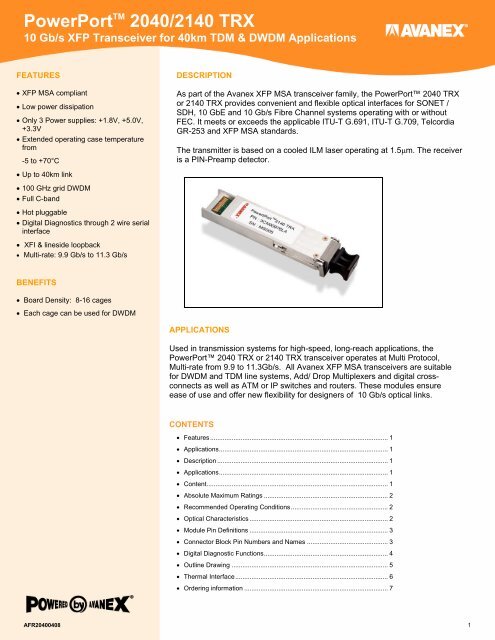
PowerPort TM 20<strong>40</strong>/21<strong>40</strong> TRX<br />
10 <strong>Gb</strong>/s XFP Transceiver for <strong>40</strong>km TDM & DWDM Applications<br />
FEATURES<br />
• XFP MSA compliant<br />
• Low power dissipation<br />
• Only 3 Power supplies: +1.8V, +5.0V,<br />
+3.3V<br />
• Extended operating case temperature<br />
from<br />
-5 to +70°C<br />
• Up to <strong>40</strong>km link<br />
• 100 GHz grid DWDM<br />
• Full C-band<br />
• Hot pluggable<br />
• Digital Diagnostics through 2 wire serial<br />
interface<br />
• XFI & lineside loopback<br />
• Multi-rate: 9.9 <strong>Gb</strong>/s to 11.3 <strong>Gb</strong>/s<br />
BENEFITS<br />
• Board Density: 8-16 cages<br />
• Each cage can be used for DWDM<br />
AFR20<strong>40</strong>0<strong>40</strong>8<br />
DESCRIPTION<br />
As part of the Avanex XFP MSA transceiver family, the PowerPort 20<strong>40</strong> TRX<br />
or 21<strong>40</strong> TRX provides convenient and flexible optical interfaces for SONET /<br />
<strong>SD</strong>H, 10 <strong>Gb</strong>E and 10 <strong>Gb</strong>/s Fibre Channel systems operating with or without<br />
FEC. It meets or exceeds the applicable ITU-T G.691, ITU-T G.709, Telcordia<br />
GR-253 and XFP MSA standards.<br />
The transmitter is based on a cooled ILM laser operating at 1.5µm. The receiver<br />
is a PIN-Preamp detector.<br />
APPLICATIONS<br />
Used in transmission systems for high-speed, long-reach applications, the<br />
PowerPort 20<strong>40</strong> TRX or 21<strong>40</strong> TRX transceiver operates at Multi Protocol,<br />
Multi-rate from 9.9 to 11.3<strong>Gb</strong>/s. All Avanex XFP MSA transceivers are suitable<br />
for DWDM and TDM line systems, Add/ Drop Multiplexers and digital crossconnects<br />
as well as ATM or IP switches and routers. These modules ensure<br />
ease of use and offer new flexibility for designers of 10 <strong>Gb</strong>/s optical links.<br />
C ONTENTS<br />
• Features................................................................................................... 1<br />
• Applications.............................................................................................. 1<br />
• Description ............................................................................................... 1<br />
• Applications.............................................................................................. 1<br />
• Content..................................................................................................... 1<br />
• Absolute Maximum Ratings ..................................................................... 2<br />
• Recommended Operating Conditions...................................................... 2<br />
• Optical Characteristics ............................................................................. 2<br />
• Module Pin Definitions ............................................................................. 3<br />
• Connector Block Pin Numbers and Names ............................................. 3<br />
• Digital Diagnostic Functions..................................................................... 4<br />
• Outline Drawing ....................................................................................... 5<br />
• Thermal Interface..................................................................................... 6<br />
• Ordering information ................................................................................ 7<br />
1
PowerPort TM 20<strong>40</strong>/21<strong>40</strong> TRX<br />
10 <strong>Gb</strong>/s XFP Transceiver for <strong>40</strong>km TDM & DWDM Applications<br />
ABSOLUTE MAXIMUM RATINGS 1<br />
Parameter Symbol Min Max Unit<br />
Optical input Power Damage Threshold +3 dBm<br />
Supply Voltages<br />
Vcc5 0 +6.0 V<br />
Vcc3 0 + 3.6 V<br />
Vcc2 0 +2.0 V<br />
Data AC Voltage Differential Tx+, Tx- 0 +2.0 Vpp<br />
Control Input Voltage 0 Vcc3 V<br />
Storage Temperature TSTG -<strong>40</strong> +85 °C<br />
Note 1: Exposing the device to stresses above those listed in absolute maximum rating could cause permanent damage.<br />
The device is not meant to operate under conditions outside the limits described in the operational sections of this specification.<br />
Exposure to absolute maximum rating conditions for extended periods may adversely affect device reliability.<br />
RECOMENDED OPERATING CONDITIONS<br />
Parameter Symbol Min Typ Max Units<br />
Bit Rate 9.9 11.3 <strong>Gb</strong>/s<br />
Supply Voltage +5V Vcc5 4.75 5.0 5.25 V<br />
Supply Voltage +3.3V Vcc3 3.13 3.3 3.47 V<br />
Supply Voltage 1.8V Vcc2 1.7 1.8 1.89 V<br />
Total Power Dissipation -5 3.5 W<br />
Operating Case Temperature Top +70 °C<br />
OPTICAL CHARACTERISTICS<br />
Conditions Min Typ Max Unit<br />
Target Distance <strong>40</strong> km<br />
Optical Path Penalty Note 2 2 dB<br />
Optical Return Loss (ORL) -27 dB<br />
Parameters 1<br />
Transmitter<br />
Signal Wavelength Range 1529 1563 nm<br />
Over-Lifetime Wavelength Stability -100 +100 pm<br />
Output Power -1 +2 dB<br />
Side Mode Suppression Ratio 30 dB<br />
Extinction Ratio Note 3 9 dB<br />
Return loss 24 dB<br />
Jitter Generation Note 4 Compliant with<br />
GR 253 Issue 3<br />
Receiver<br />
Receiver Sensitivity Note 5 -16 -14 dB<br />
Receiver Overload -1 dB<br />
Reflectance -27 dB<br />
Note 1: Minimum and maximum parameters are specified End-of-Life within the overall relevant operating temperature range<br />
unless otherwise stated. Typical values are referenced to +25 °C, nominal power supply, beginning of life. Optical<br />
characteristics are guaranteed with up to –24dB line optical return loss.<br />
Note 2: For Tx/Rx pair, penalty includes chromatic dispersion, PMD, reflections, and jitter effects and an OSNR >30dB. There<br />
is an additional penalty for lower OSNR.<br />
Note 3: Measured @BER 10 -12 and under modulation conditions NRZ at 9.953 <strong>Gb</strong>/s and PRBS 2 23 -1.<br />
Note 4: Measured in accordance with the XFP MSA Rev. 4.5.<br />
Note 5: Measured @BER 10 -12 and under modulation conditions NRZ at 9.953 <strong>Gb</strong>/s and PRBS 2 23 -1.<br />
AFR20<strong>40</strong>0<strong>40</strong>8 2
PowerPort TM 20<strong>40</strong>/21<strong>40</strong> TRX<br />
10 <strong>Gb</strong>/s XFP Transceiver for <strong>40</strong>km TDM & DWDM Applications<br />
MODULE PIN DEFINITIONS<br />
Pin Logic Symbol Name/Description Note<br />
1, 7, 15 , 16, 19,<br />
23, 26, 27, 30<br />
GND Module Ground 1<br />
3 LVTTL-I Mod_DeSel<br />
Module De-select; When jeld low allows module to respond to 2wire<br />
inteface<br />
3<br />
4 LVTTL-O Interrupt<br />
Interrupt; Indicates presence of an important condition which can<br />
be read over the 2-wire serial interface<br />
2<br />
5 LVTTL-I TX_DIS Transmitter Disable; Turns off transmitter laser output<br />
6 Vcc5 + 5V power supply<br />
8,9 Vcc3 + 3.3V power supply<br />
10 LVTTL-I/O SCL 2-Wire Serial Interface Clock 2<br />
11 LVTTL-I/O <strong>SD</strong>A 2-Wire Serial Interface Data Line 2<br />
12 LVTTL-O Mod_Abs Indicates Module is not present. Grounded in the Module 2<br />
13 LVTTL-O Mod_NR Nodule Not Ready; Indicating Module Operational Fault 2<br />
14 LVTTL-O RX_LOS Receiver Loss of Signal Indicator 2<br />
17 CML-0 RD- Receiver Inverted Data Output<br />
18 CML-0 RD+ Receiver Non-Inverted Data Output<br />
20,22 Vcc2 + 1.8V power supply<br />
Power down; When high, requires the module to limit power<br />
consumption to 1.5W or below. 2-Wire serial interface must be<br />
21 LVTTL-I P_Down/RST functional in the low power mode.<br />
Reset; The falling edge initiates a complete reset of the moduel<br />
including the 2-wire serial interface, equivalent to a power cycle.<br />
24 PECL-I RefCLK+<br />
Reference Clock Non-Inverted Input, AC coupled on the host<br />
board<br />
4<br />
25 PECL-I RefCLK- Reference Clock Inverted Input, AC coupled on the host board 4<br />
28 CML-I TD- Transmitter Inverted Data Input<br />
29 CML-I TD+ Transmitter Non-Inverted Data Input<br />
Note 1. Module ground pins Gnd are isolated from the module case and chassis ground within the module<br />
Note 2. Pulled up with 4.7 – 10Kohms to a voltage between 3.15V and 3.45V on the host board<br />
Note 3. The negative power supply (–5.2V) is not required<br />
Note 4. Reference clock is required<br />
CONNECTOR BLOCK PIN NAMES<br />
16 GND<br />
17 RD-<br />
18 RD+<br />
19 GND<br />
20 VCC2<br />
21 P_DOWN / RST<br />
22 VCC2<br />
GND 15<br />
RX_LOS 14<br />
MOD_NR 13<br />
MOD_ABS 12<br />
<strong>SD</strong>A 11<br />
SCL 10<br />
VCC3 9<br />
Toward VCC3 8 Toward<br />
ASIC 23 GND Bezel<br />
24 REFCLK+<br />
25 REFCLK-<br />
26 GND<br />
27 GND<br />
28 TD-<br />
29 TD+<br />
30 GND<br />
GND 7<br />
VCC5 6<br />
TX_DIS 5<br />
INTERRUPT 4<br />
MOD_DESEL 3<br />
VEE5 2<br />
GND 1<br />
AFR20<strong>40</strong>0<strong>40</strong>8 3
PowerPort TM 20<strong>40</strong>/21<strong>40</strong> TRX<br />
10 <strong>Gb</strong>/s XFP Transceiver for <strong>40</strong>km TDM & DWDM Applications<br />
DIGITAL DIAGNOSTIC FUNCTIONS<br />
The Avanex XFP module provides a management interface as described in the XFP standard (MSA Rev 4.5). There are<br />
3 control input signals, 3 status output signals, and a 2-wire serial interface. The signals are described in section 2.4 of the<br />
XFP standard. The control signals allow the module to be placed in a low-power state, to be reset, to enable/disable the<br />
serial interface, and to turn-off the transmitter. The status signals indicate loss of received signal, detection of an invalid<br />
condition, and the presence of additional status information via the serial interface.<br />
The serial interface provides access to the more detailed identification and diagnostic monitoring information. It provides<br />
access to a 256-byte register space. This interface runs at up to <strong>40</strong>0 kHz (with occasional clock stretching not exceeding<br />
500µs), and the module supports a packet error checking protocol to verify transfer integrity. Full details are described in<br />
chapter 4 of the XFP standard.<br />
The register space is divided into upper and lower 128-byte spaces, as described in chapter 5 of the standard. The lower<br />
128-bytes provides access to the more frequently accessed information, including readout of optical signal and laser<br />
levels, alarm and warning flags, and read/write of control and status signals. The upper 128-bytes contain one of a<br />
number of pages of information. The desired page is selected by writing a byte in the lower 128-half. Page 1 contains<br />
extended module identification information, and page 2 provides a space of 128-bytes of non-volatile storage for the host<br />
system.<br />
In order to accommodate the signal conditioner device used in our XFP module, the host system shall inform the XFP<br />
module of the data rate. The data rate is written into the upper 4 bits [7-4] of Byte 01h. The value to be entered is given<br />
by:<br />
Byte 01h [bits 7-4] = INT(Data rate[<strong>Gb</strong>ps) – 9.5 ) /0.2))<br />
Table below gives Byte 01h [bits 7-4] depending on the data rate used:<br />
AFR20<strong>40</strong><strong>40</strong>8<br />
Error Correcting Capapility<br />
Percentage<br />
Bandwidth<br />
Expansion Data Rate<br />
Required<br />
REFCLK<br />
Frequency<br />
Byte<br />
01h[bits7-4]<br />
STS-192, 0 bytes 0% 9.953 <strong>Gb</strong>ps 155.52 MHz 0010xxxx<br />
10 Gigabit Ethernet 0% 10 <strong>Gb</strong>ps 156.25 MHz 0010xxxx<br />
10 Gigabit Ethernet 64/66B<br />
encoded 3,125% 10.3125 <strong>Gb</strong>ps 161.13 MHz 0100xxxx<br />
10 G Fiber Channel 0% 10.5187 <strong>Gb</strong>ps 164.35 MHz 0101xxxx<br />
STS-192, Reed Solomon -<br />
255/238 7,14% 10.66 <strong>Gb</strong>ps 166.63 MHz 0101xxxx<br />
STS-192, Reed Solomon -<br />
255/237 7,59% 10.709 <strong>Gb</strong>ps 167.33 MHz 0110xxxx<br />
10 Gigabit Ethernet 64/66B<br />
encoded - 255/238 7,14% 11.0491 <strong>Gb</strong>ps 172.642 MHz 0111xxxx<br />
g<br />
encoded - 255/237 7,59% 11.0957 <strong>Gb</strong>ps 173.37 MHz 0111xxxx<br />
10 G Fiber Channel, Reed<br />
Solomon -255/238 7,14% 11.27 <strong>Gb</strong>ps 176.095 MHz 1000xxxx<br />
10 G Fiber Channel, Reed<br />
Solomon -255/237 7,59% 11.318 <strong>Gb</strong>ps 176.84 MHz 1001xxxx<br />
4
PowerPort TM 20<strong>40</strong>/21<strong>40</strong> TRX<br />
10 <strong>Gb</strong>/s XFP Transceiver for <strong>40</strong>km TDM & DWDM Applications<br />
OUTLINE DRAWING<br />
THERMAL INTERFACE<br />
The XFP module cage is designed to accommodate a clip-on thermal heat sink, as shown below, to enhance the<br />
cooling of the module. Thus the equipment manufacturer can select a heat sink that is optimized for the particular<br />
environmental conditions of space-above-module, air flow rate & direction. For an example reference of the heat sink,<br />
see Tyco, ref. 1542706-2.<br />
LATCHED<br />
UNLATCHED<br />
AFR20<strong>40</strong>0<strong>40</strong>8 8<br />
7 6 5
PowerPort TM 20<strong>40</strong>/21<strong>40</strong> TRX<br />
10 <strong>Gb</strong>/s XFP Transceiver for <strong>40</strong>km TDM & DWDM Applications<br />
ORDERING INFORMATION<br />
PowerPort 20<strong>40</strong> TRX, Black and White TDM version:<br />
Type Dispersion Part Number Connector<br />
I-64.3II-64.2 <strong>40</strong>km 1<br />
3CN05003AB LC<br />
Note 1: Dispersion measured with ITU-T G.652 fiber.<br />
PowerPort 21<strong>40</strong> TRX, DWDM version:<br />
Type Dispersion Part Number Connector<br />
WDM <strong>40</strong>km 1<br />
3CN05035yy LC<br />
Note 1: Dispersion measured with ITU-T G.652 fiber.<br />
WAVELENGTH OPTIONS (YY)<br />
AFL80800<strong>40</strong>8<br />
CH CH CH CH<br />
yy (THz) (nm) yy (THz) (nm)<br />
NJ 191.8 1 563.05 JS 194 1 545.32<br />
NE 191.9 1 562.23 JN 194.1 1 544.53<br />
NA 192 1 561.42 JJ 194.2 1 543.73<br />
MW 192.1 1 560.61 JE 194.3 1 542.94<br />
MS 192.2 1 559.79 JA 194.4 1 542.14<br />
MN 192.3 1 558.98 HW 194.5 1 541.35<br />
MJ 192.4 1 558.17 HS 194.6 1 5<strong>40</strong>.56<br />
ME 192.5 1 557.36 HN 194.7 1 539.77<br />
MA 192.6 1 556.55 HJ 194.8 1 538.98<br />
LW 192.7 1 555.75 HE 194.9 1 538.19<br />
LS 192.8 1 554.94 HA 195 1 537.<strong>40</strong><br />
LN 192.9 1 554.13 GW 195.1 1 536.61<br />
LJ 193 1 553.33 GS 195.2 1 535.82<br />
LE 193.1 1 552.52 GN 195.3 1 535.04<br />
LA 193.2 1 551.72 GJ 195.4 1 534.25<br />
KW 193.3 1 550.92 GE 195.5 1 533.47<br />
KS 193.4 1 550.12 GA 195.6 1 532.68<br />
KN 193.5 1 549.32 FW 195.7 1 531.90<br />
KJ 193.6 1 548.51 FS 195.8 1 531.12<br />
KE 193.7 1 547.72 FN 195.9 1 530.33<br />
KA 193.8 1 546.92 FJ 196 1 529.55<br />
JW 193.9 1 546.12 FE 196.1 1 528.77<br />
Performance figures contained in this document must be specifically<br />
confirmed in writing by Avanex before they become applicable to any<br />
particular order or contract. Avanex reserves the right to make changes to<br />
the products or information contained herein without notice.<br />
For additional information, contact your Avanex Account Manager or<br />
request information through our website at:<br />
http://www.avanex.com/Contactus/requestinfo.html<br />
<strong>40</strong>919 Encyclopedia Circle Fremont, CA 94538 USA • Telephone 510-897-4188 • Fax 510-897-4189<br />
©2008 Avanex Corporation. Actual data will vary according to the specific product and the specific application.<br />
10