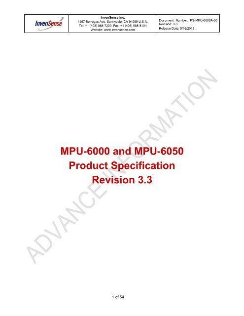
MPU-6000 and MPU-6050 Product Specification ... - InvenSense
MPU-6000 and MPU-6050 Product Specification ... - InvenSense
MPU-6000 and MPU-6050 Product Specification ... - InvenSense

Create successful ePaper yourself
Turn your PDF publications into a flip-book with our unique Google optimized e-Paper software.
<strong>InvenSense</strong> Inc.<br />
1197 Borregas Ave, Sunnyvale, CA 94089 U.S.A.<br />
Tel: +1 (408) 988-7339 Fax: +1 (408) 988-8104<br />
Website: www.invensense.com<br />
<strong>MPU</strong>-<strong>6000</strong> <strong>and</strong> <strong>MPU</strong>-<strong>6050</strong><br />
<strong>Product</strong> <strong>Specification</strong><br />
Revision 3.3<br />
1 of 54<br />
Document Number: PS-<strong>MPU</strong>-<strong>6000</strong>A-00<br />
Revision: 3.3<br />
Release Date: 5/16/2012
CONTENTS<br />
<strong>MPU</strong>-<strong>6000</strong>/<strong>MPU</strong>-<strong>6050</strong> <strong>Product</strong> <strong>Specification</strong><br />
2 of 54<br />
Document Number: PS-<strong>MPU</strong>-<strong>6000</strong>A-00<br />
Revision: 3.3<br />
Release Date: 5/16/2012<br />
1 REVISION HISTORY ................................................................................................................................... 5<br />
2 PURPOSE AND SCOPE ............................................................................................................................. 6<br />
3 PRODUCT OVERVIEW ............................................................................................................................... 7<br />
3.1 <strong>MPU</strong>-60X0 OVERVIEW ........................................................................................................................ 7<br />
4 APPLICATIONS ........................................................................................................................................... 9<br />
5 FEATURES ................................................................................................................................................ 10<br />
5.1 GYROSCOPE FEATURES ..................................................................................................................... 10<br />
5.2 ACCELEROMETER FEATURES ............................................................................................................. 10<br />
5.3 ADDITIONAL FEATURES ...................................................................................................................... 10<br />
5.4 MOTIONPROCESSING ......................................................................................................................... 11<br />
5.5 CLOCKING ......................................................................................................................................... 11<br />
6 ELECTRICAL CHARACTERISTICS ......................................................................................................... 12<br />
6.1 GYROSCOPE SPECIFICATIONS ............................................................................................................ 12<br />
6.2 ACCELEROMETER SPECIFICATIONS ..................................................................................................... 13<br />
6.3 ELECTRICAL AND OTHER COMMON SPECIFICATIONS ............................................................................ 14<br />
6.4 ELECTRICAL SPECIFICATIONS, CONTINUED ......................................................................................... 15<br />
6.5 ELECTRICAL SPECIFICATIONS, CONTINUED ......................................................................................... 16<br />
6.6 ELECTRICAL SPECIFICATIONS, CONTINUED ......................................................................................... 17<br />
6.7 I 2 C TIMING CHARACTERIZATION.......................................................................................................... 18<br />
6.8 SPI TIMING CHARACTERIZATION (<strong>MPU</strong>-<strong>6000</strong> ONLY) ........................................................................... 19<br />
6.9 ABSOLUTE MAXIMUM RATINGS ........................................................................................................... 20<br />
7 APPLICATIONS INFORMATION .............................................................................................................. 21<br />
7.1 PIN OUT AND SIGNAL DESCRIPTION .................................................................................................... 21<br />
7.2 TYPICAL OPERATING CIRCUIT ............................................................................................................. 22<br />
7.3 BILL OF MATERIALS FOR EXTERNAL COMPONENTS .............................................................................. 22<br />
7.4 RECOMMENDED POWER-ON PROCEDURE ........................................................................................... 23<br />
7.5 BLOCK DIAGRAM ............................................................................................................................... 24<br />
7.6 OVERVIEW ........................................................................................................................................ 24<br />
7.7 THREE-AXIS MEMS GYROSCOPE WITH 16-BIT ADCS AND SIGNAL CONDITIONING ................................ 25<br />
7.8 THREE-AXIS MEMS ACCELEROMETER WITH 16-BIT ADCS AND SIGNAL CONDITIONING ........................ 25<br />
7.9 DIGITAL MOTION PROCESSOR ............................................................................................................ 25<br />
7.10 PRIMARY I 2 C AND SPI SERIAL COMMUNICATIONS INTERFACES ............................................................ 25<br />
7.11 AUXILIARY I 2 C SERIAL INTERFACE ...................................................................................................... 26
<strong>MPU</strong>-<strong>6000</strong>/<strong>MPU</strong>-<strong>6050</strong> <strong>Product</strong> <strong>Specification</strong><br />
3 of 54<br />
Document Number: PS-<strong>MPU</strong>-<strong>6000</strong>A-00<br />
Revision: 3.3<br />
Release Date: 5/16/2012<br />
7.12 SELF-TEST ........................................................................................................................................ 27<br />
7.13 <strong>MPU</strong>-60X0 SOLUTION FOR 9-AXIS SENSOR FUSION USING I 2 C INTERFACE .......................................... 28<br />
7.14 <strong>MPU</strong>-<strong>6000</strong> USING SPI INTERFACE ..................................................................................................... 29<br />
7.15 INTERNAL CLOCK GENERATION .......................................................................................................... 30<br />
7.16 SENSOR DATA REGISTERS ................................................................................................................. 30<br />
7.17 FIFO ................................................................................................................................................ 30<br />
7.18 INTERRUPTS ...................................................................................................................................... 30<br />
7.19 DIGITAL-OUTPUT TEMPERATURE SENSOR .......................................................................................... 31<br />
7.20 BIAS AND LDO .................................................................................................................................. 31<br />
7.21 CHARGE PUMP .................................................................................................................................. 31<br />
8 PROGRAMMABLE INTERRUPTS ............................................................................................................ 32<br />
8.1 MOTION INTERRUPT ........................................................................................................................... 33<br />
9 DIGITAL INTERFACE ............................................................................................................................... 34<br />
9.1 I 2 C AND SPI (<strong>MPU</strong>-<strong>6000</strong> ONLY) SERIAL INTERFACES .......................................................................... 34<br />
9.2 I 2 C INTERFACE .................................................................................................................................. 34<br />
9.3 I 2 C COMMUNICATIONS PROTOCOL ...................................................................................................... 34<br />
9.4 I 2 C TERMS ........................................................................................................................................ 37<br />
9.5 SPI INTERFACE (<strong>MPU</strong>-<strong>6000</strong> ONLY) .................................................................................................... 38<br />
10 SERIAL INTERFACE CONSIDERATIONS (<strong>MPU</strong>-<strong>6050</strong>) .......................................................................... 39<br />
10.1 <strong>MPU</strong>-<strong>6050</strong> SUPPORTED INTERFACES ................................................................................................. 39<br />
10.2 LOGIC LEVELS ................................................................................................................................... 39<br />
10.3 LOGIC LEVELS DIAGRAM FOR AUX_VDDIO = 0 .................................................................................. 40<br />
10.4 LOGIC LEVELS DIAGRAM FOR AUX_VDDIO = 1 .................................................................................. 41<br />
11 ASSEMBLY ............................................................................................................................................... 42<br />
11.1 ORIENTATION OF AXES ...................................................................................................................... 42<br />
11.2 PACKAGE DIMENSIONS ...................................................................................................................... 43<br />
11.3 PCB DESIGN GUIDELINES .................................................................................................................. 44<br />
11.4 ASSEMBLY PRECAUTIONS .................................................................................................................. 45<br />
11.5 STORAGE SPECIFICATIONS ................................................................................................................. 48<br />
11.6 PACKAGE MARKING SPECIFICATION .................................................................................................... 48<br />
11.7 TAPE & REEL SPECIFICATION ............................................................................................................. 49<br />
11.8 LABEL ............................................................................................................................................... 50<br />
11.9 PACKAGING ....................................................................................................................................... 51<br />
11.10 REPRESENTATIVE SHIPPING CARTON LABEL ................................................................................... 52
<strong>MPU</strong>-<strong>6000</strong>/<strong>MPU</strong>-<strong>6050</strong> <strong>Product</strong> <strong>Specification</strong><br />
4 of 54<br />
Document Number: PS-<strong>MPU</strong>-<strong>6000</strong>A-00<br />
Revision: 3.3<br />
Release Date: 5/16/2012<br />
12 RELIABILITY ............................................................................................................................................. 53<br />
12.1 QUALIFICATION TEST POLICY ............................................................................................................. 53<br />
12.2 QUALIFICATION TEST PLAN ................................................................................................................ 53<br />
13 ENVIRONMENTAL COMPLIANCE ........................................................................................................... 54
1 Revision History<br />
Revision<br />
Date<br />
<strong>MPU</strong>-<strong>6000</strong>/<strong>MPU</strong>-<strong>6050</strong> <strong>Product</strong> <strong>Specification</strong><br />
Revision Description<br />
11/24/2010 1.0 Initial Release<br />
05/19/2011 2.0<br />
5 of 54<br />
Document Number: PS-<strong>MPU</strong>-<strong>6000</strong>A-00<br />
Revision: 3.3<br />
Release Date: 5/16/2012<br />
For Rev C parts. Clarified wording in sections (3.2, 5.1, 5.2, 6.1-6.4, 6.6, 6.9, 7,<br />
7.1-7.6, 7.11, 7.12, 7.14, 8, 8.2-8.4, 10.3, 10.4, 11, 12.2)<br />
07/28/2011 2.1 Edited supply current numbers for different modes (section 6.4)<br />
08/05/2011 2.2 Unit of measure for accelerometer sensitivity changed from LSB/mg to LSB/g<br />
10/12/2011 2.3<br />
10/18/2011 3.0<br />
10/24/2011 3.1<br />
11/16/2011 3.2<br />
5/16/2012 3.3<br />
Updated accelerometer self test specifications in Table 6.2. Updated package<br />
dimensions (section 11.2). Updated PCB design guidelines (section 11.3)<br />
For Rev D parts. Updated accelerometer specifications in Table 6.2. Updated<br />
accelerometer specification note (sections 8.2, 8.3, & 8.4). Updated qualification<br />
test plan (section 12.2).<br />
Edits for clarity<br />
Changed operating voltage range to 2.375V-3.46V<br />
Added accelerometer Intelligence Function increment value of 1mg/LSB<br />
(Section 6.2)<br />
Updated absolute maximum rating for acceleration (any axis, unpowered) from<br />
0.3ms to 0.2ms (Section 6.9)<br />
Modified absolute maximum rating for Latch-up to Level A <strong>and</strong> ±100mA (Section<br />
6.9, 12.2)<br />
Updated self-test response specifications for Revision D parts dated with<br />
date code 1147 (YYWW) or later.<br />
Edits for clarity<br />
Added Gyro self-test (sections 5.1, 6.1, 7.6, 7.12)<br />
Added Min/Max limits to Accel self-test response (section 6.2)<br />
Updated Accelerometer low power mode operating currents (Section 6.3)<br />
Added gyro self test to block diagram (section 7.5)<br />
Updated packaging labels <strong>and</strong> descriptions (sections 11.8 & 11.9)<br />
Updated Gyro <strong>and</strong> Accelerometer self test information (sections 6.1, 6.2, 7.12)<br />
Updated latch-up information (Section 6.9)<br />
Updated programmable interrupts information (Section 8)<br />
Changed shipment information from maximum of 3 reels (15K units) per shipper<br />
box to 5 reels (25K units) per shipper box (Section 11.7)<br />
Updated packing shipping <strong>and</strong> label information (Sections 11.8, 11.9)<br />
Updated reliability references (Section 12.2)
2 Purpose <strong>and</strong> Scope<br />
<strong>MPU</strong>-<strong>6000</strong>/<strong>MPU</strong>-<strong>6050</strong> <strong>Product</strong> <strong>Specification</strong><br />
6 of 54<br />
Document Number: PS-<strong>MPU</strong>-<strong>6000</strong>A-00<br />
Revision: 3.3<br />
Release Date: 5/16/2012<br />
This product specification provides advanced information regarding the electrical specification <strong>and</strong> design<br />
related information for the <strong>MPU</strong>-<strong>6000</strong> <strong>and</strong> <strong>MPU</strong>-<strong>6050</strong> MotionTracking devices, collectively called the<br />
<strong>MPU</strong>-60X0 or <strong>MPU</strong>.<br />
Electrical characteristics are based upon design analysis <strong>and</strong> simulation results only. <strong>Specification</strong>s are<br />
subject to change without notice. Final specifications will be updated based upon characterization of<br />
production silicon. For references to register map <strong>and</strong> descriptions of individual registers, please refer to the<br />
<strong>MPU</strong>-<strong>6000</strong>/<strong>MPU</strong>-<strong>6050</strong> Register Map <strong>and</strong> Register Descriptions document.<br />
The self-test response specifications provided in this document pertain to Revision D parts with date<br />
codes of 1147 (YYWW) or later. Please see Section 11.6 for package marking description details.
3 <strong>Product</strong> Overview<br />
<strong>MPU</strong>-<strong>6000</strong>/<strong>MPU</strong>-<strong>6050</strong> <strong>Product</strong> <strong>Specification</strong><br />
7 of 54<br />
Document Number: PS-<strong>MPU</strong>-<strong>6000</strong>A-00<br />
Revision: 3.3<br />
Release Date: 5/16/2012<br />
3.1 <strong>MPU</strong>-60X0 Overview<br />
MotionInterface is becoming a “must-have” function being adopted by smartphone <strong>and</strong> tablet<br />
manufacturers due to the enormous value it adds to the end user experience. In smartphones, it finds use in<br />
applications such as gesture comm<strong>and</strong>s for applications <strong>and</strong> phone control, enhanced gaming, augmented<br />
reality, panoramic photo capture <strong>and</strong> viewing, <strong>and</strong> pedestrian <strong>and</strong> vehicle navigation. With its ability to<br />
precisely <strong>and</strong> accurately track user motions, MotionTracking technology can convert h<strong>and</strong>sets <strong>and</strong> tablets<br />
into powerful 3D intelligent devices that can be used in applications ranging from health <strong>and</strong> fitness<br />
monitoring to location-based services. Key requirements for MotionInterface enabled devices are small<br />
package size, low power consumption, high accuracy <strong>and</strong> repeatability, high shock tolerance, <strong>and</strong> application<br />
specific performance programmability – all at a low consumer price point.<br />
The <strong>MPU</strong>-60X0 is the world’s first integrated 6-axis MotionTracking device that combines a 3-axis<br />
gyroscope, 3-axis accelerometer, <strong>and</strong> a Digital Motion Processor (DMP) all in a small 4x4x0.9mm<br />
package. With its dedicated I 2 C sensor bus, it directly accepts inputs from an external 3-axis compass to<br />
provide a complete 9-axis MotionFusion output. The <strong>MPU</strong>-60X0 MotionTracking device, with its 6-axis<br />
integration, on-board MotionFusion, <strong>and</strong> run-time calibration firmware, enables manufacturers to eliminate<br />
the costly <strong>and</strong> complex selection, qualification, <strong>and</strong> system level integration of discrete devices, guaranteeing<br />
optimal motion performance for consumers. The <strong>MPU</strong>-60X0 is also designed to interface with multiple noninertial<br />
digital sensors, such as pressure sensors, on its auxiliary I 2 C port. The <strong>MPU</strong>-60X0 is footprint<br />
compatible with the <strong>MPU</strong>-30X0 family.<br />
The <strong>MPU</strong>-60X0 features three 16-bit analog-to-digital converters (ADCs) for digitizing the gyroscope outputs<br />
<strong>and</strong> three 16-bit ADCs for digitizing the accelerometer outputs. For precision tracking of both fast <strong>and</strong> slow<br />
motions, the parts feature a user-programmable gyroscope full-scale range of ±250, ±500, ±1000, <strong>and</strong><br />
±2000°/sec (dps) <strong>and</strong> a user-programmable accelerometer full-scale range of ±2g, ±4g, ±8g, <strong>and</strong> ±16g.<br />
An on-chip 1024 Byte FIFO buffer helps lower system power consumption by allowing the system processor<br />
to read the sensor data in bursts <strong>and</strong> then enter a low-power mode as the <strong>MPU</strong> collects more data. With all<br />
the necessary on-chip processing <strong>and</strong> sensor components required to support many motion-based use<br />
cases, the <strong>MPU</strong>-60X0 uniquely enables low-power MotionInterface applications in portable applications with<br />
reduced processing requirements for the system processor. By providing an integrated MotionFusion output,<br />
the DMP in the <strong>MPU</strong>-60X0 offloads the intensive MotionProcessing computation requirements from the<br />
system processor, minimizing the need for frequent polling of the motion sensor output.<br />
Communication with all registers of the device is performed using either I 2 C at 400kHz or SPI at 1MHz<br />
(<strong>MPU</strong>-<strong>6000</strong> only). For applications requiring faster communications, the sensor <strong>and</strong> interrupt registers may<br />
be read using SPI at 20MHz (<strong>MPU</strong>-<strong>6000</strong> only). Additional features include an embedded temperature sensor<br />
<strong>and</strong> an on-chip oscillator with ±1% variation over the operating temperature range.<br />
By leveraging its patented <strong>and</strong> volume-proven Nasiri-Fabrication platform, which integrates MEMS wafers<br />
with companion CMOS electronics through wafer-level bonding, <strong>InvenSense</strong> has driven the <strong>MPU</strong>-60X0<br />
package size down to a revolutionary footprint of 4x4x0.9mm (QFN), while providing the highest<br />
performance, lowest noise, <strong>and</strong> the lowest cost semiconductor packaging required for h<strong>and</strong>held consumer<br />
electronic devices. The part features a robust 10,000g shock tolerance, <strong>and</strong> has programmable low-pass<br />
filters for the gyroscopes, accelerometers, <strong>and</strong> the on-chip temperature sensor.<br />
For power supply flexibility, the <strong>MPU</strong>-60X0 operates from VDD power supply voltage range of 2.375V-3.46V.<br />
Additionally, the <strong>MPU</strong>-<strong>6050</strong> provides a VLOGIC reference pin (in addition to its analog supply pin: VDD),<br />
which sets the logic levels of its I 2 C interface. The VLOGIC voltage may be 1.8V±5% or VDD.<br />
The <strong>MPU</strong>-<strong>6000</strong> <strong>and</strong> <strong>MPU</strong>-<strong>6050</strong> are identical, except that the <strong>MPU</strong>-<strong>6050</strong> supports the I 2 C serial interface only,<br />
<strong>and</strong> has a separate VLOGIC reference pin. The <strong>MPU</strong>-<strong>6000</strong> supports both I 2 C <strong>and</strong> SPI interfaces <strong>and</strong> has a<br />
single supply pin, VDD, which is both the device’s logic reference supply <strong>and</strong> the analog supply for the part.<br />
The table below outlines these differences:
<strong>MPU</strong>-<strong>6000</strong>/<strong>MPU</strong>-<strong>6050</strong> <strong>Product</strong> <strong>Specification</strong><br />
Primary Differences between <strong>MPU</strong>-<strong>6000</strong> <strong>and</strong> <strong>MPU</strong>-<strong>6050</strong><br />
8 of 54<br />
Document Number: PS-<strong>MPU</strong>-<strong>6000</strong>A-00<br />
Revision: 3.3<br />
Release Date: 5/16/2012<br />
Part / Item <strong>MPU</strong>-<strong>6000</strong> <strong>MPU</strong>-<strong>6050</strong><br />
VDD 2.375V-3.46V 2.375V-3.46V<br />
VLOGIC n/a 1.71V to VDD<br />
Serial Interfaces Supported I 2 C, SPI I 2 C<br />
Pin 8 /CS VLOGIC<br />
Pin 9 AD0/SDO AD0<br />
Pin 23 SCL/SCLK SCL<br />
Pin 24 SDA/SDI SDA
4 Applications<br />
<strong>MPU</strong>-<strong>6000</strong>/<strong>MPU</strong>-<strong>6050</strong> <strong>Product</strong> <strong>Specification</strong><br />
� BlurFree technology (for Video/Still Image Stabilization)<br />
� AirSign technology (for Security/Authentication)<br />
� TouchAnywhere technology (for “no touch” UI Application Control/Navigation)<br />
� MotionComm<strong>and</strong> technology (for Gesture Short-cuts)<br />
� Motion-enabled game <strong>and</strong> application framework<br />
� InstantGesture iG gesture recognition<br />
� Location based services, points of interest, <strong>and</strong> dead reckoning<br />
� H<strong>and</strong>set <strong>and</strong> portable gaming<br />
� Motion-based game controllers<br />
� 3D remote controls for Internet connected DTVs <strong>and</strong> set top boxes, 3D mice<br />
� Wearable sensors for health, fitness <strong>and</strong> sports<br />
� Toys<br />
9 of 54<br />
Document Number: PS-<strong>MPU</strong>-<strong>6000</strong>A-00<br />
Revision: 3.3<br />
Release Date: 5/16/2012
5 Features<br />
<strong>MPU</strong>-<strong>6000</strong>/<strong>MPU</strong>-<strong>6050</strong> <strong>Product</strong> <strong>Specification</strong><br />
5.1 Gyroscope Features<br />
The triple-axis MEMS gyroscope in the <strong>MPU</strong>-60X0 includes a wide range of features:<br />
10 of 54<br />
Document Number: PS-<strong>MPU</strong>-<strong>6000</strong>A-00<br />
Revision: 3.3<br />
Release Date: 5/16/2012<br />
� Digital-output X-, Y-, <strong>and</strong> Z-Axis angular rate sensors (gyroscopes) with a user-programmable fullscale<br />
range of ±250, ±500, ±1000, <strong>and</strong> ±2000°/sec<br />
� External sync signal connected to the FSYNC pin supports image, video <strong>and</strong> GPS synchronization<br />
� Integrated 16-bit ADCs enable simultaneous sampling of gyros<br />
� Enhanced bias <strong>and</strong> sensitivity temperature stability reduces the need for user calibration<br />
� Improved low-frequency noise performance<br />
� Digitally-programmable low-pass filter<br />
� Gyroscope operating current: 3.6mA<br />
� St<strong>and</strong>by current: 5µA<br />
� Factory calibrated sensitivity scale factor<br />
� User self-test<br />
5.2 Accelerometer Features<br />
The triple-axis MEMS accelerometer in <strong>MPU</strong>-60X0 includes a wide range of features:<br />
� Digital-output triple-axis accelerometer with a programmable full scale range of ±2g, ±4g, ±8g <strong>and</strong><br />
±16g<br />
� Integrated 16-bit ADCs enable simultaneous sampling of accelerometers while requiring no external<br />
multiplexer<br />
� Accelerometer normal operating current: 500µA<br />
� Low power accelerometer mode current: 10µA at 1.25Hz, 20µA at 5Hz, 60µA at 20Hz, 110µA at<br />
40Hz<br />
� Orientation detection <strong>and</strong> signaling<br />
� Tap detection<br />
� User-programmable interrupts<br />
� High-G interrupt<br />
� User self-test<br />
5.3 Additional Features<br />
The <strong>MPU</strong>-60X0 includes the following additional features:<br />
� 9-Axis MotionFusion by the on-chip Digital Motion Processor (DMP)<br />
� Auxiliary master I 2 C bus for reading data from external sensors (e.g., magnetometer)<br />
� 3.9mA operating current when all 6 motion sensing axes <strong>and</strong> the DMP are enabled<br />
� VDD supply voltage range of 2.375V-3.46V<br />
� Flexible VLOGIC reference voltage supports multiple I 2 C interface voltages (<strong>MPU</strong>-<strong>6050</strong> only)<br />
� Smallest <strong>and</strong> thinnest QFN package for portable devices: 4x4x0.9mm<br />
� Minimal cross-axis sensitivity between the accelerometer <strong>and</strong> gyroscope axes<br />
� 1024 byte FIFO buffer reduces power consumption by allowing host processor to read the data in<br />
bursts <strong>and</strong> then go into a low-power mode as the <strong>MPU</strong> collects more data<br />
� Digital-output temperature sensor<br />
� User-programmable digital filters for gyroscope, accelerometer, <strong>and</strong> temp sensor<br />
� 10,000 g shock tolerant<br />
� 400kHz Fast Mode I 2 C for communicating with all registers<br />
� 1MHz SPI serial interface for communicating with all registers (<strong>MPU</strong>-<strong>6000</strong> only)<br />
� 20MHz SPI serial interface for reading sensor <strong>and</strong> interrupt registers (<strong>MPU</strong>-<strong>6000</strong> only)
<strong>MPU</strong>-<strong>6000</strong>/<strong>MPU</strong>-<strong>6050</strong> <strong>Product</strong> <strong>Specification</strong><br />
� MEMS structure hermetically sealed <strong>and</strong> bonded at wafer level<br />
� RoHS <strong>and</strong> Green compliant<br />
11 of 54<br />
Document Number: PS-<strong>MPU</strong>-<strong>6000</strong>A-00<br />
Revision: 3.3<br />
Release Date: 5/16/2012<br />
5.4 MotionProcessing<br />
� Internal Digital Motion Processing (DMP) engine supports 3D MotionProcessing <strong>and</strong> gesture<br />
recognition algorithms<br />
� The <strong>MPU</strong>-60X0 collects gyroscope <strong>and</strong> accelerometer data while synchronizing data sampling at a<br />
user defined rate. The total dataset obtained by the <strong>MPU</strong>-60X0 includes 3-Axis gyroscope data, 3-<br />
Axis accelerometer data, <strong>and</strong> temperature data. The <strong>MPU</strong>’s calculated output to the system<br />
processor can also include heading data from a digital 3-axis third party magnetometer.<br />
� The FIFO buffers the complete data set, reducing timing requirements on the system processor by<br />
allowing the processor burst read the FIFO data. After burst reading the FIFO data, the system<br />
processor can save power by entering a low-power sleep mode while the <strong>MPU</strong> collects more data.<br />
� Programmable interrupt supports features such as gesture recognition, panning, zooming, scrolling,<br />
zero-motion detection, tap detection, <strong>and</strong> shake detection<br />
� Digitally-programmable low-pass filters<br />
� Low-power pedometer functionality allows the host processor to sleep while the DMP maintains the<br />
step count.<br />
5.5 Clocking<br />
� On-chip timing generator ±1% frequency variation over full temperature range<br />
� Optional external clock inputs of 32.768kHz or 19.2MHz
6 Electrical Characteristics<br />
<strong>MPU</strong>-<strong>6000</strong>/<strong>MPU</strong>-<strong>6050</strong> <strong>Product</strong> <strong>Specification</strong><br />
6.1 Gyroscope <strong>Specification</strong>s<br />
VDD = 2.375V-3.46V, VLOGIC (<strong>MPU</strong>-<strong>6050</strong> only) = 1.8V±5% or VDD, TA = 25°C<br />
12 of 54<br />
Document Number: PS-<strong>MPU</strong>-<strong>6000</strong>A-00<br />
Revision: 3.3<br />
Release Date: 5/16/2012<br />
PARAMETER CONDITIONS MIN TYP MAX UNITS NOTES<br />
GYROSCOPE SENSITIVITY<br />
Full-Scale Range FS_SEL=0 ±250 º/s<br />
FS_SEL=1 ±500 º/s<br />
FS_SEL=2 ±1000 º/s<br />
FS_SEL=3 ±2000 º/s<br />
Gyroscope ADC Word Length 16 bits<br />
Sensitivity Scale Factor FS_SEL=0 131 LSB/(º/s)<br />
FS_SEL=1 65.5 LSB/(º/s)<br />
FS_SEL=2 32.8 LSB/(º/s)<br />
FS_SEL=3 16.4 LSB/(º/s)<br />
Sensitivity Scale Factor Tolerance 25°C -3 +3 %<br />
Sensitivity Scale Factor Variation Over<br />
Temperature<br />
±2 %<br />
Nonlinearity Best fit straight line; 25°C 0.2 %<br />
Cross-Axis Sensitivity<br />
GYROSCOPE ZERO-RATE OUTPUT (ZRO)<br />
±2 %<br />
Initial ZRO Tolerance 25°C ±20 º/s<br />
ZRO Variation Over Temperature -40°C to +85°C ±20 º/s<br />
Power-Supply Sensitivity (1-10Hz) Sine wave, 100mVpp; VDD=2.5V 0.2 º/s<br />
Power-Supply Sensitivity (10 - 250Hz) Sine wave, 100mVpp; VDD=2.5V 0.2 º/s<br />
Power-Supply Sensitivity (250Hz - 100kHz) Sine wave, 100mVpp; VDD=2.5V 4 º/s<br />
Linear Acceleration Sensitivity<br />
SELF-TEST RESPONSE<br />
Static 0.1 º/s/g<br />
Relative<br />
Change from factory trim<br />
-14<br />
14 %<br />
GYROSCOPE NOISE PERFORMANCE FS_SEL=0<br />
Total RMS Noise DLPFCFG=2 (100Hz) 0.05 º/s-rms<br />
Low-frequency RMS noise B<strong>and</strong>width 1Hz to10Hz 0.033 º/s-rms<br />
Rate Noise Spectral Density At 10Hz 0.005 º/s/√Hz<br />
GYROSCOPE MECHANICAL<br />
FREQUENCIES<br />
X-Axis 30 33 36 kHz<br />
Y-Axis 27 30 33 kHz<br />
Z-Axis 24 27 30 kHz<br />
LOW PASS FILTER RESPONSE<br />
Programmable Range 5 256 Hz<br />
OUTPUT DATA RATE<br />
Programmable 4 8,000 Hz<br />
GYROSCOPE START-UP TIME DLPFCFG=0<br />
ZRO Settling (from power-on) to ±1º/s of Final 30 ms<br />
1. Please refer to the following document for further information on Self-Test: <strong>MPU</strong>-<strong>6000</strong>/<strong>MPU</strong>-<strong>6050</strong> Register Map<br />
<strong>and</strong> Descriptions<br />
1
<strong>MPU</strong>-<strong>6000</strong>/<strong>MPU</strong>-<strong>6050</strong> <strong>Product</strong> <strong>Specification</strong><br />
6.2 Accelerometer <strong>Specification</strong>s<br />
VDD = 2.375V-3.46V, VLOGIC (<strong>MPU</strong>-<strong>6050</strong> only) = 1.8V±5% or VDD, TA = 25°C<br />
13 of 54<br />
Document Number: PS-<strong>MPU</strong>-<strong>6000</strong>A-00<br />
Revision: 3.3<br />
Release Date: 5/16/2012<br />
PARAMETER CONDITIONS MIN TYP MAX UNITS NOTES<br />
ACCELEROMETER SENSITIVITY<br />
Full-Scale Range AFS_SEL=0 ±2 g<br />
AFS_SEL=1 ±4 g<br />
AFS_SEL=2 ±8 g<br />
AFS_SEL=3 ±16 g<br />
ADC Word Length Output in two’s complement format 16 bits<br />
Sensitivity Scale Factor AFS_SEL=0 16,384 LSB/g<br />
AFS_SEL=1 8,192 LSB/g<br />
AFS_SEL=2 4,096 LSB/g<br />
AFS_SEL=3 2,048 LSB/g<br />
Initial Calibration Tolerance<br />
±3 %<br />
Sensitivity Change vs. Temperature AFS_SEL=0, -40°C to +85°C ±0.02 %/°C<br />
Nonlinearity Best Fit Straight Line 0.5 %<br />
Cross-Axis Sensitivity<br />
ZERO-G OUTPUT<br />
±2 %<br />
Initial Calibration Tolerance X <strong>and</strong> Y axes ±50 mg 1<br />
Z axis ±80 mg<br />
Zero-G Level Change vs. Temperature X <strong>and</strong> Y axes, 0°C to +70°C ±35<br />
SELF TEST RESPONSE<br />
Z axis, 0°C to +70°C ±60 mg<br />
Relative<br />
NOISE PERFORMANCE<br />
Change from factory trim -14 14 % 2<br />
Power Spectral Density<br />
LOW PASS FILTER RESPONSE<br />
@10Hz, AFS_SEL=0 & ODR=1kHz 400 �g/√Hz<br />
OUTPUT DATA RATE<br />
Programmable Range 5 260 Hz<br />
INTELLIGENCE FUNCTION<br />
Programmable Range 4 1,000 Hz<br />
INCREMENT<br />
32 mg/LSB<br />
1. Typical zero-g initial calibration tolerance value after MSL3 preconditioning<br />
2. Please refer to the following document for further information on Self-Test: <strong>MPU</strong>-<strong>6000</strong>/<strong>MPU</strong>-<strong>6050</strong> Register Map<br />
<strong>and</strong> Descriptions
<strong>MPU</strong>-<strong>6000</strong>/<strong>MPU</strong>-<strong>6050</strong> <strong>Product</strong> <strong>Specification</strong><br />
6.3 Electrical <strong>and</strong> Other Common <strong>Specification</strong>s<br />
VDD = 2.375V-3.46V, VLOGIC (<strong>MPU</strong>-<strong>6050</strong> only) = 1.8V±5% or VDD, TA = 25°C<br />
14 of 54<br />
Document Number: PS-<strong>MPU</strong>-<strong>6000</strong>A-00<br />
Revision: 3.3<br />
Release Date: 5/16/2012<br />
PARAMETER CONDITIONS MIN TYP MAX Units Notes<br />
TEMPERATURE SENSOR<br />
Range -40 to +85 °C<br />
Sensitivity Untrimmed 340 LSB/ºC<br />
Temperature Offset 35 o C -521 LSB<br />
Linearity<br />
VDD POWER SUPPLY<br />
Best fit straight line (-40°C to<br />
+85°C)<br />
±1 °C<br />
Operating Voltages 2.375 3.46 V<br />
Normal Operating Current Gyroscope + Accelerometer + DMP 3.9 mA<br />
Accelerometer Low Power Mode<br />
Current<br />
Gyroscope + Accelerometer<br />
(DMP disabled) 3.8 mA<br />
Gyroscope + DMP<br />
(Accelerometer disabled) 3.7 mA<br />
Gyroscope only<br />
(DMP & Accelerometer disabled) 3.6 mA<br />
Accelerometer only<br />
(DMP & Gyroscope disabled) 500 µA<br />
1.25 Hz update rate 10 µA<br />
5 Hz update rate 20 µA<br />
20 Hz update rate 70 µA<br />
40 Hz update rate 140 µA<br />
Full-Chip Idle Mode Supply Current 5 µA<br />
Power Supply Ramp Rate Monotonic ramp. Ramp rate is 10%<br />
to 90% of the final value<br />
100 ms<br />
VLOGIC REFERENCE VOLTAGE <strong>MPU</strong>-<strong>6050</strong> only<br />
Voltage Range VLOGIC must be ≤VDD at all times 1.71 VDD V<br />
Power Supply Ramp Rate Monotonic ramp. Ramp rate is 10%<br />
to 90% of the final value<br />
3 ms<br />
Normal Operating Current<br />
TEMPERATURE RANGE<br />
100 µA<br />
Specified Temperature Range Performance parameters are not<br />
applicable beyond Specified<br />
Temperature Range<br />
-40 +85 °C
<strong>MPU</strong>-<strong>6000</strong>/<strong>MPU</strong>-<strong>6050</strong> <strong>Product</strong> <strong>Specification</strong><br />
6.4 Electrical <strong>Specification</strong>s, Continued<br />
VDD = 2.375V-3.46V, VLOGIC (<strong>MPU</strong>-<strong>6050</strong> only) = 1.8V±5% or VDD, TA = 25°C<br />
15 of 54<br />
Document Number: PS-<strong>MPU</strong>-<strong>6000</strong>A-00<br />
Revision: 3.3<br />
Release Date: 5/16/2012<br />
PARAMETER<br />
SERIAL INTERFACE<br />
CONDITIONS MIN TYP MAX Units Notes<br />
SPI Operating Frequency, All<br />
Registers Read/Write<br />
<strong>MPU</strong>-<strong>6000</strong> only, Low Speed<br />
Characterization<br />
100 ±10% kHz<br />
<strong>MPU</strong>-<strong>6000</strong> only, High Speed<br />
Characterization<br />
1 ±10% MHz<br />
SPI Operating Frequency, Sensor<br />
<strong>and</strong> Interrupt Registers Read Only<br />
<strong>MPU</strong>-<strong>6000</strong> only<br />
20 ±10% MHz<br />
I 2 C Operating Frequency All registers, Fast-mode 400 kHz<br />
All registers, St<strong>and</strong>ard-mode 100 kHz<br />
I 2 C ADDRESS AD0 = 0 1101000<br />
DIGITAL INPUTS (SDI/SDA, AD0,<br />
SCLK/SCL, FSYNC, /CS, CLKIN)<br />
AD0 = 1 1101001<br />
VIH, High Level Input Voltage <strong>MPU</strong>-<strong>6000</strong> 0.7*VDD V<br />
<strong>MPU</strong>-<strong>6050</strong> 0.7*VLOGIC V<br />
VIL, Low Level Input Voltage <strong>MPU</strong>-<strong>6000</strong> 0.3*VDD V<br />
<strong>MPU</strong>-<strong>6050</strong> 0.3*VLOGIC V<br />
CI, Input Capacitance < 5 pF<br />
DIGITAL OUTPUT (SDO, INT)<br />
VOH, High Level Output Voltage RLOAD=1MΩ; <strong>MPU</strong>-<strong>6000</strong> 0.9*VDD V<br />
RLOAD=1MΩ; <strong>MPU</strong>-<strong>6050</strong> 0.9*VLOGIC V<br />
VOL1, LOW-Level Output Voltage RLOAD=1MΩ; <strong>MPU</strong>-<strong>6000</strong> 0.1*VDD V<br />
VOL.INT1, INT Low-Level Output<br />
Voltage<br />
RLOAD=1MΩ; <strong>MPU</strong>-<strong>6050</strong> 0.1*VLOGIC V<br />
OPEN=1, 0.3mA sink<br />
Current<br />
0.1 V<br />
Output Leakage Current OPEN=1 100 nA<br />
tINT, INT Pulse Width LATCH_INT_EN=0 50 µs<br />
DIGITAL OUTPUT (CLKOUT)<br />
VOH, High Level Output Voltage<br />
VOL1, LOW-Level Output Voltage<br />
RLOAD=1MΩ<br />
RLOAD=1MΩ<br />
0.9*VDD<br />
0.1*VDD<br />
V<br />
V
<strong>MPU</strong>-<strong>6000</strong>/<strong>MPU</strong>-<strong>6050</strong> <strong>Product</strong> <strong>Specification</strong><br />
16 of 54<br />
Document Number: PS-<strong>MPU</strong>-<strong>6000</strong>A-00<br />
Revision: 3.3<br />
Release Date: 5/16/2012<br />
6.5 Electrical <strong>Specification</strong>s, Continued<br />
Typical Operating Circuit of Section 7.2, VDD = 2.375V-3.46V, VLOGIC (<strong>MPU</strong>-<strong>6050</strong> only) = 1.8V±5% or<br />
VDD, TA = 25°C<br />
Parameters Conditions Typical Units Notes<br />
Primary I 2 C I/O (SCL, SDA)<br />
VIL, LOW-Level Input Voltage <strong>MPU</strong>-<strong>6000</strong> -0.5 to 0.3*VDD V<br />
VIH, HIGH-Level Input Voltage <strong>MPU</strong>-<strong>6000</strong> 0.7*VDD to VDD + 0.5V V<br />
Vhys, Hysteresis <strong>MPU</strong>-<strong>6000</strong> 0.1*VDD V<br />
VIL, LOW Level Input Voltage <strong>MPU</strong>-<strong>6050</strong> -0.5V to 0.3*VLOGIC V<br />
VIH, HIGH-Level Input Voltage <strong>MPU</strong>-<strong>6050</strong> 0.7*VLOGIC to VLOGIC + 0.5V V<br />
Vhys, Hysteresis <strong>MPU</strong>-<strong>6050</strong> 0.1*VLOGIC V<br />
VOL1, LOW-Level Output Voltage 3mA sink current 0 to 0.4 V<br />
IOL, LOW-Level Output Current VOL = 0.4V 3 mA<br />
VOL = 0.6V 5 mA<br />
Output Leakage Current 100 nA<br />
tof, Output Fall Time from VIHmax to VILmax Cb bus capacitance in pF 20+0.1Cb to 250 ns<br />
CI, Capacitance for Each I/O pin < 10 pF<br />
Auxiliary I 2 C I/O (AUX_CL, AUX_DA) <strong>MPU</strong>-<strong>6050</strong>: AUX_VDDIO=0<br />
VIL, LOW-Level Input Voltage -0.5V to 0.3*VLOGIC V<br />
VIH, HIGH-Level Input Voltage 0.7*VLOGIC to<br />
VLOGIC + 0.5V<br />
V<br />
Vhys, Hysteresis 0.1*VLOGIC V<br />
VOL1, LOW-Level Output Voltage VLOGIC > 2V; 1mA sink current 0 to 0.4 V<br />
VOL3, LOW-Level Output Voltage VLOGIC < 2V; 1mA sink current 0 to 0.2*VLOGIC V<br />
IOL, LOW-Level Output Current VOL = 0.4V<br />
VOL = 0.6V<br />
Output Leakage Current 100 nA<br />
tof, Output Fall Time from VIHmax to VILmax Cb bus capacitance in pF 20+0.1Cb to 250 ns<br />
CI, Capacitance for Each I/O pin < 10 pF<br />
Auxiliary I 2 C I/O (AUX_CL, AUX_DA) <strong>MPU</strong>-<strong>6050</strong>: AUX_VDDIO=1;<br />
<strong>MPU</strong>-<strong>6000</strong><br />
VIL, LOW-Level Input Voltage -0.5 to 0.3*VDD V<br />
VIH, HIGH-Level Input Voltage 0.7*VDD to VDD+0.5V V<br />
Vhys, Hysteresis 0.1*VDD V<br />
VOL1, LOW-Level Output Voltage 1mA sink current 0 to 0.4 V<br />
IOL, LOW-Level Output Current VOL = 0.4V<br />
VOL = 0.6V<br />
Output Leakage Current 100 nA<br />
tof, Output Fall Time from VIHmax to VILmax Cb bus cap. in pF 20+0.1Cb to 250 ns<br />
CI, Capacitance for Each I/O pin < 10 pF<br />
1<br />
1<br />
1<br />
1<br />
mA<br />
mA<br />
mA<br />
mA
<strong>MPU</strong>-<strong>6000</strong>/<strong>MPU</strong>-<strong>6050</strong> <strong>Product</strong> <strong>Specification</strong><br />
17 of 54<br />
Document Number: PS-<strong>MPU</strong>-<strong>6000</strong>A-00<br />
Revision: 3.3<br />
Release Date: 5/16/2012<br />
6.6 Electrical <strong>Specification</strong>s, Continued<br />
Typical Operating Circuit of Section 7.2, VDD = 2.375V-3.46V, VLOGIC (<strong>MPU</strong>-<strong>6050</strong> only) = 1.8V±5% or<br />
VDD, TA = 25°C<br />
Parameters Conditions Min Typical Max Units Notes<br />
INTERNAL CLOCK SOURCE CLK_SEL=0,1,2,3<br />
Gyroscope Sample Rate, Fast DLPFCFG=0<br />
SAMPLERATEDIV = 0<br />
Gyroscope Sample Rate, Slow DLPFCFG=1,2,3,4,5, or 6<br />
SAMPLERATEDIV = 0<br />
8 kHz<br />
1 kHz<br />
Accelerometer Sample Rate 1 kHz<br />
Reference Clock Output CLKOUTEN = 1 1.024 MHz<br />
Clock Frequency Initial Tolerance CLK_SEL=0, 25°C -5 +5 %<br />
CLK_SEL=1,2,3; 25°C -1 +1 %<br />
Frequency Variation over Temperature CLK_SEL=0 -15 to +10 %<br />
CLK_SEL=1,2,3 ±1 %<br />
PLL Settling Time CLK_SEL=1,2,3 1 10 ms<br />
EXTERNAL 32.768kHz CLOCK CLK_SEL=4<br />
External Clock Frequency 32.768 kHz<br />
External Clock Allowable Jitter Cycle-to-cycle rms 1 to 2 µs<br />
Gyroscope Sample Rate, Fast DLPFCFG=0<br />
SAMPLERATEDIV = 0<br />
8.192 kHz<br />
Gyroscope Sample Rate, Slow DLPFCFG=1,2,3,4,5, or 6<br />
SAMPLERATEDIV = 0<br />
1.024 kHz<br />
Accelerometer Sample Rate 1.024 kHz<br />
Reference Clock Output CLKOUTEN = 1 1.0486 MHz<br />
PLL Settling Time 1 10 ms<br />
EXTERNAL 19.2MHz CLOCK CLK_SEL=5<br />
External Clock Frequency 19.2 MHz<br />
Gyroscope Sample Rate Full programmable range 3.9 8000 Hz<br />
Gyroscope Sample Rate, Fast Mode DLPFCFG=0<br />
SAMPLERATEDIV = 0<br />
8 kHz<br />
Gyroscope Sample Rate, Slow Mode DLPFCFG=1,2,3,4,5, or 6<br />
SAMPLERATEDIV = 0<br />
1 kHz<br />
Accelerometer Sample Rate 1 kHz<br />
Reference Clock Output CLKOUTEN = 1 1.024 MHz<br />
PLL Settling Time 1 10 ms
<strong>MPU</strong>-<strong>6000</strong>/<strong>MPU</strong>-<strong>6050</strong> <strong>Product</strong> <strong>Specification</strong><br />
18 of 54<br />
Document Number: PS-<strong>MPU</strong>-<strong>6000</strong>A-00<br />
Revision: 3.3<br />
Release Date: 5/16/2012<br />
6.7 I 2 C Timing Characterization<br />
Typical Operating Circuit of Section 7.2, VDD = 2.375V-3.46V, VLOGIC (<strong>MPU</strong>-<strong>6050</strong> only) = 1.8V±5% or<br />
VDD, TA = 25°C<br />
Parameters Conditions Min Typical Max Units Notes<br />
I 2 C TIMING I 2 C FAST-MODE<br />
fSCL, SCL Clock Frequency 400 kHz<br />
tHD.STA, (Repeated) START Condition Hold<br />
Time<br />
0.6 µs<br />
tLOW, SCL Low Period 1.3 µs<br />
tHIGH, SCL High Period 0.6 µs<br />
tSU.STA, Repeated START Condition Setup<br />
Time<br />
0.6 µs<br />
tHD.DAT, SDA Data Hold Time 0 µs<br />
tSU.DAT, SDA Data Setup Time 100 ns<br />
tr, SDA <strong>and</strong> SCL Rise Time Cb bus cap. from 10 to 400pF 20+0.1Cb 300 ns<br />
tf, SDA <strong>and</strong> SCL Fall Time Cb bus cap. from 10 to 400pF 20+0.1Cb 300 ns<br />
tSU.STO, STOP Condition Setup Time 0.6 µs<br />
tBUF, Bus Free Time Between STOP <strong>and</strong><br />
START Condition<br />
1.3 µs<br />
Cb, Capacitive Load for each Bus Line < 400 pF<br />
tVD.DAT, Data Valid Time 0.9 µs<br />
tVD.ACK, Data Valid Acknowledge Time 0.9 µs<br />
Note: Timing Characteristics apply to both Primary <strong>and</strong> Auxiliary I 2 C Bus<br />
I 2 C Bus Timing Diagram
<strong>MPU</strong>-<strong>6000</strong>/<strong>MPU</strong>-<strong>6050</strong> <strong>Product</strong> <strong>Specification</strong><br />
19 of 54<br />
Document Number: PS-<strong>MPU</strong>-<strong>6000</strong>A-00<br />
Revision: 3.3<br />
Release Date: 5/16/2012<br />
6.8 SPI Timing Characterization (<strong>MPU</strong>-<strong>6000</strong> only)<br />
Typical Operating Circuit of Section 7.2, VDD = 2.375V-3.46V, VLOGIC (<strong>MPU</strong>-<strong>6050</strong> only) = 1.8V±5% or<br />
VDD,TA = 25°C, unless otherwise noted.<br />
Parameters Conditions Min Typical Max Units Notes<br />
SPI TIMING<br />
fSCLK, SCLK Clock Frequency<br />
tLOW, SCLK Low Period<br />
tHIGH, SCLK High Period<br />
tSU.CS, CS Setup Time<br />
tHD.CS, CS Hold Time<br />
tSU.SDI, SDI Setup Time<br />
tHD.SDI, SDI Hold Time<br />
tVD.SDO, SDO Valid Time Cload = 20pF<br />
tHD.SDO, SDO Hold Time Cload = 20pF 4<br />
tDIS.SDO, SDO Output Disable Time<br />
400<br />
400<br />
8<br />
500<br />
11<br />
SPI Bus Timing Diagram<br />
7<br />
1 MHz<br />
ns<br />
ns<br />
ns<br />
ns<br />
ns<br />
ns<br />
100 ns<br />
ns<br />
10 ns
<strong>MPU</strong>-<strong>6000</strong>/<strong>MPU</strong>-<strong>6050</strong> <strong>Product</strong> <strong>Specification</strong><br />
20 of 54<br />
Document Number: PS-<strong>MPU</strong>-<strong>6000</strong>A-00<br />
Revision: 3.3<br />
Release Date: 5/16/2012<br />
6.9 Absolute Maximum Ratings<br />
Stress above those listed as “Absolute Maximum Ratings” may cause permanent damage to the device.<br />
These are stress ratings only <strong>and</strong> functional operation of the device at these conditions is not implied.<br />
Exposure to the absolute maximum ratings conditions for extended periods may affect device reliability.<br />
Parameter Rating<br />
Supply Voltage, VDD -0.5V to +6V<br />
VLOGIC Input Voltage Level (<strong>MPU</strong>-<strong>6050</strong>) -0.5V to VDD + 0.5V<br />
REGOUT -0.5V to 2V<br />
Input Voltage Level (CLKIN, AUX_DA, AD0, FSYNC, INT,<br />
SCL, SDA)<br />
-0.5V to VDD + 0.5V<br />
CPOUT (2.5V ≤ VDD ≤ 3.6V ) -0.5V to 30V<br />
Acceleration (Any Axis, unpowered) 10,000g for 0.2ms<br />
Operating Temperature Range -40°C to +105°C<br />
Storage Temperature Range -40°C to +125°C<br />
Electrostatic Discharge (ESD) Protection<br />
Latch-up<br />
2kV (HBM);<br />
200V (MM)<br />
JEDEC Class II (2),125°C<br />
±100mA
7 Applications Information<br />
7.1 Pin Out <strong>and</strong> Signal Description<br />
Pin Number<br />
<strong>MPU</strong>-<br />
<strong>6000</strong><br />
<strong>MPU</strong>-<strong>6000</strong>/<strong>MPU</strong>-<strong>6050</strong> <strong>Product</strong> <strong>Specification</strong><br />
<strong>MPU</strong>-<br />
<strong>6050</strong><br />
Pin Name Pin Description<br />
21 of 54<br />
Document Number: PS-<strong>MPU</strong>-<strong>6000</strong>A-00<br />
Revision: 3.3<br />
Release Date: 5/16/2012<br />
1 Y Y CLKIN Optional external reference clock input. Connect to GND if unused.<br />
6 Y Y AUX_DA I 2 C master serial data, for connecting to external sensors<br />
7 Y Y AUX_CL I 2 C Master serial clock, for connecting to external sensors<br />
8 Y /CS SPI chip select (0=SPI mode)<br />
8 Y VLOGIC Digital I/O supply voltage<br />
9 Y AD0 / SDO I 2 C Slave Address LSB (AD0); SPI serial data output (SDO)<br />
9 Y AD0 I 2 C Slave Address LSB (AD0)<br />
10 Y Y REGOUT Regulator filter capacitor connection<br />
11 Y Y FSYNC Frame synchronization digital input. Connect to GND if unused.<br />
12 Y Y INT Interrupt digital output (totem pole or open-drain)<br />
13 Y Y VDD Power supply voltage <strong>and</strong> Digital I/O supply voltage<br />
18 Y Y GND Power supply ground<br />
19, 21 Y Y RESV Reserved. Do not connect.<br />
20 Y Y CPOUT Charge pump capacitor connection<br />
22 Y Y CLKOUT System clock output<br />
23 Y SCL / SCLK I 2 C serial clock (SCL); SPI serial clock (SCLK)<br />
23 Y SCL I 2 C serial clock (SCL)<br />
24 Y SDA / SDI I 2 C serial data (SDA); SPI serial data input (SDI)<br />
24 Y SDA I 2 C serial data (SDA)<br />
2, 3, 4, 5, 14,<br />
15, 16, 17<br />
CLKIN<br />
NC<br />
NC<br />
NC<br />
NC<br />
AUX_DA<br />
1<br />
2<br />
3<br />
4<br />
5<br />
6<br />
SDA/SDI<br />
AUX_CL<br />
Y Y NC Not internally connected. May be used for PCB trace routing.<br />
7 8 9 10 11 12<br />
/CS<br />
SCL/SCLK<br />
Top View<br />
AD0/SDO<br />
CLKOUT<br />
24 23 22 21 20 19<br />
<strong>MPU</strong>-<strong>6000</strong><br />
QFN Package<br />
24-pin, 4mm x 4mm x 0.9mm<br />
REGOUT<br />
RESV<br />
FSYNC<br />
CPOUT<br />
RESV<br />
INT<br />
18<br />
17<br />
16<br />
15<br />
14<br />
13<br />
GND<br />
NC<br />
NC<br />
NC<br />
NC<br />
VDD<br />
CLKIN<br />
NC<br />
NC<br />
NC<br />
NC<br />
AUX_DA<br />
1<br />
2<br />
3<br />
4<br />
5<br />
6<br />
SDA<br />
24 23 22 21 20 19<br />
AUX_CL<br />
7 8 9 10 11 12<br />
VLOGIC<br />
SCL<br />
Top View<br />
AD0<br />
CLKOUT<br />
<strong>MPU</strong>-<strong>6050</strong><br />
QFN Package<br />
24-pin, 4mm x 4mm x 0.9mm<br />
REGOUT<br />
RESV<br />
FSYNC<br />
CPOUT<br />
RESV<br />
INT<br />
18<br />
17<br />
16<br />
15<br />
14<br />
13<br />
GND<br />
NC<br />
NC<br />
NC<br />
NC<br />
VDD<br />
+Z<br />
+Z<br />
<strong>MPU</strong>-<strong>6000</strong><br />
<strong>MPU</strong>-<strong>6050</strong><br />
+X<br />
+Y<br />
+X<br />
+Y<br />
Orientation of Axes of Sensitivity <strong>and</strong><br />
Polarity of Rotation
7.2 Typical Operating Circuit<br />
CLKIN<br />
AUX_DA<br />
AUX_CL<br />
1<br />
2<br />
3<br />
4<br />
5<br />
6<br />
SDA / SDI<br />
24 23 22 21 20 19<br />
/CS<br />
SCL / SCLK<br />
7 8 9 10 11 12<br />
AD0 / SDO<br />
CLKOUT<br />
<strong>MPU</strong>-<strong>6000</strong><br />
<strong>MPU</strong>-<strong>6000</strong>/<strong>MPU</strong>-<strong>6050</strong> <strong>Product</strong> <strong>Specification</strong><br />
GND<br />
GND<br />
C1<br />
0.1µF<br />
C3<br />
2.2nF<br />
FSYNC<br />
18<br />
17<br />
16<br />
15<br />
14<br />
13<br />
INT<br />
GND<br />
GND<br />
VDD<br />
C2<br />
0.1µF<br />
7.3 Bill of Materials for External Components<br />
Typical Operating Circuits<br />
22 of 54<br />
CLKIN<br />
AUX_DA<br />
1<br />
2<br />
3<br />
4<br />
5<br />
6<br />
Document Number: PS-<strong>MPU</strong>-<strong>6000</strong>A-00<br />
Revision: 3.3<br />
Release Date: 5/16/2012<br />
24 23 22 21 20 19<br />
<strong>MPU</strong>-<strong>6050</strong><br />
7 8 9 10 11 12<br />
Component Label <strong>Specification</strong> Quantity<br />
AUX_CL<br />
VLOGIC<br />
Regulator Filter Capacitor (Pin 10) C1 Ceramic, X7R, 0.1µF ±10%, 2V 1<br />
VDD Bypass Capacitor (Pin 13) C2 Ceramic, X7R, 0.1µF ±10%, 4V 1<br />
Charge Pump Capacitor (Pin 20) C3 Ceramic, X7R, 2.2nF ±10%, 50V 1<br />
VLOGIC Bypass Capacitor (Pin 8) C4* Ceramic, X7R, 10nF ±10%, 4V 1<br />
* <strong>MPU</strong>-<strong>6050</strong> Only.<br />
C4<br />
10nF<br />
GND<br />
SDA<br />
SCL<br />
AD0<br />
CLKOUT<br />
GND<br />
GND<br />
C1<br />
0.1µF<br />
C3<br />
2.2nF<br />
FSYNC<br />
18<br />
17<br />
16<br />
15<br />
14<br />
13<br />
INT<br />
GND<br />
GND<br />
VDD<br />
C2<br />
0.1µF
7.4 Recommended Power-on Procedure<br />
VDD<br />
VLOGIC<br />
All Voltages at 0V<br />
TVDDR<br />
10%<br />
90%<br />
10%<br />
TVLG - VDD<br />
<strong>MPU</strong>-<strong>6000</strong>/<strong>MPU</strong>-<strong>6050</strong> <strong>Product</strong> <strong>Specification</strong><br />
90%<br />
TVLGR<br />
23 of 54<br />
Power-Up Sequencing<br />
Document Number: PS-<strong>MPU</strong>-<strong>6000</strong>A-00<br />
Revision: 3.3<br />
Release Date: 5/16/2012<br />
1. VLOGIC amplitude must always be ≤VDD<br />
amplitude<br />
2. TVDDR is VDD rise time: Time for VDD to rise<br />
from 10% to 90% of its final value<br />
3. TVDDR is ≤100ms<br />
4. TVLGR is VLOGIC rise time: Time for<br />
VLOGIC to rise from 10% to 90% of its final<br />
value<br />
5. TVLGR is ≤3ms<br />
6. TVLG-VDD is the delay from the start of VDD<br />
ramp to the start of VLOGIC rise<br />
7. TVLG-VDD is ≥0<br />
8. VDD <strong>and</strong> VLOGIC must be monotonic<br />
ramps
7.5 Block Diagram<br />
CLKIN<br />
CLKOUT<br />
1<br />
22<br />
Self<br />
test<br />
Self<br />
test<br />
Self<br />
test<br />
Self<br />
test<br />
Self<br />
test<br />
Self<br />
test<br />
20<br />
CPOUT<br />
<strong>MPU</strong>-<strong>6000</strong>/<strong>MPU</strong>-<strong>6050</strong> <strong>Product</strong> <strong>Specification</strong><br />
CLOCK Clock<br />
<strong>MPU</strong>-60X0<br />
X Accel ADC<br />
Y Accel<br />
Z Accel<br />
X Gyro<br />
Y Gyro<br />
Z Gyro<br />
Temp Sensor ADC<br />
Charge<br />
Pump<br />
ADC<br />
ADC<br />
ADC<br />
ADC<br />
ADC<br />
Interrupt<br />
Status<br />
Register<br />
Factory<br />
Calibration<br />
Note: Pin names in round brackets ( ) apply only to <strong>MPU</strong>-<strong>6000</strong><br />
Pin names in square brackets [ ] apply only to <strong>MPU</strong>-<strong>6050</strong><br />
Signal Conditioning<br />
FIFO<br />
Config<br />
Registers<br />
Sensor<br />
Registers<br />
7.6 Overview<br />
The <strong>MPU</strong>-60X0 is comprised of the following key blocks <strong>and</strong> functions:<br />
24 of 54<br />
VDD<br />
Document Number: PS-<strong>MPU</strong>-<strong>6000</strong>A-00<br />
Revision: 3.3<br />
Release Date: 5/16/2012<br />
Slave I2C <strong>and</strong><br />
SPI Serial<br />
Interface<br />
Master I2C<br />
Serial<br />
Interface<br />
Digital Motion<br />
Processor<br />
(DMP)<br />
Bias & LDO<br />
13 18 10<br />
Serial<br />
Interface<br />
Bypass<br />
Mux<br />
GND REGOUT [VLOGIC]<br />
� Three-axis MEMS rate gyroscope sensor with 16-bit ADCs <strong>and</strong> signal conditioning<br />
� Three-axis MEMS accelerometer sensor with 16-bit ADCs <strong>and</strong> signal conditioning<br />
� Digital Motion Processor (DMP) engine<br />
� Primary I 2 C <strong>and</strong> SPI (<strong>MPU</strong>-<strong>6000</strong> only) serial communications interfaces<br />
� Auxiliary I 2 C serial interface for 3 rd party magnetometer & other sensors<br />
� Clocking<br />
� Sensor Data Registers<br />
� FIFO<br />
� Interrupts<br />
� Digital-Output Temperature Sensor<br />
� Gyroscope & Accelerometer Self-test<br />
� Bias <strong>and</strong> LDO<br />
� Charge Pump<br />
8<br />
12<br />
8<br />
9<br />
23<br />
24<br />
7<br />
6<br />
11<br />
INT<br />
(/CS)<br />
AD0 / (SDO)<br />
SCL / (SCLK)<br />
SDA / (SDI)<br />
AUX_CL<br />
AUX_DA<br />
FSYNC
<strong>MPU</strong>-<strong>6000</strong>/<strong>MPU</strong>-<strong>6050</strong> <strong>Product</strong> <strong>Specification</strong><br />
25 of 54<br />
Document Number: PS-<strong>MPU</strong>-<strong>6000</strong>A-00<br />
Revision: 3.3<br />
Release Date: 5/16/2012<br />
7.7 Three-Axis MEMS Gyroscope with 16-bit ADCs <strong>and</strong> Signal Conditioning<br />
The <strong>MPU</strong>-60X0 consists of three independent vibratory MEMS rate gyroscopes, which detect rotation about<br />
the X-, Y-, <strong>and</strong> Z- Axes. When the gyros are rotated about any of the sense axes, the Coriolis Effect causes<br />
a vibration that is detected by a capacitive pickoff. The resulting signal is amplified, demodulated, <strong>and</strong> filtered<br />
to produce a voltage that is proportional to the angular rate. This voltage is digitized using individual on-chip<br />
16-bit Analog-to-Digital Converters (ADCs) to sample each axis. The full-scale range of the gyro sensors<br />
may be digitally programmed to ±250, ±500, ±1000, or ±2000 degrees per second (dps). The ADC sample<br />
rate is programmable from 8,000 samples per second, down to 3.9 samples per second, <strong>and</strong> user-selectable<br />
low-pass filters enable a wide range of cut-off frequencies.<br />
7.8 Three-Axis MEMS Accelerometer with 16-bit ADCs <strong>and</strong> Signal Conditioning<br />
The <strong>MPU</strong>-60X0’s 3-Axis accelerometer uses separate proof masses for each axis. Acceleration along a<br />
particular axis induces displacement on the corresponding proof mass, <strong>and</strong> capacitive sensors detect the<br />
displacement differentially. The <strong>MPU</strong>-60X0’s architecture reduces the accelerometers’ susceptibility to<br />
fabrication variations as well as to thermal drift. When the device is placed on a flat surface, it will measure<br />
0g on the X- <strong>and</strong> Y-axes <strong>and</strong> +1g on the Z-axis. The accelerometers’ scale factor is calibrated at the factory<br />
<strong>and</strong> is nominally independent of supply voltage. Each sensor has a dedicated sigma-delta ADC for providing<br />
digital outputs. The full scale range of the digital output can be adjusted to ±2g, ±4g, ±8g, or ±16g.<br />
7.9 Digital Motion Processor<br />
The embedded Digital Motion Processor (DMP) is located within the <strong>MPU</strong>-60X0 <strong>and</strong> offloads computation of<br />
motion processing algorithms from the host processor. The DMP acquires data from accelerometers,<br />
gyroscopes, <strong>and</strong> additional 3 rd party sensors such as magnetometers, <strong>and</strong> processes the data. The resulting<br />
data can be read from the DMP’s registers, or can be buffered in a FIFO. The DMP has access to one of the<br />
<strong>MPU</strong>’s external pins, which can be used for generating interrupts.<br />
The purpose of the DMP is to offload both timing requirements <strong>and</strong> processing power from the host<br />
processor. Typically, motion processing algorithms should be run at a high rate, often around 200Hz, in order<br />
to provide accurate results with low latency. This is required even if the application updates at a much lower<br />
rate; for example, a low power user interface may update as slowly as 5Hz, but the motion processing should<br />
still run at 200Hz. The DMP can be used as a tool in order to minimize power, simplify timing, simplify the<br />
software architecture, <strong>and</strong> save valuable MIPS on the host processor for use in the application.<br />
7.10 Primary I 2 C <strong>and</strong> SPI Serial Communications Interfaces<br />
The <strong>MPU</strong>-60X0 communicates to a system processor using either a SPI (<strong>MPU</strong>-<strong>6000</strong> only) or an I 2 C serial<br />
interface. The <strong>MPU</strong>-60X0 always acts as a slave when communicating to the system processor. The LSB of<br />
the of the I 2 C slave address is set by pin 9 (AD0).<br />
The logic levels for communications between the <strong>MPU</strong>-60X0 <strong>and</strong> its master are as follows:<br />
� <strong>MPU</strong>-<strong>6000</strong>: The logic level for communications with the master is set by the voltage on VDD<br />
� <strong>MPU</strong>-<strong>6050</strong>: The logic level for communications with the master is set by the voltage on VLOGIC<br />
For further information regarding the logic levels of the <strong>MPU</strong>-<strong>6050</strong>, please refer to Section 10.
<strong>MPU</strong>-<strong>6000</strong>/<strong>MPU</strong>-<strong>6050</strong> <strong>Product</strong> <strong>Specification</strong><br />
26 of 54<br />
Document Number: PS-<strong>MPU</strong>-<strong>6000</strong>A-00<br />
Revision: 3.3<br />
Release Date: 5/16/2012<br />
7.11 Auxiliary I 2 C Serial Interface<br />
The <strong>MPU</strong>-60X0 has an auxiliary I 2 C bus for communicating to an off-chip 3-Axis digital output magnetometer<br />
or other sensors. This bus has two operating modes:<br />
� I 2 C Master Mode: The <strong>MPU</strong>-60X0 acts as a master to any external sensors connected to the<br />
auxiliary I 2 C bus<br />
� Pass-Through Mode: The <strong>MPU</strong>-60X0 directly connects the primary <strong>and</strong> auxiliary I 2 C buses together,<br />
allowing the system processor to directly communicate with any external sensors.<br />
Auxiliary I 2 C Bus Modes of Operation:<br />
� I 2 C Master Mode: Allows the <strong>MPU</strong>-60X0 to directly access the data registers of external digital<br />
sensors, such as a magnetometer. In this mode, the <strong>MPU</strong>-60X0 directly obtains data from auxiliary<br />
sensors, allowing the on-chip DMP to generate sensor fusion data without intervention from the<br />
system applications processor.<br />
For example, In I 2 C Master mode, the <strong>MPU</strong>-60X0 can be configured to perform burst reads,<br />
returning the following data from a magnetometer:<br />
� X magnetometer data (2 bytes)<br />
� Y magnetometer data (2 bytes)<br />
� Z magnetometer data (2 bytes)<br />
The I 2 C Master can be configured to read up to 24 bytes from up to 4 auxiliary sensors. A fifth sensor<br />
can be configured to work single byte read/write mode.<br />
� Pass-Through Mode: Allows an external system processor to act as master <strong>and</strong> directly<br />
communicate to the external sensors connected to the auxiliary I 2 C bus pins (AUX_DA <strong>and</strong><br />
AUX_CL). In this mode, the auxiliary I 2 C bus control logic (3 rd party sensor interface block) of the<br />
<strong>MPU</strong>-60X0 is disabled, <strong>and</strong> the auxiliary I 2 C pins AUX_DA <strong>and</strong> AUX_CL (Pins 6 <strong>and</strong> 7) are<br />
connected to the main I 2 C bus (Pins 23 <strong>and</strong> 24) through analog switches.<br />
Pass-Through Mode is useful for configuring the external sensors, or for keeping the <strong>MPU</strong>-60X0 in a<br />
low-power mode when only the external sensors are used.<br />
In Pass-Through Mode the system processor can still access <strong>MPU</strong>-60X0 data through the I 2 C<br />
interface.<br />
Auxiliary I 2 C Bus IO Logic Levels<br />
� <strong>MPU</strong>-<strong>6000</strong>: The logic level of the auxiliary I 2 C bus is VDD<br />
� <strong>MPU</strong>-<strong>6050</strong>: The logic level of the auxiliary I 2 C bus can be programmed to be either VDD or VLOGIC<br />
For further information regarding the <strong>MPU</strong>-<strong>6050</strong>’s logic levels, please refer to Section 10.2.
<strong>MPU</strong>-<strong>6000</strong>/<strong>MPU</strong>-<strong>6050</strong> <strong>Product</strong> <strong>Specification</strong><br />
27 of 54<br />
Document Number: PS-<strong>MPU</strong>-<strong>6000</strong>A-00<br />
Revision: 3.3<br />
Release Date: 5/16/2012<br />
7.12 Self-Test<br />
Please refer to the <strong>MPU</strong>-<strong>6000</strong>/<strong>MPU</strong>-<strong>6050</strong> Register Map <strong>and</strong> Register Descriptions document for more details<br />
on self test.<br />
Self-test allows for the testing of the mechanical <strong>and</strong> electrical portions of the sensors. The self-test for each<br />
measurement axis can be activated by means of the gyroscope <strong>and</strong> accelerometer self-test registers<br />
(registers 13 to 16).<br />
When self-test is activated, the electronics cause the sensors to be actuated <strong>and</strong> produce an output signal.<br />
The output signal is used to observe the self-test response.<br />
The self-test response is defined as follows:<br />
Self-test response = Sensor output with self-test enabled – Sensor output without self-test enabled<br />
The self-test response for each accelerometer axis is defined in the accelerometer specification table<br />
(Section 6.2), while that for each gyroscope axis is defined in the gyroscope specification table (Section 6.1).<br />
When the value of the self-test response is within the min/max limits of the product specification, the part has<br />
passed self test. When the self-test response exceeds the min/max values, the part is deemed to have failed<br />
self-test. Code for operating self test code is included within the MotionApps software provided by<br />
<strong>InvenSense</strong>.
<strong>MPU</strong>-<strong>6000</strong>/<strong>MPU</strong>-<strong>6050</strong> <strong>Product</strong> <strong>Specification</strong><br />
28 of 54<br />
Document Number: PS-<strong>MPU</strong>-<strong>6000</strong>A-00<br />
Revision: 3.3<br />
Release Date: 5/16/2012<br />
7.13 <strong>MPU</strong>-60X0 Solution for 9-axis Sensor Fusion Using I 2 C Interface<br />
In the figure below, the system processor is an I 2 C master to the <strong>MPU</strong>-60X0. In addition, the <strong>MPU</strong>-60X0 is an<br />
I 2 C master to the optional external compass sensor. The <strong>MPU</strong>-60X0 has limited capabilities as an I 2 C<br />
Master, <strong>and</strong> depends on the system processor to manage the initial configuration of any auxiliary sensors.<br />
The <strong>MPU</strong>-60X0 has an interface bypass multiplexer, which connects the system processor I 2 C bus pins 23<br />
<strong>and</strong> 24 (SDA <strong>and</strong> SCL) directly to the auxiliary sensor I 2 C bus pins 6 <strong>and</strong> 7 (AUX_DA <strong>and</strong> AUX_CL).<br />
Once the auxiliary sensors have been configured by the system processor, the interface bypass multiplexer<br />
should be disabled so that the <strong>MPU</strong>-60X0 auxiliary I 2 C master can take control of the sensor I 2 C bus <strong>and</strong><br />
gather data from the auxiliary sensors.<br />
For further information regarding I 2 C master control, please refer to Section 10.<br />
<strong>MPU</strong>-60X0 9 AD0/SDO<br />
Slave I<br />
23 SCL/SCLK<br />
24 SDA/SDI<br />
FIFO<br />
2 C<br />
or SPI<br />
Serial<br />
Interface<br />
Config<br />
Register<br />
Sensor<br />
Register<br />
Factory<br />
Calibration<br />
VDD<br />
Interrupt<br />
Status<br />
Register<br />
Sensor<br />
Master I 2 C<br />
Serial<br />
Interface<br />
Digital<br />
Motion<br />
Processor<br />
(DMP)<br />
Bias & LDO<br />
13 18 10<br />
GND REGOUT<br />
Interface<br />
Bypass<br />
Mux<br />
12<br />
8<br />
7<br />
6<br />
INT<br />
/CS<br />
AUX_CL<br />
AUX_DA<br />
VDD<br />
VDD or GND<br />
Sensor I 2 C Bus: for<br />
configuring <strong>and</strong> reading<br />
from external sensors<br />
I 2 C Processor Bus: for reading all<br />
sensor data from <strong>MPU</strong> <strong>and</strong> for<br />
configuring external sensors (i.e.<br />
compass in this example)<br />
SCL<br />
SDA<br />
Optional<br />
Compass<br />
SCL<br />
SDA<br />
Interface bypass mux allows<br />
direct configuration of<br />
compass by system processor<br />
System<br />
Processor
<strong>MPU</strong>-<strong>6000</strong>/<strong>MPU</strong>-<strong>6050</strong> <strong>Product</strong> <strong>Specification</strong><br />
29 of 54<br />
Document Number: PS-<strong>MPU</strong>-<strong>6000</strong>A-00<br />
Revision: 3.3<br />
Release Date: 5/16/2012<br />
7.14 <strong>MPU</strong>-<strong>6000</strong> Using SPI Interface<br />
In the figure below, the system processor is an SPI master to the <strong>MPU</strong>-<strong>6000</strong>. Pins 8, 9, 23, <strong>and</strong> 24 are used<br />
to support the /CS, SDO, SCLK, <strong>and</strong> SDI signals for SPI communications. Because these SPI pins are<br />
shared with the I 2 C slave pins (9, 23 <strong>and</strong> 24), the system processor cannot access the auxiliary I 2 C bus<br />
through the interface bypass multiplexer, which connects the processor I 2 C interface pins to the sensor I 2 C<br />
interface pins.<br />
Since the <strong>MPU</strong>-<strong>6000</strong> has limited capabilities as an I 2 C Master, <strong>and</strong> depends on the system processor to<br />
manage the initial configuration of any auxiliary sensors, another method must be used for programming the<br />
sensors on the auxiliary sensor I 2 C bus pins 6 <strong>and</strong> 7 (AUX_DA <strong>and</strong> AUX_CL).<br />
When using SPI communications between the <strong>MPU</strong>-<strong>6000</strong> <strong>and</strong> the system processor, configuration of<br />
devices on the auxiliary I 2 C sensor bus can be achieved by using I 2 C Slaves 0-4 to perform read <strong>and</strong> write<br />
transactions on any device <strong>and</strong> register on the auxiliary I 2 C bus. The I 2 C Slave 4 interface can be used to<br />
perform only single byte read <strong>and</strong> write transactions.<br />
Once the external sensors have been configured, the <strong>MPU</strong>-<strong>6000</strong> can perform single or multi-byte reads<br />
using the sensor I 2 C bus. The read results from the Slave 0-3 controllers can be written to the FIFO buffer as<br />
well as to the external sensor registers.<br />
For further information regarding the control of the <strong>MPU</strong>-60X0’s auxiliary I 2 C interface, please refer to the<br />
<strong>MPU</strong>-<strong>6000</strong>/<strong>MPU</strong>-<strong>6050</strong> Register Map <strong>and</strong> Register Descriptions document.<br />
Interrupt<br />
Status<br />
Register<br />
<strong>MPU</strong>-<strong>6000</strong> 9 AD0/SDO<br />
Slave I<br />
23 SCL/SCLK<br />
24 SDA/SDI<br />
FIFO<br />
2 C<br />
or SPI<br />
Serial<br />
Interface<br />
Config<br />
Register<br />
Sensor<br />
Register<br />
Factory<br />
Calibration<br />
VDD<br />
Sensor<br />
Master I 2 C<br />
Serial<br />
Interface<br />
Digital<br />
Motion<br />
Processor<br />
(DMP)<br />
Bias & LDO<br />
13 18 10<br />
GND REGOUT<br />
Interface<br />
Bypass<br />
Mux<br />
12<br />
8<br />
7<br />
6<br />
INT<br />
/CS<br />
AUX_CL<br />
AUX_DA<br />
Processor SPI Bus: for reading all<br />
data from <strong>MPU</strong> <strong>and</strong> for configuring<br />
<strong>MPU</strong> <strong>and</strong> external sensors<br />
Sensor I 2 C Bus: for<br />
configuring <strong>and</strong><br />
reading data from<br />
external sensors<br />
I 2 C Master performs<br />
read <strong>and</strong> write<br />
transactions on<br />
Sensor I 2 C bus.<br />
SCL<br />
SDA<br />
Optional<br />
Compass<br />
/CS<br />
SDI<br />
SCLK<br />
SDO<br />
System<br />
Processor
<strong>MPU</strong>-<strong>6000</strong>/<strong>MPU</strong>-<strong>6050</strong> <strong>Product</strong> <strong>Specification</strong><br />
30 of 54<br />
Document Number: PS-<strong>MPU</strong>-<strong>6000</strong>A-00<br />
Revision: 3.3<br />
Release Date: 5/16/2012<br />
7.15 Internal Clock Generation<br />
The <strong>MPU</strong>-60X0 has a flexible clocking scheme, allowing a variety of internal or external clock sources to be<br />
used for the internal synchronous circuitry. This synchronous circuitry includes the signal conditioning <strong>and</strong><br />
ADCs, the DMP, <strong>and</strong> various control circuits <strong>and</strong> registers. An on-chip PLL provides flexibility in the<br />
allowable inputs for generating this clock.<br />
Allowable internal sources for generating the internal clock are:<br />
� An internal relaxation oscillator<br />
� Any of the X, Y, or Z gyros (MEMS oscillators with a variation of ±1% over temperature)<br />
Allowable external clocking sources are:<br />
� 32.768kHz square wave<br />
� 19.2MHz square wave<br />
Selection of the source for generating the internal synchronous clock depends on the availability of external<br />
sources <strong>and</strong> the requirements for power consumption <strong>and</strong> clock accuracy. These requirements will most<br />
likely vary by mode of operation. For example, in one mode, where the biggest concern is power<br />
consumption, the user may wish to operate the Digital Motion Processor of the <strong>MPU</strong>-60X0 to process<br />
accelerometer data, while keeping the gyros off. In this case, the internal relaxation oscillator is a good clock<br />
choice. However, in another mode, where the gyros are active, selecting the gyros as the clock source<br />
provides for a more accurate clock source.<br />
Clock accuracy is important, since timing errors directly affect the distance <strong>and</strong> angle calculations performed<br />
by the Digital Motion Processor (<strong>and</strong> by extension, by any processor).<br />
There are also start-up conditions to consider. When the <strong>MPU</strong>-60X0 first starts up, the device uses its<br />
internal clock until programmed to operate from another source. This allows the user, for example, to wait<br />
for the MEMS oscillators to stabilize before they are selected as the clock source.<br />
7.16 Sensor Data Registers<br />
The sensor data registers contain the latest gyro, accelerometer, auxiliary sensor, <strong>and</strong> temperature<br />
measurement data. They are read-only registers, <strong>and</strong> are accessed via the serial interface. Data from these<br />
registers may be read anytime. However, the interrupt function may be used to determine when new data is<br />
available.<br />
For a table of interrupt sources please refer to Section 8.<br />
7.17 FIFO<br />
The <strong>MPU</strong>-60X0 contains a 1024-byte FIFO register that is accessible via the Serial Interface. The FIFO<br />
configuration register determines which data is written into the FIFO. Possible choices include gyro data,<br />
accelerometer data, temperature readings, auxiliary sensor readings, <strong>and</strong> FSYNC input. A FIFO counter<br />
keeps track of how many bytes of valid data are contained in the FIFO. The FIFO register supports burst<br />
reads. The interrupt function may be used to determine when new data is available.<br />
For further information regarding the FIFO, please refer to the <strong>MPU</strong>-<strong>6000</strong>/<strong>MPU</strong>-<strong>6050</strong> Register Map <strong>and</strong><br />
Register Descriptions document.<br />
7.18 Interrupts<br />
Interrupt functionality is configured via the Interrupt Configuration register. Items that are configurable include<br />
the INT pin configuration, the interrupt latching <strong>and</strong> clearing method, <strong>and</strong> triggers for the interrupt. Items that<br />
can trigger an interrupt are (1) Clock generator locked to new reference oscillator (used when switching clock
<strong>MPU</strong>-<strong>6000</strong>/<strong>MPU</strong>-<strong>6050</strong> <strong>Product</strong> <strong>Specification</strong><br />
31 of 54<br />
Document Number: PS-<strong>MPU</strong>-<strong>6000</strong>A-00<br />
Revision: 3.3<br />
Release Date: 5/16/2012<br />
sources); (2) new data is available to be read (from the FIFO <strong>and</strong> Data registers); (3) accelerometer event<br />
interrupts; <strong>and</strong> (4) the <strong>MPU</strong>-60X0 did not receive an acknowledge from an auxiliary sensor on the secondary<br />
I 2 C bus. The interrupt status can be read from the Interrupt Status register.<br />
For further information regarding interrupts, please refer to the <strong>MPU</strong>-60X0 Register Map <strong>and</strong> Register<br />
Descriptions document.<br />
For information regarding the <strong>MPU</strong>-60X0’s accelerometer event interrupts, please refer to Section 8.<br />
7.19 Digital-Output Temperature Sensor<br />
An on-chip temperature sensor <strong>and</strong> ADC are used to measure the <strong>MPU</strong>-60X0 die temperature. The<br />
readings from the ADC can be read from the FIFO or the Sensor Data registers.<br />
7.20 Bias <strong>and</strong> LDO<br />
The bias <strong>and</strong> LDO section generates the internal supply <strong>and</strong> the reference voltages <strong>and</strong> currents required by<br />
the <strong>MPU</strong>-60X0. Its two inputs are an unregulated VDD of 2.375 to 3.46V <strong>and</strong> a VLOGIC logic reference<br />
supply voltage of 1.71V to VDD (<strong>MPU</strong>-<strong>6050</strong> only). The LDO output is bypassed by a capacitor at REGOUT.<br />
For further details on the capacitor, please refer to the Bill of Materials for External Components (Section<br />
7.3).<br />
7.21 Charge Pump<br />
An on-board charge pump generates the high voltage required for the MEMS oscillators. Its output is<br />
bypassed by a capacitor at CPOUT. For further details on the capacitor, please refer to the Bill of Materials<br />
for External Components (Section 7.3).
8 Programmable Interrupts<br />
<strong>MPU</strong>-<strong>6000</strong>/<strong>MPU</strong>-<strong>6050</strong> <strong>Product</strong> <strong>Specification</strong><br />
32 of 54<br />
Document Number: PS-<strong>MPU</strong>-<strong>6000</strong>A-00<br />
Revision: 3.3<br />
Release Date: 5/16/2012<br />
The <strong>MPU</strong>-60X0 has a programmable interrupt system which can generate an interrupt signal on the INT pin.<br />
Status flags indicate the source of an interrupt. Interrupt sources may be enabled <strong>and</strong> disabled individually.<br />
Table of Interrupt Sources<br />
Interrupt Name Module<br />
Motion Detection Motion<br />
FIFO Overflow FIFO<br />
Data Ready Sensor Registers<br />
I 2 C Master errors: Lost Arbitration, NACKs I 2 C Master<br />
I 2 C Slave 4 I 2 C Master<br />
For information regarding the interrupt enable/disable registers <strong>and</strong> flag registers, please refer to the <strong>MPU</strong>-<br />
<strong>6000</strong>/<strong>MPU</strong>-<strong>6050</strong> Register Map <strong>and</strong> Register Descriptions document. Some interrupt sources are explained<br />
below.
<strong>MPU</strong>-<strong>6000</strong>/<strong>MPU</strong>-<strong>6050</strong> <strong>Product</strong> <strong>Specification</strong><br />
33 of 54<br />
Document Number: PS-<strong>MPU</strong>-<strong>6000</strong>A-00<br />
Revision: 3.3<br />
Release Date: 5/16/2012<br />
8.1 Motion Interrupt<br />
The <strong>MPU</strong>-60X0 provides Motion detection capability. Accelerometer measurements are passed through a<br />
configurable digital high pass filter (DHPF) in order to eliminate bias due to gravity. A qualifying motion<br />
sample is one where the high passed sample from any axis has an absolute value exceeding a userprogrammable<br />
threshold. A counter increments for each qualifying sample, <strong>and</strong> decrements for each nonqualifying<br />
sample. Once the counter reaches a user-programmable counter threshold, a motion interrupt is<br />
triggered. The axis <strong>and</strong> polarity which caused the interrupt to be triggered is flagged in the<br />
MOT_DETECT_STATUS register.<br />
Motion detection has a configurable acceleration threshold MOT_THR specified in 1 mg increments. The<br />
counter threshold MOT_DUR is specified in 1 ms increments. The decrement rate for non-qualifying samples<br />
is also configurable. The MOT_DETECT_CTRL register allows the user to specify whether a non-qualifying<br />
sample makes the counter reset to zero, or decrement in steps of 1, 2, or 4.<br />
The flow chart below explains how the motion interrupt should be used. Please refer to the <strong>MPU</strong>-<strong>6000</strong>/<strong>MPU</strong>-<br />
<strong>6050</strong> Register Map <strong>and</strong> Register Descriptions document for descriptions of the registers referenced in the<br />
flow chart.
9 Digital Interface<br />
<strong>MPU</strong>-<strong>6000</strong>/<strong>MPU</strong>-<strong>6050</strong> <strong>Product</strong> <strong>Specification</strong><br />
34 of 54<br />
Document Number: PS-<strong>MPU</strong>-<strong>6000</strong>A-00<br />
Revision: 3.3<br />
Release Date: 5/16/2012<br />
9.1 I 2 C <strong>and</strong> SPI (<strong>MPU</strong>-<strong>6000</strong> only) Serial Interfaces<br />
The internal registers <strong>and</strong> memory of the <strong>MPU</strong>-<strong>6000</strong>/<strong>MPU</strong>-<strong>6050</strong> can be accessed using either I 2 C at 400 kHz<br />
or SPI at 1MHz (<strong>MPU</strong>-<strong>6000</strong> only). SPI operates in four-wire mode.<br />
Serial Interface<br />
Pin Number <strong>MPU</strong>-<strong>6000</strong> <strong>MPU</strong>-<strong>6050</strong> Pin Name Pin Description<br />
Note:<br />
8 Y /CS SPI chip select (0=SPI enable)<br />
8 Y VLOGIC Digital I/O supply voltage. VLOGIC must be ≤ VDD at all times.<br />
9 Y AD0 / SDO I 2 C Slave Address LSB (AD0); SPI serial data output (SDO)<br />
9 Y AD0 I 2 C Slave Address LSB<br />
23 Y SCL / SCLK I 2 C serial clock (SCL); SPI serial clock (SCLK)<br />
23 Y SCL I 2 C serial clock<br />
24 Y SDA / SDI I 2 C serial data (SDA); SPI serial data input (SDI)<br />
24 Y SDA I 2 C serial data<br />
To prevent switching into I 2 C mode when using SPI (<strong>MPU</strong>-<strong>6000</strong>), the I 2 C interface should be disabled by<br />
setting the I2C_IF_DIS configuration bit. Setting this bit should be performed immediately after waiting for the<br />
time specified by the “Start-Up Time for Register Read/Write” in Section 6.3.<br />
For further information regarding the I2C_IF_DIS bit, please refer to the <strong>MPU</strong>-<strong>6000</strong>/<strong>MPU</strong>-<strong>6050</strong> Register Map<br />
<strong>and</strong> Register Descriptions document.<br />
9.2 I 2 C Interface<br />
I 2 C is a two-wire interface comprised of the signals serial data (SDA) <strong>and</strong> serial clock (SCL). In general, the<br />
lines are open-drain <strong>and</strong> bi-directional. In a generalized I 2 C interface implementation, attached devices can<br />
be a master or a slave. The master device puts the slave address on the bus, <strong>and</strong> the slave device with the<br />
matching address acknowledges the master.<br />
The <strong>MPU</strong>-60X0 always operates as a slave device when communicating to the system processor, which thus<br />
acts as the master. SDA <strong>and</strong> SCL lines typically need pull-up resistors to VDD. The maximum bus speed is<br />
400 kHz.<br />
The slave address of the <strong>MPU</strong>-60X0 is b110100X which is 7 bits long. The LSB bit of the 7 bit address is<br />
determined by the logic level on pin AD0. This allows two <strong>MPU</strong>-60X0s to be connected to the same I 2 C bus.<br />
When used in this configuration, the address of the one of the devices should be b1101000 (pin AD0 is logic<br />
low) <strong>and</strong> the address of the other should be b1101001 (pin AD0 is logic high).<br />
9.3 I 2 C Communications Protocol<br />
START (S) <strong>and</strong> STOP (P) Conditions<br />
Communication on the I 2 C bus starts when the master puts the START condition (S) on the bus, which is<br />
defined as a HIGH-to-LOW transition of the SDA line while SCL line is HIGH (see figure below). The bus is<br />
considered to be busy until the master puts a STOP condition (P) on the bus, which is defined as a LOW to<br />
HIGH transition on the SDA line while SCL is HIGH (see figure below).
<strong>MPU</strong>-<strong>6000</strong>/<strong>MPU</strong>-<strong>6050</strong> <strong>Product</strong> <strong>Specification</strong><br />
35 of 54<br />
Document Number: PS-<strong>MPU</strong>-<strong>6000</strong>A-00<br />
Revision: 3.3<br />
Release Date: 5/16/2012<br />
Additionally, the bus remains busy if a repeated START (Sr) is generated instead of a STOP condition.<br />
SDA<br />
SCL<br />
Data Format / Acknowledge<br />
S<br />
START condition STOP condition<br />
START <strong>and</strong> STOP Conditions<br />
I 2 C data bytes are defined to be 8-bits long. There is no restriction to the number of bytes transmitted per<br />
data transfer. Each byte transferred must be followed by an acknowledge (ACK) signal. The clock for the<br />
acknowledge signal is generated by the master, while the receiver generates the actual acknowledge signal<br />
by pulling down SDA <strong>and</strong> holding it low during the HIGH portion of the acknowledge clock pulse.<br />
If a slave is busy <strong>and</strong> cannot transmit or receive another byte of data until some other task has been<br />
performed, it can hold SCL LOW, thus forcing the master into a wait state. Normal data transfer resumes<br />
when the slave is ready, <strong>and</strong> releases the clock line (refer to the following figure).<br />
DATA OUTPUT BY<br />
TRANSMITTER (SDA)<br />
DATA OUTPUT BY<br />
RECEIVER (SDA)<br />
SCL FROM<br />
MASTER<br />
START<br />
condition<br />
not acknowledge<br />
acknowledge<br />
1 2 8 9<br />
Acknowledge on the I 2 C Bus<br />
P<br />
clock pulse for<br />
acknowledgement
Communications<br />
<strong>MPU</strong>-<strong>6000</strong>/<strong>MPU</strong>-<strong>6050</strong> <strong>Product</strong> <strong>Specification</strong><br />
36 of 54<br />
Document Number: PS-<strong>MPU</strong>-<strong>6000</strong>A-00<br />
Revision: 3.3<br />
Release Date: 5/16/2012<br />
After beginning communications with the START condition (S), the master sends a 7-bit slave address<br />
followed by an 8 th bit, the read/write bit. The read/write bit indicates whether the master is receiving data from<br />
or is writing to the slave device. Then, the master releases the SDA line <strong>and</strong> waits for the acknowledge<br />
signal (ACK) from the slave device. Each byte transferred must be followed by an acknowledge bit. To<br />
acknowledge, the slave device pulls the SDA line LOW <strong>and</strong> keeps it LOW for the high period of the SCL line.<br />
Data transmission is always terminated by the master with a STOP condition (P), thus freeing the<br />
communications line. However, the master can generate a repeated START condition (Sr), <strong>and</strong> address<br />
another slave without first generating a STOP condition (P). A LOW to HIGH transition on the SDA line while<br />
SCL is HIGH defines the stop condition. All SDA changes should take place when SCL is low, with the<br />
exception of start <strong>and</strong> stop conditions.<br />
SDA<br />
SCL<br />
START<br />
condition<br />
1 – 7 8 9 1 – 7 8 9 1 – 7 8 9<br />
S P<br />
ADDRESS R/W ACK DATA ACK DATA ACK STOP<br />
condition<br />
Complete I 2 C Data Transfer<br />
To write the internal <strong>MPU</strong>-60X0 registers, the master transmits the start condition (S), followed by the I 2 C<br />
address <strong>and</strong> the write bit (0). At the 9 th clock cycle (when the clock is high), the <strong>MPU</strong>-60X0 acknowledges the<br />
transfer. Then the master puts the register address (RA) on the bus. After the <strong>MPU</strong>-60X0 acknowledges the<br />
reception of the register address, the master puts the register data onto the bus. This is followed by the ACK<br />
signal, <strong>and</strong> data transfer may be concluded by the stop condition (P). To write multiple bytes after the last<br />
ACK signal, the master can continue outputting data rather than transmitting a stop signal. In this case, the<br />
<strong>MPU</strong>-60X0 automatically increments the register address <strong>and</strong> loads the data to the appropriate register. The<br />
following figures show single <strong>and</strong> two-byte write sequences.<br />
Single-Byte Write Sequence<br />
Master S AD+W RA DATA P<br />
Slave ACK ACK ACK<br />
Burst Write Sequence<br />
Master S AD+W RA DATA DATA P<br />
Slave ACK ACK ACK ACK
<strong>MPU</strong>-<strong>6000</strong>/<strong>MPU</strong>-<strong>6050</strong> <strong>Product</strong> <strong>Specification</strong><br />
37 of 54<br />
Document Number: PS-<strong>MPU</strong>-<strong>6000</strong>A-00<br />
Revision: 3.3<br />
Release Date: 5/16/2012<br />
To read the internal <strong>MPU</strong>-60X0 registers, the master sends a start condition, followed by the I 2 C address <strong>and</strong><br />
a write bit, <strong>and</strong> then the register address that is going to be read. Upon receiving the ACK signal from the<br />
<strong>MPU</strong>-60X0, the master transmits a start signal followed by the slave address <strong>and</strong> read bit. As a result, the<br />
<strong>MPU</strong>-60X0 sends an ACK signal <strong>and</strong> the data. The communication ends with a not acknowledge (NACK)<br />
signal <strong>and</strong> a stop bit from master. The NACK condition is defined such that the SDA line remains high at the<br />
9 th clock cycle. The following figures show single <strong>and</strong> two-byte read sequences.<br />
Single-Byte Read Sequence<br />
Master S AD+W RA S AD+R NACK P<br />
Slave ACK ACK ACK DATA<br />
Burst Read Sequence<br />
Master S AD+W RA S AD+R ACK NACK P<br />
Slave ACK ACK ACK DATA DATA<br />
9.4 I 2 C Terms<br />
Signal Description<br />
S Start Condition: SDA goes from high to low while SCL is high<br />
AD Slave I 2 C address<br />
W Write bit (0)<br />
R Read bit (1)<br />
ACK Acknowledge: SDA line is low while the SCL line is high at the<br />
9 th clock cycle<br />
NACK Not-Acknowledge: SDA line stays high at the 9 th clock cycle<br />
RA <strong>MPU</strong>-60X0 internal register address<br />
DATA Transmit or received data<br />
P Stop condition: SDA going from low to high while SCL is high
<strong>MPU</strong>-<strong>6000</strong>/<strong>MPU</strong>-<strong>6050</strong> <strong>Product</strong> <strong>Specification</strong><br />
38 of 54<br />
Document Number: PS-<strong>MPU</strong>-<strong>6000</strong>A-00<br />
Revision: 3.3<br />
Release Date: 5/16/2012<br />
9.5 SPI Interface (<strong>MPU</strong>-<strong>6000</strong> only)<br />
SPI is a 4-wire synchronous serial interface that uses two control lines <strong>and</strong> two data lines. The <strong>MPU</strong>-<strong>6000</strong><br />
always operates as a Slave device during st<strong>and</strong>ard Master-Slave SPI operation.<br />
With respect to the Master, the Serial Clock output (SCLK), the Serial Data Output (SDO) <strong>and</strong> the Serial<br />
Data Input (SDI) are shared among the Slave devices. Each SPI slave device requires its own Chip Select<br />
(/CS) line from the master.<br />
/CS goes low (active) at the start of transmission <strong>and</strong> goes back high (inactive) at the end. Only one /CS line<br />
is active at a time, ensuring that only one slave is selected at any given time. The /CS lines of the nonselected<br />
slave devices are held high, causing their SDO lines to remain in a high-impedance (high-z) state<br />
so that they do not interfere with any active devices.<br />
SPI Operational Features<br />
1. Data is delivered MSB first <strong>and</strong> LSB last<br />
2. Data is latched on the rising edge of SCLK<br />
3. Data should be transitioned on the falling edge of SCLK<br />
4. The maximum frequency of SCLK is 1MHz<br />
5. SPI read <strong>and</strong> write operations are completed in 16 or more clock cycles (two or more bytes). The<br />
first byte contains the SPI Address, <strong>and</strong> the following byte(s) contain(s) the SPI data. The first<br />
bit of the first byte contains the Read/Write bit <strong>and</strong> indicates the Read (1) or Write (0) operation.<br />
The following 7 bits contain the Register Address. In cases of multiple-byte Read/Writes, data is<br />
two or more bytes:<br />
SPI Address format<br />
MSB LSB<br />
R/W A6 A5 A4 A3 A2 A1 A0<br />
SPI Data format<br />
6. Supports Single or Burst Read/Writes.<br />
MSB LSB<br />
D7 D6 D5 D4 D3 D2 D1 D0<br />
SDI<br />
SPI Master SDO SPI Slave 1<br />
/CS1<br />
/CS2<br />
SCLK<br />
/CS<br />
SCLK<br />
SDI<br />
SDO<br />
/CS<br />
SPI Slave 2<br />
Typical SPI Master / Slave Configuration
<strong>MPU</strong>-<strong>6000</strong>/<strong>MPU</strong>-<strong>6050</strong> <strong>Product</strong> <strong>Specification</strong><br />
10 Serial Interface Considerations (<strong>MPU</strong>-<strong>6050</strong>)<br />
39 of 54<br />
Document Number: PS-<strong>MPU</strong>-<strong>6000</strong>A-00<br />
Revision: 3.3<br />
Release Date: 5/16/2012<br />
10.1 <strong>MPU</strong>-<strong>6050</strong> Supported Interfaces<br />
The <strong>MPU</strong>-<strong>6050</strong> supports I 2 C communications on both its primary (microprocessor) serial interface <strong>and</strong> its<br />
auxiliary interface.<br />
10.2 Logic Levels<br />
The <strong>MPU</strong>-<strong>6050</strong>’s I/O logic levels are set to be either VDD or VLOGIC, as shown in the table below.<br />
I/O Logic Levels vs. AUX_VDDIO<br />
AUX_VDDIO<br />
MICROPROCESSOR LOGIC LEVELS<br />
(Pins: SDA, SCL, AD0, CLKIN, INT)<br />
AUXILLARY LOGIC LEVELS<br />
(Pins: AUX_DA, AUX_CL)<br />
0 VLOGIC VLOGIC<br />
1 VLOGIC VDD<br />
Note: The power-on-reset value for AUX_VDDIO is 0.<br />
VLOGIC may be set to be equal to VDD or to another voltage. However, VLOGIC must be ≤ VDD at all<br />
times. When AUX_VDDIO is set to 0 (its power-on-reset value), VLOGIC is the power supply voltage for<br />
both the microprocessor system bus <strong>and</strong> the auxiliary I 2 C bus, as shown in the figure of Section 10.3. When<br />
AUX_VDDIO is set to 1, VLOGIC is the power supply voltage for the microprocessor system bus <strong>and</strong> VDD is<br />
the supply for the auxiliary I 2 C bus, as shown in the figure of Section 10.4.
<strong>MPU</strong>-<strong>6000</strong>/<strong>MPU</strong>-<strong>6050</strong> <strong>Product</strong> <strong>Specification</strong><br />
40 of 54<br />
Document Number: PS-<strong>MPU</strong>-<strong>6000</strong>A-00<br />
Revision: 3.3<br />
Release Date: 5/16/2012<br />
10.3 Logic Levels Diagram for AUX_VDDIO = 0<br />
The figure below depicts a sample circuit with a third party magnetometer attached to the auxiliary I 2 C bus. It<br />
shows logic levels <strong>and</strong> voltage connections for AUX_VDDIO = 0. Note: Actual configuration will depend on<br />
the auxiliary sensors used.<br />
VLOGIC<br />
(0V - VLOGIC)<br />
(0V - VLOGIC)<br />
(0V, VLOGIC)<br />
CLKIN<br />
FSYNC<br />
VDD<br />
VDD<br />
INT<br />
SDA<br />
SCL<br />
(0V - VLOGIC)<br />
(0V - VLOGIC)<br />
(0V - VLOGIC)<br />
VLOGIC<br />
(0V - VLOGIC)<br />
VLOGIC<br />
SYSTEM BUS<br />
<strong>MPU</strong>-<strong>6050</strong><br />
3 rd VDD_IO<br />
VLOGIC<br />
Party<br />
(0V, VLOGIC)<br />
Magnetometer CS<br />
(0V - VLOGIC)<br />
(0V - VLOGIC)<br />
AUX_DA<br />
SDA<br />
INT 1<br />
(0V - VLOGIC)<br />
(0V - VLOGIC)<br />
AD0 AUX_CL SCL<br />
INT 2<br />
(0V, VLOGIC)<br />
SA0<br />
I/O Levels <strong>and</strong> Connections for AUX_VDDIO = 0<br />
Notes:<br />
1. AUX_VDDIO determines the IO voltage levels of AUX_DA <strong>and</strong> AUX_CL<br />
(0 = set output levels relative to VLOGIC)<br />
2. CLKOUT is referenced to VDD.<br />
3. All other <strong>MPU</strong>-<strong>6050</strong> logic IOs are referenced to VLOGIC.<br />
VLOGIC<br />
VDD_IO<br />
System<br />
Processor IO
<strong>MPU</strong>-<strong>6000</strong>/<strong>MPU</strong>-<strong>6050</strong> <strong>Product</strong> <strong>Specification</strong><br />
41 of 54<br />
Document Number: PS-<strong>MPU</strong>-<strong>6000</strong>A-00<br />
Revision: 3.3<br />
Release Date: 5/16/2012<br />
10.4 Logic Levels Diagram for AUX_VDDIO = 1<br />
The figure below depicts a sample circuit with a 3 rd party magnetometer attached to the auxiliary I 2 C bus. It<br />
shows logic levels <strong>and</strong> voltage connections for AUX_VDDIO = 1. This configuration is useful when the<br />
auxiliary sensor has only one supply for logic <strong>and</strong> power. Note: Actual configuration will depend on the<br />
auxiliary sensors used.<br />
VLOGIC<br />
(0V - VLOGIC)<br />
(0V - VLOGIC)<br />
(0V, VLOGIC)<br />
CLKIN<br />
FSYNC<br />
Voltage/<br />
Configuration<br />
VLOGIC<br />
VLOGIC<br />
AD0<br />
VDD<br />
VDD<br />
VDD<br />
<strong>MPU</strong>-<strong>6050</strong><br />
0V - VDD<br />
AUX_DA<br />
SDA<br />
0V - VDD<br />
AUX_CL SCL<br />
Configuration 1 Configuration 2<br />
1.8V±5%<br />
INT<br />
SDA<br />
SCL<br />
(0V - VLOGIC)<br />
(0V - VLOGIC)<br />
(0V - VLOGIC)<br />
3.0V±5%<br />
2.5V±5% 3.0V±5%<br />
AUX_VDDIO 1 1<br />
VLOGIC<br />
(0V - VLOGIC)<br />
VDD<br />
VDD<br />
INT 1<br />
INT 2<br />
3 rd ADDR<br />
Party<br />
Magnetometer<br />
VLOGIC<br />
0V - VDD<br />
SYSTEM BUS<br />
(0V – VLOGIC)<br />
(0V – VLOGIC)<br />
I/O Levels <strong>and</strong> Connections for Two Example Power Configurations (AUX_VDDIO = 1)<br />
VLOGIC<br />
VDD_IO<br />
System<br />
Processor IO<br />
Notes:<br />
1. AUX_VDDIO determines the IO voltage levels of AUX_DA <strong>and</strong> AUX_CL. AUX_VDDIO = 1 sets<br />
output levels relative to VDD.<br />
2. 3 rd -party auxiliary device logic levels are referenced to VDD. Setting INT1 <strong>and</strong> INT2 to open drain<br />
configuration provides voltage compatibility when VDD ≠ VLOGIC. When VDD = VLOGIC, INT1 <strong>and</strong><br />
INT2 may be set to push-pull outputs, <strong>and</strong> external pull-up resistors are not needed.<br />
3. CLKOUT is referenced to VDD.<br />
4. All other <strong>MPU</strong>-<strong>6050</strong> logic IOs are referenced to VLOGIC.
11 Assembly<br />
<strong>MPU</strong>-<strong>6000</strong>/<strong>MPU</strong>-<strong>6050</strong> <strong>Product</strong> <strong>Specification</strong><br />
42 of 54<br />
Document Number: PS-<strong>MPU</strong>-<strong>6000</strong>A-00<br />
Revision: 3.3<br />
Release Date: 5/16/2012<br />
This section provides general guidelines for assembling <strong>InvenSense</strong> Micro Electro-Mechanical Systems<br />
(MEMS) gyros packaged in Quad Flat No leads package (QFN) surface mount integrated circuits.<br />
11.1 Orientation of Axes<br />
The diagram below shows the orientation of the axes of sensitivity <strong>and</strong> the polarity of rotation. Note the pin 1<br />
identifier (•) in the figure.<br />
+Z<br />
+Z<br />
<strong>MPU</strong>-<strong>6000</strong><br />
<strong>MPU</strong>-<strong>6050</strong><br />
+X<br />
+Y<br />
+X<br />
+Y<br />
Orientation of Axes of Sensitivity <strong>and</strong><br />
Polarity of Rotation
11.2 Package Dimensions<br />
<strong>MPU</strong>-<strong>6000</strong>/<strong>MPU</strong>-<strong>6050</strong> <strong>Product</strong> <strong>Specification</strong><br />
24 Lead QFN (4x4x0.9) mm NiPdAu Lead-frame finish<br />
1<br />
6<br />
7<br />
24 19<br />
PIN 1 IDENTIFIER IS A LASER<br />
MARKED FEATURE ON TOP<br />
D<br />
12<br />
18<br />
SYMBOLS DIMENSIONS IN MILLIMETERS<br />
MIN NOM MAX<br />
A 0.85 0.90 0.95<br />
A1 0.00 0.02 0.05<br />
b 0.18 0.25 0.30<br />
c --- 0.20 REF ---<br />
D 3.90 4.00 4.10<br />
D2 2.65 2.70 2.75<br />
E 3.90 4.00 4.10<br />
E2 2.55 2.60 2.65<br />
e --- 0.50 --f<br />
(e-b) --- 0.25 ---<br />
K 0.25 0.30 0.35<br />
L 0.30 0.35 0.40<br />
L1 0.35 0.40 0.45<br />
s 0.05 --- 0.15<br />
E<br />
13<br />
A<br />
c<br />
A1<br />
43 of 54<br />
E2<br />
L1<br />
Document Number: PS-<strong>MPU</strong>-<strong>6000</strong>A-00<br />
Revision: 3.3<br />
Release Date: 5/16/2012<br />
D2<br />
CO.3<br />
On 4 corners -<br />
lead dimensions<br />
s<br />
s<br />
L<br />
e<br />
f<br />
b
<strong>MPU</strong>-<strong>6000</strong>/<strong>MPU</strong>-<strong>6050</strong> <strong>Product</strong> <strong>Specification</strong><br />
44 of 54<br />
Document Number: PS-<strong>MPU</strong>-<strong>6000</strong>A-00<br />
Revision: 3.3<br />
Release Date: 5/16/2012<br />
11.3 PCB Design Guidelines<br />
The Pad Diagram using a JEDEC type extension with solder rising on the outer edge is shown below. The<br />
Pad Dimensions Table shows pad sizing (mean dimensions) recommended for the <strong>MPU</strong>-60X0 product.<br />
JEDEC type extension with solder rising on outer edge<br />
PCB Layout Diagram<br />
SYMBOLS DIMENSIONS IN MILLIMETERS NOM<br />
Nominal Package I/O Pad Dimensions<br />
e Pad Pitch 0.50<br />
b Pad Width 0.25<br />
L Pad Length 0.35<br />
L1 Pad Length 0.40<br />
D Package Width 4.00<br />
E Package Length 4.00<br />
D2 Exposed Pad Width 2.70<br />
E2 Exposed Pad Length 2.60<br />
I/O L<strong>and</strong> Design Dimensions (Guidelines )<br />
D3 I/O Pad Extent Width 4.80<br />
E3 I/O Pad Extent Length 4.80<br />
c L<strong>and</strong> Width 0.35<br />
Tout Outward Extension 0.40<br />
Tin Inward Extension 0.05<br />
L2 L<strong>and</strong> Length 0.80<br />
L3 L<strong>and</strong> Length 0.85<br />
PCB Dimensions Table (for PCB Lay-out Diagram)
11.4 Assembly Precautions<br />
11.4.1 Gyroscope Surface Mount Guidelines<br />
<strong>MPU</strong>-<strong>6000</strong>/<strong>MPU</strong>-<strong>6050</strong> <strong>Product</strong> <strong>Specification</strong><br />
45 of 54<br />
Document Number: PS-<strong>MPU</strong>-<strong>6000</strong>A-00<br />
Revision: 3.3<br />
Release Date: 5/16/2012<br />
<strong>InvenSense</strong> MEMS Gyros sense rate of rotation. In addition, gyroscopes sense mechanical stress coming<br />
from the printed circuit board (PCB). This PCB stress can be minimized by adhering to certain design rules:<br />
When using MEMS gyroscope components in plastic packages, PCB mounting <strong>and</strong> assembly can cause<br />
package stress. This package stress in turn can affect the output offset <strong>and</strong> its value over a wide range of<br />
temperatures. This stress is caused by the mismatch between the Coefficient of Linear Thermal Expansion<br />
(CTE) of the package material <strong>and</strong> the PCB. Care must be taken to avoid package stress due to mounting.<br />
Traces connected to pads should be as symmetric as possible. Maximizing symmetry <strong>and</strong> balance for pad<br />
connection will help component self alignment <strong>and</strong> will lead to better control of solder paste reduction after<br />
reflow.<br />
Any material used in the surface mount assembly process of the MEMS gyroscope should be free of<br />
restricted RoHS elements or compounds. Pb-free solders should be used for assembly.<br />
11.4.2 Exposed Die Pad Precautions<br />
The <strong>MPU</strong>-60X0 has very low active <strong>and</strong> st<strong>and</strong>by current consumption. The exposed die pad is not required<br />
for heat sinking, <strong>and</strong> should not be soldered to the PCB. Failure to adhere to this rule can induce<br />
performance changes due to package thermo-mechanical stress. There is no electrical connection between<br />
the pad <strong>and</strong> the CMOS.<br />
11.4.3 Trace Routing<br />
Routing traces or vias under the gyro package such that they run under the exposed die pad is prohibited.<br />
Routed active signals may harmonically couple with the gyro MEMS devices, compromising gyro response.<br />
These devices are designed with the drive frequencies as follows: X = 33±3Khz, Y = 30±3Khz, <strong>and</strong><br />
Z=27±3Khz. To avoid harmonic coupling don’t route active signals in non-shielded signal planes directly<br />
below, or above the gyro package. Note: For best performance, design a ground plane under the e-pad to<br />
reduce PCB signal noise from the board on which the gyro device is mounted. If the gyro device is stacked<br />
under an adjacent PCB board, design a ground plane directly above the gyro device to shield active signals<br />
from the adjacent PCB board.<br />
11.4.4 Component Placement<br />
Do not place large insertion components such as keyboard or similar buttons, connectors, or shielding boxes<br />
at a distance of less than 6 mm from the MEMS gyro. Maintain generally accepted industry design practices<br />
for component placement near the <strong>MPU</strong>-60X0 to prevent noise coupling <strong>and</strong> thermo-mechanical stress.<br />
11.4.5 PCB Mounting <strong>and</strong> Cross-Axis Sensitivity<br />
Orientation errors of the gyroscope <strong>and</strong> accelerometer mounted to the printed circuit board can cause crossaxis<br />
sensitivity in which one gyro or accel responds to rotation or acceleration about another axis,<br />
respectively. For example, the X-axis gyroscope may respond to rotation about the Y or Z axes. The<br />
orientation mounting errors are illustrated in the figure below.
<strong>MPU</strong>-<strong>6000</strong>/<strong>MPU</strong>-<strong>6050</strong> <strong>Product</strong> <strong>Specification</strong><br />
Φ<br />
<strong>MPU</strong>-<strong>6000</strong><br />
<strong>MPU</strong>-<strong>6050</strong><br />
46 of 54<br />
Θ X<br />
Document Number: PS-<strong>MPU</strong>-<strong>6000</strong>A-00<br />
Revision: 3.3<br />
Release Date: 5/16/2012<br />
Package Gyro & Accel Axes ( ) Relative to PCB Axes ( ) with Orientation Errors (Θ <strong>and</strong> Φ)<br />
The table below shows the cross-axis sensitivity as a percentage of the gyroscope or accelerometer’s<br />
sensitivity for a given orientation error, respectively.<br />
Cross-Axis Sensitivity vs. Orientation Error<br />
Orientation Error<br />
(θ or Φ)<br />
Z<br />
Y<br />
Cross-Axis Sensitivity<br />
(sinθ or sinΦ)<br />
0º 0%<br />
0.5º 0.87%<br />
1º 1.75%<br />
The specifications for cross-axis sensitivity in Section 6.1 <strong>and</strong> Section 6.2 include the effect of the die<br />
orientation error with respect to the package.<br />
11.4.6 MEMS H<strong>and</strong>ling Instructions<br />
MEMS (Micro Electro-Mechanical Systems) are a time-proven, robust technology used in hundreds of<br />
millions of consumer, automotive <strong>and</strong> industrial products. MEMS devices consist of microscopic moving<br />
mechanical structures. They differ from conventional IC products, even though they can be found in similar<br />
packages. Therefore, MEMS devices require different h<strong>and</strong>ling precautions than conventional ICs prior to<br />
mounting onto printed circuit boards (PCBs).<br />
The <strong>MPU</strong>-60X0 has been qualified to a shock tolerance of 10,000g. <strong>InvenSense</strong> packages its gyroscopes as<br />
it deems proper for protection against normal h<strong>and</strong>ling <strong>and</strong> shipping. It recommends the following h<strong>and</strong>ling<br />
precautions to prevent potential damage.<br />
� Do not drop individually packaged gyroscopes, or trays of gyroscopes onto hard surfaces. Components<br />
placed in trays could be subject to g-forces in excess of 10,000g if dropped.<br />
� Printed circuit boards that incorporate mounted gyroscopes should not be separated by manually<br />
snapping apart. This could also create g-forces in excess of 10,000g.<br />
� Do not clean MEMS gyroscopes in ultrasonic baths. Ultrasonic baths can induce MEMS damage if the<br />
bath energy causes excessive drive motion through resonant frequency coupling.<br />
11.4.7 ESD Considerations<br />
Establish <strong>and</strong> use ESD-safe h<strong>and</strong>ling precautions when unpacking <strong>and</strong> h<strong>and</strong>ling ESD-sensitive devices.
<strong>MPU</strong>-<strong>6000</strong>/<strong>MPU</strong>-<strong>6050</strong> <strong>Product</strong> <strong>Specification</strong><br />
47 of 54<br />
Document Number: PS-<strong>MPU</strong>-<strong>6000</strong>A-00<br />
Revision: 3.3<br />
Release Date: 5/16/2012<br />
� Store ESD sensitive devices in ESD safe containers until ready for use. The Tape-<strong>and</strong>-Reel moisturesealed<br />
bag is an ESD approved barrier. The best practice is to keep the units in the original moisture<br />
sealed bags until ready for assembly.<br />
Restrict all device h<strong>and</strong>ling to ESD protected work areas that measure less than 200V static charge. Ensure<br />
that all workstations <strong>and</strong> personnel are properly grounded to prevent ESD.<br />
11.4.8 Reflow <strong>Specification</strong><br />
Qualification Reflow: The <strong>MPU</strong>-60X0 was qualified in accordance with IPC/JEDEC J-STD-020D.01. This<br />
st<strong>and</strong>ard classifies proper packaging, storage <strong>and</strong> h<strong>and</strong>ling in order to avoid subsequent thermal <strong>and</strong><br />
mechanical damage during the solder reflow attachment phase of PCB assembly.<br />
The qualification preconditioning process specifies a sequence consisting of a bake cycle, a moisture soak<br />
cycle (in a temperature humidity oven), <strong>and</strong> three consecutive solder reflow cycles, followed by functional<br />
device testing.<br />
The peak solder reflow classification temperature requirement for package qualification is (260 +5/-0°C) for<br />
lead-free soldering of components measuring less than 1.6 mm in thickness. The qualification profile <strong>and</strong> a<br />
table explaining the set-points are shown below:<br />
Temperature [°C]<br />
TPmax TPmin TLiquidus Tsmax T smin<br />
A<br />
SOLDER REFLOW PROFILE FOR QUALIFICATION<br />
LEAD-FREE IR/CONVECTION<br />
B<br />
Preheat<br />
60-120sec<br />
C<br />
D<br />
E<br />
Tramp-up<br />
( < 3 C/sec)<br />
Time [Seconds]<br />
F<br />
10-30sec<br />
Liquidus<br />
60-120sec<br />
G<br />
Troom-Pmax<br />
(< 480sec)<br />
H<br />
Tramp-down<br />
( < 4 C/sec)<br />
I
<strong>MPU</strong>-<strong>6000</strong>/<strong>MPU</strong>-<strong>6050</strong> <strong>Product</strong> <strong>Specification</strong><br />
48 of 54<br />
Document Number: PS-<strong>MPU</strong>-<strong>6000</strong>A-00<br />
Revision: 3.3<br />
Release Date: 5/16/2012<br />
Temperature Set Points Corresponding to Reflow Profile Above<br />
Step Setting<br />
Temp (°C)<br />
CONSTRAINTS<br />
Time (sec) Max. Rate (°C/sec)<br />
A Troom 25<br />
B TSmin 150<br />
C TSmax 200 60 < tBC < 120<br />
D TLiquidus 217 r(TLiquidus-TPmax) < 3<br />
E TPmin [255°C, 260°C] 255 r(TLiquidus-TPmax) < 3<br />
F TPmax [ 260°C, 265°C] 260 tAF < 480 r(TLiquidus-TPmax) < 3<br />
G TPmin [255°C, 260°C] 255 10< tEG < 30 r(TPmax-TLiquidus) < 4<br />
H TLiquidus 217 60 < tDH < 120<br />
I Troom 25<br />
Notes: Customers must never exceed the Classification temperature (TPmax = 260°C).<br />
All temperatures refer to the topside of the QFN package, as measured on the package body surface.<br />
<strong>Product</strong>ion Reflow: Check the recommendations of your solder manufacturer. For optimum results, use<br />
lead-free solders that have lower specified temperature profiles (Tpmax ~ 235°C). Also use lower ramp-up <strong>and</strong><br />
ramp-down rates than those used in the qualification profile. Never exceed the maximum conditions that we<br />
used for qualification, as these represent the maximum tolerable ratings for the device.<br />
11.5 Storage <strong>Specification</strong>s<br />
The storage specification of the <strong>MPU</strong>-60X0 conforms to IPC/JEDEC J-STD-020D.01 Moisture Sensitivity<br />
Level (MSL) 3.<br />
Calculated shelf-life in moisture-sealed bag 12 months -- Storage conditions:
11.7 Tape & Reel <strong>Specification</strong><br />
Reel Dimensions <strong>and</strong> Package Size<br />
PACKAGE<br />
SIZE<br />
<strong>MPU</strong>-<strong>6000</strong>/<strong>MPU</strong>-<strong>6050</strong> <strong>Product</strong> <strong>Specification</strong><br />
Tape Dimensions<br />
Reel Outline Drawing<br />
REEL (mm)<br />
49 of 54<br />
Document Number: PS-<strong>MPU</strong>-<strong>6000</strong>A-00<br />
Revision: 3.3<br />
Release Date: 5/16/2012<br />
L V W Z<br />
4x4 330 100 13.2 2.2
Pin 1<br />
Reel <strong>Specification</strong>s<br />
Quantity Per Reel 5,000<br />
Reels per Box 1<br />
Boxes Per Carton (max) 5<br />
Pcs/Carton (max) 25,000<br />
11.8 Label<br />
Package Orientation<br />
INVENSENSE INVENSENSE INVENSENSE INVENSENSE<br />
<strong>MPU</strong>-<strong>6000</strong>/<strong>MPU</strong>-<strong>6050</strong> <strong>Product</strong> <strong>Specification</strong><br />
Reel<br />
Label<br />
<strong>InvenSense</strong> P b -f r e e<br />
ca t e gor y ( e4 ) HF<br />
D EVIC E (1 P ): M P U -605 0 P O : HUB R EEL Q T Y (Q ): 500 0<br />
L O T 1 (1 T ): Q 2 R 784 -F 1 D /C (D ): 111 8 Q T Y (Q ): 300 0<br />
L O T 2 (1 T ): Q 3 V 215 -G 1 D /C (D ): 110 7 Q T Y (Q ): 200 0<br />
R eel D a te : 18/05 /1 1<br />
Q C S T AM P :<br />
Tape <strong>and</strong> Reel <strong>Specification</strong><br />
Barcode Label Location of Label on Reel<br />
50 of 54<br />
User Direction<br />
of Feed<br />
Document Number: PS-<strong>MPU</strong>-<strong>6000</strong>A-00<br />
Revision: 3.3<br />
Release Date: 5/16/2012<br />
Cover Tape<br />
(Anti-Static)<br />
Carrier Tape<br />
(Anti-Static)<br />
Terminal Tape
11.9 Packaging<br />
<strong>MPU</strong>-<strong>6000</strong>/<strong>MPU</strong>-<strong>6050</strong> <strong>Product</strong> <strong>Specification</strong><br />
REEL – with Barcode & Vacuum-Sealed Moisture MSL3 Label<br />
Caution labels Barrier Bag with ESD, MSL3,<br />
Caution, <strong>and</strong> Barcode Labels<br />
Caution Label ESD Label Inner Bubble Wrap<br />
51 of 54<br />
Document Number: PS-<strong>MPU</strong>-<strong>6000</strong>A-00<br />
Revision: 3.3<br />
Release Date: 5/16/2012<br />
Pizza Box Pizza Boxes Placed in Foam- Outer Shipper Label<br />
Lined Shipper Box
11.10 Representative Shipping Carton Label<br />
<strong>MPU</strong>-<strong>6000</strong>/<strong>MPU</strong>-<strong>6050</strong> <strong>Product</strong> <strong>Specification</strong><br />
52 of 54<br />
Document Number: PS-<strong>MPU</strong>-<strong>6000</strong>A-00<br />
Revision: 3.3<br />
Release Date: 5/16/2012
12 Reliability<br />
12.1 Qualification Test Policy<br />
<strong>MPU</strong>-<strong>6000</strong>/<strong>MPU</strong>-<strong>6050</strong> <strong>Product</strong> <strong>Specification</strong><br />
53 of 54<br />
Document Number: PS-<strong>MPU</strong>-<strong>6000</strong>A-00<br />
Revision: 3.3<br />
Release Date: 5/16/2012<br />
<strong>InvenSense</strong>’s products complete a Qualification Test Plan before being released to production. The<br />
Qualification Test Plan for the <strong>MPU</strong>-60X0 followed the JESD 47H.01 St<strong>and</strong>ards, “Stress-Test-Driven<br />
Qualification of Integrated Circuits,” with the individual tests described below.<br />
12.2 Qualification Test Plan<br />
TEST Method/Condition<br />
(HTOL/LFR)<br />
High Temperature Operating Life<br />
(HAST)<br />
Highly Accelerated Stress Test (1)<br />
(HTS)<br />
High Temperature Storage Life<br />
TEST Method/Condition<br />
(ESD-HBM)<br />
ESD-Human Body Model<br />
(ESD-MM)<br />
ESD-Machine Model<br />
(LU)<br />
Latch Up<br />
(MS)<br />
Mechanical Shock<br />
(VIB)<br />
Vibration<br />
(TC)<br />
Temperature Cycling (1)<br />
Accelerated Life Tests<br />
JEDEC JESD22-A108D, Dynamic, 3.63V biased,<br />
Tj>125°C [read-points 168, 500, 1000 hours]<br />
JEDEC JESD22-A118A<br />
Condition A, 130°C, 85%RH, 33.3 psia., unbiased, [readpoint<br />
96 hours]<br />
JEDEC JESD22-A103D, Cond. A, 125°C Non-Bias Bake<br />
[read-points 168, 500, 1000 hours]<br />
Device Component Level Tests<br />
Lot<br />
Quantity<br />
Sample /<br />
Lot<br />
Acc /<br />
Reject<br />
Criteria<br />
3 77 (0/1)<br />
3 77 (0/1)<br />
3<br />
Lot<br />
Quantity<br />
77 (0/1)<br />
Sample /<br />
Lot<br />
Acc /<br />
Reject<br />
Criteria<br />
JEDEC JS-001-2010, (1.5KV) 1 3 (0/1)<br />
JEDEC JESD22-A115C, (200V) 1 3 (0/1)<br />
JEDEC JESD-78D Class II (2), 125°C; ±100mA 1 6 (0/1)<br />
JEDEC JESD22-B104C, Mil-Std-883,<br />
Method 2002.5, Cond. E, 10,000g’s, 0.2ms,<br />
±X, Y, Z – 6 directions, 5 times/direction<br />
JEDEC JESD22-B103B, Variable Frequency (r<strong>and</strong>om),<br />
Cond. B, 5-500Hz,<br />
X, Y, Z – 4 times/direction<br />
JEDEC JESD22-A104D<br />
Condition N [-40°C to +85°C],<br />
Soak Mode 2 [5’], 100 cycles<br />
TEST Method/Condition<br />
(BMS)<br />
Board Mechanical Shock<br />
(BTC)<br />
Board<br />
Temperature Cycling (1)<br />
Board Level Tests<br />
JEDEC JESD22-B104C,Mil-Std-883,<br />
Method 2002.5, Cond. E, 10000g’s, 0.2ms,<br />
+-X, Y, Z – 6 directions, 5 times/direction<br />
JEDEC JESD22-A104D<br />
Condition N [ -40°C to +85°C],<br />
Soak mode 2 [5’], 100 cycles<br />
(1) Tests are preceded by MSL3 Preconditioning in accordance with JEDEC JESD22-A113F<br />
3<br />
5<br />
(0/1)<br />
3 5 (0/1)<br />
3 77 (0/1)<br />
Lot<br />
Quantity<br />
1<br />
Sample /<br />
Lot<br />
5<br />
Acc /<br />
Reject<br />
Criteria<br />
(0/1)<br />
1 40 (0/1)
<strong>MPU</strong>-<strong>6000</strong>/<strong>MPU</strong>-<strong>6050</strong> <strong>Product</strong> <strong>Specification</strong><br />
13 Environmental Compliance<br />
The <strong>MPU</strong>-<strong>6000</strong>/<strong>MPU</strong>-<strong>6050</strong> is RoHS <strong>and</strong> Green compliant.<br />
54 of 54<br />
Document Number: PS-<strong>MPU</strong>-<strong>6000</strong>A-00<br />
Revision: 3.3<br />
Release Date: 5/16/2012<br />
The <strong>MPU</strong>-<strong>6000</strong>/<strong>MPU</strong>-<strong>6050</strong> is in full environmental compliance as evidenced in report HS-<strong>MPU</strong>-<strong>6000</strong>,<br />
Materials Declaration Data Sheet.<br />
Environmental Declaration Disclaimer:<br />
<strong>InvenSense</strong> believes this environmental information to be correct but cannot guarantee accuracy or completeness. Conformity<br />
documents for the above component constitutes are on file. <strong>InvenSense</strong> subcontracts manufacturing <strong>and</strong> the information contained<br />
herein is based on data received from vendors <strong>and</strong> suppliers, which has not been validated by <strong>InvenSense</strong>.<br />
This information furnished by <strong>InvenSense</strong> is believed to be accurate <strong>and</strong> reliable. However, no responsibility is assumed by <strong>InvenSense</strong><br />
for its use, or for any infringements of patents or other rights of third parties that may result from its use. <strong>Specification</strong>s are subject to<br />
change without notice. <strong>InvenSense</strong> reserves the right to make changes to this product, including its circuits <strong>and</strong> software, in order to<br />
improve its design <strong>and</strong>/or performance, without prior notice. <strong>InvenSense</strong> makes no warranties, neither expressed nor implied, regarding<br />
the information <strong>and</strong> specifications contained in this document. <strong>InvenSense</strong> assumes no responsibility for any claims or damages arising<br />
from information contained in this document, or from the use of products <strong>and</strong> services detailed therein. This includes, but is not limited<br />
to, claims or damages based on the infringement of patents, copyrights, mask work <strong>and</strong>/or other intellectual property rights.<br />
Certain intellectual property owned by <strong>InvenSense</strong> <strong>and</strong> described in this document is patent protected. No license is granted by<br />
implication or otherwise under any patent or patent rights of <strong>InvenSense</strong>. This publication supersedes <strong>and</strong> replaces all information<br />
previously supplied. Trademarks that are registered trademarks are the property of their respective companies. <strong>InvenSense</strong> sensors<br />
should not be used or sold in the development, storage, production or utilization of any conventional or mass-destructive weapons or for<br />
any other weapons or life threatening applications, as well as in any other life critical applications such as medical equipment,<br />
transportation, aerospace <strong>and</strong> nuclear instruments, undersea equipment, power plant equipment, disaster prevention <strong>and</strong> crime<br />
prevention equipment.<br />
<strong>InvenSense</strong>® is a registered trademark of <strong>InvenSense</strong>, Inc. <strong>MPU</strong> TM , <strong>MPU</strong>-<strong>6000</strong> TM , <strong>MPU</strong>-<strong>6050</strong> TM , <strong>MPU</strong>-60X0 TM , Digital Motion<br />
Processor , DMP , Motion Processing Unit, MotionFusion, MotionInterface, MotionTracking, <strong>and</strong> MotionApps are<br />
trademarks of <strong>InvenSense</strong>, Inc.<br />
©2011 <strong>InvenSense</strong>, Inc. All rights reserved.