IEEE P1500 does not support bidirectional terminals, hence no ...
IEEE P1500 does not support bidirectional terminals, hence no ...
IEEE P1500 does not support bidirectional terminals, hence no ...

You also want an ePaper? Increase the reach of your titles
YUMPU automatically turns print PDFs into web optimized ePapers that Google loves.
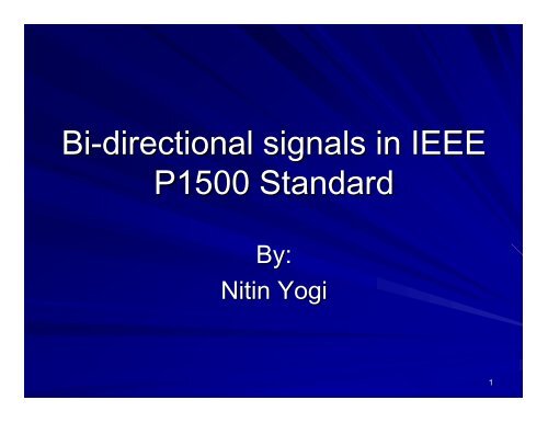
Bi-directional Bi directional signals in <strong>IEEE</strong><br />
<strong>P1500</strong> Standard<br />
By:<br />
Nitin Yogi<br />
1
Why is testing important ?<br />
Need to ascertain that manufactured chips<br />
work.<br />
Testing saves cost of replacement and<br />
compensation for faulty chips.<br />
Testing enables detection of design errors<br />
2
System on Chip (SoC ( SoC)<br />
System on Chip (SoC ( SoC) ) is a chip which holds all<br />
the necessary hardware to make a complete<br />
electronic system.<br />
SoCs comprise on-chip on chip memory, processors,<br />
peripheral devices, I/O logic control and other<br />
components each referred to as cores.<br />
3
SoC Example<br />
Advantech’s EVA-X1610C: EVA X1610C: 16-bit, 16 bit, 75 MHz<br />
RISC microprocessor with Ethernet and RS-232 RS 232 connectivity<br />
4
SoC testing<br />
SoC design has primarily evolved around<br />
core design and core reuse.<br />
Usage of pre-designed pre designed re-usable re usable<br />
embedded cores is fast becoming a popular<br />
practice in industry for SoC design.<br />
SoC testing is also based on core level<br />
testing and core test reuse.<br />
Design for Testability (DFT) methodology<br />
suits well to core-level core level testing of SoCs<br />
5
<strong>IEEE</strong> <strong>P1500</strong><br />
Proposed DFT based SoC test standard<br />
that facilitates embedded core testing and<br />
core test reuse<br />
Standardizes test information transfer<br />
model and on-chip on chip test access hardware.<br />
– The Core Test Language (CTL) is the<br />
information transfer model of the <strong>P1500</strong>.<br />
– The Scalable Test Access Architecture<br />
comprises the hardware guidelines.<br />
6
Scalable Core Test Architecture<br />
The Scalable Core Test Architecture comprises:<br />
- Source and Sink for test stimuli and responses.<br />
- Test Access Mechanism (TAM)<br />
- Wrapper<br />
The source and sink for test stimuli are provided by the<br />
testing equipment.<br />
TAMs are mechanisms used to transfer test vectors<br />
and responses to and from the core, respectively.<br />
Wrappers exists around each core to connect TAMs to<br />
the cores.<br />
7
Scalable Core Test Architecture<br />
(System-level (System level overview)<br />
8
Scalable Core Test Architecture<br />
(SoC SoC test view)<br />
9
Test Access Mechanisms (TAMs ( TAMs)<br />
TAMs are characterized by:<br />
- TAM width: determines the test<br />
data transport bandwidth.<br />
- TAM length: the physical<br />
distance of the TAM.<br />
10
Wrapper<br />
Wrapper connects the TAM to the core and thus<br />
determines the <strong>no</strong>rmal or testing mode of the core.<br />
One wrapper exists for each core and totally<br />
encapsulates the core.<br />
Unwrapped Core Wrapped Core showing wrapper<br />
architecture<br />
11
Wrapper<br />
The Wrapper Serial Input and Output are<br />
serial interfaces to the wrapper.<br />
The Wrapper Bypass Register routes data<br />
flowing from WSI to WSO, to bypass the core.<br />
12
Wrapper Instruction Register (WIR)<br />
WIR loads and executes test instructions.<br />
WIR is a SHIFT/UPDATE register, similar to JTAG’s<br />
instruction register<br />
WIR configures the operation of the wrapper, according<br />
to the instruction shifted into it.<br />
WIR circuitry decodes loaded instructions and provides<br />
individual control signals to WBR, WBY or Data registers.<br />
13
Wrapper Interface Port<br />
WIP comprises of control signals applied to the WIR and determine determine<br />
the<br />
functioning of the wrapper.<br />
WRSTN : Asynchro<strong>no</strong>us<br />
Wrapper Reset<br />
WRCK : Wrapper Clock<br />
SelectWIR : Control signal to<br />
select between Wrapper<br />
Instruction Register and<br />
Wrapper Data Registers<br />
ShiftWR : Shift control Signal<br />
CaptureWR : Capture control<br />
signal<br />
UpdateWR : Update control<br />
signal<br />
14
Wrapper Boundary Register (WBR)<br />
WBR consists of boundary<br />
scan cells (BSCs ( BSCs) )<br />
connected in series.<br />
One BSC per core terminal.<br />
Two types of BSCs defined:<br />
- BSC for input terminal<br />
- BSC for output terminal<br />
<strong>IEEE</strong> <strong>P1500</strong> <strong>does</strong> <strong><strong>no</strong>t</strong><br />
<strong>support</strong> <strong>bidirectional</strong><br />
<strong>terminals</strong>, <strong>hence</strong> <strong>no</strong><br />
<strong>bidirectional</strong> BSC is<br />
defined.<br />
Boundary Scan Cell Representation<br />
Connection of Boundary Scan Cells<br />
15
Instruction<br />
WS_BYPASS<br />
WS_EXTEST<br />
WP_EXTEST<br />
WH_EXTEST<br />
WS_INTEST_RING<br />
WS_INTEST_SCAN<br />
WP_INTEST_RING<br />
WP_INTEST_SCAN<br />
WS_PRELOAD<br />
WP_PRELOAD<br />
WS_CLAMP<br />
WS_SAFESTATE<br />
<strong>P1500</strong> Instructions<br />
Mode<br />
Normal +<br />
Serial Bypass<br />
Serial Extest<br />
Parallel Extest<br />
Hybrid Extest<br />
Serial Intest<br />
Serial Intest<br />
Parallel Intest<br />
Parallel Intest<br />
Serial Preload<br />
Parallel<br />
Preload<br />
Other<br />
Other<br />
Type<br />
Mandatory<br />
Mandatory<br />
Optional<br />
Optional<br />
At least one of<br />
them is mandatory<br />
Optional<br />
Optional<br />
Optional<br />
Optional<br />
Description<br />
Wrapper allows functional mode, WSI-WSO<br />
connected through WBY<br />
External core testing using serial interface<br />
External core testing using parallel interface<br />
External core testing using hybrid interface<br />
Internal core testing using serial interface<br />
Internal core testing using serial interface with<br />
internal core scan chains included<br />
Internal core testing using parallel interface<br />
Internal core testing using serial interface with<br />
internal core scan chains included<br />
Loads data into dedicated shift path of WBR<br />
Loads data into dedicated shift path of WBR<br />
Clamps output <strong>terminals</strong> of WBR to predefined<br />
states (Requires PRELOAD)<br />
Clamps output <strong>terminals</strong> of WBR to predefined<br />
states (Does <strong><strong>no</strong>t</strong> require PRELOAD)<br />
16
BSC Operation - BYPASS<br />
17
BSC Operation - EXTEST<br />
18
BSC Operation - INTEST<br />
19
BSC Operation – PRELOAD<br />
20
BSC implementation<br />
Input Boundary Scan Cell<br />
Output Boundary Scan Cell<br />
21
Core Test Language (CTL)<br />
CTL is the information transfer model of <strong>IEEE</strong><br />
<strong>P1500</strong><br />
CTL is an extension to the <strong>IEEE</strong> 1450 Standard<br />
Test Information Language (STIL) standard and<br />
is named as P1450.6<br />
Core providers package CTL code with their<br />
cores to make it <strong>IEEE</strong> <strong>P1500</strong> testable.<br />
CTL information includes:<br />
- Design Configuration Information<br />
- Structural Information<br />
- Test Pattern Information<br />
22
CTL Design Configuration<br />
Information<br />
Describes wrappers<br />
Describes controls to configure the core for testing<br />
the core and the surrounding SoC logic.<br />
23
CTL Structural and Test Pattern<br />
Information<br />
Structural Information<br />
- Describes requirements and<br />
constraints on the<br />
implementation of SoC<br />
level interface to the core.<br />
Test Pattern Information<br />
- Describes inclusion of test<br />
data specific to the core,<br />
but independent of any<br />
particular use of the core.<br />
24
Core pin types<br />
Input Pins - dedicated inputs<br />
Output Pins - dedicated outputs<br />
Programmable Pins - programmed as<br />
either input or output. They remain as<br />
programmed until reprogrammed<br />
Bi-directional Bi directional Pins - signals can flow either<br />
in or out of the core; direction is determined<br />
by an internal control signal<br />
25
Bi-directional Bi directional pins<br />
A bi-directional bi directional pin has tri-state tri state drivers for<br />
transmitting data and a buffer for receiving<br />
data.<br />
Difficult to test in the absence of signal<br />
direction k<strong>no</strong>wledge.<br />
26
Bi-directional Bi directional pins<br />
<strong>P1500</strong> requires <strong>bidirectional</strong> signals to be<br />
split into input, output and control signals.<br />
Disadvantage is an increase in SoC routing<br />
interconnect overhead and area.<br />
27
Testing of <strong>bidirectional</strong> signals<br />
(<strong>IEEE</strong> <strong>P1500</strong>)<br />
28
Proposed Test Structure<br />
Split bi-directional<br />
bi directional<br />
signals inside the<br />
wrapper<br />
Place input, output<br />
and control boundary<br />
scan cells on the<br />
respective signal<br />
lines<br />
Bidirectional control<br />
signal from the core<br />
controls the direction.<br />
29
BYPASS in the proposed structure<br />
30
Bidirectional BSC analysis<br />
31
BSC structure analysis<br />
32
Combining input and output BSCs<br />
Input BSC Output BSC<br />
Bidirectional BSC<br />
33
Bidirectional BSC analysis<br />
Terminal BSC Terminal REG. 2 1 => => Terminal BSC Terminal REG REG2<br />
1<br />
‘0’ ‘1’ ‘0’ ‘1’<br />
‘0’ ‘1’<br />
34
BSC Control Structure<br />
35
Conventional vs Modified Bidirectional<br />
BSC – Transistor Count<br />
Reduction of<br />
more than twice<br />
in the number<br />
of transistors<br />
36
Parameters<br />
Bypass Delay<br />
Ter.1 => Ter.2<br />
Conventional vs Modified<br />
Bidirectional BSC - Delays<br />
Drive Delay<br />
BSC reg. => Ter.<br />
Capture Delay<br />
Ter. => BSC reg.<br />
Conventional<br />
550 ps<br />
860 ps<br />
1000 ps<br />
Modified<br />
730 ps<br />
930 ps<br />
1700 ps<br />
37
Implementation of <strong>P1500</strong><br />
instructions<br />
Three <strong>IEEE</strong> <strong>P1500</strong> instructions are<br />
mandatory:<br />
WS_BYPASS / WS_PRELOAD<br />
WS_INTEST_RING / WS_INTEST_SCAN<br />
WS_EXTEST<br />
38
WS_BYPASS / WS_PRELOAD<br />
BYPASS instruction<br />
PRELOAD instruction<br />
The testing structure is disabled, although test<br />
vectors can be loaded into the cell registers.<br />
39
Implementation of WS_BYPASS /<br />
WS_PRELOAD instruction<br />
Conventional BSC<br />
40
Implementation of WS_BYPASS /<br />
WS_PRELOAD instruction<br />
Modified BSC<br />
41
WS_INTEST_RING /<br />
WS_INTEST_SCAN<br />
Testing structure is<br />
enabled and is assumed to<br />
be preloaded with test<br />
vectors.<br />
This is an inward facing<br />
test directed towards the<br />
core to test it.<br />
We need to consider two<br />
cases, <strong>bidirectional</strong> BSC<br />
configured as:<br />
- Input BSC<br />
- Output BSC<br />
42
Implementation of WS_INTEST_RING /<br />
WS_INTEST_SCAN instruction<br />
Bidirectional BSC configured as an Input BSC<br />
Conventional BSC<br />
43
Implementation of WS_INTEST_RING /<br />
WS_INTEST_SCAN instruction<br />
Bidirectional BSC configured as an Input BSC<br />
Modified BSC<br />
44
Implementation of WS_INTEST_RING /<br />
WS_INTEST_SCAN instruction<br />
Bidirectional BSC configured as an Output BSC<br />
Conventional BSC<br />
45
Implementation of WS_INTEST_RING /<br />
WS_INTEST_SCAN instruction<br />
Bidirectional BSC configured as an Output BSC<br />
Modified BSC<br />
46
WS_EXTEST<br />
The testing structure is enabled and assumed to have been<br />
preloaded with test vectors.<br />
This is an outward facing test directed towards the interconnects.<br />
interconnects.<br />
We need to consider two cases, <strong>bidirectional</strong> BSC configured as:<br />
- Input BSC<br />
- Output BSC<br />
47
Implementation of WS_EXTEST<br />
instruction<br />
Bidirectional BSC configured as an Input BSC<br />
Conventional BSC<br />
48
Implementation of WS_EXTEST<br />
instruction<br />
Bidirectional BSC configured as an Input BSC<br />
Modified BSC<br />
49
Implementation of WS_EXTEST<br />
instruction<br />
Bidirectional BSC configured as an Output BSC<br />
Conventional BSC<br />
50
Implementation of WS_EXTEST<br />
instruction<br />
Bidirectional BSC configured as an Output BSC<br />
Modified BSC<br />
51
Transmission Gates<br />
Digital switch constructed using CMOS tech<strong>no</strong>logy, which<br />
connects two <strong>terminals</strong> when activated and disconnects<br />
them when deactivated.<br />
Consists of an NMOS and a PMOS transistor<br />
– An NMOS transistor turns ON when logic ‘1’ is applied to its gate gate<br />
terminal.<br />
– A PMOS transistor turns ON when logic’0’ is applied to its gate<br />
terminal.<br />
52
Transmission Gate Issues<br />
Requires both NMOS and PMOS transistors<br />
Requires use of complementary control signal.<br />
Leakage current due to <strong>no</strong>n-infinite <strong>no</strong>n infinite OFF<br />
impedance.<br />
– Can be reduced by proper scaling of MOS transistors<br />
and proper design of the circuits connected to<br />
transmission gate.<br />
Major issues:<br />
- serial loading due to finite ON impedance<br />
- absence of inherent driving capability.<br />
53
Solutions to Transmission Gate<br />
low-drive low drive issue.<br />
1. Connect additional circuit to the signal line in parallel with<br />
the transmission gate structure:<br />
- Bus-hold Bus hold circuit<br />
- Bidirectional repeater<br />
2. Replace the transmission gate structure so that it provides<br />
sufficient drive strength along with the <strong>bidirectional</strong> switch<br />
functionality.<br />
Receiver<br />
CORE<br />
Transmitter<br />
Control Signal<br />
Bidirectional<br />
BSC<br />
WRAPPER<br />
Bus-Hold /<br />
Bidirectional<br />
Repeater Circuit<br />
Bidirectional signal line<br />
54
Bus-Hold Bus Hold Circuit<br />
Provides a defined logic state to floating<br />
buses.<br />
Acts as a bus-hold bus hold circuit and a logic restorer<br />
and driver circuit, due to the driving inverters.<br />
The drive delay was found to be 300ps.<br />
55
Bidirectional repeater circuit<br />
Combination of positive and<br />
negative feedback keeps the<br />
output <strong>no</strong>de in high<br />
impedance state.<br />
On signal transition, driver<br />
circuit is enabled by positive<br />
feedback.<br />
The delayed negative<br />
feedback disables the driver<br />
circuit later.<br />
The drive delay was found to<br />
be 250ps.<br />
56
Buffered Memory Cell<br />
Consists of two back-to back to-<br />
back inverters with a<br />
transmission gate at the<br />
output of each inverter.<br />
The transmission gate<br />
reduces the loading of<br />
the output inverters.<br />
Provides required drive<br />
for the signal line and<br />
acts as a <strong>bidirectional</strong><br />
switch.<br />
57
Comparison of signal boosting<br />
circuits (driving logic ‘0’)<br />
58
Comparison of signal boosting<br />
circuits (driving logic ‘1’)<br />
59
Comparison of signal boosting<br />
Parameters<br />
Transition delay of the<br />
signal line under<br />
consideration<br />
Drive Delay<br />
Steady State<br />
Characteristics<br />
Transition State<br />
Characteristics<br />
Bus-contention<br />
resistance<br />
Drive Duration<br />
Drive Strength<br />
Driver<br />
NO<br />
Bus-Hold circuit<br />
May affect to some extent,<br />
as the bus-hold circuit<br />
can load the signal<br />
line.<br />
Transition delay of two<br />
inverters and one<br />
transmission gate.<br />
Equal to 300ps*<br />
Loads the signal line<br />
Continuous except the drive<br />
delay<br />
Drives 600uA at V out = 3.5V,<br />
and sinks 600uA at<br />
V out = 1.5V<br />
circuits<br />
High-impedance state<br />
Driver<br />
NO<br />
Bidirectional Repeater<br />
Does <strong><strong>no</strong>t</strong> affect, as the<br />
<strong>bidirectional</strong> repeater<br />
<strong>does</strong> <strong><strong>no</strong>t</strong> load the signal<br />
line.<br />
Transition delay of inverter in<br />
positive feedback.<br />
Equal to 250ps*<br />
For a duration equal to the<br />
gate delay in the<br />
negative feedback from<br />
the transition point<br />
Drives 600uA at V out = 3.5V,<br />
and sinks 560uA at V out =<br />
1.5V<br />
Transition delay of two<br />
inverters and one<br />
transmission gate<br />
Transition delay of two<br />
inverters and one<br />
transmission gate.<br />
Equal to 440ps*<br />
Driver<br />
Driver<br />
YES<br />
Buffered Memory Cell<br />
Continuous<br />
Drives 150uA at V = 3.5V,<br />
out<br />
and sinks 250uA at<br />
V = 1.5V<br />
out<br />
60
Testing <strong>bidirectional</strong> signals<br />
In the absence of <strong>bidirectional</strong> control signal, testing of<br />
<strong>bidirectional</strong> signals can be performed in two ways:<br />
ways<br />
Synchronizing the directions of the <strong>bidirectional</strong> signal<br />
lines in the core and the wrapper, through proper test<br />
planning and design.<br />
- Disadvantage: Synchronization puts additional<br />
responsibility and overhead on the test planner and<br />
programmer.<br />
Place the driver in the wrapper which faces the core to be<br />
a weak driver.<br />
- Disadvantage: Weak driver issues like power<br />
consumption.<br />
61
Weak Drivers<br />
Required in the absence of <strong>bidirectional</strong> control<br />
signal and difficulty of synchronization between<br />
core and wrapper.<br />
Can be constructed using Transmission Gates<br />
Operation is similar to the Buffered Memory Cell.<br />
62
Strong vs weak Drivers<br />
Characteristics of interaction of a strong driver driving logic ‘0’ and a weak driver<br />
driving logic ‘1’<br />
63
Strong vs weak Drivers<br />
Characteristics of interaction of a strong driver driving logic ‘1’ and a weak driver<br />
driving logic ‘0’<br />
64
Summary<br />
Examined problems related to testing of<br />
<strong>bidirectional</strong> lines for <strong>IEEE</strong> <strong>P1500</strong> standard.<br />
Designed and modified <strong>bidirectional</strong> BSC<br />
structure.<br />
Compared modified <strong>bidirectional</strong> BSC<br />
structure with the conventional structure.<br />
– Modified <strong>bidirectional</strong> boundary scan structure<br />
utilizes 35 to 40% less transistors depending on<br />
the bus width.<br />
– Modified structure has nearly similar propagation<br />
delays.<br />
65
Summary<br />
Analyzed problems associated with transmission<br />
gates which were used in the modified structure<br />
and suggested solutions to it.<br />
Studied different signal boosting circuits to<br />
alleviate problems of driving capability and<br />
loading associated with transmission gates.<br />
The main signal boosting circuits studied were<br />
bus hold circuit, <strong>bidirectional</strong> repeater circuit and<br />
buffered memory cell structure.<br />
66
Summary<br />
Implementation details of conventional and the modified<br />
<strong>bidirectional</strong> boundary scan structures and also their<br />
functioning for different test instructions as prescribed by<br />
<strong>IEEE</strong> <strong>P1500</strong> standard were discussed.<br />
The proposed modified <strong>bidirectional</strong> boundary scan<br />
structure can be implemented successfully in designs<br />
with efficient utilization of chip area.<br />
Structure suffers from some longer propagation delay<br />
issues which can be alleviated by use of a faster<br />
tech<strong>no</strong>logy, efficient logic synthesis, manipulation of<br />
control signals for the control structure.<br />
Heavy reliance on transmission gates is a shortcoming<br />
of the modified structure since <strong><strong>no</strong>t</strong> all tech<strong>no</strong>logies<br />
<strong>support</strong> it.<br />
67
THANK YOU !<br />
Questions ?<br />
Thank you for attending this seminar<br />
68