Toy Motor Driver Series MX214B
Toy Motor Driver Series MX214B
Toy Motor Driver Series MX214B

You also want an ePaper? Increase the reach of your titles
YUMPU automatically turns print PDFs into web optimized ePapers that Google loves.
<strong>MX214B</strong><br />
<strong>Toy</strong> <strong>Motor</strong> <strong>Driver</strong> <strong>Series</strong><br />
Features<br />
● Low static operating current<br />
● Wide supply voltage range:2.5V‐10V<br />
● Continuous output current capability of 800mA<br />
/channel)<br />
● Built‐in thermal shutdown function<br />
● Lower saturation voltage<br />
● Has overtemperature protection function<br />
● Three functions ‐Forward/Reverse/ High Impedance<br />
● Compatible with TTL/CMOS interface,connects<br />
directly to CPU<br />
● Built‐in clamp diodes suitable for inductive load<br />
● Control and drive circuit integrated into a single IC<br />
● Suitable for 3 to 6 batteries operated application<br />
● Internal ESD protection (4000V HBM)<br />
● Operating temperature range:‐20℃—+80℃<br />
Typical Application<br />
● <strong>Toy</strong> car motor drive<br />
Ordering Guide<br />
<strong>Toy</strong> <strong>Motor</strong> <strong>Driver</strong> <strong>Series</strong> <strong>MX214B</strong><br />
Description<br />
The <strong>MX214B</strong> is a dual‐channel push‐pull power<br />
amplification application‐specific IC device designed<br />
to control and drive toy motor, integrates discrete<br />
devices into a monolithic IC, decreases cost of<br />
periphery, and increases reliability of the whole unit.<br />
All inputs of the chip are TTL/CMOS‐compatible, and<br />
have a good interference immunity. The circuit has a<br />
greater current‐driving capability, continuous<br />
current/channel is 750 mA to 800 mA, peak current<br />
reaches 1.5A to 2.0A, the circuit has overtemperature<br />
protection function, and on‐chip clamping diode<br />
releases reverse impulse current of inductive load.<br />
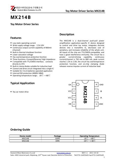
OA<br />
VCC<br />
VCC<br />
OB<br />
<strong>MX214B</strong><br />
Device model Package Operating Temperature<br />
<strong>MX214B</strong> SOP8 ‐20℃—+80℃<br />
<strong>MX214B</strong> DIP8 ‐20℃—+ 80℃<br />
Sinotech Mixic Electronics Co.,Ltd www.mixic.com.cn REV 1.1 2011‐10‐18<br />
Sales: A402 industrial park, Majialong, 125 th Yiyuan road ,Nanshan district of Shenzhen Tel:0755‐26895685 Fax:0755‐26895685<br />
1<br />
1<br />
2<br />
3<br />
4<br />
8<br />
7<br />
6<br />
5<br />
GND<br />
IB<br />
IA<br />
GND
Sinotech Mixic Electronics Co.,LTD <strong>MX214B</strong><br />
Pin Function Descriptions<br />
Pin Number Mnemonic I/O Pin Function Description<br />
1 OA O A channel output<br />
2 VCC ‐ Supply voltage output<br />
3 VCC ‐ Supply voltage output<br />
4 OB O B channel output<br />
5 GND ‐ Ground<br />
6 IA I A channel input<br />
7 IB I B channel input<br />
8 GND ‐ Ground<br />
Schematics of Inputs and Outputs<br />
FUNCTIONAL BLOCK DIAGRAM<br />
Sinotech Mixic Electronics Co.,Ltd www.mixic.com.cn REV 1.1 2011‐10‐18<br />
Sales: A402 industrial park, Majialong, 125 th Yiyuan road ,Nanshan district of Shenzhen Tel:0755‐26895685 Fax:0755‐26895685<br />
2
Sinotech Mixic Electronics Co.,LTD <strong>MX214B</strong><br />
Logic Truth Table<br />
IA IB OA OB<br />
H L H L<br />
L H L H<br />
L L Z(High Impedance) Z (High Impedance)<br />
H H Z(High Impedance) Z (High Impedance)<br />
Input IA<br />
Input IB<br />
Output OA<br />
Output OB<br />
Forward<br />
(Reverse)<br />
Reverse<br />
(Forward)<br />
Sinotech Mixic Electronics Co.,Ltd www.mixic.com.cn REV 1.1 2011‐10‐18<br />
Sales: A402 industrial park, Majialong, 125 th Yiyuan road ,Nanshan district of Shenzhen Tel:0755‐26895685 Fax:0755‐26895685<br />
3<br />
Z<br />
Z
Sinotech Mixic Electronics Co.,LTD <strong>MX214B</strong><br />
Absolute Maximum Ratings<br />
(TA=25℃,unless<br />
otherwise specified)<br />
Parameter Symbol<br />
Min.<br />
Value<br />
Typ. Max.<br />
Unit<br />
Supply voltage<br />
VCC 2.5 6.0 10 V<br />
Peak output current IMax<br />
‐ 1500 2000 mA<br />
Input high level VHIN<br />
2.5 5.0 10 V<br />
Input low level VLIN<br />
‐ 0.5 0.7 V<br />
Thermal resistance θJA<br />
SOP8 ‐ ‐ 160 ℃ /W<br />
(1)<br />
DIP8 ‐ ‐ 100 ℃ /W<br />
Maximum operating junction<br />
temperature<br />
T J<br />
‐ ‐ 150 ℃<br />
Soldering temperature<br />
‐ ‐ 260 ℃,10S<br />
Storage temperature Range<br />
Tstg ‐65 ‐ 150 ℃<br />
NOTE:(1)Maximum power dissipation can be obtained from the following formula<br />
P = ( T − T ) / θ<br />
D<br />
J<br />
A<br />
JA<br />
Where TJ is junction temperature with the circuit working, and TA is the ambient temperature with the circuit<br />
working. Calculation of thermal impedance of package is as per ESD 51‐7.<br />
Recommended Operating Conditions<br />
(TA=25℃,unless otherwise specified)<br />
Range<br />
Parameter Symbol Condition Unit<br />
Min. Typ. Max.<br />
Supply voltage<br />
VCC 3.0 ‐ 9.0 V<br />
Continuous output current IOUT<br />
400 600 800 mA<br />
(1)<br />
Operating temperature range T A<br />
‐20 ‐ 80 ℃<br />
(2)<br />
SOP8 ‐ ‐ 625 mW<br />
Power dissipation PD<br />
DIP8 ‐ ‐ 1250 mW<br />
NOTES: (1) TA is the ambient temperature at the time that circuit operates;<br />
(2) The power dissipation Pd is given by:<br />
PD=I OUT×V O(sat) +(I VCC‐I OUT) ×VCC+V IA×I IA+V IB×IIB where I OUT is the output current through the circuit or driving motor; VO(sat)<br />
is output saturation voltage<br />
of circuit; IVCC is the current flowing into power supply pin VCC; VCC is the voltage at power supply pin VCC;<br />
V IA and V IB are the input voltage at power supply pins IA and IB, respectively; I IA and IIB<br />
are the input current<br />
at power supply pins IA and IB, respectively.<br />
In above expression, PD is mostly determined by I OUT×VO(sat), where for the relation between output<br />
saturation voltage VO(sat) and output current IOUT of circuit the typical parameter curves in Fig. 6 can be<br />
referred to. If the internal resistance of a motor is RM,<br />
then a straight line VO(sat)= VCC ‐ I OUT×RM is drawn in<br />
Fig. 6. From the point of intersection of the straight line with the curve in Fig. 6, VO(sat) and IOUT can be<br />
obtained. In combination with practical application and power dissipation, internal resistance of a motor (RM)<br />
is determined, and so a proper motor can be selected.<br />
To make circuit operate safely and normally, make sure that circuit power dissipation is in the range<br />
allowed.<br />
Sinotech Mixic Electronics Co.,Ltd www.mixic.com.cn REV 1.1 2011‐10‐18<br />
Sales: A402 industrial park, Majialong, 125 th Yiyuan road ,Nanshan district of Shenzhen Tel:0755‐26895685 Fax:0755‐26895685<br />
4
Sinotech Mixic Electronics Co.,LTD <strong>MX214B</strong><br />
Electrical Characteristics<br />
(Unless otherwise specified, VCC=5V, TA=25℃)<br />
Parameter Fig. for test Condition Min. Typ. Max. Unit<br />
I DD Quiescent current 1 ‐ 0.1 2.0 uA<br />
IIN Input current 2 V IA=H,V OA=H<br />
‐ 500 700 uA<br />
I =500mA (2)<br />
VO ( sat ) Output saturation<br />
(1)<br />
voltage<br />
3<br />
OUT<br />
IOUT=200mA<br />
‐<br />
‐<br />
1.00<br />
0.75<br />
1.15<br />
0.85<br />
V<br />
V<br />
IOUT Continuous output<br />
current<br />
3<br />
SOP8 750 800 850 mA<br />
DIP8 900 1000 1100 mA<br />
IMax Peak output current 3 ‐ 1500 2000 mA<br />
Tsd Over‐temperature<br />
shutdown<br />
Tsdh Over‐temperature<br />
shutdown hysteresis<br />
VCC=6V 165<br />
VCC=6V 30 ℃<br />
NOTES:(1) The output saturation voltage is the sum of output high‐ and low‐side saturation voltages,i.e. the sum<br />
of the measured values in voltmeters V1 and V2 in Fig.3.<br />
(2) By adjusting adjustable resistor R in Fig. 3, the stated current can be obtained from reading of<br />
ammeter.<br />
Test Circuit Diagrams<br />
Fig. 1 (Quiescent current I DD) Fig. 2 (Input current IIN)<br />
Fig. 3 (Output saturation voltage VO(sat)=V1+V2)<br />
Sinotech Mixic Electronics Co.,Ltd www.mixic.com.cn REV 1.1 2011‐10‐18<br />
Sales: A402 industrial park, Majialong, 125 th Yiyuan road ,Nanshan district of Shenzhen Tel:0755‐26895685 Fax:0755‐26895685<br />
5<br />
℃
Sinotech Mixic Electronics Co.,LTD <strong>MX214B</strong><br />
Typical Electrical Characteristic Curves<br />
High‐side saturation voltage VSAT(V1)(V)<br />
Sum of high‐ and low‐side saturation voltage VSAT(V1+V2)<br />
High‐side saturation voltage VSAT(V1) VS output current IO<br />
VCC=3V<br />
VCC=5V VCC=9V<br />
Output current IO(mA)<br />
Fig. 4 High‐side saturation voltage VS output<br />
current<br />
Sum of high‐ and low‐side saturation voltage VSAT(V1+V2) VS<br />
output current IO<br />
VCC=3V<br />
VCC=5V<br />
Output current IO(mA)<br />
Fig. 6 Sum of high‐ and low‐side saturation<br />
voltage VS output current<br />
VCC=9V<br />
Typical Application Circuit Diagrams<br />
Low‐side saturation voltage VSAT(V2) VS output current IO<br />
Sinotech Mixic Electronics Co.,Ltd www.mixic.com.cn REV 1.1 2011‐10‐18<br />
Sales: A402 industrial park, Majialong, 125 th Yiyuan road ,Nanshan district of Shenzhen Tel:0755‐26895685 Fax:0755‐26895685<br />
6<br />
Low‐side saturation voltage VSAT(V2)(V)<br />
VCC=3V<br />
VCC=5V<br />
Output current IO(mA)<br />
VCC=9V<br />
Fig. 5 Low‐side saturation voltage VS output current<br />
Output current IO(mA)<br />
Output current IO(mA) VS load resistance RO(Ω)<br />
VCC=3V<br />
VCC=5V<br />
VCC=9V<br />
Load resistance RO(Ω)<br />
Fig. 7 Output current VS load resistance
Sinotech Mixic Electronics Co.,LTD <strong>MX214B</strong><br />
Packages<br />
SOP8:<br />
SYMBOL<br />
θ<br />
MILLIMETER<br />
MIN NOM MAX<br />
A ‐‐ ‐‐ 1.77<br />
A1 0.08 0.18 0.28<br />
A2 1.20 1.40 1.60<br />
A3 0.55 0.65 0.75<br />
b 0.39 ‐‐ 0.48<br />
b1 0.38 0.41 0.43<br />
c 0.21 ‐‐ 0.26<br />
c1 0.19 0.20 0.21<br />
D 4.70 4.90 5.10<br />
E 5.80 6.00 6.20<br />
E1 3.70 3.90 4.10<br />
e 1.27BSC<br />
L 0.50 0.65 0.80<br />
L1 1.05BSC<br />
θ 0 ‐‐ 8°<br />
Sinotech Mixic Electronics Co.,Ltd www.mixic.com.cn REV 1.1 2011‐10‐18<br />
Sales: A402 industrial park, Majialong, 125 th Yiyuan road ,Nanshan district of Shenzhen Tel:0755‐26895685 Fax:0755‐26895685<br />
7
Sinotech Mixic Electronics Co.,LTD <strong>MX214B</strong><br />
DIP8:<br />
b B1<br />
B B<br />
e<br />
SYMBOL<br />
D<br />
A3<br />
A2<br />
E1<br />
A<br />
A1 L<br />
c<br />
BASE<br />
METAL<br />
eA<br />
eB<br />
b1 b<br />
c1 c<br />
eC<br />
WITH PLATING<br />
SECTION B-B<br />
MILLIMETER<br />
MIN NOM MAX<br />
A 3.60 3.80 4.00<br />
A1 0.51 _ _<br />
A2 3.10 3.30 3.50<br />
A3 1.50 1.60 1.70<br />
b 0.44 _ 0.53<br />
b1 0.43 0.46 0.48<br />
B1 1.52BSC<br />
c 0.25 _ 0.31<br />
c1 0.24 0.25 0.26<br />
D 9.05 9.25 9.45<br />
E1 6.15 6.35 6.55<br />
e 2.54BSC<br />
eA 7.62BSC<br />
eB 7.62 _ 9.50<br />
eC 0 _ 0.94<br />
L 3.00 _ _<br />
Sinotech Mixic Electronics Co.,Ltd www.mixic.com.cn REV 1.1 2011‐10‐18<br />
Sales: A402 industrial park, Majialong, 125 th Yiyuan road ,Nanshan district of Shenzhen Tel:0755‐26895685 Fax:0755‐26895685<br />
8