

program and abstracts
program and abstracts
program and abstracts

Create successful ePaper yourself
Turn your PDF publications into a flip-book with our unique Google optimized e-Paper software.
SUPPORTERS<br />
Verein zur Durchführung der<br />
International Winterschool on Electronic Properties of Novel Materials<br />
Verein zur Förderung der Internationalen Winterschulen in Kirchberg Austria<br />
PATRONAGE<br />
Ewald Haller<br />
Bürgermeister von Kirchberg<br />
SPONSORS<br />
Applied Nanofluorescence,<br />
3701 Kirby Drive, Suite 994, Houston, TX 77098, USA<br />
HORIBA Jobin Yvon GmbH,<br />
Neuhofstrasse 9, 64625 Bensheim, Germany<br />
Wiley-VCH Verlag GmbH & Co. KGaA,<br />
Boschstraße 12, 69469 Weinheim, Germany<br />
SINEUROP Nanotech GmbH,<br />
Kernerstr. 34, 70182 Stuttgart, Germany<br />
L.O.T.-Oriel GmbH,<br />
Im Tiefen See 58, 64293 Darmstadt, Germany<br />
NACALAI TESQUE, INC.,<br />
Nijo Karasuma, Nakagyo-ku Kyoto, 604-0855 Japan<br />
Financial assistance from the sponsors <strong>and</strong> supporters is greatly acknowledged.<br />
1
Dear Friend:<br />
Welcome to the 23 rd International Winterschool on:<br />
Electronic Properties of Novel Materials: “Molecular nanostructures”<br />
This Winterschool is a sequel of twenty-two previous meetings held in Kirchberg in<br />
the last decades on problems related to the electronic structure of novel materials.<br />
The idea of the meeting is to bring together experienced scientists from universities<br />
<strong>and</strong> industry with advanced students working in the selected field <strong>and</strong> thus create<br />
a fruitful <strong>and</strong> prosperous community for the exchange of scientific information <strong>and</strong><br />
personal experience. It is a tradition of the Winterschools in Kirchberg that this<br />
exchange is not restricted to the lectures <strong>and</strong> poster sessions but occurs throughout<br />
the whole week.<br />
The Winterschool is dedicated to molecular nanostructures as a new class of materials.<br />
Like the previous Winterschools it runs on an informal level.<br />
If you have any questions concerning the organization <strong>and</strong> the <strong>program</strong>, come <strong>and</strong><br />
see one of us or one of the colleagues involved in the preparation of the meeting.<br />
These persons are:<br />
Janina Maultzsch <strong>program</strong><br />
Matthias Müller accomodation, sponsoring<br />
Nils Rosenkranz registration, finance<br />
Marcel Mohr video transfer <strong>and</strong> recording, internet<br />
Hagen Telg general assistance<br />
Harald Scheel receipts, technical assistance<br />
Dirk Heinrich technical assistance<br />
Norman Tschirner computer, internet, e-payment<br />
Also the managers of the hotel, Frau Mayer <strong>and</strong> her son Herr Mayer, <strong>and</strong> their staff<br />
promised to help us wherever they can. We want to acknowledge their help <strong>and</strong><br />
also that of Sabine Morgner in the organization of the IWEPNM 2009.<br />
We wish you an interesting, successful, <strong>and</strong> pleasant week in Kirchberg. We are<br />
very much looking forward to your contributions at the event.<br />
Sincerely yours, Christian, Peter, Hans, <strong>and</strong> Siegmar<br />
3
Chairmen<br />
C. Thomsen (Berlin)<br />
P. Dinse (Darmstadt)<br />
H. Kuzmany (Vienna)<br />
S. Roth (Stuttgart)<br />
Program Committee<br />
A. Bachtold (ES) F. Mauri (FR)<br />
P. Dinse (DE) M. Mehring (DE)<br />
M. Dresselhaus (US) K. S. Novoselov (UK)<br />
S. Fan (CN) E. Obraztsova (RU)<br />
J. E. Fischer (US) Th. Pichler (AT)<br />
L. Forro (CH) J. Robertson (UK)<br />
T. F. Heinz (US) A. Rubio (ES)<br />
A. Hirsch (DE) S. Roth (DE)<br />
S. Iijima (JP) P. Rudolf (NL)<br />
H. Kataura (JP) C. Schönenberger (CH)<br />
P. Kouwenhoven (NL) N. Shinohara (JP)<br />
H. W. Kroto (UK) Z. K. Tang (CN)<br />
H. Kuzmany (AT) C. Thomsen (DE)<br />
Y. H. Lee (KR) A. Zettl (US)<br />
A. Loiseau (FR) D. Zhu (CN)<br />
Scope<br />
This winterschool will provide a platform for reviewing <strong>and</strong> discussing new developments<br />
in the field of electronic properties of molecular nanostructures <strong>and</strong> their<br />
applications. Subjects included are: • Materials science of graphene <strong>and</strong> nanoribbons<br />
• Carbon nanotube optics <strong>and</strong> electronics • Carbon nanotube growth <strong>and</strong><br />
selection • Single-molecule experiments • Applications of molecular nanostructures<br />
• Theory of molecular nanostructures • Biomolecule physics <strong>and</strong> applications •<br />
Nanostructure spintronics<br />
4
INFORMATION FOR PARTICIPANTS<br />
Time <strong>and</strong> location<br />
The IWEPNM 2009 starts on Saturday, 7 March, evening, at the hotel Sonnalp in<br />
Kirchberg/Tirol, Austria <strong>and</strong> extends to Saturday, 14 March, breakfast. There will<br />
be a reception party on 7 March, after dinner, <strong>and</strong> a farewell party including dinner<br />
on Friday, 13 March.<br />
Transport<br />
The hotel Sonnalp can be reached by private car from downtown Kirchberg by<br />
driving about one kilometer towards Aschau. Participants arriving at the railway<br />
station in Kirchberg or Kitzbühel should hire a taxi to get to the hotel.<br />
Addresses<br />
The address of the Winterschool is:<br />
IWEPNM 2009, Hotel Sonnalp, A–6365 Kirchberg/Tirol, Austria<br />
Tel: ++43 5357 27410, Fax: ++43 5357 2741 200<br />
e-mail: info@hotelsonnalp.info, Web: www.tiscover.at/sonnalp.parkhotel<br />
All questions concerning the IWEPNM 2009 should be directed to:<br />
Prof. Christian Thomsen,<br />
Institut für Festkörperphysik,<br />
Technische Universität Berlin<br />
Hardenbergstr. 36, 10623 Berlin, Germany<br />
Tel: +49-(0)30-31423187, Fax: +49-(0)30-31427705<br />
email: iwepnm-info@physik.tu-berlin.de<br />
Web: http://www.iwepnm.org<br />
Participation<br />
Participation at the IWEPNM 2009 is possible for students <strong>and</strong> scientists working<br />
in the field covered by the scope of the meeting. Because of the limited space the<br />
participation requires prearranged acceptance by the organizers.<br />
Contributions<br />
All oral contributions will be presented in the big seminar room of the Hotel Sonnalp.<br />
Participants are invited to contribute comments to research <strong>and</strong> tutorial lectures<br />
where 10 minutes for discussion are reserved after each lecture. Video projection<br />
will be available for presentations. Presentation of video films needs prearranged<br />
confirmation. Invited speakers please test the video projection with the technical<br />
staff at the latest a few minutes before your session begins. Posters will be presented<br />
in the hall of the seminar room.<br />
5
During the conference<br />
If you want to buy a ticket for the ski lifts in the Kirchberg/Kitzbühel area, please<br />
ask at the hotel reception on Saturday evening. Internet connection through WLAN<br />
is available for all participants, even if they are not accommodated at the Hotel<br />
Sonnalp. Please check at the front desk.<br />
Proceedings<br />
The contributions to the IWEPNM 2009 will be published in physica status solidi.<br />
The expected date for the appearance of the proceedings is September 2009.<br />
Contributions can only be published if they arrive before the 30 April.<br />
Online submission will be used, which you can find under the following address:<br />
http://conferences.wiley-vch.de/v3. The manuscripts will be reviewed within the<br />
following weeks. Acceptance of a contribution for presentation at the Winterschool<br />
does not automatically include acceptance for publication in the proceedings.<br />
Manuscript preparation<br />
Make sure to refer to the current version of the instructions for authors:<br />
http://www3.interscience.wiley.com/cgi-bin/jabout/40000761/instructions.html<br />
In particular, the following requirements should be met:<br />
• Your manuscript should be written using our Word<br />
http://www.wiley-vch.de/vch/journals/2231/public/pss abc 2008 word.zip<br />
or LaTeX<br />
http://www.wiley-vch.de/vch/journals/2231/public/pss abc 2008 latex.zip<br />
template.<br />
• Relevant PACS numbers (a maximum of six codes) must be given, see the full<br />
<strong>and</strong> most recent classification system (PACS 2008) at http://www.aip.org/pacs.<br />
Always use the complete form, such as 32.50.+i, 71.70.Ej. The page limit for<br />
invited oral talks is 6 for poster contributions 4 pages. Submission deadline<br />
is April 30, 2009.<br />
Manuscript submission<br />
For online submission please go to http://conferences.wiley-vch.de/v3. Your login<br />
details will be emailed to you by the conference organizers in due time. Select<br />
PHYSICA STATUS SOLIDI as the journal <strong>and</strong> choose IWEPNM 2009 from the<br />
list of projects. Once you there, click on “Create manuscript” on the left side of the<br />
screen <strong>and</strong> follow the instructions.<br />
File names<br />
Please use only Western letters for the file name, <strong>and</strong> only lower-case letters for the<br />
format extension. Please use clear, self-explaining file names.<br />
Example: smith version2.doc. Please note that after submitting a manuscript, you<br />
can no longer modify it.<br />
6
IWEPNM 2009<br />
CHAIRPERSONS FOR THE ORAL SESSIONS<br />
The following participants are asked to support the <strong>program</strong> of the Winterschool<br />
by serving as chairperson:<br />
Sunday, 8.03. morning Mehring<br />
morning, after coffee break Loiseau<br />
evening Pichler<br />
Monday, 9.03. morning Kuzmany<br />
morning, after coffee break Saito, R.<br />
evening Kaiser, A.<br />
Tuesday, 10.03. morning Novoselov<br />
morning, after coffee break Maruyama<br />
evening Obraztsova<br />
Wednesday, 11.03. morning Mauri<br />
morning, after coffee break Kürti<br />
evening Hartschuh<br />
Thursday, 12.03. morning Robertson<br />
morning, after coffee break Roth<br />
evening Forro<br />
Friday, 13.03. morning Bockrath<br />
morning, after coffee break Dinse<br />
evening Kamaras<br />
Chairpersons are asked to start the sessions in time <strong>and</strong> to terminate the lectures<br />
according to schedule. The discussions may be extended up to 5 minutes beyond<br />
the schedule.<br />
Chairpersons please remember: You have to ask for questions from the sideroom<br />
(bar)!<br />
Chairpersons please remember: For questions from the main room please ask<br />
the speaker to repeat the question. The chairperson’s microphone should<br />
only be passed on to questions from the first row.<br />
If there are any objections to the suggested list of chairpersons, please let us know<br />
at the beginning of the Winterschool.<br />
We acknowledge your support.<br />
The Organizers<br />
7
Topics<br />
8:30<br />
9:00<br />
9:30<br />
10:00<br />
10:30<br />
11:00<br />
11:30<br />
Final Program<br />
Sunday 8 March Monday 9 March Tuesday 10 March Wednesday 11 March Thursday 12 March Friday 13 March<br />
Synthesis <strong>and</strong><br />
selection of carbon<br />
nanotubes<br />
High efficiency metalsemiconductor<br />
separation<br />
of SWNTs by using<br />
agarose gel<br />
KATAURA<br />
In situ electron micros-<br />
copy observations on<br />
CNTs <strong>and</strong> related<br />
structures during<br />
deformations, growth <strong>and</strong><br />
transformations<br />
JIN<br />
Graphene I <strong>and</strong><br />
quantum dots<br />
Electronic properties of Graphene: the magic of<br />
pristine <strong>and</strong> doped carbon flat carbon<br />
nanotubes<br />
NOVOSELOV<br />
SAITO, S.<br />
Preparation,<br />
characterization, <strong>and</strong><br />
application of<br />
monodisperse single- <strong>and</strong><br />
double-walled CNTs<br />
HERSAM<br />
Separating SWNTs by<br />
length, electronic property<br />
<strong>and</strong> chiral index<br />
KAPPES<br />
Low-voltage high<br />
resolution TEM of carbon<br />
nanomaterials<br />
WARNER<br />
Spin injection, transport<br />
<strong>and</strong> manipulation in<br />
graphene field effect<br />
transistors.<br />
VAN WEES<br />
Graphene <strong>and</strong> graphene<br />
superlattices: pseudospin,<br />
electron-electron <strong>and</strong><br />
electron-phonon effects<br />
LOUIE<br />
Electron-phonon coupling<br />
in graphene<br />
ATTACALITE<br />
Stability, chemical<br />
structure, <strong>and</strong> Clar's<br />
aromatic sextets of<br />
hydrogen-terminated<br />
graphene ribbons<br />
MAURI<br />
Graphene II <strong>and</strong><br />
theory of carbon<br />
nanotubes<br />
Graphene mechanics,<br />
tribology, Raman spectra<br />
under strain, <strong>and</strong> NEMS<br />
HONE<br />
Doping effects in pristine<br />
<strong>and</strong> epitaxial graphene<br />
KERN<br />
Microscopic studies of<br />
graphene<br />
MEYER<br />
Optical spectroscopy of<br />
single <strong>and</strong> few-layer<br />
graphene<br />
HEINZ<br />
Scanning tunneling<br />
spectroscopy <strong>and</strong><br />
transport measurements<br />
in suspended graphene<br />
ANDREI<br />
Raman spectroscopy of<br />
graphene under uniaxial<br />
strain<br />
FERRARI<br />
Optics of carbon<br />
nanotubes<br />
Underst<strong>and</strong>ing<br />
environmental effects on the<br />
electronic <strong>and</strong> vibrational<br />
excitations <strong>and</strong> dynamics in<br />
carbon nanotubes<br />
PEREBEINOS<br />
Exciton states <strong>and</strong> phonon<br />
softening phenomena in<br />
SWCNTs<br />
SAITO, R.<br />
Coffee break<br />
Near-field optical<br />
investigations of individual<br />
single-walled carbon<br />
nanotubes<br />
HARTSCHUH<br />
Applications of carbon<br />
nanotubes<br />
Progress toward negative<br />
index lenses<br />
CARROLL<br />
Sparse r<strong>and</strong>om arrays of<br />
pristine <strong>and</strong> doped carbon<br />
nanotubes: A tuneable<br />
meta material<br />
KRAMBERGER<br />
Characterization of isolated In vitro effects of carbon<br />
metallic <strong>and</strong> semiconducting based materials<br />
nanotubes by Raman BRUINICK<br />
spectroscopy<br />
TELG<br />
Disorder in sp² nanocarbons:<br />
doping, ion<br />
bombardment <strong>and</strong> substrat<br />
interaction<br />
JORIO<br />
Nanotube applications:<br />
from fascinating dreams to<br />
increasingly the<br />
marketplace<br />
BAUGHMAN<br />
Doping strategy of carbon<br />
nanotubes<br />
LEE, Y.H.<br />
Transport <strong>and</strong><br />
magnetic properties of<br />
carbon nanotubes<br />
Highly efficient electronhole<br />
pair generation via<br />
impact ionization in CNT<br />
p-n junction photodiodes<br />
GABOR<br />
Nuclear spins in<br />
nanostructures<br />
LOSS<br />
Pumping single electrons<br />
with SWNT<br />
SIEGLE<br />
Electrically detected<br />
coherent spin control in<br />
carbon based<br />
semiconductors<br />
BÖHME<br />
Electron spin resonance of<br />
Luttinger liquids <strong>and</strong> singlewall<br />
carbon nanotubes<br />
DORA<br />
Doping of single-walled<br />
carbon nanotubes with<br />
phosphorous atoms<br />
KRSTIC
12:00-17:00<br />
17:00 - 18:30<br />
18:30<br />
19:00<br />
19:30<br />
20:00<br />
20:30<br />
Topics<br />
Excitement of nano-test<br />
tube chemistry inside<br />
SWCNTs<br />
SHIOZAWA<br />
Carbon nanomaterials for<br />
advanced applications<br />
SCHARFF<br />
CNT-polymer composites<br />
for possible thermoelectric<br />
energy converting<br />
materials<br />
PARK<br />
Supramolecular<br />
nanostructures of a<br />
phthalocyanine-C60<br />
fullerene conjugate<br />
TORRES<br />
Synthesis <strong>and</strong><br />
selection of carbon<br />
nanotubes<br />
Probing diffusive <strong>and</strong><br />
ballistic transport in<br />
graphene<br />
FUHRER<br />
Graphene quantum dots<br />
STAMPFER<br />
Molecular states of<br />
correlated electrons in<br />
quantum dots<br />
RONTANI<br />
Poster I<br />
Monday<br />
Graphene I <strong>and</strong><br />
quantum dots<br />
Mini worksshops<br />
Dinner<br />
Classification <strong>and</strong><br />
diffraction of quasi onedimensional<br />
crystals<br />
DAMNJANOVIC<br />
NaPhoD – nano-hybrids<br />
for photonic devices<br />
AMBROSCH-DRAXL<br />
Electrodynamics of carbon<br />
nanotubes: principles,<br />
device applications <strong>and</strong><br />
open questions<br />
MAKSIMENKO<br />
Poster II<br />
Tuesday<br />
Graphene II <strong>and</strong><br />
theory of carbon<br />
nanotubes<br />
Spectral features due to<br />
dark exciton in<br />
photoluminescence map of<br />
SWCNTs<br />
MARUYAMA<br />
Linear optical spectra <strong>and</strong><br />
relaxation dynamics in<br />
SWCNTs<br />
MALIC<br />
Optical spectroscopy of<br />
individual single-walled<br />
carbon nanotubes<br />
LOUNIS<br />
Resonant Raman of 0.3nm<br />
single-walled carbon<br />
nanotubes<br />
TANG<br />
Optics of carbon<br />
nanotubes<br />
Advances in the chemistry<br />
<strong>and</strong> applications of carbon<br />
nanomaterials<br />
HADDON<br />
Synthesis <strong>and</strong><br />
characterisation of ultra-thin<br />
conducting carbon films<br />
DUESBERG<br />
17:30<br />
Two-phonon Raman<br />
spectroscopy of one-,<br />
two-layered graphene<br />
<strong>and</strong> CNTs<br />
OBRAZTSOVA<br />
Sensing mechanism behind 18:00<br />
the metal-decorated SWNT- IWEPNM09 - Conference<br />
FETs<br />
summary<br />
LEE, J.O.<br />
HEINZ<br />
18:30 - 20:00<br />
Break<br />
Poster III<br />
Thursday<br />
Applications of carbon<br />
nanotubes<br />
17:00<br />
Bile-salt solubilization offers<br />
high resolution <strong>and</strong><br />
selectivity for the<br />
spectroscopy of SWCNTs<br />
GOOVAERTS<br />
Bauernbuffet<br />
Farewell<br />
Transport <strong>and</strong><br />
magnetic properties of<br />
carbon nanotubes<br />
Sunday 8 March Monday 9 March Tuesday 10 March Wednesday 11 March Thursday 12 March Friday 13 March
PROGRAM<br />
AND<br />
ABSTRACTS<br />
11
46900902_bu<br />
2009. Volume 206, 12 issues.<br />
Print ISSN 0031-8965 • Online ISSN 1521-396X<br />
Impact Factor*: 1.214<br />
> www.pss-a.com<br />
Special Issues in 2009<br />
Engineering of functional interfaces<br />
Silicon carbide – research<br />
<strong>and</strong> applications<br />
Carbon electronics<br />
*Thomson Reuters Journal Citation Report 2007<br />
Increased frequency<br />
from 6 to 9 issues!<br />
2009. Volume 3, 9 issues.<br />
Print ISSN 1862-6254 • Online ISSN 1862-6270<br />
> www.pss-rapid.com<br />
With a first Immediacy Index* of 0.495<br />
pss RRL is the most highly cited journal<br />
publishing exclusively Letter articles in<br />
condensed matter physics.<br />
2009. Volume 246, 12 issues.<br />
Print ISSN 0370-1972 • Online ISSN 1521-3951<br />
Impact Factor*: 1.071<br />
> www.pss-b.com<br />
Special Issues in 2009<br />
Photoemission <strong>and</strong> synchrotron<br />
radiation applications<br />
Chalcogenides <strong>and</strong> phase-change<br />
materials<br />
Molecular nanostructures<br />
2009. Volume 6, 12 issues.<br />
Print ISSN 1610-1634 • Online ISSN 1610-1642<br />
Now listed in ISI Web of Science<br />
(Conference Proceedings Citation Index)<br />
> www.pss-c.com<br />
Special Issues in 2009<br />
Excitonic properties in<br />
condensed matter<br />
Nitride semiconductors<br />
Optical, optoelectronic <strong>and</strong><br />
photonic materials<br />
pss RRL is the fastest peer-reviewed<br />
publication medium in solid state<br />
physics!<br />
The journal offers extremely fast publication<br />
times: typically are less than 14 days from<br />
submission to online publication. This is<br />
definitely a world record for Letter journals<br />
in solid state physics! Double peer-review by<br />
independent referees guarantees strict<br />
quality st<strong>and</strong>ards.<br />
For subscription details please contact<br />
Wiley Customer Service:<br />
cs-journals@wiley.com (North <strong>and</strong> South America)<br />
service@wiley-vch.de (Germany / Austria / Switzerl<strong>and</strong>)<br />
cs-journals@wiley.co.uk (All other regions)
Synthesis <strong>and</strong> selection of carbon nanotubes<br />
Sunday, March 8<br />
8:30 – 9:00 H. Kataura, JP<br />
High efficiency metal-semiconductor separation of singlewall<br />
carbon nanotubes by using agarose gel<br />
9:00 – 9:30 C. Jin, JP<br />
In situ electron microscopy observations on CNT <strong>and</strong> related<br />
structures during deformations, growth <strong>and</strong> transformations<br />
9:30 – 10:00 S. Saito, JP<br />
Electronic properties of pristine <strong>and</strong> doped carbon nanotubes<br />
10:00 – 10:30 Coffee break<br />
10:30 – 11:00 M. C. Hersam, US<br />
Preparation, characterization, <strong>and</strong> application of monodisperse<br />
single-walled <strong>and</strong> double-walled carbon nanotubes<br />
11:00 – 11:30 M. M. Kappes, DE<br />
Separating SWNTs by length, electronic property <strong>and</strong> chiral<br />
index<br />
11:30 – 12:00 J. H. Warner, UK<br />
Low-voltage high resolution TEM of carbon nanomaterials<br />
12:00 – 17:00 Mini Workshops<br />
17:00 – 18:30 Dinner<br />
18:30 – 19:00 H. Shiozawa, UK<br />
Excitement of nano-test tube chemistry inside SWNTs<br />
19:00 – 19:30 P. Scharff, DE<br />
Carbon nanomaterials for advanced applications<br />
19:30 – 20:00 Y. W. Park, KR<br />
CNT-polymer composites for possible thermoelectric energy<br />
converting materials<br />
20:00 – 20:30 T. Torres, ES<br />
Supramolecular nanostructures of a phthalocyanine C60 fullerene<br />
conjugate<br />
13
Sunday, March 8<br />
14
Synthesis <strong>and</strong> selection of carbon nanotubes Sunday, March 8<br />
8:30<br />
High efficiency metal-semiconductor separation of single-wall carbon nanotubes<br />
by using agarose gel<br />
H. Kataura 1 T. Tanaka 1 Y. Miyata 1 S. Fujii 1 D. Nishide 1 K. Yanagi 1 Y. Feng 2 K.<br />
Matsuishi 2 Y. Maniwa 3<br />
1 JST, CREST, Nanotechnology Research Institute, AIST, Tsukuba, Japan<br />
2 Institute of Materials Science, University of Tsukuba, Tsukuba, Japan<br />
3 Department of Physics, Tokyo Metropolitan University, Tokyo, Japan<br />
Metal-semiconductor separation is indispensable for practical applications of singlewall<br />
carbon nanotubes (SWCNTs), such as thin film transistors <strong>and</strong> transparent<br />
conducting films. After the great works by Arnold et al.[1], now we can obtain<br />
high-purity metallic <strong>and</strong> semiconducting SWCNTs by using density gradient ultracentrifugation.<br />
For the industrial application, however, we still have to reduce the<br />
time <strong>and</strong> cost of the separation. Recently, we found the agarose gel can separate<br />
SWCNTs-SDS solution into metallic <strong>and</strong> semiconducting phases without any special<br />
treatment[2]. This new method can separate SWCNTs with high purity, high<br />
efficiency, <strong>and</strong> totally low cost. In this presentation, we will show our recent progress<br />
in the separation <strong>and</strong> some device applications.<br />
1. M.S. Arnold et al., Nat. Nanotechnol. 1 (2006) 60.<br />
2. T. Tanaka et al., Appl. Phys. Express 1 (2008) 114001.<br />
9:00<br />
In situ electron microscopy observations on carbon nanotubes <strong>and</strong> related<br />
structures during deformations, growth <strong>and</strong> transformations<br />
Chuanhong Jin 1 Kazu Suenaga 1 Sumio Iijima 1<br />
1 Nanotube Research Center, National Institute of Advanced Industrial Science <strong>and</strong><br />
Technology (AIST), Tsukuba, Japan<br />
Investigating the physical <strong>and</strong> chemical properties of individual quantum objects<br />
has long been endeavored with the precise atomic configurations. Although the<br />
measurements of the transport <strong>and</strong> electronic properties of carbon nanotubes were<br />
previously performed in TEM, the real atomic resolution was not achieved in these<br />
experiments. In situ HR-TEM studies with a higher spatial resolution have been<br />
just made possible by the development of more stable specimen holder (Nanofactory)<br />
<strong>and</strong> the advancement of the electron optics in TEM based on the aberration<br />
correctors (CEOS). We will present here some examples of the in situ HR-TEM<br />
studies of carbon nanotubes: joining <strong>and</strong> growth behavior, migrations of the individual<br />
atomic defects (vacancies) at the elevated temperatures, catalytic growth of<br />
fullerenes, as well as formation of lip-lip networks.<br />
The work presented here was partially supported by the CREST <strong>and</strong> the KAKEN-<br />
HI. Fellowships of the JSPS <strong>and</strong> the Balzan Foundation (through Meijo Univ) are<br />
also acknowledged.<br />
15
Sunday, March 8 Synthesis <strong>and</strong> selection of carbon nanotubes<br />
9:30<br />
Electronic properties of pristine <strong>and</strong> doped carbon nanotubes<br />
Susumu Saito<br />
Department of Physics, Tokyo Institute of Technology, Tokyo<br />
Doping into semiconductor carbon nanotubes is of high interest from the viewpoint<br />
of their application as nanodevice materials as well as from the viewpoint of<br />
superconductivity with high transition temperatures to be realized in covalent-bond<br />
based materials with light elements. We study the electronic structure as well as the<br />
energetics of substitutionally B-doped carbon nanotubes in the framework of the<br />
density-functional theory. Results are discussed with emphasis on the importance<br />
of electron correlation which is pointed out to be of crucial importance in predicting<br />
so-called impurity levels in semiconductors in general. In addition to these doped<br />
carbon nanotubes, we report electronic properties of various thincarbon nanotubes<br />
including armchair <strong>and</strong> chiral nanotubes. Details of the electronic structure of thin<br />
nanotubes are highly important at present since the experimental purification of<br />
thin nanotubes is in progress in several groups. We point out that the geometry<br />
optimization turns out to be very important in predicting the electronic properties<br />
of thin carbon nanotubes.<br />
10:30<br />
Preparation, characterization, <strong>and</strong> application of monodisperse single-walled<br />
<strong>and</strong> double-walled carbon nanotubes<br />
Mark C. Hersam<br />
Department of Materials Science <strong>and</strong> Engineering <strong>and</strong> Department of Chemistry,<br />
Northwestern University, Evanston, IL 60208-3108, USA<br />
Large-scale production of high purity carbon nanotubes has the potential to enable<br />
or improve many applications. Recently, we have developed a scalable <strong>and</strong> flexible<br />
technique for sorting single-walled carbon nanotubes (SWNTs) by their physical<br />
<strong>and</strong> electronic structure using density gradient ultracentrifugation (DGU).<br />
Diameter-sorted metallic SWNTs yield semi-transparent conductive films with tunable<br />
optical absorption. On the other h<strong>and</strong>, semiconducting SWNTs enable thin<br />
film transistors with high switching ratios <strong>and</strong> drive currents. Most recently, chiral<br />
surfactants have been utilized for DGU-based sorting of SWNT enantiomers.<br />
In all cases, analytical ultracentrifugation measurements allow the SWNT surfactant<br />
loading to be quantified <strong>and</strong> optimized for improved DGU sorting. This talk<br />
will also delineate DGU sorting of double-walled carbon nanotubes (DWNTs). Since<br />
DWNTs possess a buoyant density that is intermediate between SWNTs <strong>and</strong><br />
multi-walled carbon nanotubes, a two-step DGU process has been developed for<br />
high purity DWNTs. DGU-sorted DWNTs enable characterization of the fundamental<br />
properties of DWNTs <strong>and</strong> yield high performance transparent conductive<br />
films.<br />
16
Synthesis <strong>and</strong> selection of carbon nanotubes Sunday, March 8<br />
11:00<br />
Separating SWNTs by length, electronic property <strong>and</strong> chiral index<br />
Manfred M. Kappes 1 Frank Hennrich 1 Sergei Lebedkin 1 Ninette Stürzl 1 Oliver<br />
Kiowski 1<br />
1 Institut für Physikalische Chemie, Universität Karlsruhe <strong>and</strong> Institut für Nanotechnologie,<br />
Forschungszentrum Karlsruhe, Germany<br />
Density gradient ultracentrifugation, electrophoresis <strong>and</strong> selective dispersion have<br />
been used (sometimes in combination) to fractionate SWNTs according to length,<br />
electronic property <strong>and</strong> chiral index. The talk will address various associated mechanistic<br />
issues <strong>and</strong> will present spectroscopic measurements on resulting fractionated<br />
samples.<br />
11:30<br />
Low-voltage high resolution TEM of carbon nanomaterials<br />
Jamie H Warner1 Mark H. Rümmeli2 Yasuhiro Ito1 Bernd Büchner2 Hisanori Shinohara3<br />
G. Andrew D. Briggs1 1Department of Materials, University of Oxford, UK<br />
2IFW Dresden, Germany<br />
3Department of Chemistry, Nagoya University, Japan<br />
The emergence of aberration-corrected low-voltage high resolution transmission<br />
electron microscopy opens many new exciting possibilities for examining the atomic<br />
structure of carbon nanomaterials. This enables the determination of the chirality<br />
of nanotubes, the orientation <strong>and</strong> edge termination of graphene sheets <strong>and</strong> their<br />
packing arrangement. Accelerating voltages of 80 kV lead to significant reduction in<br />
the knock-on damage to sp2 carbon atoms in graphene based nanomaterials such as<br />
fullerenes, nanotubes <strong>and</strong> graphene. I will present our latest findings that shed light<br />
on how electrons accelerated at 80 kV interact with carbon atoms <strong>and</strong> the new forms<br />
of damage that occur. We find 80 kV electron beam irradiation can lead to unique<br />
structural transformations that are not always detrimental. We track the evolution<br />
in real time with spatial resolution on the angstrom scale <strong>and</strong> temporal resolution<br />
down to 80 milliseconds. Our results involve examining graphene <strong>and</strong> few layer graphene<br />
sheets, SWNTs <strong>and</strong> DWNTs, <strong>and</strong> peapods (i.e fullerenes/metallofullerenes<br />
inside SWNTs).<br />
17
Sunday, March 8 Synthesis <strong>and</strong> selection of carbon nanotubes<br />
18:30<br />
Excitement of nano-test tube chemistry inside single-walled carbon nanotubes<br />
Hidetsugu Shiozawa1 S. Ravi P. Silva1 Zheng Liu2 Kazu Suenaga2 Hiromichi Kataura2<br />
David Batchelor3 Christian Kramberger4 Thomas Pichler4 1Advanced Technology Institute, University of Surrey, UK<br />
2AIST, Japan<br />
3Bessy II, Germany<br />
4Faculty of Physics, University of Vienna, Austria<br />
The excitement of nano-test tube chemistry in single-walled carbon nanotubes is<br />
exemplified in our study on the growth of inner tubes from encapsulated molecules.<br />
Using different oragnometallic precursors we study the mechanism for the catalytic<br />
growth of carbon nanotubes. The structural <strong>and</strong> chemical status of encapsulated<br />
elements is identified from Raman, photoemission, core-level absorption spectroscopy<br />
<strong>and</strong> transmission electron microscopy. Electron doping through the 1D van<br />
Hove singularity of single-walled carbon nanotubes is obtained by using an organocerium<br />
compound as a precursor filling. From a resonance photoemission study<br />
we show that increased doping of the filled tubes greatly enhances the density of<br />
conduction electrons. Through electronic excitations from the carbon 1s core level<br />
to the 1D van Hove singularity of initial semiconducting tubes, we demonstrate<br />
that their increased density of conduction states leads to enhanced screening of<br />
the photo-excited core hole potential. This fact illustrates the importance of many<br />
body effects in underst<strong>and</strong>ing core level excitation process in carbon nanotubes.<br />
18
Synthesis <strong>and</strong> selection of carbon nanotubes Sunday, March 8<br />
19:00<br />
Carbon nanomaterials for advanced applications<br />
Peter Scharff 1 Uwe Ritter 1 Svetlana Prylutska 2<br />
1 Chemie, Elektrochemie und Galvanotechnik, Ilmenau, Germany<br />
2 Kyiv National Shevchenko University, Kyiv, Ukraine<br />
Discrete spherical carbon molecules offered a broad variety of possible reactions<br />
to the chemists, whereas the nanotubes st<strong>and</strong> out because of their unique physical<br />
properties. Exemplarily some new applications of carbon nanomaterials are<br />
demonstrated <strong>and</strong> the research focus in Ilmenau on these materials will be demonstrated.<br />
Chemically functionalized MWCNT arrays can work as ultra sensitive<br />
sensors for the detecting of chemical substances, for the detection of reactive gas<br />
molecules or specific biological targets. Charge transfer or small changes in the<br />
charge-environment of a nanotube can cause drastic changes to its electrical properties.<br />
The aim is using these nanomaterials as an electrical probe of chemical<br />
<strong>and</strong> biological interaction. Carbon nanotubes can be exited by light in the same<br />
way as fullerenes <strong>and</strong> the exiting energy can be transferred to other molecules with<br />
high efficiency, which is used in biological <strong>and</strong> medical applications. The biological<br />
effects of fullerene derivatives will be demonstrated by the generation of reactive<br />
oxygen species. The obtained experimental data allow us to consider these fullerene<br />
materials as potential agents for a photodynamic therapy.<br />
19
Sunday, March 8 Synthesis <strong>and</strong> selection of carbon nanotubes<br />
19:30<br />
CNT-polymer composites for possible thermoelectric energy converting materials<br />
Yung Woo Park 1 Siegmar Roth 2<br />
1 Department of Physics <strong>and</strong> Astronomy, Seoul National University, Seoul<br />
2 SYNEUROPE, Stuttgart, Germany<br />
Thermoelectric power is a zero current transport coefficient defined as S = ∆V/∆T .<br />
By applying temperature gradient to the system, electricity is generated. An energy<br />
converting device from thermal energy to electricity can be developed using the thermoelectricity.<br />
The figure of merit ZT = T S2σ/κ is a measure of the efficiency of the<br />
thermoelectric energy convergence. Therefore, finding materials of high electrical<br />
conductivity (σ), high thermoelectric power (S) <strong>and</strong> low thermal conductivity (κ)<br />
is the key issue for highly efficient thermoelectric energy converting devices. CNT<br />
shows high room temperature thermoelectric power value SRT ≈ +100µV/K with<br />
metallic conductivity <strong>and</strong> it can be doped to n- or p-type semiconductors with relatively<br />
high room temperature thermoelectric power values. Although the thermal<br />
conductivity of CNT is high, it can be reduced by mixing the CNT with appropriate<br />
polymers. Therefore, we propose the CNT-polymer composites as possible high<br />
figure of merit materials for the thermoelectric energy converting devices.<br />
20:00<br />
Supramolecular nanostructures of a phthalocyanine-C60 fullerene conjugate<br />
Tomas Torres 1 Giovanni Bottari 1<br />
1 Organic Chemistry C-I, Autonoma University of Madrid, Madrid<br />
The construction of highlyâordered supramolecular architectures in which organic<br />
mole- cules are organized on surfaces across multiple length scales represents<br />
a keyâissue within the fastâgrowing field of supramolecular electronics. One of the<br />
most promising methods for the construction of these supramolecular assemblies<br />
relies on the selfâorganization ability of piâconjugated systems. Phthalocyanines<br />
(Pcs) are planar, two-dimensional (2-D) aromatic molecules able to self-assemble<br />
into stacks through pi-pi supramolecular interactions. These macrocycles possess<br />
outst<strong>and</strong>ing electrical <strong>and</strong> optical properties. Up to date a few molecular <strong>and</strong> supramolecular<br />
architectures incorporating a Pc macrocycle <strong>and</strong> a C60 fullerene moiety<br />
(i.e. a Pc-C60 dyad) have been prepared <strong>and</strong> studied. In this communication we report<br />
on a covalently-linked Pc-C60 fullerene conjugate which is able to self-organize<br />
on graphite forming fibers <strong>and</strong> films as revealed by atomic force microscopy (AFM)<br />
studies. These nanostructures, which possess outst<strong>and</strong>ing nanoscale electrical conductivity,<br />
has been also organised on SWNT.<br />
20
Synthesis <strong>and</strong> selection of carbon nanotubes Sunday, March 8<br />
25
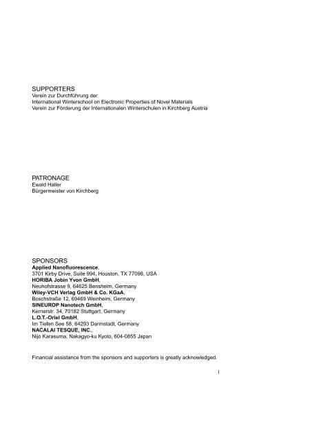
The NS1 Nanospectralyzer<br />
Automatic Fluorimetric Analysis of SWNTs<br />
n<br />
n<br />
n<br />
n<br />
n<br />
n<br />
n<br />
n<br />
n<br />
Rapid near-IR-fluorescence<br />
<strong>and</strong> absorption Spectroscopy<br />
Trace detection capability<br />
Three lasers, compact design<br />
Small sample volumes<br />
Sophisiticated versatile software<br />
Automatic display of (n, m)<br />
distributions in seconds<br />
Turn-key system operation<br />
Support from pioneering nanotube<br />
spectroscopists<br />
Generous software updates<br />
reflect new research findings<br />
Applied Nanofluorescence, LLC<br />
3701 Kirby Drive<br />
Houston, TX 77098 USA<br />
6,1<br />
5,3<br />
7,0<br />
6,2<br />
5,4<br />
8,0<br />
7,2<br />
6,4<br />
8,1<br />
7,3<br />
6,5<br />
9,1<br />
8,3<br />
7,5<br />
10,0 11,0<br />
9,2 10,2<br />
8,4<br />
7,6<br />
11,1 12,1<br />
10,3 11,3<br />
9,4<br />
8,6<br />
9,5 10,5<br />
8,7<br />
12,2 13,2<br />
11,4 12,4<br />
9,7<br />
armchair<br />
10,6 11,6<br />
9,8 10,8<br />
zigzag<br />
13,0 14,0 16,0<br />
14,1 15,1<br />
13,3 14,3<br />
12,5 13,5<br />
11,7 12,7<br />
10,9 11,9<br />
www.appliednanofluorescence.com<br />
15,2<br />
14,4<br />
13,6<br />
12,8<br />
11,10<br />
Lamp Sample<br />
Laser 1<br />
Laser 2<br />
Laser 3<br />
www.LOT-Oriel.com/nano<br />
LOT-Oriel GmbH & Co. KG<br />
Im Tiefen See 58<br />
64293 Darmstadt, Germany<br />
Relative abundance<br />
0.30<br />
0.25<br />
0.20<br />
0.15<br />
0.10<br />
0.05<br />
Near-IR<br />
Spectrograph<br />
<strong>and</strong><br />
Detector array<br />
Average diameter 0.857 nm<br />
Dispersion 0.206 nm<br />
0.00<br />
0.7 0.8 0.9 1.0 1.1 1.2 1.3 1.4 1.5<br />
Nanotube diameter (nm)
Graphene I <strong>and</strong> quantum dots<br />
Monday, March 9<br />
8:30 – 9:30 B. v. Wees, NL<br />
Spin injection, transport <strong>and</strong> manipulation in graphene field<br />
effect transistors.<br />
9:30 – 10:00 Novoselov, UK<br />
Graphene: the magic of flat carbon<br />
10:00 – 10:30 Coffee break<br />
10:30 – 11:00 S. G. Louie, US<br />
Graphene <strong>and</strong> graphene superlattices: pseudospin, electronelectron<br />
<strong>and</strong> electron-phonon effects<br />
11:00 – 11:30 C. Attaccalite, ES<br />
Electron-phonon coupling in graphene<br />
11:30 – 12:00 F. Mauri, FR<br />
Stability, chemical structure, <strong>and</strong> Clar’s aromatic sextets of<br />
hydrogen-terminated graphene ribbons<br />
12:00 – 17:00 Mini Workshops<br />
17:00 – 18:30 Dinner<br />
18:30 – 19:00 M. S. Fuhrer, US<br />
Probing diffusive <strong>and</strong> ballistic transport in graphene<br />
19:00 – 19:30 C. Stampfer, CH<br />
Graphene quantum dots<br />
19:30 – 20:00 M. Rontani, IT<br />
Molecular states of correlated electrons in quantum dots<br />
20:00 – 21:00 Poster Session I – MON<br />
27
Monday, March 9<br />
28
Graphene I <strong>and</strong> quantum dots Monday, March 9<br />
8:30<br />
Spin injection, transport <strong>and</strong> manipulation in graphene field effect transistors.<br />
Bart van Wees<br />
Zernike Institute for Advanced Materials, University of Groningen, Groningen, The<br />
Netherl<strong>and</strong>s<br />
I will give an overview of our experiments on single graphene layer field effect<br />
devices with ferromagnetic contacts. The use of the so-called non-local geometry<br />
allowed a detailed investigation of various aspects of spin injection, spin transport<br />
<strong>and</strong> spin manipulation.<br />
We found that: a) Spins can be injected into graphene with an injection efficiency<br />
up to 35 percent [1]. b) Spins can be transported through the graphene with a spin<br />
relaxation length of about 1.5 micrometer. By applying a perpendicular magnetic<br />
field Hanle spin precession could be studied [2]. c) By applying a large DC electric<br />
field the transport of spins between injector <strong>and</strong> detector could be facilitated using<br />
carrier drift [3]. d) The spin relaxation was found to be slightly anisotropic, with<br />
spins perpendicular to the graphene plane relaxing faster than spins in the plane<br />
[4]. The potential of graphene for future spintronics applications will be discussed.<br />
[1] C. Jozsa et al., Phys. Rev. B Rap. Com. to be published,(cond-mat 0811-2960)<br />
[2] N. Tombros et al, Nature 448, 571 (2007) [3] C. Jozsa et al., Phys. Rev. Lett.<br />
100, 236603 (2008) [4] N. Tombros et al., Phys. Rev. Lett. 101, 046601 (2008)<br />
9:30<br />
Graphene: the magic of flat carbon<br />
Kostya Novoselov<br />
School of Physics & Astronomy, University of Manchester, Manchester, UK<br />
When one writes by a pencil, thin flakes of graphite are left on a surface. Some<br />
of them are only one angstrom thick <strong>and</strong> can be viewed as individual atomic planes<br />
cleaved away from the bulk. This strictly two dimensional material called graphene<br />
was presumed not to exist in the free state <strong>and</strong> remained undiscovered until the<br />
last year. In fact, there exists a whole class of such two-dimensional crystals. The<br />
most amazing things about graphene probably is that its electrons move with little<br />
scattering over huge (submicron) distances as if they were completely insensitive<br />
to the environment only a couple of angstroms away. Moreover, whereas electronic<br />
properties of other materials are commonly described by quasiparticles that obey<br />
the Schrödinger equation, electron transport in graphene is different: It is governed<br />
by the Dirac equation so that charge carriers in graphene mimic relativistic particles<br />
with zero rest mass. The very unusual electronic properties of this material<br />
as well as the possibility for itâs chemical modification make graphene a promising<br />
c<strong>and</strong>idate for future electronic applications.<br />
29
Monday, March 9 Graphene I <strong>and</strong> quantum dots<br />
10:30<br />
Graphene <strong>and</strong> graphene superlattices: pseudospin, electron-electron <strong>and</strong><br />
electron-phonon effects<br />
Steven G. Louie<br />
Department of Physics, University of California at Berkeley, <strong>and</strong> Materials Sciences<br />
Division, Lawrence Berkeley National Laboratory<br />
I discuss some recent theoretical results we obtained on the electronic <strong>and</strong> optical<br />
properties of graphene <strong>and</strong> graphene superlattices. The low-energy excitations<br />
in these carbon nanostructures, which are 2D massless Dirac fermions, exhibit a<br />
number of unexpected behaviors. We showed that, owing to the chiral nature (pseudospin)<br />
of the electronic states, the carrier dynamics in graphene exhibits anomalous<br />
anisotropy when subjected to an external periodic potential of nanometer dimensions<br />
(called graphene superlattices). Under appropriate conditions, these graphene<br />
superlattices are predicted to be electron supercollimators <strong>and</strong> new generation of<br />
massless Dirac fermions may be created. Our first-principles calculations revealed<br />
that electron-electron <strong>and</strong> electron-phonon interactions give rise to significant<br />
corrections to the quasiparticle b<strong>and</strong> velocity of graphene <strong>and</strong> that both are central<br />
to the underst<strong>and</strong>ing of the electron linewidths as measured in angle-resolved<br />
photoemission experiment. We also investigated the optical properties of single<strong>and</strong><br />
bi-layer graphene with many-electron effects included. Although these systems<br />
are semimetals, excitonic effects are found to be quite significant in their optical<br />
absorption spectrum.<br />
11:00<br />
Electron-phonon coupling in graphene<br />
Claudio Attaccalite<br />
Unidad de Fisica de Materiales, Universidad del Pais Vasco, San Sebastian<br />
We studied the effect of electron-electron correlation on the full three dimensional<br />
dispersion of the π-b<strong>and</strong>s, Fermi velocities <strong>and</strong> effective masses of graphite/graphene.<br />
The results are then compared with recent experiments obtained by<br />
angle resolved photo-emission spectroscopy, <strong>and</strong> we found that the b<strong>and</strong> structure<br />
obtained by density-functional theory (in LDA approximation) strongly underestimates<br />
the slope of the b<strong>and</strong>s.Successively we investigate the effect of electronic<br />
correlation on the electron-phonon coupling (EPC) using different approximations,<br />
ranging from Hartree-Fock to GW. We found that GW renormalize the EPC at<br />
the A’1 K mode by almost 80% with respect to density functional theory in LDA<br />
approximation. The obtained phonon slope of the A’1 K is almost two time larger<br />
than the LDA one, in agreement with phonon dispersions from inelastic x-ray<br />
scattering <strong>and</strong> Raman spectroscopy experiments.<br />
30
Graphene I <strong>and</strong> quantum dots Monday, March 9<br />
11:30<br />
Stability, chemical structure, <strong>and</strong> Clar’s aromatic sextets of hydrogen-terminated<br />
graphene ribbons<br />
Francesco Mauri 1 Tobias Wassmann 1 Ari P. Seitsonen 1 A. Marco Saitta 1 M. Lazzeri<br />
1<br />
1 IMPMC, Universite Pierre et Marie Curie - Paris 6, Paris<br />
We determine the stability, the geometry, the electronic, <strong>and</strong> magnetic structure<br />
of hydrogen-terminated graphene-nanoribbon edges as a function of the hydrogen<br />
content of the environment by means of density functional theory [1]. Antiferromagnetic<br />
zigzag ribbons are stable only at extremely low ultravacuum pressures.<br />
Under more st<strong>and</strong>ard conditions, the most stable structures are the mono- <strong>and</strong><br />
dihydrogenated armchair edges <strong>and</strong> a zigzag edge reconstruction with one di- <strong>and</strong><br />
two monohydrogenated sites. At high hydrogen concentration âbulkâ graphene is<br />
not stable <strong>and</strong> spontaneously breaks to form ribbons, in analogy to the spontaneous<br />
breaking of graphene into small-width nanoribbons observed experimentally<br />
in solution. The stability <strong>and</strong> the existence of exotic edge electronic states <strong>and</strong>/or<br />
magnetism is rationalized in terms of Clarâs aromatic sextets.<br />
[1] T. Wassmann, A.P. Seitsonen, A.M. Saitta, M. Lazzeri, <strong>and</strong> F. Mauri, Phys.<br />
Rev. Lett. 101, 096402 (2008)<br />
31
Monday, March 9 Graphene I <strong>and</strong> quantum dots<br />
18:30<br />
Probing diffusive <strong>and</strong> ballistic transport in graphene<br />
Michael S. Fuhrer<br />
Department of Physics, University of Maryl<strong>and</strong>, College park<br />
I will discuss experiments performed on atomically-clean[1] graphene on SiO2 in<br />
ultra-high vacuum to determine the electron scattering rates from charged impurities[2],<br />
point defects[3], <strong>and</strong> phonons (graphene acoustic phonons <strong>and</strong> substrate<br />
polar optical phonons)[4]. The experiments point out both the promise of graphene<br />
as well as the technological challenges that lie ahead in realizing better samples. I<br />
will also discuss briefly experiments in the ballistic transport limit in few-100 nm<br />
single-layer (bi-layer) graphene samples, in which charge transport is dominated by<br />
resonant transmission of massless (massive) particle-in-a-box like states confined<br />
between the source <strong>and</strong> drain electrodes[5].<br />
[1] M. Ishigami, J. H. Chen, W. G. Cullen, M. S. Fuhrer, <strong>and</strong> E. D. Williams, Nano<br />
Letters 7, 1643 (2007).<br />
[2] J. H. Chen, C. Jang, M. S. Fuhrer, E. D. Williams, <strong>and</strong> M. Ishigami, Nature<br />
Physics, 4, 377 (2008).<br />
[3] C. Jang, S. Adam, J.-H. Chen, E. D. Williams, S. Das Sarma, M. S. Fuhrer,<br />
Physical Review Letters 101, 146805 (2008).<br />
[4] J. H. Chen, C. Jang, S. Xiao, M. Ishigami, M. S. Fuhrer, Nature Nanotechnology<br />
3, 206 (2008).<br />
[5] S. Cho <strong>and</strong> M. S. Fuhrer, submitted.<br />
32
Graphene I <strong>and</strong> quantum dots Monday, March 9<br />
19:00<br />
Graphene quantum dots<br />
Christoph Stampfer 1 Johannes Güttinger 1 Tobias Frey 1 Stephan Schnez 1 Françoise<br />
Molitor 1 Sarah Hellmüller 1 Thomas Ihn 1 Klaus Ensslin 1<br />
1 Nanophysics Group, ETH Zurich, Zurich<br />
Graphene, the first real two-dimensional solid consisting of a hexagonal lattice of<br />
carbon atoms reveals a number of unique electronic properties making this material<br />
interesting for high mobility electronics, spintronics <strong>and</strong> nanoelectronics in general.<br />
Here we report on measurements showing that excited single-particle states can be<br />
detected in graphene quantum dots via co-tunneling in the Coulomb blockade as<br />
well as via related conductance resonances at high voltage bias outside the blockaded<br />
regions. The devices, consisting of graphene isl<strong>and</strong>s with diameters of around<br />
50 to 140 nanometers are connected via two narrow graphene constrictions to source<br />
<strong>and</strong> drain contacts. These devices are tunable by lateral graphene gates. From<br />
transport measurements we extract charging energies around 10 meV <strong>and</strong> singlelevel<br />
spacings of a few meV. We demonstrate the functionality of a charge-read-out<br />
using a nearby graphene constriction. Both steps, the detection of excited states <strong>and</strong><br />
the charge-read-out, are crucial for the investigation of graphene quantum devices<br />
in general as well as for future implementations of spin qubits in graphene.<br />
33
Monday, March 9 Graphene I <strong>and</strong> quantum dots<br />
19:30<br />
Molecular states of correlated electrons in quantum dots<br />
Massimo Rontani<br />
CNR-INFM Research Center S3, Modena, Italy<br />
The electron-electron interaction is predicted to fundamentally affect electron states<br />
in quantum dots (QDs), giving rise -in certain regimes- to a molecule made of electrons,<br />
whose mutual distances are rigidly fixed like those of nuclei in conventional<br />
molecules.<br />
We first report evidence of molecular behavior based on inelastic light scattering<br />
measurements of the excitations of low-density GaAs quantum dots containing exactly<br />
four electrons. Theoretical predictions obtained via the configuration interaction<br />
(CI) method are in quantitative agreement with the observed excitations <strong>and</strong><br />
highlight that roto-vibrational modes develop at the onset of short-range correlation.<br />
We then investigate QDs in carbon nanotubes, which provide dramatic evidence of<br />
correlation. Our CI calculations take into account the role of two-valley degeneracies<br />
as well as the spin-orbit interaction. Without spin-orbit, the two-electron ground<br />
state is a triplet, due to the occurrence of a pseudospin degree of freedom linked<br />
to the orbital degeneracy. By including spin-orbit, we demonstrate that Coulomb<br />
correlation is an essential feature for explaining recent single-electron tunnelling<br />
spectra.<br />
34
Monday, March 9 Graphene I <strong>and</strong> quantum dots<br />
38
Poster session Monday, March 9<br />
1<br />
New NMR strategies to study carbon nanotubes<br />
Edy Abou-Hamad 1 Y. Kim 2 T. W˚agberg 3 A. Rubio 4 D. E. Luzzi 2 C. Goze-Bac 1<br />
1 Laboratoire Colloïdes, Verres et Nanomatériaux, CNRS Université Montpellier 2,<br />
France<br />
2 Department of Materials Science <strong>and</strong> Engineering, University of Pennsylvania,<br />
Philadelphia, PA, USA<br />
3 Department of Physics, Ume˚a University, S-901 87 Ume˚a, Sweden<br />
4 European Theoretical Spectroscopy Facility (ETSF), Dpto. Física de Materiales<br />
<strong>and</strong> Centro Mixto CSIC-UPV/EHU, Universidad del País Vasco UPV/EHU, Edificio<br />
Korta, Avd. Tolosa 72, 20018 San Sebastián, Spain<br />
The local magnetic properties of the one dimensional inner space of the nanotubes<br />
are investigated using 13 C nuclear magnetic resonance spectroscopy of encapsulated<br />
fullerene molecules inside single walled carbon nanotubes. Isotope engineering<br />
<strong>and</strong> magnetically purified nanotubes have been advantageously used on our study<br />
to discriminate between the different diamagnetic <strong>and</strong> paramagnetic shifts of<br />
the resonances. Ring currents originating from the π electrons circulating in the<br />
nanotube, are found to actively screen the applied magnetic field by -36.9 ppm.<br />
Defects <strong>and</strong> holes in the nanotube walls cancel this screening locally. At high magnetic<br />
fields, the modifications of the NMR resonances of the molecules from free to<br />
encapsulated can be exploited to determine some structural characteristics of the<br />
surrounding nanotubes.<br />
2<br />
Helicities sorting of single-walled carbon nanotubes by amphiphiles molecules<br />
adsorption studied by resonant Raman excitation profiles<br />
L. Alvarez 1 A. Righi 2 I. O. Maciel 2 M. A. Pimenta 2 T. Michel 1 J. L. Sauvajol 1 R.<br />
Marquis 3 S. Meunier 3<br />
1 LCVN, University Montpellier II, UMR 5587 France<br />
2 Departamento de Física, Universidade Federal de Minas Gerais, Belo Horizonte,<br />
MG, 30123-970, Brazil<br />
3 Laboratoire de Synthése Bioorganique UMR 7175 - LC1 Faculte de Pharmacie BP<br />
24 67 401 ILLKIRCH- France<br />
Adsorption of specifically designed polyaromatic amphiphiles were used to sort<br />
single-walled carbon nanotubes (SWNTs) with different helicities. The sorting is<br />
investigated by resonant Raman excitation profiles. Chiral indexes (n <strong>and</strong> m) of<br />
SWNTs present in our samples are determined by fitting the Raman peaks observed<br />
in the radial breathing modes region (RBM). Scanning over an excitation<br />
energy range between 2 <strong>and</strong> 2.2 eV with a 0.01 eV step allows to investigate mainly<br />
two families of metallic nanotubes (2n+m=24 <strong>and</strong> 2n+m=27). The results display<br />
significant differences between the sorted <strong>and</strong> the reference samples, meaning that<br />
39
Monday, March 9 Poster session<br />
discrimination between SWNTs of different helicities is possible.<br />
3<br />
Improving Quality of Single Walled Carbon Nanotube Networks<br />
Alberto Ansaldo 1 S<strong>and</strong>esh Jaybhaye 1,2 Marco Chiarolini 3 Ermanno Di Zitti 3 Davide<br />
Ricci 1<br />
1 Istituto Italiano di Tecnologia, Via Morego 30, I-16163 Genova â Italy<br />
2 Nanotechnology Research Center, Birla College, Kalyan, 421304, Maharashtra â<br />
India<br />
3 Dipartimento di Ingengeri Biofisica ed Elettronica, Universitá di Genova,<br />
Via Opera Pia 11a, I-16145 Genova â Italy<br />
Single walled carbon nanotubes (SWCNTs) are one of the most interesting materials<br />
for transparent conductive films. SWCNT percolating networks have been<br />
produced by a variety of different methods mainly by spraying <strong>and</strong> filtration. Unfortunately,<br />
suspending CNTs in liquid requires the use of ultrasound <strong>and</strong> surfactants.<br />
Sonication reduces bundling but increases the number of defects <strong>and</strong> shortens CNT<br />
length. Moreover, after deposition, surfactants are difficult to be removed <strong>and</strong> tend<br />
to create an insulating layer between CNTs <strong>and</strong> between CNTs <strong>and</strong> contacts. The<br />
overall effect is to considerably reduce the global conductivity of CNT films. It is<br />
our opinion that a considerable improvement in film quality could come from a direct<br />
synthesis of the network by chemical vapour deposition (CVD) <strong>and</strong> combining<br />
this with direct transfer techniques that avoid suspension of the CNTs in a liquid.<br />
In this work we show our latest results in enhancing the quality of SWCNT percolating<br />
network synthesis by alcohol CVD on silicon oxide substrates using cobalt <strong>and</strong><br />
nickel acetates as precursors, varying catalyst composition, substrate preparation<br />
<strong>and</strong> catalyst pre-treatment.<br />
4<br />
Engineering the spin transport in graphene with vacancies<br />
Vasilii I. Artyukhov 1 Leonid A. Chernozatonskii 1<br />
1 Institute of Biochemical Physics RAS, Moscow<br />
We use densiy functional theory to study in detail the magnetic structure of monovacancies<br />
in graphene. Breaking of sublattice symmetry leads to spin polarization,<br />
coming from both localized <strong>and</strong> delocalized states. We propose arranging the vacancies<br />
in one-dimensional ’tracks’ as a pathway to create novel spintronic circuit<br />
elements with highly tunable properties, based entirely on graphene. We also study<br />
the effects of chemical modification of vacancies with different species (H, F, B, N)<br />
to saturate the reactive dangling bonds; controlled cemical modification is proposed<br />
as an additional tool to alter the magnetic structure of graphene.<br />
5<br />
40
Poster session Monday, March 9<br />
Continuum Elastic Modeling of Graphene Resonators<br />
Juan Atalaya 1 Andreas Isacsson 1 Jari M. Kinaret 1<br />
1 Department of Applied Physics, Chalmers University of Technology, Sweden.<br />
Starting from an atomistic approach, we have derived a hierarchy of successively<br />
more simplified continuum elasticity descriptions for modeling the mechanical<br />
properties of suspended graphene sheets. We find that already for deflections of the<br />
order of 0.5 ˚A a theory that correctly accounts for nonlinearities is necessary <strong>and</strong><br />
that for many purposes a set of coupled Duffing-type equations may be used to<br />
accurately describe the dynamics of graphene membranes. The descriptions are validated<br />
by applying them to square graphene-based resonators with clamped edges<br />
<strong>and</strong> studying numerically their mechanical responses. Both static <strong>and</strong> dynamic responses<br />
are treated, <strong>and</strong> we find good agreement with recent experimental findings.<br />
41
Monday, March 9 Poster session<br />
6<br />
Photoemission <strong>and</strong> x-ray absorption studies on magnetic rare earth metallofullerenes<br />
<strong>and</strong> ErCl3 nanowires inside carbon nanotube templates<br />
Paola Ayala1 Ryo Kitaura2 Hidetsugu Shiozawa3 Hisanori Shinohara2 David Batchelor4<br />
Esko Kauppinen1 Christian Kramberger5 Thomas Pichler5 1Department of Applied Physics, Helsinki University of Technology, Finl<strong>and</strong><br />
2Department of Chemistry <strong>and</strong> Institute for Advanced Research, Nagoya University,<br />
Japan<br />
3Department of Electronic Engineering, University of Surrey, UK<br />
4BESSY II,Berlin, Germany<br />
5Faculty of Physics, University of Vienna, Austria<br />
Magnetic rare earth metallofullerenes <strong>and</strong> crystalline ErCl3 nanowires templated<br />
inside carbon nanotubes can be tailored under high temperature <strong>and</strong> vacuum with<br />
a high filling-ratio yielding novel magnetic chains <strong>and</strong> quantum wires [1,2]. A combination<br />
of resonant photoemission <strong>and</strong> XAS has been utilized to assess the charge<br />
transfer <strong>and</strong> bonding environment in the pristine nanotube templates <strong>and</strong> the filled<br />
functionalized separated samples [3]. Core level information of the filler is investigated<br />
to reveal hybridization state <strong>and</strong> bonding environment of the elements in<br />
these structures. Resonant PES is also studied in order to discern the metallicity<br />
of the filler. This allows us to evaluate the changes in the electronic structure of<br />
the valence <strong>and</strong> conduction b<strong>and</strong> of the CNT. For the latter additionally, XPS line<br />
shape analysis will also be discussed for a detailed analysis of the chemical state<br />
<strong>and</strong> bonding environment.<br />
Work supported by the DFG PI 440 3/4/5.<br />
[1] R.Kitaura <strong>and</strong> H.Shinohara, Jap.J.Appl.Phys.46 (2007) 881<br />
[2] R.Kitaura et al. NanoRes 1(2008)152<br />
[3] T.Pichler et al. Phys.Stat.Sol.b 245(2008) 2038<br />
7<br />
Carbon Nanotube Synthesis via Ceramics<br />
A. Bachmatiuk1 M. Bystrzejewski2 P. Ayala3 F. Schaeffel1 E. Borowiak-Palen4 A. Huczko2 H. Lange2 T. Gemming1 T. Pichler5 C. Mickel1 R. Klingeler1 H-W.<br />
Hübers6 M. H. Rümmeli1 1Leibniz Institute for Solid State <strong>and</strong> Materials Research Dresden, Germany<br />
2Warsaw University, Dept of Chemistry, 02-093 Warsaw, Pol<strong>and</strong><br />
3Laboratory of Physics <strong>and</strong> Center for New Materials, Helsinki University of Technology,<br />
Finl<strong>and</strong><br />
4Szczecin University of Technology, KnowMatTech, Szczecin, Pol<strong>and</strong><br />
5Department of Physics, Vienna University, Strudlhofgasse 4, A-1090 Wien, Au-<br />
stria<br />
6 German Aerospace Agency (DLR), Adlershof, Berlin, Germany<br />
42
Poster session Monday, March 9<br />
The potential for ceramics as catalysts for CNT formation exceeds that from metal<br />
catalysts in that ceramics can serve as a catalyst particle for CNT nucleation/growth<br />
as found with metal catalysts. In addition, they can also serve as a<br />
template for the synthesis of carbon nanostructures. This latter point (template<br />
route) provides a more versatile means to engineer different types of nanotubes<br />
structures (e.g. Y junctions), as compared to metals catalysts. Furthermore, ceramics<br />
are often removed (purification) from as produced samples far more easily than<br />
metal catalysts. Here we present studies on the growth of carbon nanotubes (CNT)<br />
from ceramics in chemical vapour deposition (CVD) <strong>and</strong> laser pyrolysis routes. We<br />
show CNT growth from both ceramic particles <strong>and</strong> nanowires. The nanowires serve<br />
as templates. Further, we demonstrate the templating route can also be used for<br />
doping (B) the CNT.<br />
8<br />
Solubilization <strong>and</strong> Density Gradient Fractioning of SWCNTs by a Novel three<br />
Component Surfactant Class Based on Perylene Dyes<br />
Claudia Backes 1 Cordula D. Schmidt 2 Frank Hauke 1 Andreas Hirsch 2<br />
1 Institute of Advanced Materials <strong>and</strong> Processes, University Erlangen Nurenberg<br />
2 Department of Chemistry <strong>and</strong> Pharmacy, University Erlangen Nurenberg<br />
For exfoliating SWNTs, we have developed a three component surfactant with<br />
solvophylic moiety, polycyclic aromatic perylene bisimide unit for interaction with<br />
the SWNT backbone <strong>and</strong> hydrophobic aliphatic tail. The degree of individualization<br />
of the SWNTs is higher than for dispersions in the commonly used surfactant<br />
SDBS as shown by statistical AFM analysis. Furthermore, optical spectroscopy revealed<br />
dispersion <strong>and</strong> individualization at a SWNT to perylene (Per) weight ratio<br />
of 2:1. The SWNT-Per dispersions were characterized by various spectroscopic <strong>and</strong><br />
microscopic techniques. A π -stacking interaction is reflected by a redshift of the optical<br />
perylene transitions, a strong alteration of the SWNT emission pattern <strong>and</strong> a<br />
significant quenching of the SWNT <strong>and</strong> perylene fluorescence intensity (C. Backes,<br />
et. al., J. Am. Chem. Soc., accepted).<br />
We have applied this surfactant in density gradient ultracentrifugation (DGU) separation<br />
experiments where a high degree of SWNT individualization is a key to<br />
success. SWNTs were fractioned in a combined co-surfactant <strong>and</strong> replacement DGU<br />
approach underlining the versatility of our dispersion concept (C. Backes, et. al.,<br />
Chem. Commun., accepted).<br />
43
Monday, March 9 Poster session<br />
9<br />
Carbon Nanotube CVD on a Tantalum support for Interconnect Fabrication â<br />
materials interactions<br />
B. C. Bayer 1 C. Castellarin-Cudia 2 A. Goldoni 2 C. Cepek 3 S. Hofmann 1 J. Robertson<br />
1<br />
1 Engineering Department, University of Cambridge, Cambridge, UK<br />
2 Sincrotrone Trieste S.c.p.A., Area Science Park, Trieste, Italy<br />
3 Laboratorio Nazionale TASC-CNR-INFM, Trieste, Italy<br />
A possible application for carbon nanotubes (CNTs) is the use as interconnects<br />
in large scale integrated (LSI) circuits [1]. However, the deposition process must<br />
yield vertically aligned, high density CNTs on conductive materials <strong>and</strong> must be<br />
compatible with commonly used LSI materials.<br />
In this study we examine the growth of CNTs by thermal chemical vapour deposition<br />
(CVD) on LSI-compatible Ta support layers with an iron catalyst. Structural<br />
<strong>and</strong> morphological characterisation of the obtained CNT forests <strong>and</strong> the support/catalyst<br />
system is undertaken to gain insight into possibly growth-inhibiting<br />
reactions of the Ta support layer, the metal catalyst layer, the process gases <strong>and</strong><br />
residual gases in the CVD system <strong>and</strong> their temperature dependence. In addition,<br />
X-ray photoelectron spectroscopy (XPS) is used to resolve chemical interactions<br />
directly at the interface of the buffer layer, the catalyst <strong>and</strong> the growing CNTs.<br />
This is compared to CNT growth on commonly used oxide supports [2].<br />
[1] Robertson J. et al., Appl Phys Lett, 93, 163111-1, 2008<br />
[2] Mattevi C. et al., J Phys Chem C, 112, 32, 12207, 2008<br />
10<br />
Multi Walled Carbon Nanotubes Plastic Actuator<br />
Maurizio Biso 1 Davide Ricci 2<br />
1 Dipartimento di Informatica Sistemistica e Telematica, Università di Genova,<br />
Via all’Opera Pia 13, I-16145 Genova â Italy<br />
2 Istituto Italiano di Tecnologia, Via Morego 30, I-16163 Genova â Italy<br />
Carbon nanotubes have electrical <strong>and</strong> mechanical properties that make them highly<br />
attractive for actuators. They have the ability to deform elastically by several<br />
percent, thus storing very large amounts of energy, thanks to their crystalline nature<br />
<strong>and</strong> to their morphology. A bimorph actuator composed of single walled carbon<br />
nanotubes (SWCNTs), polyvinylidene difluoride (PVDF) <strong>and</strong> the ionic liquid<br />
(IL) 1-butyl 3-methylimidazolium tetrafluoroborate [BMIM][BF4] with a polymersupported<br />
internal ionic liquid electrolyte was previously demonstrated by Aida<br />
et al. [1] . While several experiments were carried on using SWCNTs, PVDF <strong>and</strong> a<br />
number of ILs, the use of multi walled carbon nanotubes instead of SWCNTs is,<br />
to our knowledge, a new result that will be presented here. Electrochemical cha-<br />
44
Poster session Monday, March 9<br />
racterizations by cyclic voltammetry, impedance spectroscopy <strong>and</strong> actuation tests<br />
performed applying a square wave of 4 Volt peak-to-peak at frequencies between<br />
0.3 Hz <strong>and</strong> 2 Hz will be reported <strong>and</strong> discussed.<br />
[1] T.Fukushima, T.Aida, âIonic Liquids for Soft Functional Materials with Carbon<br />
Nanotubes,â C hem.Eur.J., vol. 13, no.18, pp. 5048-5058, Jun. 2007<br />
11<br />
Strongly Correlated Electron Phenomena in Carbon Nanotubes<br />
Marc Bockrath 1 Vikram V. Deshp<strong>and</strong>e 1 Bhupesh Ch<strong>and</strong>ra 2 Robert Caldwell 2 Dmitry<br />
Novikov 3 James Hone 2<br />
1 California Institute of Technology, Pasadena<br />
2 Columbia University, New York<br />
3 Yale University, New Haven<br />
In this talk I will discuss our recent results demonstrating strongly correlated electron<br />
behavior in ultra-clean carbon nanotube quantum dots. Specifically, we have<br />
observed one-dimensional (1D) Wigner crystal behavior of dilute holes in semiconducting<br />
nanotubes, finding three distinct regimes of spin <strong>and</strong> valley quantum<br />
number ordering as the charge density <strong>and</strong> axial magnetic field are varied. The<br />
boundaries between the regimes in density <strong>and</strong> magnetic field are well-described<br />
by the theory of Levitov <strong>and</strong> Tsvelik for a narrow-gap Luttinger liquid. In the<br />
second part of the talk I will present results showing that the electrons in nominally<br />
metallic nanotubes comprise a 1D Mott insulator. This indicates that carbon<br />
nanotubes are never truly metallic, in agreement with theoretical predictions that<br />
account for umklapp scattering at half-filling due to electron-electron interactions.<br />
Using inelastic cotunneling spectroscopy, we also observe neutral electronic excitations<br />
within the gap, yielding an additional signature of strong electron-electron<br />
interactions. Our results demonstrate nanotubes’ promise for studying a variety of<br />
tunable correlated electron phenomena in 1D.<br />
12<br />
Tailoring carbon nanotubes grown from non-ferromagnetic catalysts via CVD.<br />
Ewa Borowiak-Palen 1 A. Steplewska 1 A. Bachmatiuk 1 M. H. Rümmeli 2 R. J. Kalenczuk<br />
1<br />
1 Institute of Chemical <strong>and</strong> Environment Engineering, Szczecin University of Tech-<br />
nology, Szczecin<br />
2 2. Leibniz Institute of Solid State <strong>and</strong> Materials Research Dresden, Germany<br />
The catalytic growth of different carbon nanotubes by chemical vapor deposition<br />
(CVD) using non-ferromagnetic catalyst particles (such as copper) will be presented.<br />
In this work detailed studies that catalysts with fully filled d orbital (e.g. Cu)<br />
can be a source of bulk scale synthesis of singlewalled or multiwalled carbon nano-<br />
45
Monday, March 9 Poster session<br />
tubes using the same catalyst mix ( viz. equal molar ratio of metal to magnesia)<br />
but with different experimental setups <strong>and</strong> conditions. The detailed analysis of the<br />
samples is supported by electron transmission microscopy observations, energy dispersive<br />
X-Ray spectroscopy mode, X-Ray Diffraction <strong>and</strong> Raman spectroscopy.<br />
13<br />
Various methods of surface-enhanced Raman spectroscopy applied to single<br />
<strong>and</strong> double walled carbon nanotubes<br />
Bea Botka 1 Katalin Kamaras 1<br />
1 Research Intitute for Solid State Physics <strong>and</strong> Optics, Budapest<br />
We investigated several SERS (surface-enhanced Raman spectroscopy) methods<br />
reported in the literature regarding their application to carbon nanotubes. Silver<br />
<strong>and</strong> gold were used to prepare different types of surfaces. We achieved surface enhancement<br />
factors up to 200 by a modification of the method by Ouyang <strong>and</strong> Fang<br />
[1] on silver. In particular, we were able to detect with enhanced sensitivity the<br />
intermediate frequency modes (Z-breathing phonons), which correspond to vibrations<br />
along the nanotube axis, <strong>and</strong> which, according to theoretical predictions [2],<br />
are sensitive to the nanotube length. These modes are usually weak or non-existent<br />
in the normal Raman spectra. We will compare these modes in several types of<br />
nanotube samples, <strong>and</strong> demonstrate the effect of physical <strong>and</strong> chemical treatment.<br />
Supported by the European Commission FP7 through the Initial Training Network<br />
FINELUMEN, contract PITN-GA-2008-215399.<br />
[1] Y. Ouyang, Y. Fang: Spectrochimica Acta Part A 61 (2005) 2211â2213<br />
[2] R. Saito et al. : Phys. Rev. B 59 (1999) 2388-2392<br />
14<br />
Polarized Raman measurements on the reaction center of crystallized photosystem<br />
II<br />
Katharina Brose 1 Athina Zouni 2 Matthias Broser 2 Janina Maultzsch 1<br />
1 Festkörperphysik, Technische Universität Berlin, Berlin<br />
2 Institut für Chemie, Technische Universität Berlin, Berlin<br />
In photosynthesis the sunlight is collected by antenna pigments <strong>and</strong> transmitted<br />
to special molecule structures called photosystem I <strong>and</strong> photosystem II, where the<br />
energy of light is transformed into a separation of charge. In the photosystem II<br />
reaction center, two β-carotene molecules CarD1 <strong>and</strong> CarD2 were identified, which<br />
are oriented perpendicular to each other 1 . The role of these carotenes in the pho-<br />
46
Poster session Monday, March 9<br />
tosynthesis process is still unknown. We use Raman spectroscopy, which is one<br />
of the most important methods to analyse the structure of solids <strong>and</strong> molecules,<br />
to study the two β-carotenes. We present polarized Raman measurements of the<br />
beta-carotene vibrational modes in single crystals of photosystem II <strong>and</strong> discuss the<br />
possible origin of the observed polarization dependence.<br />
15<br />
A Molecular 15 N Quantum Nuclear Memory using 15 N@C60<br />
Richard M. Brown 1 John J. L. Morton 1 Alexei M. Tyryshkin 2 Kyriakos Porfyrakis 1<br />
Arzhang Ardavan 3 G. Andrew D. Briggs 1 S. A. Lyon 2<br />
1 University of Oxford, Oxford<br />
2 Department of Electrical Engineering, Princeton University, Princeton, NJ 08544,<br />
USA.<br />
3 Clarendon Laboratory, Department of Physics, Oxford University, Oxford, OX1<br />
3PJ, UK<br />
N@C60 is of significant interest in the quantum information processing (QIP) community<br />
due to its long electron decoherence times <strong>and</strong> ability to be incorporated<br />
into larger computing architectures. In QIP the loss of information through the<br />
process of decoherence is a fundamental problem, but it can be combated through<br />
the transfer of qubit (quantum bit) states. Electron spins allow fast manipulation<br />
<strong>and</strong> are easily initialised compared to nuclear spins, but suffer from short decoherence<br />
times. Nuclear spins have significantly larger decoherence times than electron<br />
spins <strong>and</strong> hence propagation of states can provide a route to information storage.<br />
Thus, a powerful model would use the electron qubit for initialisation, processing<br />
<strong>and</strong> readout, with transfer to a nuclear ‘memory’ qubit. We have implemented such<br />
a scheme using a series of tuned microwave <strong>and</strong> radiofrequency pulses to produce<br />
a 15 N nuclear memory within a dilute 15 N@C60 in C60 matrix. The work reports<br />
a significant improvement in decoherence time of over two orders of magnitude<br />
through information transfer from the electron to the nuclear spin state, with a<br />
two-way fidelity of 70%.<br />
16<br />
COMPARATIVE STUDY OF THE ELECTRONIC STRUCTURE OF DIFFERENT<br />
TYPES OF SINGLE-WALL CARBON NANOTUBES<br />
Lyubov G. Bulusheva1 Alex<strong>and</strong>er A. Okotrub1 Yuliya V. Lavskaya1 Mikhail A. Kanygin1<br />
Kenji Hata2 Urszula Dettlaff-Weglikowska3 Antonio Fonseca4 1Nikolaev Institute of Inorganic Chemistry, Novosibirsk, Russia<br />
2AIST, Tsukuba, Japan<br />
3Max-Planck-Institute for Solid State Research, Stuttgart, Germany<br />
4Laboratoire de Chimie et dâElectrochimie des Surfaces, FUNDP, Namur, Belgium<br />
Electronic structure of single-wall carbon nanotubes (SWNTs) has been probed<br />
47
Monday, March 9 Poster session<br />
by near-edge X-ray absorption fine structure (NEXAFS) spectroscopy. Three types<br />
of SWNT samples were examined: SWNTs produced by laser vaporization method,<br />
SWNTs synthesized by methane decomposition over Co catalyst supported<br />
on MgO, <strong>and</strong> aligned SWNTs produced on silicon support using a super-growth<br />
method. Alignment of the third type of SWNTs was determined from an angular<br />
dependence of a ratio of π* <strong>and</strong> σ* resonances. The width of angular distribution of<br />
SWNTs in a film exceeds the value found from SEM image analysis that could be<br />
due to defects in SWNTs. Defects should contribute to the NEXAFS spectrum <strong>and</strong><br />
we found that π* resonance width has the smaller value for laser-produced SWNTs<br />
<strong>and</strong> the larger value for aligned SWNTs. X-ray absorption spectra of armchair, zigzag<br />
<strong>and</strong> semiconducting chiral carbon nanotubes were modeled based on the results<br />
of B3LYP calculations. It was shown that the geometry of carbon nanotubes has<br />
effect on the width of the π* resonance. Thus, NEXAFS spectroscopy could be used<br />
for checking of a presence of metallic SWNTs in a sample.<br />
17<br />
Characterisation of cobalt(II)porphyrin/carbon nanotube nanohybrids by electron<br />
paramagnetic resonance <strong>and</strong> optical spectroscopy<br />
Sofie Cambré1 Wim Wenseleers1 Jelena Čulin2 Sabine Van Doorslaer3 Etienne Goovaerts1<br />
1Experimental Condensed Matter Physics Laboratory, University of Antwerp (Belgium),<br />
Antwerp<br />
2Rudjer Boskovic Institute (Croatia), 1000 Zagreb<br />
3Spectroscopy in Biophysics <strong>and</strong> Catalysis Laboratory, University of Antwerp (Bel-<br />
gium), Antwerp<br />
In this study, we use electron paramagnetic resonance (EPR) spectroscopy in combination<br />
with absorption, steady state <strong>and</strong> time resolved fluorescence spectroscopy to<br />
characterize paramagnetic cobalt(II)octaethylporphyrin (CoOEP)/single-wall carbon<br />
nanotube (SWNT) nanohybrids.[1] While measuring on a bulk sample, two<br />
different components can be distinguished in the EPR spectrum, arising from porphyrins<br />
interacting with metallic <strong>and</strong> semiconducting NTs. From analysing these<br />
two EPR contributions, we conclude that the metallic NTs are stronger π-acceptors<br />
for the porphyrins than the semiconducting NTs. Solubilising the nanohybrids in<br />
water using bile salt surfactants[2], after applying a thorough washing procedure,<br />
yields stable solutions in which at least 99% of the porphyrins are adsorbed on the<br />
NTs. Thanks to this purification, we observe the isolated absorption spectrum of<br />
the interacting porphyrins, which is strongly red-shifted compared to the free porphyrin<br />
absorption, <strong>and</strong> a quasi-complete quenching of the porphyrin fluorescence.<br />
[1] S. Cambré et al., ChemPhysChem 2008, 9, 1930 [2] W. Wenseleers et al., Adv.<br />
Funct. Mater. 2004, 14, 1107<br />
48
Poster session Monday, March 9<br />
18<br />
Manipulation of spin-active peapods for magnetic resonance studies<br />
S. Casimirius 1 L. Ciric 1 M. Duchamp 1 A. Magrez 1 J. H. Warner 2 H. Shinohara 2<br />
M. H. Rümmeli 3 G. A. D. Briggs 2 L. Forro 1<br />
1 Institute of Physics of Complex Matter, EPFL, Lausanne, Switzerl<strong>and</strong><br />
2 Department of Materials, Oxford University, Oxford, UK<br />
3 IFW Dresden, Helmholtzstr. 20, 01069 Dresden, Germany<br />
Fullerene-like materials open up new fields in spin electronics because of their intrinsic<br />
characteristics as well as their ability to host species. Peapods, produced from<br />
spin-bearing endohedral fullerenes, enable to study spin-spin interactions, <strong>and</strong> spin<br />
transfer along spin chain. Herein, we will report on the fabrication of peapod-based<br />
devices for spin-chain analysis by Electron Spin Resonance (ESR) <strong>and</strong> electrically<br />
detected magnetic resonance (EDMR) for investigation of spin-dependent transport<br />
properties. Peapods are synthesized by sublimation of metallofullerenes in presence<br />
of single-walled carbon nanotubes which are produced by laser-evaporation process<br />
with non-magnetic catalyst, <strong>and</strong> sorted by electronic structure. Then, peapods<br />
are deposited onto substrates from organic solvent based-suspensions of debundled<br />
materials. Individual species as well as thin films with controlled orientation of the<br />
peapods can be obtained by means of dielectrophoresis. Finally, the integration of<br />
La@C82 peapods by use of electron-beam lithography into probe devices designed<br />
for magnetic studies will be presented.<br />
19<br />
Improvement of Polypyrrole <strong>and</strong> Carbon Nanotube Co-deposition Techniques<br />
for High Charge-transfer Electrodes<br />
Elisa Castagnola 1 Maurizio Biso 1 Davide Ricci 2<br />
1 Dipartimento di Informatica Sistemistica e Telematica, Universitá di Genova,all<br />
2 Istituto Italiano di Tecnologia, Via Morego 30, I-16163 Genova â Italy<br />
Both carbon nanotubes (CNTs) <strong>and</strong> polypyrrole (PPy) have been investigated as<br />
materials for manufacturing high charge-transfer electrodes due to their outst<strong>and</strong>ing<br />
performances. The combination of the complementary properties of CNTs <strong>and</strong><br />
PPy via an electrochemical co-deposition route has been already shown to achieve<br />
interesting results. In this work, PPy <strong>and</strong> chemically-functionalized multi walled<br />
CNTs (COOH-MWCNT) were potentiostatically, galvanostatically <strong>and</strong> potentiodynamically<br />
electrodeposited from an aqueous solution at different temperatures<br />
to form a nanocomposite on the surface of a variety of metal electrodes. A study of<br />
the influence of experimental parameters such as temperature, current, <strong>and</strong> growth<br />
rate in the different electrodeposition methods was performed. The electronic <strong>and</strong><br />
electrochemical properties of the nanocomposite films have been studied by cyclic<br />
voltammetry <strong>and</strong> electrochemical impedance spectroscopy, while a morphological<br />
study has been performed via scanning electron microscopy. A comparison between<br />
49
Monday, March 9 Poster session<br />
the different techniques will be reported <strong>and</strong> guidelines for best results depending<br />
on the application will be discussed.<br />
20<br />
Atomic Diffusion <strong>and</strong> Reshaping of Solid Catalytic Particles During Nanotube<br />
Growth<br />
Felipe Cervantes-Sodi 1 G. Csányi 1 S. Piscanec 1 A. C. Ferrari 1<br />
1 Engineering Department, University of Cambridge, Cambridge<br />
The catalytic particle dynamics during catalytic chemical vapor deposition of nanotubes<br />
(CNTs) plays a fundamental role in the nucleation <strong>and</strong> growth process <strong>and</strong><br />
in the final CNT morphology. In-situ transmission electron microscopy videos at<br />
low temperatures show constantly reshaping solid catalytic particles [1,2]. Here, we<br />
explain the physics of this process <strong>and</strong> link it to the final CNT morphology. Using a<br />
combination of multiscale atomistic modeling <strong>and</strong> analytic continuum calculations<br />
we show that the reshaping can be either via surface diffusion or via bulk drift of the<br />
Ni atoms [3]. The temperature <strong>and</strong> the activity of the growing CNT edge determine<br />
the degree of surface diffusion or bulk drift. The nanoparticle reshaping is driven by<br />
capillary forces. The interplay between the capillary <strong>and</strong> anchoring forces can lead<br />
to either: 1)steady CNT growth, 2)encapsulation of the nanoparticle, 3)splitting of<br />
the nanoparticle, or 4)formation of bamboo-like CNTs. The physics in our study is<br />
elemental <strong>and</strong> general, <strong>and</strong> can be extrapolated to other nanosystems.<br />
1 S. Hofmann, et al. Nano Lett, 7 602 (2007)<br />
2 S. Helveg, et al. Nature, 427 426 (2004)<br />
3 F. Cervantes-Sodi et al submitted (2009)<br />
21<br />
METALLIC SINGLE-WALL CARBON NANOTUBES SEPARATED BY DENSITY<br />
GRADIENT ULTRACENTRIFUGATION<br />
Alex<strong>and</strong>er Chernov 1 Elena Obraztsova 1 Anatolii Lobach 2<br />
1 A.M. Prokhorov General Physics Institute, RAS, 38 Vavilov str., 119991, Moscow,<br />
Russia<br />
2 Institute of Problems of Chemical Physics, RAS, 142432, Chernogolovka, Russia<br />
Unique properties of single wall carbon nanotubes (SWNTs) are already successfully<br />
used in technologies. Depending on geometry SWNTs may be either metallic or<br />
semiconducting. Up to now synthesis is not able to provide a purely metallic nanotube<br />
fraction. A recent method of a density gradient ultracentrifugation (DGU)<br />
is efficient in separation of SWNTs. In this work we used DGU to extract a metallic<br />
fraction from as-grown arc-discharge SWNTs. The process parameters (the<br />
surfactant type <strong>and</strong> concentration, the treatment time, the approach to the gradient<br />
formation) have been optimized. The metallic fraction has appeared as an<br />
upper one, colored in blue. The fraction has been studied with the UV-VIS-NIR<br />
50
Poster session Monday, March 9<br />
absorption <strong>and</strong> Raman techniques. The only one absorption b<strong>and</strong> (with maximum<br />
at 680 nm) corresponding to metallic nanotubes has been observed. The results<br />
obtained are important for formation of the optical media with desired properties<br />
[1], especially for nanoelectronics <strong>and</strong> laser physics [2].<br />
Thanks for support with RFBR-07-02-91033 <strong>and</strong> RAS <strong>program</strong>s.<br />
1.A.I. Chernov et al., Phys. Stat. Sol. (b), 244 (2007) 4231.<br />
2.A.V. Tausenev et al., Appl. Phys. Lett. 92 (2008) 171113.<br />
22<br />
Electron spin resonance study of graphene flakes<br />
Luka Ciric 1 Balint Nafradi 1 Areta Olariu 1 Andrzej Sienkiewicz 1 Arnaud Magrez 1<br />
Laszlo Forro 1<br />
1 Institute of Complex Matter - Labaratory for novel electronic materials, EPFL<br />
Ecole Polytechnique Federal de Lausanne, Lausanne<br />
Electron spin resonance (ESR) is an efficient technique to study the density of<br />
states (as a function of temperature <strong>and</strong> doping) of graphene, <strong>and</strong> to detect magnetic<br />
interaction of localized spins at the edges of graphene flakes <strong>and</strong> ribbons.<br />
We have performed ESR measurements in the 4-300 K temperature range on graphene<br />
samples derived from: 1) chemical reduction of graphene oxide sheets, 2)<br />
liquid phase exfoliation of graphite (LPEG), 3) <strong>and</strong> mechanical exfoliation. The<br />
ESR signal depends very much on the method of preparation of graphene. The<br />
amount of localized spins <strong>and</strong> the Pauli component of the spin susceptibility vary<br />
from sample to sample. In some cases stronger-than-Curie temperature dependence<br />
is observed below 20 K. We will report preliminary ESR experiments on K- <strong>and</strong><br />
N-doped graphene samples, as well.<br />
Acknowledgment: The work is performed in collaboration with R. Nesper, J. Coleman<br />
<strong>and</strong> K. Kern. The project is partially supported with the European Network<br />
IMPRESS.<br />
23<br />
Single Molecule Circuits with Carbon Nanotube Wiring<br />
Philip G. Collins<br />
Dept. of Physics <strong>and</strong> Astronomy, University of California, Irvine, Irvine<br />
The vision for molecular electronics extends well beyond miniaturation <strong>and</strong> scaling<br />
to include new techniques for studying chemical bonding, biocatalysis, <strong>and</strong><br />
molecular recognition. However, operational single molecule devices remain exceedingly<br />
fragile <strong>and</strong> difficult to fabricate. We have demonstrated a promising new<br />
architecture for studying single molecule behavior based on point functionalizationöf<br />
single-walled carbon nanotube circuits. In this technique, single defects are<br />
created in the sidewall of an electrically connected nanotube. The technique, free<br />
of precision lithography or mechanical manipulation, produces single attachment<br />
51
Monday, March 9 Poster session<br />
sites in operational circuits, <strong>and</strong> enables the electrical monitoring of single molecule<br />
dynamics. This presentation will describe these techniques <strong>and</strong> demonstrate realtime,<br />
single molecule monitoring of various chemical processes including oxidation,<br />
conjugation, recognition <strong>and</strong> binding. Advantageous properties of the nanotube<br />
architecture include excellent electrical, mechanical, <strong>and</strong> chemical stabilities <strong>and</strong><br />
well-defined bonding to the molecules of interest.<br />
24<br />
Raman spectroscopy study on concentrated acid treated carbon nanotubes<br />
S. Costa 1 B. Scheibe 1 M. H. Rümmeli 2 E. Borowiak-Palen 1 R. J. Kalenczuk 1<br />
1 Szczecin University of Technology, Szczecin<br />
2 Leibniz Institute for Solid State <strong>and</strong> Materials Research Dresden, Germany<br />
Aggressive purification treatments may modify the carbon nanotubes (CNTâs) electronic<br />
<strong>and</strong> vibrational properties. The most common procedures to remove catalyst<br />
particles in the raw carbon materials involve the use of acids, either individually or<br />
in different combinations, through long periods of refluxing <strong>and</strong>/or sonication processes.<br />
A comparative study will be presented on the effect of strong acid treatments<br />
either in single walled (SWCNT’s) <strong>and</strong> multi walled carbon nanotubes (MWCNT’s).<br />
The effects were studied by Raman spectroscopy, well known as a powerful tool in<br />
the characterization of the electronic <strong>and</strong> vibrational modes of CNTâs. The results<br />
show that in SWCNTâs the raw sample shows a broader G b<strong>and</strong>, well fitted using a<br />
Breit-Wigner-Fano (BWF) line in comparison with the acid treated sample, which<br />
can be fitted using a Lorentzian lineshape. The original shape of this feature is<br />
recovered after the annealing step. With respect to the MWCNTâs samples, an<br />
increase in the intensity of a second peak in the Gâ b<strong>and</strong> region was observed after<br />
the acid treatment. The origin of this double peak is not yet clarified.<br />
25<br />
Gate-tunable ferromagnetic proximity effect <strong>and</strong> giant g-factor fluctuation in<br />
InAs Nanowire Quantum Dots<br />
Szabolcs Csonka 1 Lukas Hofstetter 1 Frank Freitag 1 Thomas S. Jespersen 2 Martin<br />
Aagesen 2 Jesper Nygard 2 Christian Schoenenberger 1<br />
1 Institute of Physics, University of Basel, Basel<br />
2 Nano-science Center, University of Copenhagen<br />
Semiconductor nanowires (NW) provide new alternatives to fabricate quantum<br />
electronic devices. The possibility to contact InAs NWs with ferromagnetic (F),<br />
superconducting (S) <strong>and</strong> normal (N) electrodes, to implement local gates, <strong>and</strong> the<br />
strong internal spin-orbit interaction allow exploring novel transport effects of hybrid<br />
nanostructures. We study InAs NW quantum dots using both N, F, S contacts,<br />
<strong>and</strong> explore the spin physics by measuring the B field-induced splitting of the spin<br />
1/2 Kondo effect. Unlike to previous studies, the g-factors of neighboring states<br />
52
Poster session Monday, March 9<br />
can scatter between 2 <strong>and</strong> 18 <strong>and</strong> can therefore be even larger than in the bulk<br />
(g=15). We demonstrate further the electric gate tunability of the g-factor in a<br />
single charge state. When using F contacts a zero-field splitting is induced. This<br />
proximity induced exchange field has recently been measured for the first time by<br />
Hauptmann et al. (Nature Physics Vol 4, (2008)) in carbon nanotubes. Here, we<br />
show the same effect in a semiconducting NW, demonstrating that this effect is<br />
universal. Employing a pair of S <strong>and</strong> F contacts, the proximity-induced exchange<br />
shows up as a âkleineâ-gap in superconducting spectroscopy.<br />
26<br />
Study of the role of Fe based catalysts on the growth of B-doped SWCNTs<br />
synthesized by CVD<br />
S. Daothong1 P. Singjai2 J. Parjanne3 M. Valkeapaa4 C. Kramberger5 K. De-<br />
Blauwe5 T. Pichler5 P. Ayala3 E. Kauppinen3 1Department of Applied Physics, Helsinki University of Technology <strong>and</strong> Nanomaterials<br />
Research Unit, Department of Physics, Faculty of Science, Chiang Mai University<br />
2Nanomaterials Research Unit, Department of Physics, Faculty of Science, Chiang<br />
Mai University<br />
3Department of Applied Physics, Helsinki University of Technology<br />
4Department of Chemistry, Helsinki University of Technlology<br />
5Faculty of Physics, University of Vienna<br />
The production of B-doped single-walled carbon nanotubes by chemical deposition<br />
methods has only recently been successful. The complex interplay within the<br />
thermodynamic parameters added to the favorable formation of solid compounds<br />
containing Boron, have generally made of this synthesis a difficult task to achieve.<br />
This contribution will mainly focus on the role of the catalyst composition as one<br />
of the crucial parameters to produce the B-doped single wall carbon nanotubes<br />
by chemical vapor deposition. In this study, we point out the effect of Fe based<br />
catalysts, which were prepared from different kinds of Fe compounds supported in<br />
different porous magnesium oxide powders comparable to the traditional synthesis<br />
of pristine carbon nanotubes. Not only the quality <strong>and</strong> the yield of nanotubes<br />
produced with each catalyst were studied, but also the formation of by products<br />
was carefully monitored. Transmission electron microscopy <strong>and</strong> Raman spectroscopy<br />
have been used to analyze the overall nanotube quality, whereas XRD <strong>and</strong><br />
analytical electron microscopy have been used in order to determine the catalysts<br />
composition before synthesis <strong>and</strong> the formation of byproducts after the reactions<br />
occur.<br />
53
Monday, March 9 Poster session<br />
27<br />
Photoselective resonant Raman response of n- <strong>and</strong> p- type intercalated graphite<br />
<strong>and</strong> SWCNT revisited<br />
K. De-Blauwe 1 C. Kramberger 1 W. Plank 1 A. Grüneis 1 H. Kataura 2 T. Pichler 1<br />
1 Dept. of Physics, University of Vienna, Wien<br />
2 AIST, Tsukuba, Ibaraki 3058562 Japan<br />
We present new studies on the detailed photoselective Raman response of n- <strong>and</strong><br />
p-type intercalated graphite <strong>and</strong> SWCNT. Here we focus on the high doping region.<br />
The shift of the G line is used to monitor the doping level of the potassium doped<br />
graphite intercalated compounds (GIC) <strong>and</strong> the p- type intercalated SWCNT using<br />
irontrichloride. Special emphasis is given on the charges in the dispersion of the D<br />
<strong>and</strong> D* lines as a function of doping.We also discuss the implications of our results<br />
on the doping induced modifications in the Kohn anomaly in the phonon dispersion<br />
at the K point. Acknowledgements: DFG PI 440-5.<br />
28<br />
Preparation <strong>and</strong> characterization of LiMnPO4/SWNT composites as cathode<br />
material for Li-ion battery.<br />
Urszula Dettlaff-Weglikowska 1 Siegmar Roth 2 Norio Sato 3 Jun Yoshida 4<br />
1 Korea University, Seoul, Korea<br />
2 Sineurop Nanotech GmbH, Stuttgart, Germany<br />
3 Toyota Motor Europe, Zaventem, Belgium<br />
4 Toyota Motor Corporation, Shizuoka, Japan<br />
The olivine type materials, like LiMnPO 4 , are considered as cathode materials<br />
for the lithium ion batteries. Due to their low electrical conductivity usually up to<br />
40 wt % of conductive additive in form of carbon black is required. The additive<br />
does not participate in the electrode reactions <strong>and</strong> therefore represent a dead weight<br />
reducing the storage capacity. We replaced the state-of-the-art carbon coating by<br />
in situ incorporation of functionalized carbon nanotubes. Compared with blank<br />
LiMnPO4 nanoparticles, much finer nanoparticles with higher surface area were<br />
produced in the presence of nanotubes. This observation indicates that functional<br />
nanotubes play an important role for nanoparticle nucleation, <strong>and</strong> coagulation processes.<br />
Whereas the electrical conductivity of the composite increases by 5 orders<br />
of magnitude upon addition of only 1 wt % of SWNT, the battery capacity with a<br />
value of 20 mAh/g appears low. The SWNT with their high aspect ratio are forming<br />
a percolating network through the composite at a low concentration, but do<br />
not suppress the agglomeration of LiMnPO4 nanoparticles, which limits the Li-ion<br />
mobility <strong>and</strong> leads to only modest electrochemical performance.<br />
54
Poster session Monday, March 9<br />
29<br />
New carbon nanostuctures formed on the surface of carbon fiber by laser<br />
radiation<br />
Michael Yu. Digilov 1 Yan Digilov 2<br />
1 Dora Texas Corp.<br />
2 Rice University<br />
We have developed a method of growing nanocarbon particles on the surface of<br />
carbon materials. To do this, the surface of carbon fibers were radiated by a laser<br />
in a carbon content gas atmosphere. A new carbon nanoparticle containing a combination<br />
of nanostructures was discovered. These new nanomaterials possess unique<br />
mechanical, electrical <strong>and</strong> thermal characteristics <strong>and</strong> can be used in a wide range<br />
of applications in different areas from new high strength materials, to photo electronics<br />
<strong>and</strong> lighting. These nanostructures have been studied using electron diffraction<br />
<strong>and</strong> high-resolution electron microscopy, <strong>and</strong> their mechanical characteristics were<br />
tested, as well.<br />
30<br />
Silicon Carbide Nanowires: Synthesis <strong>and</strong> Cathodoluminescence<br />
Andrzej Huczko 1 Volodymyr Savchyn 2 Ivan Karbovnyk 2 Anatoli I. Popov 3<br />
1 Dept. of Chemistry, University of Warsaw, Warsaw<br />
2 Dept. of Electronics, Ivan Franko National University of Lviv, Ukraine<br />
3 Institut Laue-Langevin, 38042 Grenoble, France<br />
The betaâSiC nanowires were efficiently produced using the thermal-explosion mode<br />
of selfâpropagating high temperature combustion synthesis (SSH) from elemental<br />
Si <strong>and</strong> poly(tetrafluoroethylene) powder mixtures combusted under different operational<br />
parameters [1]. The report presents the study of one- dimensional silicon<br />
carbide structures by means of cathodoluminescence (CL) technique [2]. CL spectra<br />
of several nano 1D-SiC samples <strong>and</strong> of a reference commercially available 3C-SiC,<br />
measured at 77 K, are compared. It was demonstrated that the emission b<strong>and</strong> at<br />
1.97 eV related to irradiative transitions between the deep defect level (silicon vacancy)<br />
<strong>and</strong> the conduction b<strong>and</strong> (weakly detected in the spectrum of the commercial<br />
SiC) becomes, under 10 keV electron beam irradiation, the prevailing b<strong>and</strong> in CL<br />
of the purified silicon carbide nanowires. After the final stage of purification process<br />
the intensity of 1.97 eV b<strong>and</strong> is almost 10 times stronger with respect to the 2.38<br />
eV peak which, in turn, corresponds to b<strong>and</strong>-to-b<strong>and</strong> transition in 3C-polytype of<br />
silicon carbide. Observed behavior confirms that produced nanowires are defectsenriched.<br />
1. A. Huczko et al., J. Phys.: Condens. Matter 19, 2007, 395022. 2. S.<br />
Bellucci et al., Radiation Measurements 42, 2007, 708.<br />
55
Monday, March 9 Poster session<br />
31<br />
SFM manipulation techniques applied to graphene<br />
Stefan Eilers 1 Tobias Liebig 1 Jürgen P. Rabe 1<br />
1 Department of Physics, Humboldt University of Berlin, Berlin<br />
Graphene is a promising c<strong>and</strong>idate for future generation electronic devices. Methods<br />
which allow its structuring <strong>and</strong> its manipulation are needed for the development<br />
of possible applications. Thinness, flexibility <strong>and</strong> flatness of graphene render SFM<br />
techniques promising for single or multilayer graphene. Here we demonstrate two<br />
approaches using a scanning force microscope (SFM) tip. First, manipulation of<br />
graphene is investigated, particularly ” sawing“which produces nangaps <strong>and</strong> nanoribbons<br />
as well as manipulating parts of graphene without destruction. In all these<br />
cases the manipulation is carried out on graphene in contact with SiO2 substrates.<br />
Near a graphene edge or when the graphene is small enough it can be desorbed<br />
<strong>and</strong> turned with the SFM-tip since the adsorption force between graphene <strong>and</strong> the<br />
substrate is smaller than the force to break the graphene. Second, adsorption <strong>and</strong><br />
manipulation of DNA on an amphiphile interlayer is presented. The interlayer is<br />
needed to provide the proper DNA mobility such that it can be manipulated. It is<br />
shown that a force can be found large enough to manipulate DNA but too small to<br />
damage the graphene.<br />
32<br />
Actuation of arrays of vertically aligned carbon nanotubes<br />
Johan Ek-Weis 1 Niklas Olofsson 2 Anders Eriksson 2 Eleanor E. B. Campbell 1<br />
1 Edinburgh University, Edinburgh<br />
2 Gothenburg University, Gothenburg<br />
Arrays of vertically aligned carbon nanotubes were grown on Mo electrodes. By<br />
applying a DC-bias we successfully actuated these arrays. This effect can be used<br />
to make varactors.<br />
Videos of the actuation were recorded in an optical microscope. In order to study<br />
the actuation in more detail <strong>and</strong> with larger depth of focus the nanotube arrays<br />
were also actuated in a SEM.<br />
The voltage was increased to just below the pull-in voltage, where the arrays come<br />
in contact with each other <strong>and</strong> the device is destroyed. The voltage was then lowered<br />
in order to separate the arrays <strong>and</strong> then increased again. This procedure could<br />
be repeated up to 15 times without any significant degradation.<br />
The capacitance between the arrays was measured by measuring the s-parameters<br />
of the devices. The initial capacitance of a device was measured to 22 fF. During<br />
actuation the capacitance could reproducibly be increased by over 20%.<br />
56
Poster session Monday, March 9<br />
33<br />
Thin Film Nanotube Transistors Based on Self-Assembled, Aligned, Semiconducting<br />
Carbon Nanotube Arrays<br />
Michael Engel 1 Joshua P. Small 1 Mathias Steiner 1 Marcus Freitag 1 Alex<strong>and</strong>er A.<br />
Green 2 Mark C. Hersam 2 Phaedon Avouris 1<br />
1 IBM T. J. Watson Research Center, Yorktown Heights<br />
2 Department of Materials Science <strong>and</strong> Engineering, <strong>and</strong> Department of Chemistry,<br />
Northwestern University, Evanston<br />
Thin film transistors (TFTs) are poised to revolutionize the display, sensor <strong>and</strong><br />
flexible electronics market. Channel materials so far have been mainly organics <strong>and</strong><br />
amorphous silicon, which have limited carrier mobilities. Single-walled carbon nanotubes<br />
have extremely high mobilities <strong>and</strong> can be solution processed, which makes<br />
thin film CNT based TFTs a natural direction for exploration. Here we address two<br />
main challenges facing CNT-TFTs: low on/off ratios because of admixture of metallic<br />
nanotubes, <strong>and</strong> the placement <strong>and</strong> alignment of CNTs over large areas. We<br />
reduce the content of metallic nanotubes to 1% by density gradient ultracentrifugation<br />
[1] confirmed by optical <strong>and</strong> electrical measurements. The deposition problem<br />
is addressed by self-assembly of nanotubes in stripes to produce dense <strong>and</strong> aligned<br />
CNT films over large areas at room temperature. Transistors fabricated on such<br />
films show good drive currents <strong>and</strong> high on/off ratios. Additionally, these devices<br />
exhibit strong photocurrents <strong>and</strong> are both photo- <strong>and</strong> electroluminescent, which<br />
hints at possible optoelectronic applications [2]. [1] Arnold et al., Nature Nano,<br />
2006, 1(1), 60 [2] Engel et al., ACS Nano, 2008, 2(12), 2445<br />
34<br />
Individualization of Graphenoid Building Blocks in Aqueous Solutions<br />
Jan Englert 1 Cordula D. Schmidt 2 Frank Hauke 1 Andreas Hirsch 2<br />
1 Institute of Advanced Materials <strong>and</strong> Processes, University Erlangen Nurenberg<br />
2 Department of Chemistry <strong>and</strong> Pharmacy, University Erlangen Nurenberg<br />
Due to the highly versatile bottom up approach towards well defined monodisperse<br />
graphenoid building blocks, investigations concerning the aggregation of such<br />
building blocks like hexa-peri-benzocoronenes (HBCs) may shed light into the development<br />
of methods to overcome the mutual attractive π -stacking interactions<br />
in such polyaromatic hydrocarbons.<br />
Inspired by the research on CNT solubilisation by the use of surfactants, herein<br />
we report on the individualization of unsubstituted, highly insoluble HBC discs<br />
in water by different detergents: Sodiumdodecylbenzenesulfonate, Sodiumcholate,<br />
Sodiumdeoxycholate <strong>and</strong> amphiphilic perylenebisimides derivatives were used in<br />
combination with mild ultrasonication.<br />
Analysis of HBC so far was only possible by means of derivatisation to overcome<br />
the intrinsic insolubility in all common solvents. Our approach abstains from direct<br />
57
Monday, March 9 Poster session<br />
chemical modification. To examine the aggregation state of the dispersed material<br />
UV/Vis absorption <strong>and</strong> photoluminescense spectroscopy were utilized. Upon applying<br />
sedimentation theory we found different decay constants for the surfactants<br />
used indicating varying efficiency for the systems under investigation.<br />
35<br />
Growth of carbon nanotubes on mono- <strong>and</strong> poly-crystalline Si substrates<br />
Santiago Esconjauregui 1 Stefan Hofmann 1 John Robertson 1<br />
1 University of Cambridge, Cambridge<br />
In microelectronics, carbon nanotubes (CNTs) are envisaged as interconnects in vias<br />
<strong>and</strong> between transistors. For this application, densely-packed bundles of CNTs with<br />
predefined properties <strong>and</strong> orientations must be contacted, <strong>and</strong> preferably (surfacebound)<br />
grown, onto conductive materials. Herein we report the direct growth of<br />
CNTs by catalytic chemical vapour deposition onto two conductive Si-based substrates.<br />
By systematically evaluating pre-treatment conditions on 0.5, 1, <strong>and</strong> 1.5 nm<br />
of Ni, Co, <strong>and</strong> Fe, we demonstrate the growth of CNTs with interconnects requirements<br />
onto highly doped mono- <strong>and</strong> poly-crystalline Si substrates. This growth is<br />
effectively achieved only when the catalyst materials are restructured by plasmaassisted<br />
thermal pre-treatment. In the absence of this plasma assistance, i.e., just<br />
by purely-thermal pre-treatment, only uncontrollable growth is observed. The key<br />
role of the plasma is to produce active nanoparticles at lower temperatures than<br />
those typically used in purely thermal conditions. These nanoparticles induce isotropic<br />
CNT growth in the tube length direction with high degree of homogeneity<br />
in morphology <strong>and</strong> vertical-alignment perpendicula<br />
36<br />
Large Scale Production of Graphene Nanoribbons by Nanowire Lithography<br />
Andrea Fasoli 1 Antonio Lombardo 1 Alan Colli 2 Andrea C. Ferrari 1<br />
1 Department of Engineering, University of Cambridge, Cambridge CB3 0FA, UK<br />
2 Nokia Research Centre, c/o Nanoscience Centre, Cambridge CB3 0FF, UK<br />
Graphene nanoribbons (GNRs) are the counterpart of nanotubes in graphene nanoelectronics.<br />
The search for a cheap, parallel <strong>and</strong> deterministic technique for practical<br />
implementation of these structures is still open. Nanowire-lithography (NWL) consists<br />
in using NWs as etch masks to transfer their one-dimensional morphology to<br />
an underlying substrate [1,2]. Here, we show that oxidised silicon NWs (SiNWs)<br />
[3] are a simple <strong>and</strong> compatible system to implement the NWL concept on graphene.<br />
The SiNWs morphology is transferred onto a graphene flake by a low-power O2<br />
plasma in a deep-reactive-ion-etcher [4]. The process leads to conformal GNRs with<br />
diameter comparable to the overlaying NW lateral dimensions. The diameter can<br />
be further reduced by multiple O2 etching steps. Raman spectroscopy is used to<br />
characterise the structure of the resulting GNRs. Field-effect measurements show<br />
58
Poster session Monday, March 9<br />
the transition to a semiconductor when low diameters are reached. The influence<br />
of trap states on the device performance is discussed.<br />
1. A.Colli, et al. Nano Lett. 8, 1358 (2008)<br />
2. D.Whang, et al. Nano Lett. 3, 951 (2003)<br />
3. A.Colli, et al. J. Appl. Phys. 102, 034302 (2007)<br />
4. A.Fasoli et al. submitted (2009)<br />
37<br />
Ab-initio investigation of thermo activated directional transport of hydrogen<br />
molecules inside narrow carbon nanotubes<br />
Aleks<strong>and</strong>r S. Fedorov 1 Almas F. Sadreev 1<br />
1 L.V. Kirensky Institute of Physics, SB RAS, Irkutsk Railway Transport University,<br />
Krasnoyarsk branch, Krasnoyarsk<br />
The potential profiles for H2 molecule movement inside narrow single-wall carbon<br />
nanotubes ((3,3), (6,0) <strong>and</strong> (7,0)) have been calculated by DFT calculations. This<br />
potential forms a goffered potential surface with magnitude 160,1025 <strong>and</strong> 365K<br />
correspondently. We show that in these SWCNT transport of H2 molecules is given<br />
mainly by thermo activated hopping between minima of the periodic potential<br />
along the tube axis. At that the �hopping<br />
rate of H2 molecules may be calculated<br />
λ by the Vineyard formula: ω =<br />
ωλ �<br />
λ ωâλ<br />
exp(− V0<br />
kT ) in which frequencies of vibrations<br />
correspond to positions of H2 at minimum <strong>and</strong> saddle point of the CNT potential.<br />
Modeling the temperature change (∼ 300K) along the SWCNT with length<br />
(∼ 1µkm) <strong>and</strong> using model of hopping at not uniform hydrogen density inside these<br />
CNT we show that H2 molecules would move in direction of the temperature<br />
decreasing. At that we show that H2 density close the both CNT ends would differ<br />
at ∼ 10 times. We hope that this effect is possible to use for build up a molecular<br />
pump driven by the temperature gradient along nanotube.<br />
38<br />
X-RAY DIFFRACTION STUDY OF WS2 NANOPARTICLES AND NANOTUBES<br />
INTERCALATED BY ALKALI METALS (Na, K, Rb)<br />
Yishay Feldman 1 Frieda Kopnov 1 Alla Zak 1 Reshef Tenne 1<br />
1 Weizmann Institute, Rehovot<br />
WS2 inorganic fullerene-like (IF) nanoparticles were subjected to intercalation with<br />
potassium, sodium, <strong>and</strong> rubidium atoms in heated sealed ampoules. The product of<br />
the intercalation process was not pure <strong>and</strong> was composed of both intercalated <strong>and</strong><br />
nonintercalated phases. Quantitative X-ray diffraction (XRD) analysis showed that<br />
after similar intercalation treatment the IF powder contained more of the intercalated<br />
phase than the 2H-WS2 material. XRD measurements under inert conditions of<br />
the intercalated powders showed that the interlayer expansion was correlated with<br />
59
Monday, March 9 Poster session<br />
the alkali metal radius. Small increase of the a-axis was observed as well <strong>and</strong> was<br />
explained on the grounds of the WS2 b<strong>and</strong> structure.<br />
39<br />
Sorting <strong>and</strong> transmission electron microscopy analysis of single or double<br />
wall carbon nanotubes<br />
Romain Fleurier1 Jean-Sébastien Lauret2 Emmanuel Flahaut3 Annick Loiseau1 1LEM, CNRS, Ch tillon<br />
2LPQM ENS Cachan<br />
3CIRIMAT/LCMIE, CNRS, Toulouse<br />
Since there are many different structures of carbon nanotubes inducing different<br />
properties, several teams worked out different techniques to sort carbon nanotubes<br />
with respect to their structural properties such as diameter. However, until recently,<br />
the sorting efficiency has only been evaluated by probing optical or vibrational properties<br />
of sorted nanotubes. Since the relationship between these properties <strong>and</strong> the<br />
associated structure is not direct <strong>and</strong> not fully understood up to now, we propose<br />
here the structural analysis by TEM as a convenient <strong>and</strong> reliable way for evaluating<br />
the structural sorting of single or double wall carbon nanotubes. Furthermore,<br />
this approach allows us to determine the st<strong>and</strong>ard deviation of the carbon nanotube<br />
diameter distribution after sorting giving even more indications on the sorting<br />
process as well as on the carbon nanotubes optical properties (1). Possibilities <strong>and</strong><br />
advantages of this approach will be demonstrated in the case of single walled <strong>and</strong><br />
double walled nanotubes sorted by the gradient density technique.<br />
(1) Fleurier et al, Adv.Func.Mater. 2008, submitted<br />
40<br />
Hopping in carbon based nanostructures<br />
S. Arsenijevic 1 R. Gaal 1 L. Ciric 1 A. Magrez 1 L. Forro 1<br />
1 Inst. of Physics of Complex Matter, Ecole Polytechnique Fédérale de Lausanne,<br />
Switzerl<strong>and</strong><br />
The temperature dependence of an assembly of carbon based nanostructures like:<br />
single <strong>and</strong> multi-walled carbon nanotubes, carbon onions, carbon nanoparticles,<br />
nano-horns, nano-graphite or flakes of graphene show a charge transport by hopping.<br />
Some of these systems have a similar behavior to graphene nanoribbons,<br />
where 1D variable range hopping conductivity was evoked. A detailed analysis <strong>and</strong><br />
modeling of the conduction mechanism in all these systems will be presented.<br />
The work is performed in collaboration with J. Coleman, R. Nesper, K. Kern <strong>and</strong><br />
J.-P. Salvetat. It is partially supported by the European Network IMPRESS.<br />
60
Poster session Monday, March 9<br />
41<br />
Donor-acceptor nanocomposite structures for organic photovoltaic applications<br />
Konstantinos Fostiropoulos 1 Wolfram Schindler 1 Peter Lewer 1 Tayfun Mete 1<br />
1 Helmholtz-Zentrum Berlin GmbH, Dep. SE2, Glienicker Str.100, 14109 Berlin,<br />
Germany<br />
The performance of organic solar cells is mainly limited by the low transport properties<br />
of the applied organic materials. Particularly in bulk heterojunction device architectures<br />
it is the charge carrier transport which needs to be improved. We applied<br />
vacuum deposition techniques to prepare devices consisting of Zn-Phthalocyanine<br />
as donor <strong>and</strong> C60 as acceptor material. Co-evaporated donor-acceptor nanocomposites<br />
(DAN) were studied particularly with regard to their feasibility in organic<br />
solar cells. By modification of the deposition conditions like substrate temperature<br />
<strong>and</strong> deposition rate we could manipulate the DAN morphology <strong>and</strong> domain size,<br />
thus optimizing the device. The crystallinity of the individual domains was studied<br />
by means of transmission electron microscopy. The influence of the domain size on<br />
the cell parameters is discussed.<br />
42<br />
Characterization of CNT thin-film transistors made of pristine <strong>and</strong> semiconductorenriched<br />
SWCNTs<br />
Shunjiro Fujii 1 Takeshi Tanaka 1 Hehua Jin 1 Yasumitsu Miyata 1 Hiroshi Suga 1 Yasuhisa<br />
Naitoh 1 Takeo Minari 1 Tetsuhiko Miyadera 1 Kazuhito Tsukagoshi 1 Hiromichi<br />
Kataura 1<br />
1 National Institute of Advanced Industrial Science <strong>and</strong> Technology (AIST), Tsu-<br />
kuba, Ibaraki, Japan<br />
Semiconducting single-wall carbon nanotubes (SWCNTs) are a c<strong>and</strong>idate material<br />
for high-performance thin-film transistors (TFTs), because of their superior<br />
transport properties. Recently, we achieved enrichment of semiconducting SWCNT<br />
by a new separation method using agarose gel. In this work, we have fabricated<br />
a number of SWCNT TFTs using separated semiconducting SWCNTs (S-TFT)<br />
<strong>and</strong> compared the performance with that of pristine SWCNTs (P-TFT) without<br />
electrical breakdown treatment. SWCNT TFTs were fabricated by dropping a SW-<br />
CNT dispersion in N-methylpyrrolidone onto a SiO2/Si substrate covered with<br />
self-assembled monolayer of 3-aminopropyltriethoxysilane, followed by depositing<br />
Au/Cr electrodes on it. The channel length <strong>and</strong> width were 10 <strong>and</strong> 200 um, respectively.<br />
SWCNT network structures in the channels of S- <strong>and</strong> P-TFTs were confirmed<br />
to be the same by AFM observation. For both S- <strong>and</strong> P-TFTs, about 20 devices<br />
were characterized. S-TFTs achieved 100 to 1000 times higher on/off ratios than<br />
those of P-TFTs without decreasing on-state current. This result indicates that the<br />
performance of TFTs was highly improved by using high purity semiconducting<br />
61
Monday, March 9 Poster session<br />
SWCNTs.<br />
43<br />
Optical Signature of Bundle Size Distribution in MoSIx Nanowire Dispersions<br />
Christoph Gadermaier 1 Damjan Vengust 1 Dragan Mihailovic 1<br />
1 Department of Complex Matter, Jozef Stefan Institute, Ljubljana<br />
Progress in nanotechnology crucially depends on molecular-scale materials with<br />
tunable physical or functional properties, yet with well-defined <strong>and</strong> controllable<br />
geometrical structure. MoSIx nanowires self-assemble into functional networks <strong>and</strong><br />
qualify for applications as diverse as lubricant additives, field emitters, battery<br />
electrodes, (bio)chemical sensors, <strong>and</strong> as conductive or reinforcing component of<br />
composites. They disperse in many common solvents including water, where they<br />
occur in bundles of diameters ranging from a few 100 nm down to single wires<br />
(below 1 nm).<br />
In this study we fractionated MoSIx nanowires by bundle diameter in liquid dispersion<br />
via centrifugation. We found a clear correlation between the bundle diameter<br />
distribution (obtained by statistical evaluation of TEM images of deposited material)<br />
<strong>and</strong> the optical absorption spectrum; the absorption peaks shift from 1.8 to<br />
1.5 eV <strong>and</strong> from 2.7 to 2.4 eV with increasing diameter. The structure of the peaks<br />
suggest that the samples are heterogeneous, consisting of at least two phases. This<br />
is a breakthrough for nanowire wet processing, since it tremendously speeds up the<br />
characterisation of dispersions.<br />
44<br />
ELECTRON MICROSCOPY AND XPS STUDY OF WS2 NANOPARTICLES AND<br />
NANOTUBES INTERCALATED BY ALKALI METALS<br />
Frieda Kopnov 1 Konstantin Gartsman 1 Ronit Popovitz-Biro 1 Ayelet Vilan 1 Hagai<br />
Cohen 1 Alla Zak 1 Reshef Tenne 1<br />
1 Wezmann Institute of Science, Rehovot, Israel<br />
WS2 inorganic fullerene-like nanoparticles <strong>and</strong> nanotubes were subjected to intercalation<br />
with potassium, sodium, <strong>and</strong> rubidium atoms in heated sealed ampoules.<br />
The product of the intercalation process was not pure <strong>and</strong> was composed of both<br />
intercalated <strong>and</strong> nonintercalated phases. Electron microscopy measurements of the<br />
intercalated particles showed the interlayer expansion of outer layers that was correlated<br />
with the alkali metal radius. The XPS analysis of the rubidium intercalated<br />
material showed a rise in the Fermi energy as a result of the intercalation, endowing<br />
the originally p-type nanoparticles an n-type character.<br />
62
Poster session Monday, March 9<br />
45<br />
Tunable Graphene dc Superconducting Quantum Interference Device<br />
Ça˘glar Girit1 V. Bouchiat2 O. Naaman3 Y. Zhang1 M. F. Crommie1 A. Zettl1 I.<br />
Siddiqi3 1Department of Physics, University of California, Berkeley<br />
2Institut Neel, CNRS/UJF<br />
3Quantum Nanoelectronics Laboratory, University of California, Berkeley<br />
Graphene exhibits unique electrical properties on account of its reduced dimensionality<br />
<strong>and</strong> ” relativistic“b<strong>and</strong> structure. When contacted with two superconducting<br />
electrodes, graphene can support Cooper pair transport, resulting in the well-known<br />
Josephson effect. We report here the fabrication <strong>and</strong> operation of a two junction dc<br />
superconducting quantum interference device (SQUID) formed by a single graphene<br />
sheet contacted with aluminum/palladium electrodes in the geometry of a loop.<br />
The supercurrent in this device can be modulated not only via an electrostatic gat<br />
but also by an applied magnetic field – a potentially powerful probe of electronic<br />
transport in graphene <strong>and</strong> an ultrasensitive platform for nanomagnetometry.<br />
46<br />
Torsional Stick-Slip Behavior in WS2 Nanotubes<br />
Ohad Goldbart 1 K. S. Nagapriya 1 Ifat Kaplan-Ashiri 1 Gotthard Seifert 2 Reshef<br />
Tenne 1 Ernesto Joselevich 1<br />
1 Department of Materials <strong>and</strong> Interfaces, Weizmann Institute of Science, Rehovot<br />
76100, Israel<br />
2 Physikalische Chemie, Technische Universitat Dresden, D-01062 Dresden, Germa-<br />
ny<br />
The mechanical properties of WS2 Nanotubes are of great interest from both scientific<br />
<strong>and</strong> application point of view.Their perfect crystalline structure results in superior<br />
mechanical properties compared to bulk materials.Here we present measurements<br />
of torsion <strong>and</strong> shear modulus of WS2 nanotubes.A suspended nanotubepedal device<br />
clamped at the two ends was fabricated using e-beam lithography <strong>and</strong> gold evaporation.The<br />
nanotube was twisted by pressing the pedal with an AFM tip <strong>and</strong> force<br />
curves were recorded.We experimentally observed atomic scale torsional stick-slip<br />
behavior in these individual WS2 nanotubes.We found that when an external torque<br />
is applied to a WS2 nanotube,all its walls initially stick <strong>and</strong> twist together,until<br />
a critical torsion angle,at which the outer wall slips <strong>and</strong> twists around the inner<br />
walls.This is followed by a series of secondary stick-slip torque oscillations.We present<br />
a theoretical model based on DFTB calculations,which explains the torsional<br />
stick-slip behavior in terms of a competition between the effects of the in-plane<br />
shear stiffness of the WS2 walls <strong>and</strong> the inter-wall friction arising from the atomic<br />
corrugation of the interaction between WS2 walls<br />
63
Monday, March 9 Poster session<br />
47<br />
ELECTRONIC AND MECHANICAL PROPERTIES OF CHEMICALLY DERIVED<br />
GRAPHENE<br />
Cristina Gomez-Navarro 1 Marko Burghard 1 Klaus Kern 1<br />
1 Max-Planck-Institute fuer Festkoerperforschung, Stuttgart<br />
The peculiar electronic properties of graphene have attracted great interest in the<br />
past few years. However the currently existing methods to obtain graphene sheets<br />
donât enable large-scale production. Thus alternative production methods are highly<br />
desirable. Here we report on the electronic <strong>and</strong> mechanical properties of single<br />
graphene sheets obtained via chemical reduction of graphite oxide.<br />
We find that reduced single layers exhibit room temperature field effect mobility<br />
up to 1000 cm2/Vs. The structure of the sheets is best described by intact,<br />
nanometer-sized graphitic domains separated by defect clusters, which results in<br />
hopping conduction as the dominant charge-transport mechanism.<br />
Towards their mechanical characterization we have performed AFM indentation<br />
experiments on free-st<strong>and</strong>ing single layers. For single layers we find a mean elastic<br />
modulus of 0.2TPa. Another interesting feature of these monolayers is that<br />
their elastic modulus scales inversely with their electrical conductivity. Furthermore,<br />
built-in tensions are found to be significantly lower compared to mechanically<br />
exfoliated graphene.<br />
Strategies for improving sample conductivity will be also discussed.<br />
48<br />
CVD Growth of Carbon Nanotubes Using Molecular Nanoclusters as Catalyst<br />
Karin Goß 1 Akashdeep Kamra 1 Christian Spudat 1 Carola Meyer 1 Paul Kögerler 1<br />
Claus M. Schneider 1<br />
1 Institut für Festkörperforschung (IFF-9), Forschungszentrum Jülich, Jülich<br />
For transport measurements on Carbon Nanotubes (CNTs) <strong>and</strong> functionalized derivatives<br />
such as peapods isolated single-walled carbon nanotubes (SWNTs) are<br />
favourable. With the chemical vapour deposition (CVD) method such CNTs can<br />
be grown directly on substrates <strong>and</strong> their quality is governed by the catalyst. Our<br />
experiments are motivated by a possible constriction of the CNT diameter distribution,<br />
which could facilitate the synthesis of peapods. Hence we investigated CNTs<br />
grown with molecular Mo72Fe30 nanoclusters as a catalyst on different substrates<br />
by AFM, SEM <strong>and</strong> Raman spectroscopy. In comparison to our st<strong>and</strong>ard catalyst,<br />
which is composed of Fe clusters agglomerated at alumina nanoparticles, the molecular<br />
nanoclusters could enable the growth from highly defined catalyst particles.<br />
Although CNTs can be grown successfully in general, a chemical reaction of the catalyst<br />
with substrate surfaces may inhibit the growth in certain cases. Additionally<br />
a possible role of the oxidation state of Mo for the growth mechanism is discussed.<br />
64
Poster session Monday, March 9<br />
49<br />
Electronic <strong>and</strong> vibronic properties of pristine <strong>and</strong> doped graphene layers<br />
Alex<strong>and</strong>er Grüneis1 Denis V. Vyalikh2 Claudio Attaccalite3 Angel Rubio3 Riichiro<br />
Saito4 Thomas Pichler5 Jorge Serrano6 Alexei Bosak7 Michael Krisch7 Ludger<br />
Wirtz8 1University of Vienna, Austria IFW-Dresden, Germany<br />
2TU-Dresden, Germany<br />
3ETSF, Spain<br />
4Tohoku University, Japan<br />
5University of Vienna, Austria<br />
6University of Barcelona, Spain <strong>and</strong> ESRF, France<br />
7 ESRF, France<br />
8 University of Lille, France<br />
In realistic graphene devices, the electronic properties are modified by interlayer<br />
coupling, substrate interaction or electron-electron correlation effects. Studying stage<br />
one graphite intercalation compounds using a combined angleâresolved photoemission<br />
spectroscopy (ARPES) <strong>and</strong> theory approach is an elegant way around<br />
these problems. Our ARPES data highlight that the full experimental Dirac cone<br />
of graphene can be determined. The kink in the quasiparticle dispersion is compared<br />
to the phonons from inelastic x-ray scattering (IXS) <strong>and</strong> the energy is in good<br />
agreement to the observed Kohn anomaly for the TO phonon branch close to K<br />
point. This reflects, that electron phonon coupling can indeed be seen in both the<br />
quasiparticle <strong>and</strong> phonon dispersion relations. Based on our ARPES <strong>and</strong> IXS data<br />
we provide a new set of tight-binding (TB) parameters for efficient calculation on<br />
the quasiparticle <strong>and</strong> phonon dispersions in pristine <strong>and</strong> doped few-layer graphene<br />
<strong>and</strong> graphite including electron-electron correlations. This is the first set of TB<br />
parameters that can describe both the low <strong>and</strong> high energy properties relevant for<br />
transport <strong>and</strong> optical spectroscopy experiments, respectively.<br />
50<br />
The Effect of Pressure on Graphene-Related Materials<br />
Marcos H. D. Guimaraes 1 Alem-Mar B. Gonçalves 1 Bernardo R. A. Neves 1 Rodrigo<br />
G. Lacerda 1 Mario S. C. Mazzoni 1<br />
1 Departamento de Fisica - ICEx, Universidade Federal de Minas Gerais, Belo Ho-<br />
rizonte - Brazil<br />
In this work we combine theoretical <strong>and</strong> experimental techniques to investigate<br />
graphene-related materials. From the theoretical point of view, we address the interplay<br />
between structural <strong>and</strong> electronic properties of graphene layers, ribbons <strong>and</strong><br />
epitaxial graphene. We study the structural rearrangements of a crossed junction<br />
of ribbons (graphene on top of epitaxial graphene) taking into account the substrate<br />
effect. Effects of external pressure are also considered, <strong>and</strong> the change in the<br />
65
Monday, March 9 Poster session<br />
electronic states are described. Similar studies are conducted for bi- <strong>and</strong> trilayer<br />
graphene under pressure. The effects of doping, particularly with Nitrogen, on the<br />
structural <strong>and</strong> electronic properties (with <strong>and</strong> without pressure) are discussed. The<br />
first-principles calculations are based on the Pseudopotential Density Functional<br />
Thoery(DFT) within the Local Density Approximation(LDA) for the exchangecorrelation<br />
functional, as implemented in the SIESTA <strong>program</strong>. We propose <strong>and</strong><br />
perform some experiments based on the application of pressure with an AFM tip<br />
on the samples, <strong>and</strong> we also perform Electrostatic Force Microscopy(EFM) images<br />
to study the structural end electronic modifications of the material.<br />
51<br />
Group theory analysis of electrons <strong>and</strong> phonons in N-layer graphene systems<br />
Le<strong>and</strong>ro Malard 1 Daniela L. Mafra 1 Marcos H. D. Guimaraes 1 Mario S. C. Mazzoni<br />
1 Ado Jorio 1<br />
1 Departamento de Fisica, Universidade Federal de Minas Gerais (UFMG)<br />
In this work we study the symmetry properties of electrons <strong>and</strong> phonons in graphene<br />
systems as function of the number of layers. We derive the selection rules for the<br />
electron-radiation <strong>and</strong> for the electron-phonon interactions at all points in the Brillouin<br />
zone. By considering these selection rules, we address the double resonance<br />
Raman scattering process. The monolayer <strong>and</strong> bilayer graphene in the presence of<br />
an applied electric field are also discussed.<br />
52<br />
Effects of gamma irradiation on carbon nanotubes <strong>and</strong> their composites with<br />
nanodiamond<br />
S. Gupta 1 A. M. Scuttler 1 M. Muralikiran 1 J. Farmer 2<br />
1 Department of Physics, Politecnico di Torino, Italy <strong>and</strong> ECE Department, University<br />
of Missouri, Columbia (USA)<br />
2 Missouri University Research Reactor, University of Missouri, Columbia (USA)<br />
Across the main radiation environments including heavy ions, gamma <strong>and</strong> proton<br />
radiation, nanoscale materials may outperform their conventional counterparts,<br />
where the improvement is attributed to nanoscale functionality. While diamond is<br />
known being radiation hard, carbon nanotubes are also of great interest owing<br />
to structural (high aspect ratio) properties <strong>and</strong> apparent radiation resiliency. For<br />
âharshâ radiation environment applications, it is critical to demonstrate their structural<br />
integrity <strong>and</strong> optimal performance. We studied single- <strong>and</strong> multiwalled nanotubes<br />
<strong>and</strong> composites with nanodiamond forming truly trigonal-tetragonal nanocomposites.<br />
They were subjected to gamma irradiation of 50, 100 <strong>and</strong> 10 3 kGy<br />
<strong>and</strong> analyzed prior to <strong>and</strong> post-irradiation using various analytical tools. Although<br />
the structure <strong>and</strong> defects dynamics in carbon nanostructures remain elusive, this<br />
66
Poster session Monday, March 9<br />
investigation imparts insights into the gamma radiation induced events. It is found<br />
single-walled nanotubes improved their radiation resilience with nanodiamond <strong>and</strong><br />
the radiation-induced microscopic defects aggregation/ amorphization, <strong>and</strong> bonding<br />
re-arrangement collectively known as Wigner effect are discussed.<br />
53<br />
Laser beam as a simultaneous tool <strong>and</strong> an in situ probe for a CNTs growth<br />
by a Laser Assisted CVD method<br />
Miroslav Haluska 1 Yves Bellouard 1 Zdenek Hurak 2 Andreas Dietzel 1<br />
1 Micro Nano Scale Engineering, Eindhoven University of Technology, Eindhoven<br />
2 Department of Control Engineering, Faculty of Electrical Engineering, CTU, Pra-<br />
ha, Czech republic<br />
We report on a flexible <strong>and</strong> simple method for a local CNTs growth <strong>and</strong> its in<br />
situ monitoring. The method of Laser Assisted Chemical Vapor Deposition (LA<br />
CVD) uses a laser beam to heat locally the substrate. The objective is to prepare<br />
a predefined type of CNT assemblies at selected locations on the substrate while<br />
preserving the unexposed part of the substrate from a high temperature exposure.<br />
The LACVD reactor contains temperature <strong>and</strong> pressure sensors, three in situ optical<br />
detectors, a horizontal substrate holder <strong>and</strong> an optical assembly that focuses the<br />
laser beam with the wavelength of 800 nm on the substrate at a 35 deg incidence<br />
angle. One optical detector records the intensity of light reflected under 35 deg<br />
from the sample. Other two detectors monitor visible <strong>and</strong> infra red light emitted by<br />
the sample, respectively. We investigated the correlation between in situ detected<br />
optical signals <strong>and</strong> ex situ characteristics obtained from SEM <strong>and</strong> Raman spectroscopy<br />
on samples for which the growth process was stopped at different stages. The<br />
obtained information enables us to control the growth process for producing either<br />
2D horizontal networks or 3D vertically aligned forests of CNTs<br />
54<br />
Defect Induced Photoluminescence from Dark Excitonic States in Individual<br />
Single-Walled Carbon Nanotubes<br />
Hayk Harutyunyan 1 Tobias Gokus 2 Alex<strong>and</strong>er A. Green 3 Mark C. Hersam 3 Maria<br />
Allegrini 1 Achim Hartschuh 2<br />
1 Dipartimento di Fisica, Universita’ di Pisa, Pisa, Italy<br />
2 Department Chemie und Biochemie <strong>and</strong> CeNS, Ludwig-Maximilians-Universitaet<br />
Muenchen, Munich, Germany<br />
3 Department of Materials Science <strong>and</strong> Engineering, Department of Chemistry, Northwestern<br />
University, Evanston, Illinois, USA<br />
Most of the excitonic states formed by the strongly correlated electron-hole pairs in<br />
carbon nanotubes are non-emissive. The selection rules for one photon absorption<br />
<strong>and</strong> emission are imposed on the excitonic states by symmetry <strong>and</strong> spin conser-<br />
67
Monday, March 9 Poster session<br />
vation laws. We show experimentally that these rules can be relaxed by locally<br />
perturbing the electronic structure of the nanotube. We introduced defects in the<br />
sidewalls of single nanotubes by intense pulsed laser excitation <strong>and</strong> observed modified<br />
photoluminescence (PL) spectrum with new low energy emission b<strong>and</strong>s [1].<br />
Satellite peaks for different (6,4) <strong>and</strong> (5,4) nanotubes have redshifts of 30-60 meV,<br />
attributed to the 0A + 0<br />
states, <strong>and</strong> 110-190 meV. These PL b<strong>and</strong>s with large energy<br />
separation also emerge after the treatment of the nanotubes with aqueous solution<br />
of gold. We assign this emission to the triplet state where the spin polarized states<br />
induced by the defect creation or metal adatoms facilitate the intersystem crossing.<br />
The triplet state has up to two orders of magnitude longer lifetime (∼170ps) than<br />
the bright singlet exciton.<br />
[1] H. Harutyunyan et al., arXiv:0812.1040v1.<br />
55<br />
Quantitative composition of a single-walled carbon nanotube sample: Raman<br />
scattering vs. Photoluminescence<br />
Sebastian Heeg 1 Cinzia Casiraghi 1 Stephanie Reich 1<br />
1 Fachbereich Physik, Freie Universität Berlin, Berlin<br />
The growth processes of Carbon Nanotubes (CNTs) yield samples containing tubes<br />
with a large variety of different chiralities. The qualitative composition of the<br />
CNTs product has been revealed by Raman scattering [1] <strong>and</strong> by Photoluminescence<br />
Emission (PLE) [2]. The quantitative composition remains a task in CNT<br />
characterization. We adress this problem by comparing the relative PLE intensities<br />
of a subset of semiconducting nanotubes with the relative intensities of the<br />
according Radial Breathing Modes obtained by Raman scattering. The PLE measurements<br />
were performed by dissolving the HiPCO grown nanotubes in aqueous<br />
solution using sodium dodecylbenzene sulfonate as surfactant. Raman Spectroscopy<br />
was performed by depositing the tubes from the solution on a silicon substrate by<br />
spin-coating. The presence of the CNTs was confirmed by atomic force microscopy.<br />
We show that the two methods yield significantly different ratios. Correcting these<br />
ratios by theoretical predictions of the processes involved, we confirm by both the<br />
methods that one carbon nanotube species dominates the population.<br />
[1] J. Maultzsch et al., Phys Rev B. 2005<br />
[2] S.M. Bachilo et al., Science, 2002<br />
56<br />
The Role of Bundles in Separating Metallic from Semiconducting Single Walled<br />
Carbon Nanotubes via Density Gradient Centrifugation <strong>and</strong> Electrophoresis<br />
Kai Moshammer 1 Frank Hennrich 1 Manfred M. Kappes 1<br />
1 Institut fuer Nanotechnologie, Karlsruhe Institute of Technology, Eggenstein-<br />
Leopoldshafen<br />
68
Poster session Monday, March 9<br />
Separating SWNTs by electronic type has become a flourishing research field <strong>and</strong><br />
enrichment of m-SWNTs has been achieved by various techniques including dielectrophoresis<br />
<strong>and</strong> density gradient centrifugation (DGC). All such separation methods<br />
make use of liquid suspensions, typically of individualized <strong>and</strong> isolated tubes in water.<br />
Many studies have used surfactants, such as sodium dodecyl sulfate (SDS),<br />
sodium dodecylbenzene sulfonate (SDBS) or sodium cholate (SCho) to disperse<br />
SWNTs <strong>and</strong> the yield of individualized tubes depends on the combination of starting<br />
raw SWNT material, surfactant, ratio of surfactant to SWNTs starting concentration<br />
<strong>and</strong> centrifugation conditions. In the current work we demonstrate that<br />
by controlled aggregation of s-SWNTs in suspension it is possible to separate mfrom<br />
s-SWNTs either by DGC due to differences in densities or by gel electrophoresis<br />
(EP) due to differences in bundle sizes. Due to the sonication conditions used<br />
in this work m-SWNTs are preferentially suspended to individuals <strong>and</strong> s-SWNTs<br />
remain in bundles. Evidence is provided by optical absorbance spectroscopy <strong>and</strong><br />
atomic force microscopy (AFM).<br />
57<br />
Combined Electronic Transport <strong>and</strong> Raman Measurements on Individual Single-<br />
Wall CNTs<br />
Olli Herranen 1 Jyri Rintala 2 Andreas Johansson 1 Mika Petterson 2 Markus Ahlskog<br />
1<br />
1 Nanoscience Center, Department of Physics, University of Jyväskylä, Finl<strong>and</strong><br />
2 Nanoscience Center, Department of Chemistry, University of Jyväskylä, Finl<strong>and</strong><br />
Single-wall carbon nanotubes (SWCNT) are very good c<strong>and</strong>idates for future nanoscale<br />
circuitry because of their unique electronic properties. Therefore it is important<br />
to investigate their properties. We have performed both Raman <strong>and</strong> electronic<br />
transport measurements on individual single-wall carbon nanotubes over a relatively<br />
broad diameter range (0.8-2.7 nm). Single nanotube devices were made on top of<br />
a highly doped Si wafer covered with 300 nm thick SiO2. The Si wafer was used as<br />
a backgate <strong>and</strong> the ends of the CNTs were connected by electrodes of Pd. Raman<br />
measurements were performed using either a 632.8 nm or a 532 nm laser as the<br />
excitation source. From the G-b<strong>and</strong> in the Raman spectra we could determine if<br />
the tubes are metallic or semiconducting, <strong>and</strong> when the RBM mode was visible, it<br />
gave us a way to deduce the chiral indices of the tubes. The electronic structure of<br />
the same nanotubes was further probed by transport measurements made at cryogenic<br />
temperatures. From the measurements we could e.g. estimate the b<strong>and</strong> gap<br />
of the semiconducting nanotubes. The transport <strong>and</strong> Raman measurements where<br />
consistent <strong>and</strong> confirmed each other in all cases.<br />
69
Poster session Monday, March 9<br />
73
Private R&D Lab in Stuttgart<br />
Founded by Siegmar Roth <strong>and</strong> his Team<br />
www.sineurop-nanotech.com<br />
NANOTUBE PRODUCTION<br />
single <strong>and</strong> multi<br />
ARC DISCHARGE<br />
LASER ABLATION<br />
CHEMICAL VAP DEPOS<br />
Development of Applications<br />
Transparent Conducting Films<br />
Electromagnetic Shielding<br />
Heating Elements<br />
Composites<br />
COOPERATIONS<br />
Fraunhofer TEG Stuttgart<br />
Max Planck Inst f Festkörperforschung<br />
Nanotech Alliance:<br />
SINEUROP Nanotech GmbH Stuttgart<br />
Danubia NanoTech s.r.o. Bratislava<br />
Shanghai Yangtze Nanomaterials Co., Ltd.<br />
Nanomedical Sciences, Winston-Salem, NC
Graphene II <strong>and</strong> theory of carbon nanotubes<br />
Tuesday, March 10<br />
8:30 – 9:00 J. Hone, US<br />
Graphene mechanics, tribology, Raman spectra under strain,<br />
<strong>and</strong> NEMS.<br />
9:00 – 9:30 K. Kern, DE<br />
Doping effects in pristine <strong>and</strong> epitaxial graphene<br />
9:30 – 10:00 J. C. Meyer, DE<br />
Microscopic studies of graphene<br />
10:00 – 10:30 Coffee break<br />
10:30 – 11:00 T. F. Heinz, US<br />
Optical spectroscopy of single <strong>and</strong> few-layer graphene<br />
11:00 – 11:30 E. Andrei, US<br />
Scanning tunneling spectroscopy <strong>and</strong> transport measurements<br />
in suspended graphene<br />
11:30 – 12:00 A. C. Ferrari, UK<br />
Raman spectroscopy of graphene under uniaxial strain<br />
12:00 – 17:00 Mini Workshops<br />
17:00 – 18:30 Dinner<br />
18:30 – 19:00 M. Damnjanović, RS<br />
Classification <strong>and</strong> diffraction of quasi one-dimensional<br />
crystals<br />
19:00 – 19:30 C. Ambrosch-Draxl, AT<br />
NaPhoD - nano-hybrids for photonic devices<br />
19:30 – 20:00 S. A. Maksimenko, BY<br />
Electrodynamics of carbon nanotubes: principles, device applications<br />
<strong>and</strong> open questions<br />
20:00 – 21:00 Poster Session II – TUE<br />
75
Tuesday, March 10<br />
76
Graphene II <strong>and</strong> theory of carbon nanotubes Tuesday, March 10<br />
8:30<br />
Graphene mechanics, tribology, Raman spectra under strain, <strong>and</strong> NEMS.<br />
James Hone 1 Changgu Lee 1 Xiaoding Wei 1 Mingyuan Huang 1 Hugen Yan 1 Sami<br />
Rosenblatt 1 Changyao Chen 1 Kirill Bolotin 1 Jeffrey Kysar 1 Horst Stormer 1 Tony<br />
F. Heinz 1<br />
1 Columbia University, New York<br />
This talk will discuss recent experimental results in four areas related to the mechanics<br />
of graphene. First, we have used AFM nanoindentation to measure the elastic<br />
modulus <strong>and</strong> ultimate strength of graphene films. The data show graphene to be<br />
the strongest material ever measured, with an ultimate strain level near 25 percent;<br />
the nonlinear elasticity matches well with theoretcal models. Second, the measured<br />
frictional properties of graphene show a strong dependence on the number of<br />
layers, <strong>and</strong> reveal the atomic lattice orientation. Third, measurements of the Raman<br />
spectrum of graphene under uniaxial strain reveal pronounced redshifts, <strong>and</strong><br />
a splitting of the G mode that is related to the breaking of the symmetry of the<br />
graphene lattice. Fourth, we have fabricated graphene NEMS resonators, <strong>and</strong> used<br />
an electromechanical mixing technique to read out their motion. The devices show<br />
robust signals, <strong>and</strong> pronounced shifts in response to mass loading.<br />
9:00<br />
Doping effects in pristine <strong>and</strong> epitaxial graphene<br />
Klaus Kern<br />
Max-Planck-Institut für Festkörperforschung, Stuttgart <strong>and</strong> Ecole Polytechnique<br />
Fédérale de Lausanne<br />
Graphene is emerging to be an important electronic material due to a number of<br />
interesting physical properties â such as strict two-dimensionality, peculiar b<strong>and</strong>structure<br />
<strong>and</strong> high carrier mobility â making it highly promising for a variety of<br />
applications. Towards this goal, it is important to have a clear underst<strong>and</strong>ing of<br />
the electronic properties of graphene. Especially, the microscopic underst<strong>and</strong>ing of<br />
metal-graphene contacts is vital for the successful realization of novel devices.<br />
We have studied the electronic structure of pristine <strong>and</strong> epitaxial graphene <strong>and</strong> the<br />
effect of metal contacts by integral <strong>and</strong> local methods. Using low-temperature scanning<br />
tunneling microscopy we were able to characterize the quasipaticle chirality<br />
in epitaxial graphene. Upon deposition of metals we observe a significant charge<br />
transfer, changing the local electronic structure. The charge transfer at metalgraphene<br />
interfaces is further studied by scanning photocurrent microscopy <strong>and</strong><br />
angle-resolved photoemission spectroscopy. From these experiments guidelines for<br />
the tuning of the electronic properties of graphene by the right choice of metal can<br />
be drawn.<br />
77
Tuesday, March 10 Graphene II <strong>and</strong> theory of carbon nanotubes<br />
9:30<br />
Microscopic studies of graphene<br />
J. C. Meyer 1 A. Chuvilin 1 G. Algara-Siller 1 S. Kurasch 1 J. Biskupek 1 U. Kaiser 1<br />
C. O. Girit 2 M. Crommie 2 A. Zettl 2 C. Kisielowski 3 R. Erni 3 M. D. Rossell 3<br />
1 Materialwissenschaftliche Elektronenmikroskopie, Universität Ulm, Ulm<br />
2 Department of Physics, University of California at Berkeley, <strong>and</strong> Materials Sciences<br />
Division, Lawrence Berkeley National Laboratory, Berkeley, California 94720, USA<br />
3 National Center for Electron Microscopy, Lawrence Berkeley National Laboratory,<br />
Berkeley, California 94720, USA<br />
Freely suspended mono-layer graphene is the thinnest possible membrane that is<br />
conceivable with currently known materials. Yet, it is remarkably stable under highenergy<br />
electron irradiation <strong>and</strong> thus opens unprecedented opportunities for electron<br />
microscopic studies. On the one h<strong>and</strong>, the graphene membrane structure <strong>and</strong> its<br />
defects are of outst<strong>and</strong>ing interest for science <strong>and</strong> applications of this promising new<br />
material. Static deformations, topological defects, various vacancy configurations or<br />
dislocations are detected by transmission electron microscopy (TEM). On the other<br />
h<strong>and</strong>, graphene membranes can serve as a perfect sample support for transmission<br />
electron microscopy. Its contribution to the TEM image signal can be filtered out<br />
completely <strong>and</strong> adsorbed atoms <strong>and</strong> molecules on the graphene sheet can be imaged<br />
as if they were suspended in free space. The synthesis, applications <strong>and</strong> numerous<br />
examples of conventional <strong>and</strong> aberration-corrected electron microscopic results are<br />
presented. As an outlook, the use of atomically thin membranes for lowest-voltage<br />
electron microscopy <strong>and</strong> challenges <strong>and</strong> promises in using graphene as a molecular<br />
support are briefly discussed.<br />
78
Graphene II <strong>and</strong> theory of carbon nanotubes Tuesday, March 10<br />
10:30<br />
Optical spectroscopy of single <strong>and</strong> few-layer graphene<br />
Tony F. Heinz<br />
Department of Physics, Columbia University, New York USA<br />
Optical spectroscopy provides a powerful tool to probe the structure <strong>and</strong> dynamics<br />
of electronic excitations in graphene. As the most basic measurement, we have<br />
characterized the optical absorption of single-layer graphene. Like the Manchester<br />
group, we find a spectrally flat absorbance from 0.5 eV to the visible, with a magnitude<br />
of πα = 2.3%, where α is the fine structure constant. At lower photon<br />
energies, however, we see departure from this universal behavior associated with<br />
the effect of finite carrier concentration. Analogous results have been obtained for<br />
few-layer graphene samples. With increasing layer number, we observe the onset of<br />
new interb<strong>and</strong> transitions. We can describe these results in terms of the folded 3D<br />
graphite b<strong>and</strong> structure.<br />
Femtosecond spectroscopy permits probing the dynamics of these excitations. After<br />
creation of electron-hole pairs, equilibration of the carriers among themselves <strong>and</strong><br />
with strongly-coupled optical phonons occurs on a sub-picosecond time scale, while<br />
full thermalization develops on the picosecond time scale. On a still slower time<br />
scale, we can characterize the heat flow into the substrate.<br />
11:00<br />
Scanning tunneling spectroscopy <strong>and</strong> transport measurements in suspended<br />
graphene<br />
Eva Andrei<br />
Rutgers University<br />
The recent discovery of methods to isolate graphene (a one-atom thick layer of<br />
crystalline carbon) has opened an extraordinary arena for new physics <strong>and</strong> applications<br />
stemming from charge carriers that are governed by quantum-relativistic<br />
dynamics. Because of the 2-dimensinal nature of graphene the properties of its relativistic<br />
charge carriers are easily obscured by environmental disturbances such as<br />
potential fluctuations induced by insulating substrates. I will describe scanning tunneling<br />
spectroscopy 1,3 <strong>and</strong> transport 2,4 experiments on suspended graphene samples<br />
which are decoupled from substrate fluctuations. Our findings include direct<br />
observation of the L<strong>and</strong>au levels, measurement of the Fermi velocity, <strong>and</strong> evidence<br />
for electron-phonon <strong>and</strong> electron-electron interactions. In addition we find that, in<br />
contrast to non-suspended samples, the suspended samples show Quantum Hall<br />
plateaus associated with interactions leading to valley-splitting appearing already<br />
at very low fields.<br />
1.G. Li , E.Y. Andrei - Nature Physics,3, 623 (2007)<br />
2.X. Du, G. Li, A. Barker, E. Y. Andrei, Nature Nanotecnology 3, 491 (2008)<br />
3. G. Li, A. Luican, E. Y. Andrei arXiv:0803.4016<br />
4.X. Du, I. Skachko, E.Y. Andrei, PRB 77,184507 (2008)<br />
79
Tuesday, March 10 Graphene II <strong>and</strong> theory of carbon nanotubes<br />
11:30<br />
Raman spectroscopy of graphene under uniaxial strain<br />
Andrea C Ferrari1 T. M. G. Mohiuddin2 A. Lombardo1 R. R. Nair2 A. Bonetti1 G.<br />
Savini1 R. Jalil2 N. Bonini3 D. M. Basko4 C. Galiotis5 N. Marzari3 K. S. Novoselov2<br />
A. K. Geim2 1Engineering Department, University of Cambridge, Cambridge<br />
2Department of Physics <strong>and</strong> Astronomy, Manchester University, Manchester UK<br />
3Department of Materials Science <strong>and</strong> Engineering, Massachusetts Institute of Technology,<br />
Cambridge, MA, USA<br />
4Laboratoire de Physique et Modelisation des Mileux Condenses, Universite Joseph<br />
Fourier <strong>and</strong> CNRS, Grenoble, France<br />
5FORTH ICEHT <strong>and</strong> Materials Science Dept., University of Patras, Patras, Greece<br />
Raman spectroscopy is a powerful tool for graphene characterisation [1] Here we<br />
show the effects of uniaxial strain [2]. The E2g mode splits in two, one polarized<br />
along the strain <strong>and</strong> the other perpendicular. This splits the G peak in G+ <strong>and</strong> G-,<br />
similar to curvature for the nanotube G peak. Their intensities depend on light polarization,<br />
allowing the determination of the graphene crystallographic orientation<br />
[2]. We study the Gruneisen parameters for the G, D <strong>and</strong> Dâ peaks [2]. These allow<br />
us to reconcile previous experiments on graphite <strong>and</strong> carbon fibres, <strong>and</strong> are the<br />
starting point to underst<strong>and</strong> the effects of strain on nanotube phonons. We then<br />
discuss how discriminate the effects of strain on the Raman spectrum from disorder<br />
<strong>and</strong> doping [3-5]. We also show how the D peak probes gap opening in chemically<br />
modified graphene [6], <strong>and</strong> present evidence of photoluminescence in nanostructured<br />
graphene.<br />
1 A. C. Ferrari et al Phys. Rev. Lett. 97 187401 (2006)<br />
2 T. M. G. Mohiuddin et al arXiv:0812.1538<br />
3 S. Pisana et al. Nature Mat 6 198 (2007)<br />
4 A. Das et al Nature Nano 3 210 (2008)<br />
5 C. Casiraghi et al. Appl. Phys Lett. 91 233108 (2007)<br />
6 Elias et al. arXiv:0810.4706<br />
18:30<br />
Classification <strong>and</strong> diffraction of quasi one-dimensional crystals<br />
Milan Damnjanović 1 Tatjana Vuković 1 Ivanka Milosević 1<br />
1 University of Belgrade, Belgrade<br />
There are fifteen elementary conformation classes out of which any regular (i.e.<br />
helically periodic) quasi one dimensional structure, like nanotube or stereoregular<br />
polymer is built. For each of them the full symmetry, described by one of the line<br />
groups, is determined <strong>and</strong> used to find the diffraction intensity distribution within<br />
kinematical model. It is shown that the diffraction intensity distribution is a pro-<br />
80
Graphene II <strong>and</strong> theory of carbon nanotubes Tuesday, March 10<br />
duct of the atomic scattering amplitude (comprising the physical information on<br />
the type of the system) <strong>and</strong> the geometrical factor, which is easy to calculate form<br />
the full symmetry.<br />
The possible diffraction patterns are discussed, <strong>and</strong> their features are analyzed in<br />
order to be able to determine the structure of any quasi one dimensional system<br />
by diffraction. In particular, single wall carbon nanotubes themselves are the elementary<br />
systems (belonging to different conformation classes depending on their<br />
chirality). It is shown that the obtained results enable unique characterization of<br />
carbon nanotubes by diffraction measurements.<br />
81
Tuesday, March 10 Graphene II <strong>and</strong> theory of carbon nanotubes<br />
19:00<br />
NaPhoD -â nano-hybrids for photonic devices<br />
Claudia Ambrosch-Draxl<br />
Chair of Atomistic Modelling <strong>and</strong> Design of Materials, University of Leoben, Leoben<br />
Nano-hybrid systems composed of a photoactive organic molecule (pea) inside the<br />
cage of a single wall carbon nanotube (pod) represent the realization of new nanosize<br />
photonic devices with tunable emission. Conjugated rigid rod molecules are<br />
widely studied for their optical properties. Due to their size they are suitable for the<br />
inclusion in SWNTs, being optimal c<strong>and</strong>idates for emitting in the visible spectral<br />
range. Such peapods have been synthesized <strong>and</strong> characterized using experimental<br />
<strong>and</strong> theoretical techniques. As an example, oligothiophenes were encapsulated by<br />
means of low-pressure gas-phase manipulation. The presence of the pea inside the<br />
carbon cage was proven by Raman spectroscopy, while transmission electron microscopy<br />
images confirmed their endohedral position <strong>and</strong> acquired information on<br />
their relative orientation with respect to the nanotube walls. First-principles calculations<br />
based on density functional theory could reveal the optimal diameter of the<br />
tube for the encapsulation, the orientation of the molecule inside the tube, as well<br />
as the binding energies. The ab-initio approaches also allow for an analysis of the<br />
peapods’ electronic structure <strong>and</strong> optical properties.<br />
19:30<br />
Electrodynamics of carbon nanotubes: principles, device applications <strong>and</strong><br />
open questions<br />
Sergey A. Maksimenko 1 Gregory Y. Slepyan 1<br />
1 Institute for Nuclear Prpblems, Belarus State University, Minsk<br />
A research discipline â nanoelectromagnetics â is introduced as a synthesis of macroscopic<br />
electrodynamics <strong>and</strong> microscopic theory of electronic properties of different<br />
nanostructures exemplified by carbon nanotubes (CNTs). A strong slowing<br />
down of surface waves is demonstrated <strong>and</strong> the concept of nanotube as a nanowaveguide<br />
in the IR <strong>and</strong> THz ranges is introduced. An analysis of the scattering<br />
pattern <strong>and</strong> the absorption cross-section of finite-length CNTs <strong>and</strong> CNT bundles<br />
is presented. Comparison with experimental results is carried out allowing physical<br />
interpretation of low-frequency absorption b<strong>and</strong> observed in experiments. Potentiality<br />
of CNTs as interconnectors is demonstrated. Antenna properties of CNTs are<br />
described <strong>and</strong> the thermal radiation of isolated CNT is shown to be clearly nonmonotonous<br />
allowing the thermal antenna concept. Strong local field enhancement is<br />
predicted to be inherent to metallic CNTs in the near-field zone providing necessary<br />
mechanism for far-IR <strong>and</strong> THz near-field optics. The idea of CNT as molecular<br />
analog of FEL is proposed <strong>and</strong> discussed. The problem of spontaneous radiation of<br />
an excited atom in CNT is considered as a possible mechanism of CNT antenna<br />
excitation. Prospective problems of electrodynamics of CNTs are formulated <strong>and</strong><br />
discussed.<br />
82
Graphene II <strong>and</strong> theory of carbon nanotubes Tuesday, March 10<br />
83
Poster session Tuesday, March 10<br />
1<br />
Aharonov-Bohm effect in a side-gated graphene ring<br />
Magdalena Huefner 1 Françoise Molitor 1 Aless<strong>and</strong>ro Pioda 1 Arnhild Jacobsen 1 Christoph<br />
Stampfer 1 Thomas Ihn 1 Klaus Ensslin 1<br />
1 Solid State Physics Laboratory, ETH Zurich, Zurich<br />
Over the last years graphene has received a lot of attention in both theory <strong>and</strong><br />
experimental research. Although there are many publications dealing with constrictions<br />
<strong>and</strong> dots in a broad variety, little research has been done on graphene<br />
rings.<br />
We present four-terminal magnetoresistance measurements on a side-gated ring<br />
structure etched out of a single-layer graphene flake. Aharonov-Bohm oscillations<br />
are observed in both the two- <strong>and</strong> the four-terminal resistances. The best visibilities<br />
are around 13%.<br />
Furthermore the traces are in accordance with the Onsager theorem showing G(B) =<br />
G(−B) symmetry. The ring radius derived from the oscillation period agrees with<br />
the average geometric radius of the ring of 275nm.<br />
By changing the voltage applied to the side gates, we are able to change the relative<br />
phases of the two alternative paths, <strong>and</strong> induce phase jumps of π. The same effect<br />
can be obtained by changing the applied back gate voltage. The voltage changes<br />
needed on the gates to introduce such phase jumps are consistent with the relative<br />
lever arms of the gates.<br />
2<br />
Dispersion of Single Walled Carbon Nanotubes using Synthetic Oligonucleotides<br />
J. Marguerite Hughes 1 Helen Cathcart 1 JN Coleman 1<br />
1 School of Physics/CRANN, Trinity College Dublin, Dublin 2, Irel<strong>and</strong><br />
Both synthetic oligonucleotides <strong>and</strong> natural ds-DNA have been shown to be effective<br />
at dispersing single walled carbon nanotubes (SWNTs) in water.In this study,<br />
HiPCO SWNTs were dispersed in H2O using dA15, dT15, dC15 <strong>and</strong> dG15,<strong>and</strong> the<br />
solutions were monitored over several weeks using absorption, near-IR photoluminescence<br />
(NIR-PL) <strong>and</strong> circular dichroism (CD) spectroscopy, atomic force microscopy<br />
(AFM),<strong>and</strong> zeta potential in order to compare experimentally obtained dispersion<br />
efficiencies to those calculated theoretically.In line with theoretical predictions,<br />
the pyrimidines displayed greater dispersion efficiency than the purines,with<br />
the dT15 performing strongest in terms of debundling <strong>and</strong> wrapping,whereas the<br />
dA15/SWNT solution was observed to re-aggregate over time, perhaps due to selfstacking<br />
of the base in solution.Also, as previously seen for dispersions of SWNT<br />
in ds-DNA, quenching of the PL is initially observed <strong>and</strong> reappears over a number<br />
of days: the rate at which the PL reappears <strong>and</strong> its subsequent intensity are direct<br />
indicators of the dispersion efficiency; these results are borne out by spectroscopic<br />
87
Tuesday, March 10 Poster session<br />
analysis <strong>and</strong> by the mean diameters of the SWNT/DNA hybrids over time.<br />
3<br />
Effects of ion beam heating on Raman spectra of single-walled carbon nanotubes<br />
Martin Hulman 1 Viera Skakalova 2 Arkady V. Krasheninnikov 3 Siegmar Roth 2<br />
1 Danubia NanoTech, Bratislava, Slovakia<br />
2 Max-Planck Institut für Festkörperforschung, Stuttgart, Germany<br />
3 Materials Physics Division, University of Helsinki, Finnl<strong>and</strong><br />
Free st<strong>and</strong>ing films of single-wall carbon nanotubes were irradiated with energetic<br />
N + <strong>and</strong> C 4+ ions. The observed changes in the Raman line shape of the radial<br />
breathing mode <strong>and</strong> the G b<strong>and</strong> of the C 4+ irradiated samples were similar to those<br />
found for a thermally annealed sample. We ascribe these changes to thermal desorption<br />
of volatile dopants from the initially doped nanotubes. A simple geometry of<br />
the experiment allows us to estimate the temperature rise by one-dimensional heat<br />
conductance equation. The calculation indicates that irradiation-mediated increase<br />
in temperature may account for the observed Raman spectra changes.<br />
4<br />
Electron spin properties of La@C82 in empty fullerene matrices<br />
Yasuhiro Ito 1 Jamie H. Warner 1 Mujtaba Zaka 1 Takayuki Aono 2 Noriko Izumi 2<br />
Haruya Okimoto 2 John J. L. Morton 2 Hisanori Shinohara 2 G. Andrew D. Briggs 2<br />
1 Quantum Information Processing IRC, Department of Materials, University of Oxford,<br />
Oxford, OX1 3PH, United Kingdom.<br />
2 Department of Chemistry <strong>and</strong> Institute for Advanced Research, Nagoya University,<br />
Furo-Cho, Chikusa-ku, Nagoya, 464-8602, Japan.<br />
Mono-metallofullenes M@C82 have attractive magnetic properties which can be<br />
applied to quantum information processing. Furthermore, M@C82 molecules have<br />
great potential as building blocks for solid state quantum nanodevices. The ESR<br />
spectrum of a radical electron on C82 cage of La@C82 in solution can be identified<br />
by its hyperfine interaction with I = 7/2 of 141 La. The hyperfine structure (hfs) of<br />
solid La@C82 has not been reported because of the exchange <strong>and</strong> spin-spin interactions<br />
between La@C82 molecules. Here, we report the concentration dependent ESR<br />
properties <strong>and</strong> hfs of La@C82 diluted in various empty fullerene matrices. The ESR<br />
data suggest that the intermolecular dipole-dipole interaction between La@C82 molecules<br />
can be controlled by changing the concentration of La@C82, <strong>and</strong> furthermore<br />
that C82(C 2(3)) is the best matrix to disperse La@C82. The dispersion ability of<br />
empty fullerene matrices depends on the cage size of empty fullerenes. La@C82 is<br />
especially difficult to disperse in a C60 matrix because of the large difference in cage<br />
size.<br />
88
Poster session Tuesday, March 10<br />
5<br />
Investigation of N@C60 <strong>and</strong> N@C70 stability under high pressure <strong>and</strong> high<br />
temperature conditions<br />
Agnieszka Iwasiewicz-Wabnig 1 Kyriakos Porfyrakis 1 G. Andrew D. Briggs 1 Bertil<br />
Sundqvist 2<br />
1 Department of Materials, University of Oxford, OX1 3PH Oxford, United King-<br />
dom<br />
2 Department of Physics, Ume˚a University, S-901 87 Ume˚a, Sweden<br />
Endohedral fullerenes encapsulating single nitrogen atoms (N@C60 <strong>and</strong> N@C70)<br />
are spin active, with exceptionally long electronic spin coherence times. Due to the<br />
high reactivity of nitrogen, the stability of these molecules at elevated temperatures<br />
is poor, drastically restricting the possibilities for chemical treatment. In the first<br />
part of this study, N@C60 <strong>and</strong> N@C70 in toluene solutions were subjected to high<br />
pressure up to 0.8 GPa at room temperature <strong>and</strong> annealed for 1, 2 or 24 hours. In<br />
the second part of the study, high pressure was complemented by elevated temperatures.<br />
In each case the number of surviving molecules was evaluated comparing<br />
spin counts of ex-situ electron paramagnetic resonance (EPR) spectra before <strong>and</strong><br />
after the treatment. The stability of N@C60 <strong>and</strong> N@C70 under high pressure <strong>and</strong><br />
high temperature conditions is discussed in comparison to previous studies under<br />
normal pressure.<br />
6<br />
1D supramolecular aggregates of PAHs <strong>and</strong> 2D assemblies of phenyleneethynylene-macrocycles<br />
on HOPG<br />
Stefan-S. Jester 1 Natalya Shabelina 1 Xia Hong Cheng 1 Sigurd Höger 1<br />
1 Kekulé-Institut für Organische Chemie und Biochemie, Universitaet Bonn, Gerhard-<br />
Domagk-Str. 1, 53121 Bonn, Germany<br />
Small polyaromatic systems, such as dibenzonaphthacenes, may be thought as<br />
small models for graphenes. Dibenzonaphthacenes were functionalized with linear<br />
phenylene-ethynylene oligomers, terminated with long alkyl chains to improve<br />
the solubility in organic solvents. We have shown by means of AFM, that such<br />
systems may form pi-stacked supramolecular aggregates under appropriate solvent<br />
conditions. These systems are models for molecular organic nanowires based on<br />
stacked PAHs.<br />
Phenylene-ethynylene-macrocycles are shape-persistent, ring-like molecular building<br />
blocks for the formation of well defined two dimensional molecular networks on<br />
flat surfaces. Such self-assembled physisorbed adlayers can be used as crystalline,<br />
well arranged templates for the deposition of small guest molecules in their interior,<br />
e.g. fullerenes or gold nanoparticles, or may be further functionalized to achieve self<br />
sorting surfaces. The morphology is determined by the ring diameter, <strong>and</strong> its extra<br />
annular functionalization, e.g. by alkyl chains. Phenylene-ethynylene-macrocycles<br />
89
Tuesday, March 10 Poster session<br />
were synthesized, <strong>and</strong> their monolayers on HOPG were investigated by STM.<br />
7<br />
Resistance Fluctuations in Graphene<br />
Viera Skakalova 1 Alan B. Kaiser 2<br />
1 Max-Planck Institute for Solid State Research, Stuttgart<br />
2 MacDiarmid Institute for Advanced Materials <strong>and</strong> Nanotechnology, Victoria Uni-<br />
versity of Wellington, Wellington<br />
We have measured resistance fluctuations that persist at temperatures up 50 K<br />
in graphene monolayer samples deposited on a Si/SiO2 substrate. The decrease of<br />
the amplitude of the fluctuations as temperature increases is qualitatively well described<br />
by inverse power laws similar to those seen for the temperature dependence<br />
of universal conductance fluctuations (UCFs) in disordered metals <strong>and</strong> explained by<br />
the Lee-Stone-Fukuyama theory. However, the much higher temperatures at which<br />
the fluctuations are seen suggests a significant difference, <strong>and</strong> the behaviour of the<br />
amplitude as the gate voltage varies appears to provide a challenge for current<br />
theory.<br />
8<br />
The reaction of lithium metal vapor with carbon nanostructures<br />
Martin Kalbac 1 Ladislav Kavan 1 Lothar Dunsch 2<br />
1 J. Heyrovsky Institute of Physical Chemistry, ASCR, Prague<br />
2 Leibniz Institute of Solid State <strong>and</strong> Materials Research, Group of Electrochemistry<br />
<strong>and</strong> Conducting Polymers, Helmholtzstr. 20, D - 01069 Dresden, Germany.<br />
Raman spectroscopy <strong>and</strong> in-situ Raman spectroelectrochemistry were applied to<br />
study the products of the reaction of lithium metal with carbon nanostructures:<br />
single walled carbon nanotubes (SWCNT) <strong>and</strong> fullerene peapods (C60@SWCNT).<br />
In general, a strong degree of doping was proved by the vanishing of the SWCNTâs<br />
radial breathing mode (RBM) <strong>and</strong> by the attenuation of the tangential (TG) modes<br />
intensity by two orders of magnitude. For C60@SWCNT the reaction with Li metal<br />
vapor caused a frequency downshift of the Ag(2) mode of the intratubular C60 by<br />
27 cm-1 <strong>and</strong> changed the resonance condition of encapsulated fullerene. In contrast<br />
to potassium vapor doping, the strong downshift of the frequency of the TG b<strong>and</strong><br />
has not been found for Li-doping. The carbon nanostructures after reaction with Li<br />
metal vapor were exposed to humid air <strong>and</strong> examined by Raman spectroscopy. The<br />
residual Li doping even after water treatment has been confirmed for C60@SWCNT<br />
by in-situ Raman spectroelectrochemical measurements. The TG mode of the Li<br />
doped peapods does not upshift during the anodic doping, which points to the<br />
formation of a stable exohedral metallofullerene peapod.<br />
90
Poster session Tuesday, March 10<br />
9<br />
Study on cellular adhesion of human osteoblasts on nano-structured diamond<br />
films<br />
Marie Kalbacova 1 Antonin Broz 1 Oleg Babchenko 2 Alex<strong>and</strong>er Kromka 2<br />
1 Institute of Inherited Metabolic Disorders,1st Faculty of Medicine, Charles Uni-<br />
versity, Prague, Czech Republic<br />
2 Institute of Physics, Academy of Sciences of the Czech Republic, Cukrovarnická<br />
10, 16253 Prague 6, Czech Republic<br />
The need of new biocompatible materials with superior properties <strong>and</strong> flexibility<br />
in their surface termination <strong>and</strong> functionalization for medical applications is<br />
constantly increasing. Due to combination of intrinsic properties, chemically deposited<br />
diamond thin films are proposed as one of the most promising material in this<br />
field. They are chemically/mechanically/physically stable <strong>and</strong> their surface can be<br />
modified by variety of chemical or plasmatic techniques. We present the impact of<br />
diamond nano-morphology on of human osteoblasts. Different NCD nano-patterns,<br />
i.e. nanorods, cauliflower-like structures <strong>and</strong> irregular nanostructures, were prepared<br />
by plasma etching process applying various masking materials (Ni, Au <strong>and</strong><br />
NCD powder). We observed that attachment of osteoblasts is guided by the NCD<br />
nanostructure as visualized by scanning electron microscopy <strong>and</strong> fluorescence microscopy.<br />
Few but large focal adhesions are formed on irregular nanostructures <strong>and</strong><br />
many but very fine ones are formed on nanorods <strong>and</strong> cauliflower-like structures.<br />
We suggest that the cell adhesion is controlled by nano-structured films thereupon<br />
their usage in bio-medical applications could be considered.<br />
10<br />
Surface attenuated infrared absorption in hybrid materials of conducting polymers<br />
<strong>and</strong> carbon nanotubes<br />
Katalin Kamaras 1 Bea Botka 1 Shoshana Ben-Valid 2 Aiping Zeng 2 Leah Reiss 2<br />
Shlomo Yitzchaik 2<br />
1 Research Institute for Solid State Physics <strong>and</strong> Optics, Budapest<br />
2 Institute of Chemistry <strong>and</strong> the Nanoscience <strong>and</strong> Nanotechnology Center, The Hebrew<br />
University of Jerusalem, Jerusalem<br />
We will present infrared spectra of carbon nanotubes wrapped by conducting polymers<br />
polyaniline, polycarbazole <strong>and</strong> melanin. These hybrid materials have been<br />
prepared by electrochemical polymerization <strong>and</strong> exhibit increased conductivity <strong>and</strong><br />
enhanced electron transfer from the electrolyte to the electrode. Infrared spectra of<br />
similar systems show the so-called surface-attenuated infrared absorption (SAIRA)<br />
effect: 1 interaction of the polymers with the nanotube surface results in attenuation<br />
of in-plane vibrations while the out-of-plane vibrations are not affected. The<br />
magnitude of the attenuation depends on the strength of the nanotube-polymer<br />
interaction, i.e. the contact between the evanescent field of the nanotube surface<br />
91
Tuesday, March 10 Poster session<br />
<strong>and</strong> the wrapping polymer. We compared the spectra of the hybrids <strong>and</strong> found the<br />
most outspoken effect in the case of polyaniline, in accordance with the results of<br />
UV-VIS <strong>and</strong> impedance spectroscopy.<br />
1 K. Setyowati, M.J. Piao, J. Chen, H. Liu: Appl. Phys. Lett. 92, 043105 (2008).<br />
Supported by the European Commission NEURONANO FP6 grant (NMP4-CT-<br />
2006-031847).<br />
11<br />
Characterization of Commercially Available Singlewall <strong>and</strong> Multiwall Carbon<br />
Nanotubes<br />
Bahar Burcu Karahan 1 Siegmar Roth 2 Hye Jin Park 2<br />
1 Sabancı University, Istanbul-Turkey<br />
2 Max Planck Institute for Solid State Research, 70569 Stuttgart, Germany<br />
Laser Ablation Singlewall Carbon Nanotubes from SINEUROP-Nanotech GmbH<br />
<strong>and</strong> various CVD grown multiwall carbon nanotubes (Ahwahnee Raw Multiwall<br />
Carbon Nanotubes, Arkema GraphistrenghtC100, BaytubesC150P, CTube <strong>and</strong> Nanocyl<br />
7000 Multiwall Carbon Nanotubes) were characterized by atomic force microscopy,<br />
scanning electron microscopy, Raman spectroscopy, <strong>and</strong> X-ray diffraction.<br />
These data were correlated with the electrical conductivity obtained by the fourlead<br />
technique on bucky paper or filter cake as well as with conductivity data from<br />
compressed powders. The conductivity of as-grown Laser Ablation Singlewall tubes<br />
varies between 710 <strong>and</strong> 170 S/cm, respectively, depending from what part of<br />
the reactor the samples are collected. The highest conductivity of multiwall tubes<br />
was found on Nanocyl r○7000 <strong>and</strong> amounted to 85 S/cm. Implications for various<br />
industrial applications of carbon nanotubes will be discussed.<br />
12<br />
Dry manufacturing of SWCNT-based flexible, transparent conducting electrodes<br />
Albert G. Nasibulin 1 Antti O. Kaskela 1 David Brown 2 Brad Aitchison 2 Anton S.<br />
Anisimov 1 Esko I. Kauppinen 1<br />
1 Helsinki University of Technology, Nanomaterials group, Espoo, Finl<strong>and</strong><br />
2 Canatu Oy, Espoo, Finl<strong>and</strong><br />
Thin films of single-walled carbon nanotubes (SWCNTs) are considered to be<br />
strong c<strong>and</strong>idates for ITO replacement as flexible, transparent conducting electrodes<br />
(TCE) for e.g. flexible displays. We have developed a dry, direct method for the<br />
preparation of SWCNT films. SWCNTs were synthesised by an aerosol method ba-<br />
92
Poster session Tuesday, March 10<br />
sed on the ferrocene vapour decomposition in CO atmosphere <strong>and</strong> collected directly<br />
from the gas phase via the filtering nitrocellulose filters. A thermo-compression method<br />
was adapted for transferring the SWCNT layers to PET films. We studied<br />
the effect of reactor the temperature as well as the residence time on the SWCNT<br />
characteristics <strong>and</strong> TCE film properties. When increasing the nanotube length <strong>and</strong><br />
reducing the bundle diameters, we produced flexible TCEs having 50 ohms/sq sheet<br />
resistance at 80 % transmittance with 550 nm photons, after briefly treating the<br />
films with a drop of nitric acid. These TCE offer an alternative to replace ITO as<br />
TCE e.g. in flexible active matrix OLED displays.<br />
13<br />
Supramolecular assembly of SWNT <strong>and</strong> Ru(II)-bipyridine complex: Coupling<br />
of the organometallic redox functions with nanotube doping<br />
Ladislav Kavan 1 Otakar Frank 1 Martin Kalbac 1 Lothar Dunsch 1<br />
1 J. Heyrovsky Institute of Physical Chemistry, Prague<br />
The amphiphilic Ru-bipyridine complex, NaRu(4-carboxylic acid-4’-carboxylate-<br />
2, 2’bipyridine) (4,4’-dinonyl-2,2’bipyridine)(NCS)2 can be used as a surfactant<br />
for solubilization of single walled carbon nanotubes (SWNTs) in acetonitrile-tbutanol<br />
mixture. Electrochemical n-/p-doping of a supramolecular assembly was<br />
studied for the first time by in-situ Raman spectroelectrochemistry. Whereas the<br />
Raman lines assigned to the nanotube (RBM <strong>and</strong> G-b<strong>and</strong>s) attenuate their intensities<br />
upon both n- <strong>and</strong> p-doping, the Raman lines, assigned to the bipyridine<br />
ring vibrations, selectively attenuate for the p-doping only. The explanation is based<br />
on the erasing of resonance enhancement in a doped supramolecular assembly.<br />
Whereas the charge transfer localized on the Van Hove singularities is generally<br />
amphoteric, the charge transfer localized on the Ru(II)-bipyridine is not. The<br />
p-doping of the Z-907Na/SWNT assembly at potentials positive to ca. 0.7 V vs.<br />
Ag-pseudoreference causes faradaic oxidation of Ru(II) to Ru(III), but there is no<br />
mirror effect (reduction of Ru(II)) upon n-doping at the used potentials, by -1.6 V<br />
vs. Ag-pseudoreference.<br />
14<br />
The morphology of Silicon nanowire samples: A Raman study<br />
S. Khachadorian 1 H. Scheel 1 M. Cantoro 2 A. Colli 2 A. C. Ferrari 2 C. Thomsen 1<br />
1 Institute für Festkörperphysik, Technische Universitüt Berlin, Berlin, Germany<br />
2 Department of Engineering, University of Cambridge, Cambridge CB3 OFA, UK<br />
Raman spectra of silicon nanowires (SiNWs) are studied as a function of laser<br />
excitation power <strong>and</strong> temperature. With increasing temperature <strong>and</strong> laser excitation<br />
power a typical red-shift of the SiNWs first order optical mode is obtained. At<br />
ambient conditions, the power dependent Raman shift shows a saturated behavior<br />
beyond a critical power. Similar measurements, under vacuum, rule out effects due<br />
93
Tuesday, March 10 Poster session<br />
to thermal convection as a reason for the observed Raman shift saturation. The<br />
irreversibility of the power-dependent Raman shifts <strong>and</strong> the reversibility of temperature<br />
dependent shift suggest that the observed saturation of the frequency shift<br />
can be explained with a change in sample morphology. Finally, a simulation of the<br />
SiNW Raman spectra reveals that the temperature behavior can be explained by<br />
a four phonon anharmonic process.<br />
15<br />
Reduction-Controlled Viologen in Bisolvent as an Environmentally Stable n-<br />
Type Dopant for Carbon Nanotubes<br />
Soo Min Kim 1 Jin Ho Jang 1 Ki Kang Kim 1 Hyeon Ki Park 1 Jung Jun Bae 1 Gunn<br />
Kim 1 Jae-Young Choi 2 Young Hee Lee 1<br />
1 Sungkyunkwan Advanced Institute of Nanotechnology, Sungkyunkwan University,<br />
Suwon<br />
2 Display Device <strong>and</strong> Processing Laboratory, Samsung Advanced Institute of Tech-<br />
nology, Suwon<br />
Various viologens have been used to control the doping of single-walled carbon<br />
nanotubes (SWCNTs) via direct redox reactions. A new method of extracting neutral<br />
viologen (V0) was introduced using a biphase of toluene <strong>and</strong> viologen-dissolved<br />
water. A reductant of sodium borohydride transferred positively charged viologen<br />
(V2+) into V0, where the reduced V0 was separated into toluene with high separation<br />
yield. This separated V0 solution was dropped on carbon nanotube transistors<br />
to investigate the doping effect of CNTs. With a viologen concentration of 3 mM, all<br />
the p-type CNT transistors were converted to n-type with improved on/off ratios.<br />
This was achieved by donating electrons spontaneously to CNTs from neutral V0,<br />
leaving energetically stable V2+ on the nanotube surface again. The doped CNTs<br />
were stable in water by the presence of hydrophobic V0 at the outermost CNT<br />
transistors, which may act as a protecting layer to prevent further oxidation from<br />
water.<br />
16<br />
Electromechanical Self-sustained Oscillations of Nanosized Field Emitters<br />
V. I. Kleshch 1 A. N. Obraztsov 2 Al. A. Zakhidov 2 E. D. Obraztsova 1<br />
1 A.M. Prokhorov General Physics Institute, RAS, Moscow, Russia<br />
2 Department of Physics, M.V. Lomonosov Moscow State University, Moscow, Rus-<br />
sia<br />
Carbon nanotubes (CNTs) are known to have outst<strong>and</strong>ing field emission (FE) properties<br />
suitable for production of cathodes for vacuum electronic devices. Comparing<br />
to the other electron sources CNT have peculiarities of FE which are crucial<br />
for applications but their origination remains unclear till now (anomalous FE current<br />
noise, ” blinking“of the electron density pattern, unexpected trajectories of<br />
94
Poster session Tuesday, March 10<br />
electrons). At the same time there are observations of the ” strange“mechanical<br />
oscillations of single CNT driven by a DC voltage. Here we present results of experimental<br />
<strong>and</strong> theoretical studies of FE from nanomaterials. In case if the cathodes<br />
are flexible, we observed the mechanical <strong>and</strong> FE current KHz oscillations driven by<br />
a DC voltage. To explain the oscillations we propose a model of the emitter as a<br />
mechanical oscillator in the electric field. Computer simulation shows an ability of<br />
initiation of the self-sustained oscillation at certain parameters. For a single nanoemitter<br />
our model predicts the oscillations with GHz frequencies. This phenomenon<br />
opens a possibility for DC voltage conversion into GHz electromagnetic oscillations<br />
by using flexible nano-emitters.<br />
17<br />
Junctions of left- <strong>and</strong> right-h<strong>and</strong>ed chiral carbon nanotubes – nanobamboo<br />
János Koltai 1 Viktor Zólyomi 2 Ádám Rusznyák 1 Jenõ Kürti 1 István László 3<br />
1 Eötvös University Budapest, Budapest<br />
2 Department of Physics, Lancaster University, Lancaster<br />
3 Institute of Physics, Budapest University of Technology <strong>and</strong> Economics, Budapest<br />
The outer tube of a peapod serves as a long straight reaction room for forming<br />
of the inner tube by coelascing of the fullerene molecules. For a given outer tube<br />
only a few types of inner tubes are allowed by the van der Waals distance. However<br />
it is possible that inner tubes with different chiralities - or the same chirality but<br />
left- <strong>and</strong> right-h<strong>and</strong>edness - can start to grow in different places at the same time.<br />
A straight junction occurs at the connection of these two tubes. The geometry of<br />
different kinds of junctions containing pentagon <strong>and</strong> heptagon defects was optimized<br />
by density functional theory. The effect of the localized states on the electronic<br />
b<strong>and</strong> structure was investigated.<br />
18<br />
Electronic structures of impurity doped carbon nanotubes<br />
Takashi Koretsune 1 Susumu Saito 1<br />
1 Department of Physics, Tokyo Institute of Technology, Tokyo<br />
For the electronic transport properties of semiconductors, impurities play a significant<br />
role. In carbon nanotubes, however, the effect of the impurities has not been<br />
well understood. In this paper, to clarify the properties of the impurities in carbon<br />
nanotubes, we study the electronic structures of boron or nitrogen doped carbon nanotubes<br />
using the density functional theory. We first obtain the optimized structures<br />
<strong>and</strong> discuss the stabilities of substitutional boron or nitrogen impurities. Then, we<br />
calculate the doping rate dependence of the gap of doped carbon nanotubes. From<br />
the extrapolation of the gap to the low-density limit, we estimate the depth of the<br />
impurity level. The difference between boron-doping <strong>and</strong> nitrogen-doping as well as<br />
the tube-diameter dependences of impurity states are discussed.<br />
95
Tuesday, March 10 Poster session<br />
19<br />
Raman signatures of WS2 nanomaterials<br />
Matthias Krause1 Marko Virˇsek2 Maja Remˇskar2 Nesim Salacan3 Niles Fleischer3 Gintautas Abrasonis1 Andreas Kolitsch1 Wolfhard Möller1 1Institute of Ion Beam Physics <strong>and</strong> Materials Research, Forschungszentrum Dresden-<br />
Rossendorf, Dresden<br />
2Jozef Stefan Institute, Ljubljana, Slovenia<br />
3NanoMaterials, Ltd., Nes Ziona, Israel<br />
Fullerene-like WS2 nanoparticles <strong>and</strong> WS2 nanotubes are studied by wavelength<br />
dependent Raman spectroscopy. The response from the nanomaterials is compared<br />
to that of 2H-WS2 crystals <strong>and</strong> microcrystalline 2H-WS2 powder. The Raman signatures<br />
point to a hexagonal 2H stacking of the WS2 layers in all nanostructures.<br />
While the wave numbers of 1st <strong>and</strong> 2nd order Raman scattering show only little<br />
dependence, the line widths <strong>and</strong> the intensity ratios exhibit a systematic evolution<br />
with respect to the specific WS2 nanostructure. The sulfur-sulfur stretching mode<br />
range is particularly sensitive to the different stages of disorder <strong>and</strong> is suitable<br />
for the diagnostic classification of the WS2 nanostructures. Raman mapping across<br />
the nanoparticles is used to distinguish between disorder <strong>and</strong> surface effects on the<br />
vibrational spectra. All the experiments were performed at low laser power, since<br />
the transformation into WO3 is induced already at moderate illumination due to<br />
the limited photo- <strong>and</strong> thermal stability of the materials.<br />
This work is supported by the European Union sixth Framework Program (FORE-<br />
MOST project under contract NMP3-CT-2005-515840).<br />
20<br />
Core-Shell PbI2@WS2 Inorganic Nanotubes from Capillary Wetting<br />
Ronen Kreizman1 Sung You Hong2 Jeremy Sloan3 Ronit Popovitz-Biro1 Anna<br />
Albu-Yaron1 Gerard Tobias2 Belen Ballesteros2 Benjamin G. Davis2 Malcolm L.<br />
H. Green2 Reshef Tenne1 1Department of Materials <strong>and</strong> Interfaces, Weizmann Institute of Science, Rehovot,<br />
Israel<br />
2Department of Chemistry, University of Oxford, Oxford, UK<br />
3Department of Engineering <strong>and</strong> Materials, Queen Mary University of London,<br />
London, UK<br />
One of the defining structural features of nanotubular structures is their long inner<br />
hollow cavity. Capillarity has been shown to drive the wetting <strong>and</strong> filling of<br />
carbon nanotubes with liquid <strong>and</strong> molten-phase inorganic salts. Encapsulation in<br />
the narrow void of carbon nanotubes was shown to result in a profound change of<br />
the structural chemistry of the included material relative to its bulk form. Here we<br />
demonstrate a new synthetic strategy allowing formation of core-shell nanotubular<br />
structures using multi-walled WS2 nanotubes as host templates. The relatively lar-<br />
96
Poster session Tuesday, March 10<br />
ge diameter of the WS2 nanotube (with inner <strong>and</strong> outer diameters of ca. 10 <strong>and</strong> 20<br />
nm, respectively), allows a conformal folding of the guest PbI2 layers on thir interior<br />
wall, leading thus to defect-free core-shell nanotubular structures, not previously<br />
observed in carbon nanotubes[1]. Recently, new core-shell inorganic nanotubes have<br />
been prepared from compounds other than PbI2.<br />
1. Kreizman R. et. Al., Ang. Chem. Int. Ed., In press.<br />
21<br />
Role of polymers in CVD growth of nanocrystalline diamond films on foreign<br />
substrates<br />
Alex<strong>and</strong>er Kromka 1 Oleg Babchenko 1 Halyna Kozak 1 Bohuslav Rezek 1 Milan Vanecek<br />
1<br />
1 Institute of Physics, Academy of Science of the Czech Republic, Prague<br />
A growth of nanocrystalline diamond thin films becomes nowadays a routine in<br />
labs <strong>and</strong> companies over world. However, the growth of (ultra) thin films (less than<br />
100nm) is still a technological challenge because of low nucleation efficiency on<br />
non-diamond substrates. In this work, we present an implementation of polymer<br />
based composite as the diamond nucleation layer suitable for arbitrary substrates<br />
(silicon, glass, polymer). We show that a polymer-based composite layer consisting<br />
of detonation diamond nanoparticles enhances the diamond nucleation <strong>and</strong> enables<br />
a formation of continuous nanocrystalline diamond films. This type of nucleation<br />
is well suitable for large areas <strong>and</strong> flat substrates. Using a primary polymer<br />
used as a passivation layer during st<strong>and</strong>ard ultrasonic seeding enables achieving<br />
good diamond growth on structured substrates. A proper combination of polymer<br />
composites with a lithographic processing is an effective way to directly growth<br />
microscopic diamond patterns on arbitrary substrates. We demonstrate electronic<br />
devices (field-effect transistors) as well as biological templates grown in this way.<br />
22<br />
Electromagnetic shielding properties of MWNT/PMMA composites in Ka-b<strong>and</strong><br />
Vladimir Kuznetsov 1 Ilya Mazov 1 Sergey Moseenkov 1 Anna Usoltseva 1 Anatoly<br />
Romanenko 2 Timofey Buryakov 2 Polina Kuzhir 3 Sergey Maksimenko 3<br />
1 Institute of Catalysis; Novosibirsk State University, Novosibirsk, Russia<br />
2 Nikolaev Institute of Inorganic Chemistry; Novosibirsk State University, Novosi-<br />
birsk, Russia<br />
3 Institute of Nuclear Problems of Belarus State University, Minsk, Belarus<br />
In this work we investigated electrophysical properties of multiwall carbon nanotubes/polymethyl<br />
methacrylate (MWNT/PMMA) composites, which were prepared<br />
via coagulation technique using ultrasonic dispersion of MWNT in PMMA/NMP-<br />
DMF solution. MWNT content was varied in range 0.25-10 wt.percent. MWNT<br />
distribution in polymer matrix was controlled using optical, scanning <strong>and</strong> transmis-<br />
97
Tuesday, March 10 Poster session<br />
sion electron microscopy. MWNT/PMMA composites, starting from small MWNT<br />
content, display high shielding efficiency (SE). Maximal attenuation was observed<br />
for composites with high MWNT content, with the value near 22-30 dB, corresponding<br />
to approximately 0.3-0.6 percent of incident radiation transfer through<br />
composite film with thickness 0.5-0.6 mm. Strong increase in SE occurs for MWNT<br />
content higher than 1 wt.percent, correlating with the percolation threshold of electrical<br />
conductivity. This phenomenon may be related with formation of long-range<br />
connectivity of MWNT network in PMMA matrix. Thus produced materials show<br />
high SE in millimeter wavelengths <strong>and</strong> may have high potential for use as components<br />
of various electronic devices due to their light weight, scalable technology<br />
<strong>and</strong> tailored properties.<br />
23<br />
Theoretical study of doped fullerene-cubane cocrystals<br />
Jenõ Kürti 1 János Koltai 1 Viktor Zólyomi 2 Sándor Pekker 3<br />
1 Department of Biological Physics, Eötvös University Budapest, Budapest<br />
2 Department of Physics, Lancaster University, Lancaster<br />
3 Research Institute for Solid State Physics <strong>and</strong> Optics of the Hungarian Academy<br />
of Sciences, Budapest<br />
We present a first principles study of the electronic b<strong>and</strong> structure of doped fullerenecubane<br />
(C60C8H8) cocrystals using density functional theory at the local density<br />
approximation level. Three high symmetry orientations of the fullerene molecules<br />
were considered. The calculated electronic b<strong>and</strong>s of the fullerene-cubane cocrystal<br />
are narrower than those of the pristine fullerene, indicating a higher superconducting<br />
critical temperature in the doped cocrystal. However, the charge transfer<br />
turned out to be incomplete [1] thus acting in the opposite way. Different oxidation<br />
state of the fullerene molecules can be achieved by doping with various alkali (K,<br />
Na) <strong>and</strong> alkali earth (Ba, Ca) atoms.<br />
[1] V.Zólyomi, J.Koltai, J.Kürti <strong>and</strong> S.Pekker, Phys. Rev. B78, 115405 (2008)<br />
24<br />
Raman investigation of of colloidal II-VI semiconductor heterostructures<br />
Holger Lange 1 Ulrike Woggon 2 Christian Thomsen 1<br />
1 Institut fuer Festkoerperphysik, Technische Universitaet Berlin, Berlin<br />
2 Institut fuer Optik und atomare Physik, Technische Universitaet Berlin<br />
Colloidal nanocrystals (NCs) of II-IV semiconductor materials posses unique optical<br />
<strong>and</strong> electronic properties that offer a huge potential for applications. The NCs can<br />
be epitaxially covered with a graded shell of another semiconductor or combined<br />
into heterostructures like tetrapods. The lattice mismatch between the components<br />
introduces strain into the lattice of the initial NC core. This has a significant influences<br />
on the electronic <strong>and</strong> optical properties. We present Raman measurements of<br />
98
Poster session Tuesday, March 10<br />
different sized nanorods with shells <strong>and</strong> tetrapods consisting of quantum dot cores<br />
as seeds <strong>and</strong> nanorod arms. Both in different combinations of CdSe, CdTe <strong>and</strong> ZnS.<br />
The influence of the additional component on the core NC is discussed, especially<br />
strain, the vibrational properties <strong>and</strong> couplings between phonons <strong>and</strong> electronic<br />
excitations.<br />
25<br />
Electronic structure of nanotube networks<br />
Istvan Laszlo 1 Ibolya Zsoldos 1<br />
1 Institute of Physics, Budapest University of Technology <strong>and</strong> Economics, Budapest<br />
The electronic properties of carbon nanotubes are usually obtained with the help<br />
of the zone folding method, which is based on the graphene electronic structure.<br />
During the rolling up of the graphene there are changes, however, in the angles<br />
<strong>and</strong> distances between the carbon atoms of the hexagonal network. Thus in more<br />
sophisticated calculations curvature effects <strong>and</strong> the corresponding hybridizations<br />
must be taken into account. The case is more complicated if we study nanotube<br />
networks where the rolling up method can not be used. In this case the Pi-Orbital-<br />
Axys-Vector analysis (POAV) gives some insights into the degree of hybridization.<br />
In this work we present a simple one orbital one site Hamiltonian for the study of the<br />
electronic structure of distorted nanotubes <strong>and</strong> nanotube networks. The hybridization<br />
<strong>and</strong> the effect of the non-hexagonal polygons is included in the parametrization<br />
of the method. We shall also discuss the applicability of the POAV analysis.<br />
26<br />
ELECTRONIC STRUCTURE OF THE FLUORINATED DOUBLE â- WALL CAR-<br />
BON NANOTUBES PRODUCED USING DIFFERENT FLUORINATION METHODS<br />
Yu. V. Lavskaya1 L. G. Bulusheva1 A. V. Okotrub1 A. Felten2 E. Flahaut3 1Nikolaev Institute of Inorganic Chemistry SB RAS, av.Ak.Lavrentieva 3, Novosibirsk<br />
630090, Russia<br />
2Laboratoire Interdisciplinaire de Spwctroscopie Electronique, Facultes Universitaires<br />
Notre Dame de la Paix, 61 rue de Bruxelles, B-5000 Namur, Belgium<br />
3Centre InteruniVersitaire de Recherche et dâIngenierie des Materiaux, UniVersite<br />
Paul-Sabatier, 31062 Toulouse cedex 9, France<br />
Double-wall carbon nanotubes (DWNTs) have been synthesized by chemical vapor<br />
deposition method. Fluorination of DWNTs was performed using three different<br />
techniques: F2 treatment at high temperature, CF4 plasma treatment, <strong>and</strong><br />
by gaseous BrF3 at room temperature. Raman spectra indicated that the inner<br />
shells remained intact in all fluorinated DWNTs. Fluorine content of the samples<br />
was determined from x-ray photoelectron spectroscopy. Comparison of the x-ray<br />
absorption near C K-edge spectra (XANES) of the fluorinated DWNTs showed<br />
the nanotubes are different in the density of unoccupied electronic states. The F<br />
99
Tuesday, March 10 Poster session<br />
K-edge XANES spectra of the fluorinated DWNTs showed dependence of fluorine<br />
atoms positions on nanotube surface on fluorination conditions. Annealing of the<br />
fluorinated DWNT led to removing of the fluorination atoms from <strong>and</strong> this process<br />
depends on C-F bond strength.<br />
27<br />
Metal-induced doping <strong>and</strong> edge effects in graphene devices probed by scanning<br />
photocurrent microscopy<br />
Eduardo J. H. Lee 1 Kannan Balasubramanian 1 R. Thomas Weitz 1 Marko Burghard<br />
1 Klaus Kern 1<br />
1 Max Planck Institute for Solid State Research, Stuttgart<br />
Graphene has been a topic of intense research in recent years both from fundamental<br />
<strong>and</strong> technological perspectives. Its linear energy dispersion around the Fermi level<br />
leads graphene quasiparticles to mimic relativistic Dirac fermions, as demonstrated<br />
experimentally both by electrical <strong>and</strong> optical studies. Furthermore, quasiparticles in<br />
graphene possess extremely high carrier mobilities, rendering graphene devices attractive<br />
for future applications in electronics. Toward this end, it is essential to first<br />
underst<strong>and</strong> the operating mechanisms of such devices, which involve many aspects<br />
that have still not been explored. In this work, we evaluate by scanning photocurrent<br />
microscopy (SPCM) the effects of the electrical contacts <strong>and</strong> the flake edges<br />
on graphene devices. The observed photocurrent responses revealed the presence of<br />
electrostatic potential steps at the metal-graphene interfaces that act as transport<br />
barriers at the metal contacts. Moreover, it is demonstrated that the devices do not<br />
switch in a homogeneous way as they are brought from the p- to the n-type regime<br />
by electrostatic gating. Instead, a transversal p-n-p profile is observed around the<br />
Dirac point.<br />
28<br />
Conductivity of CNT filled polymer melts under sinusoidal shear<br />
Dirk Lellinger 1 Tetyana Skipa 1 Ingo Alig 1<br />
1 Deutsches Kunststoff-Institut, Darmstadt<br />
The application of carbon nanotubes (CNT) for tailoring polymer composites has<br />
drawn great attention over the last few years. Due to their large aspect ratio <strong>and</strong><br />
specific surface, they are promising filler materials for mechanical reinforcement of<br />
polymers <strong>and</strong>, because of their outst<strong>and</strong>ing electrical conductivity, also for the enhancement<br />
of the electrical conductivity of those materials. However, the electrical<br />
properties of such composites are very sensitive to the shear history the material<br />
has undergone during processing. In order to underst<strong>and</strong> the influence of shear<br />
deformations on the conductivity on CNT filled polymer melts, we built up a rheometer<br />
setup with rheometer plates acting as electrodes, concurrently. By advanced<br />
electronic control of the rheometer we are able to overlay a constant shear <strong>and</strong><br />
100
Poster session Tuesday, March 10<br />
a sinusoidal shear rate. Both the resulting torque <strong>and</strong> the electrical conductivity<br />
can be measured perfectly synchronous with high acquisition rate. We will present<br />
the conductivity behaviour of multiwall CNT filled polymer melts under sinusoidal<br />
shear deformations of different strain amplitudes.<br />
29<br />
Temperature modification of oxidized multiwall carbon nanotubes (ox-MWCNTs)<br />
studied by the electron spectroscopy methods<br />
Beata Lesiak1 Josef Zemek2 Peter Jiricek2 Leszek Stobinski3 1Institute of Physical Chemistry, Polish Academy of Sciences, 01-224 Warsaw,<br />
Kasprzaka 44/52, Pol<strong>and</strong><br />
2Institute of Physics, Academy of Sciences of the Czech Republic, 162-53 Prague,<br />
Cukrovarnicka 10, Czech Republic<br />
3Institute of Physical Chemistry, Polish Academy of Sciences, 01-224 Warsaw,<br />
Kasprzaka 44/52, Pol<strong>and</strong>; Warsaw University of Technology, 02-507 Warsaw, Wo˚Aoska<br />
141, Pol<strong>and</strong><br />
Carbon nanotubes (CNTs) can be applied as promissing catalyst support due to<br />
excellent electrical conductivity, high surface area <strong>and</strong> good access of reactants to<br />
metallic catalyst deposited on CNTs. In the present work the temperature modification<br />
of ox-MWCNTs in the range from RT to 150 C was investigated. Their<br />
surface was studied by electron spectroscopy methods, i.e. XPS, XAES, EPES <strong>and</strong><br />
EELS. The TEM showed irregular structures of bundled <strong>and</strong> non-uniform diameter<br />
ox-MWCNTs. Thermal desorption showed varying contributions of H2, H2O,<br />
CO <strong>and</strong> CO2 depending on the temperature. The H2O could diffuse from CNTs<br />
channels. The CO2 could originate from COOH groups, whereas the CO from OH<br />
<strong>and</strong> C=O groups. The content of oxygen at the ox-MWCNT surface decreased<br />
from 12.4 at. % to 9.8 at. %. The C 1s spectra showed increasing number of C<br />
sp2 bonds confirmed by the width of C KLL transitions (from 63 % to 74 %). The<br />
O 1s spectra indicated increasing content of aromatic C=O groups accompanied<br />
by decreasing content of aliphatic C=O, aliphatic <strong>and</strong> aromatic CâOH <strong>and</strong> COOH<br />
groups. Structural changes were observed in EELS spectra from increase <strong>and</strong> shift<br />
of the pi-plasmon.<br />
30<br />
Combined STM/STS, TEM/EELS investigation of CNx-SWNTs<br />
Hong Lin 1 Jerome Lagoute 2 Raul Arenal 1 Odile Stephan 3 Shaima Enouz-Vedrenne 1<br />
Sylvie Rousset 2 Annick Loiseau 1<br />
1 ONERA, BP 72, LEM, UMR 104-CNRS-ONERA, Chatillon<br />
2 MPQ, Universite Paris 7, France<br />
3 LPS, UMR 8502, Universite Paris-Sud, France<br />
We have studied the impact of nitrogen atoms on the electronic structure of C-<br />
101
Tuesday, March 10 Poster session<br />
SWNTs by combining STM/STS <strong>and</strong> TEM/EELS.To this aim, CNx-SWNTs have<br />
been synthesized by vaporizing with a continuous laser a C:Ni/Y target under a<br />
nitrogen atmosphere. EELS analysis indicates a nitrogen concentration lower than<br />
1 at.per cent <strong>and</strong> the existence of two different local environments of N atoms, the<br />
first one being a graphitic configuration where an N atom is simply substituted to<br />
a C atom, <strong>and</strong> the second one a more complex configuration such as the pyridinic<br />
like configuration. Using STM <strong>and</strong> STS, specific defects have been assigned to the<br />
presence of N atoms as they are not observed in pure C-SWNTs. They give rise, in<br />
images, to protusions extended over 3-5 nm <strong>and</strong> having a large periodicity. They<br />
also provoke a change in the helicity of the tube. At the apex of the defect, STS<br />
reveals the presence of two localized states within the b<strong>and</strong> gap, one donor <strong>and</strong><br />
one acceptor, shifted by about 0.3 eV from the Fermi level.These signatures indicate<br />
a complex defect, which could correspond to the second kind of environment<br />
identified in EELS.<br />
31<br />
Thermal decomposition of C60H18<br />
Serhiy Luzan 1 A. V. Talyzin 1<br />
1 Department of Physics, Umea University, Umea<br />
Fullerene C60 is known to react with hydrogen gas with formation of various hydrofullerenes.<br />
However, reverse reaction of highly hydrogenated fullerene, which occurs<br />
at temperatures over 800K, results not only in recovery of pristine C60 but also<br />
in partial collapse of fullerene molecules. Starting material, C60H18, was produced<br />
by direct reaction of solid C60 with hydrogen gas at elevated conditions. Dehydrogenation<br />
products obtained in a broad range of temperatures <strong>and</strong> using various<br />
periods of heat treatment were characterized by XRD, IR spectroscopy, Raman<br />
spectroscopy <strong>and</strong> mass spectrometry. Hydrofullerene C60H18 exhibits fcc structure<br />
with increased cell parameter a=1.455 nm compared to pristine C60 (1.417 nm).<br />
Breakup of C-H bonds was observed for temperatures of heat treatment above 620K<br />
using IR <strong>and</strong> Raman spectroscopy. However, the cell parameter of fcc structure remained<br />
the same as for pristine C60H18 <strong>and</strong> even become higher when temperature<br />
of heat treatment was increased. Seemingly paradoxical increase of cell parameter<br />
correlates with partial collapse of fullerene molecules <strong>and</strong> formation of nanocarbon<br />
phase. It is proposed to use thermal decomposition of hydrofullerenes for synthesis<br />
of graphene-related materials <strong>and</strong> graphite nanoparticles.<br />
102
Poster session Tuesday, March 10<br />
32<br />
Resonance Raman Study of Phosphorous Doped Single-Wall Carbon Nanotubes<br />
Indhira O Maciel1 J. Campos-Delgado2 E. Cruz-Silva3 M. A. Pimenta1 M. Terrones2<br />
H. Terrones2 A. Jorio1 1Departamento de Física, Universidade Federal de Minas Gerais, Belo Horizonte,<br />
MG, 30123-970, Brazil.<br />
2Advanced Materials Department, IPICYT, San Luis Potosí, SLP, Mexico.<br />
3Oak Ridge National Laboratory, P.O. Box 2008 Oak Ridge, TN, 37830-6367<br />
Doping single-wall <strong>and</strong> multi-wall carbon nanotubes changes their physical <strong>and</strong><br />
chemical properties. The most studied substitutional doped nanotubes are the ones<br />
containing boron <strong>and</strong> nitrogen, the nearest neighbors of carbon in the periodic table<br />
that can provide holes <strong>and</strong> electrons to the tube, respectivelly. Phosphorous is<br />
another electron donor to nanotubes, but fundamentally different from nitrogen because<br />
it belongs to a different row in the periodic table. In this work, substitutional<br />
phosphorous doping in single-wall carbon nanotubes is investigated by resonance<br />
Raman spectroscopy. We study the doping-induced changes in the radial brething<br />
mode (RBM), disorder-induced mode (D m<strong>and</strong>), graphitic G <strong>and</strong> G ′ b<strong>and</strong>s, drawing<br />
a comparative study with observations in boron <strong>and</strong> nitrogen doped tubes. Changes<br />
in the diameter distribution, resonance Raman cross-section, thermal transport,<br />
electron <strong>and</strong> phonon structure will be discussed.<br />
33<br />
Determination of the tight-binding parameters of bilayer graphene by resonance<br />
Raman scattering<br />
D. L. Mafra 1 L. M. Malard 1 J. Nilsson 2 S. K. Doorn 3 A. H. Castro Neto 4 M. A.<br />
Pimenta 1<br />
1 Universidade Federal de Minas Gerais, P.O. Box 702, Belo Horizonte, Brazil<br />
2 Instituut-Lorentz, Universiteit Leiden, P.O. Box 9506, 2300 RA Leiden, The Net-<br />
herl<strong>and</strong>s<br />
3 Chemistry Division, Los Alamos National Laboratory, Los Alamos, New Mexico<br />
87545, USA<br />
4 Department of Physics, Boston University, 590 Commonwealth Avenue, Boston,<br />
Massachusetts 02215, USA<br />
In this work, the electronic <strong>and</strong> vibrational structure of bilayer graphene are investigated<br />
from a resonant Raman study of the 2D b<strong>and</strong> using different laser excitation<br />
energies in the visible <strong>and</strong> near infrared range. The values of the tight-binding parameters<br />
of the Slonczewski-Weiss-McClure (SWM) model for bilayer graphene are<br />
obtained from the analysis of the dispersive behavior of the Raman features <strong>and</strong><br />
compared with recent results from infrared measurements. Our results evidence a<br />
significant asymmetry between the valence <strong>and</strong> conduction b<strong>and</strong>s of bilayer gra-<br />
103
Tuesday, March 10 Poster session<br />
phene. The splitting of the two iTO phonon branches in bilayer graphene is also<br />
obtained from the experimental data <strong>and</strong> we show that the phonon renormalization<br />
is stronger for the totally symmetric phonon branch.<br />
34<br />
Versatile growth of carbon nanotubes at low temperature by the equimolar<br />
C2H2-CO2 reaction<br />
Arnaud Magrez 1 Jin Won Seo 2 Rita Smajda 3 Barbara Korbely 3 Juan Carlos Andresen<br />
1 Stephane Casimirius 1 Laszlo Forro 1<br />
1 Ecole Polytechnique Federale de Lausanne, Switzerl<strong>and</strong><br />
2 Catholic University of Leuven, Belgium<br />
3 University of Szeged, Hungary<br />
Chemical vapor deposition is considered to be the most viable process for in situ<br />
production of nanotubes integrated into a device. Regardless of the carbon source,<br />
synthesis is nowadays limited to classical decomposition reactions, for example,<br />
CxHy → xC + y/2H2 <strong>and</strong> 2CO → C + CO2.<br />
Herein, we will report a newly discovered equimolar reaction between acetylene<br />
<strong>and</strong> CO2 to produce CNTs. The overall reaction can be described by the following<br />
equations: C2H2 + CO2 → 2C + H2O + CO or C2H2 + CO2 → C +2CO +H2. An<br />
extensive characterization of the chemical mechanism will be presented. Without<br />
dem<strong>and</strong>ing pre-activation process of the catalyst , the equimolar C2H2-CO2 reaction<br />
allows CNTs growth at temperatures well below 500 ◦C, on numerous functional<br />
materials like oxides, nitrides, carbides, borides or metals. As well, macroscopic<br />
objects built from aligned CNTs can be produced. It is an attractive synthesis<br />
pathway for the direct integration of CNTs into devices which do not support a<br />
high temperature processing of synthesis CNTs.<br />
[1] A.Magrez, J.W. Seo, et al, Angew. Chem. Int. Ed. 46 (2007) 4.<br />
35<br />
Experimental realization of metastable ferromagnetic phases in dilutely hydrogenated<br />
fullerenes<br />
T. L. Makarova 1 I. B. Zakharova 2 O. E. Kvyatkovskii 3 S. G. Buga 4 A. P. Volkov 4<br />
A. L. Shelankov 1<br />
1 Physics, Umea University, Umea<br />
2 State Polytechnical University, St Petersburg, Russia<br />
3 Ioffe Physico-Technical Institute, St Petersburg, Russia<br />
4 Technological Institute for Superhard <strong>and</strong> Novel Carbon Materials, Troitsk, Russia<br />
We are presenting the recipes <strong>and</strong> cooking tips for preparing films of dilutely hydrogenated<br />
fullerenes H:C60. Lowering the symmetry to the Ch group in the case<br />
of C60H <strong>and</strong> to Cv for C60H2 makes all the symmetric vibrations Raman active,<br />
<strong>and</strong> the number of modes appears in the spectra. DFT calculations of the Raman<br />
104
Poster session Tuesday, March 10<br />
spectra at the B3LYP/3-21G level are compared with the experimental data. Under<br />
the laser treatment these exotic films form a rich variety of dimeric <strong>and</strong> polymeric<br />
structures, quite in contrast to usual hydrogenated fullerenes which do not polymerize<br />
at all, <strong>and</strong> to pristine CC60 which forms dimers <strong>and</strong> polymers bonded by<br />
two interfullerene Ï-bonds through the [2 + 2] addition. Dilutely hydrogenated fullerenes<br />
polymerize differently, forming both double bonded structures <strong>and</strong> single<br />
bonded ones. We have shown that double bonded polymerization of C60 :H leads<br />
to a metastable ferromagnetism which disappears due to the structural relaxation<br />
<strong>and</strong> formation of diamagnetic single bonded dimers.<br />
36<br />
Molecule Nanotube Hybrids<br />
Christoph W. Marquardt 1 Simone Dehm 1 Frank Hennrich 1 Alfred Blaszczyk 1 Sergio<br />
Grunder 2 Marcel Mayor 2 Ralph Krupke 1<br />
1 Institut für Nanotechnologie, Forschungszentrum Karlsruhe, D-76021 Karlsruhe,<br />
Germany<br />
2 Department of Chemistry, University Basel, CH-4056 Basel, Switzerl<strong>and</strong><br />
Single functional molecules are the basic elements of molecular electronics. A reliable<br />
contact between molecules <strong>and</strong> metal electrodes is still a challenge for fabricating<br />
single-molecule devices. Metallic single-walled carbon nanotubes (mSWCNT) have<br />
promising properties for their application as metallic electrode due to their low<br />
dimensionality, ballistic transport behaviour <strong>and</strong> stability against electromigration<br />
[1].<br />
Our approach to produce mSWCNT-molecule-mSWCNT devices is as follows: First<br />
we assemble a low-resistance single mSWCNT device by dielectrophoretic assembling<br />
<strong>and</strong> subsequent conditioning [2]. Then we produce a gap of several nanometers<br />
size in the mSWNT by electrical breakdown, finally we implant custom tailored<br />
molecules. Our molecules possess a fluorescent part that shows luminescence at a<br />
specific wavelength. During electronic transport measurements on our moleculenanotube<br />
hybrids we simultaneously measure the emitted light which gives us a<br />
molecule specific fingerprint.<br />
[1] X. Guo et al., Science 311 (2006) 356.<br />
[2] C.W. Marquardt, Nano Lett. 9 (2008) 2767.<br />
105
Tuesday, March 10 Poster session<br />
37<br />
13 C NMR investigation of cubane-fullerene C8H8·C60 cocrystals<br />
Péter Matus 1 Mónika Bokor 1 Attila Domján 2 György Kriza 1 Éva Kováts 1 Sándor<br />
Pekker 1 Gyula Bényei 3 István Jalsovszky 3<br />
1 Research Institute for Solid State Physics <strong>and</strong> Optics, POB 49, H-1525 Budapest,<br />
Hungary<br />
2 Institute of Structural Chemistry, Chemical Research Center, POB 17, H-1525<br />
Budapest, Hungary<br />
3 Department of Organic Chemistry, Eötvös Loránd University, POB 32, H-1518<br />
Budapest, Hungary<br />
The rotor-stator molecular cocrystal C8H8·C60 (cubane–fullerene) has been investigated<br />
by 13 C nuclear magnetic resonance (NMR). The room-temperature spectrum<br />
obtained using 1 H– 13 C cross-polarization technique exhibits two lines with chemical<br />
shifts identical with the shifts of the original molecular constituents demonstrating<br />
the lack of strong electronic interaction between C60 <strong>and</strong> C8H8.<br />
The temperature dependence of the spin-lattice relaxation time of the fullerene<br />
component confirms the existence of a first-order orientational ordering transition<br />
around 145 K; above the transition temperature there is only one relaxation time<br />
whereas in the transition region two relaxation times with varying spectral weights<br />
can be observed. The spectrum remains narrow down to 90 K indicating that similarly<br />
to pristine C60, the molecular reorientational motion is still fast in the ordered<br />
phase on the NMR time scale.<br />
38<br />
Vibrational properties of graphene nanoribbons by first-principles calculations<br />
Rol<strong>and</strong> Gillen 1 Marcel Mohr 1 Janina Maultzsch 1 Christian Thomsen 1<br />
1 Technische Universität Berlin, Berlin<br />
We investigated the vibrational properties of graphene nanoribbons by means of<br />
first-principles calculations on the basis of density functional theory. We find that<br />
the phonon modes of graphene nanoribbons with armchair <strong>and</strong> zigzag type edges<br />
can be interpreted as fundamental oscillations <strong>and</strong> their overtones. These show a<br />
characteristic dependence on the nanoribbon width. Furthermore, we demonstrate<br />
that a mapping of the calculated Γ-point phonon frequencies of nanoribbons onto<br />
the phonon dispersion of graphene corresponds to an “unfolding” of nanoribbons’<br />
Brillouin zone onto that of graphene. We consider the influence of spin states with<br />
respect to the phonon spectra of zigzag nanoribbons <strong>and</strong> provide comparisons of<br />
our results with past studies.<br />
106
Poster session Tuesday, March 10<br />
39<br />
Relaxation <strong>and</strong> decoherence of spins in 15 N <strong>and</strong> 31 P in C60<br />
Michael Mehring 1 Jens Mende 2 Boris Naydenov 3 Wolfgang Harneit 4<br />
1 2. Physikalisches Institut, Universität Stuttgart, Pfaffenwaldring 57, D-70569 Stutt-<br />
gart, Germany<br />
2 Deutsches Zentrum für Luft- und Raumfahrt (DLR), Pfaffenwaldring 38-40, D-<br />
70569 Stuttgart, Germany<br />
3 3. Physikalisches Institut, University Stuttgart, Pfaffenwaldring 57, D-70569 Stutt-<br />
gart, Germany<br />
4 Institut für Experimentalphysik, Freie Universität Berlin, Arnimallee 14, D-14195<br />
Berlin, Germany<br />
The spin states of 15 N <strong>and</strong> 31 P atoms encapsulated in C60 are quite interesting<br />
per se, as well as in the context of quantum information processing. Their application<br />
as quantum bits (qubits) has already been extensively investigated in the<br />
literature. In this contribution we present new results concerning the relaxation<br />
<strong>and</strong> decoherence phenomena observed in these systems. We address in particular<br />
the creation of entangled states in selective sublevel systems <strong>and</strong> their decoherence.<br />
Moreover we present methods for lengthening the intrinsic coherence time using<br />
specific multiple pulse electron spin echoes, which are also applicable to other spin<br />
qubits. Several scenarios will be compared.<br />
40<br />
Lattice dynamic of h-BN: from a 2D-layer to a 3D solid<br />
Karl H. Michel 1 B. Verberck 1<br />
1 Department of Physics, University of Antwerp, Groenenborgerlaan 171, 2020 Ant-<br />
werpen, Belgium<br />
We present a theoretical study of the lattice dynamics of hexagonal boron nitride<br />
(h-BN), considering the evolution of the phonon spectrum from a single layer to<br />
a multilayer- <strong>and</strong> 3D-solid. Particular emphasis is put on the interplay between<br />
valence <strong>and</strong> Coulomb forces between ions. Intra-plane valence forces are taken from<br />
a fifth-neighbor force-constant model derived from full in-plane phonon dispersions<br />
of graphite [Mohr et al. Phys. Rev. B 76, 035439 (2007)]. Inter-plane interactions<br />
are described partially by van de Waals forces. Coulomb interactions for intra-plane<br />
<strong>and</strong> inter-plane potentials are treated by the Ewald method. The phonon dispersion<br />
relations are derived throughout the Brillouin zones. The theoretical results are<br />
compared with experiments on elastic constants <strong>and</strong> optical phonons. Piezoelectric<br />
effects are discussed.<br />
107
Tuesday, March 10 Poster session<br />
41<br />
Symmetry based analysis of the electron-phonon interaction in graphene<br />
Ivanka Milosevic 1 Nenad Kepcija 1 Edib Dobardzic 1 Marcel Mohr 2 Janina Maultzsch 2<br />
Christian Thomsen 2 Milan Damnjanovic 1<br />
1 University of Belgrade, Belgrade<br />
2 Technische Universitat Berlin, Berlin<br />
Symmetry based analysis of the electron-phonon interaction in graphene is performed.<br />
Extraordinary physical properties are shown to be consequence of symmetry.<br />
The results are confirmed within full <strong>and</strong> TB DFT calculations <strong>and</strong> FC model.<br />
Graphene has a diperiodic symmetry group DG80=TD6h. It is a single orbit system<br />
generated by DG3=TC2, with the stabilizer group isomorphic to D3h. Despite the<br />
large stabilizer this is a symmetry fixing set. Hence, its dynamical representation<br />
shows low diversity of the phonon modes symmetry.<br />
It is these two facts which provide the extraordinary effect: There are non symmetric<br />
modes which are not vibronically coupled <strong>and</strong> thus might be responsible for stability<br />
of the honeycomb lattice. Symmetry also predicts vanishing of the electron-phonon<br />
interaction for quite a number of the normal displacements. Thus, lattice dynamics<br />
along these degrees of freedom is governed by the ion repulsion which leads to the<br />
anharmonic terms, being linear in absolute elongation. In particular, this effect is<br />
attributed to the K <strong>and</strong> Γ points of the BZ, giving insight into origin of the Kohn<br />
anomaly.<br />
42<br />
Preparation <strong>and</strong> characterisation of SU8-carbon nanotubes composites<br />
M. Mionic 1 L. Brocher 1 S. Jiguet 2 A. Akrap 1 M. Judelewicz 2 L. Forro 1 A. Magrez 1<br />
1 Ecole Polytechnique Fédérale de Lausanne, Switzerl<strong>and</strong><br />
2 Gersteltech SARL, 1009 Pully Switzerl<strong>and</strong><br />
SU8 is a highly chemical resistant near UV photoresist. This negative epoxy polymer<br />
is inexpensive <strong>and</strong> can be easily processed in high aspect ratio structures with<br />
st<strong>and</strong>ard photolithography. Therefore, it has a very broad range of applications,<br />
especially in the domain of micro <strong>and</strong> nanotechnologies (nanofluidic, nanoelectromechanical<br />
systems . . .). However, SU8 is an insulating <strong>and</strong> brittle polymer. Therefore,<br />
we have prepared SU8/CNTs composite aiming at reinforcing the polymer<br />
<strong>and</strong> at enhancing its electrical <strong>and</strong> thermal properties.<br />
At first, we have optimized the mixing conditions (process, solventâ) <strong>and</strong> studied<br />
the influence of the CNTs functionalisation in order to enhance the CNTs dispersion<br />
within the polymeric matrix as well as to improve the interaction between CNTs<br />
<strong>and</strong> SU8. So far, homogeneous SU8/CNTs composites have been obtained <strong>and</strong><br />
layers with tunable transparency <strong>and</strong> thickness have been prepared. Results of the<br />
mechanical, electrical <strong>and</strong> thermal properties characterization of the composites<br />
will be presented.<br />
108
Poster session Tuesday, March 10<br />
Authors want to acknowledge R. Gaal for fruitful discussion.<br />
43<br />
Resonance Raman scattering of metallic <strong>and</strong> semiconducting single-wall<br />
carbon nanotubes<br />
Yasumitsu Miyata 1 Kazuhiro Yanagi 2 Yutaka Maniwa 3 Hiromichi Kataura 2<br />
1 Nanotechnology Research Institute, AIST, Tsukuba, Japan<br />
2 Nanotechnology Research Institute, AIST, Tsukuba, Japan, <strong>and</strong> JST-CREST<br />
3 Department of Physics, Tokyo Metropolitan University, Tokyo, Japan, <strong>and</strong> JST-<br />
CREST<br />
Resonance Raman spectroscopy is a powerful tool to study the phonon <strong>and</strong> the<br />
electronic states of single-wall carbon nanotubes (SWCNTs). In previous studies,<br />
however, the detailed analysis has been limited by the mixed Raman signals from<br />
the co-existing metallic <strong>and</strong> semiconducting SWCNTs in as-grown samples. Here,<br />
we present the results of the resonance Raman scattering performed on high purity<br />
metallic <strong>and</strong> semiconducting SWCNTs. The metallic <strong>and</strong> the semiconducting<br />
SWCNTs were prepared using a density gradient ultracentrifugation method. Interestingly,<br />
for the intermediate frequency modes (IFMs) between 600 <strong>and</strong> 1100<br />
cm-1, sharp peaks with steplike dispersive resonance behavior were observed only<br />
for semiconducting SWCNTs. In addition, it was found that the metallic SWCNTs<br />
showed largely different frequency of the D-mode <strong>and</strong> some other high-energy modes<br />
from those of semiconducting SWCNTs. We will discuss possible physical backgrounds<br />
of the difference observed in Raman response between the metallic <strong>and</strong> the<br />
semiconducting SWCNTs.<br />
44<br />
The radial breathing mode in CdSe nanorods<br />
Marcel Mohr 1 Holger Lange 1 Mikhail Artemyev 2 Ulrike Woggon 3 Christian Thomsen<br />
1<br />
1 Institut für Festkörperphysik, Technische Universität Berlin, Germany<br />
2 Institute for Physico-Chemical Problems of Belorussian State University, Minsk,<br />
Belarus<br />
3 Institut für Optik und Atomare Physik, Technische Universität Berlin, Germany<br />
We performed ab initio calculations of the vibrational properties of bare CdSe<br />
nanowires <strong>and</strong> CdSe/ZnS core/shell nanowires <strong>and</strong> found a radial breathing mode<br />
(RBM). We calculated the modes’ frequency for various diameters <strong>and</strong> sets of bare<br />
CdSe nanowires <strong>and</strong> CdSe/ZnS core/shell nanowires to determine the diameter dependence<br />
of the modes’ frequency. The frequency of this mode is strongly diameter<br />
dependent. We experimentally confirm the existence of the radial breathing mode<br />
CdSe nanorods by Raman spectroscopy <strong>and</strong> it can be used to estimate the nanorod<br />
diameter from a Raman measurement alone.<br />
109
Tuesday, March 10 Poster session<br />
45<br />
Spectroscopy of Single-Walled Carbon Nanotubes in Aqueous Surfactant Dispersion<br />
Dania Movia 1 Elisa Del Canto 1 Silvia Giordani 1<br />
1 School of Chemistry/CRANN, Trinity College Dublin, Dublin 2, Irel<strong>and</strong><br />
Optical studies of single-walled carbon nanotubes (SWNTs) have advanced greatly<br />
since the discovery of structured near-infrared b<strong>and</strong> gap photoluminescence from<br />
nanotubes dispersed in aqueous surfactant suspensions [O’Connell, Science, 2002,<br />
297, 593]. In our work, we have solubilised different batches of SWNTs in Milli-Q<br />
water using SDBS. SWNT samples have been chosen by varying three different<br />
parameters: the percentage of impurities present in the tubes, the amount of defects<br />
introduced in their graphitic structure <strong>and</strong>/or the functional groups expressed<br />
on their surface. Near-infrared Absorption <strong>and</strong> Emission Spectroscopy as well as<br />
Raman Spectroscopy have been carried out on all solutions. The differences in the<br />
spectroscopic results have been evaluated in relationship with the purity, oxidation<br />
<strong>and</strong> functionalization grade of the SWNTs utilized. Moreover, the resulting spectral<br />
data have been analyzed, using established findings in SWNT optical spectroscopy,<br />
to provide a detailed description of the semiconducting SWNT content of the samples:<br />
diameter distribution <strong>and</strong> (n,m)-species relative abundance have been assigned<br />
from fluorimetric intensities.<br />
46<br />
Raman spectroscopy of single wall carbon nanotubes functionalized with<br />
terpyridine-ruthenium complexes<br />
M. Müller1 K. Papagelis2 J. Maultzsch1 A. A. Stefopoulos3 E. K. Pefkianakis3 A.<br />
K. Andreopoulou3 J. K. Kallitsis3 C. Thomsen1 1Institut für Festkörperphysik, Technische Universität Berlin, 10623 Berlin, Germany<br />
2Materials Science Department, University of Patras, 26504 Patras, Greece<br />
3Department of Chemistry, University of Patras, 26500 Rio-Patras, Greece<br />
A resonant Raman scattering study on single-wall carbon nanotubes (SWCNTs) decorated<br />
with terpyridine-Ru(II)-terpyridine (tpy-Ru(II)-tpy) moieties is presented.<br />
We compare samples efficiently synthesized bearing either monomeric or polymeric<br />
side chain tpy-Ru(II)-tpy dicomplexes following the âgrafting toâ <strong>and</strong> âgrafting<br />
fromâ approaches, respectively [1]. From the extracted resonance profiles of the<br />
radial breathing modes (RBMs) the chiral indices of the corresponding tubes are<br />
assigned [2]. We observe significant changes in the transition energies <strong>and</strong> the widths<br />
of the resonance windows due to chemical modification of SWCNTs. Interestingly,<br />
the polymer-wrapped sample exhibits significant RBM frequency shifts accompanied<br />
with drastic intensity alterations [3]. We discuss our findings in the context of<br />
a possible selectivity to certain tube species or diameters.<br />
110
Poster session Tuesday, March 10<br />
[1] A. A. Stefopoulos et al., Journal of Polymer Science Part A: Polymer Chemistry<br />
(to be published). [2] J. Maultzsch et al., Phys. Rev. B 72, 205438 (2005). [3] V. A.<br />
Sinani et al., J. Am. Chem. Soc. 127, 3463 (2005).<br />
47<br />
Sequence-Specifically Addressable<br />
DNA-SWCNT Complexes<br />
Katharina Müller 1 Clemens Richert 2<br />
1 Institut für Organische Chemie, Universität Karlsruhe (TH),<br />
Fritz-Haber-Weg 6, 76131 Karlsruhe, Germany<br />
2 Institut für Organische Chemie, Universität Stuttgart,<br />
Pfaffenwaldring 55, 70569 Stuttgart, Germany<br />
Single-walled carbon nanotubes (SWCNT) are attractive building blocks for molecular<br />
electronics <strong>and</strong> novel materials. Generating functional architectures with<br />
SWCNTs requires methodologies for dispersing the nanotubes, purifying them,<br />
<strong>and</strong> depositing them within a functional molecular context. We have previously<br />
reported the effect of length <strong>and</strong> sequence of DNA on complexes with carbon nanotubes.<br />
We showed that DNA-SWCNT complexes are kinetically too stable to<br />
allow for hybridization to extraneously added, complementary DNA str<strong>and</strong>s. This<br />
prompted us to develop new DNA sequence motifs that allow for hybridization to<br />
complementary str<strong>and</strong>s <strong>and</strong> solubilization of SWCNTs simultaneously. Here we report<br />
that hairpin-forming oligodeoxynucleotides give suspension of SWCNTs that<br />
are more concentrated than those reported for other DNA sequences. Further, the<br />
resulting complexes bind single-str<strong>and</strong>ed DNA sequence-specifically, as demonstrated<br />
for fluorophore-labeled targets. Finally, we show that the designed non-covalent<br />
complexes can be formed with SWCNTs that are predominantly of a single helicity,<br />
purified via density gradient ultracentrifugation.<br />
48<br />
Sensing near to mid infrared light with a fullerene/silicon hybrid heterojunction<br />
Helmut Neugebauer 1 Gebhard J. Matt 2 Thomas Fromherz 2 Mateusz Bednorz 2 Saeed<br />
Zamiry 3 N. Serdar Sariciftci 1<br />
1 LIOS, Physical Chemistry, Johannes Kepler University Linz, Austria<br />
2 Institute for Semiconductor <strong>and</strong> Solid State Physics, Johannes Kepler University<br />
Linz, Austria<br />
3 Christian Doppler Laboratory for Surface Optics, Johannes Kepler University Linz,<br />
Austria<br />
We demonstrate a low energy infrared light sensing scheme based on a fullerenederivative<br />
(PCBM)/boron doped silicon hybrid heterojunction. On top of the p-<br />
Si substrate a PCBM thin film has been prepared by spin-coating. By thermal<br />
111
Tuesday, March 10 Poster session<br />
evaporation of aluminum, ohmic contacts to PCBM as well as to p-Si are maintained.<br />
In dark, an almost ideal Schottky diode behaviour is observed. Under IR<br />
illumination,the heterojunction PCBM/Si absorbs in a lower energy range than the<br />
energy gaps of the semiconductors, <strong>and</strong> generates a primary photoâcurrent. The<br />
IV-characteristics under broadb<strong>and</strong> IR light illumination at 80K features an open<br />
circuit voltage of 0.5V <strong>and</strong> a short-circuit current in the range of several nA/cm2.<br />
The photo-current between 80K <strong>and</strong> 220K has been spectrally resolved by Fourier<br />
Transform IR spectroscopy. Above a threshold of 0.4 eV, the photo-current increases<br />
linearly up to the fundamental energy gap of silicon (1.17 eV). A theoretical model<br />
describing the absorption process across the heterojunction will be presented. The<br />
scientific relevance <strong>and</strong> the simple CMOS compatible fabrication process make the<br />
presented hybrid approach a promising c<strong>and</strong>idate for widespread applications.<br />
49<br />
Purity Evaluation of Single-Wall Carbon nanotubes based on Raman Spectroscopy<br />
Daisuke Nishide 1 Yasumitsu Miyata 1 Kazuhiro Yanagi 1 Takeshi Tanaka 1 Hiromichi<br />
Kataura 1<br />
1 Nanotechnology Research Institute (NRI), National Institute of Advanced Industrial<br />
Science <strong>and</strong> Technology (AIST), Tsukuba<br />
Purity evaluation is an important problem awaiting solution in the fundamental<br />
research field <strong>and</strong> the consumer market of single wall carbon nanotube (SWCNT).<br />
For the quantitative purity evaluation, we need probe signals which are proportional<br />
to the abundance of SWCNTs in the sample <strong>and</strong> a 100% purity SWCNT sample<br />
as a st<strong>and</strong>ard. Intrinsic optical absorption intensity of SWCNTs can be used as a<br />
probe signal for the purity evaluation. However, a baseline correction is required<br />
to obtain the accurate intensity of SWCNTs from the spectrum because a tail of<br />
the broad UV absorption is overlapping. On the other h<strong>and</strong>, Raman intensity is<br />
also related to the intrinsic optical absorption of SWCNT by way of the resonance<br />
effect. In this paper, we show that the Raman signal from the isolated SWCNTs in<br />
a water solution is proportional to the abundance of SWCNTs. Further, extremely<br />
purified SWCNT sample can be obtained easily by an ultracentrifugation as the<br />
100% st<strong>and</strong>ard. Finally we propose a new method for quantitative purity evaluation<br />
of SWCNTs based on Raman spectroscopy. We will introduce the detailed protocol<br />
<strong>and</strong> will demonstrate the purity of various SWCNTs evaluated by this method.<br />
112
Poster session Tuesday, March 10<br />
50<br />
Effect of ammonia on the growth behavior of nitrogen-doped carbon nanotubes.<br />
Florian Nitze 1 Thomas W˚agberg 1 Britt Andersson 2 Mingguang Yao 1<br />
1 Dept. of Physics, Ume˚a Universitet, Ume˚a, Sweden<br />
2 Dept. of Applied Physics <strong>and</strong> Electronics, Umeà Universitet, Ume˚a, Sweden<br />
Nitrogen-doped carbon nanotubes are grown on e-beam deposited thin metal films<br />
(cobalt/iron) by chemical vapour deposition. The approach uses ammonia as supporting<br />
gas to form nano catalyst particles in the pretreatment phase. Ammonia<br />
is also used as the nitrogen source. The effect of ammonia on the grown structures<br />
at different temperatures (800 ◦ C <strong>and</strong> 900 ◦ C) is investigated by SEM, TEM <strong>and</strong><br />
Raman spectroscopy. It could be shown that by the support of ammonia carpets of<br />
aligned CNTs can be grown even on thicker metal films (5nm) than usually used. At<br />
the same time ammonia is inducing a high amount of defects but this effect changes<br />
significantly with temperature. At 800 ◦ C defects are clearly ammonia induced. At<br />
900 ◦ C this mechanism reduces or even inverts.<br />
51<br />
Carbon Nanotube Containing Medium as a Saturable Absorber for Diode-<br />
Pumped YAG:Nd Solid State Laser Operated at Wavelength 1.32 µm<br />
Petr A. Obraztsov 1 Sergey V. Garnov 2 Elena D. Obraztsova 2 Anatoly S. Lobach 3<br />
Anatoly A. Sirotkin 2 Yury P. Svirko 1<br />
1 Department of Physics <strong>and</strong> Mathematics, University of Joensuu, Joensuu<br />
2 A.M. Prokhorov General Physics Institute, Russian Academy of Sciences, Moscow<br />
3 Institute of Problems of Chemical Physics, RAS, 142432, Chernogolovka, Moscow<br />
region, Russia<br />
A diode pumped passively mode-locked YAG:Nd laser operated at wavelength 1.32<br />
µm has been developed using a novel saturable absorber based on single-wall carbon<br />
nanotubes incorporated in a polymer matrix. Laser pulses with the output<br />
energy up to 70 µJ <strong>and</strong> the duration of 50 ps have been generated. A stable modelocking<br />
regime has been obtained with the pump frequency up to 1kHz. The singlewall<br />
carbon nanotubes synthesized by a high pressure CO decomposition (HiPCO)<br />
technique have been used due to the appropriate working spectral range [1]. The<br />
individual nanotubes were distributed into a polymer (carboxymetylcellulose) matrix.<br />
An absorption spectrum <strong>and</strong> kinetics of electron excitation relaxation have<br />
been measured by a pump-probe technique. [1]. S.V. Garnov, S.A. Solokhin, E.D.<br />
Obraztsova, A.S. Lobach, P.A. Obraztsov et al. âPassive mode-locking with carbon<br />
nanotube saturable absorber in Nd:GdVO4 <strong>and</strong> Nd:Y0.9Gd0.1VO4 lasers opera-<br />
1<br />
ting at 1.34Î 4mâ, Laser Physics Letters 4 (2007) 648. The work was supported by<br />
RFBR projects 08-02-91755-AF <strong>and</strong> 07-02-91033AF.<br />
113
Tuesday, March 10 Poster session<br />
52<br />
GRAPHENE LAYERS ON THE SURFACE OF GRAPHITE FLUORIDE C2F: SYN-<br />
THESIS, STRUCTURE, AND ELECTRICAL CONDUCTIVITY<br />
Alex<strong>and</strong>er V. Okotrub 1 Lyubov G. Bulusheva 1 Konstantin S. Babin 1 Igor P. Asanov<br />
1 Artem V. Guselnikov 1 Nikolay F. Yudanov 1<br />
1 Nikolaev Institute of Inorganic Chemistry SB RAS, Siberian Branch Russian Aca-<br />
demy of Science, Novosibirsk<br />
Fluorination of graphite using a gaseous BrF3 at room temperature yields graphite<br />
fluoride of a C2F composition. The material consists of light transparent plates,<br />
which are resistant to the electrical current. We developed procedure for reduction<br />
of the upper layers of the graphite fluoride <strong>and</strong> obtained thin current-conductive<br />
graphite layers on the surface of insulating C2F matrix. The surface of pristine<br />
graphite fluoride has mosaic structure from the fluorinated regions having a size of<br />
2 nm. Due to weak bonding of fluorine atoms with the surface carbon atoms the<br />
upper layers of C2F are easy restored to the graphitic state under the action of<br />
water vapors. The measurement of relative intensity of angle-resolved X-ray photoelectron<br />
C 1s spectrum excited by various wave-length radiations has estimated<br />
that the thickness of graphitic layers is less than 1 nm. A change in the structure of<br />
graphite fluoride under the reducer action was studied by atomic-force microscopy.<br />
An electrical conductivity of the samples was measured depending on the restoring<br />
degree.<br />
53<br />
Synthesis-kinetics of vertically aligned carbon nanotubes<br />
Niklas Olofsson 1 Goo-Hwan Jeong 2 Eleanor E. B. Campbell 3<br />
1 Department of Physics, University of Gothenburg, Sweden<br />
2 Department of Advanced Materials Science <strong>and</strong> Engineering, Kangwon National<br />
University, Korea<br />
3 School of Chemistry, Edinburgh University, Scotl<strong>and</strong><br />
Before the properties of carbon nanotubes can be fully exploited in the many proposed<br />
applications their synthesis has to be understood <strong>and</strong> controlled.<br />
Vertically aligned nanotube arrays with heights over 800 µm have been grown using<br />
acetylene with iron as catalyst on alumina support in TCVD. The nanotubes were<br />
multi-walled <strong>and</strong> the number of walls increased with increasing partial pressure of<br />
acetylene.<br />
The kinetics was studied to link the macroscopic properties to the microscopic processes<br />
of synthesis. It was found that the addition-rate of carbon was proportional<br />
to the coverage of acetylene molecules on the catalyst nanoparticle. The poisoning<br />
of the catalyst was suggested to be partly due to gas-phase pyrolysis.<br />
In certain conditions of synthesis it has been found that the macroscopic pattern of<br />
the catalyst areas influenced the microscopic properties of the CNTs. Larger areas<br />
114
Poster session Tuesday, March 10<br />
of catalyst gave longer carbon nanotubes, but with a similar amount of carbon<br />
atoms since they had fewer number of walls. To explain the observations a model<br />
based on acetylene depletion was proposed. The results indicate that the number<br />
of walls was determined at an early stage of the synthesis.<br />
54<br />
Concept of Graphene as a Macromolecule: Spectrum, Conductance, <strong>and</strong><br />
Tunneling<br />
Alex<strong>and</strong>er I Onipko 1 Lyuba Malysheva 1<br />
1 Bogolyubov Institute for Theoretical Physics, Kyiv<br />
The exact model description of pi electrons in graphene as an alternant plane macromolecule<br />
is elaborated. The model suggests an instructive alternative to the<br />
approach with reference to the honeycomb lattice periodic in the A <strong>and</strong> B sublattices.<br />
New results on the spectrum, conductance, <strong>and</strong> tunneling will be reported.<br />
55<br />
Transparent Conductive Film Using Oligo-Graphite<br />
Hye Jin Park 1 Viera Skakalova 1 Siegmar Roth 2<br />
1 Max Planck Institute for Solid State Research, Stuttgart<br />
2 SINEUROP Nanotech GmbH<br />
The transparent conductive electrode using single walled carbon nanotubes (SW-<br />
NTs) has been studied intensively for last decade. Recently, graphite nanoplatelets<br />
(GNPs) have emerged as a promising filler which shows enhanced thermal <strong>and</strong> electrical<br />
conductivity in composite materials. In this study, we present the electrical<br />
conductivity as well as transmittance of the thin films which could be prepared by<br />
transferring oligo-graphite, which has less than 10 layers of graphenes, onto polycarbonate<br />
film. Oligo-graphite was synthesized on Ni coated SiO2/Si substrate via<br />
CVD method using CH4 <strong>and</strong> H2 gases at 1000 oC. The synthesized oligo-graphite<br />
was transfered to polycarbonate (PC) film via etching of nickel layer by hydrochloric<br />
acid <strong>and</strong> washed with distilled water. The film transmittance <strong>and</strong> sheet resistance<br />
could be controlled by changing the synthetic condition of the oligo-graphite as<br />
well as by doping the thin film. The films were characterized by Raman, optical<br />
microscopy, SEM, <strong>and</strong> UV/Vis/NIR spectroscopy.<br />
115
Tuesday, March 10 Poster session<br />
56<br />
Characterization of dye molecules <strong>and</strong> carbon nanostructures by tip-enhanced<br />
Raman spectroscopy<br />
Niculina Peica 1,2 Serge Röhrig 3 Andreas Rüdiger 3,4 Katharina Brose 1 Christian<br />
Thomsen 1 Janina Maultzsch 1<br />
1 Solid State Physics Institute, Technical University Berlin, Hardenbergstr. 36, 10623<br />
Berlin<br />
2 Central Division of Analytical Chemistry, Research Center Jülich, Leo-Br<strong>and</strong>t-St.,<br />
52425 Jülich, Germany<br />
3 Institute of Solid State Research <strong>and</strong> Center of Nanoelectronic Systems for Infor-<br />
1<br />
mation Technology, Research Center JÃ 4lich, Leo-Br<strong>and</strong>t-St., 52425 Jülich, Germany<br />
4INRS Énergie, Matériaux et Télécommunications, 1650 boul. Lionel Boulet, J3X<br />
1S2 Varennes (Québec), Canada<br />
The recent development of Raman instrumentation with submicron spatial resolution<br />
has created new possibilities to investigate nanomaterials such as carbon<br />
nanotubes <strong>and</strong> nanofibers or other nanosized particles. Recently, a new approach<br />
for nanosized lateral resolution in Raman spectroscopy, called tip-enhanced Raman<br />
spectroscopy (TERS), sometimes referred to as ” apertureless scanning near-field optical<br />
microscopy (SNOM)“has been developed [1]. TERS is a high-sensitivity <strong>and</strong><br />
high spatial-resolution analytical technique based on the strong field enhancement<br />
provided by a sharp metallic tip. Near-field Raman scattering has been successfully<br />
used to study the interaction between a metal-coated tip <strong>and</strong> carbon nanostructures<br />
[2,3]. The enhanced <strong>and</strong> localized surface plasmons in the apex provide high<br />
resolution imaging as well as the detection of vibrational modes that are not well<br />
visible with confocal Raman spectroscopy. We present confocal Raman <strong>and</strong> TERS<br />
spectra of dye molecules <strong>and</strong> other nanostructures. [1]. R.M. Stöckle et al. Chem.<br />
Phys. Lett. 318 (2000) 131. [2]. Y. Inouye et al. Proc. SPIE 6324 (2006) 63240K.<br />
[3]. A. Hartschuh et al. Surf. Interface Anal. 38 (2006) 1472.<br />
57<br />
Raman Characterization of the Antipodal C60 <strong>and</strong> Anthracene Bis-Adduct<br />
Rudolf Pfeiffer 1 Hans Kuzmany 1 Bernhard Kräutler 2 Christian Kramberger 1 Manuel<br />
Melle-Franco 3<br />
1 Fakultät für Physik, Universität Wien, Austria<br />
2 Institute of Organic Chemistry, University of Innsbruck, Austria<br />
3 Physical Sciences, University of Kent, UK<br />
In order to produce 1D spin chains by filling magneto-fullerenes into SWCNTs we<br />
stumbled upon the problem of reliably adjusting the fullerene spacing. Simulations<br />
suggest that the antipodal bis-adduct of C60 <strong>and</strong> anthracene is a good c<strong>and</strong>idate<br />
for the engineering of the fullerene spacing.<br />
116
Poster session Tuesday, March 10<br />
First, the mono-adduct was produced which was then turned into various bisadducts<br />
by a Diels-Alder reaction. In a final purification step the almost pure<br />
antipodal bis-adduct was obtained. The FT-Raman spectra of the adducts showed<br />
strong C60 derived peaks. Additionally, they exhibited a number of smaller<br />
peaks due to the reduced symmetry. No obvious anthracene peaks could be found.<br />
The main proof of the functionalization was the increased number of peaks in the<br />
adduct spectra <strong>and</strong> a downshift of the Ag(2)-derived modes by 5 <strong>and</strong> 10 cm −1 for<br />
the mono- <strong>and</strong> bis-adducts, respectively. Additionally, the adducts exhibited strong<br />
peaks at the unshifted Ag(2) position. This was taken as a hint for a decay of the<br />
adducts until calculated Raman spectra using Gaussian also showed these peaks.<br />
This work was supported by FWF-project I83-N20 (ESF IMPrESS).<br />
117
Poster session Tuesday, March 10<br />
121
COSMOSIL chromatography columns<br />
Specialty columns for Fullerene<br />
COSMOSIL Buckyprep<br />
- St<strong>and</strong>ard column for fullerene separation<br />
NACALAI TESQUE, INC.<br />
Nijo Karasuma, Nakagyo-ku, Kyoto 604-0855 JAPAN<br />
TEL<br />
FAX<br />
: +81-75-251-1730<br />
: +81-75-251-1763<br />
S i<br />
H 3C C H 3<br />
COSMOSIL Buckyprep-M<br />
- Designed to separate metallofullerene<br />
S<br />
N<br />
S i<br />
H 3C C H 3<br />
COSMOSIL PBB<br />
C84<br />
C86<br />
C60<br />
Sc2@C76(I)<br />
Sc2@C78<br />
C70<br />
Sc2@C80(I)<br />
- Preparative separation of Fullerenes <strong>and</strong> higher Fullerenes<br />
PBB<br />
B r<br />
B r<br />
B r<br />
O<br />
B r<br />
B r<br />
S i<br />
H 3C C H 3<br />
C76<br />
50ml(180mg)<br />
injected<br />
C84<br />
Column size<br />
Mobile phase<br />
Flow rate<br />
Temperature<br />
Detection<br />
Sample<br />
Buckyprep<br />
C60 C70 A comprehensive index with more than 100 chromatograms for fullerene separation is available.<br />
Please feel free to contact us for a copy.<br />
Website<br />
E-mail<br />
150ml(530mg)<br />
injected<br />
: http://www.nacalai.com<br />
: info.intl@nacalai.com<br />
C60<br />
C70<br />
C86<br />
C84<br />
C88<br />
4.6mmI.D. x 250mm<br />
Toluene<br />
1.0ml/min<br />
30 o C<br />
UV 312nm<br />
C60, C70, C76, C84<br />
Column size<br />
Mobile phase<br />
Flow rate<br />
Temperature<br />
Detection<br />
Sc2@C84(I)<br />
Column size<br />
Mobile phase<br />
Flow rate<br />
Temperature<br />
Detection<br />
Sample<br />
4.6mmI.D. x 150mm<br />
Toluene<br />
1.0ml/min<br />
30 o C<br />
UV 312nm<br />
Sc3N@C80<br />
Sc@C82(I)<br />
20mmI.D. x 250mm<br />
Toluene<br />
18ml/min<br />
Room temperature<br />
UV 285nm<br />
Crude fullerenes (3.5mg/ml)
Optics of carbon nanotubes<br />
Wednesday, March 11<br />
8:30 – 9:30 V. Perebeinos, US<br />
Underst<strong>and</strong>ing environmental effects on the electronic <strong>and</strong><br />
vibrational excitations <strong>and</strong> dynamics in carbon Nanotubes<br />
9:30 – 10:00 R. Saito, JP<br />
Exciton states <strong>and</strong> phonon softening phenomena in single<br />
wall carbon nanotubes<br />
10:00 – 10:30 Coffee break<br />
10:30 – 11:00 A. Hartschuh, DE<br />
Near-field optical investigations of individual single-walled<br />
carbon nanotubes<br />
11:00 – 11:30 H. Telg, DE<br />
Characterization of isolated metallic <strong>and</strong> semiconducting nanotubes<br />
by Raman spectroscopy<br />
11:30 – 12:00 A. Jorio, BR<br />
Disorder in sp 2 nano-carbons: doping, ion bombardment <strong>and</strong><br />
substrate interaction<br />
12:00 – 17:00 Mini Workshops<br />
17:00 – 18:30 Dinner<br />
18:30 – 19:00 S. Maruyama, JP<br />
Spectral features due to dark exciton in photoluminescence<br />
map of single-walled carbon nanotubes<br />
19:00 – 19:30 Malic, DE<br />
Linear optical spectra <strong>and</strong> relaxation dynamics in singlewalled<br />
carbon nanotubes<br />
19:30 – 20:00 B. Lounis, FR<br />
Optical spectroscopy of individual single-walled cCarbon<br />
nanotubes<br />
20:00 – 20:30 Z. K. Tang, HK<br />
Resonant Raman of 0.3 nm single-walled carbon nanotubes<br />
123
Wednesday, March 11<br />
124
Optics of carbon nanotubes Wednesday, March 11<br />
8:30<br />
Underst<strong>and</strong>ing environmental effects on the electronic <strong>and</strong> vibrational excitations<br />
<strong>and</strong> dynamics in carbon nanotubes<br />
Vasili Perebeinos<br />
Watson Research Center, IBM - Watson, Yorktown Heights<br />
The electronic, vibrational, <strong>and</strong> excited states dynamics in carbon nanotubes (CNT)<br />
can be strongly influenced by the environmental effects. In this talk we will review<br />
recent advances in the role of the CNT environment on the electronic states, phonon<br />
<strong>and</strong> exciton dynamics probed by the optical spectroscopy.<br />
The transport properties of CNTs on polar substrates are determined by the surface<br />
polar phonon (SPP) mode scattering <strong>and</strong> can be modified by the choice of the<br />
insulating substrate. SPP scattering determines the low field mobility in CNTs<br />
on SiO2 even at room temperatures <strong>and</strong> it serves as an efficient channel for heat<br />
dissipation in CNTs under high bias conditions. The latter can be probed by the<br />
Raman spectroscopy to map out the electrically-excited phonon populations <strong>and</strong><br />
the power dissipation pathways in functioning carbon nanotube transistors.<br />
Finally, we address the long puzzling question regarding the nature of the dominant<br />
decay channel of the low energy excited states <strong>and</strong> the potential of optoelectronic<br />
applications of CNTs. The non-radiative lifetime of strongly bound excitons is predicted<br />
to depend strongly on the free carrier density.<br />
9:30<br />
Exciton states <strong>and</strong> phonon softening phenomena in single wall carbon nanotubes<br />
Riichiro Saito 1 Kenichi Sasaki 2 Jin Sung Park 1 Kentaro Sato 1<br />
1 Department of Physics, Tohoku University, Sendai<br />
2 Advanced Sciences of Matter, Hiroshima University<br />
Two subjects on optical properties of single wall carbon nanotubes(SWNTs) are<br />
discussed. The first subject is a photoluminescense (PL) problem of SWNTs. Because<br />
of the symmetry of a SWNT, the lowest exciton states is an optically forbidden<br />
state (dark exciton state). We will present our numerical calculation of the exciton<br />
<strong>and</strong> show some problems in comparison with the recent PL measurements under the<br />
magnetic field. Another subject is phonon softening phenomena in metallic carbon<br />
naotubes, which are known as the Kohn anomaly of phonons. Because of anisotropic<br />
electron-phonon interaction in the k space around the K point, resonance Raman<br />
spectra of an isolated SWNT shows anomalous phonon softening phenomena which<br />
depend on chiral angle. We will explain the chirality dependent phonon softening<br />
phenomena by a time reversal gauge field.<br />
125
Wednesday, March 11 Optics of carbon nanotubes<br />
10:30<br />
Near-field optical investigations of individual single-walled carbon nanotubes<br />
Achim Hartschuh 1 Huihong Qian 1 Carsten Georgi 1 Miriam Boehmler 1 Tobias Gokus<br />
1 Lukas Novotny 2 Paulo Araujo 3 Ado Jorio 3 Mark C. Hersam 4<br />
1 Department Chemie und Biochemie <strong>and</strong> CeNS, LMU Muenchen, Germany<br />
2 The Institute of Optics, University of Rochester, Rochester, NY, USA<br />
3 Departamento de Fisica, UFMG, Belo Horizonte, Brazil<br />
4 Department of Materials Science <strong>and</strong> Engineering <strong>and</strong> Department of Chemistry,<br />
Northwestern University, Evanston, Illinois, USA<br />
We investigated single-walled carbon nanotubes on substrates using tip-enhanced<br />
near-field optical microscopy (TENOM) [1]. TENOM exploits the enhanced electric<br />
fields in close proximity to a sharp metal tip to locally increase both excitation <strong>and</strong><br />
emission rates resulting in excellent spatial resolution (
Optics of carbon nanotubes Wednesday, March 11<br />
can not be transferred directly to experiments on isolated nanotubes. Resonance<br />
conditions <strong>and</strong> a precise analysis of the lineshapes of the Raman modes are necessary<br />
to discriminate metallic from semiconducting nanotubes. We analyze the<br />
high-energy Raman modes (HEMs), G + <strong>and</strong> G − , in a pair of one metallic <strong>and</strong> one<br />
semiconducting nanotube grown across a 100 µm wide slit. By combining Rayleigh<br />
scattering with Raman resonance profiles of the radial breathing mode <strong>and</strong> the<br />
HEMs, we show that the two peaks, G − <strong>and</strong> G + , originate from different nanotubes.<br />
The G − peak is the LO mode of the metallic tube; it is broadened <strong>and</strong> down<br />
shifted due to strong electron-phonon coupling. The G + peak is due to the LO<br />
mode in the semiconducting tube. We conclude that the presence of the G + peak<br />
at 1590 cm −1 in an assumed single isolated metallic nanotube very likely originates<br />
from an additional semiconducting nanotube.<br />
11:30<br />
Disorder in sp 2 nano-carbons: doping, ion bombardment <strong>and</strong> substrate interaction<br />
Ado Jorio<br />
Departamento de Fisica, Universidade Federal de Minas Gerais, Belo Horizonte<br />
Disorder effects in sp 2 carbon systems are studied experimentally. In graphene<br />
<strong>and</strong> graphite, the effect of ion bombardment in the real <strong>and</strong> momentum spaces are<br />
correlated, as obtained by scanning tunneling microscopy <strong>and</strong> Raman spectroscopy<br />
measurements. In carbon nanotubes, charging effects due to substitutional doping<br />
(with boron, nitrogen <strong>and</strong> phosphorous) <strong>and</strong> tube-substrate interactions are studied<br />
using Raman spectroscopy, near-field spectroscopy <strong>and</strong> microscopy, atomic<br />
force microscopy <strong>and</strong> electric force microscopy. The observed phenomena are explainned<br />
based on the properties of electrons <strong>and</strong> phonons in the respective sp 2<br />
carbon systems.<br />
18:30<br />
Spectral features due to dark exciton in photoluminescence map of singlewalled<br />
carbon nanotubes<br />
Shigeo Maruyama<br />
Department of Mechanical Engineering, The University of Tokyo, Tokyo<br />
Optical absorption by excitonic phonon sideb<strong>and</strong> in photoluminescence (PL) excitation<br />
spectra [1] is well recognized as due to the strong phonon coupling to dark<br />
exciton with slightly higher energy than bright one. Here, we performed detailed<br />
PL spectroscopy studies of three different types of single-walled carbon nanotubes<br />
(SWNTs) by using samples that contain essentially only one chiral type of SWNT,<br />
(6,5), (7,5), or (10,5). The observed PL spectra unambiguously show the existence<br />
of an emission sideb<strong>and</strong> at about 145 meV below the lowest singlet excitonic (E11)<br />
level. We find that the energy separation between the E11 level <strong>and</strong> the sideb<strong>and</strong><br />
is almost independent of the SWNT diameter. Based on this, we ascribe the origin<br />
127
Wednesday, March 11 Optics of carbon nanotubes<br />
of the observed sideb<strong>and</strong> to coupling between K-point TO phonons <strong>and</strong> dipoleforbidden<br />
dark excitons [2]. Furthermore, absorption features by cross-polarized<br />
excitations [3] <strong>and</strong> existence of quasi-dark absorption in cross-polarized excitation<br />
will be discussed.<br />
[1] Y. Miyauchi, S. Maruyama, Phys. Rev. B, 74 (2006) 35415. [2] Y. Murakami,<br />
S. Maruyama, arxiv.org/abs/0811.4692. [3] Y. Miyauchi, M. Oba, S. Maruyama,<br />
Phys. Rev. B 74 (2006) 205440.<br />
19:00<br />
Linear optical spectra <strong>and</strong> relaxation dynamics in single-walled carbon nanotubes<br />
Ermin Malic 1 Matthias Hirtschulz 1 Janina Maultzsch 2 Stephanie Reich 3 Andreas<br />
Knorr 1<br />
1 Institut für Theoretische Physik, Technische Universität Berlin<br />
2 Institut für Festkörperphysik, Technische Universität Berlin<br />
3 Fachbereich Physik, Freie Universität Berlin<br />
We show the potential of the density matrix theory for investigating optical properties<br />
of carbon nanotubes (CNTs). The theory is based on Bloch equations describing<br />
the dynamics of population <strong>and</strong> transition probabilities. In combination with TB<br />
wavefunctions, the approach allows microscopic calculation of linear <strong>and</strong> nonlinear<br />
optical properties of arbitrary CNTs. Its advantage lies in the straightforward inclusion<br />
of non-equilibrium many-particle effects, such as relaxation of electrons <strong>and</strong><br />
phonons.<br />
We illustrate the strength of the theory by performing calculations of excitonic<br />
absorption <strong>and</strong> Rayleigh scattering spectra for arbitrary CNTs: Kataura plots for<br />
excitation <strong>and</strong> binding energies are shown. Chirality dependence of the oscillator<br />
strength is investigated showing enhanced intensity for tubes with increasing chiral<br />
angle. We achieve good agreement with measured Rayleigh scattering spectra for<br />
metallic CNTs - with respect to peak splitting, intensity ratio, <strong>and</strong> peak asymmetry.<br />
The potential of our approach is further illustrated by investigating Coulomb driven<br />
intra-subb<strong>and</strong> relaxation dynamics in CNTs. We find relaxation times on the fs<br />
timescale depending on the diameter.<br />
19:30<br />
Optical spectroscopy of individual single-walled carbon nanotubes<br />
Brahim Lounis<br />
CPMOH, CNRS <strong>and</strong> Bordeaux University, Talence<br />
Current methods for producing single-walled carbon nanotubes (SWNTs) lead to<br />
heterogeneous samples containing mixtures of metallic <strong>and</strong> semiconducting species<br />
with a variety of lengths <strong>and</strong> defects. Optical detection at the single nanotube level<br />
offer the possibility to examine these heterogeneities provided that all SWNT types<br />
are equally well detected. Photothermal Heterodyne technique allows to perform<br />
128
Optics of carbon nanotubes Wednesday, March 11<br />
highly sensitive imaging <strong>and</strong> absorption spectroscopy of individual small diameter<br />
SWNTs. Because it probes light absorption, the method enables identification of<br />
both semiconducting <strong>and</strong> metallic SWNTs. Using timeâresolved <strong>and</strong> cw luminescence<br />
spectroscopy, the absorption cross section of highly luminescent individual<br />
single-walled carbon nanotubes is determined. A mean value of 10-17 cm2 per carbon<br />
atom is obtained for (6,5) tubes excited at their second optical transition, <strong>and</strong><br />
corroborated by single tube photothermal absorption measurements. Biexponential<br />
luminescence decays are systematically observed, with short <strong>and</strong> long lifetimes<br />
around 45ps <strong>and</strong> 250ps. This intrinsic behavior is attributed to the b<strong>and</strong> edge exciton<br />
fine structure with a dark level lying a few meV below a bright one.<br />
20:00<br />
Resonant Raman of 0.3nm single-walled carbon nanotubes<br />
Zi Kang Tang 1 J. P. Zhai 2 R. Saito 3 Ping Sheng 1<br />
1 Hong Kong University of Science <strong>and</strong> Technology, Hong Kong<br />
2 College of Electronic science <strong>and</strong> Technology, Shenzhen University,<br />
3 Department of Physics, Tohoku University <strong>and</strong> CREST, JST,<br />
Nano-porous single crystals can serve as ideal nano-reactors <strong>and</strong> assume variety<br />
of nano-structures those are usually not stable in free space. Their mono-dispersed<br />
porous with a macro-size of crystal, their optical transparency <strong>and</strong> electrical insulating<br />
properties, all make them attractive hosts for numerous applications. The<br />
periodic array of crystal porous makes it possible to build a quasi-3D structure for<br />
carbon nanotubes which is of importance for making optical <strong>and</strong> transport devices<br />
as it is. Using aluminophosphate porous single crystal of AlPO4-11 (AEL) as the<br />
template, we fabricated smallest single wall carbon nanotubes (SWNTs) with a diameter<br />
of only 0.3 nm. Energetically, the 0.3 nm SWNTs are not stable in free space,<br />
confinement in the nano-channels makes them very stable. Polarized <strong>and</strong> resonant<br />
Raman scattering revealed that these 0.3nm SWNTs are of (2,2) armchair symmetry.<br />
Interestingly, the (2,2) SWNT has two metastable ground state corresponding<br />
to two slightly different lattice constants in the axial direction, one state is metallic<br />
<strong>and</strong> the other is semiconducting.<br />
129
Wednesday, March 11 Optics of carbon nanotubes<br />
132
Applications of carbon nanotubes<br />
Thursday, March 12<br />
8:30 – 9:30 R. Baughman, US<br />
Nanotube applications: from fascinating dreams to increasingly<br />
the marketplace<br />
9:30 – 10:00 D. Carroll, US<br />
Progress toward negative index lenses<br />
10:00 – 10:30 Coffee break<br />
10:30 – 11:00 C. Kramberger, AT<br />
Sparse r<strong>and</strong>om arrays of pristine <strong>and</strong> doped carbon nanotubes:<br />
a tuneable meta material<br />
11:00 – 11:30 A. Bruinink, CH<br />
In vitro effects of carbon based material<br />
11:30 – 12:00 Y. H. Lee, KR<br />
Doping strategy of carbon nanotubes<br />
12:00 – 17:00 Mini Workshops<br />
17:00 – 18:30 Dinner<br />
18:30 – 19:00 R. C. Haddon, US<br />
Advances in the chemistry <strong>and</strong> applications of carbon<br />
nanomaterials<br />
19:00 – 19:30 G. S. Duesberg, IE<br />
Synthesis <strong>and</strong> characterisation of ultra-thin conducting carbon<br />
films<br />
19:30 – 20:00 J. O. Lee, KR<br />
Sensing mechanism behind the metal-decorated SWNT-<br />
FETs<br />
20:00 – 21:00 Poster Session III – THU<br />
133
Thursday, March 12<br />
134
Applications of carbon nanotubes Thursday, March 12<br />
8:30<br />
Nanotube applications: from fascinating dreams to increasingly the marketplace<br />
Ray Baughman 1 Ali Aliev 1 Jiyoung Oh 1 Mikhail Kozlov 1 Alex<strong>and</strong>er Kuznetsov 1<br />
Shaoli Fang 1 Alex<strong>and</strong>er DeFonseca 1 Raquel Robles 1 Marcio Lima 1 Mohammad<br />
Haque 1 Yuri Gartstein 1 Mei Zhang 2 Anvar Zakhidov 1<br />
1 NanoTech Institute, University of Texas at Dallas, Richardson<br />
2 Department of Industrial Engineering, Florida State University, Tallahassee, FL<br />
32306, USA.<br />
In a moment of foolishness, the speaker agreed to exp<strong>and</strong> a talk on a fundamentally<br />
new type of carbon nanotube artificial muscle to one that provides an applications<br />
perspective for the entire nanotube area. This abstract describes only the first<br />
half of this talk. We have developed a fundamentally new type of artificial muscle,<br />
which operates in air to generate giant strokes <strong>and</strong> stroke rates of 220% <strong>and</strong> 3.7<br />
x 104%/s, respectively. Charge-driven resonant <strong>and</strong> dc linear actuation result for<br />
volt to kilovolt drive voltages, <strong>and</strong> temperatures from below 80 K to above 1900 K.<br />
Using mechanical <strong>and</strong> electrical resonances, these artificial muscles provided ±30%<br />
oscillatory actuation at a kHz when driven by 10 Vrms. In the high modulus direction,<br />
where actuator stroke is a few percent, stress generation was 32-fold higher<br />
than for natural muscles. Actuation in this direction differs in sign from that in<br />
sheet width <strong>and</strong> thickness directions. We theoretically explain this sign reversal<br />
using giant observed Poissonâs ratios of up to 15, which provide a negative linear<br />
compressibility for the sheets.<br />
9:30<br />
Progress toward negative index lenses<br />
David Carroll 1 Jerry Kielbasa 1 JungHo Park 1 Junping Zhang 1 Baxter Mcguirt 1<br />
Richard Williams 1<br />
1 Center for Nanotechnology <strong>and</strong> Molecular Materials, Wake Forest University, Winston-<br />
Salem NC 27109<br />
Developing Veselago’s negative index materials for imaging applications in the visible<br />
regime has proven challenging due to the exponential loses in many materials<br />
experienced at short wavelengths. To be sure, there have been some demonstrations<br />
of negative refraction from systems in which hyperbolic dispersion exists (the<br />
permittivity is negative, but not the permeability), as well as some intriguing suggestions<br />
from nanolithographed split-ring resonator systems. However, to date a<br />
true demonstration of focusing <strong>and</strong> imaging in either the hyperbolic or resonant<br />
systems hasnât been forthcoming. In this work, we describe the use of self assembly<br />
methods to construct both hyperbolic <strong>and</strong> resonant lenses. The optical properties<br />
of assembled <strong>and</strong> aligned nanorod array â based ” hyperbolic dispersion“lenses are<br />
described using diffractometry <strong>and</strong> interferometry. We then demonstrate imaging<br />
135
Thursday, March 12 Applications of carbon nanotubes<br />
through such a system which is consistent with our expectations for a negative index<br />
lens. From this structure we can now add resonant components to address the<br />
magnetic component of the index. Calculations indicate complete phase recovery<br />
will be achieved for such a lens at thicknesses of only a few microns. Preliminary<br />
optical data will be presented on these structures.<br />
10:30<br />
Sparse r<strong>and</strong>om arrays of pristine <strong>and</strong> doped carbon nanotubes:<br />
a tuneable meta material<br />
Christian Kramberger1 Ralf Hambach2 Friedrich Roth3 Roman Schuster3 Roberto<br />
Kraus3 Martin Knupfer3 Erik Einarsson4 Shigeo Maruyama4 Lucia Reining2 Thomas<br />
Pichler1 1Faculty of Physics, University of Vienna, Vienna<br />
2Laboratoire des Solides Irradi´es, Ecole Polytechnique, Palaiseau<br />
3IFW Dresden, Dresden<br />
4University of Tokyo, Department of Mechanical Engineering, Tokyo<br />
Sparse arrays of aligned carbon nanotubes are a fairly dilute meta-material with<br />
strongly polarized dielectric properties. Angle resolved electron energy loss-spectroscopy<br />
evidences twofold plasmons for the π <strong>and</strong> the σ interb<strong>and</strong> excitations in freest<strong>and</strong>ing<br />
single wall carbon nanotubes. The bare existence of twofold plasmon dispersions<br />
is a novelty as compared to conventional bulk material, like graphite. These excitations<br />
are identified as a dispersive plasmon propagating along the nanotubes<br />
axis <strong>and</strong> its non-dispersive localized counterpart. The on-axis response is quantitatively<br />
identified as the in-plane response of a bare graphene sheet. Further, the<br />
dielectric properties of this system can be accurately tailored in in situ potassium<br />
intercalation. We evidence the emergence of a tuneable intrab<strong>and</strong> charge career<br />
excitation. The dispersion of the new plasmon shows that it is the surface plasmon<br />
of a metallic meta material. These findings are indeed a critical empirical test for<br />
our underst<strong>and</strong>ing of strongly polarized nano-meshed meta-materials.<br />
11:00<br />
In vitro effects of carbon based materials<br />
Arie Bruinink 1 Ursina Tobler 1 Sabrina Hasler 1 Pius Manser 1 Peter Wick 1<br />
1 EMPA, St. Gallen<br />
Carbon based materials are increasingly in the focus of interest because of their<br />
very specific mechanical <strong>and</strong> electrical characteristics. The increased knowledge<br />
about the applicability results in a steadily <strong>and</strong> rapid increase in number of patents.<br />
Concurrently, the production of, <strong>and</strong> as result of that the exposure to, these<br />
materials will increase in the near future. However numerous recent publications<br />
prove that carbonanotubes (CNT) may induce adverse effects after exposure. So<br />
far not much is known about their toxicomechanism. In the present study we determined<br />
single walled CNT (SWCNT) concentration-time â effect relationships.<br />
136
Applications of carbon nanotubes Thursday, March 12<br />
We found that dependent on the parameter measured <strong>and</strong> purity of the material<br />
peak concentrations or exposure duration <strong>and</strong> by that the area under the curve<br />
(AUC) is the key factor defining the toxicity. In addition, it was investigated in<br />
how far assays like MTT-test <strong>and</strong> the reactive oxygen species (ROS) test based on<br />
2’,7’-dichlorofluorescin diacetate (H2DCF-DA) conversion are applicable for investigating<br />
SWCNT toxicity. At the SWCNT concentration range used of both assay<br />
only the H2DCF-DA test had clear-cut limitations in its use.<br />
11:30<br />
Doping strategy of carbon nanotubes<br />
Young Hee Lee<br />
Department of Physics, Center for Nanotubes <strong>and</strong> Nanostructured Composites,<br />
Sungkyunkwan Advanced Institute of Nanotechnology, Sungkyunkwan University,<br />
Suwon, 440-746<br />
The electronic structures of carbon nanotubes are governed strongly on the diameter<br />
<strong>and</strong> chirality. Since the nanotubes are exposed to the surface, electronic<br />
structures are expected to be severely modified by environment such as solvent <strong>and</strong><br />
adsorbates. Yet, the effect of solvent <strong>and</strong> adsorbates to the electronic structures of<br />
carbon nanotubes has been rarely investigated. In general, a charge transfer between<br />
adsorbates <strong>and</strong> carbon nanotubes occurs, therefore modifying the electronic<br />
structures of carbon nanotubes. By precisely underst<strong>and</strong>ing the charge transfer mechanism,<br />
one may engineer carbon nanotubes to be suitable for many applications<br />
in electronic devices such as transistors <strong>and</strong> transparent conducting films. We will<br />
discuss a method of precisely engineering p- <strong>and</strong> n-type doping.<br />
18:30<br />
Advances in the chemistry <strong>and</strong> applications of carbon nanomaterials<br />
Robert C. Haddon<br />
Center for Nanoscale Science <strong>and</strong> Engineering, University of California, Riverside<br />
The ability to chemically modify carbon materials offers considerable scope for the<br />
control of their chemical <strong>and</strong> physical properties. I will discuss our recent work on<br />
the synthesis, purification, characterization <strong>and</strong> chemistry of single-walled carbon<br />
nanotubes, graphite nanoplatelets <strong>and</strong> graphene together with selected applications<br />
involving their use in electronic devices, detectors, sensors, fuel cell components <strong>and</strong><br />
thermal interface materials.<br />
137
Thursday, March 12 Applications of carbon nanotubes<br />
19:00<br />
Synthesis <strong>and</strong> characterisation of ultra-thin conducting carbon films<br />
Georg S. Duesberg 1 Tarek Lutz 1 Shishir Kumar 1 Nick Whiteside 1 Gareth P. Keeley<br />
1 Niall McEvoy 1<br />
1 School of Chemistry <strong>and</strong> CRANN, Trinity College Dublin, Dublin<br />
Two synthesis routes for Ultrathin conducting carbon layers (UCCLs) are undertaken:<br />
1) catalyst free CVD deposition from carbon precursors <strong>and</strong> 2) annealing of<br />
resigns at elevated temperatures. Both ways yield planar UCCLs with thicknesses<br />
below 10 nm with a roughness below 1 nm. The layers are found to have conductivities<br />
up to 105 Sm, close to those of TiN or TaN, as well as recently published for<br />
large area graphene films. The CVD deposited pyrolytic carbon layers allow conformal<br />
filling of high aspect ratio structures. This combined with the possibility of<br />
residue free etching promises the integration with current silicon fabrication lines.<br />
For the pyrolysis resigns we employed in particular negative tone resists to directly<br />
structure the ultrathin conducting electrodes by optical <strong>and</strong> e-beam lithography.<br />
The layers have been characterised in structure <strong>and</strong> morphology <strong>and</strong> examples for<br />
integration are shown. The easy <strong>and</strong> economic fabrication techniques of UCCLs<br />
presented are major steps towards the use of carbon in VLSI applications such as<br />
conducting liners or gate electrodes, as well as flexible conducting electrodes for<br />
displays <strong>and</strong> solar cells.<br />
19:30<br />
Sensing mechanism behind the metal-decorated SWNT-FETs<br />
Jeong-O Lee 1 Keum-Ju Lee 1 Hye-Mi So 1 Young-Seop Lo 2 Hyunju Chang 1 Ju-Jin<br />
Kim 2<br />
1 Korea Rearch Institute of Chemical Technology, Daejeon<br />
2 Department of Physics, Chonbuk National University, Jeonju 561-756<br />
Metal decoration on single-wall carbon nanotubes (SWNT) have shown to be an<br />
efficient way to catalyze chemical reactions, improve field emission efficiency, <strong>and</strong><br />
sensor performances. We show that metal-decorated SWNT field effect transistors<br />
can be used as biosensor platforms. Previously, metal cluster-decoration on SWNT<br />
sensors proven to give selectivity by catalytic reaction of Pd nanoparticles, <strong>and</strong><br />
sensitivy enhancement was achieved by decorating Al nanoparticles. For biosensing<br />
applications, we use Au or Ni nanoparticles on SWNT as immobilization support for<br />
molecular recognition elements. Ni or Au nanoparticles were decorated on sidewalls<br />
of SWNT by electrochemical deposition, <strong>and</strong> we could control the size <strong>and</strong> density<br />
of nanoparticles by controlling different parameters such as sweep voltage, speed<br />
<strong>and</strong> metal salt concentrations. Thiolated probe DNA or peptide nucleic acid (PNA)<br />
can be covalently immobilized on Au nanoparticles, while his-tagged antibodies can<br />
be immobilized on Ni nanoparticles. Clear change of conductance observed upon<br />
immobilization <strong>and</strong> target binding, <strong>and</strong> we will explain those observed changes with<br />
138
Applications of carbon nanotubes Thursday, March 12<br />
metal work function.<br />
139
Thursday, March 12 Applications of carbon nanotubes<br />
142
Poster session Thursday, March 12<br />
1<br />
Pristine <strong>and</strong> intercalated single wall carbon nanotubes <strong>and</strong> graphite revisited:<br />
A key to graphene<br />
Thomas Pichler1 Christian Kramberger1 Alex<strong>and</strong>er Grüneis1 Angel Rubio2 Martin<br />
Knupfer3 Roman Schuster3 Denis Vyalikh4 Sergey Molodtsov4 Erik Einarsson5 Shigeo Maruyama5 Claudio Attaccalite2 Lucia Reining6 Christine Giorghetti6 Ralf<br />
Halmbach6 Jörg Fink7 Rolf Follath7 1Faculty of Physics, Vienna University, Vienna<br />
2Donestia Science Center, San Sebastian, Spain<br />
3IFW-Dresden, Dresden, Germany<br />
4TU-Dresden, Institut für Festkörperphysik,Dresden, Germany<br />
5Tokyo University, Tokyo, Japan<br />
6Ecole Polytechnique, Palaiseau, France<br />
7BESSY II, Berlin, Germany<br />
In this contribution an overview about our recent results on the electronic <strong>and</strong><br />
optical properties of pristine <strong>and</strong> intercalated aligned single wall carbon nanotubes<br />
<strong>and</strong> graphite using high energy spectroscopy techniques, namely angle resolved<br />
photoemission <strong>and</strong> electron-energy loss spectroscopy, as probes is presented. The<br />
consequences of doping on basic correlation effects <strong>and</strong> local field effects <strong>and</strong> their<br />
influence on the b<strong>and</strong> structure <strong>and</strong> the plasmon dispersion are discussed in detail.<br />
Especially, we will show the impact of our results in order to unravel the underlying<br />
electronic <strong>and</strong> optical properties of graphene. Work supported by the DFG projects<br />
PI 440 3/4/5.<br />
2<br />
Preparation <strong>and</strong> selective properties of a new composite material for electrochemical<br />
capacitor built of single-wall carbon nanotubes coated with the<br />
fullerene-palladium co-polymer <strong>and</strong> bithiophene polymer film<br />
Piotr Pieta 1 Ganesh M. Venukadasula 2 Francis D’Souza 2 Wlodzimierz Kutner 1<br />
1 Institute of Physical Chemistry, Polish Academy of Sciences, Kasprzaka 44/52,<br />
01-224 Warsaw, Pol<strong>and</strong><br />
2 Department of Chemistry, Wichita State University, Wichita, Kansas 67260, USA<br />
A new composite material for charge storage in electrochemical capacitors was<br />
devised <strong>and</strong> tested. It was built of electrophoretically deposited HiPCO single-wall<br />
carbon nanotubes, non-covalently surface-modified by 1-pyrenebutiric acid (pyr-<br />
SWCNTs), <strong>and</strong> then coated by electropolymerization with a film of mixed fullerenepalladium<br />
(C60-Pd) <strong>and</strong> bithiophene polymers. Both the electrophoretic <strong>and</strong> electropolymeric<br />
deposition was in situ monitored by piezoelectric microgravimetry<br />
with an electrochemical quartz crystal microbalance. The AFM imaging of the material<br />
showed tangles of pyr-SWCNTs bundles surrounded by globular clusters of<br />
the (C60-Pd)-bithiophene polymer. The pyr-SWCNTs/(C60-Pd)-bithiophene film<br />
143
Thursday, March 12 Poster session<br />
revealed two potential windows of electrochemical activity, i.e. one at potentials<br />
more negative than ca. -0.40 V vs. Ag/AgCl <strong>and</strong> the other at more positive than<br />
ca. 0.40 V, characteristic for the C60 moiety electroreduction <strong>and</strong> thiophene moiety<br />
electro-oxidation, respectively. Both cathodic <strong>and</strong> anodic currents for the pyr-<br />
SWCNTs/(C60-Pd)-bithiophene film were higher than those for the control (C60-<br />
Pd)-bithiophene film due to higher area <strong>and</strong> hence capacitance of the former film.<br />
3<br />
Raman Scattering <strong>and</strong> X-Ray Diffraction from Ferrocene Encapsulated in<br />
Narrow Diameter Carbon Nanotubes<br />
W. Plank 1 H. Kuzmany 1 H. Peterlik 1 R. Pfeiffer 1 T. Saito 2 S. Iijima 3<br />
1 Faculty of Physics, University of Vienna, Wien<br />
2 Research Center for Advanced Carbon Materials, National Institute of Advanced<br />
Industrial Science <strong>and</strong> Technology (AIST), Tsukuba 305-8565, Japan<br />
3 Department of Materials Science <strong>and</strong> Engineering 21st century COE (Nanofactory),<br />
Mejo University, Nagoya 468-8502, Japan<br />
Filling carbon nanotubes (CNTs) with fullerenes is limited to diameters larger than<br />
1.3 nm. We studied peapods prepared with ferrocene as filling species, which allows<br />
filling of CNTs with diameters down to 1 nm. Two different nanotube samples with<br />
mean diameters of 1.1 nm (HiPco) <strong>and</strong> 1.6 nm (DIPS) were used. Filling was done<br />
from the gas phase at elevated temperatures <strong>and</strong> in addition with supercritical<br />
CO2. Sample analysis was done by multifrequency Raman spectroscopy <strong>and</strong> X-ray<br />
diffraction. The Raman response from the encapsulated molecule could be observed<br />
through the wall of the CNTs. In X-ray diffraction filling was concluded from a loss<br />
of diffraction intensity from the bundle peak <strong>and</strong> from the appearance of a chain<br />
peak. Raman spectroscopy <strong>and</strong> X-ray diffraction independently confirmed the encapsulation<br />
of the employed molecular species. After heat treatment of ferrocene<br />
filled HiPco tubes several high frequency Raman lines were observed in the radial<br />
breathing mode frequency range which are ascribed to the Raman response from<br />
very thin inner shell tubes with diameters down to 0.4 nm. This work was supported<br />
by the FWF project I83-N20 (ESF IMPRESS).<br />
4<br />
Resonant Raman spectra of graphene with point defects<br />
Valentin Popov 1 Luc Henrard 1 Philippe Lambin 1<br />
1 Facultes Universitaires Notre Dame de la Paix, Namur, Belgium<br />
We calculated the Raman spectra of graphene with a mono-vacancy, a di-vacancy,<br />
<strong>and</strong> a Stone-Wales defect using a non-orthogonal tight-binding model. We found<br />
that the presence of defects modified the b<strong>and</strong> structure of graphene resulting in<br />
essentially resonant Raman scattering from phonons in the visible range. We analy-<br />
144
Poster session Thursday, March 12<br />
zed the characteristic Raman-active phonons <strong>and</strong> their resonance energies for each<br />
defect. In particular, the introduction of di-vacancy <strong>and</strong> Stone-Wales defects in graphene<br />
makes the Raman scattering from the G-mode resonant in the visible range.<br />
This reason for resonant enhancement should be taken into account along with<br />
other well-established mechanisms, such as double-resonance scattering.<br />
5<br />
Raman detection of the Kohn anomaly in the K-point derived region of the<br />
Brillouin Zone of metallic carbon nanotubes upon electrochemical doping<br />
Peter M. Rafailov 1 Janina Maultzsch 2 Christian Thomsen 2 Urszula Dettlaff-Weglikowska 3<br />
Siegmar Roth 3<br />
1 Institute of Solid State Physics, Bulgarian Academy of Sciences, Sofia, Bulgaria<br />
2 Institut für Festkörperphysik, Technische Universität Berlin, Germany<br />
3 Max-Planck-Institut für Festkörperforschung, Stuttgart, Germany<br />
We applied Raman spectroscopy to investigate the response to electrochemical doping<br />
of the second-order D* b<strong>and</strong> in single-walled carbon nanotube (SWNT) bundles.<br />
Our study reveals a dramatic increase of the D* b<strong>and</strong> sensitivity to doping upon<br />
moving the laser excitation to the red end of the visible spectrum <strong>and</strong> beyond. We<br />
interpret this phenomenon as a confirmation for the existence of a second Kohn anomaly<br />
in the K-point derived region of the Brillouin zone (BZ) of metallic SWNTs,<br />
which stems from the Kohn anomaly in the K-point of the BZ of graphene. Our<br />
results are thus comparable to those of doping experiments on graphene by means<br />
of field-effect gating, <strong>and</strong> can be used to investigate the electron-phonon coupling<br />
in the bulk of the BZ of metallic SWNTs.<br />
6<br />
Transition Metal Nanoparticles by Urea Decomposition <strong>and</strong> Co-Precipitation<br />
Methods for CNT Growth<br />
S<strong>and</strong>esh Jaybhaye 1,2 Alberto Ansaldo 2 Laxminarayan Singh 3 Maheshwar Sharon 1<br />
Ermanno Di Zitti 4 Davide Ricci 2<br />
1 Nanotechnology Research Center, Birla College, Kalyan, 421304, Maharashtra â<br />
India<br />
2 Istituto Italiano di Tecnologia, Via Morego 30, I-16163 Genova â Italy<br />
3 Dr.Babasaheb Ambedkar Technological University, Lonere, Raigad, 402 103, Ma-<br />
harashtra â- India<br />
4 Dipartimento di Ingengeri Biofisica ed Elettronica, Universitá di Genova,<br />
Via Opera Pia 11a, I-16145 Genova â Italy<br />
Metal nanoparticles to be used as catalysts in bulk production of carbon nanotubes<br />
(CNTs) by chemical vapour deposition (CVD) have been prepared by a wide<br />
variety of techniques. In this work we synthesized nano-size metal catalyst powders<br />
by hydrothermally treating metal nitrates <strong>and</strong> chlorides (nickel <strong>and</strong> cobalt)<br />
145
Thursday, March 12 Poster session<br />
with the addition of urea or sodium hydroxide followed by calcination to induce<br />
oxidation. The powders were then reduced at high temperature in hydrogen gas to<br />
get nano-size particles. The effect of precursors used <strong>and</strong> preparation methods on<br />
the crystal structure <strong>and</strong> morphology of the obtained metal nanoparticles has been<br />
investigated. The co-precipitation method performed by using metal chlorides with<br />
sodium hydroxide gave rise to nanoparticles with uniform size. On the other h<strong>and</strong>,<br />
by using metal nitrates <strong>and</strong> urea, the particles are non-uniform in size. Catalysts<br />
have been characterized by XRD <strong>and</strong> SEM. These powders were then used to grow<br />
CNTs by alcohol CVD. A discussion comparing the yield <strong>and</strong> quality of nanotubes<br />
obtained by this process depending on the catalyst preparation method is reported.<br />
7<br />
High speed carbon nanotube memory elements<br />
Marcus Rinkiö 1 Andreas Johansson 1 G. Sorin Paraoanu 2 Päivi Törmä 3<br />
1 Nanoscience Center, Department of Physics, University of Jyväskylä, Finl<strong>and</strong><br />
2 Low Temperature Laboratory, Helsinki University of Technology, Finl<strong>and</strong><br />
3 Department of Applied Physics, Helsinki University of Technology, Finl<strong>and</strong><br />
Single-walled carbon nanotube field-effect transistors (CNT-FETs) are demonstrated<br />
to have impressive device parameters. They are extremely fast having a transit<br />
frequency as high as 50 GHz <strong>and</strong> have high sensitivity in monitoring single-electron<br />
tunneling events between a gold particle <strong>and</strong> a nearby nanotube. These CNT-FETs<br />
display often some degree of hysteresis in their transfer characteristics. For a transistor<br />
this is an unwanted attribute but it opens up new possible applications. By<br />
utilizing this hysteresis, CNT-FETs can be used as a memory element. The insulator<br />
film between the gate <strong>and</strong> CNT has here a crucial influence on the operation of<br />
the CNT-FET. For an effective capacitive coupling between the CNT <strong>and</strong> the gate<br />
electrode, a thin <strong>and</strong> dielectrically strong film is required. On the other h<strong>and</strong>, in order<br />
to achieve the desired hysteretic behavior for memory operation, the gate-CNT<br />
coupling has to include charge traps within the gate insulator or at some interface<br />
in the system that can be filled or emptied with charges from the CNT.<br />
Here we will present the results on a first high performance charge trap CNT<br />
memory element with operation speed below a microsecond regime.<br />
8<br />
Stable colloidal Co-Pd nanocatalysts for carbon nanotube growth<br />
A. Berenguer 1 M. Cantoro 1 V. B. Golovko 1 S. Hofmann 1 B. F. G. Johnson 1 C. T.<br />
Wirth 1 John Robertson 1<br />
1 Cambridge, Cambridge<br />
The st<strong>and</strong>ard way to make catalysts for surface-bound growth of carbon nanotubes<br />
is to evaporate or sputter the metal catalyst (Fe, Ni, Co..) onto the surface.<br />
146
Poster session Thursday, March 12<br />
A lower cost method for large areas is to use liquid delivery. Colloids have the advantage<br />
of containing the catalyst in nanocluster form. Our previously developed<br />
colloids worked, but had a limited shelf-life due to oxidation <strong>and</strong> coagulation problems.<br />
Here, we have developed an air stable Co-Pd colloidal catalyst which works<br />
<strong>and</strong> has a long shelf-life.<br />
9<br />
Multi-Component Catalysts for the Synthesis of SWCNT<br />
Aljoscha Roch1 Matthias Märcz2 Uwe Richter1 Andreas Leson1 Eckhard Beyer3 Oliver Jost1 1Fraunhofer Institute for Material <strong>and</strong> Beam Technology<br />
2University of Oslo<br />
3Fraunhofer Institute for Material <strong>and</strong> Beam Technology, Technical University of<br />
Dresden, Departement of Surface <strong>and</strong> Manufacturing Technology<br />
We developed a large-scale synthesis of single-walled carbon nanotubes (SWCNT)<br />
based entirely on the electric arc evaporation method. To get the desired result,<br />
an enhanced underst<strong>and</strong>ing <strong>and</strong> control of the evaporation process is of crucial<br />
importance. For best results, one has to control the temperature gradient of the<br />
evaporation zone for a high evaporation density (difficult task) â or alternatively â<br />
one has to develop catalysts suitable for catalytic operation over a large temperature<br />
range. We found catalyst systems that allow both a low temperature-SWCNTgrowth<br />
(200◦C) as well as a high-temperature growth (1000◦C). We also found a<br />
direct relation of the nanotube defect density on the choice of catalyst. In both cases<br />
multi-component catalysts offered the best results (large synthesis temperature<br />
range, low defect density, high yield).<br />
10<br />
Electrophysical properties of multiwalled carbon nanotubes with variable<br />
diameters<br />
A. I. Romanenko 1 V. L. Kuznetsov 2 O. B. Anikeeva 1 T. I. Buryakov 1 E. N. Tkachev<br />
1 K. R. Zhdanov 1 I. N. Mazov 2 A. N. Usoltseva 2<br />
1 Institute of Inorganic Chemistry SB RAS, Novosibirsk; Novosibirsk State Univer-<br />
sity<br />
2 Institute of Catalysis SB RAS, Novosibirsk; Novosibirsk State University<br />
Multiwalled carbon nanotubes (MWNTs) were produced via CVD method. Variation<br />
of catalyst composition <strong>and</strong> reaction conditions allows to produce MWNTs<br />
with controllable <strong>and</strong> relatively narrow diameter distribution. We have investigated<br />
temperature <strong>and</strong> magnetic field dependences of conductivity of MWNTs with<br />
different mean diameter using four-point probe technique in the temperature range<br />
4.2 K - 300 K <strong>and</strong> in the magnetic field up to 6 T. Our previous researches<br />
of powder MWNTs carried out by this method showed stability <strong>and</strong> reproduci-<br />
147
Thursday, March 12 Poster session<br />
bility of results of the conductivity measurements. Only quantum corrections for<br />
interaction electrons (QCIE) in quantum corrections to magnetoconductivity take<br />
place, It was attributed to the absence of the bulk formations of amorphous carbon<br />
in MWNTs produced. From the data of QCIE we have estimated the constant of<br />
electron-electron interaction which is negative <strong>and</strong> monotonically falling with decrease<br />
of the mean diameter of MWNTs. This result is in opposite with experimental<br />
observation of superconducting state in SWNTs but in good agreement with data<br />
for MWNTs. Influence of NT defectiveness <strong>and</strong> structure on NT electrophysical<br />
properties is discussed.<br />
11<br />
Molecular Dynamics Simulations of Picotube Peapods<br />
Nils Rosenkranz 1 Christian Thomsen 1<br />
1 Institut für Festkörperphysik, Technische Universität Berlin, Berlin, Germany<br />
Carbon picotubes are a promising starting point for the specific synthesis of nanotubes.<br />
In this context the interaction between nanotubes <strong>and</strong> picotubes is of particular<br />
interest. One potentially useful configuration evolves from inserting picotubes into<br />
a nanotube in a row in analogy to fullerene peapods. We perform temperaturedependent<br />
molecular dynamics simulations on such a system consisting of three<br />
tetramer picotubes arranged along the axis of a (9,9) nanotube. Covering a temperature<br />
range from room temperature up to 3000 K we observe two remarkable<br />
effects: First, our studies clearly show a directional transport of the tetramer molecules<br />
through the nanotube. Moreover, at sufficiently high temperatures breaking<br />
<strong>and</strong> formation of new bonds results in a structural reorganisation, which under<br />
suitable conditions might yield a second, inner nanotube of defined chirality.<br />
12<br />
Numerical usage of line group theory in the identification of Raman active<br />
modes in phonon spectra of single walled carbon nanotubes<br />
Adam Rusznyak 1 Janos Koltai 1 Viktor Zólyomi 2 Jenõ Kürti 1<br />
1 Eötvös University (ELTE), Budapest<br />
2 Physics Department, Lancaster University, Lancester<br />
Calculating the phonon spectrum of an arbitrary single walled carbon nanotube<br />
becomes cheap in numerical sense, by exploiting the screw axis symmetry. The<br />
eigenvectors of the dynamical matrix are the irreducible basis vectors of the representation<br />
of the symmetry group of the nanotubes: L (2n) n /mcm for achiral <strong>and</strong><br />
Lqp22 for chiral tubes. We developed a numerical code that solves the eigenvalue<br />
problem of the dynamical matrix produced by a DFT code (VASP), in the helical<br />
Brillouin zone. The code represents the symmetry elements of the line group on the<br />
3N dimensional space, where N is the number of the carbon atoms in the helical<br />
unit cell. After decomposing the matrix representation we obtain one to one cor-<br />
148
Poster session Thursday, March 12<br />
respondence between the vibrational modes <strong>and</strong> the irreducible representations of<br />
the line group. The method allows to determine the frequencies of Raman-active<br />
<strong>and</strong> infra-active modes for any single walled carbon nanotubes.<br />
13<br />
Graphene flake detection with optical microscopy<br />
Maxim G. Rybin 1 P. K. Kolmychek 1 E. D. Obraztsova 2 A. A. Ezhov 2 O. A. Svirko 3<br />
1 Moscow State University, Moscow<br />
2 A.M. Prokhorov General Physics Institute, Moscow<br />
3 University of Joensuu, Joensuu<br />
The graphene properties have already attracted the attention of scientists. The<br />
graphene flakes after their formation should be positioned onto semiconductor surface<br />
<strong>and</strong> identified with an optical microscopy for their further studies. In this work<br />
we present a modeling of the light beam passage through a three layer system<br />
” graphene-thin film-silicon“<strong>and</strong> a calculation of the graphene vision contrast dependence<br />
on the incident light wavelength. A refractive index <strong>and</strong> a thickness of<br />
the thin film were varied in this work. As a conclusion a material being transparent<br />
in a visible spectral range with the refractive index ranging from 2 to 2.2 should<br />
be chosen for the best graphene layer. From the list of appropriate materials ZnS<br />
<strong>and</strong> ZrO2 have been chosen for our experiments together with SiO2 due to their<br />
availability. The graphene flakes were prepared by the micromechanical cleavage<br />
of HOPG <strong>and</strong> were deposited on silicon substrates covered with thin films of these<br />
materials of different thickness. A good adhesion <strong>and</strong> good contrast have been<br />
achieved. The films have been studied with the atomic-force microscopy <strong>and</strong> the<br />
Raman scattering techniques.<br />
Thanks for support RFBR-07-02-01505.<br />
14<br />
Rethinking carbon nanotube growth modes<br />
Mark H. Rümmeli1 F. Schäffel1 G. Trotter2 A. Bachmatiuk1 D. Adebimpe3 G.<br />
Simha-Martynková4 D. Plancháß4 B. Rellinghaus1 D. Haberer1 M. Knupfer1 L.<br />
Schultz1 B. Büchner1 1IFW Dresden, Dresden<br />
2Antaria, Australia<br />
3Polymath Interscience LLC, MD, USA<br />
4Nanotechnology Center, VSB-Technical ˇ University of Ostrava, Czech Republic<br />
The technological possibilities harnessed by carbon nanotube (CNT) devices <strong>and</strong><br />
materials have resulted in a worldwide anticipation of unprecedented advances in<br />
the realm of molecular electronics <strong>and</strong> smart materials; however, the true potentials<br />
of carbon nanotubes are yet to be unleashed. One of the main reasons for this is<br />
the lack of control in growing carbon nanotubes. Despite many studies centered<br />
149
Thursday, March 12 Poster session<br />
on their synthesis, our underst<strong>and</strong>ing of the fundamental patterns involved in their<br />
nucleation <strong>and</strong> growth processes remain somewhat limited. In this presentation,<br />
studies of carbon nanotube growth using floating catalyst synthesis routes (laser<br />
evaporation <strong>and</strong> arc-discharge) are presented alongside chemical vapour deposition<br />
(CVD) routes using catalyst supports <strong>and</strong> gas phase prepared nanoparticles. The<br />
potential of ceramic based nanotube growth is also explored. These comparisons<br />
open up new opportunities to better underst<strong>and</strong> the role of the catalyst particle<br />
since information on correlations between the initial catalyst nanoparticle <strong>and</strong> the<br />
engendered CNT are easily obtained. Data obtained on CNT nucleation <strong>and</strong> growth<br />
from the use of different supports suggests that a more stable growth process can<br />
occur from the ceramic support itself.<br />
15<br />
Spin Dependent Transport in ZnPc Single Layer Devices <strong>and</strong> C60-ZnPc-Solar<br />
Cells<br />
Sebastian Schaefer 1 Somaie Saremi 1 K. Fostiropoulos 2 J. Behrends 3 K. Lips 3 W.<br />
Harneit 1<br />
1 Institut für Experimentalphysik, Freie Universität Berlin, Arnimallee 14, 14195<br />
Berlin, Germany<br />
2 Abt. Heterogene Materialsysteme, Helmholtz-Zentrum-Berlin, Glienicker Str. 100,<br />
14109 Berlin, Germany<br />
3 Abt. Silizium-Photovoltaik, Helmholtz-Zentrum-Berlin, Kekuléstr. 5, 12489 Ber-<br />
lin, Germany<br />
We investigated ZnPc single layer devices <strong>and</strong> C60-ZnPc-solar cells by means of<br />
continuous wave <strong>and</strong> pulsed electrically detected magnetic resonance (EDMR). Preliminary<br />
data [1] on ITO/ZnPc/Al structures are reviewed in the context of new<br />
results on coplanar Au/ZnPc/Au devices. Both samples exhibit the same current<br />
enhancement signal, when electron spin resonance is applied to it, indicating that<br />
there is no influence from the electrodes. A detailed phase analysis reveals two<br />
components of the signal with different line width but close resonance positions.<br />
Both components are attributed to the partners of a spin-pair involved in a spin<br />
dependent transport process. The similar g-values <strong>and</strong> the positive sign of the signal<br />
components lead to the assumption, that this process is rather a hopping than<br />
a recombination as assumed in [1]. First EDMR results on C60-ZnPc-solar cells<br />
reveal two signals different in sign <strong>and</strong> line width. One of them is identical to the<br />
ZnPc-signal, the origin of the second one is still unclear.<br />
[1] S. Schaefer, S. Saremi, K. Fostiropoulos, J. Behrends, K. Lips, <strong>and</strong> W. Harneit,<br />
Phys. Stat. Sol. (b) 245, Issue 10, (2008), 2120<br />
150
Poster session Thursday, March 12<br />
16<br />
MODELING OF CHEMICAL PROCESSES IN THE LOW PRESSURE CAPACITI-<br />
VE RADIO FREQUENCY DISCHARGES IN A C2H2/Ar MIXTURE<br />
I. V. Schweigert 1 D. A. Ariskin 1 A. L. Alex<strong>and</strong>rov 1<br />
1 Institute of Theoretical <strong>and</strong> Applied Mechanics, Novosibirsk<br />
The gas discharge in hydrocarbon mixtures is widely used for carbon film growth.<br />
Noble gases like argon <strong>and</strong> neon are often used as main background gases for<br />
hydrocarbon mixtures as their presence changes morphology of diamond like carbon<br />
films <strong>and</strong> leads to fewer crystalline defects. We consider the formation of heavy hydrocarbons<br />
in a capacitive 13.56 MHz discharge operating in a mixture of C2H2/Ar<br />
at a gas pressure of 75 mTorr. For simulation we developed a hybrid model which<br />
combines the kinetic description for electron motion <strong>and</strong> the fluid approach for negative<br />
<strong>and</strong> positive ions transport <strong>and</strong> plasmochemical processes. We found that<br />
a significant change of plasma parameters related to injection of 5.8 % portion of<br />
acetylene in argon was observed <strong>and</strong> analyzed. We found also that the electronegativity<br />
of the mixture is about 30 %. The densities of negatively <strong>and</strong> positively<br />
charged heavy hydrocarbons are sufficiently large to be precursors for the formation<br />
of nanoparticles in the discharge volume. We have also found that the cluster<br />
growth does not affect the electron density <strong>and</strong> mean energy, but the densities of<br />
positive <strong>and</strong> negative ions increase.<br />
17<br />
Tracking down the crystallographic etching of graphene at the atomic scale<br />
Franziska Schäffel 1 Jamie H. Warner 2 Alicja Bachmatiuk 1 Bernd Rellinghaus 1 Bernd<br />
Büchner 1 Ludwig Schultz 1 Mark H. Rümmeli 1<br />
1 IFW Dresden, P.O. Box 270116, D-01171 Dresden, Germany<br />
2 Department of Materials, University of Oxford, Parks Road, OX1 3PH, United<br />
Kingdom<br />
Recent research into the channeling of few layer graphene via catalytic hydrogenation<br />
using metallic catalyst nanoparticles shows that this technique is potentially a<br />
key engineering route for graphene nanoribbon fabrication with atomic precision.<br />
In this study we exploit the benefits of aberration corrected high-resolution transmission<br />
electron microscopy to gain insight to the hydrogenation process whose<br />
mechanism remains controversial to date. The etch tracks are found to be commensurate<br />
with the graphite lattice. More importantly, detailed analysis of the catalyst<br />
structure <strong>and</strong> morphology reveals that the catalyst particles at the head of an etch<br />
channel are faceted <strong>and</strong> the angles between facets are multiples of 30 Â◦ . Thus the<br />
catalyst facets are also commensurate with the graphite lattice. Structural analyses<br />
of the catalyst particles from treatments in different atmospheres unveils that<br />
carbide phases are not present during the hydrogenation process. This furthers our<br />
underst<strong>and</strong>ing on the underlying mechanism at an atomic level.<br />
151
Thursday, March 12 Poster session<br />
18<br />
Electronic properties of alkali intercalated SWCNTs<br />
Ferenc Simon 1 Máté Galambos 1 Janos Koltai 2 Viktor Zólyomi 2 Ádám Rusznyák 2<br />
Jenõ Kürti 2 Rudolf Pfeiffer 3 Herwig Peterlik 3 Hans Kuzmany 3 Thomas Pichler 3<br />
1 Institute of Physics, Technical University of Budapest, Hungary<br />
2 Department of Biological Physics, Eötvös University Budapest, Hungary<br />
3 Fakultät für Physik, Universität Wien, Austria<br />
We study the electronic properties of SWCNTs intercalated with Li, Na, <strong>and</strong> K<br />
using electron spin resonance <strong>and</strong> Raman spectroscopy, <strong>and</strong> microwave conductivity.<br />
The samples are prepared by the conventional alkali evaporation method for K<br />
<strong>and</strong> in liquid ammonia solutions for Li <strong>and</strong> Na. The alkali doping level is monitored<br />
by Raman spectroscopy using the shift of the Raman G mode as it is sensitive<br />
to the transferred charges. The ESR signal, characteristic of conduction electrons<br />
develops upon the alkali intercalation. Its intensity directly measures the density of<br />
states (DOS) at the Fermi level. The experimental DOS for the highest doping level<br />
is compatible with the DOS calculated for an SWCNT assembly which establishes<br />
that the nanotube assembly behaves as a Fermi liquid.<br />
19<br />
Polarisation dependent colour tuning by doping of self assembled Parasexiphenyl<br />
nanostructures<br />
Gerardo Hern<strong>and</strong>ez-Sosa 1 Clemens Simbrunner 1 Helmut Sitter 1<br />
1 Institute of Semiconductor <strong>and</strong> Solid State Physics, Johannes Kepler University<br />
Linz, Linz, Austria<br />
Organic small molecules have been object of extensive studies in the last decade due<br />
to their promising <strong>and</strong> actual applications in optoelectronic devices. Nevertheless,<br />
critical issues for the fabrication of devices like, optimization of the emission purity<br />
<strong>and</strong> improvement of the device efficiency, represent a broad spectrum of possible<br />
improvements. A recent approach to controllably tune the colour emission of organic<br />
materials makes use of an efficient non radiative energy transfer occurring<br />
between two suitable organic molecules.<br />
We deposited self assembled Para-sexiphenyl (PSP) crystalline nano-structures doped<br />
with alpha-sexithiophene (6T) on mica substrates. Atomic Force Microscopy<br />
shows, that the over all morphology <strong>and</strong> orientation of the nano-fibres is not affected<br />
by the incorporation of 6T, suggesting a good alignment of the 6T molecules in<br />
the PSP lattice. By room temperature photoluminescence (PL) a Foerster energy<br />
transfer between matrix <strong>and</strong> dopant was observed. Moreover, a strong dependence<br />
of the PL intensity on the polarization of the excitation suggests a good coupling of<br />
the transition dipoles of 6T <strong>and</strong> PSP <strong>and</strong> allows a colour tuning of the PL emission.<br />
152
Poster session Thursday, March 12<br />
20<br />
Temperature Dependence of Electrical Conductance in Graphene<br />
Viera Skakalova 1 Jai Seung Yoo 1 Alan Kaiser 2 Siegmar Roth 1<br />
1 Max Planck Institute for Solid State Research, Stuttgart<br />
2 MacDiarmid Institute for Advanced Materials <strong>and</strong> Nanotechnology, Victoria University<br />
of Wellington, New Zeal<strong>and</strong><br />
We measured the temperature dependence G(T) of electrical conductivity in monolayer<br />
graphene designed in the field effect transistor (FET) configuration. Instability<br />
<strong>and</strong> changes in the dependence G(T) during the heating-cooling cycles are found<br />
to be related to the mesoscopic conductance fluctuations, typically present in 2dimensional<br />
disordered systems. The phase shift of the interfering electron waves<br />
can be tuned by the voltage applied to the gate of the FET device. We found that,<br />
as the phase coherence with heating is progressively destroyed, conductance fluctuations<br />
vanish slightly above 50 K. This explains why, in this low temperature<br />
range, significant changes of the G(T), either an increase or a decrease, are observed.<br />
At higher temperatures, the G(T) is determined by the charge density: In<br />
the vicinity of the charge neutrality point (NP), conductance increases with rising<br />
temperature; at high charge densities phonon scattering becomes dominant <strong>and</strong><br />
conductivity decreases during heating up from 50 to 250 K. We believe that the<br />
observed conductance instability at even higher temperatures is due to the high<br />
mobility of the charge defects, enabling their redistribution.<br />
21<br />
Shear-stimulated formation of carbon nanotube networks in polymer matrices<br />
Tetyana Skipa 1 Ingo Alig 1 Dirk Lellinger 1<br />
1 Deutsches Kunststoff-Institut, Technische Universitaet Darmstadt, Schlossgartenstr.<br />
6, D-64289 Darmstadt, Germany<br />
We report on the effects of shear-induced network destruction <strong>and</strong> formation in<br />
MWNT-composite melts which were directly monitored by the time-resolved DCconductivity<br />
measurements during steady shear. A small steady shear applied for<br />
1 hour to a non-conductive composite with initially well-dispersed nanotubes was<br />
found to induce the insulator-to-conductor transition resulting in a conductivity<br />
increase by about 6 orders of magnitude. The shear modulus measured simultaneously<br />
decreased by a factor of 2. In the rest time after steady shear both the<br />
electrical conductivity <strong>and</strong> the shear modulus demonstrate an increase related to<br />
the re-formation of the network in a quiescent melt. For the modelling of the network<br />
formation a shear-dependent kinetic equation for the nanotube agglomeration<br />
was coupled with the effective medium approximation for insulator-to-conductor<br />
transition. The proposed model gives a good qualitative description of the shearinduced<br />
effects in MWNT-polymer melts. The interplay between the destruction<br />
153
Thursday, March 12 Poster session<br />
<strong>and</strong> reformation effects seems to have a fundamental origin in the polymer matrices<br />
subjected to steady shear flows.<br />
22<br />
Millimetre height carpet of carbon nanotubes produced by Chemical Vapor<br />
Deposition in the presence of water<br />
Rita Smajda 1 Juan Carlos Andresen 2 Arnaud Magrez 2 Laszlo Forro 2 Klara Hernadi<br />
1<br />
1 University of Szeged, Hungary<br />
2 Ecole Polytechnique Federale de Lausanne, Switzerl<strong>and</strong><br />
We have successfully synthesized forests of vertically aligned carbon nanotubes<br />
(CNTs) with millimetre heights by the water assisted Chemical Vapor Deposition<br />
process. The CNTs forest can be easily patterned into macroscopic organized structures<br />
with define shape. This open up new applications in nanoelectronics, switches<br />
<strong>and</strong> displays systems.<br />
By proper tuning of the water amount, CNTs walls number <strong>and</strong> diameter as well as<br />
forests height <strong>and</strong> density are controlled. Indeed, the CNTs mechanical properties<br />
are enhanced likewise. CNTs Young moduli close to the ideal 1TPa have been<br />
measured. In addition, the growth temperature can be dramatically lowered by<br />
using catalyst made of transition metals other than Fe or binary metal alloys.<br />
Finally, we performed parametric study in order to substantiate the role of water<br />
during the reaction <strong>and</strong> to question the hypothesis of Hata et al. [1] that water<br />
enhances the catalytic activity by etching the amorphous carbon deposited during<br />
the CVD process.<br />
[1] K. Hata, D.N. Futaba, K. Mizuno, T. Namai, M. Yumura, S. Iijima. Science,<br />
306, 2004, 1362.<br />
23<br />
Raman study of double-walled carbon nanotubes under high hydrostatic<br />
pressure<br />
M. Grennvall 1 D. Olevik 1 R. Gaddam 1 Y. Iwasa 2 H. Kataura 3 A. Soldatov 1<br />
1 Department of Applied Physics <strong>and</strong> Mechanical Engineering, Lulea University of<br />
Technology, SE-971 87, Lulea, Sweden<br />
2 Institute for Materials Research, Tohoku University, 2-1-1 Katahira, Aoba-ku, Sen-<br />
dai, 980-8577, Japan<br />
3 National Institute of Advanced Industrial Science <strong>and</strong> Technology (AIST), 1-1-1,<br />
Higashi, Tsukuba, Ibaraki 305-8562, Japan<br />
Since the development of high-yield synthesis of double-walled carbon nanotubes<br />
(DWCNTs), interest in this system has been increasing due to the superior properties<br />
of double- compared to single- <strong>and</strong> multi-walled nanotubes. In this study we<br />
use hydrostatic high pressure to probe structural stability <strong>and</strong> tune vibrational <strong>and</strong><br />
154
Poster session Thursday, March 12<br />
electronic properties of bundled DWCNTs produced by C60 peapod conversion.<br />
Raman data demonstrate DWCNT stability up to 10 GPa, the highest hydrostatic<br />
pressure in our experiment. The RBM pressure derivatives, dw/dP, of the outer<br />
tubes are several times larger than those of the inner tubes - the former act as<br />
a protective shield for the latter upon pressure application while the inner tubes<br />
provide the structural stability to the outer ones [1]. We probed the response of the<br />
metallic outer tubes to high pressure <strong>and</strong> observed a gradual decrease of the FWHM<br />
of G-(BWF) component on pressure increase, indicating weakening of the electron<br />
phonon coupling. In addition, we observed anomalous behavior of G- <strong>and</strong> RBM<br />
mode frequencies above 4-5 GPa. Possible origins of this anomaly are discussed.<br />
[1] D. Christophilos, et al. Phys. Rev. B, 76, 113402, (2007).<br />
24<br />
Superconductive pumping of nanomechanical vibrations<br />
Gustav Sonne<br />
Department of Physics, University of Gothenburg, Gotheburg<br />
In a recent paper (Sonne et al. PRB, 78, 144501) we demonstrate that a supercurrent<br />
can pump energy from a battery that provides a voltage bias into nanomechanical<br />
vibrations. Using a device containing a nanowire Josephson weak link as an<br />
example we showed that a nonlinear coupling between the supercurrent <strong>and</strong> a static<br />
external magnetic field leads to a Lorentz force that excites bending vibrations of<br />
the wire at resonance conditions. We also demonstrated the possibility to acheive<br />
more than one regime of stationary nonlinear vibrations <strong>and</strong> how to detect them<br />
via the associated dc Josephson current. These topics will be presented together<br />
with possible applications of such a multistable nanoelectromechanical dynamics.<br />
25<br />
Theoretical study of atomic <strong>and</strong> electronic structure of magnesium diboride<br />
single-wall nanotubes<br />
Pavel B. Sorokin 1 Leonid A. Chernozatonskii 2 Boris I. Yakobson 3<br />
1 Condensed matter physics department, Siberian Federal University, 79 Svobodny<br />
av., Krasnoyarsk, 660041 Russian Federation<br />
2 Emanuel Institute of Biochemical Physics, Russian Academy of Sciences, 4 Kosigina<br />
st., Moscow, 119334, Russian Federation<br />
3 Department of Mechanical Engineering Material Science <strong>and</strong> Department of Chemistry,<br />
Rice University, Houston, Texas 77251, USA<br />
We systematically studied the energetic <strong>and</strong> the electronic structure of MgB2 nanotubes<br />
with outer, inner <strong>and</strong> staggered configurations of magnesium atoms in the<br />
framework of the density-functional theory. It was shown that the energetic stability<br />
of MgB2 tubes with outer <strong>and</strong> staggered magnesium layer displays minimum at<br />
certain diameters of the boron cage. We studied the influence of boron environment<br />
155
Thursday, March 12 Poster session<br />
on energetic stability of MgBx nanotubes of different compositions like MgB3. Except<br />
narrow MgB2-NT with outer Mg arrangement, for which the structural tension<br />
opens the b<strong>and</strong> gap, the MgB2 nanotubes display metallic properties.<br />
26<br />
Characterization of On-Chip filling of CVD grown Carbon Nanotubes<br />
C. Spudat 1 C. Meyer 1 K. Goss 1 L. Houben 1 M. Bar Sadan 1 P. Kögerler 1 C. M.<br />
Schneider 1<br />
1 Institut für Festkörperforschung (IFF-9), Elektronische Eigenschaften, Forschungs-<br />
zentrum Jülich, 52425 Jülich<br />
Because of their ballistic conductance Carbon Nanotubes (CNTs) are a promising<br />
material for electronic devices. Their transport properties can be altered by<br />
functionalization. This can be done by filling the inner hollow of CNTs with guest<br />
molecules like C60. The on-chip filling is carried out in an evaporation chamber<br />
providing a dynamic vacuum <strong>and</strong> additional heating directly on TEM grids. Therefore<br />
individual CNTs can be observed during the different steps towards peapods<br />
synthesis using HRTEM measurements. But even at electron energies as low as<br />
Ee = 80 keV individual CNTs <strong>and</strong> especially C60 molecules are destroyed during<br />
electron irradiation indicated by the collapse of sidewalls <strong>and</strong> coalescence of interior<br />
C60. Therefore, we use Raman spectroscopy as a non-destructive method to<br />
characterize CNTs during peapod synthesis <strong>and</strong> correlate these measurements with<br />
our microscopic results. We compare samples grown at different temperatures using<br />
chemical vapor deposition (CVD). For bulk samples we use FT-Raman, which provides<br />
a fast <strong>and</strong> easy method, while we use confocal Raman for individual tubes,<br />
which allows localized measurements on single CNTs.<br />
27<br />
Fermi Level shift in C60 by interfacial interactions in bilayer structures<br />
Philipp Stadler 1 Anna Track 2 U. Mujeeb 3 Helmut Sitter 3 Helmut Neugebauer 1 Mike<br />
G. Ramsey 2 N. Serdar Sariciftci 1<br />
1 Linz Institute for Organic Solar Cells (LIOS), Physical Chemistry, Johannes Kepler<br />
University Linz, A-4040 Linz, Austria<br />
2 Institute for Physics, Karl-Franzens University Graz<br />
3 Institute for Solid State Physics, Johannes Kepler University Linz<br />
C60 <strong>and</strong> derivatives are key electron acceptor molecules for organic device applications<br />
such as field effect transistors <strong>and</strong> solar cells. In this work we concentrate<br />
on bilayer structures involving C60. We study in detail two C60 â insulator heterojuctions<br />
[1]: C60 grown on Al2O3 <strong>and</strong> C60 grown on divinyltetramethyldisiloxanebis(benzocyclobutene)<br />
(BCB). By electrical characterization of these two metal<br />
insulator semiconductor structures a difference in the build-in field of about 0.8 V<br />
is determined. The very same structures we investigated by means of photoemission<br />
156
Poster session Thursday, March 12<br />
spectroscopy. It is clearly seen from the UV photoemission spectra, that the work<br />
functions <strong>and</strong> therefore the Fermi levels of the fullerene in these two structures<br />
differ about 0.8 eV. This shift in the Fermi level corresponds to the investigated<br />
change in the build-in field, demonstrating a way to influence device characteristics<br />
by modifying electronic properties. It is demonstrated that the introduction of a<br />
BCB layer enhances the organic transistor performance [2].<br />
[1]W. Osikowicz, M. P. de Jong <strong>and</strong> W. R. Salaneck, Adv. Mater. 19, 4213 (2007)<br />
[2]X.-H. Zhang <strong>and</strong> B. Kippelen, Appl. Phys. Lett. 93, 133305 (2008)<br />
28<br />
Tunable few-electron double quantum dots <strong>and</strong> Klein tunnelling in ultra-clean<br />
carbon nanotubes<br />
Gary A. Steele 1 Georg Gotz 1 Leo P. Kouwenhoven 1<br />
1 Kavli Institute of Nanoscience, Delft University of Technology , Delft<br />
Carbon nanotubes (CNTs) have several unique properties that make them highly<br />
attractive for studying the coherent properties of single spins. In particular, nuclear<br />
spins, the principal source of spin decoherence in GaAs, can be completely eliminated.<br />
Furthermore, a strong spin-orbit interaction recently discovered in CNTs<br />
enables all-electrical spin manipulation, while preserving long spin relaxation <strong>and</strong><br />
decoherence times. To study single spins using quantum dots (QDs), a single electron<br />
must be confined in a QD with highly tunable barriers. In previous studies of<br />
tunable CNT QDs, disorder has prevented devices from reaching the single-electron<br />
regime. Here, we present a new device which incorporates multiple local gates with<br />
an ultra-clean suspended CNT. Using these gates, we confine, for the first time, a<br />
single electron <strong>and</strong> a single hole in a tunable double quantum dot. Interestingly,<br />
this tunability is limited by a previously unobserved type of tunnelling, analogous<br />
to that in the Klein paradox of relativistic quantum mechanics.<br />
29<br />
Self-organized critical networks with gold nanoparticle vertices <strong>and</strong> conductive<br />
Mo6S9−xIx nanowire edges<br />
Jure Strle 1 Damjan Vengust 1 Dragan D. Mihailovic 1<br />
1 Department of Complex Matter, Jozef Stefan Institute, Ljubljana<br />
Scale-free self-organized critical networks are known to show resistance to failure,<br />
fast signal processing <strong>and</strong> are of particular interest for nanoelectronics. They<br />
are also the basis of information processing in the brain. Self-organized criticality<br />
has been recently observed on a molecular scale in Mo6S9−xIx (MoSI) <strong>and</strong> gold<br />
nanoparticle (GNP) hybrid networks.<br />
Solution processed attachment of MoSI nanowires to GNPs was used for selfassembly<br />
of the networks, which were deposited onto mica substrate, examined<br />
by atomic force microscope <strong>and</strong> statistically analyzed. With conversion of the net-<br />
157
Thursday, March 12 Poster session<br />
work into a simplified topological graph we were able to perform detailed analysis<br />
on a large part of the network.<br />
We have compared distributions of lengths of individual nanowires to the lengths<br />
of the edges in the network <strong>and</strong> while the former is log-normal, the latter shows a<br />
strong power-law tail exhibiting scale invariance. This shows that the self-organized<br />
critical behaviour is not a property of the nanowire synthesis, but of their selfassembly<br />
into networks.<br />
30<br />
Enrichment of single (n,m)-SWNTs by combining selective polymer-wrapping<br />
<strong>and</strong> density gradient centrifugation in organic solvents<br />
N. Stürzl 1 F. Hennrich 1 S. Lebedkin 1 M. M. Kappes 2<br />
1 Institut für Nanotechnologie (INT), Forschungszentrum Karlsruhe, Germany<br />
2 Institut für Physikalische Chemie, Universität Karlsruhe (TH), Germany<br />
Since it has not yet been possible to fabricate custom-made SWNTs with defined<br />
length, diameter, chiral angle <strong>and</strong> electronic type, the development of separation<br />
techniques is necessary for gaining homogeneous samples. We describe a procedure<br />
which allows the facile production of monochiral single wall carbon nanotube<br />
suspensions using selective dispersion with fluorenyl based polymers, followed by a<br />
density gradient centrifugation in organic solvents. Solutions containing only one<br />
(n,m) species with an enrichment up to 90 % were obtained by choosing the right<br />
combination of starting raw SWNT material, polymer, ratio of polymer to SWNTs<br />
starting concentration, solvent <strong>and</strong> centrifugation conditions. Further tailoring of<br />
the (n,m)-distribution was then carried out by performing ultracentrifugation in<br />
a density gradient of tribromotoluene as density gradient medium in chlorobenzene.<br />
Evidence was provided by optical absorbance <strong>and</strong> photoluminescence excitation<br />
spectra.<br />
31<br />
CARBON-SUPPORTED METAL NANOPARTICLES FOR H2 PRODUCTION<br />
Dangsheng Su 1 Weiqing Zheng 1 Jian Zhang 1 Robert Schlögl 1<br />
1 Fritz-Haber Institut der MPG, Berlin<br />
Hydrogen has been extensively studied as the ultimate clean energy carrier to reduce<br />
air pollution <strong>and</strong> automobile emission. Ammonia decomposition producing<br />
COx-free hydrogen has attracted renewed interest due to its clean, sustainable <strong>and</strong><br />
economical properties. Nano-sized Ru <strong>and</strong> Fe-Co clusters supported on carbon nanotubes<br />
(CNTs) are the most active catalysts, on which ammonia can be completely<br />
decomposed at low temperature. The graphitic structure of carbon support has been<br />
found to determine in essence the activity of metal nanoparticles. Nonetheless,<br />
the fundamental research is needed to reveal clearly the nature of reaction. Here we<br />
present our studies on the vital role of graphitic CNTs in decomposing NH3 into<br />
158
Poster session Thursday, March 12<br />
H2 <strong>and</strong> N2. The structural <strong>and</strong> surface properties of catalysts were investigated by<br />
techniques such as TEM, SEM, EELS, XRD, Raman, TPSR, <strong>and</strong> so on. The in-situ<br />
synchrotron-excited XPS measurements at a near-ambient pressure reported direct<br />
evidences on the proposed electron transfer mechanism.<br />
Reference: 1. J. Zhang, J.-O. Müller, W.Q. Zheng, D. Wang, D.S. Su, R. Schlögl,<br />
Nano Lett. 8 (2008) 2738â2743.<br />
32<br />
Electrical properties of Palladium Functionalized Reduced Graphene Oxide<br />
Ravi Shankar Sundaram 1 Cristina Gómez-Navarro 1 Kannan Balasubramanian 1 Marko<br />
Burghard 1 Klaus Kern 2<br />
1 Max Planck Insititute for Solid State Research, Stuttgart<br />
2 Ecole Polytechnique Federale de Lausanne, Switzerl<strong>and</strong><br />
The successful realization of applications based on nanostructures requires controllable<br />
tuning of their physical <strong>and</strong> chemical properties. Chemical modification<br />
is an attractive route to reach this task. Graphene, owing to its dimensionality, is<br />
expected to exhibit dramatic changes in its properties by its modification using appropriate<br />
chemical moieties. Here, we present the controlled modification of reduced<br />
graphene oxide layers by electrodeposition (<strong>and</strong> electroless deposition) of palladium<br />
nanoparticles <strong>and</strong> study its influence on the electrical characteristics. We further<br />
demonstrate that hydrogen sensitivity can be conferred onto individual graphene<br />
sheets by this modification process. Finally, we also show the influence of humidity<br />
on the electrical characteristics of both the modified <strong>and</strong> unmodified devices.<br />
The present work sheds further light on the physiochemical structure of chemically<br />
derived graphene which is not yet clearly understood.<br />
33<br />
N-doped SWCNT film synthesis using a vertical flow aerosol reactor<br />
Toma Susi 1 Paola Ayala 1 Albert Nasibulin 1 Raul Arenal 2 Hong Lin 2 Annick Loiseau<br />
3 Esko Kauppinen 1<br />
1 NMG, Department of Applied Physics, TKK, Espoo, Finl<strong>and</strong><br />
2 LEM, CNRS-ONERA, ONERA BP 72, 92322, ChÃtillon, France<br />
3 MPQ, CNRS-U. Paris VII, BP 7021, 75205, Paris, France<br />
With the persisting challenge of controlling the electronic properties of carbon nanotubes<br />
(CNTs), doping with atoms such as nitrogen has been proposed as one<br />
viable solution. Pursuing this objective, we have employed a method to synthesize<br />
high quality N-doped single-walled CNTs, deposited as thin films directly from the<br />
gas phase in a simple continuous process. The ferrocene/CO/ammonia system used<br />
has been modified from [1].<br />
The morphology, nitrogen doping concentration as well as the bonding configu-<br />
159
Thursday, March 12 Poster session<br />
ration of N atoms in the carbon network have been resolved combining local <strong>and</strong><br />
overall probes such as TEM, EELS <strong>and</strong> XPS. Some macroscopic properties of our<br />
films, such as sheet resistance have also been measured.<br />
The work was supported by the EU (FP6 STREP project BNC-Tubes NMP4-<br />
CT-2006-03350).<br />
[1] A.Moisala et.al, Chem. Eng. Sci. 61 (2006) 4393<br />
34<br />
Carbon Nanotube Gates <strong>and</strong> Schottky Barriers in Carbon Nanotube Transistors<br />
Johannes Svensson 1 Yury Tarakanov 2 DongSu Lee 3 Abdelrahim A. Sourab 1 Seung<br />
Joo Park 4 Seung Jae Baek 4 Jari M. Kinaret 2 YungWoo Park 4 Eleanor E.B. Campbell<br />
5<br />
1 Department of Physics, University of Gothenburg, SE-41296 Gothenburg, Sweden<br />
2 Department of Applied Physics, Chalmers University of Technology, SE-41296 Go-<br />
thenburg, Sweden<br />
3 Max-Planck-Institut für Festkörperforschung, Heisenbergstrasse 1, D-70569 Stutt-<br />
gart, Germany<br />
4 Department of Physics <strong>and</strong> Astronomy <strong>and</strong> Nano Systems Institute-National Core<br />
Research Center, Seoul National University, Seoul 151-747, Korea<br />
5 School of Chemistry, Edinburgh University, Edinburgh EH9 3JJ, Scotl<strong>and</strong><br />
The excellent mobility <strong>and</strong> electrostatic control of semiconducting carbon nanotubes<br />
(CNTs) <strong>and</strong> the high current carrying capability of metallic CNTs can be<br />
exploited in an all CNT based field effect transistor (FET). We have developed a<br />
method using two thermal CVD steps to produce doubly gated CNTFETs with<br />
a local CNT gate <strong>and</strong> a global back gate [1]. Transfer characteristics are in good<br />
agreement with results from theoretical simulations <strong>and</strong> give an inverse subthreshold<br />
slope of S = 259 mV dec â1 for the CNT gate <strong>and</strong> S = 667 mV dec â1 for<br />
the back gate sweep. The minimum gate delay is τ = 5 ps at an Ion/Ioff =100.<br />
Simulations show that τ = 2 ps can be obtained if the thickness of the Si3N4 gate<br />
dielectric is reduced to 5 nm.<br />
In addition the Schottky barriers at the Pd-CNT contacts have been studied using<br />
temperature dependent electrical measurements. The barrier heights decrease with<br />
increasing diameter of the nanotubes <strong>and</strong> they are in agreement with the values<br />
expected for little or no influence of Fermi level pinning.<br />
[1] J. Svensson et al. Nanotechnology, 19, 32520, 2008<br />
160
Poster session Thursday, March 12<br />
35<br />
Electronic properties of carbon based nanostructures from GW calculations<br />
Simone Taioli 1 Paolo Umari 2 Merlyne De Souza 3<br />
1 Institute for Scientific <strong>and</strong> Technological Research, Trento, Italy<br />
2 SISSA/DEMOCRITOS, Trieste, Italy<br />
3 Department of Electrical <strong>and</strong> Electronic Engineering, The University of Sheffield<br />
A general description of the electronic properties of model zig-zag carbon nanotubes<br />
(CNTs) <strong>and</strong> chiral-edge graphene nanoribbons using a new computational<br />
method for accelerating first-principles Green’s functions calculations is presented.<br />
The electronic structures <strong>and</strong> the equilibrium geometries were obtained within<br />
the pseudopotential implementation of ab initio total energy DFT. Accurate calculations<br />
to determine quasiparticle excitations in carbon nanostructures, notably<br />
electronic b<strong>and</strong> gap, are performed in the framework of the GW treatment of the<br />
self-energy. Good agreement with previous theoretical results on b<strong>and</strong> gap of the<br />
(8,0) carbon nanotube at Gamma point <strong>and</strong> new model calculations on nanoribbons<br />
with edges irregularities show the potential of this method to perform accurate<br />
calculations on carbon-based systems of technological interest, otherwise difficult<br />
to address with conventional approaches. Furthermore, this technique may be used<br />
as a predictive tool of spectral properties, excited states <strong>and</strong> optical response of<br />
carbon based materials in extended systems.<br />
36<br />
Expansion of graphite oxide lattice due to high pressure induced water insertion.<br />
A. V. Talyzin1 V. L. Solozhenko2 O. O. Kurakevych2 T. Szabo3 I. Dékány3 A. Kurnosov4<br />
V. Dmitriev5 1Department of Physics, Ume˚a University, SE-901 87 Ume˚a, Sweden<br />
2LPMTM-CNRS, Université Paris-Nord , 93430 Villetaneuse, France<br />
3Department of Colloid Chemistry <strong>and</strong> Nanostructured Materials,University of Szeged,<br />
H-6720 Szeged Hungary<br />
4Bayerisches Geoinstitut, Universität Bayreuth, Bayreuth, Germany<br />
5SNBL, European Synchrotron Radiation Facility, 38043 Grenoble, France<br />
Expansion of structure upon compression is a rare phenomenon that has been<br />
observed in composite systems due to incorporation of liquid pressure transmitting<br />
media into nanopores. A new type of anomalous pressure dependence of the unit<br />
cell volume is found for graphite oxide. The interlayer spacing of graphite oxide<br />
pressurized in the presence of water continuously increases by an extraordinary<br />
28-30 percents with a sharp maximum at 1.3-1.5 GPa [1]. The increase of unit sell<br />
volume upon pressure increase is explained by incorporation of water into the interlayer<br />
space of the graphite oxide structure. The change from ânegativeâ to positive<br />
compressibility at 1.4 - 1.5 GPa coincides with the solidification of liquid water<br />
161
Thursday, March 12 Poster session<br />
into ice VI. At the same moment, the buckled graphene layers are stretched <strong>and</strong><br />
slightly exp<strong>and</strong>ed laterally. The maximum of interlayer spacing was also observed<br />
during decompression at the point of ice melting. [1] A.V. Talyzin et al, Angew.<br />
Chem. 2008, 120, 8392 â8395<br />
37<br />
High-Yield Separation of Metallic <strong>and</strong> Semiconducting Single-Wall Carbon<br />
Nanotubes by Gel Electrophoresis<br />
Takeshi Tanaka 1 Hehua Jin 1 Yasumitsu Miyata 1 Hiromichi Kataura 2<br />
1 Nanotechnology Research Institute (NRI), National Institute of Advanced Industrial<br />
Science <strong>and</strong> Technology (AIST), Tsukuba, Ibaraki<br />
2 NRI, AIST, Tsukuba, Ibaraki, <strong>and</strong> <strong>and</strong> Japan Science <strong>and</strong> Technology Agency<br />
(JST), CREST, Kawaguchi, Saitama<br />
We have developed a novel separation method of metallic <strong>and</strong> semiconducting<br />
single-wall carbon nanotubes (SWCNTs) using agarose gel electrophoresis (1). When<br />
the SWCNTs were isolated with sodium dodecyl sulfate (SDS) <strong>and</strong> embedded in<br />
agarose gel, only the metallic SWCNTs separated from the starting gel by an electric<br />
field. After 20 min, almost all SWCNTs applied to gel electrophoresis were<br />
separated into two fractions, containing 95% semiconducting <strong>and</strong> 70% metallic nanotubes.<br />
The difference in the response to the electric field between metallic <strong>and</strong><br />
semiconducting SWCNTs can be explained by the higher affinity of semiconducting<br />
SWCNTs to agarose than to SDS. In this presentation, we will also show the<br />
improved methods for the separation.<br />
This study was supported by the industrial technology research grant <strong>program</strong> of<br />
the New Energy <strong>and</strong> Industrial Technology Development Organization (NEDO) of<br />
Japan. (1) T. Tanaka et al., Appl. Phys. Express 2008, 1, 114001.<br />
38<br />
The anomalous behaviour of the ν1-b<strong>and</strong> of β-carotene in solution <strong>and</strong> within<br />
Photosystem I <strong>and</strong> II<br />
Norman Tschirner 1 Katharina Brose 1 Matthias Schenderlein 2 Athina Zouni 2 Peter<br />
Hildebr<strong>and</strong>t 2 Christian Thomsen 1<br />
1 Institut für Festkörperphysik, TU Berlin, Berlin<br />
2 Institut für Physikalische Chemie, TU Berlin<br />
One of the most important pigments in photoactice proteins like photosystem I<br />
<strong>and</strong> II in higher plants is β-carotene, which in addition to its light absorbing ability<br />
also serves a protective function within the proteins due to its abilitiy to quench<br />
chlorophyll triplet states in order to prevent the formation of highly reactive singlet<br />
oxygen.<br />
Raman spectra <strong>and</strong> Raman excitation profiles (REPs) of β-carotene are presented<br />
<strong>and</strong> compared with Raman spectra <strong>and</strong> REPs of Photosystem I <strong>and</strong> II excited in<br />
162
Poster session Thursday, March 12<br />
the Soret region. Main focus is the vibrational ν1-b<strong>and</strong> around 1500 cm −1 , which<br />
originates from the ground-state in-phase double bond C=C stretching mode of<br />
the isoprene units forming the backbone of β-carotene. The b<strong>and</strong> consists of two<br />
unresolvable peaks possessing different resonance excitation profiles leading to an<br />
anomalous wavelength dependent shift of the b<strong>and</strong>.<br />
Theoretical approaches trying to explain this behavior are discussed like different<br />
Frank-Condon enhancement of the two modes due to different excited-state displacements<br />
of the vibrational modes or Duschinsky rotation, which describes intensity<br />
changes of resonance excitation profiles due to mode mixing.<br />
39<br />
Thermal Expansion Co-efficient of Nanotube-Metal Composites<br />
M. Uddin 1 T. Mahmud 1 C. Wolf 1 C. Glanz 1 I. Kolaric 1 S. Roth 2<br />
1 Fraunhofer TEG, Stuttgart, Germany<br />
2 Sineurop Nanotech GmbH, Stuttgart, Germany<br />
Abstract: Thermal Expansion exhibits considerable challenges developing residual<br />
stresses in the interfaces of different materials treated at high temperatures,<br />
especially, the electrical devices often containing materials with different thermal<br />
expansion behaviour. Thermal expansion co-efficient (TEC) of different metals can<br />
be tuned by using carbon nanotubes (CNTs). Metal matrix composites (MMCs)<br />
using CNTs are fabricated by hot-press sintering method <strong>and</strong> thermal expansion<br />
co-efficient of different metals <strong>and</strong> alloys are investigated throughout wide range of<br />
temperatures (-155 Â◦ C to 255 Â◦ C). Reduction of TEC of the composite materials<br />
was observed up to 20% compared to that of pure metals. The effect of CNTs in the<br />
matrix materials <strong>and</strong> the mechanism behind the improvement are explained from<br />
the microscopic investigation of the composites.<br />
40<br />
Long-term adsorption of fetal bovine serum on H/O-terminated diamond studied<br />
in situ by atomic force microscopy<br />
Egor Ukraintsev 1 Bohuslav Rezek 1 Lenka Michalikova 1 Alex Kromka 1 Marie Kalbacova<br />
2<br />
1 Institute of Physics, Academy of Sciences of the Czech Republic, Prague<br />
2 Institute of Inherited Metabolic Disorders, 1st Faculty of Medicine, Charles Uni-<br />
versity, Prague<br />
Diamond is an attractive material for biological systems due to its unique chemical<br />
<strong>and</strong> biological properties [M. Kalbacova et al. PSS(b) 245 (2008) 2124]. Here,<br />
we investigate adhesion of fetal bovine serum (FBS) on CVD monocrystalline diamond<br />
which has microscopically patterned regions of H- <strong>and</strong> O-termination. The<br />
diamond surfaces are processed photo-lithographically <strong>and</strong> by hydrogen (1200 W,<br />
800 C, 10 min) <strong>and</strong> by oxygen plasma (300 W, RT, 3 min) to generate alternating<br />
163
Thursday, March 12 Poster session<br />
H/O-terminated patterns of 30 µm width. The samples were immersed into 15 %<br />
FBS in McCoy’s 5A supporting medium <strong>and</strong> characterized by in situ atomic force<br />
microscopy (AFM) during 1 week. After one day 2-4 nm layer was formed on<br />
both H/O-terminated surfaces. After one week we observe 17 ± 5 nm FBS layer<br />
on O-terminated surface <strong>and</strong> 35 ± 5 nm on H-terminated surface. A protein depletion<br />
region of 2-3 µm width is observed at the boundary. Based on the above<br />
characteristics we present a model of FBS protein layers on H/O-diamond <strong>and</strong> we<br />
draw conclusions for a microscopic control of the protein-mediated adsorption <strong>and</strong><br />
cultivation of cells in diamond-based implants <strong>and</strong> biodevices.<br />
41<br />
AFM induced electrostatic charging of nanocrystalline diamond on silicon<br />
E. Verveniotis 1 J. Čermák1 A. Kromka 1 B. Rezek 1<br />
1 Institute of Physics, Academy of Sciences of the Czech Republic, Cukrovarnicka<br />
10, 16200 Prague<br />
Electrostatic charging is widely used in a variety of technologies <strong>and</strong> devices. Diamond<br />
as a wide b<strong>and</strong>-gap semiconductor is an interesting material for such applications<br />
( Čermák et al., Phys. Stat. Sol. A 205 (2008) 2136-2140). Here, AFM is<br />
used to induce electrostatically charged microscopic areas on nanocrystalline diamond<br />
(NCD) films of 80 nm thickness terminated by oxygen atoms. The films are<br />
deposited on silicon substrates. We study amplitude <strong>and</strong> spatial fluctutations of the<br />
stored charge as a function of AFM tip bias voltage <strong>and</strong> scan speed. For instance,<br />
we show local electrical potential differences up to -1 V using -20 V bias. We discuss<br />
contribution of diamond bulk <strong>and</strong> grain boundaries to the charging effects. We<br />
compare the results with charging of the silicon substrate itself as well.<br />
42<br />
High-density Arrays of Carbon Nanotube <strong>and</strong> Graphene Devices: Directed<br />
Assembly <strong>and</strong> Rapid Characterization<br />
Aravind Vijayaraghavan 1 Sabine Blatt 1 Christoph Marquardt 1 Michael Engel 1 Marc<br />
Ganzhorn 1 Simone Dehm 1 Frank Hennrich 1 Ralph Krupke 1<br />
1 Institut für Nanotechnologie, Forschungszentrum Karlsruhe, D-76344 Eggenstein-<br />
Leopoldshafen, Germany<br />
First, I discuss the fabrication of high-density arrays of single-chirality-SWCNT<br />
[1] <strong>and</strong> graphene [1] devices. We have shown that dielectrophoresis can be used to<br />
fabricate arrays of SWCNT devices, <strong>and</strong> the process is self limiting to one nanotube<br />
per device. [2] Single-chirality SWCNT suspensions are obtained by selective<br />
polymer wrapping <strong>and</strong> density gradient ultracentrifugation. Graphene solutions are<br />
made by exfoliating graphite in aqueous <strong>and</strong> organic solvents. The yield <strong>and</strong> quality<br />
of devices from a variety of suspensions is compared. Arrays are characterized by<br />
spatial Raman <strong>and</strong> photoluminescence maps <strong>and</strong> electron transport measurements.<br />
164
Poster session Thursday, March 12<br />
Next, I present Voltage-Contrast Scanning Electron Microscopy (VC SEM) as a new<br />
technique for the rapid, parallel <strong>and</strong> visual electronic characterization of SWCNT<br />
devices. VC-SEM is shown to distinguish metallic <strong>and</strong> semiconducting SWCNTs<br />
in the SEM. [3] VC-SEM is also used to characterize defects, [1] such as Stone-<br />
Wales defects, high-current breakdown, e-beam induced metal-insulator transition<br />
<strong>and</strong> charge-injection into the dielectric substrate. (1) Unpublished/Submitted (2)<br />
Nano Letters 2007, 7, 1556-1560 (3) Nano Research 2008, 1, 321-332<br />
43<br />
Structural properties of MoS2 ” mama“– tubes <strong>and</strong> related materials<br />
Marko Virsek 1 Matthias Krause 2 Andreas Kolitsch 2 Ales Mrzel 1 Ivan Iskra 1 Maja<br />
Remskar 1<br />
1 Jozef Stefan Institute, Jamova cesta 39, 1000 Ljubljana, Slovenia<br />
2 Forschungszentrum Dresden-Rossendorf, Institut für Ionenstrahlphysik und Materialforschung,<br />
D-01314 Dresden, Germany<br />
MoS2 nanomaterials synthesized by sulphurization of Mo6S2I8 nanowires were<br />
studied by wavelength dependent Raman spectroscopy, XRD <strong>and</strong> HRTEM. The<br />
transformation process, determined by the reactor temperature, leads to selective<br />
morphologies of the MoS2, like coaxial nanotubes, i.e. nanotubes with split walls,<br />
” mama“-tubes, encapsulating MoS2 fullerene-like particles,[1] or other hybrid nanostructures.<br />
Temperatures above 850◦C lead to formation of MoS2 mama“âtubes,<br />
”<br />
while below 850◦C the growth of coaxial MoS2 nanotubes is favored. HRTEM was<br />
used to study how MoS2 layers form from outside of precursor nanowires to inside<br />
<strong>and</strong> to observe the nucleation of fullerene-like particles. Results of a possible<br />
oxidation during the Raman experiment are correlated with partially or fully oxidized<br />
Mo6S2I8 nanowires of the composition MoO3-x, which can be afterwards also<br />
sulphurized resulting in MoS2 polycrystalline nanowires. Using Raman <strong>and</strong> XRD<br />
spectroscopies we have studied effect of temperature <strong>and</strong> duration of the sulphurization<br />
process. We followed stages of the transformation to study the chemical<br />
reaction kinetics. [1] M. Remskar, A. Mrzel, M. Virsek, A. Jesih Adv. Mater. 2007,<br />
19, 4276<br />
44<br />
First principles studies of carbon nanotubes growth<br />
JinJin Wang 1 John Robertson 1<br />
1 Department of Engineering, University of Cambridge, Cambridge<br />
Controlling the chirality of CNTs is one of the obstacles of using them in electronic<br />
devices. It is crucial to fully underst<strong>and</strong> their growth mechanism. Combining<br />
the idea of chemical vapour deposition <strong>and</strong> root growth model, we investigated the<br />
effects of different catalysts on the growth of single-walled CNTs by first principles<br />
calculations. Our first model compared different caps of the CNTs placed onto the<br />
165
Thursday, March 12 Poster session<br />
(111) surface of Ni, <strong>and</strong> compared their binding energies after relaxation. [1] Here<br />
we modelled various caps on the (111) surfaces of Fe, Co, Au, Mo, Ti to see the<br />
effects of other catalysts. We find that for all metal surfaces, the energy of the<br />
carbon-metal bonds for the armchair edges is 30% higher than for zigzag edges. As<br />
a more realistic model, we used a Fe nanoparticle of 55 atoms with three facets<br />
on which the caps are placed. Our results showed that the binding energy depends<br />
largely on cap diameter. Caps with diameter comparable to the facets are favoured.<br />
Facets with a pyramid tip are favoured <strong>and</strong> more stable bonds are formed.<br />
[1] S. Reich et al. Chem. Phys. Lett. 421 (2006) 469<br />
45<br />
Stability <strong>and</strong> Aromatic Structure of Graphene Nanoribbons<br />
Tobias Wassmann 1 Ari P. Seitsonen 1 A. Marco Saitta 1 Michele Lazzeri 1 Francesco<br />
Mauri 1<br />
1 IMPMC, Campus Boucicaut, Université Pierre et Marie Curie, Paris, Paris<br />
We analyze the stability, the geometry, the electronic <strong>and</strong> magnetic structure of<br />
hydrogen-terminated graphene-nanoribbons edges as a function of the hydrogen<br />
content of the environment by means of density functional theory. Antiferromagnetic<br />
zigzag ribbons are stable only at extremely-low ultra-vacuum pressures.<br />
Under more st<strong>and</strong>ard conditions, the most stable structures are the mono- <strong>and</strong><br />
di-hydrogenated armchair edges <strong>and</strong> a zigzag edge reconstruction with one di- <strong>and</strong><br />
two mono-hydrogenated sites. At high hydrogen-concentration “bulk” graphene is<br />
not stable <strong>and</strong> spontaneously breaks to form ribbons, in analogy to the spontaneous<br />
breaking of graphene into small-width nanoribbons observed experimentally<br />
in solution. The stability <strong>and</strong> the existence of exotic edge electronic-states <strong>and</strong>/or<br />
magnetism is rationalized in terms of simple concepts from organic chemistry (Clar’s<br />
rule).<br />
46<br />
Interplay between Kondo <strong>and</strong> Josephson Effect in a Carbon Nanotube Quantum<br />
Dot<br />
Markus Weiss1 Alex<strong>and</strong>er Eichler1 Stefan Oberholzer1 Christian Schönenberger1 Alfredo Levy-Yeyati2 Juan Carlos Cuevas2 Alvaro Martin-Rodero2 Richard Deblock3<br />
Helene Bouchiat3 Christoph Karrasch4 Volker Meden4 1Department of Physics, University of Basel<br />
2Departamento de Fisica Teorica de la Materia Condensada, Universidad Autonoma<br />
de Madrid<br />
3Laboratoire de Physique des Solides, Univ. Paris-Sud, Orsay<br />
4Institut für Theoretische Physik A <strong>and</strong> JARA, RWTH Aachen University<br />
We present detailed transport measurements on single walled Carbon nanotube<br />
quantum dots coupled to superconducting electrodes. For intermediate transpa-<br />
166
Poster session Thursday, March 12<br />
rency contacts, we observe various manifestations of the Kondo effect with the<br />
electrodes in the normal state, that also affect the superconducting state. Here,<br />
we observe a striking even-odd effect, visible in the subgap structure of nonlinear<br />
transport data, with the Andreev reflexion process at V = ∆/e being strongly<br />
enhanced in charge states with odd occupation. As an explanation we suggest the<br />
formation of a one-sided Kondo resonance on the more transparent one of the two<br />
contacts.<br />
A Josephson current will get strongly modified in the presence of Kondo correlations.<br />
For for values of the Kondo temperature TK ≤ ∆ the sign of the supercurrent<br />
is usually reversed, <strong>and</strong> the system is in the so called π-state. We show measurements<br />
of the Josephson current in several Kondo-states, where we can tune the<br />
Kondo-temperature with the resonant level position. This permits us to investigate<br />
the transition into the π-state, <strong>and</strong> to compare out data to recent functional<br />
renormalization group (FRG) calculations.<br />
47<br />
Locally Gating via Trigates on a Single Germanium Nanowire<br />
Armin C. Welker 1 Maria Kolesnik 1 Justin D. Holmes 2 Vojislav Krstic 1<br />
1 Centre for Research on Adptive Nanostructures <strong>and</strong> Nanodevices, School of Physics,<br />
Trinity College Dublin, Dublin 2, Irel<strong>and</strong><br />
2 Chemistry department, University College Cork, Western Road, Cork, Irel<strong>and</strong><br />
Germanium is a well-known semiconductor from the early days of semiconductor<br />
industry. We use germanium as core element in the form of nanowires, as possible<br />
pathway for the semiconductor industry beyond the silicon era in order to fulfill<br />
Moore’s law. Key-point of any electronic device is that the electrical transport properties<br />
are tuned with a nearby gate. As far as germanium nanowires are used as<br />
core element, the natural oxidation of germanium is a problem, preventing electrical<br />
contacting for charge-injection. In our contribution we make use of the germanium<br />
oxide, <strong>and</strong> turn this disadvantage into a benefit. We use this natural germanium<br />
oxide as a gate oxide, <strong>and</strong> we deposite metal trigates on a germanium nanowire.<br />
This approach should allow to tune the electrical properties locally along the<br />
Germanium nanowire. The impact of the trigate is probed by electrial transport<br />
measurements <strong>and</strong> presented in this contribution.<br />
48<br />
Reaction-limited growth of single-walled carbon nanotubes<br />
Tobias Wirth 1 Can Zhang 1 Stephan Hofmann 1 John Robertson 1<br />
1 Engineering Department, University of Cambridge, Cambridge, UK<br />
We present a systematic study of the temperature dependence of the growth rate of<br />
vertically aligned multi-walled carbon nanotubes by thermal chemical vapor deposition<br />
of acetylene in the temperature range 560 − 800 ◦ C. We use Al2O3-supported<br />
167
Thursday, March 12 Poster session<br />
Fe particles as catalyst <strong>and</strong> C2H2 as feedstock. Growth is performed at atmospheric<br />
pressure. We also record the growth of carbon nanotube forests by high resolution<br />
real-time optical imaging. We derive activation energies of < 1 eV.<br />
Carbon nanofibres <strong>and</strong> large diameter carbon nanotubes in PECVD are known to<br />
grow by diffusion limited growth, as their growth rate varies inversely with the<br />
catalyst droplet diameter. We also look at the pressure dependence of the growth<br />
rate of SWNTs <strong>and</strong> small diameter MWNTs in the C2H2 pressure (p) range of 10 −5<br />
to 20 mbar. We observe a √ p dependence. Thus, we suggest that the rate limiting<br />
step for SWNT growth under purely thermal conditions is molecular dissociation<br />
at the catalyst surface.<br />
49<br />
Quantitative Evaluation <strong>and</strong> Control of the Diameter of Vertically Aligned SW-<br />
NTs<br />
Rong Xiang 1 Yoichi Murakami 2 Erik Einarsson 1 Shigeo Maruyama 1<br />
1 Department of Mechanical Engineering, the University of Tokyo<br />
2 Department of Chemical System Engineering, the University of Tokyo<br />
To quantify the diameter change along a vertically aligned single-walled carbon<br />
nanotube (SWNT) array grown by alcohol catalytic CVD, we compare three samples<br />
that followed almost the same growth curves but grew for different CVD time.<br />
By subtracting UV-Vis-NIR absorption spectra from each other, we obtain the local<br />
absorption information, which clearly show that the average diameter of SWNTs<br />
along a vertically aligned array is around 10-20% larger at the root than at the tip.<br />
The increase of diameter begins from a diminishing of signal in small diameter range<br />
<strong>and</strong> then a shift of the entire peak. From this observation, we discuss that catalyst<br />
aggregation is the main reason of the diameter increase rather than the catalyst<br />
ripening. Higher concentration of Mo is introduced into the original catalyst recipe<br />
to prevent from the aggregation of metal particles at high temperatures. As expected,<br />
the average diameter of SWNT arrays is significantly reduced. Small-diameter<br />
vertically aligned SWNTs (average diameter of 1.2 nm) have less buckling due to<br />
higher flexibility, which lowers the resistance of thermal <strong>and</strong> electric transport.<br />
50<br />
Origins of optical absorption components of metallic <strong>and</strong> semiconducting<br />
single-wall carbon nanotubes in ultra-violet region<br />
Kazuhiro Yanagi 1 Takeshi Saito 2 Yasumitsu Miyata 1 Takeshi Tanaka 1 Shunjiro Fujii<br />
1 Daisuke Nishide 1 Hiromichi Kataura 1<br />
1 Nanotechnology Research Institute, National Institute of Advanced Industrial Science<br />
<strong>and</strong> Technology (AIST), Tsukuba, Ibaraki, Japan<br />
2 Nanotube Research Center, National Institute of Advanced Industrial Science <strong>and</strong><br />
Technology (AIST), Tsukuba, Ibaraki, Japan<br />
168
Poster session Thursday, March 12<br />
There are large absorption components in the optical absorption spectra of singlewall<br />
carbon nanotubes (SWCNTs) in the ultraviolet (UV) region (∼ 5 eV). Clarification<br />
of the origins of the UV absorption is important, since the tails of the<br />
UV components influence the transparency of nanotubes <strong>and</strong> impede their uses for<br />
transparent conducting films. However, the origins have still been under discussion.<br />
Such UV absorption components are assumed to be caused by π-plasmons. However,<br />
recently contributions from π-π ∗ transition at the M point were also suggested.<br />
To underst<strong>and</strong> the origins of UV component in detail, here we clarified how the<br />
electronic structure (metallic or semiconducting) <strong>and</strong> the diameters of SWCNTs<br />
influence the UV optical absorption features. We clearly identified two components<br />
in UV region, <strong>and</strong> revealed dependence of the components on their diameters. Remarkably,<br />
dependence of the peak-energies of one component on diameters could<br />
not be explained by plasmon model, implying the presence of different origins than<br />
plasmons in the UV absorption components.<br />
51<br />
Carbon Nanotube Composites Produced by Coagulation Spinning<br />
Karen Young 1 Fiona M. Blighe 1 Jonathan N. Coleman 1<br />
1 School of Physics / CRANN, Trinity College Dublin, Dublin 2, Irel<strong>and</strong><br />
Surfactant-dispersed single-walled carbon nanotubes (SWNTs) were injected into<br />
a laminar flow of aqueous polyvinyl alcohol (PVA) to produce nanotube gel fibres,<br />
which were collected in a water bath on a spindle. An extensive study was carried<br />
out to optimise the polymer-SWNT-surfactant coagulation system. Various surfactants<br />
<strong>and</strong> a large number of PVA <strong>and</strong> surfactant injection speeds were used to find<br />
the optimum spinning conditions. A range of nanotube mass-fraction fibres were<br />
produced at these optimum spinning rates <strong>and</strong> the best fibres were drawn by various<br />
amounts; their mechanical properties were investigated by tensile testing. The<br />
resulting fibres had ultimate tensile strengths of up to 1.7GPa. Water absorption<br />
<strong>and</strong> induced crystallinity effects were also investigated.<br />
52<br />
Synthesis of Carbon Nanotubes on Cobalt Disilicide for Horizontal Interconnect<br />
Application<br />
Can Zhang 1 Feng Yan 1 Daire Cott 2 Guo Fang Zhong 1 Bernhard Christian Bayer 1<br />
Stephan Hofmann 1 John Robertson 1<br />
1 University of Cambridge, Cambridge<br />
2 IMEC, Kapeldreef 75, B-3001, Belgium<br />
We identified Cobalt Disilicide (CoSi2) as a new electrically conducting material<br />
that can support vertically aligned Carbon Nanotubes (CNTs) growth. Compared<br />
with other conducting catalyst support materials (e.g. TiN <strong>and</strong> TaN), AFM study<br />
shows that CoSi2 has better thermal stability under our CNT growth condition (at<br />
169
Thursday, March 12 Poster session<br />
490-650C). It is also revealed that CoSi2 supported Fe catalyst particles do not undergo<br />
observable agglomeration upon pre-growth thermal treatment under H2 flow<br />
for 15 minutes, which largely outperforms SiO2/Fe <strong>and</strong> is comparable with that of<br />
Al2O3/Fe. We further show that Single-walled CNTs (SWNTs) can be grown with<br />
CoSi2/Fe at 700C in a cold wall system, the sample shows Radial Breathing Mode<br />
peaks under Raman Spectroscopy <strong>and</strong> hence confirms the presence of significant<br />
amount of SWNTs in the CNT forest.<br />
With a Horizontal Growth Test Structure(HGTS), which has a 20 nm self-aligned<br />
CoSi2 layer on the vertical surface of electrode, we investigated the possibility of<br />
growing horizontally aligned CNTs from Fe catalyst deposited on such a vertical<br />
surface for the purpose of horizontal interconnect application.<br />
53<br />
Commercial Carbon Nanotubes as Efficient Catalysts for Alkene Synthesis<br />
Jian Zhang 1 Dang Sheng Su 1<br />
1 Department for Inorganic Chemistry, Fritz-Haber-Institut der Max-Planck-Gesellschaft,<br />
Berlin<br />
We herein report a facile <strong>and</strong> sustainable route to synthesize the alkenes as important<br />
monomers in modern polymer industries. After simple modification, the<br />
commercial CNTs efficiently catalyze the reaction under a mild condition. Tubular<br />
structure keeps intact during the whole process (1). This study will renew scientific<br />
<strong>and</strong> technological interests on large-scale applications of CNTs. Oxidative dehydrogenation<br />
of butane is an energy-saving technology to synthesize butenes <strong>and</strong><br />
butadiene. The development of transition metal-based catalysts has been hindered<br />
by the big challenges in both selectivity <strong>and</strong> long-term stability. By using metal-free<br />
CNTs as catalysts, we were delighted to observe a high selectivity during a continuous<br />
reaction over 100 hours. At a same conversion of butane, surface-modified<br />
CNTs are much more selective than the well-developed V-Mg-O catalysts. The<br />
metal-free mechanism is well confirmed by both in-situ characterizations <strong>and</strong> DFT<br />
calculations. The application of CNTs as a heterogeneous catalyst is attractive due<br />
to the favorable management of energy.<br />
Reference: 1. J. Zhang, X. Liu, R. Blume, A.H. Zhang, R. Schlögl, D.S. Su, Science<br />
322 (2008) 73â77.<br />
54<br />
Nanoelectromechanical quantum pumps formed of double walled carbon nanotubes<br />
Viktor Zolyomi 1 Laszlo Oroszlany 1 Colin J. Lambert 1<br />
1 Department of Physics, Lancaster University, Lancaster<br />
Recently it was shown experimentally by the group of A. Zettl that nanomechanical<br />
devices comprised of a long stationary inner carbon nanotube <strong>and</strong> a short slowly<br />
170
Poster session Thursday, March 12<br />
rotating outer tube can be fabricated [1]. In this work, we study the possibility of<br />
using such devices as adiabatic quantum pumps [2]. Using the recursive Green’s<br />
function method (employing the Brouwer formula) we calculated the pumped charge<br />
from one end of the inner tube to the other, as driven by the rotation of the<br />
outer nanotube, studying a large number of different chiralities.<br />
The Hamiltonian was described by the inter-molecular Hückel model, <strong>and</strong> for a few<br />
test cases by density functional theory. We have found good agreement between<br />
the two methods. Our results on the pumped charges show that there is virtually<br />
no pumping if the chiral angle of the two nanotubes is the same, as expected. We<br />
discuss which are the optimal chiralities that can be used for such quantum pumps.<br />
Furthermore, we show that charge pumping with such devices can be used to probe<br />
the strength of the inter-layer coupling between the inner <strong>and</strong> outer tube.<br />
[1] Nature 424, 408 (2003)<br />
[2] PRL 87, 236601 (2001)<br />
55<br />
Opto-electronic performance of PPV-based heterostructures evaluated by<br />
scanning probe techniques<br />
Jan Čermák1 Bohuslav Rezek 1 Věra Cimrová 2 Drahomír V´yprachtick´y 2 Hans-Heinrich<br />
Hörhold 3 Martin Ledinsk´y 1 Antonín Fejfar 1<br />
1 Institute of Physics, Academy of Sciences of the Czech Republic, v.v.i., Prague<br />
2 Institute of Macromolecular Chemistry, Academy of Sciences of the Czech Repu-<br />
blic, v.v.i., Prague<br />
3 Institut für Organische Chemie und Makromolekulare Chemie, Universität Jena,<br />
Jena, Germany<br />
It is believed that the low power conversion efficiency of organic solar cells (6%) is<br />
caused by imperfections in micro-structural ordering of the heterojunction [Äerm ák<br />
et. al., Phys. Stat. Sol. RRL 1 (2007)]. Thus microscopic characterization of their<br />
properties is of key importance for further development. Here, organic heterojunctions<br />
are prepared by spin-coating onto ITO covered glass substrates using PPVbased<br />
conjugated polymers. Microscopic morphologies of the organic films are studied<br />
by Atomic Force Micrscopy (AFM). Microscopic inhomogeneities of surface<br />
potentials (detected by Kelvin Probe Microscopy - KPM) <strong>and</strong> their different shifts<br />
under illumination indicate spatial variations of the carrier photogeneration. This<br />
is in a good agreement with the results obtained by photoinduced surface potential<br />
decay technique. Similar results are also observed by microscopic current-voltage<br />
characteristics measured via AFM tip in dark <strong>and</strong> under illumination. Micro-Raman<br />
mapping corroborates these data by revealing different degree of local phase separation.<br />
Some areas are even no more of heterostructural nature <strong>and</strong> therefore can<br />
lead to electrical shunting of the cells.<br />
171
Thursday, March 12 Poster session<br />
56<br />
Single walled carbon nanotubes modified by PFO -â An optical absorption<br />
<strong>and</strong> Raman spectroscopic investigation<br />
Pawel ̷Lukaszczuk 1 E. Borowiak-Palen 1 M. H. Rümmeli 2 R. J. Kalenczuk 1<br />
1 Institute of Chemical <strong>and</strong> Environment Engineering, Szczecin University of Tech-<br />
nology, Szczecin<br />
2 Leibniz Institute for Solid State <strong>and</strong> Materials Research Dresden, Germany<br />
In this contribution we present preliminary results on the optical absorption <strong>and</strong><br />
resonance Raman spectroscopic investigations on singlewalled carbon nanotubes<br />
(SWCNT) functionalized by poly (9,9-dioctyfluorenyl-2,7-diyl)-co-bithiophene (PFO).<br />
A route for a stable suspension of SWCNT in a solution of fluorene-based copolymer<br />
is shown. Additionally, the detailed analysis of the supernatant <strong>and</strong> the sediment<br />
after centrifugation of the functionalized sample is given. The resonance Raman<br />
<strong>and</strong> optical absorption spectroscopic data suggest the selective wrapping of carbon<br />
nanotubes by PFO occurs. Thus, the presented functionalization route is attractive<br />
as a means to separate semiconducting <strong>and</strong> metallic SWCNT.<br />
172
Thursday, March 12 Poster session<br />
176
Transport <strong>and</strong> magnetic properties of carbon nanotubes<br />
Friday, March 13<br />
8:30 – 9:00 N. M. Gabor, US<br />
Highly efficient electron-hole pair generation via impact ionization<br />
in carbon nanotube p-n junction photodiodes<br />
9:00 – 9:30 D. Loss, CH<br />
Nuclear spins in nanostructures<br />
9:30 – 10:00 V. Siegle, DE<br />
Pumping single electrons with SWNT<br />
10:00 – 10:30 Coffee break<br />
10:30 – 11:00 C. Boehme, US<br />
Electrically detected coherent spin control in carbon based<br />
semiconductors<br />
11:00 – 11:30 B. Dora, DE<br />
Electron spin resonance of Luttinger liquids <strong>and</strong> single-wall<br />
carbon nanotubes<br />
11:30 – 12:00 V. Krstic, IE<br />
Doping of single-walled carbon nanotubes with phosphorous<br />
atoms<br />
12:00 – 17:00 Mini Workshops<br />
17:00 – 17:30 E. Goovaerts, BE<br />
Bile-salt solubilization offers high resolution <strong>and</strong> selectivity<br />
for the spectroscopy of single-wall carbon nanotubes<br />
17:30 – 18:00 E. D. Obraztsova, AT<br />
Two-phonon Raman spectroscopy of one-, two-layered graphene<br />
<strong>and</strong> carbon nanotubes<br />
18:00 – 18:30 T. F. Heinz, US<br />
IWEPNM09 – Conference summary<br />
18:30 – 20:00 Break<br />
20:00 Bauernbuffet Farewell<br />
177
Friday, March 13<br />
178
Transport <strong>and</strong> magnetic properties of carbon nanotubes Friday, March 13<br />
8:30<br />
Highly efficient electron-hole pair generation via impact ionization in carbon<br />
nanotube p-n junction photodiodes<br />
Nathaniel M. Gabor1 Zhaohui Zhong2 Ken Bosnick3 Jiwoong Park4 Paul McEuen1 1Laboratory of Atomic <strong>and</strong> Solid State Physics, Cornell University, Ithaca<br />
2Department of Electrical Engineering <strong>and</strong> Computer Science, University of Michigan<br />
3National Institute for Nanotechnology, National Research Council of Canada<br />
4Department of Chemistry <strong>and</strong> Chemical Biology, Cornell University<br />
In carbon nanotubes (CNTs), the unique b<strong>and</strong> structure leads to an effective fine<br />
structure constant α = e 2 /(h/2π)vF ∼ 1 , where e is the electron charge, vF is<br />
the Fermi velocity <strong>and</strong> h is Planckâs constant. α ∼ 1 suggests that electron <strong>and</strong> hole<br />
interactions, such as impact ionization, should be very strong in CNTs. Indeed, we<br />
observe highly efficient generation of electron-hole pairs due to impact ionization in<br />
carbon nanotube p-n junction photodiodes. To investigate optoelectronic transport<br />
properties of individual CNT devices, we scan a focused laser beam over the device<br />
at low temperature while monitoring the electronic characteristics. Optical excitation<br />
into the second subb<strong>and</strong> E22 leads to striking photocurrent steps in reverse<br />
bias I − VSD characteristics at voltage intervals EGAP /e. We attribute these steps<br />
to impact ionization <strong>and</strong> give evidence that E22 carriers efficiently ionize additional<br />
electron-hole pairs. In reverse bias, impact ionization leads to eventual avalanche<br />
breakdown, resulting in highly sensitive photon detection. Interestingly, evidence<br />
for electron-hole generation is observed even in forward bias, suggesting that CNTs<br />
may be an ideal building block for future photovoltaic technology.<br />
9:00<br />
Nuclear spins in nanostructures<br />
Daniel Loss<br />
Department of Physics, University of Basel, Switzerl<strong>and</strong><br />
The physics of itinerant or quantum-confined electrons interacting with localized<br />
magnetic moments is central for numerous fields in condensed matter such as decoherence<br />
of spin qubits [1], nuclear magnetism [2-4], heavy fermions, or ferromagnetic<br />
semiconductors. Nuclear spins embedded in metals or semiconductors offer an ideal<br />
platform to study the interplay between strong electron correlations <strong>and</strong> magnetism<br />
of localized moments in the RKKY regime. In two dimensions the magnetic properties<br />
of the localized moments [2, 3] depend indeed crucially on electron-electron<br />
interactions. In one-dimensional (1D) systems such as single wall carbon nanotubes<br />
(SWNTs) electron correlations are even more important. For metallic (armchair)<br />
SWNT they lead to Luttinger liquid physics. Recently, SWNTs made of 13C, forming<br />
a nuclear spin lattice, have become experimentally available [5]. Motivated<br />
by this we have studied nuclear magnetism in metallic 13C SWNTs <strong>and</strong> showed<br />
that even a weak hyperfine interaction can lead to a helical magnetic order of the<br />
179
Friday, March 13 Transport <strong>and</strong> magnetic properties of carbon nanotubes<br />
nuclear spins coexisting with an electron density order that combines charge <strong>and</strong><br />
spin degrees of freedom [4]. The ordered phases stabilize each other, <strong>and</strong> the critical<br />
temperature undergoes a dramatic renormalization up into the millikelvin range<br />
due to electron-electron interactions. In this new phase the electron spin susceptibility<br />
becomes anisotropic <strong>and</strong> the conductance of the SWNT drops by a universal<br />
factor of two.<br />
W. A. Coish <strong>and</strong> D. Loss, Chapter in vol. 5 of the H<strong>and</strong>book of Magnetism <strong>and</strong><br />
Advanced Magnetic Materials, Wiley; cond-mat/0606550.<br />
P. Simon <strong>and</strong> D. Loss, Phys. Rev. Lett. 98, 156401 (2007).<br />
P. Simon, B. Braunecker, <strong>and</strong> D. Loss, Phys. Rev. B 77, 045108 (2008).<br />
B. Braunecker, P. Simon, <strong>and</strong> D. Loss, arXiv:0808.1685.<br />
H. O. H. Churchill et al., arXiv:0811.3236 (2008).<br />
9:30<br />
Pumping single electrons with SWNT<br />
Viktor Siegle 1 Chen-Wei Liang 1 Sergey Lotkhov 2 Bernd Kaestner 2 Hans-Werner<br />
Schumacher 2 Florian Jessen 3 Dieter Koelle 3 Reinhold Kleiner 3 Siegmar Roth 1<br />
1 MPI for Solid State Research, Stuttgart<br />
2 Physikalisch-Technische Bundesanstalt, Braunschweig<br />
3 Physikalisches Institut â Experimentalphysik II, Universitaet Tuebingen<br />
The ability of controlling the electrical current with high precision is of a great<br />
interest. Ultimatively, this requires to transfer a well-defined number of electrons<br />
per each time unit. Devices generating quantized charge current – so called single<br />
electron pumps or turnstiles – are broadly used in especially metrological applications.<br />
We present a turnstile device based on individual SWNT or thin bundles contacted<br />
by superconducting (S) leads. Using the properties of the superconducting–normalconducting<br />
interface in this hybrid S-SWNT-S design we are able to generate quantized<br />
charge current simply by applying RF-modulation at the back gate. The<br />
number of electrons transferred in each operation cycle is set by the RF-amplitude<br />
<strong>and</strong> can be controlled down to single electron level.<br />
10:30<br />
Electrically detected coherent spin control in carbon based semiconductors<br />
Christoph Boehme 1 Dane McCamey 1 John Lupton 1 Kipp Van Schooten 1 Manfred<br />
Walter 1 Nick Borys 1 Sang-Yun Lee 1 Seo-Young Paik 1<br />
1 Department of Physics, University of Utah, Salt Lake City, Utah, USA<br />
Carbon based materials have an intrinsically weak spin-orbit coupling which imposes<br />
spin selection rules on many electronic transitions. The spin degree of freedom<br />
180
Transport <strong>and</strong> magnetic properties of carbon nanotubes Friday, March 13<br />
of electrons <strong>and</strong> nuclei can therefore play a crucial role for electronic <strong>and</strong> optical<br />
properties of these materials <strong>and</strong> these effects have been studied extensively with<br />
magnetic resonance related methods in the past.<br />
This presentation is a review of the recently developed coherent (pulsed) electrically<br />
detected magnetic resonance spectroscopy (pEDMR). PEDMR allows the detection<br />
of coherently controlled spin-dependent electronic transitions through transient<br />
conductivity measurements. This approach provides a much greater sensitivity than<br />
conventionally detected magnetic resonance <strong>and</strong> it also allows the discrimination<br />
between paramagnetic centers which do influence conductivity <strong>and</strong> those which do<br />
not.<br />
The presentation will review pEDMR as a method, its state of development, technical<br />
requirements <strong>and</strong> limitations, <strong>and</strong> discuss applications. Among them are spindependent<br />
transport in materials used for lighting (organic light emitting diodes)<br />
<strong>and</strong> photovoltaics for which these experiments help to gain an underst<strong>and</strong>ing.<br />
11:00<br />
Electron spin resonance of Luttinger liquids <strong>and</strong> single-wall carbon nanotubes<br />
Balazs Dora 1 Miklos Gulacsi 1 Janos Koltai 2 Viktor Zolyomi 2 Jeno Kurti 2 Ferenc<br />
Simon 3<br />
1 Max-Planck-Institut fur Physik komplexer Systeme, Dresden<br />
2 Department of Biological Physics, Eotvos University, Pazmany Peter setany 1/A,<br />
1117 Budapest, Hungary<br />
3 Budapest University of Technology <strong>and</strong> Economics, Institute of Physics <strong>and</strong> Condensed<br />
Matter Research Group of the Hungarian Academy of Sciences, H-1521,<br />
Budapest P.O.Box 91, Hungary<br />
A comprehensive theory of electron spin resonance (ESR) for a Luttinger liquid<br />
state of correlated metals is presented. The ESR measurables such as the signal intensity<br />
<strong>and</strong> the line-width are calculated in the framework of Luttinger liquid theory<br />
with broken spin rotational symmetry as a function of magnetic field <strong>and</strong> temperature.<br />
We obtain a significant temperature dependent homogeneous line-broadening<br />
which is related to the spin symmetry breaking <strong>and</strong> the electron-electron interaction.<br />
The result crosses over smoothly to the ESR of itinerant electrons in the<br />
non-interacting limit. These findings explain the absence of the long-sought ESR<br />
signal of itinerant electrons in single-wall carbon nanotubes when considering realistic<br />
experimental conditions.<br />
181
Friday, March 13 Transport <strong>and</strong> magnetic properties of carbon nanotubes<br />
11:30<br />
Doping of single-walled carbon nanotubes with phosphorous atoms<br />
Vojislav Krstić 1 Thomas W˚agberg 2 Anne M. Janssens 3 Christopher P. Ewels 4 Odile<br />
Stéphan 4 Marianne Glerup 5<br />
1 Centre for Research on Adaptive Nanostructures <strong>and</strong> Nanodevices, School of Physics,<br />
Trinity College Dublin, Dublin 2, Irel<strong>and</strong><br />
2 Department of Physics, University of Ume˚a, 901 87 Ume˚a, Sweden<br />
3 Department of Applied Physics <strong>and</strong> DIMES, Delft University of Technology,<br />
4 Institut des Matériaux Jean Rouxel (IMN), CNRS, Université de Nantes, BP32229,<br />
Nantes, France<br />
5 LPS, CNRS8502, Université Paris-Sud, Bat. 510, 91405 Orsay Cedex, France<br />
Doping of single-walled carbon nanotubes is a powerful technological tool to tune<br />
their electronic properties <strong>and</strong> thus has a wide impact on many fields of nanotechnology.<br />
We report on the proof <strong>and</strong> impact of doping of single-walled carbon<br />
nanotubes by incorporation of phosphorous atoms into the nanotube honeycomb<br />
lattice. The electronic properties of the doped single-walled carbon nanotubes<br />
are investigated by charge-transport, nuclear magnetic resonance <strong>and</strong> electron microscopy<br />
studies <strong>and</strong> underpinned by density-functional structural modelling. The<br />
phosphorous-doped nanotubes show a significant variation in tube morphology compared<br />
to their undoped counterparts going along with a non-Luttinger liquid like<br />
behaviour of the zero-bias conductance with additional irregular step-like features.<br />
A decrease <strong>and</strong> an inversion of the nuclear-magnetic-resonance relaxation times are<br />
observed suggesting metallic nanotube growth.<br />
17:00<br />
Bile-salt solubilization offers high resolution <strong>and</strong> selectivity for the spectroscopy<br />
of single-wall carbon nanotubes<br />
Etienne Goovaerts 1 Wim Wenseleers 1 Sofie Cambré 1<br />
1 Experimental Condensed Matter Physics, Universiteit Antwerpen, Antwerpen<br />
Solubilization of single wall carbon nanotubes (SWNTs) using surfactants [1] has<br />
by now become a st<strong>and</strong>ard preparation <strong>and</strong> characterization tool. Very high concentrations<br />
of isolated SWNTs can be obtained in aqueous solution using bile salts<br />
which also provide an only weakly disturbing environment for the nanotubes.[2]<br />
This yields major advantages in spectroscopy of SWNTs <strong>and</strong> of their nanohybrids<br />
with organic molecules. Increased resolution in Raman scattering allows for the<br />
selective detection of closed (empty) <strong>and</strong> open (filled) SWNTs by frequency shifts<br />
both of the vibrational radial breathing mode <strong>and</strong> of the electronic transition.[3]<br />
Also, nanohybrids of porphyrins adsorbed on SWNTs were studied by ESR <strong>and</strong><br />
optical techniques, distinguishing between metallic <strong>and</strong> semiconducting tubes.[4]<br />
Quantitative techniques are proposed to determine the degree of opening of the<br />
nanotubes, <strong>and</strong> the fraction of metallic/semiconducting tubes.<br />
182
Transport <strong>and</strong> magnetic properties of carbon nanotubes Friday, March 13<br />
[1] M.J. O’Connell, et al., Science 297 (2002), p.593; [2] W. Wenseleers, et al., Adv.<br />
Funct. Mater. 14 (2004), p.1105; [3] W. Wenseleers, et al., Adv. Mater. 19 (2007),<br />
p.2274; [4] S. Cambré, et al., ChemPhysChem 9 (2008), p.1930.<br />
17:30<br />
Two-phonon Raman spectroscopy of one-, two-layered graphene <strong>and</strong> carbon<br />
nanotubes<br />
Elena D. Obraztsova 1 Ekaterina A. Obraztsova 1 Sofia N. Bokova 1 Alex<strong>and</strong>er V.<br />
Osadchy 1 Rudolf Pfeiffer 2 Hans Kuzmany 2<br />
1 A.M. Prokhorov General Physics Institute, Russian Academy of Sciences, Moscow<br />
2 Universitat Wien, Inst. fur Materialphysik, Strudlhofgasse 4, A-1090, Wien, Au-<br />
stria<br />
According to calculations a number of graphene layers determine the electronic<br />
properties of graphene nanostructures being important for nanoelectronics <strong>and</strong> nanophotonics.<br />
A resonant Raman scattering (RS) is a tool being very sensitive to<br />
changes in the electronic structure. In this work we studied with RS graphene <strong>and</strong><br />
carbon nanotubes with a small number of layers. The graphene has been produced<br />
by a micromechanical cleavage of HOPG [1]. The double-wall carbon nanotubes<br />
have been formed by a lling of arc single-wall carbon nanotubes with C60 molecules<br />
followed by a vacuum annealing at 1100 ◦C [2]. All samples have been studied<br />
first with HRTEM <strong>and</strong> atomic force microscopy. A main Raman feature under investigation<br />
was the two-phonon Raman b<strong>and</strong> around 2700 cm-1. The differences in<br />
its position, shape, thermo-induced <strong>and</strong> resonant behavior for the at <strong>and</strong> curved<br />
structures with the same layer number have been revealed. The experimental results<br />
almost have coincided with the computer modeling. [1]. E. A. Obraztsova et<br />
al., Phys. Stat. Sol. B 245 (2008) 2055. [2]. R. Pfeiffer et al. , Phys. Rev. B, 71(2005)<br />
155409 (1-8). The work was supported with RFBR-07-02-01505, 07-02-91033AF<br />
183
Friday, March 13 Transport <strong>and</strong> magnetic properties of carbon nanotubes<br />
188
Index<br />
̷Lukaszczuk, P. , 172<br />
Čulin, J. , 48<br />
Čermák, J. , 164, 171<br />
Aagesen, M. , 52<br />
Abou-Hamad, E. , 39<br />
Abrasonis, G. , 96<br />
Adebimpe, D. , 149<br />
Ahlskog, M. , 69<br />
Aitchison, B. A. , 92<br />
Akrap, A. , 108<br />
Albu-Yaron, A. , 96<br />
Alex<strong>and</strong>rov, A. , 151<br />
Algara-Siller, G. , 78<br />
Aliev, A. , 135<br />
Alig, I. , 100, 153<br />
Allegrini, M. , 67<br />
Alvarez, L. , 39<br />
Ambrosch-Draxl, C. , 82<br />
Andersson, B. , 113<br />
Andrei, E. , 79<br />
Andreopoulou, A. K. , 110<br />
Andresen, J. C. , 104, 154<br />
Anikeeva, O. , 147<br />
Anisimov, A. S. A. , 92<br />
Ansaldo, A. , 40, 145<br />
Aono, T. , 88<br />
Araujo, P. , 126<br />
Ardavan, A. , 47<br />
Arenal, R. , 101, 159<br />
Ariskin, D. , 151<br />
Arsenijevic, S. , 60<br />
Artemyev, M. , 109<br />
189<br />
Artyukhov, V. I. , 40<br />
Asanov, I. P. , 114<br />
Atalaya, J. , 41<br />
Attaccalite, C. , 30, 65, 143<br />
Avouris, P. , 57<br />
Ayala, P. , 42, 42, 53, 159<br />
Büchner, B. , 17, 149, 151<br />
Bényei, G. , 106<br />
Babchenko, O. , 97<br />
Babchenko, O. B. , 91<br />
Babin, K. S. , 114<br />
Bachmatiuk, A. , 42, 45, 149, 151<br />
Backes, C. , 43<br />
Bae, J. J. , 94<br />
Baek, S. J. , 160<br />
Balasubramanian, K. , 100, 159<br />
Ballesteros, B. , 96<br />
Basko, D. , 80<br />
Batchelor, D. , 18, 42<br />
Baughman, R. , 135<br />
Bayer, B. C. , 44, 169<br />
Bednorz, M. , 111<br />
Behrends, J. , 150<br />
Bellouard, Y. , 67<br />
Ben-Valid, S. , 91<br />
Berenguer, A. , 146<br />
Beyer, E. , 147<br />
Biskupek, J. , 78<br />
Biso, M. , 44, 49<br />
Blaszczyk, A. , 105<br />
Blatt, S. , 164<br />
Blighe, F. M. , 169
Index<br />
Bockrath, M. , 45<br />
Boehme, C. , 180<br />
Boehmler, M. , 126<br />
Bokor, M. , 106<br />
Bokova, S. N. , 183<br />
Bolotin, K. , 77<br />
Bonetti, A. , 80<br />
Bonini, N. , 80<br />
Borowiak-Palen, E. , 42, 45, 52, 172<br />
Borys, N. , 180<br />
Bosak, A. , 65<br />
Bosnick, K. , 179<br />
Botka, B. , 46, 91<br />
Bottari, G. , 20<br />
Bouchiat, H. , 166<br />
Bouchiat, V. , 63<br />
Briggs, G. A. D. , 17, 47, 49, 88, 89<br />
Brocher, L. , 108<br />
Brose, K. , 46, 116, 162<br />
Broser, M. , 46<br />
Brown, D. B. , 92<br />
Brown, R. M. , 47<br />
Broz, A. , 91<br />
Bruinink, A. , 136<br />
Buga, S. G. , 104<br />
Bulusheva, L. , 99<br />
Bulusheva, L. G. , 47, 114<br />
Burghard, M. , 64, 100, 159<br />
Buryakov, T. , 97, 147<br />
Bystrzejewski, M. , 42<br />
Caldwell, R. , 45<br />
Cambré, S. , 48, 182<br />
Campbell, E. E. , 56, 114, 160<br />
Campos-Delgado, J. , 103<br />
Canto, E. D. , 110<br />
Cantoro, M. , 93, 146<br />
Carroll, D. , 135<br />
Casimirius, S. , 49, 104<br />
Casiraghi, C. , 68<br />
Castagnola, E. , 49<br />
Castellarin-Cudia, C. , 44<br />
Cathcart, H. , 87<br />
Cepek, C. , 44<br />
190<br />
Cervantes-Sodi, F. , 50<br />
Ch<strong>and</strong>ra, B. , 45, 126<br />
Chang, H. , 138<br />
Chen, C. , 77<br />
Cheng, X. H. , 89<br />
Chernov, A. , 50<br />
Chernozatonskii, L. A. , 40, 155<br />
Chiarolini, M. , 40<br />
Choi, J. , 94<br />
Chuvilin, A. , 78<br />
Cimrová, V. , 171<br />
Ciric, L. , 49, 51, 60<br />
Cohen, H. , 62<br />
Coleman, J. , 87<br />
Coleman, J. N. , 169<br />
Colli, A. , 58, 93<br />
Collins, P. G. , 51<br />
Costa, S. , 52<br />
Cott, D. , 169<br />
Crommie, M. , 78<br />
Crommie, M. F. , 63<br />
Cruz-Silva, E. , 103<br />
Csányi, G. , 50<br />
Csonka, S. , 52<br />
Cuevas, J. C. , 166<br />
D’Souza, F. , 143<br />
Dékány, I. , 161<br />
Damnjanović, M. , 80<br />
Damnjanovic, M. , 108<br />
Daothong, S. , 53<br />
Davis, B. G. , 96<br />
De-Blauwe, K. , 53, 54<br />
Deblock, R. , 166<br />
DeFonseca, A. , 135<br />
Dehm, S. , 105, 164<br />
Deshp<strong>and</strong>e, V. V. , 45<br />
Dettlaff-Weglikowska, U. , 47, 54, 145<br />
Dietzel, A. , 67<br />
Digilov, M. Y. , 55<br />
Digilov, Y. , 55<br />
Dmitriev, V. , 161<br />
Dobardzic, E. , 108<br />
Domján, A. , 106
Doorn, S. K. , 103<br />
Doorslaer, S. V. , 48<br />
Dora, B. , 181<br />
Duchamp, M. , 49<br />
Duesberg, G. S. , 138<br />
Dunsch, L. , 90, 93<br />
Eichler, A. , 166<br />
Eilers, S. , 56<br />
Einarsson, E. , 136, 143, 168<br />
Ek-Weis, J. , 56<br />
Engel, M. , 57, 164<br />
Englert, J. , 57<br />
Enouz-Vedrenne, S. , 101<br />
Ensslin, K. , 33, 87<br />
Eriksson, A. , 56<br />
Erni, R. , 78<br />
Esconjauregui, S. , 58<br />
Ewels, C. P. , 182<br />
Ezhov, A. , 149<br />
Fang, S. , 135<br />
Farmer, J. , 66<br />
Fasoli, A. , 58<br />
Fedorov, A. S. , 59<br />
Fejfar, A. , 171<br />
Feldman, Y. , 59<br />
Felten, A. , 99<br />
Feng, Y. , 15<br />
Ferrari, A. C. , 50, 58, 80, 93<br />
Fink, J. , 143<br />
Flahaut, E. , 60, 99<br />
Fleischer, N. , 96<br />
Fleurier, R. , 60<br />
Follath, R. , 143<br />
Fonseca, A. , 47<br />
Forro, L. , 49, 51, 60, 104, 108, 154<br />
Fostiropoulos, K. , 61, 150<br />
Fouquet, M. , 126<br />
Frank, O. , 93<br />
Freitag, F. , 52<br />
Freitag, M. , 57<br />
Frey, T. , 33<br />
Fromherz, T. , 111<br />
Fuhrer, M. S. , 32<br />
Fujii, S. , 15, 61, 168<br />
Güttinger, J. , 33<br />
Gómez-Navarro, C. , 159<br />
Gaal, R. , 60<br />
Gabor, N. M. , 179<br />
Gaddam, R. , 154<br />
Gadermaier, C. , 62<br />
Galambos, M. , 152<br />
Galiotis, C. , 80<br />
Ganzhorn, M. , 164<br />
Garnov, S. V. , 113<br />
Gartsman, K. , 62<br />
Gartstein, Y. , 135<br />
Geim, A. K. , 80<br />
Gemming, T. , 42<br />
Georgi, C. , 126<br />
Gillen, R. , 106<br />
Giordani, S. , 110<br />
Giorghetti, C. , 143<br />
Girit, ˙ , 63<br />
Girit, C. O. , 78<br />
Glanz, C. , 163<br />
Glerup, M. , 182<br />
Goß, K. , 64<br />
Gokus, T. , 67, 126<br />
Goldbart, O. , 63<br />
Goldoni, A. , 44<br />
Golovko, V. B. , 146<br />
Gomez-Navarro, C. , 64<br />
Gonçalves, A. B. , 65<br />
Goovaerts, E. , 48, 182<br />
Goss, K. , 156<br />
Gotz, G. , 157<br />
Goze-Bac, C. , 39<br />
Grüneis, A. , 54, 65, 143<br />
Green, A. A. , 57, 67<br />
Green, M. L. H. , 96<br />
Grennvall, M. , 154<br />
Grunder, S. , 105<br />
Guimaraes, M. H. D. , 65, 66<br />
Gulacsi, M. , 181<br />
Gupta, S. , 66<br />
Index<br />
191
Index<br />
Guselnikov, A. V. , 114<br />
Höger, S. , 89<br />
Hörhold, H. , 171<br />
Hübers, H. , 42<br />
Haberer, D. , 149<br />
Haddon, R. C. , 137<br />
Halmbach, R. , 143<br />
Haluska, M. , 67<br />
Hambach, R. , 136<br />
Haque, M. , 135<br />
Harneit, W. , 107, 150<br />
Hartschuh, A. , 67, 126<br />
Harutyunyan, H. , 67<br />
Hasler, S. , 136<br />
Hata, K. , 47<br />
Hauke, F. , 43, 57<br />
Heeg, S. , 68<br />
Heinz, T. F. , 77, 79, 126<br />
Hellmüller, S. , 33<br />
Hennrich, F. , 17, 68, 105, 158, 164<br />
Henrard, L. , 144<br />
Hernadi, K. , 154<br />
Hern<strong>and</strong>ez-Sosa, G. , 152<br />
Herranen, O. , 69<br />
Hersam, M. C. , 16, 57, 67, 126<br />
Hildebr<strong>and</strong>t, P. , 162<br />
Hirsch, A. , 43, 57<br />
Hirtschulz, M. , 128<br />
Hofmann, S. , 44, 58, 146, 167, 169<br />
Hofstetter, L. , 52<br />
Holmes, J. D. , 167<br />
Hone, J. , 45, 77, 126<br />
Hong, S. Y. , 96<br />
Houben, L. , 156<br />
Huang, M. , 77<br />
Huczko, A. , 42, 55<br />
Huefner, M. , 87<br />
Hughes, J. M. , 87<br />
Hulman, M. , 88<br />
Hurak, Z. , 67<br />
Ihn, T. , 33, 87<br />
Iijima, S. , 15, 144<br />
192<br />
Isacsson, A. , 41<br />
Iskra, I. , 165<br />
Ito, Y. , 17, 88<br />
Iwasa, Y. , 154<br />
Iwasiewicz-Wabnig, A. , 89<br />
Izumi, N. , 88<br />
Jacobsen, A. , 87<br />
Jalil, R. , 80<br />
Jalsovszky, I. , 106<br />
Jang, J. H. , 94<br />
Janssens, A. M. , 182<br />
Jaybhaye, S. , 40, 145<br />
Jeong, G. , 114<br />
Jespersen, T. S. , 52<br />
Jessen, F. , 180<br />
Jester, S. , 89<br />
Jiguet, S. , 108<br />
Jin, C. , 15<br />
Jin, H. , 61, 162<br />
Jiricek, P. , 101<br />
Johansson, A. , 69, 146<br />
Johnson, B. F. G. , 146<br />
Jorio, A. , 66, 103, 126, 127<br />
Joselevich, E. , 63<br />
Jost, O. , 147<br />
Judelewicz, M. , 108<br />
Kögerler, P. , 64, 156<br />
Kürti, J. , 95, 98, 148, 152<br />
Kaestner, B. , 180<br />
Kaiser, A. , 153<br />
Kaiser, A. B. , 90<br />
Kaiser, U. , 78<br />
Kalbac, M. , 90, 93<br />
Kalbacova, M. , 91, 163<br />
Kalenczuk, R. , 45, 172<br />
Kalenczuk, R. K. , 52<br />
Kallitsis, J. K. , 110<br />
Kamaras, K. , 46, 91<br />
Kamra, A. , 64<br />
Kanygin, M. A. , 47<br />
Kaplan-Ashiri, I. , 63<br />
Kappes, M. M. , 17, 68, 158
Karahan, B. B. , 92<br />
Karbovnyk, I. , 55<br />
Karrasch, C. , 166<br />
Kaskela, A. O. K. , 92<br />
Kataura, H. , 15, 18, 54, 61, 109, 112,<br />
154, 162, 168<br />
Kauppinen, E. , 42, 53, 159<br />
Kauppinen, E. I. K. , 92<br />
Kavan, L. , 90, 93<br />
Keeley, G. P. , 138<br />
Kepcija, N. , 108<br />
Kern, K. , 64, 77, 100, 159<br />
Khachadorian, S. , 93<br />
Kielbasa, J. , 135<br />
Kim, G. , 94<br />
Kim, J. , 138<br />
Kim, K. K. , 94<br />
Kim, S. M. , 94<br />
Kim, Y. , 39<br />
Kinaret, J. M. , 41, 160<br />
Kiowski, O. , 17<br />
Kisielowski, C. , 78<br />
Kitaura, R. , 42<br />
Kleiner, R. , 180<br />
Kleshch, V. , 94<br />
Klingeler, R. , 42<br />
Knorr, A. , 128<br />
Knupfer, M. , 136, 143, 149<br />
Koelle, D. , 180<br />
Kolaric, I. , 163<br />
Kolesnik, M. , 167<br />
Kolitsch, A. , 96, 165<br />
Kolmychek, P. , 149<br />
Koltai, J. , 95, 148, 152, 181<br />
Koltai, J. K. , 98<br />
Kopnov, F. , 59, 62<br />
Korbely, B. , 104<br />
Koretsune, T. , 95<br />
Kouwenhoven, L. P. , 157<br />
Kováts, É. , 106<br />
Kozak, H. , 97<br />
Kozlov, M. , 135<br />
Kräutler, B. , 116<br />
Index<br />
Kramberger, C. , 18, 42, 53, 54, 116, 136,<br />
143<br />
Krasheninnikov, A. V. , 88<br />
Kraus, R. , 136<br />
Krause, M. , 96, 165<br />
Kreizman, R. , 96<br />
Krisch, M. , 65<br />
Kriza, G. , 106<br />
Kromka, A. , 91, 97, 163, 164<br />
Krstić, V. , 182<br />
Krstic, V. , 167<br />
Krupke, R. , 105, 164<br />
Kumar, S. , 138<br />
Kurakevych, O. , 161<br />
Kurasch, S. , 78<br />
Kurnosov, A. , 161<br />
Kurti, J. , 181<br />
Kutner, W. , 143<br />
Kuzhir, P. , 97<br />
Kuzmany, H. , 116, 144, 152, 183<br />
Kuznetsov, A. , 135<br />
Kuznetsov, V. , 97, 147<br />
Kvyatkovskii, O. E. , 104<br />
Kysar, J. , 77<br />
László, I. , 95<br />
Lacerda, R. G. , 65<br />
Lagoute, J. , 101<br />
Lambert, C. J. , 170<br />
Lambin, P. , 144<br />
Lange, H. , 42, 98, 109<br />
Laszlo, I. , 99<br />
Lauret, J. , 60<br />
Lavskaya, Y. , 99<br />
Lavskaya, Y. V. , 47<br />
Lazzeri, M. , 31, 166<br />
Lebedkin, S. , 17, 158<br />
Ledinsk´y, M. , 171<br />
Lee, C. , 77<br />
Lee, D. , 160<br />
Lee, E. J. H. , 100<br />
Lee, J. , 138<br />
Lee, K. , 138<br />
Lee, S. , 180<br />
193
Index<br />
Lee, Y. H. , 94, 137<br />
Lellinger, D. , 100, 153<br />
Lesiak, B. , 101<br />
Leson, A. , 147<br />
Levy-Yeyati, A. , 166<br />
Lewer, P. , 61<br />
Liang, C. , 180<br />
Liebig, T. , 56<br />
Lima, M. , 135<br />
Lin, H. , 101, 159<br />
Lips, K. , 150<br />
Liu, Z. , 18<br />
Lo, Y. , 138<br />
Lobach, A. , 50<br />
Lobach, A. S. , 113<br />
Loiseau, A. , 60, 101, 159<br />
Lombardo, A. , 58, 80<br />
Loss, D. , 179<br />
Lotkhov, S. , 180<br />
Louie, S. G. , 30<br />
Lounis, B. , 128<br />
Lupton, J. , 180<br />
Lutz, T. , 138<br />
Luzan, S. , 102<br />
Luzzi, D. , 39<br />
Lyon, S. A. , 47<br />
Märcz, M. , 147<br />
Möller, W. , 96<br />
Müller, K. , 111<br />
Müller, M. , 110<br />
Maciel, I. , 39<br />
Maciel, I. O. , 103<br />
Mafra, D. L. , 66, 103<br />
Magrez, A. , 49, 51, 60, 104, 108, 154<br />
Mahmud, T. , 163<br />
Makarova, T. L. , 104<br />
Maksimenko, S. , 97<br />
Maksimenko, S. A. , 82<br />
Malard, L. , 66<br />
Malard, L. M. , 103<br />
Malic, E. , 128<br />
Malysheva, L. , 115<br />
Maniwa, Y. , 15, 109<br />
194<br />
Manser, P. , 136<br />
Marquardt, C. , 164<br />
Marquardt, C. W. , 105<br />
Marquis, R. , 39<br />
Martin-Rodero, A. , 166<br />
Maruyama, S. , 127, 136, 143, 168<br />
Marzari, N. , 80<br />
Matsuishi, K. , 15<br />
Matt, G. J. , 111<br />
Matus, P. , 106<br />
Maultzsch, J. , 46, 106, 108, 110, 116,<br />
126, 128, 145<br />
Mauri, F. , 31, 166<br />
Mayor, M. , 105<br />
Mazov, I. , 97, 147<br />
Mazzoni, M. S. C. , 65, 66<br />
McCamey, D. , 180<br />
McEuen, P. , 179<br />
McEvoy, N. , 138<br />
Mcguirt, B. , 135<br />
Meden, V. , 166<br />
Mehring, M. , 107<br />
Melle-Franco, M. , 116<br />
Mende, J. , 107<br />
Mete, T. , 61<br />
Meunier, S. , 39<br />
Meyer, C. , 64, 156<br />
Meyer, J. C. , 78<br />
Michalikova, L. , 163<br />
Michel, K. H. , 107<br />
Michel, T. , 39<br />
Mickel, C. , 42<br />
Mihailovic, D. , 62<br />
Mihailovic, D. D. , 157<br />
Milosević, I. , 80<br />
Milosevic, I. , 108<br />
Minari, T. , 61<br />
Mionic, M. M. , 108<br />
Miyadera, T. , 61<br />
Miyata, Y. , 15, 61, 109, 112, 162, 168<br />
Mohiuddin, T. M. G. , 80<br />
Mohr, M. , 106, 108, 109<br />
Molitor, F. , 33, 87<br />
Molodtsov, S. , 143
Morton, J. J. L. , 47, 88<br />
Moseenkov, S. , 97<br />
Moshammer, K. , 68<br />
Movia, D. , 110<br />
Mrzel, A. , 165<br />
Mujeeb, U. , 156<br />
Murakami, Y. , 168<br />
Muralikiran, M. , 66<br />
Naaman, O. , 63<br />
Nafradi, B. , 51<br />
Nagapriya, K. S. , 63<br />
Nair, R. R. , 80<br />
Naitoh, Y. , 61<br />
Nasibulin, A. , 159<br />
Nasibulin, A. G. N. , 92<br />
Naydenov, B. , 107<br />
Neto, A. H. C. , 103<br />
Neugebauer, H. , 111, 156<br />
Neves, B. R. A. , 65<br />
Nilsson, J. , 103<br />
Nishide, D. , 15, 112, 168<br />
Nitze, F. , 113<br />
Novikov, D. , 45<br />
Novoselov, K. , 29<br />
Novoselov, K. S. , 80<br />
Novotny, L. , 126<br />
Nygard, J. , 52<br />
Oberholzer, S. , 166<br />
Obraztsov, A. , 94<br />
Obraztsov, P. A. , 113<br />
Obraztsova, E. , 50, 94, 149<br />
Obraztsova, E. A. , 183<br />
Obraztsova, E. D. , 113, 183<br />
Oh, J. , 135<br />
Okimoto, H. , 88<br />
Okotrub, A. , 99<br />
Okotrub, A. A. , 47<br />
Okotrub, A. V. , 114<br />
Olariu, A. , 51<br />
Olevik, D. , 154<br />
Olofsson, N. , 56, 114<br />
Onipko, A. I. , 115<br />
Oroszlany, L. , 170<br />
Osadchy, A. V. , 183<br />
Index<br />
Paik, S. , 180<br />
Papagelis, K. , 110<br />
Paraoanu, G. S. , 146<br />
Parjanne, J. , 53<br />
Park, H. J. , 92, 115<br />
Park, H. K. , 94<br />
Park, J. , 135, 179<br />
Park, J. S. , 125<br />
Park, S. J. , 160<br />
Park, Y. , 160<br />
Park, Y. W. , 20<br />
Pefkianakis, E. K. , 110<br />
Peica, N. , 116<br />
Pekker, S. , 98, 106<br />
Perebeinos, V. , 125<br />
Peterlik, H. , 144, 152<br />
Petterson, M. , 69<br />
Pfeiffer, R. , 116, 144, 152, 183<br />
Pichler, T. , 18, 42, 53, 54, 65, 136, 143,<br />
152<br />
Pieta, P. , 143<br />
Pimenta, M. , 39<br />
Pimenta, M. A. , 103<br />
Pioda, A. , 87<br />
Piscanec, S. , 50<br />
Plancháß, D. , 149<br />
Plank, W. , 54, 144<br />
Popov, A. I. , 55<br />
Popov, V. , 144<br />
Popovitz-Biro, R. , 62, 96<br />
Porfyrakis, K. , 47, 89<br />
Prylutska, S. , 19<br />
Qian, H. , 126<br />
Röhrig, S. , 116<br />
Rüdiger, A. , 116<br />
Rümmeli, M. , 17, 42, 45, 49, 52, 149,<br />
151, 172<br />
Rabe, J. P. , 56<br />
Rafailov, P. M. , 145<br />
195
Index<br />
Ramsey, M. G. , 156<br />
Reich, S. , 68, 128<br />
Reining, L. , 136, 143<br />
Reiss, L. , 91<br />
Rellinghaus, B. , 149, 151<br />
Remˇskar, M. , 96<br />
Remskar, M. , 165<br />
Rezek, B. , 163, 164, 171<br />
Rezek, B. R. , 97<br />
Ricci, D. , 40, 44, 49, 145<br />
Richert, C. , 111<br />
Richter, U. , 147<br />
Righi, A. , 39<br />
Rinkiö, M. , 146<br />
Rintala, J. , 69<br />
Ritter, U. , 19<br />
Robertson, J. , 44, 58, 146, 165, 167, 169<br />
Robles, R. , 135<br />
Roch, A. , 147<br />
Romanenko, A. , 97<br />
Romanenko, A. I. , 147<br />
Rontani, M. , 34<br />
Rosenblatt, S. , 77<br />
Rosenkranz, N. , 148<br />
Rossell, M. D. , 78<br />
Roth, F. , 136<br />
Roth, S. , 20, 54, 88, 92, 115, 145, 153,<br />
163, 180<br />
Rousset, S. , 101<br />
Rubio, A. , 39, 65, 143<br />
Rusznyák, Á. , 95, 152<br />
Rusznyak, A. , 148<br />
Rybin, M. G. , 149<br />
Sadan, M. B. , 156<br />
Sadreev, A. F. , 59<br />
Saito, R. , 65, 125, 129<br />
Saito, S. , 16, 95<br />
Saito, T. , 144, 168<br />
Saitta, A. M. , 31, 166<br />
Salacan, N. , 96<br />
Saremi, S. , 150<br />
Sariciftci, N. S. , 111, 156<br />
Sasaki, K. , 125<br />
196<br />
Sato, K. , 125<br />
Sato, N. , 54<br />
Sauvajol, J. , 39<br />
Savchyn, V. , 55<br />
Savini, G. , 80<br />
Schäffel, F. , 149, 151<br />
Schönenberger, C. , 166<br />
Schaefer, S. , 150<br />
Schaeffel, F. , 42<br />
Scharff, P. , 19<br />
Scheel, H. , 93<br />
Scheibe, B. , 52<br />
Schenderlein, M. , 162<br />
Schindler, W. , 61<br />
Schlögl, R. , 158<br />
Schmidt, C. D. , 43, 57<br />
Schneider, C. M. , 64, 156<br />
Schnez, S. , 33<br />
Schoenenberger, C. , 52<br />
Schooten, K. V. , 180<br />
Schultz, L. , 149, 151<br />
Schumacher, H. , 180<br />
Schuster, R. , 136, 143<br />
Schweigert, I. , 151<br />
Scuttler, A. , 66<br />
Seifert, G. , 63<br />
Seitsonen, A. P. , 31, 166<br />
Seo, J. W. , 104<br />
Serrano, J. , 65<br />
Shabelina, N. , 89<br />
Sharon, M. , 145<br />
Shelankov, A. L. , 104<br />
Sheng, P. , 129<br />
Shinohara, H. , 17, 42, 49, 88<br />
Shiozawa, H. , 18, 42<br />
Siddiqi, I. , 63<br />
Siegle, V. , 180<br />
Sienkiewicz, A. , 51<br />
Silva, S. R. P. , 18<br />
Simbrunner, C. , 152<br />
Simha-Martynková, G. , 149<br />
Simon, F. , 152, 181<br />
Singh, L. , 145<br />
Singjai, P. , 53
Sirotkin, A. A. , 113<br />
Sitter, H. , 152, 156<br />
Skakalova, V. , 88, 90, 115, 153<br />
Skipa, T. , 100, 153<br />
Slepyan, G. Y. , 82<br />
Sloan, J. , 96<br />
Smajda, R. , 104, 154<br />
Small, J. P. , 57<br />
So, H. , 138<br />
Soldatov, A. , 154<br />
Solozhenko, V. , 161<br />
Sonne, G. , 155<br />
Sorokin, P. B. , 155<br />
Sourab, A. A. , 160<br />
Souza, M. D. , 161<br />
Spudat, C. , 64, 156<br />
Stürzl, N. , 17, 158<br />
Stéphan, O. , 182<br />
Stadler, P. , 156<br />
Stampfer, ˙ , 33<br />
Stampfer, C. , 87<br />
Steele, G. A. , 157<br />
Stefopoulos, A. A. , 110<br />
Steiner, M. , 57<br />
Stephan, O. , 101<br />
Steplewska, A. , 45<br />
Stobinski, L. , 101<br />
Stormer, H. , 77<br />
Strle, J. , 157<br />
Su, D. , 158<br />
Su, D. S. , 170<br />
Suenaga, K. , 15, 18<br />
Suga, H. , 61<br />
Sundaram, R. S. , 159<br />
Sundqvist, B. , 89<br />
Susi, T. , 159<br />
Svensson, J. , 160<br />
Svirko, O. , 149<br />
Svirko, Y. P. , 113<br />
Szabo, T. , 161<br />
Törmä, P. , 146<br />
Taioli, S. , 161<br />
Talyzin, A. , 102, 161<br />
Index<br />
Tanaka, T. , 15, 61, 112, 162, 168<br />
Tang, Z. K. , 129<br />
Tarakanov, Y. , 160<br />
Telg, H. , 126<br />
Tenne, R. , 59, 62, 63, 96<br />
Terrones, H. , 103<br />
Terrones, M. , 103<br />
Thomsen, C. , 93, 98, 106, 108–110, 116,<br />
126, 145, 148, 162<br />
Tkachev, E. , 147<br />
Tobias, G. , 96<br />
Tobler, U. , 136<br />
Torres, T. , 20<br />
Track, A. , 156<br />
Trotter, G. , 149<br />
Tschirner, N. , 162<br />
Tsukagoshi, K. , 61<br />
Tyryshkin, A. M. , 47<br />
Uddin, M. , 163<br />
Ukraintsev, E. , 163<br />
Umari, P. , 161<br />
Usoltseva, A. , 97, 147<br />
V´yprachtick´y, D. , 171<br />
Valkeapaa, M. , 53<br />
Vanecek, M. , 97<br />
Vengust, D. , 62, 157<br />
Venukadasula, G. M. , 143<br />
Verberck, B. , 107<br />
Verveniotis, E. , 164<br />
Vijayaraghavan, A. , 164<br />
Vilan, A. , 62<br />
Virˇsek, M. , 96<br />
Virsek, M. , 165<br />
Volkov, A. P. , 104<br />
Vuković, T. , 80<br />
Vyalikh, D. , 143<br />
Vyalikh, D. V. , 65<br />
W˚agberg, T. , 182<br />
W˚agberg, T. , 39, 113<br />
Walter, M. , 180<br />
Wang, J. , 165<br />
197
Index<br />
Warner, J. H. , 17, 49, 88, 151<br />
Wassmann, T. , 31, 166<br />
Wees, B. v. , 29<br />
Wei, X. , 77<br />
Weiss, M. , 166<br />
Weitz, R. T. , 100<br />
Welker, A. C. , 167<br />
Wenseleers, W. , 48, 182<br />
Whiteside, N. , 138<br />
Wick, P. , 136<br />
Williams, R. , 135<br />
Wirth, C. T. , 146<br />
Wirth, T. , 167<br />
Wirtz, L. , 65<br />
Woggon, U. , 98, 109<br />
Wolf, C. , 163<br />
Wu, Y. , 126<br />
Xiang, R. , 168<br />
Yakobson, B. I. , 155<br />
Yan, F. , 169<br />
Yan, H. , 77<br />
Yanagi, K. , 15, 109, 112, 168<br />
Yao, M. , 113<br />
Yitzchaik, S. , 91<br />
Yoo, J. S. , 153<br />
Yoshida, J. , 54<br />
Young, K. , 169<br />
Yudanov, N. F. , 114<br />
Zólyomi, V. , 95, 98, 148, 152<br />
Zak, A. , 59, 62<br />
Zaka, M. , 88<br />
Zakharova, I. B. , 104<br />
Zakhidov, A. , 94, 135<br />
Zamiry, S. , 111<br />
Zemek, J. , 101<br />
Zeng, A. , 91<br />
Zettl, A. , 63, 78<br />
Zhai, J. P. , 129<br />
Zhang, C. , 167, 169<br />
Zhang, J. , 135, 158, 170<br />
Zhang, M. , 135<br />
198<br />
Zhang, Y. , 63<br />
Zhdanov, K. , 147<br />
Zheng, W. , 158<br />
Zhong, G. F. , 169<br />
Zhong, Z. , 179<br />
Zitti, E. D. , 40, 145<br />
Zolyomi, V. , 170, 181<br />
Zouni, A. , 46, 162<br />
Zsoldos, I. , 99