VHDL/FPGA Microprocessor Design 525.442 Assignment 2 Full ...
VHDL/FPGA Microprocessor Design 525.442 Assignment 2 Full ...
VHDL/FPGA Microprocessor Design 525.442 Assignment 2 Full ...

Create successful ePaper yourself
Turn your PDF publications into a flip-book with our unique Google optimized e-Paper software.
<strong>VHDL</strong>/<strong>FPGA</strong> <strong>Microprocessor</strong> <strong>Design</strong><br />
<strong>525.442</strong><br />
<strong>Assignment</strong> 2<br />
<strong>Full</strong> Multiplexed Seven-Segment Display Controller<br />
This assignment will build off of Lab 1 to create a fully-functional controller for the four seven<br />
segment displays available on the Nexys2 board.<br />
Task 1<br />
As described in the User’s Guide for our evaluation board, the board designers saved I/O pins by<br />
wiring the four seven-segment displays to the same control lines. Writing four separate<br />
characters for “simultaneous” display is achieved by time-multiplexing which seven-segment<br />
display is being driven fast enough so that our eye views all four of the seven-segments as on and<br />
displaying the correct value. To do this, we continuously sweep which of the four seven segment<br />
display anodes are low (see Figure 10 of the Nexys2 Board Reference Manual). Our sevensegment<br />
controller is going to take a clock and four characters (4-bit each) as inputs, and is going<br />
to write the seven-segment control signals as well as the four anode signals to display all four<br />
characters simultaneously.<br />
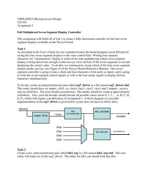
To do this, create an entity/architecture pair called seg7_driver in a file named seg7_driver.vhd.<br />
This entity should have six inputs: clk50, rst, char0, char1, char2, char3 and 2 outputs : anodes,<br />
and encodedChar. The reset should asynchronous. The anodes should be swept at approximately<br />
a kilohertz. Also, your led decoder should decode all possible values (from 0, 1, 2, …A, B, C, D,<br />
E, F), which will require a modification of <strong>Assignment</strong> 1. A block diagram of a possible<br />
implementation of the seg7_driver is given below (yours does not have to follow this):<br />
50mHz<br />
make 1kHz<br />
~1kHz<br />
char<br />
char<br />
char<br />
char<br />
calc<br />
currentAnode<br />
set_anodes<br />
led_decoder<br />
anodes<br />
encodedchar<br />
Task 2<br />
Create a new entity/architecture pair called lab2_top in a file named lab2_top.vhd. This new<br />
entity will make use of the seg7_driver. The entity for lab2_top should look like this:
entity lab2_top is<br />
port (<br />
clk50 : in std_logic;<br />
BTN1 : in std_logic;<br />
sliderSwitches : in std_logic_vector(3 downto 0);<br />
Seg7 : out std_logic_vector(6 downto 0);<br />
anodes : out std_logic_vector(3 downto 0) );<br />
Your top level will test your seven-segment driver as follows. BTN1 is an asynchronous reset,<br />
and when pressed, the seven-segment display will display all zeros. During normal operation, the<br />
values on the seven-segment display will be shifted left, and the value currently on the<br />
sliderSwitches(3 downto 0) will be visible on the rightmost seven-segment display. So, as you<br />
change the values on the switches you will see the characters slowly “scroll” left.<br />
A small block diagram of how this might be implemented is below (yours does not have to<br />
follow this):<br />
reset-BTN1<br />
50mHz<br />
make 1hz<br />
load&shift<br />
enable<br />
switches(3:0)<br />
current<br />
chars<br />
led_driver<br />
char(3:0)<br />
anodes<br />
encodedChar<br />
Your design will need to store the four current seven-segment characters (unencoded) and will<br />
need to shift them. Therefore, the block “current chars” can be thought of as a four bit wide<br />
shift-register (4 deep) with an enable signal that is the 1Hz signal divided down from the 50MHz<br />
clock.<br />
Task 3<br />
Using the constraints editor (or a text editor) set the pin assignments for the ports of lab2_top to<br />
the appropriate Xilinx pin numbers as shown in the document. Synthesize, generate a<br />
programming file, and upload this file to the board using IMPACT. Test your design to verify<br />
that it works.
To Turn In<br />
1) Readable paper copies of appropriately commented <strong>VHDL</strong> for lab2_top.vhd and<br />
seg7_driver.vhd.<br />
2) The zipped project directory (lab2_yourlastname.zip) and the bit file<br />
(lab2_yourlastname.bit) via the submission link on the webpage. This must be turned in<br />
by 4:25 on the day of class.<br />
3) Bring your board with the assignment loaded into the non-volatile memory so that all that<br />
is required to demo the assignment is simply powering the board. An instructor will<br />
check for correct operation during the lab period
Grading Sheet<br />
20 points<br />
DEMO: 7 segment display capable of displaying 4 separate characters.<br />
20 points<br />
DEMO: Switch values shifted into display at approximately 1 Hz rate.<br />
10 points<br />
DEMO: Brief press and release of BTN1 resets display to all 0’s.<br />
15 points<br />
DEMO: PROM programmed correctly to allow power-on operation without manual<br />
configuration.<br />
35 points<br />
Quality of <strong>VHDL</strong> code and hardware design. Graded from printed copies submitted in class.