

O - DPG-Verhandlungen
O - DPG-Verhandlungen
O - DPG-Verhandlungen

You also want an ePaper? Increase the reach of your titles
YUMPU automatically turns print PDFs into web optimized ePapers that Google loves.
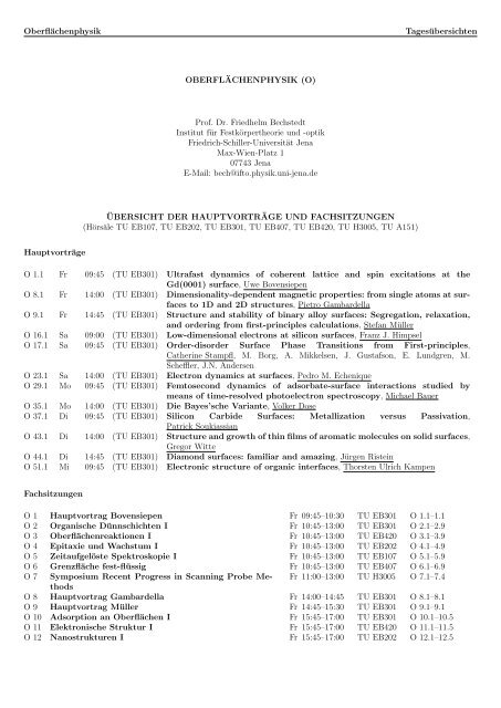
Oberflächenphysik Tagesübersichten<br />
Hauptvorträge<br />
OBERFLÄCHENPHYSIK (O)<br />
Prof. Dr. Friedhelm Bechstedt<br />
Institut für Festkörpertheorie und -optik<br />
Friedrich-Schiller-Universität Jena<br />
Max-Wien-Platz 1<br />
07743 Jena<br />
E-Mail: bech@ifto.physik.uni-jena.de<br />
ÜBERSICHT DER HAUPTVORTRÄGE UND FACHSITZUNGEN<br />
(Hörsäle TU EB107, TU EB202, TU EB301, TU EB407, TU EB420, TU H3005, TU A151)<br />
O 1.1 Fr 09:45 (TU EB301) Ultrafast dynamics of coherent lattice and spin excitations at the<br />
Gd(0001) surface, Uwe Bovensiepen<br />
O 8.1 Fr 14:00 (TU EB301) Dimensionality-dependent magnetic properties: from single atoms at surfaces<br />
to 1D and 2D structures, Pietro Gambardella<br />
O 9.1 Fr 14:45 (TU EB301) Structure and stability of binary alloy surfaces: Segregation, relaxation,<br />
and ordering from first-principles calculations, Stefan Müller<br />
O 16.1 Sa 09:00 (TU EB301) Low-dimensional electrons at silicon surfaces, Franz J. Himpsel<br />
O 17.1 Sa 09:45 (TU EB301) Order-disorder Surface Phase Transitions from First-principles,<br />
Catherine Stampfl, M. Borg, A. Mikkelsen, J. Gustafson, E. Lundgren, M.<br />
Scheffler, J.N. Andersen<br />
O 23.1 Sa 14:00 (TU EB301) Electron dynamics at surfaces, Pedro M. Echenique<br />
O 29.1 Mo 09:45 (TU EB301) Femtosecond dynamics of adsorbate-surface interactions studied by<br />
means of time-resolved photoelectron spectroscopy, Michael Bauer<br />
O 35.1 Mo 14:00 (TU EB301) Die Bayes’sche Variante, Volker Dose<br />
O 37.1 Di 09:45 (TU EB301) Silicon Carbide Surfaces: Metallization versus Passivation,<br />
Patrick Soukiassian<br />
O 43.1 Di 14:00 (TU EB301) Structure and growth of thin films of aromatic molecules on solid surfaces,<br />
Gregor Witte<br />
O 44.1 Di 14:45 (TU EB301) Diamond surfaces: familiar and amazing, Jürgen Ristein<br />
O 51.1 Mi 09:45 (TU EB301) Electronic structure of organic interfaces, Thorsten Ulrich Kampen<br />
Fachsitzungen<br />
O 1 Hauptvortrag Bovensiepen Fr 09:45–10:30 TU EB301 O 1.1–1.1<br />
O 2 Organische Dünnschichten I Fr 10:45–13:00 TU EB301 O 2.1–2.9<br />
O 3 Oberflächenreaktionen I Fr 10:45–13:00 TU EB420 O 3.1–3.9<br />
O 4 Epitaxie und Wachstum I Fr 10:45–13:00 TU EB202 O 4.1–4.9<br />
O 5 Zeitaufgelöste Spektroskopie I Fr 10:45–13:00 TU EB107 O 5.1–5.9<br />
O 6 Grenzfläche fest-flüssig Fr 10:45–13:00 TU EB407 O 6.1–6.9<br />
O 7 Symposium Recent Progress in Scanning Probe Me- Fr 11:00–13:00 TU H3005 O 7.1–7.4<br />
thods<br />
O 8 Hauptvortrag Gambardella Fr 14:00–14:45 TU EB301 O 8.1–8.1<br />
O 9 Hauptvortrag Müller Fr 14:45–15:30 TU EB301 O 9.1–9.1<br />
O 10 Adsorption an Oberflächen I Fr 15:45–17:00 TU EB301 O 10.1–10.5<br />
O 11 Elektronische Struktur I Fr 15:45–17:00 TU EB420 O 11.1–11.5<br />
O 12 Nanostrukturen I Fr 15:45–17:00 TU EB202 O 12.1–12.5
Oberflächenphysik Tagesübersichten<br />
O 13 Magnetismus Fr 15:45–17:00 TU EB107 O 13.1–13.5<br />
O 14 Struktur und Dynamik reiner Oberflächen Fr 15:45–16:45 TU EB407 O 14.1–14.4<br />
O 15 Postersitzung (Adsorption an Oberflächen, Epita- Fr 17:00–20:00 Poster TU D O 15.1–15.84<br />
O 16<br />
xie und Wachstum, Organische Dünnschichten, Oxide<br />
und Isolatoren, Rastersondentechniken, Zeitaufgelöste<br />
Spektroskopie, Methoden)<br />
Hauptvortrag Himpsel Sa 09:00–09:45 TU EB301 O 16.1–16.1<br />
O 17 Hauptvortrag Stampfl Sa 09:45–10:30 TU EB301 O 17.1–17.1<br />
O 18 Adsorption an Oberflächen II Sa 10:45–13:00 TU EB301 O 18.1–18.9<br />
O 19 Nanostrukturen II Sa 10:45–13:00 TU EB420 O 19.1–19.9<br />
O 20 Organische Dünnschichten II Sa 10:45–13:00 TU EB202 O 20.1–20.9<br />
O 21 Elektronische Struktur II Sa 10:45–13:00 TU EB107 O 21.1–21.9<br />
O 22 Rastersondentechniken I Sa 10:45–13:00 TU EB407 O 22.1–22.9<br />
O 23 Hauptvortrag Echenique Sa 14:00–14:45 TU EB301 O 23.1–23.1<br />
O 24 Teilchen und Cluster I Sa 15:00–17:00 TU EB301 O 24.1–24.8<br />
O 25 Zeitaufgelöste Spektroskopie II Sa 15:00–17:00 TU EB420 O 25.1–25.8<br />
O 26 Oxide und Isolatoren I Sa 15:00–17:00 TU EB202 O 26.1–26.8<br />
O 27 Phasenübergänge Sa 15:00–16:45 TU EB107 O 27.1–27.7<br />
O 28 Methodisches (Exp. und Theorie) Sa 15:00–17:00 TU EB407 O 28.1–28.8<br />
O 29 Hauptvortrag Bauer (Gaede-Preis) Mo 09:45–10:30 TU EB301 O 29.1–29.1<br />
O 30 Adsorption an Oberflächen III Mo 10:45–13:00 TU EB301 O 30.1–30.9<br />
O 31 Organische Dünnschichten III Mo 10:45–13:00 TU EB420 O 31.1–31.9<br />
O 32 Nanostrukturen III Mo 10:45–13:00 TU EB202 O 32.1–32.9<br />
O 33 Teilchen und Cluster II Mo 10:45–13:00 TU EB107 O 33.1–33.9<br />
O 34 Rastersondentechniken II Mo 10:45–13:00 TU EB407 O 34.1–34.9<br />
O 35 Hauptvortrag Dose (R.W. Pohl-Preis) Mo 14:00–14:45 TU EB301 O 35.1–35.1<br />
O 36 Postersitzung (Elektronische Struktur, Grenzfläche<br />
fest-flüssig, Halbleiteroberflächen und -grenzflächen,<br />
Mo 15:00–18:00 Poster TU F O 36.1–36.79<br />
Nanostrukturen, Oberflächenreaktionen, Teilchen<br />
O 37<br />
und Cluster, Struktur und Dynamik reiner Oberflächen)<br />
Hauptvortrag Soukiassian Di 09:45–10:30 TU EB301 O 37.1–37.1<br />
O 38 Halbleiteroberflächen und -grenzflächen Di 10:45–13:00 TU EB301 O 38.1–38.9<br />
O 39 Nanostrukturen IV Di 10:45–13:00 TU EB420 O 39.1–39.9<br />
O 40 Adsorption an Oberflächen IV Di 10:45–13:00 TU EB202 O 40.1–40.9<br />
O 41 Elektronische Struktur III Di 10:45–13:00 TU EB107 O 41.1–41.9<br />
O 42 Oberflächenreaktionen II Di 10:45–13:00 TU EB407 O 42.1–42.9<br />
O 43 Hauptvortrag Witte Di 14:00–14:45 TU EB301 O 43.1–43.1<br />
O 44 Hauptvortrag Ristein Di 14:45–15:30 TU EB301 O 44.1–44.1<br />
O 45 Organische Dünnschichten IV Di 15:45–18:30 TU EB301 O 45.1–45.11<br />
O 46 Adsorption an Oberflächen V Di 15:45–18:30 TU EB420 O 46.1–46.11<br />
O 47 Rastersondentechniken III Di 15:45–18:30 TU EB202 O 47.1–47.11<br />
O 48 Oxide und Isolatoren II Di 15:45–18:30 TU EB107 O 48.1–48.11<br />
O 49 Epitaxie und Wachstum II Di 15:45–18:30 TU EB407 O 49.1–49.11<br />
O 50 Postdeadline-Session Di 20:00–21:00 TU A151 O 50.1–50.4<br />
O 51 Hauptvortrag Kampen Mi 09:45–10:30 TU EB301 O 51.1–51.1<br />
O 52 Elektronische Struktur IV Mi 10:45–13:00 TU EB301 O 52.1–52.9<br />
O 53 Organische Dünnschichten V Mi 10:45–13:00 TU EB420 O 53.1–53.9<br />
O 54 Adsorption an Oberflächen VI Mi 10:45–13:00 TU EB202 O 54.1–54.9<br />
O 55 Epitaxie und Oberflächenreaktionen Mi 10:45–13:00 TU EB107 O 55.1–55.9<br />
Mitgliederversammlung des Fachverbands Oberflächenphysik<br />
Di 19:30–20:00 A151 (Architekturgebäude)<br />
Vorläufige Tagesordnung:<br />
- Bericht des Fachverbandsvorsitzenden<br />
- Verschiedenes
Oberflächenphysik Tagesübersichten<br />
HINWEISE:<br />
Postersitzung O7 am Freitag (17:00-20:00) im Bereich TU D (HG 3. OG)<br />
Die Poster können ab Freitagmorgen aufgehängt werden und sollen nach der Postersitzung entfernt werden.<br />
Der Abend wird unterstützt von Omicron Vakuumphysik GmbH.<br />
Postersitzung O36 am Montag (15:00-18:00) im Bereich TU F (PN unten)<br />
Die Poster können ab Montag 8:00 Uhr aufgehängt werden und sollten nach der Postersitzung entfernt werden.<br />
Postdeadlinesitzung O50 am Dienstag von 20:00-21:00 Uhr im Hörsaal TU A151 (Architekturgebäude), von<br />
21:00-23:30 Uhr im Foyer des Architekturgebäudes<br />
Deadline für die Einladung ist der 15. Februar 2004.<br />
Die Sitzung wird unterstützt von SPECS GmbH zusammen mit BESTEC GmbH, VTS CREATEC GmbH und<br />
Oxford Scientific Ltd.<br />
GEMEINSAME VERANSTALTUNGEN UND SYMPOSIEN MIT ANDEREN FACHVERBÄNDEN:<br />
O7 Symposium Recent Progress in Scanning Probe Methods<br />
Freitag, 04.03.2005, 10:15-13:00 Uhr, Hörsaal TU HE101 (1. Vortrag Rugar, gemeinsam mit SYQL)<br />
Fortsetzung 11:00 Uhr, Hörsaal TU H3005<br />
DS21 Symposium Optical Spectroscopy of Thin Films and Interfaces<br />
Dienstag, 08.03.2005, 09:45-13:30 und 14:30-16:45 Uhr, Hörsaal TU H110<br />
SYSR Symposium Highlights in Synchrotron Radiation Research<br />
Samstag, 05.03.2005, 08:30-13:00 Uhr, Hörsaal TU HE101<br />
SYOO Symposium Optoelectronics and Photonics<br />
Montag, 07.03.2005, 14:00 Uhr, Hörsaal TU HE101
Oberflächenphysik Freitag<br />
Fachsitzungen<br />
– Haupt-, Fach-, Kurzvorträge und Posterbeiträge –<br />
O 1 Hauptvortrag Bovensiepen<br />
Zeit: Freitag 09:45–10:30 Raum: TU EB301<br />
Hauptvortrag O 1.1 Fr 09:45 TU EB301<br />
Ultrafast dynamics of coherent lattice and spin excitations at<br />
the Gd(0001) surface — •Uwe Bovensiepen — Freie Universität<br />
Berlin, Fachbereich Physik, Arnimallee 14, 14195 Berlin<br />
The dynamics of collective excitations of electrons, spins and phonons<br />
are of fundamental interest to develop a microscopic understanding of elementary<br />
interactions and relaxation mechanisms of these quasiparticles.<br />
Based on magnetoelasticity, magnon-phonon interaction is usually attributed<br />
to spin-orbit coupling which transfers a displacement of ion cores<br />
in the lattice to the spin system and vice versa. However, a microscopic<br />
picture is generally not available. Here, ferromagnetic Gd(0001) characterized<br />
by a very weak spin-orbit coupling and its exchange-split d z 2-surface<br />
state serves as a model system for such coupled phonon-magnon modes,<br />
O 2 Organische Dünnschichten I<br />
which can be excited coherently by femtosecond laser pulses. Gd(0001)<br />
is investigated by complimentary pump-probe-experiments of non-linear<br />
optical second harmonic generation (SHG) and time-resolved photoemission<br />
(TRPE). SHG separates electron/lattice and spin dynamics by their<br />
symmetry with respect to magnetization reversal. A coherent phononmagnon<br />
mode at 2.9 THz is observed in the transient SHG response,<br />
which is driven by electronic excitation of surface and bulk states and is<br />
damped by scattering with electrons as well as thermalized phonons and<br />
spin waves. TRPE adds information on the interaction mechanism. We<br />
find that the binding energy of the surface state oscillates at 3 THz as<br />
well, which suggests a parametric phonon-magnon-coupling by modulation<br />
of the exchange splitting, contrary to the conventional type mediated<br />
by spin-orbit-interaction.<br />
Zeit: Freitag 10:45–13:00 Raum: TU EB301<br />
O 2.1 Fr 10:45 TU EB301<br />
Investigating the stability of the tetracene/Al2O3-interface with<br />
high-resolution electron energy loss spectroscopy and LEED —<br />
•R. Temirov 1 , A. Langner 2 , M. Sokolowski 2 , and F.S. Tautz 1<br />
— 1 International University Bremen, School of Engineering and Science,<br />
PO Box 750761, D-28725 Bremen — 2 Institut für Physikalische und<br />
Theoretische Chemie, Universität Bonn, Wegelerstr. 12, D-53115 Bonn<br />
Surprisingly, fluorescence of tetracene molecules in contact with a sapphire<br />
substrate is quenched, in spite of the fact that the high band gap<br />
of Al2O3 should provide an effective barrier to charge delocalisation [1].<br />
The reappearance of luminescence after annealing thin tetracene layers<br />
to 240 K can be explained by a reduction of the tetracene/substrate<br />
interaction, either by molecular reorientation or dewetting of the interface.<br />
Here we report an HREELS investigation of the interface between<br />
thin epitaxial Al2O3-layers on Ni3Al(111) and tetracene. Our experiments<br />
show that under the current deposition conditions (thermal evaporation<br />
onto a sample at T=80K) at least some tetracene molecules are oriented<br />
with their molecular plane parallel to the substrate. The maximized contact<br />
area between molecule and substrate may be an important factor<br />
in understanding the observed luminescence quenching. Our data also<br />
suggest that after annealing, contact area is minimized by the formation<br />
of three-dimensional tetracene islands. [1] M. Schneider, E. Umbach, A.<br />
Langner, M. Sokolowski, Journal of Luminescence 110, 275-283 (2004).<br />
O 2.2 Fr 11:00 TU EB301<br />
Tripod Liganden für starre und geordnete selbstorganisierte<br />
Monolagen auf Gold — •T. Weidner 1,2 , A. Krämer 3,2 , U. Siemeling<br />
3,2 und F. Träger 1,2 — 1 Institut für Physik, Universität Kassel,<br />
Heinrich-Plett-Str. 40, 34132 Kassel — 2 Center for Interdisciplinary<br />
Nanostructure Science and Technology - CINSaT, Universität Kassel,<br />
Heinrich-Plett-Str. 40, 34132 Kassel — 3 Institut für Chemie, Universität<br />
Kassel, Heinrich-Plett-Str. 40, 34132 Kassel<br />
Selbstorganisation maßgescheiderter Moleküle auf Oberflächen ist ein<br />
verbreitetes und vielversprechendes Konzept, hoch geordnete funktionelle<br />
monomolekulare Schichten auf Edelmetalloberflächen zu präparieren.<br />
Entscheidend für Anwendungen in Katalyse, Sensorik und Datenspeicherung<br />
ist es, eine definierte und stabile Anordnung der funktionellen<br />
Einheiten zu gewährleisten.<br />
Um dieses Ziel zu erreichen, haben wir äußerst starre, tripodale<br />
Tris[(methylthio)-methyl]silyl Ankergruppen synthetisiert. Untersuchungen<br />
der Phenyl- und Biphenylderivate dieser ”dreibeinig” aufgebauten<br />
Ankergruppe auf Goldsubstraten mit Infrarotspektroskopie und Rastertunnelmikroskopie,<br />
sowie der Adsorptions- und Ordnungskinetik mit optischer<br />
Frequenzverdopplung und Ellipsometrie zeigen deutlich, dass beide<br />
Verbindungen auf Gold adsorbieren. Darüber hinaus konnte die Entstehung<br />
sehr stabiler und geordneter Phenyl- und Biphenyl-Monolagen<br />
in situ verfolgt werden.<br />
O 2.3 Fr 11:15 TU EB301<br />
Molekulare Magnete auf Oberflächen — •Miriam Klusmann,<br />
Andrea Kahlen und Marika Schleberger — Universität<br />
Duisburg-Essen, Fachbereich Physik, 45117 Essen<br />
Durch geeignete Präparationstechniken wurden die magnetischen Moleküle<br />
Ti4 und Mo72Fe30 auf die Schichtsubstrate Glimmer und HOPG<br />
aufgebracht. Untersuchungen mit den Rastersondenmethoden AFM<br />
(Atomic Force Microscopy, Rasterkraftmikroskopie) und STM (Scanning<br />
Tunneling Microscopy, Rastertunnelmikroskopie) zeigen eine Ausbildung<br />
von Ti4-Inseln auf Glimmer sowie die Selbstorganisation von Mo72Fe30<br />
auf HOPG. Da das Lösungsmittel Dichlormethan, welches zur Deponierung<br />
von Ti4 auf Glimmer verwendet wird, einen ungünstigen Einfluss<br />
auf das Substrat nimmt, ist eine qualitative Auswertung der aus AFM-<br />
Messungen gewonnenen Topographie-Daten nur unter Berücksichtigung<br />
der simultan aufgezeichneten Signale der Frequenzverschiebung und<br />
der Dämpfung der Cantilever-Oszillation möglich. Die Adsorption von<br />
Mo72Fe30 ist abhängig von der Konzentration der Moleküle in Lösung,<br />
so dass sich verschiedene Strukturen auf dem HOPG-Substrat ausbilden<br />
- von Ringen über Ketten bis hin zu Einfach- oder Mehrfachlagen.<br />
O 2.4 Fr 11:30 TU EB301<br />
Aliphatic selenolates on gold and silver substrates — •Andrey<br />
Shaporenko 1 , Avi Ulman 2 , Andreas Terfort 3 und Michael<br />
Zharnikov 1 — 1 Angewandte Physikalische Chemie, Universität<br />
Heidelberg, Im Neuenheimer Feld 253, 69120 Heidelberg, Germany —<br />
2 Department of Chemical Engineering, Polytechnic University, Brooklyn<br />
11201, New York, USA — 3 Anorganische und Angewandte Chemie,<br />
Universität Hamburg, 20146 Hamburg, Germany<br />
We studied self-assembled monolayers (SAMs) formed from didodecyl<br />
diselenide (C12SeSeC12) and didodecyl selenide (C12SeC12) on (111) Au<br />
and Ag substrates. C12SeSeC12 was found to form contamination-free,<br />
densely-packed, and well-ordered C12Se SAMs on both substrates, whereas<br />
the adsorption of C12SeC12 occurred only on Au and resulted in<br />
the formation of a SAM-like C12SeC12 film with a low packing density<br />
and a conformational disorder. The properties of the C12Se SAMs were<br />
compared with those of dodecanethiolate (C12S) SAMs. The packing<br />
density, orientational order, and molecular inclination in C12Se/Au and<br />
C12S/Au were found to be very similar. In contrast, C12Se/Ag exhibited<br />
significantly lower packing density, a lower degree of the conformational<br />
and orientational order, and a larger molecular inclination than C12S/Ag.<br />
The results suggest a sp 3 bonding configuration for the selenium atom on<br />
Au and Ag and indicate a larger corrugation of the headgroup-substrate<br />
binding energy surface in C12Se/Ag than in C12S/Ag.
Oberflächenphysik Freitag<br />
O 2.5 Fr 11:45 TU EB301<br />
Periodical density functional theory study of the bonding of aromatic<br />
organic molecules containing carboxylate group on metal<br />
surfaces — •Nicolae Atodiresei, Azadeh Farahzadi, Kurt<br />
Schroeder, and Stefan Blügel — Institut für Festkörperforschung,<br />
Forschungszentrum Jülich, D-52425 Jülich, Germany<br />
The family of five-membered heterocycles and its derivates is of basic<br />
importance in chemistry and physics. Much work is now undertaken<br />
in molecular self-assembly experiments which lead to oriented growth of<br />
organic films. We study the structure of adsorbed carboxylic acids containing<br />
furan, thiophene, selenophene and tellurophene aromatic rings in<br />
a (2x1) cell on Cu(110) surface by ab initio calculations. In the stable<br />
configuration the molecules sit perpendicular in bridge position above the<br />
first Cu-surface layer with the carboxylate group oriented along to the<br />
[1¯10] direction. In the gas phase the single molecule has a planar geometry<br />
with an extended π-system over the five-membered ring and carboxylate<br />
group. The adsorption of the molecules breaks this planarity. Due to the<br />
strong lateral interactions between the hydrogen atoms of neighboring<br />
adsorbed molecules the rings are rotated by ∼ 24 ◦ relative to the carboxylate<br />
group.<br />
O 2.6 Fr 12:00 TU EB301<br />
Growth of thin para-sexiphenyl films on Cu(110) and Cu(110)-<br />
(2x1)O — •K. Maschek, Y. Hu, L.D. Sun, M. Hohage, and<br />
P. Zeppenfeld — Institut für Experimentalphysik, Johannes-Kepler-<br />
Universität Linz, Austria<br />
Para-sexiphenyl (P6P) has attracted considerable interest as a promising<br />
candidate for future organic opto-electronic applications. Its molecular<br />
structure consists of a linear chain of six linked benzene rings showing<br />
strong π bond delocalization in the direction of the chains. Previous research<br />
shows that the optical absorption of P6P films depends strongly<br />
on the molecular orientation. On the other hand, Reflectance Difference<br />
Spectroscopy (RDS) has been demonstrated to be a powerful tool to<br />
measure the optical anisotropy at normal incidence. Here, we present a<br />
RDS investigation of para-sexiphenyl thin film growth on Cu(110) and<br />
Cu(110)-(2x1)O. The RDS spectra show a pronounced anisotropy of the<br />
P6P films formed on both substrates at room temperature, indicating<br />
preferential orientation of P6P molecules on these two atomically well<br />
defined substrates: On Cu(110), the P6P molecular chains align in the<br />
[110] direction, i.e., along the Cu atomic rows, while on the Cu(110)-<br />
(2x1)O surface, the molecules align in the orthogonal [001] direction, i.e.,<br />
along the Cu-O rows formed on Cu(110). Additionally, the evolution of<br />
the RDS signal at different photon energies during growth provides detailed<br />
information about the growth mode of P6P on both substrates.<br />
O 2.7 Fr 12:15 TU EB301<br />
Ab-initio investigation of organic molecules on metal surfaces:3nitrothiophen/selenophen/tellurophen<br />
on Cu(110) — •Azadeh<br />
Farahzadi 1,2 , Nicolae Atodiresei 1 , Stefan Blügel 1 , and Kurt<br />
Schroeder 1 — 1 Institut für Festkörperforschung, Forschungszentrum<br />
Jülich, 52425 Jülich — 2 I.Physikalisches Institut, RWTH-Aachen Sommmerfeldstraße<br />
14, 52074<br />
The future of nanoelectronics may consist in hybrid structures build of<br />
organic molecules and inorganic materials. The interesting family of fivemember<br />
heterocycles which includes thiophen/selenophen/tellurophen<br />
rings, plays an important role in constructing the charge carrier poly-<br />
O 3 Oberflächenreaktionen I<br />
mers. Based on the density functional theory (DFT) in the generalized<br />
gradient approximation (GGA), we have optimized the geometric structure<br />
of the single molecules, 3-nitrothiophen/selenophene/tellurophen<br />
and the dense-packed structure ((2 × 1) unit cell) of these molecules<br />
on the Cu(110) surface. In the stable configuration the molecules sit perpendicular<br />
to the surface with the nitro group (−NO2) along the [110]<br />
direction. In the gas phase the single molecules have a planar geometry<br />
but the adsorption of the molecules breaks this planarity. We discuss<br />
the electronic structure and the binding energy of the molecule at the<br />
surface. The calculations have been carried out using the PAW-method<br />
EStCoMPP.<br />
O 2.8 Fr 12:30 TU EB301<br />
Transfer and amplification of chirality in hydrocarbon monolayers<br />
— •Karl-Heinz Ernst, Manfred Parschau, Roman Fasel,<br />
and Sara Romer — Empa-Materials Science and Technology, 8600<br />
Duebendorf, Schweiz<br />
We present a new form of chirality transfer and amplification observed<br />
in two-dimensional monolayers. In the first case, a special surface enantiomorphism<br />
is observed via STM after adsorption of the enantiomers of<br />
a helical aromatic hydrocarbon on Cu(111) at 50 K. Instead of crystallization<br />
into homochiral domains on the surface, racemic mirror domains<br />
are observed, i.e., they possess an equimolar content of left- and righthanded<br />
molecules. In this situation, a small excess of one chiral species is<br />
sufficient to create domains of a single handedness throughout the whole<br />
surface layer. In the second case, homochirality was induced in monolayers<br />
of achiral molecules after chiral doping. Achiral molecules can become<br />
chiral when adsorbed at surfaces because of the reduced symmetry in the<br />
molecule or the adsorbate lattice. Adsorbed on Cu(110), succinic acid<br />
forms equal numbers of left- and right-handed domains and the surface<br />
is globally achiral. Doping with small amounts of left- or right-handed<br />
tartaric acid, however, creates homochirality and the opposite mirror domains<br />
are not observed anymore in the LEED pattern. Our findings are<br />
explained by cooperative interactions and will be discussed in the frame<br />
of a one-dimensional random-field Ising model.<br />
O 2.9 Fr 12:45 TU EB301<br />
STM investigations of ordered monolayers of tetralactam<br />
macrocycles on Au(111) — •Iordan Kossev and Moritz<br />
Sokolowski — Institut für Physikalische und Theoretische Chemie,<br />
Universität Bonn, Wegelerstr. 12, 53115 Bonn, Germany<br />
Rotaxanes and catenanes are of interest for the investigation on mechanically<br />
interlocked molecules [1]. A large tetralactam - macrocycle<br />
(905.05 amu), very often used as a building block for catenanes, was deposited<br />
onto the Au(111) surface in UHV from a thermal evaporation<br />
cell. STM images were taken for different coverages at room temperature.<br />
At a coverage around one monolayer, different long range ordered<br />
monolayer structures were observed with submolecular resolution on the<br />
terraces. After annealing to 400 K, in addition to the two dimensional<br />
structures, chains of well ordered molecules adsorbed at step edges were<br />
observed. We explain these STM images by structure models based on a<br />
weak interaction of the molecules to the Au(111) surface and a considerable<br />
intermolecular interaction due to hydrogen bonds. The macrocycles<br />
were kindly supplied by C. Schalley and F. Vögtle. This work was supported<br />
by the DFG (SFB 624).<br />
[1] C. A. Schalley, K. Beizai, F. Vögtle, Acc. Chem. Res. 34 (2001) 465.<br />
Zeit: Freitag 10:45–13:00 Raum: TU EB420<br />
O 3.1 Fr 10:45 TU EB420<br />
Investigation of Au/TiO2 model catalysts prepared from micellar<br />
stabilized gold particles — •S. Kielbassa 1 , F. Weigl 2 , A.<br />
Ethirajan 2 , H.G. Boyen 2 , P. Ziemann 2 und R.J. Behm 1 — 1 Abt.<br />
Oberflächenchemie und Katalyse, Universität Ulm, 89069 Ulm — 2 Abt.<br />
Festkörperphysik, Universität Ulm, 89069 Ulm<br />
Metal oxide supported Au catalysts have attracted considerable interest<br />
over the last years because of their high activity for low-temperature<br />
oxidation and hydrogenation reactions. For studying particle size and<br />
transport effects, we prepared model systems with a narrow distribution<br />
for particle sizes and particle separations by depositing Au loaded diblock<br />
copolymer micelles onto atomically smooth TiO2 (110) rutile substrates.<br />
Removing of the polymer shells in an oxygen plasma leads to a hexagonal<br />
arrangement of Au particles. The stability of these model systems<br />
in typical activation and reaction atmospheres/temperatures as well as<br />
their activity for CO oxidation under high pressure conditions was investigated<br />
for different particle sizes and seperations. Consequences on the<br />
reaction mechanism are discussed.<br />
O 3.2 Fr 11:00 TU EB420<br />
Catalytic properties of UHV-prepared Au/TiO2-model systems<br />
at elevated pressures up to 100 mbar — •Thomas Diemant,<br />
Zhong Zhao, Hubert Rauscher, and R. J. Behm — Abt.<br />
Oberfächenchemie und Katalyse, Universität Ulm, 89069 Ulm
Oberflächenphysik Freitag<br />
Oxide supported Au catalysts have found increasing interest because<br />
of their high activity for various oxidation and reduction reactions. For<br />
model studies under realistic reaction conditions we performed in-situ<br />
IR spectrocopy (PEM-IRAS) and rate measurements for CO oxidation<br />
on structurally (STM) [1] and chemically (XPS, CO-TPD) well-defined<br />
model catalysts, prepared by Au deposition on thin TiO2 films at pressures<br />
up to 100 mbar. Results for various Au particle sizes, temperatures,<br />
and partial pressures are presented and discussed in comparison with data<br />
obtained on real catalysts. Consequences for the reaction mechanism are<br />
derived.<br />
[1] Zhong Zhao et al., <strong>DPG</strong>-Frühjahrstagung AKF Oberflächenphysik,<br />
Berlin (2005)<br />
O 3.3 Fr 11:15 TU EB420<br />
Reduction of the Surface Oxide Layer on Rh(111) by CO and<br />
H2 — •Jan Klikovits 1 , Michael Schmid 1 , Edvin Lundgren 2 ,<br />
Jasper N. Andersen 2 , Lukas Köhler 3 , Georg Kresse 3 , and Peter<br />
Varga 1 — 1 Institut für Allgemeine Physik, TU Wien, A-1040 Wien,<br />
Austria — 2 Department of Synchrotron Radiation Research, Lund University,<br />
Box 118, S-221 00, Sweden — 3 Inst. f. Materialphysik, Universität<br />
Wien, A-1090 Wien, Austria<br />
We have studied the surface oxide on Rh(111) and its reduction by CO<br />
and H2. The structure of the surface oxide has already been solved [1].<br />
Reducing the oxide by CO requires temperatures of about 100 ◦ C. Essentially<br />
all CO adsorbs at reduced areas, thus the reduction rate increases<br />
while the amount of oxide decreases at the surface. STM images show<br />
that the reduction starts at step edges and islands. A (2 x 2) superstructure<br />
is observed in the reduced areas. We argue that the CO molecules<br />
are immobilized by a oxygen superstructure which is in thermodynamic<br />
equilibrium with the oxide. The reduction of the surface oxide by H2 was<br />
observed in-situ by STM. It starts already at room temperature, almost<br />
exclusively in stepped areas. We can also initiate the reduction process<br />
by deliberately creating defects with the STM tip allowing us to examine<br />
the reduction kinetics in detail. At low H2 pressures or small reduced<br />
areas the reduction rate is limited by the hydrogen adsorption on the<br />
reduced area. For large reduced areas the reduction rate is limited by the<br />
processes at the border of the reduced area.<br />
[1]: J. Gustafson et al., Phys. Rev. Lett 92, 126102, (2004).<br />
O 3.4 Fr 11:30 TU EB420<br />
Hydrogen Transfer Reaction on the Surface of an Oxide catalyst<br />
— •Daniela Crihan, Marcus Knapp, and Herbert Over —<br />
Phys.Chem.Institut, Justus Liebig Univ. Giessen, D-35392 Giessen<br />
RuO 2 (110) exposes two kinds of active surface species (acidic and basic<br />
centers) which govern the interaction of the gas phase in contact with<br />
the catalysts surface. Here we will elucidate the cooperative interplay<br />
of these two active surface sites for a simple model reaction, namely<br />
the water formation over RuO 2 (110) catalysts when supplying hydrogen<br />
and oxygen from the gas phase. The bridging O atoms harvest the<br />
hydrogen from the gas phase, while the on-top O atoms picks up those<br />
adsorbed hydrogen atoms from the bridging O atoms to form water. This<br />
mechanism of hydrogen transfer is mediated by a strong hydrogen bond.<br />
Hydrogen transfer is expected to play a vital role for the whole class of<br />
catalyzed hydrogenation and dehydrogenation reactions of hydrocarbons<br />
over RuO 2 (110).<br />
O 3.5 Fr 11:45 TU EB420<br />
Interaction of Hydrogen with RuO2(110) Surfaces — •Yuemin<br />
Wang 1,2 , Jinhai Wang 2 , Chaoyang Fan 2 , Karl Jacobi 2 , and Gerhard<br />
Ertl 2 — 1 Lehrstuhl für Physikalische Chemie I, Ruhr-Universität<br />
Bochum — 2 Fritz-Haber-Institut der Max-Planck-Gesellschaft, Berlin<br />
The adsorption and reaction of hydrogen on the stoichiometric and<br />
oxygen-rich RuO2(110) surfaces - the latter exposing a weakly bound<br />
atomic oxygen species (O-cus) on-top of the unsaturated Ru atom (Rucus)<br />
- was studied using high-resolution electron energy-loss spectroscopy<br />
(HREELS) and thermal desorption spectroscopy (TDS). On the stoichiometric<br />
RuO2(110) surface two hydrogen adsorption states are identified<br />
at 85 K [1]: Molecular hydrogen at Ru-cus and dissociated hydrogen<br />
forming a dihydride with O-bridge, the other unsaturated surface oxygen<br />
besides O-cus. The dihydride is transformed into monohydride by release<br />
of hydrogen at 350 K. On oxygen-rich RuO2(110) surfaces hydrogen reacts<br />
with O-cus forming H2O-cus. This species undergoes desorption instead<br />
of dissociation with heating to higher temperatures. The reaction<br />
mechanisms of hydrogen with O-bridge and O-cus are derived.<br />
[1] Wang, J.; Fan, C. Y.; Sun, Q.; Reuter, K.; Jacobi, K.; Scheffler, M.;<br />
Ertl, G. Angew. Chem. Internat. Edition 2003, 42, 2151.<br />
O 3.6 Fr 12:00 TU EB420<br />
Interaction of supported Pd nanoparticles with H, O and C —<br />
•Günther Rupprechter, Matthias Morkel, Marta Borasio,<br />
and Hans-Joachim Freund — Fritz-Haber-Institut, Faradayweg 4-6,<br />
14195 Berlin<br />
Vibrational sum frequency generation (SFG) spectroscopy, thermal<br />
desorption spectroscopy (TDS) and photoelectron spectroscopy (XPS)<br />
were utilized to examine the interaction of Al2O3 supported Pd nanoparticles<br />
with hydrogen, oxygen and methanol. Experiments were performed<br />
both under ultrahigh vacuum (UHV) as well as mbar pressure. The Pd<br />
nanoparticles had a mean size of 5 nm and exhibited mostly (111) facets.<br />
Pd-hydride formation was observed to proceed predominantly via minority<br />
sites on Pd nanoparticles, i.e. defects and (100) faces. Explosive<br />
hydrogen desorption through a CO overlayer originates from the confinement<br />
of dissolved hydrogen within the limited nanoparticle volume. The<br />
oxidation of Pd nanoparticles under UHV and mbar pressure also seems<br />
to be strongly influenced by defects. Carbonaceous deposits that appear<br />
during methanol decomposition and oxidation are located both in surface<br />
and subsurface positions. A possible involvement of CHx species in the<br />
oxidation reaction is discussed.<br />
O 3.7 Fr 12:15 TU EB420<br />
Surface Diffusion and Fluctuations on Catalyst Nanoparticles<br />
— •Mathias Laurin 1 , Viktor Johánek 1 , Ann W. Grant 2 ,<br />
Bengt Kasemo 2 , Jörg Libuda 1 , and Hans-Joachim Freund 1 —<br />
1 Fritz-Haber-Institut der Max-Planck-Gesellschaft, Faradayweg 4–6,<br />
14195 Berlin, Germany — 2 Department of Applied Physics, Chalmers<br />
University of Technology, 41296, Göteborg, Sweden<br />
The CO oxidation and oxygen diffusion kinetics are investigated using<br />
molecular beam methods under ultrahigh vacuum (UHV). We employ<br />
oxide supported Pd nanoparticles prepared by physical vapor deposition<br />
(PVD) and electron beam lithography (EBL) covering a large range of<br />
particle sizes (1–500 nm).<br />
The angular resolved distribution of CO2 depends on the reaction conditions<br />
and particle size. In combination with the experiments, microkinetic<br />
simulations give information on the mobility of the adsorbed species<br />
under reaction conditions and on the local reaction rates on the particle<br />
surface.<br />
A macroscopic bistability of the reaction is observed at low temperatures<br />
on the big particles. It is however quenched on small nanoparticles.<br />
This is attributed to fluctuation induced transitions, accelerated in the<br />
presence of defect sites.<br />
O 3.8 Fr 12:30 TU EB420<br />
In-situ high resolution XPS study of the CO oxidation on<br />
Pt(355) — •Barbara Tränkenschuh, Thomas Fuhrmann,<br />
Christian Papp, Daniel Kiessling, Reinhard Denecke, and<br />
Hans-Peter Steinrück — Lehrstuhl für Physikalische Chemie II,<br />
Universität Erlangen-Nürnberg, Egerlandstr. 3, 91058 Erlangen<br />
The oxidation of CO on the stepped Pt(355)=[5(111)x(111)] surface<br />
was studied by in-situ high resolution XPS experiments at BESSY II. The<br />
different species and adsorption sites (O, CO on-top/bridge) on steps and<br />
terraces are clearly distinguishable in O 1s or C 1s spectra. In the experiments<br />
first an oxygen layer was prepared using a procedure, which leads<br />
to a p(2x2)-O-LEED pattern on Pt(111). On Pt(355), however, no ordered<br />
adsorbate structure was observed. Therefore, the coverages of the<br />
reactants (O, CO) were estimated by comparing the XPS intensities with<br />
those observed on Pt(111) [1]. CO was dosed by a supersonic molecular<br />
beam, which allows to vary the CO pressure on the sample. The oxidation<br />
was studied as a function of reaction temperature and CO pressure<br />
on the sample by recording time-dependent O 1s and C 1s intensities.<br />
Measurable reaction rates on Pt(355) are observed at much lower temperatures<br />
than on Pt(111) (200 vs. 270 K, respectively) [1]. The reaction<br />
product CO2 was additionally detected by mass spectrometry. Supported<br />
by the DFG (STE 620/4-2).<br />
[1] M. Kinne et al., J.Chem. Phys. 120 (2004) 7113.
Oberflächenphysik Freitag<br />
O 3.9 Fr 12:45 TU EB420<br />
Messungen an einer YSZ/Pt-Gasreferenzzelle zur elektrochemischen<br />
Promotion katalytischer Reaktionen — •Tobias Neubrand<br />
1 , Sebastian Günther 2 und Ronald Imbihl 1 — 1 Institut für<br />
Physikalische Chemie und Elektrochemie, Universität Hannover, Callinstraße<br />
3-3a, 30167 Hannover — 2 LMU München, Department Chemie,<br />
Butenandstr.11 E, 81377 München<br />
Während elektrochemischen Pumpens ändert sich bei Festelektrolyt/<br />
Metall-Systemen die Austrittsarbeit des Metalls. Es wurde eine 1:1 Beziehung<br />
zwischen Austrittsarbeitsänderung und eingestellter Spannung<br />
postuliert, die aber nur teilweise durch Messergebnisse bestätigt werden<br />
konnte. Zur Klärung dieser Frage wurde eine gasdichte elektroche-<br />
O 4 Epitaxie und Wachstum I<br />
mische Zelle für den Einsatz im UHV aufgebaut, bei der auf einem YSZ-<br />
Festkörperelektrolyten die Elektroden durch Aufsintern einer Pt-Paste<br />
aufgebracht wurden. Ein fester Sauerstoff-Referenzdruck verhindert das<br />
Verschieben des Referenzpotentials durch Anreduktion von YSZ. An dieser<br />
Zelle konnten Ratenmessungen der katalytischen CO-Oxidation an<br />
Pt mit Messungen der Austrittsarbeit korreliert werden, die integral über<br />
eine Kelvin-Sonde und lokal über Photoelektronenemissionsmikroskopie<br />
(PEEM) bestimmt wurden. Die verschiedenen Beiträge zu Kelvinsondenmessungen<br />
der Austrittsarbeit konnten damit identifiziert werden:<br />
Ein elektrostatischer durch Aufladung der Elektroden und ein ëchter”,<br />
der durch SSpillover”von O-Ionen von YSZ zur Pt-Oberfläche zustande<br />
kommt.<br />
Zeit: Freitag 10:45–13:00 Raum: TU EB202<br />
O 4.1 Fr 10:45 TU EB202<br />
Unidirectional patterning of transition-metal films on Ir(100) —<br />
•Chiara Giovanardi, Andreas Klein, Andreas Schmidt, Lutz<br />
Hammer, and Klaus Heinz — Lehrstuhl für Festkörperphysik, Universität<br />
Erlangen Nürnberg, Staudtstr. 7, D-91058 Erlangen<br />
We report and compare the unidirectional patterning of Fe, Ni and Co<br />
ultrathin films deposited on the hydrogen-stabilized substrate Ir(100)-<br />
(5×1)-H. This template develops by exposure of the Ir(100)-(5×1)-hex<br />
phase to hydrogen and consists of long, regularly spaced and defect-free<br />
Ir monoatomic wires residing on the (1×1) structured Ir substrate. The<br />
space between the wires can be filled by deposition of the transition<br />
metals (TM) Fe, Co and Ni. We show by STM that this filling process is<br />
rather different for the three metals but eventually results, at 0.8 ML coverage,<br />
in lateral superlattices {TM4Ir}. The crystallographic structure of<br />
the three compounds was determined by quantitative LEED, which also<br />
reveals that there is no intermixing of TM atoms with the Ir wires. By<br />
further TM deposition, the superlattice is covered by pure TM in a layerby-layer<br />
growth mode. In the second and third layer, atoms deviate from<br />
the ideal quadratic arrangement as induced by the 1-dim. corrugated<br />
structure of the {TM4Ir} interface. The vertical buckling of the interface<br />
is imprinted in the TM film, with a maximum amplitude of e.g. 0.11<br />
˚A in the third Ni layer. Laterally, the atomic rows above the Ir chains<br />
of the interface have a larger separation and, under special conditions,<br />
can be decorated by further TM adatoms leading to well separated chain<br />
structures on top of the film.<br />
O 4.2 Fr 11:00 TU EB202<br />
Strain relaxation in ultrathin Ni films grown on Ir(100)-(1x1)<br />
and Ir(100)-(5x1)-H — •Andreas Klein, Bernd Gumler, Lutz<br />
Hammer, and Klaus Heinz — Lehrstuhl für Festkörperphysik , Universität<br />
Erlangen-Nürnberg, Staudtstr. 7, D-91058 Erlangen<br />
We report on the growth of Ni films both on the metastable (1x1) phase<br />
and on the hydrogen-induced (5x1)-H phase of the Ir(100) surface in the<br />
coverage regime 4-10 monolayers (ML) applying STM and LEED. Whilst<br />
the (1x1) phase corresponds to the bulk-like truncated crystal, the (5x1)-<br />
H phase consists of long Ir wires of single atomic width which reside on<br />
this (1x1) phase in (on average) 5-fold lateral periodicity. On both templates<br />
an almost perfect layer-by-layer growth in the low coverage regime<br />
is followed by strain-relief controlled growth above 4 ML coverage. In<br />
this regime islands of 5 atoms width grow only one-dimensionally and<br />
eventually form irregular grids on the surface. Only with the completion<br />
of a layer the spaces within the grids are filled so that flat and homogeneous,<br />
but strained layers are formed. With film thicknesses in the range<br />
6-8 ML the layerwise growth becomes less perfect and, at about 10 ML,<br />
dislocations are formed. For the (1x1) substrate the structures mentioned<br />
extend in both the [011] and [01-1] directions, whereas on the (5x1)-H<br />
phase the Ir wires at the film-substrate interface impose their unidirectionality<br />
on the higher coverage films. Only above a coverage of about<br />
10 ML this differences between the two phases disappear and the nickel<br />
films exhibit similar patterns of strain relief.<br />
O 4.3 Fr 11:15 TU EB202<br />
Morphology and structure of pseudomorphic Ni-films grown on<br />
the Ir(100)-(1x1) surface — •Bernd Gumler, Andreas Schmidt,<br />
Andreas Klein, Lutz Hammer und Klaus Heinz — Lehrstuhl<br />
für Festkörperphysik, Universität Erlangen - Nürnberg, Staudtstr. 7, D-<br />
91058 Erlangen<br />
Recent investigations of the epitaxial growth of Ni on the hexagonally<br />
reconstructed (100) surface of iridium, Ir(100)-(5x1)-hex, have shown<br />
that the reconstruction is lifted at very low Ni coverage leading to strong<br />
intermixing at the interface resulting in a rather limited order of the film.<br />
Therefore we used the surface’s 1x1-structure, which can be prepared as<br />
metastable phase, as a template instead of the reconstructed phase. Scanning<br />
tunnelling microscopy (STM) and (quantitative) low-energy electron<br />
diffraction (LEED) were applied in the investigation. The Ni-Ir epitaxial<br />
misfit is as large as 8.2% so that layer-by-layer growth should not be<br />
expected. Indeed, we did not succeed to prepare a perfectly flat and closed<br />
2 monolayers film. Surprisingly, yet, deposition of a third Ni layer<br />
yielded an almost ideal 3 layers film, i.e. the system seems to return to<br />
layer-by-layer growth. In fact, also the 4th layer grows accordingly. The<br />
films structures were determined and verified by excellent LEED theoryexperiment<br />
fits. Structures were found to be tetragonally distorted with<br />
layer spacings of about 1.55 ˚A which are very close to the prediction of<br />
elastic theory. The structural influence of hydrogen adsorption on the<br />
films was investigated, too.<br />
O 4.4 Fr 11:30 TU EB202<br />
Nucleation in the presence of adatom insertion: Co / Pt(111)<br />
— •Philipp Buluschek, Stefano Rusponi, Mehdi El Ouali, Emmanuel<br />
Vargoz, Klaus Kern, and Harald Brune — Institute of<br />
the Physics of Nanostructures, Ecole Polytechnique Fédérale de Lausanne,<br />
CH-1015 Lausanne, Switzerland<br />
We used variable temperature STM to study submonolayer nucleation<br />
of Co / Pt(111). Our experiments show that insertion of Co adatoms into<br />
the topmost layer of the Pt surface sets in at temperatures as low as<br />
180 K. By relieving the tensile stress of the Pt surface, insertion leads to<br />
the formation of double partial dislocation lines. These take the shape of<br />
three branched stars.<br />
With the insertion and the associated reconstruction, the Co / Pt(111)<br />
system makes a transition from homogeneous to heterogeneous nucleation.<br />
The behavior of the island density as a function of deposition temperature<br />
has been modeled in kinetic Monte-Carlo simulations. We show<br />
that the partial dislocations act as repulsive line defects with a diffusion<br />
energy barrier Ed > 670 meV. The comparison between simulations and<br />
experiment also enables access to the energy barriers for surface diffusion<br />
and the density of included adatoms in the surface.<br />
O 4.5 Fr 11:45 TU EB202<br />
Growth of Copper on Nickel (111) - a Scanning Tunneling<br />
Microscopy Study — •Florian Maier, Reinhard Lindner, and<br />
Hans-Peter Steinrück — Lehrstuhl Physikalische Chemie II, Universität<br />
Erlangen-Nürnberg, Egerlandstr. 3, D-91058 Erlangen<br />
Controlled growth of bimetallic structures on a nanometer scale is of<br />
crucial interest in many fields. Therefore, the initial growth stage of copper<br />
on Ni(111) (0.05 ML < θCu < 1.5 ML) as a model system was studied<br />
with scanning tunneling microscopy (STM). Copper was deposited using<br />
an electron beam evaporator that produced a flux of neutral atoms accompanied<br />
by a small fraction of ions. The latter was controlled by a<br />
countervoltage. The island size distribution was investigated as a function<br />
of substrate temperature (100 K or room temperature), concomitant<br />
copper ions, preadsorbed layers of water, and preadsorbed carbon monoxide.<br />
In summary, room temperature promotes two-dimensional growth (due<br />
to kinetic effects), ion assisted deposition yields small islands (due to en-
Oberflächenphysik Freitag<br />
hanced nucleation center formation), deposition on preadsorbed water<br />
layers results in a morphologie analogous to Stranski-Krastanov growth<br />
(due to ”soft landing” of preformed copper clusters), and CO coadsorbtion<br />
prohibits island fusion (due to reduced diffusion length and/or step<br />
stabilisation).<br />
O 4.6 Fr 12:00 TU EB202<br />
Electronic structure of Zn on Pd(111) during growth and alloying<br />
— •Andreas Bayer, Ken Flechtner, Dieter Borgmann,<br />
Reinhard Denecke, and Hans-Peter Steinrück — Lehrstuhl für<br />
Physikalische Chemie II, Universität Erlangen-Nürnberg, Egerlandstr. 3,<br />
D-91058 Erlangen<br />
Hydrogen as energy carrier can be produced by steam reforming of<br />
methanol over Pd/ZnO catalysts. The high activity and selectivity of the<br />
catalysts is attributed to the in-situ formation of Pd-Zn alloys as one of<br />
the active components [1]. Therefore, we investigated the growth of thin<br />
Zn layers (0-3 ML) on Pd(111) at 105 K and the changes in electronic<br />
structure during subsequent annealing to higher temperatures (up to<br />
1000 K) by high-resolution X-ray photoelectron spectroscopy (XPS) with<br />
monochromized Al Kα radiation, ultraviolet photoelectron spectroscopy<br />
(UPS), and low energy electron diffraction (LEED). The formation of<br />
Pd-Zn alloys above 300 K can clearly be seen in XP spectra, as new Zn<br />
2p3/2 and Pd 3d5/2 peaks evolve. The temperatures, at which these alloys<br />
form, strongly depend on the amount of adsorbed Zn. An ordered<br />
alloy was only observed for annealing 1 ML of Zn to 400-600 K. UPS<br />
measurements show a reduction in the density of states near the Fermi<br />
edge during alloying, explaining the Cu-like catalytic behaviour.<br />
Supported by the DFG (Schwerpunktsprogramm 1091, Ste620/3-3).<br />
[1] N. Iwasa, S. Masuda, N. Ogawa, and N. Takezawa, Appl. Catal. A<br />
125 (1995) 145<br />
O 4.7 Fr 12:15 TU EB202<br />
Temperature dependent evolution of Au/Pd(110) structure —<br />
•Marko Kralj 1 , Stefan Degen 1 , Aleksander Krupski 1 , Conrad<br />
Becker 1 , Klaus Wandelt 1 , Aude Bailly 2 , Marie-Claire<br />
Saint-Lager 2 , Pierre Dolle 2 , and Robert Baudoing-Savois 2 —<br />
1 Institut für Physikalische Chemie, Bonn, Germany — 2 Laboratoire de<br />
Cristallographie, Grenoble, France<br />
Ultra thin gold films on Pd(110) are studied by surface x-ray diffraction<br />
(SXRD) and scanning tunneling microscopy (STM). The focus is set to a<br />
2.5 atomic layers thick gold film. The evolution of the room temperature<br />
deposited film structure and morphology is investigated as a function of<br />
annealing temperature in the range of 300-580 K. With increasing temperature<br />
the film order increases and the surface plane exhibits a (1 × 2)<br />
missing row reconstruction. Also, after 500 K, a competitive process of<br />
alloying with the palladium substrate takes place. A diffuse component is<br />
observed when performing transverse SXRD scans along the (01L) crystal<br />
truncation rod. This diffuse intensity is present only in one direction and<br />
is thus induced by ”defects” of anisotropic form. We propose a consistent<br />
model which clearly relates this effect to the STM data.<br />
O 5 Zeitaufgelöste Spektroskopie I<br />
O 4.8 Fr 12:30 TU EB202<br />
Bcc-like crystal structures in ultrathin ”fcc”Fe films on Cu(111)<br />
— •Albert Biedermann, Werner Rupp, Michael Schmid, and<br />
Peter Varga — Institut für Allgemeine Physik, Vienna University of<br />
Technology, 1040 Vienna, Austria<br />
Growing ultrathin Fe films on fcc substrates can stabilize the fcc structure<br />
of Fe. More often, however, distorted bcc-like structures are found<br />
instead. Fe/Cu(100) films are very flat and show relatively well defined<br />
fcc and bcc-like phases, among them a ”nanomartensitic”bcc-like phase<br />
[1]. In contrast, Fe/Cu(111) films grown by thermal deposition are relatively<br />
rough, favoring Cu surface segregation and hampering standard<br />
LEED-I/V analyses. We have used atomically resolved STM and STS of<br />
clean and H-covered bi- and multi-layer islands together with XPD data<br />
by Kief and Egelhoff [2] to show the presence and conditions of stability<br />
of strained bcc-like phases in Fe/Cu(111) films. Our results are compared<br />
to published magnetic measurements [3] and first principles predictions<br />
[4], which favor an ideal fcc phase for very thin films.<br />
[1] A. Biedermann, R. Tscheließnig, M. Schmid, and P. Varga, Appl.<br />
Phys. A 78 (2004) 807.<br />
[2] M. T. Kief, W. F. Egelhoff, Jr, Phys. Rev. B 47 (1993) 10785<br />
[3] P. Ohresser, J. Shen, J. Barthel, M. Zheng, C. V. Mohan, M. Klaua,<br />
and J. Kirschner, Phys. Rev. B 59, 3696 (1999).<br />
[4] Spiˇsák and J. Hafner, PRB 67 (2003) 134434<br />
O 4.9 Fr 12:45 TU EB202<br />
Growth and electronic structure of ultrathin chromium films<br />
on iridium(111) investigated by scanning tunneling microscopy<br />
and spectroscopy — •Felix Marczinowski, Kirsten von<br />
Bergmann, and Roland Wiesendanger — Institut für Angewandte<br />
Physik, Universität Hamburg<br />
Magnetic materials are showing interesting properties when prepared<br />
as thin films. Bulk Cr has bcc structure and is antiferromagnetic. Instead,<br />
if grown as a hexagonal monolayer film, the antiferromagnetic<br />
alignment of neighbouring atomic moments is impossible and a frustrated<br />
spin-structure will be formed [D. Wortmann et al., Resolving Complex<br />
Atomic-Scale Spin Structures by Spin-Polarized Scanning Tunneling Microscopy,<br />
PRL(2001)]. To study this spin-structure on an atomic level,<br />
Cr films of various coverages were deposited on an Ir(111) substrate by<br />
means of molecular beam epitaxy (MBE). The growth up to three monolayers<br />
was studied by scanning tunneling microscopy and spectroscopy.<br />
Indeed, the Cr monolayers grow pseudomorphically on the Ir(111) substrate<br />
and hence have hexagonal symmetry. Interestingly, we find a coexistence<br />
of faulted and unfaulted Cr-monolayer areas with distinct morphology<br />
and slightly different electronic properties. For higher coverages,<br />
a modified Volmer-Weber growth mode is observed. For coverages above<br />
two monolayers the Cr film relaxes towards its bulk structure and shows<br />
an epitaxial relationship according to the Kurdjumov-Sachs orientation.<br />
Zeit: Freitag 10:45–13:00 Raum: TU EB107<br />
O 5.1 Fr 10:45 TU EB107<br />
Ultrafast adaptive nano-photonics — •Walter Pfeiffer 1 ,<br />
Tobias Brixner 1 , Johannes Schneider 1 , and F.J. García de<br />
Abajo 2 — 1 Physikalisches Institut, Universität Würzburg, Am Hubland,<br />
97074 Würzburg, Germany — 2 Centro Mixto CSIC-UPV/EHU,<br />
Apartado 1072, 20080 San Sebastián, Spain<br />
The time-resolved investigation of nanoscale transport phenomena requires<br />
localizing pump and probe excitation both for different times and<br />
at different locations. This requires a method for controlling independently<br />
the electric field evolution at closely neighboring locations. Here<br />
we present a rather general scheme that allows us to achieve this control<br />
over the spatial and temporal field distribution below the diffraction limit<br />
in the optical near field of a metal nanostructure. The scheme is based<br />
on interferences of optical near-field modes that are controlled by the<br />
excitation with polarization-shaped laser pulses. It is demonstrated that<br />
the interaction of optimally polarization-shaped femtosecond laser pulses<br />
with metal nanostructures allows controlling the spatial and temporal<br />
evolution of the electromagnetic near field. This control with simultaneous<br />
but independent nanometer length and femtosecond time resolution<br />
opens a new realm for ultrafast spectroscopy on the nanoscale and will<br />
allow novel quantum control schemes.<br />
O 5.2 Fr 11:00 TU EB107<br />
Ultrafast Photoemission Microscopy — •Frank-J. Meyer zu<br />
Heringdorf, Dagmar Thien, Liviu I. Chelaru, Oliver Heinz,<br />
Ping Zhuo, Dietrich von der Linde, and Michael Horn-von<br />
Hoegen — Institut für Experimentelle Physik, Universität Duisburg-<br />
Essen (Campus Essen), 45117 Essen, Germany<br />
The combination of ultrafast spectroscopy with photoemission microscopy<br />
is a rather challenging venture, that has so far only been attempted<br />
at few places around the world. Here we describe a novel experimental<br />
setup at the University of Duisburg-Essen that combines photoemission<br />
electron microscopy (PEEM) with pulsed fs-laser sources to<br />
study the energy dissipation of excited electrons in self organized nanostructures.<br />
The presentation describes the recent status of the setup and<br />
first experimental results of self-organized Ag nanostructures on Si(001).
Oberflächenphysik Freitag<br />
O 5.3 Fr 11:15 TU EB107<br />
Second-harmonic generation from nanoscopic metal tips: Generalized<br />
symmetry selection rules for single nanostructures<br />
— •Catalin C. Neacsu 1 , Georg A. Reider 2 , and Markus B.<br />
Raschke 1 — 1 Max-Born-Insitut für Nichtlineare Optik und Kurzzeitspektroskopie,<br />
D-12489 Berlin — 2 Institut für Photonik, Technische Universität<br />
Wien, A-1040 Wien<br />
Second-harmonic generation from individual nanoscopic metal tips has<br />
been investigated. As a partially asymmetric (∞mm) nanostructure with<br />
the mirror symmetry broken in the axial direction the tip geometry allows<br />
for the first time to directly distinguish otherwise inseparable local<br />
surface and nonlocal bulk second-harmonic polarizations. Distinct<br />
second-harmonic-emission directions and polarization selection rules are<br />
observed that are different compared not only to linear light scattering<br />
but also compared to SHG from both, planar interfaces as well as spherical<br />
or ellipsoidal nanoparticles. In addition, the local field enhancement<br />
at the tip apex has been quantified ranging from 8 to 25 for Au tips with<br />
radii of 50 nm down to 10 nm and drops significantly for W or PtIr as<br />
tip material. The large sensitivity of SHG with respect to this local field<br />
enhancement together with the new selection rules being generally applicable<br />
to partially asymmetric nanoscopic systems provide new degrees of<br />
freedom for surface-specific second-harmonic investigations of nanostructures<br />
and the optical coupling in scattering-type near-field microscopy.<br />
O 5.4 Fr 11:30 TU EB107<br />
Photoemission from surface states using higher harmonic<br />
radiation — •Andrea Melzer 1 , Jinxiong Wang 1 , Alvaro<br />
Wulff 1 , Martin Weinelt 2 , and Thomas Fauster 1 — 1 Lehrstuhl<br />
für Festkörperphysik, Universität Erlangen-Nürnberg, Staudtstr. 7,<br />
D-91058 Erlangen — 2 Max-Born-Institut, Max-Born-Str. 2A, D-12489<br />
Berlin<br />
Photon energies up to 45 eV are generated by focussing pulses from<br />
a multipass amplifier into argon. The laser provides pulses with 1.4 mJ<br />
energy at 770 nm wavelength at a repetition rate of 1 kHz. The pulse<br />
length is 30 fs leading to an intensity of ∼ 5×10 14 W/cm 2 at the focus. A<br />
grating monochromator with two interchangable toroidal gratings (250<br />
and 950 lines/mm) is used to select the individual harmonics. Photoelectron<br />
spectra from surface states on fcc(111) surfaces are measured<br />
to characterize the photon energy, linewidth, polarization, intensity, and<br />
pulse length of the higher harmonic photon source. One-photon photoemission<br />
spectra can be recorded at gas pressures below 10 mbar with<br />
no detectable pressure increase in the ultrahigh vacuum chamber of the<br />
electron spectrometer.<br />
O 5.5 Fr 11:45 TU EB107<br />
Two-Photon Photoemission Spectroscopy of Thiophenol<br />
Self-Assembled Monolayers on Gold(111) — •S. Dantscher,<br />
T. Schutzmeier, C. Kennerknecht, and W. Pfeiffer —<br />
Physikalisches Institut, Universität Würzburg, Am Hubland, 97074<br />
Würzburg<br />
The aromatic molecule thiophenol forms ordered self assembled monolayers<br />
(SAM) on gold surfaces. Using two-photon photoemission spectroscopy<br />
we investigate the influence of this surface modification on the<br />
occupied and unoccupied electronic structure of both the substrate and<br />
the adsorbate.<br />
The samples consist of 600˚Athick gold(111) films on mica that have<br />
been evaporated in UHV. The preparation of the SAMs from an ethanolic<br />
solution takes place in an inert nitrogen atmosphere. Femtosecond laser<br />
pulses with wavelengths of 400nm and 266nm are used for the photoemission<br />
measurements.<br />
The adsorption of thiophenol results in a decrease of the work function<br />
of the sample from 4.8eV to 3.7eV. The photoemission spectra exhibit<br />
peaks related to the SAM formation that shift with applied laser intensity.<br />
These peaks are attributed to electronic states in a physisorbed<br />
molecular overlayer on the chemisorbed monolayer. This overlayer can<br />
easily be charged by injection of excited electrons.<br />
Accompanying these experiments, density functional theory calculations<br />
of free and adsorbed thiophenol molecules were performed. The<br />
calculated static dipole moment of thiophenol on a small gold cluster is<br />
in agreement with the observed work function change.<br />
O 5.6 Fr 12:00 TU EB107<br />
Ultrafast electron dynamics in C6F6/Cu(111) analyzed with<br />
time-reslved photoelectron and resonant Auger-Raman spectroscopy<br />
— •P. Kirchmann 1 , P. Loukakos 1 , U. Bovensiepen 1 , M.<br />
Wolf 1 , V. Sethuraman 2 , A. Pietsch 2 , F. Hennies 2 , M. Nagasono<br />
2 , A. Föhlisch 2 und W. Wurth 2 — 1 Freie Universität Berlin, Fachbereich<br />
Physik, Arnimallee 14, 14195 Berlin — 2 Universität Hamburg,<br />
Institut für Experimentalphysik, Luruper Chaussee 149, 22761 Hamburg<br />
Ultrafast charge transfer processes in molecules adsorbed on a metal<br />
surface can be investigated by resonant Auger-Raman spectroscopy<br />
[1] and femtosecond time-resolved two-photon-photoemission (2PPE) [2].<br />
To systematically compare both techniques we investigated the system<br />
C6F6/Cu(111). This study reveals a qualitatively different coverage dependence<br />
of the decay rate of the lowest unoccupied molecular resonance.<br />
In addition the decay rate for monolayer coverages measured by the two<br />
methods is different by a factor of five. This is attributed to the fact that<br />
Auger-Raman spectroscopy detects intra-molecular charge delocalization<br />
as well as the delocalization between the molecule and its environment.<br />
In contrast, 2PPE probes the intraband scattering within delocalized<br />
states of the molecular adlayer as well as the population decay by interband<br />
scattering to the substrate. Thus different relaxation channels are<br />
measured with the two approaches. The project was funded by the DFG<br />
through SPP 1093.<br />
[1] W.Wurth and D.Menzel, Chem. Phys. 251, 141 (2000)<br />
[2] C.Gahl, K. Ishioka, Q. Zhong, A. Hotzel and M. Wolf, Faraday.<br />
Discuss. 117, 191 (2000)<br />
O 5.7 Fr 12:15 TU EB107<br />
Vibrational dynamics of the C-O stretching mode of CO:Si(100)<br />
— •Kristian Laß, Xu Han, and Eckart Hasselbrink — Fachbereich<br />
Chemie, Physikalische Chemie, Universität Duisburg-Essen, Standort<br />
Essen, Universitätsstr. 5, D-45141 Essen<br />
Surface infrared-visible sum frequency generation (SFG) spectroscopy<br />
(using ps laser pulses) has been utilised to study the vibrational dynamics<br />
of the internal stretching mode of CO molecularly adsorbed on a Si(100)<br />
surface. The structure of the CO-adsorbed Si(100) surface is not known<br />
in detail; however, two slightly different adsorbed species have been suggested<br />
in the past. With our IR laser linewidth of 9 cm −1 , only one resonance<br />
was distinguishable, whose linewidth was significantly lower than<br />
our laser linewidth. Using a IR-pump-SFG-probe setup, the vibrational<br />
lifetime of the system could be determined to be about 2 ns. This value<br />
is unexpectedly short, in view of the fact that the vibrational excitation<br />
cannot couple to electron-hole pairs because of the large bandgap in Si.<br />
The lifetime appears to be independent of the carrier density of the Si<br />
crystal (within the accuracy of our experiment), as judged from the vibrational<br />
lifetime measured on crystals with different dopant densities.<br />
O 5.8 Fr 12:30 TU EB107<br />
Mechanism of femtosecond laser induced diffusion of oxygen<br />
on vicinal Pt(111) — •K. Stépán, J. Güdde, and U. Höfer —<br />
Fachbereich Physik und Zentrum für Materialwissenschaften, Philipps<br />
Universität Marburg, D-35032 Marburg<br />
Laser-induced diffusion of atomic oxygen from step edges onto terraces<br />
of a vicinal Pt(111) surface has been studied by exploiting the sensitivity<br />
of optical second-harmonic generation (SHG) on surface symmetry. The<br />
excitation mechanism of the diffusion process has been investigated by<br />
measuring the diffusion rate as a function of fluence and delay between<br />
two femtosecond pump pulses. The strong nonlinear fluence dependence<br />
(∝ F 15 ) and a width of 1.5 ps in the two-pulse-correlation measurements<br />
show that the diffusion process can be understood within the same framework<br />
as the well studied phenomena of desorption induced by multiple<br />
electronic transitions (DIMET). For a quantitative modeling of the data<br />
we approximate the detailed coupling of adsorbate modes and excited<br />
substrate electrons with an electronic friction coefficient [1]. In contrast<br />
to the situation in most laser-induced desorption experiments, a friction<br />
coefficient that depends on the excitation density is required in to<br />
describe the whole data set. We interpret this dependence in terms of<br />
an indirect electronic excitation mechanism of the frustrated translation<br />
leading to diffusion. We suggest that the electronic excitation of the substrate<br />
couples primarily to the O-Pt stretch vibrations which then excite<br />
frustrated translations via an anharmonic coupling of modes.<br />
[1] M. Brandbyge et al. Phys. Rev. B. 52, 6042 (1995)
Oberflächenphysik Freitag<br />
O 5.9 Fr 12:45 TU EB107<br />
Dynamics of Electron Transfer, Trapping, and Solvation in<br />
D2O/Ru(001) — •Julia Stähler, Uwe Bovensiepen, Cornelius<br />
Gahl, and Martin Wolf — Fachbereich Physik, Freie Universität<br />
Berlin, Arnimallee 14, 14195 Berlin, Germany<br />
The dynamics of excess electrons photo-injected into ultrathin ice layers<br />
on Ru(001) has been studied by femtosecond time-resolved two photon<br />
photoelectron (2PPE) spectroscopy. The electrons’ residence time<br />
in the adlayer is limited due to the transfer matrix element between<br />
substrate and adsorbate. In amorphous ice layers, this leads to subps-lifetimes<br />
of the solvated electrons. These are initially injected into<br />
O 6 Grenzfläche fest-flüssig<br />
the ice conduction band before they start to stabilize 2.9eV above the<br />
Fermi level [1]. In contrast, we observe excess electrons within crystalline<br />
D2O/Ru(001) that present lifetimes up to several minutes before they<br />
relax back to the metal. Variation of the UV excitation energy shows<br />
that these electrons are transferred to the delocalized image potential<br />
state within the ice layer before they localize more than 2eV above the<br />
Fermi level into preformed traps. During their extremely long lifetime<br />
an increase of binding energy is observed, which is attributed to a rearrangement<br />
of the polar environment. The notable temperature dependence<br />
of binding energy and photoelectron intensity will be discussed.<br />
[1] U. Bovensiepen et al., Isr. J. Chem. 45 (2005), in press<br />
Zeit: Freitag 10:45–13:00 Raum: TU EB407<br />
O 6.1 Fr 10:45 TU EB407<br />
Surface Stress − Charge Coefficient for Charged Nanoporous<br />
Platinum — •Viswanath Raghavan Nadar 1 , Dominik Kramer 1 ,<br />
and Jörg Weissmüller 1,2 — 1 Forschungszentrum Karlsruhe, Institut<br />
für Nanotechnologie, Karlsruhe — 2 Universität des Saarlandes, Fachrichtung<br />
Technische Physik, Saarbrücken<br />
If porous, nanostructured metals immersed in an electrolyte are<br />
charged electrically, volumetric expansion and contraction is induced in<br />
phase with the applied potential[1,2], with strain amplitudes comparable<br />
to those of commercial piezoceramics. Several microscopic interactions<br />
contribute to the potential dependence of the surface stress and<br />
the corresponding interfacial properties: electrostatic repulsion in the<br />
space−charge layers, changes in the bonding between metal atoms, and<br />
forces between neighboring adsorbate atoms or between adsorbates and<br />
the metal. The relative contributions of these interactions are so far not<br />
well understood. The present study is to obtain insight into this issue by<br />
studying the electrolyte concentration dependence of the surface stress<br />
− charge coefficient ζ for platinum. We compute ζ from the volumetric<br />
strain measured from in−situ dilatometer experiments and discuss the influence<br />
of specific adsorption. [1] J. Weissmüller et al, Science 300 (2003)<br />
312; [2] D. Kramer, R. N. Viswanath, J. Weissmüller, Nano Letters 4<br />
(2004) 793<br />
O 6.2 Fr 11:00 TU EB407<br />
Kompression der Au(111) Oberflächenschicht während homoepitakitischer<br />
elektrochemischer Abscheidung — •Jochim<br />
Stettner, Ahmed Ayyad und Olaf Magnussen — Institut für Experimentelle<br />
und Angewandte Physik, Christian-Albrechts-Universität<br />
Kiel, Leibnizstraße 19, 24098 Kiel<br />
Die strukturelle Untersuchung von Metalloberflächen unter reaktiven<br />
Bedingungen ist von hoher Bedeutung für das Verständnis elektrochemischer<br />
Prozesse. Wir haben die homoepitaktische elektrochemische<br />
Abscheidung von Au(111) in wässrigen Elektrolytlösungen untersucht.<br />
Dieses System ist für grundlegende Studien aufgrund der potentialabhängigen<br />
(p × √ 3) Rekonstruktion der Au(111)-Oberfläche besonders<br />
interessant. In-situ Oberflächen-Röntengenbeugungsexperimente<br />
unter streifendem Einfall zeigen im Vergleich zu entsprechenden Experimenten<br />
in Au-freien Elektrolyten oder unter UHV Bedingungen (p ≈ 22)<br />
eine signifikant erhöhte Kompression der obersten Au-Monolage. Die<br />
Kompression nimmt zu negativeren Potentialen hin zu und erreicht im<br />
gewählten Potentialbereich ein Maximum von 5.5% (p ≈ 18). Mit Hilfe<br />
eines thermodynamischen Modells kann der Kompressionseffekt semiquantitativ<br />
durch den Abbau potential-induzierter mechanischer Spannungen<br />
in der Au-Oberfläche erklärt werden.<br />
O 6.3 Fr 11:15 TU EB407<br />
Quantitative in-situ Video-STM study of the lateral displacements<br />
of isolated reconstruction strings on Au(100) electrodes<br />
— •Miguel Labayen, Christian Haak, and Olaf Magnussen —<br />
Institut fur Experimentelle und Angewandte Physik, Leibnizstrasse 19,<br />
Universitaet Kiel, Kiel 24098, Deutschland<br />
The dynamic behavior of the reconstructed Au(100) surface has been<br />
studied in Cl- containing solution via in-situ electrochemical high-speed<br />
scanning tunneling microscopy (Video-STM), at image acquisition rates<br />
of 15 - 20 frames per second. The Au(100)(1x1) surface structure undergoes<br />
reconstruction of the top-most layer to a hexagonal close-packed<br />
structure at negative potentials. The elemental units of this reconstructed<br />
surface are parallel strings separated 14.5 ˚A. We have focused our study<br />
to the high mobility of isolated strings perpendicular to the main direction[1].<br />
Jump distribution functions for individual strings indicate contributions<br />
by at least two different processes (jumps by one and two atomic<br />
distances). String jumps can be ascribed to small atomic displacements in<br />
the strings induced by propagating kinks. The mechanisms of kink nucleation<br />
and propagation and the corresponding energy barriers, obtained<br />
from temperature-dependent measurements, are discussed.<br />
[1] M.Labayen, C.Ramirez, W.Schattke, O.M.Magnussen, Nature Materials<br />
2, 783 (2003).<br />
O 6.4 Fr 11:30 TU EB407<br />
In Situ Observation of Adsorbates Diffusion on Au(111) using<br />
Electrochemical Video-STM — •Koji Suto and Olaf Magnussen<br />
— Institut für Experimentelle und Angewandte Physik, Universität<br />
Kiel, Kiel, Germany<br />
The diffusion and interaction of molecular adsorbates on solid-liquid interface<br />
is an important fundamental subject of surface physics, due to its<br />
relevance for numerous surface processes, e.g. catalytic reactions, growth,<br />
or the formation of self-assembled adlayers. This time we report investigation<br />
of adsorbates motion at metal electrode - liquid electrolyte interfaces<br />
by an electrochemical Video-STM, capable of recording up to 30 images<br />
per sec and with atomic scale resolution. Full coverage of sulfate adlayers<br />
were observed to form well defined structure of ( √ 3 × √ 7) on Au(111)-(1<br />
× 1) surfaces at 0.8 V vs. SCE in sulfuric acid solution as reported before<br />
[1], which fluctuated strongly in slightly negative potential region due to<br />
pronounced migration of the adsorbates between neighboring domains.<br />
1,4-butanedithiol, a strong chemisorbed organic species, were found to<br />
migrate individually on the reconstructed Au(111) surface (at 0.3 V vs.<br />
SCE) at low coverage in acidic solution. The diffusion process could not<br />
be described by simple hopping migration, but involved rotational motion<br />
and translational motion of the adsorbates on the surface.<br />
[1] O. M. Magnussen, J. Hageboeck, J. Hotlos, R. J. Behm, Faraday<br />
Discuss., 94 (1992) 329.<br />
O 6.5 Fr 11:45 TU EB407<br />
Elektrochemisch präparierte ultradünne Kupfersulfidfilme auf<br />
Au(111)-Oberflächen — •Christian Schlaup, Daniel Friebel,<br />
Peter Broekmann und Klaus Wandelt — Institut für Physikalische<br />
und Theoretische Chemie, Universität Bonn, Wegelerstr. 12, D-<br />
53115 Bonn<br />
In alkalischen Lösungen wurde die Adsorption von Sulfid (S 2− ) auf<br />
ultradünnen Kupferfilmen durch in-situ Rastertunnelmikroskopie in Verbindung<br />
mit zyklischer Voltrammetrie untersucht. Hierzu wurde auf einem<br />
Au(111)-Einkristall durch Unterpotential-Abscheidung entweder eine<br />
( √ 3 × √ 3)R30 ◦ 2/3-Monolage oder eine vollständige (1 × 1) Cu-<br />
Monolage erzeugt. Auf den so erzeugten Cu-Filmen wurde anschließend<br />
Sulfid aus 0.1 M Natronlauge (pH ≈ 13) adsorbiert. Die dabei gebildeten<br />
potentialabhängigen Adsorbatstrukturen unterscheiden sich grundlegend<br />
von den bekannten Adsorbatstrukturen von Sulfid auf Au(111) bzw.<br />
Cu(111)-Oberflächen und werden im Folgenden vorgestellt und charakterisiert.<br />
O 6.6 Fr 12:00 TU EB407<br />
Potentialabhängige Tracer-Diffusion von Sulfidadsorbaten auf<br />
Cu(100)-Elektroden in HCl Lösung — •Tunay Tansel und Olaf<br />
Magnussen — Institut für Experimentelle und Angewandte Physik,<br />
Christian-Albrechts-Universität Kiel, Leibnizstrasse 19, D-24098 Kiel,<br />
Germany
Oberflächenphysik Freitag<br />
Die Oberflächendiffusion von Adsorbaten an Phasengrenzen zwischen<br />
elektrolytischen Flüssigkeiten und Metallelektroden spielt eine wichtige<br />
Rolle in vielen Grenzflächenprozessen, wie z.B. (elektro-) katalytischen<br />
Reaktionen, galvanischer Abscheidung und der Bildung geordneter<br />
Adsorbatschichten. Es ist bekannt, dass Transportprozesse an<br />
elektrochemischen Grenzflächen häufig stark vom Elektrodenpotential<br />
abhängen. Hier stellen wir erste detaillierte Messungen zum zugrunde<br />
liegenden Elementarprozess, der Tracer-Diffusion einzelner Adsorbate,<br />
am Beispiel von Sulfidadsorbaten auf der c(2x2)-Cl bedeckten<br />
Cu(100) Oberfläche in 0.01M HCl vor. In-situ Untersuchungen<br />
auf der atomaren Skala mittels elektrochemischer Hochgeschwindigkeits-<br />
Rastertunnelmikroskopie (Video-STM) bei Sad-Bedeckungen 0.01 bis<br />
0.03 ML zeigen eine Hopping-Diffusion zwischen Plätzen des c(2x2)-Cl<br />
Koadsorbatgitters. Die über eine Sprungverteilungs-Analyse der Videos<br />
ermittelten Sprungraten zeigen eine starke, exponentielle Abhängigkeit<br />
vom Potential mit einem Koeffizienten von 19.5 V-1. Dies lässt sich in<br />
einem einfachen Modell erklären, in dem der effektive Ladungszustand<br />
des Adsorbats vom Adsorptionsplatz abhängt.<br />
O 6.7 Fr 12:15 TU EB407<br />
Catalysis of CO and H2 electrooxidation on UHV prepared<br />
PtAu/Ru(0001) model surfaces — •H.E. Hoster, E. Filonenko,<br />
and R.J. Behm — Abteilung Oberflächenchemie und Katalyse, Universität<br />
Ulm, 89069 Ulm<br />
Utilizing an electrochemical flow cell setup for single crystals we have<br />
evaluated the electrocatalytic activity of a series of PtAu model electrodes<br />
for CO oxidation and H2 oxidation/evolution. The electrodes consist<br />
of PtAu monolayers of varying compositions on a Ru(0001) substrate<br />
and Au-decorated Pt/Ru(0001) submonolayer structures. The surfaces<br />
were prepared under UHV conditions, and their morphology and distribution<br />
of surface atoms was quantitatively determined by STM [1]. The<br />
variation of the catalytic activity is quantitatively related to the distribution<br />
of surface atoms in order to evaluate the activity of atomic ensembles.<br />
The influence of Au decoration on the activity of Ru and Pt steps in<br />
bimetallic Pt/Ru(0001) surfaces is tested and discussed. [1] E. Filonenko,<br />
H.Hoster, H.Rauscher, R.J. Behm, ’Zweidimensionale Legierungsbildung<br />
in PtAu Monolagenschichten’, pesented at this conference<br />
O 6.8 Fr 12:30 TU EB407<br />
Mikroelektrochemisches Verhalten von Aluminiumlegierungen<br />
der Familie AlMgSi — •Fabian Eckermann 1,2 , Patrik Schmutz 2 ,<br />
Jörg F. Löffler 1 und Peter J. Uggowitzer 1 — 1 Laboratory of<br />
Metal Physics and Technology, ETH Zurich, 8093 Zurich, Switzerland —<br />
2 Laboratory for Corrosion and Materials Integrity, EMPA, 8600 Duben-<br />
dorf, Switzerland<br />
Aufgrund galvanischer Kopplung und veränderter Oxidschicht beeinflussen<br />
Intermetallische Phasen (IMP) in hohem Masse das Korrosionsverhalten<br />
technischer Aluminiumlegierungen. Mikroelektrochemische<br />
Untersuchungen ermöglichen eine qualitative und quantitative Bewertung.<br />
Das elektrochemische Verhalten unterschiedlicher IMP unter<br />
Berücksichtigung der umgebenden Matrix wurde mit Stromdichte-<br />
Potential Kurven charakterisiert. Die elektrochemische Mikrokapillar-<br />
Messzelle bietet hier die Möglichkeit, die elektrochemische Natur der<br />
inhomogenen Oberflächenstruktur gezielt zu analysieren. Mit der hohen<br />
lateralen Auflösung dieser Technik und Messflächen von wenigen<br />
Quadratmikrometern konnte auf einzelnen Bereichen verschiedener Phasenzusammensetzung<br />
der Einfluss verschiedener Intermetallischer Phasen<br />
auf die elektrochemischen Reaktionen mit einer Auflösung von 10 fA bewertet<br />
werden. Die Oberflächenveränderungen aufgrund des Kontaktes<br />
mit NaCl-Lösung wurden zudem mit der Auger-Elektron-Spektroskopie<br />
und der Mikrosonde untersucht.<br />
O 6.9 Fr 12:45 TU EB407<br />
In Situ STM study of the intercalation of organic molecules in<br />
1-T TaS2 — •Sujit Kumar Dora and Olaf Magnussen — Institut<br />
für Experimentelle und Angewandte Physik, Universität Kiel, Kiel,<br />
Germany<br />
It has been know for more than 20 years that transition metal dichalcogenides<br />
are ideal host materials for the intercalation of large organic<br />
molecules, resulting in materials with strongly modified structural and<br />
electronic properties. However, little is known on the atomic-scale mechanisms<br />
of the intercalation process. In this study, the electrochemical intercalation/<br />
deintercalation of pyridine and octylamine (0.01 M solutions,<br />
pH 4) in 1T-TaS2 was investigated by in-situ electrochemical STM and<br />
cyclic voltammetry. The STM observations show characteristic structural<br />
changes in the surface morphology during these processes, illuminating<br />
the important role of surface defects, such as holes and steps. In particular,<br />
the growth of holes and the formation of layers with fractional step<br />
heights (1/2 of the 1-T TaS2 layer spacing) were observed.<br />
O 7 Symposium Recent Progress in Scanning Probe Methods<br />
Zeit: Freitag 11:00–13:00 Raum: TU H3005<br />
Fachvortrag O 7.1 Fr 11:00 TU H3005<br />
From Spins to Phonons: Mapping Local Excitations with<br />
Atomic Resolution — •Klaus Kern — Max-Planck-Institut für<br />
Festkörperforschung, Heisenbergstr. 1, 70569 Stuttgart<br />
Recent experimental advances have provided the unique ability to investigate<br />
matter with sub-˚Angstrom precision. Scanned probes not only<br />
allow us to image and manipulate individual atoms and molecules adsorbed<br />
at surfaces with unprecedented resolution but also to probe their<br />
electronic and vibrational states by tunneling spectroscopy. In this talk<br />
we demonstrate the power of elastic and inealastic tunneling spectroscopy<br />
for detecting and mapping local excitations with atomic resolution. As<br />
examples we will discuss the phonon spectromicroscopy of single walled<br />
carbon nanotubes and the spin detection and manipulation of adatoms<br />
and molecules on metallic surfaces.<br />
Fachvortrag O 7.2 Fr 11:30 TU H3005<br />
Spin Mapping on the Atomic Scale: From 2D Antiferromagnets<br />
to Single Impurities — •Roland Wiesendanger — University of<br />
Hamburg, Institute of Applied Physics, Jungiusstr. 11, 20355 Hamburg<br />
Spin-polarized Scanning Tunneling Microscopy (SP-STM)[1] and Spectroscopy<br />
(SP-STS)[2] have allowed the visualization of atomic-scale spin<br />
structures [3,4] and the investigation of the spin-dependent local density<br />
of states spatially resolved [5]. In a recent SP-STM experiment we could<br />
prove that a single monolayer of Fe on a W(001) substrate exhibits a<br />
c(2x2) antiferromagnetic ground state with perpendicular anisotropy in<br />
contrast to a single Fe monolayer on W(110) which is ferromagnetic with<br />
in-plane anisotropy [6]. Spin-dependent scattering at single oxygen im-<br />
purities on Fe/W(110) was visualized in real-space reflecting the orbital<br />
nature of the electronic states involved as well as their spin character [7].<br />
Finally, applications of SP-STM and SP-STS for studying spin states of<br />
single magnetic impurities will be discussed. [1]R. Wiesendanger et al.,<br />
Phys. Rev. Lett. 65, 247 (1990). [2]M. Bode, M. Getzlaff, R. Wiesendanger,<br />
Phys. Rev. Lett. 81, 4256 (1998). [3]R. Wiesendanger et al., Science<br />
255, 583 (1992). [4]S. Heinze et al., Science 288, 1805 (2000). [5]O. Pietzsch<br />
et al., Phys. Rev. Lett. 92, 057202 (2004). [6]O. Pietzsch et al., Phys.<br />
Rev. Lett. 84, 5212 (2000). [7]K. von Bergmann et al., Phys. Rev. Lett.<br />
92, 046801 (2004).<br />
Fachvortrag O 7.3 Fr 12:00 TU H3005<br />
Force microscopy experiments of single molecules on insulators<br />
— •Ernst Meyer, Laurent Nony, Enrico Gnecco, Anisoara<br />
Socoliuc, Lars Zimmerli, Sabine Maier, and Oliver Pfeiffer<br />
— Institute of Physics, Klingelbergstr. 82, CH-4056 Basel, Switzerland<br />
So far, most of the high resolution SPM studies of molecules were<br />
restricted to metallic substrates. However, insulating surfaces are necessary<br />
to avoid coupling between the molecule electrons and the substrate.<br />
Apart from the advantage to be independent of the conductance of the<br />
substrate, AFM offers the possibility to perform local force vs. distance<br />
curves [1]. The application of force microscopy on single molecules of Cutetra<br />
(3,5 di-t-butylphenyl) porphyrines revealed that different molecular<br />
conformations can be detected. In addition, the energetics of these simple<br />
molecular switches can be studied in a quantitative manner. Here,<br />
we present force microscopy investigations of molecules deposited on insulators.<br />
The surface of KBr(001) is structurized by electron beam irradiation.<br />
Small pits of some nanometers in diameters are formed. The
Oberflächenphysik Freitag<br />
decoration with perylene and sub-phtalocyanine molecules shows that<br />
the pits act as molecular traps [2].<br />
[1]Ch. Loppacher, M. Guggisberg, O. Pfeiffer, E. Meyer, M. Bammerlin,<br />
R. Luethi, R. Schlittler, J. K. Gimzewski, H. Tang and C. Joachim,<br />
Phys. Rev. Lett. 066107 (2003).<br />
[2] L. Nony et al., to appear in Nanoletters (2004).<br />
Fachvortrag O 7.4 Fr 12:30 TU H3005<br />
Recent Progress in Friction Force Microscopy — •Roland Bennewitz<br />
— Physics Department, McGill University, Montreal, Canada<br />
O 8 Hauptvortrag Gambardella<br />
The development of Scanning Force Microscopy has provided us with<br />
tools to study friction and wear on the nanometer scale. The atomic granularity<br />
of matter shows up in the lateral force which is necessary to slide<br />
a small contact over a flat surface. Also, mechanical damage of a sample<br />
surface can be monitored with monolayer resolution. I will discuss the<br />
laws which determine the dependence of atomic friction on normal load<br />
or velocity, and in what respect they differ from the ones we have learned<br />
to describe macroscopic friction. For small scales, a regime of ultra-low<br />
friction has long been suggested which recently has been experimentally<br />
realized.<br />
Zeit: Freitag 14:00–14:45 Raum: TU EB301<br />
Hauptvortrag O 8.1 Fr 14:00 TU EB301<br />
Dimensionality-dependent magnetic properties: from single<br />
atoms at surfaces to 1D and 2D structures — •Pietro<br />
Gambardella — Institut de Physique des Nanostructures, Ecole<br />
Polytechnique Fédérale de Lausanne, CH-1015 Lausanne, Switzerland<br />
The magnetic moment of gas-phase transition-metal atoms deposited<br />
on nonmagnetic substrates undergoes significant changes depending on<br />
the surface electronic structure, morphology, and coupling to magnetic<br />
neighbours [1]. The controlled assembly of metal nanostructures on crystalline<br />
surfaces combined with x-ray magnetic circular dichroism experiments<br />
in strong magnetic fields is used here to track the evolution of the<br />
spin and orbital magnetization from single adatoms to one-dimensional<br />
nanowires and two-dimensional clusters on nonmagnetic substrates. Gi-<br />
O 9 Hauptvortrag Müller<br />
ant magnetic anisotropy energy values are reported for single adatoms,<br />
while scaling with the orbital magnetic moment and atomic coordination<br />
is observed in finite-sized clusters [2]. Unusual oscillations of the<br />
easy axis of magnetization and magnetic anisotropy energy are observed<br />
in one-dimensional atomic wires constructed on a Pt vicinal surface as<br />
a function of the wire transverse width [3], an effect attributed to the<br />
filling of d-orbitals with different symmetry [4]. Finally, we will discuss<br />
the conception of novel metal-organic magnetic networks at surfaces in<br />
analogy with supramolecular grid structures.<br />
[1] P. Gambardella et al., Phys. Rev. Lett. 88, 047202 (2002). [2] P.<br />
Gambardella et al., Science 300, 1130 (2003). [3] P. Gambardella et al.,<br />
Phys. Rev. Lett 93., 077203 (2004). [4] J. Dorantes-Dávila and G.M.<br />
Pastor, Phys. Rev. Lett 81., 208 (1998).<br />
Zeit: Freitag 14:45–15:30 Raum: TU EB301<br />
Hauptvortrag O 9.1 Fr 14:45 TU EB301<br />
Structure and stability of binary alloy surfaces: Segregation,<br />
relaxation, and ordering from first-principles calculations —<br />
•Stefan Müller — Universität Erlangen-Nürnberg, Lehrstuhl für<br />
Festkörperphysik, Staudtstr. 7, D-91058 Erlangen<br />
Although modern computer codes based on density functional theory<br />
(DFT) allow the reliable prediction of many surface properties, they often<br />
cannot be applied when the problem of interest demands a consideration<br />
of huge configuration spaces or model systems containing many thousand<br />
atoms. An important example are binary alloy surfaces where substitutional<br />
ordering phenomena on a mesoscopic scale and surface segregation<br />
are involved. The latter describes the deviation of the surface region’s stoichiometry<br />
from that of the bulk. Consequently, a successful theoretical<br />
O 10 Adsorption an Oberflächen I<br />
description of this phenomenon demands the consideration of both, bulk<br />
and surface properties leading to model slabs consisting of hundreds, if<br />
not thousands of atoms. Moreover, in general first-principles methods<br />
based on DFT cannot take configurational enthalpies into account and,<br />
therefore, are not able to describe the segregation of atoms at all. In this<br />
contribution, our recent developments, possibilities and limitations to<br />
study surface segregation and ordering phenomena in metal alloys based<br />
on first-principles methods will be discussed. It will be demonstrated<br />
how the combination of DFT calculations with so-called cluster expansions<br />
and Monte-Carlo simulations allows for a quantitative prediction<br />
of alloy surface properties from the miscroscopic to the mesoscopic scale<br />
without any empirical parameters (supported by DFG).<br />
Zeit: Freitag 15:45–17:00 Raum: TU EB301<br />
O 10.1 Fr 15:45 TU EB301<br />
The Adsorption of Triptycene on Au(111): a bilayer growth stabilised<br />
by intermolecular π-π interactions — •I.F. Torrente 1,2 ,<br />
N. Henningsen 1 , and J. I. Pascual 1 — 1 Institut für Experimentalphysik,<br />
Freie Universität Berlin, Arnimallee 14, D-14195 Berlin, Germany<br />
— 2 Institut Català de Nanotecnologia, Campus UAB, Bellaterra,<br />
Barcelona, Spain<br />
The adsorption of triptycene molecules (C20H14) on Au(111) is studied<br />
by means of Low-Temperature Scanning Tunnelling Microscopy and<br />
Spectroscopy. Triptycene is a model system to investigate the balance<br />
between the tendency of the aromatic units to bond flat, parallel to a<br />
metal surface, and the intermolecular π-π interactions. In planar aromatic<br />
molecules, the interaction of π states with the metal electronic<br />
states usually dominates. The structure of triptycene frustrates partially<br />
such planar configuration. As a result, triptycene interaction with the<br />
Au(111) metal surface is described by a weak physisorption. As soon as<br />
the substrate temperature is above a few tenths of K, Triptycene ensemble<br />
in self-assembled molecular islands with a characteristic bilayer<br />
structure. The interpretation of such growth mechanism is done on the<br />
basis of the dominant role of stronger intermolecular interactions respect<br />
to physisorption energies.<br />
O 10.2 Fr 16:00 TU EB301<br />
Manipulation und Adsorptionsplatzbestimmung von einzelnen<br />
Pentazen-Molekülen auf Cu(111) — •Stefan Fölsch 1 , Kiyoshi<br />
Kanisawa 2 und Jérôme Lagoute 1 — 1 Paul-Drude-Institut für<br />
Festkörperelektronik, Hausvogteiplatz 5-7, D-10117 Berlin — 2 NTT Basic<br />
Research Laboratories, NTT Corporation, Atsugi-shi, Kanagawa 243-<br />
0198, Japan<br />
Atomare und molekulare Manipulation mittels Tieftemperatur-<br />
Rastertunnelmikroskopie läßt sich als analytisches Werkzeug für die<br />
Oberflächenphysik einsetzen. Wir demonstrieren dies anhand der Adsorptionsplatzbestimmung<br />
einzelner Pentazen-Moleküle auf Cu(111) bei 7 K.<br />
Pentazen (C22H14) ist ein aromatischer Kohlenwasserstoff bestehend aus<br />
fünf linear angeordneten Benzolringen. Das Einzelmolekül adsorbiert in<br />
planarer Geometrie, wobei die lange Molekülachse stets parallel zu den<br />
dichtgepackten Cu-Reihen in der Oberflächenebene ausgerichtet ist. Attraktive<br />
Wechselwirkungen zwischen Molekül und STM-Spitze können<br />
dazu ausgenutzt werden, um kontrollierte laterale Translationen des Moleküls<br />
entlang verschiedener hochsymmetrischer Richtungen auszuführen.<br />
Durch kombinierte Manipulation sowohl des Moleküls als auch einzelner<br />
Cu-Adatome finden wir, daß die Benzoleinheiten des adsorbierten Moleküls<br />
stets über hexagonal-dichtgepackten (HCP-) Plätzen der Cu(111)-<br />
Oberfläche zentriert sind.
Oberflächenphysik Freitag<br />
O 10.3 Fr 16:15 TU EB301<br />
Coulombic amino-group–metal bonding: Adsorption of adenine<br />
on Cu(110) — •Martin Preuss, Wolf Gero Schmidt, and Friedhelm<br />
Bechstedt — Institut für Festkörpertheorie und -optik, Max-<br />
Wien-Platz 1, 07743 Jena<br />
The knowledge of the interaction between biologically active molecules<br />
such as proteins or nucleic acid and solid surfaces is relevant to the preparation<br />
of biocompatible materials and biosensors. The adsorption of small<br />
organic molecules, in particular amino acids or nucleic acid bases, on<br />
metal surfaces thereby serves as a model case for the understanding of<br />
more complex systems as well as reactions between organic molecules.<br />
The bonding of molecular amino groups to metal surfaces is of particular<br />
interest and has given rise to a number of interpretations. Here we analyze<br />
the adsorption of adenine on Cu(110) using first principles calculations.<br />
A directional bonding between the amino-group nitrogens and copper<br />
surface atoms is found to emerge that cannot simply be explained by<br />
covalent or ionic contributions. Instead we propose the established bond<br />
to be a result of mutual polarization of the amino-group N lone pair of<br />
electrons and the metal substrate. To rationalize this notion we decompose<br />
the Coulombic interaction energy due to the charge transfer into<br />
monopole and dipole terms.<br />
O 10.4 Fr 16:30 TU EB301<br />
Electronic interaction between a single molecular wire and<br />
a metallic nanostructure — •Leonhard Grill 1 , Francesca<br />
Moresco 1 , Ping Jiang 2 , Sladjana Stojkovic 2 , Christian<br />
Joachim 2 , Andre Gourdon 2 , and Karl-Heinz Rieder 1 —<br />
1 Institut für Experimentalphysik, Freie Universität Berlin, Arnimallee<br />
14, 14195 Berlin — 2 Nanoscience Group, CEMES-CNRS, 29 rue<br />
J.Marvig, 31055 Toulouse, France<br />
We have studied organic so-called Lander molecules with low temperature<br />
STM. On Cu(110) these molecules act as templates for the formation<br />
of characteristic copper nanostructures, two atoms wide and seven atoms<br />
long. By manipulation with the STM tip the molecules can be shifted<br />
O 11 Elektronische Struktur I<br />
laterally along these nanostructures where they adapt to various stable<br />
conformations. The characterization and control of the electronic contact<br />
between a molecule and an electrode is of fundamental importance for<br />
future molecular electronics. In the present work an electronic contact,<br />
i.e. additional contribution to the tunneling current, between the molecular<br />
board and the metal atoms is observed, in particular if the Lander<br />
is brought to the end of the copper nanostructure by STM manipulation.<br />
We have studied the dependence of this electronic interaction on the<br />
molecular position and conformation, the height of the molecular wire<br />
and the chemical properties of its end group. Experimentally determined<br />
results are compared with calculations.<br />
O 10.5 Fr 16:45 TU EB301<br />
Mediated Co-Adsorption of Hydrogen-Bound Molecular Monolayers<br />
— •Lorenz Kampschulte, Markus Lackinger, Stefan<br />
Griessl, and Wolfgang M. Heckl — Department for Earth- and<br />
Environmental Sciences, Ludwig-Maximilians-University Munich, Theresienstr.<br />
41, D-80333 Munich, www.nano-science.de<br />
Self-assembled monolayers (SAMs) are an important grounding for<br />
future applications of long range ordered molecular structures in nanotechnology.<br />
Hence it is of general interest to understand the parameters<br />
determining the growth and stability of these systems.<br />
By means of Scanning Tunneling Microscopy (STM) based experiments<br />
we try to learn more about driving forces for molecular self-assembly and<br />
the influence of external parameters. Stable adsorption of TPT (1,3,5tris(4-pyridyl)-2,4,6-triazin)<br />
molecules at the liquid-solid interface (which<br />
normally do not adsorb in an equilibrium situation) was observed by<br />
STM. Adsorption of TPT was made possible with the aid of H-bonding<br />
”glue-molecules” like TMA (1,3,5-benzene-tricarboxylic acid - trimesic<br />
acid) or TPA (1,4-benzene-dicarboxylic acid -terephthalic acid). With<br />
this method it was possible to prepare SAMs of TPT co-adsorbed with<br />
either TMA or TPA which were stable during the observation time of<br />
approximately 30 min. For continuative investigations the same molecular<br />
systems were prepared under Ultra-High-Vacuum (UHV) conditions.<br />
Zeit: Freitag 15:45–17:00 Raum: TU EB420<br />
O 11.1 Fr 15:45 TU EB420<br />
Oxygen 1s NEXAFS spectra of differently terminated<br />
V2O3(0001) surfaces: ab initio DFT cluster studies for the<br />
V ′ OV and OtV ′ O terminations — •Christine Kolczewski and<br />
Klaus Hermann — Fritz-Haber Institut der Max-Planck Gesellschaft,<br />
Faradayweg 4-6, 14195 Berlin, Germany<br />
In the present work we use model clusters and ab initio density functional<br />
theory (DFT) together with gradient corrected functionals to obtain<br />
theoretical 1s core excitation spectra of differently coordinated oxygen<br />
appearing near the V2O3(0001) surface. Here we consider both the<br />
intrinsic half metal layer, V ′ OV , and the vanadyl termination, OtV ′ O.<br />
Comparison of the theoretical spectra with those from recent NEXAFS<br />
experiments [1] spectra yields overall good agreement. This allows us to<br />
assign spectral details in the experiment to specific O 1s core excitations<br />
where final state orbitals are determined by the local binding of the differently<br />
coordinated oxygen centers. The strong dependence of peak positions<br />
and relative intensities on the photon polarization direction found<br />
in experiment is also described well by the present theoretical spectra.<br />
As a result, a combination of the present theoretical spectra with experimental<br />
NEXAFS data enables an identification of differently coordinated<br />
surface oxygen species at the V2O3(0001) surface.<br />
[1] A.-C. Dupuis, M. Abu Haija, B. Richter, H. Kuhlenbeck, and H.-J.<br />
Freund, Surface Science, 2003, vol. 539(1-3), 99-112<br />
O 11.2 Fr 16:00 TU EB420<br />
Electronic structure of alkaliated transition metal oxides used<br />
as battery cathodes — •Andreas Thißen 1 , Francisco Javier<br />
Fernandez Madrigal 1 , Qi-Hui Wu 2 , Stefan Laubach 3 , Peter<br />
C. Schmidt 3 , and Wolfram Jaegermann 1 — 1 FB Material- und<br />
Geowissenschaften, FG Oberflächenforschung, TU Darmstadt, Petersenstr.<br />
23, D-64287 Darmstadt — 2 Lehrstuhl für Physikalische Chemie I,<br />
Ruhr-Universität Bochum, Universitätsstr. 150, D-44780 Bochum — 3 FB<br />
Physikalische Chemie, FG Festkörpertheorie, TU Darmstadt, Petersenstr.<br />
20, D-64287 Darmstadt<br />
Electronic structure of (Li, Na)xV2O5 and (Li, Na)xCu2.33V4O11 has<br />
been studied by XPS, UPS, ResPES and XAS. V2O5 thin films have<br />
been prepared by PVD and RF magnetron sputtering. From ResPES<br />
partial valence band density of states has been derived, giving a V3dadmixture<br />
to the valence band of 12 percent, comparing well to recent<br />
DFT calculations. From that value real oxidation numbers are calculated<br />
to V+2.5 and O-1. Adsorption of lithium and sodium at room temperature<br />
leads to spontaneous intercalation until alkali saturation concentrations<br />
of Li2.4V2O5 and Na2V2O5 are reached. O.32 electrons per lithium<br />
and 0.42 electrons per sodium atom are transferred to V3d states, reducing<br />
the formal oxidation state of the V-ion from 5+ to 4+. The Fermilevel<br />
is shifted upwards due to the charge transfer and the V3d states<br />
are stabilized by localization indicating the breakdown of the rigid band<br />
model. A model is shown, to correlate the electronic structure to battery<br />
voltages against Li/Li+ from electrochemical measurements. This work<br />
is funded by DFG(SFB595), EU(INTERCALNET) and BMBF.<br />
O 11.3 Fr 16:15 TU EB420<br />
Electronic structure of Li-inserted V6O13 battery cathodes:<br />
rigid band behaviour and effects of hybridization — •V. Eyert<br />
1 , U. Schwingenschlögl 1 , T. Schmitt 2 , and L.-C. Duda 2 —<br />
1 Institut für Physik, Universität Augsburg — 2 Department of Physics,<br />
Uppsala University<br />
The electronic properties of LixV6O13 battery cathodes are studied by<br />
means of resonant soft x-ray emission spectroscopy and ab initio calculations<br />
as based on density functional theory using the augmented spherical<br />
wave (ASW) method. For x = 0, . . . , 6 we observe both experimentally<br />
and theoretically a rather rigid shift of the V 3d bands centered about<br />
the Fermi energy. However, lithiation leads to an overall weakening of<br />
the V 3d-O 2p hybridization. These findings conform with the observed<br />
high crystal structure stability upon insertion of Li, which is essential for<br />
the desired use as a battery cathode material.
Oberflächenphysik Freitag<br />
O 11.4 Fr 16:30 TU EB420<br />
Analysis of the SrTiO3 Valence Band Structure by X-ray<br />
Standing Wave Measurements and Ab-Initio Calculations —<br />
•Sebastian Thieß 1 , Tien-Lin Lee 1 , François Bottin 2 , Bruce<br />
C.C. Cowie 1 , and Jörg Zegenhagen 1 — 1 ESRF, Grenoble, France<br />
— 2 CEA, Bruyères-le-Châtel, France<br />
We have determined the Sr, Ti and O components of the SrTiO3<br />
valence band (VB) by site-specific X-ray photoelectron spectroscopy<br />
employing the X-ray Standing Wave (XSW) method. Decomposition<br />
into angular-momentum resolved density of states for each element was<br />
achieved by comparision with ab initio calculations based on normconserving<br />
pseudopotentials within the local density approximation.<br />
Lattice site-specific electronic information - which is not available from<br />
standard XPS - is obtained by utilising the spatial intensity modulation<br />
of an XSW interference field, generated by the coherent superposition of<br />
an incident and a Bragg-reflected x-ray beam. By proper positioning the<br />
antinodes of the XSW within the STO unit cell, photoemission from specific<br />
lattice sites can be preferentially excited and their valence electronic<br />
contribution identified.<br />
XSW fields were generated by the STO(111) and STO(112) reflections<br />
at photon energies of 2.75 and 3.89 keV. XSW modulated, high-resolution<br />
core and valence-electron emission spectra were recorded from an in-situ<br />
UHV annealed STO single crystal at beamline ID32 at the ESRF.<br />
O 12 Nanostrukturen I<br />
O 11.5 Fr 16:45 TU EB420<br />
Electronic Structure of decagonal Al-Cu-Co quasicrystals —<br />
•Jan Hugo Dil 1 , JeongWon Kim 1 , Eli Rotenberg 2 , Karsten<br />
Horn 1 , and Wolfgang Theis 3 — 1 Fritz-Haber-Institut der MPG,<br />
Berlin — 2 Advanced Light Source, Lawrence Berkeley Lab —<br />
3 Fachbereich Physik der FU Berlin<br />
An analysis of the electronic structure of quasicrystals is important for<br />
an explanation of the unusual structural and physical properties of these<br />
materials. Progress has been made in understanding the band structure<br />
in the lower s-p region of the valence levels in decagonal quasicrystalline<br />
alloys. However, an identification of the dispersion relation of bands near<br />
the Fermi level in these solids, which lack translational symmetry, is still<br />
missing. Here we characterize the electronic levels in decagonal Al-Cu-<br />
Co through photoemission data from the tenfold and twofold symmetric<br />
surfaces. Al-Cu-Co is a useful material from the point of view of photoemission<br />
experiments since the Cu and Co d bands are well separated,<br />
and the influence of either d metal can thus be identified. We compare<br />
strongly dispersing features in the region near EF with LEED data to<br />
identify those reciprocal lattice vectors which give rise to dominant features<br />
in the photoemission intensity maps, and compare our data with<br />
results from Al-Ni-Co where the Ni and Co bands overlap.<br />
Zeit: Freitag 15:45–17:00 Raum: TU EB202<br />
O 12.1 Fr 15:45 TU EB202<br />
PEEM as a tool for the investigation of optical near fields — •M.<br />
Cinchetti 1 , A. Gloskovskii 1 , S. Nepijko 1 , G. Schönhense 1 , M.<br />
Kreiter 2 , H. Rochholz 2 , D. Bayer 3 , C. Wiemann 3 , M. Bauer 3 ,<br />
and M. Aeschlimann 3 — 1 Institut für Physik, Johannes Gutenberg-<br />
Universität Mainz — 2 MPI für Polymerforschung Mainz — 3 Institut für<br />
Physik, Universität Kaiserslautern<br />
Photoemission electron microscopy (PEEM) was used to image the<br />
electrons photoemitted from specially tailored Ag nanoparticles (crescents,<br />
dots, rods) deposited alternatively on a Si substrate with its native<br />
oxide (SiOx) or on an ITO substrate. Photoemission was induced by illumination<br />
with a Hg UV-lamp (photon energy cutoff ¯hωUV = 5.8 eV, wavelength<br />
λUV ≥ 220 nm) and with a Ti:Sa femtosecond laser (¯hωl = 3.0 eV<br />
, λl = 400 nm), respectively. Upon illumination at energies above the<br />
Ag plasmon frequency the photoemission from the nanoparticles appears<br />
rather homogeneous. In contrast, at lower photon energies a strongly spatially<br />
localized photoemission signal is recorded. For 400 nm laser radiation<br />
the electron emission results from two-photon photoemission as was<br />
previously demonstrated by PEEM spectromicroscopy [1]. The results<br />
are interpreted as a signature of the local electrical field thus providing a<br />
tool to map the optical near field with the resolution of emission electron<br />
microscopy.<br />
[1] M. Cinchetti et al. , Appl. Phys. Lett. 83 (2003) 1503 and J. El.<br />
Spectr. Rel. Phen. 137-140 (2004) 249.<br />
O 12.2 Fr 16:00 TU EB202<br />
Alloy formation of supported Gold nanoparticles at their transition<br />
from clusters to solids: Does size matter? — •H.-G. Boyen 1 ,<br />
A. Ethirajan 1 , G. Kästle 1 , F. Weigl 1 , P. Ziemann 1 , G. Schmid 2 ,<br />
M.G. Garnier 3 , M. Büttner 3 und P. Oelhafen 3 — 1 Abteilung<br />
Festkörperphysik, Universität Ulm, D-89069 Ulm — 2 Institut für Anorganische<br />
Chemie, Universität Duisburg-Essen, Universitätsstrasse 5-7,<br />
D-45117 Essen — 3 Institut für Physik, Universität Basel, Klingelbergstr.<br />
82, CH-4056 Basel<br />
Gold nanoclusters of a size approaching the molecular limit ( 20 µm, comparable to the decay length of surface plasmon polaritons<br />
in dense metal films. Moreover, the decay length is found to depend<br />
on wavelength and in-plane k component, indicating the existence of a<br />
material-dependent optical band structure.<br />
[1] J. P. Spatz et al., Langmuir 16, 407–415 (2000)<br />
O 12.4 Fr 16:30 TU EB202<br />
Long range order of 2D C60 islands on Au(788) — •Nicolas<br />
Neel, Jörg Kröger, and Richard Berndt — Institut für Experimentelle<br />
und Angewandte Physik Universität Kiel<br />
Submonolayer coverages of C60 on Au(788) were investigated by lowtemperature<br />
scanning tunnelling microscopy. At 0.5 ML coverage selforganized<br />
two-dimensional C60 islands occur and form well ordered rectangular<br />
arrays which extend over distances of hundreds of nanometres.<br />
Judging by a large number of images recorded througout the crystal surface<br />
we estimate that the arrays cover more than 95 percent of the total<br />
area. The formation of the periodic array and observed homogeneity of<br />
the island shape are discussed within a model which involves initial nucleation<br />
of C60 at step edges and preferential adsorption on FCC domains of<br />
the gold surface. This adsorption system appears to be a useful template<br />
for further deposition of functional units.
Oberflächenphysik Freitag<br />
O 12.5 Fr 16:45 TU EB202<br />
Single-molecule chemical field-effect transistors with<br />
nanometer-sized gates: demonstration and tests — •Frank<br />
Jäckel 1 , Zhaohui Wang 2 , Mark D. Watson 2,3 , Klaus Müllen 2 ,<br />
and Jürgen P. Rabe 1 — 1 Humboldt-Universität zu Berlin, Institut für<br />
Physik, Newtonstr. 15, 12489 Berlin, Germany — 2 Max-Planck-Institut<br />
für Polymerforschung, Ackermannweg 10, 55128 Mainz, Germany —<br />
3 University of Kentucky, Department of Chemistry, Lexington KY<br />
40506-0055, USA<br />
We present a prototypical three-terminal single-molecule device in<br />
O 13 Magnetismus<br />
which the current through a hybrid molecular diode, made from a single<br />
molecule in the junction of a scanning tunneling microscope, is modified<br />
by the presence of oriented organic charge transfer complexes covalently<br />
attached to the molecule in the gap. The set-up represents the first<br />
single-molecule transistor with nanometer-sized gates [Phys. Rev. Lett.<br />
92 (2004) 188303]. The observed change in the current-voltage characteristics<br />
is explained with an interface dipole originating from the charge<br />
transfer complexes. We present tests of this model with respect to the<br />
orientation of the dipoles.<br />
Zeit: Freitag 15:45–17:00 Raum: TU EB107<br />
O 13.1 Fr 15:45 TU EB107<br />
Nanomagnet arrays fabricated on self-organized semiconductor<br />
templates — •C. Teichert 1 , A.M. Mulders 2 , M.A. Niño 3 ,<br />
S. Heun 4 , A. Locatelli 4 , C. Hofer 1 , N. Mikuszeit 3 , J. Camarero<br />
3 , A. Fraile Rodriguez 2 , J.J. de Miguel 3 , and R. Miranda<br />
3 — 1 Inst. of Physics, University of Leoben, A-8700 Leoben, Austria<br />
— 2 Dept. of Physics, Uppsala University, S-75121 Uppsala Sweden —<br />
3 Dept. of Condensed Matter Physics and Institute of Materials Science N.<br />
Cabrera Univ. Autónoma de Madrid, Cantoblanco, 28049-Madrid, Spain<br />
— 4 Sincrotrone Trieste, in AREA Science Park, 34012 Basovizza, Trieste,<br />
Italy<br />
Self-organized nanofaceted semiconductor surfaces are attractive candidates<br />
to be used as large-area templates for the growth of magnetic<br />
nanostructures. By shadow deposition onto selected facet types, arrays of<br />
isolated nanomagnets can be fabricated. Using this technique we prepared<br />
Co nanomagnets on SiGe templates at the Nanospectroscopy Beamline of<br />
the synchrotron ELETTRA. X-ray magnetic circular dichroism (XMCD)<br />
measurements using a photoemission electron microscope reveal the in<br />
plane magnetization of the 7 monolayer thick Co nanomagnets. Their<br />
base size of about 200 nm x 25 nm corresponds to the facet size of<br />
the templates as determined by atomic-force microscopy. Although the<br />
nanomagnets are isolated, XMCD reveals several micrometer large areas<br />
within which the nanomagnets have correlated magnetization. The magnetic<br />
coupling is preferentially along the easy axis of the nanomagnets in<br />
agreement with micromagnetic simulations.<br />
O 13.2 Fr 16:00 TU EB107<br />
Quantum-Well States and Spin Polarization in Ni/Cu Thin-<br />
Film Structures — •Volker Renken, Dehong Yu, Georgi<br />
Rangelov, and Markus Donath — Physics Institute, University of<br />
Münster, Wilhelm-Klemm-Str. 10, 48149 Münster, Germany<br />
Spin- and angle-resolved inverse photoemission was used to study the<br />
unoccupied quantum-well states in ultrathin Ni films on Cu(001). Three<br />
quantum-well features are clearly resolved that disperse to higher energies<br />
with increasing Ni overlayer thickness. The transition from two- to<br />
three-dimensional behaviour is followed by observing the bulk sp-band<br />
being formed from discrete quantum-well states. The dispersion of the<br />
quantum-well states as a function of the wave vector parallel to the surface<br />
agrees well with the corresponding sp-band dispersion. Our results<br />
are discussed in comparison with results for Co on Cu(001) [1] with respect<br />
to energy dependence and magnetic exchange splitting.<br />
[1] Yu et al., Phys. Rev. B 68 (2003) 155415.<br />
O 13.3 Fr 16:15 TU EB107<br />
Spin polarization and electron confinement in nanoscale Co islands<br />
on Cu(111) — •Oswald Pietzsch, André Kubetzka, Stefan<br />
Heinze, Matthias Bode, and Roland Wiesendanger — Institute<br />
of Applied Physics,University of Hamburg,Jungiusstrasse 11, 20355<br />
Hamburg, Germany<br />
Spin-polarized scanning tunneling spectra (SP-STS) of nanoscale ferromagnetic<br />
Co islands on Cu(111) show that the spin polarization (SP)<br />
is strongly dependent on the energy in the vicinity of the Fermi level [1].<br />
In particular, the sign of SP is reversed several times within the observed<br />
energy window. We discuss possible explanations based on first principles<br />
spin-resolved band structure calculations.<br />
Similar to the Cu surface, the Co islands exhibit a standing wave pat-<br />
tern in the local density of states (LDOS) which can be observed by STM<br />
[2]. A comparison of the Co and Cu patterns as a function of energy reveals<br />
the essential difference: while the latter shows two-dimensional (2D)<br />
free electron gas behavior, the former is determined by lateral electron<br />
confinement. We compare our results with models based on an exact solution<br />
of the particle-in-a-triangular-box problem and a multiple scattering<br />
approach. signature of the island rim which is yet different from that of<br />
both Co and Cu.<br />
[1] O. Pietzsch et al., Phys. Rev. Lett., 92, 057202 (2004).<br />
[2] L. Diekhöner et al., Phys. Rev. Lett. 90, 236801 (2003).<br />
O 13.4 Fr 16:30 TU EB107<br />
Complex magnetism of small 3d transition metal clusters on<br />
Ni and Cu surfaces — •Phivos Mavropoulos, Samir Lounis,<br />
Rudolf Zeller, Stefan Blügel, and Peter H. Dederichs — IFF,<br />
Forschungszentrum Jülich, D-52425 Jülich, Germany<br />
We present ab-initio calculations of magnetic clusters on non-magnetic<br />
or magnetic substrates. Firstly, we study small clusters (1-9 atoms) of<br />
Fe, Cu, and Ni on Ni and Cu surfaces. Emphasis is given on the dependence<br />
of the spin moments on cluster shape and size. For Fe we derive<br />
a quantitative rule connecting the moment of each Fe atom linearly to<br />
its coordination number. Thus the moment of an arbitrary cluster can<br />
be readily found if the positions of the atoms are known. For Co clusters<br />
the rule holds to a lesser extent, and much less so for Ni clusters.<br />
Secondly, we focus on small magnetic Mn and Cr clusters, where a<br />
competition between ferro– and antiferromagnetic interactions can lead<br />
to noncollinear spin structures. The size and orientation of the local moments<br />
and the stabilization of noncollinear magnetic state are investigated.<br />
Work supported by the DFG Schwerpunktsprogramm “Clusters in contact<br />
with Surfaces” (SPP 1153).<br />
O 13.5 Fr 16:45 TU EB107<br />
Evidence for canted spin structures for small mass selected deposited<br />
chromium clusters? — •Matthias Reif, Leif Glaser,<br />
Michael Martins, and Wilfried Wurth — Institut für Experimentalphysik,<br />
Universität Hamburg, Luruper Chaussee 149, 22761 Hamburg<br />
The magnetic properties of small (N=1..13) CrN clusters deposited<br />
on ultrathin Fe films on a Cu(100) substrate magnetized normal to the<br />
surface plane have been investigated. To determine the element specific<br />
magnetic spin and orbital moments, we have measured X-ray Magnetic<br />
Circular Dichroism (XMCD) spectra at the BESSY II storage ring. Soft<br />
landing conditions have been used for cluster deposition.<br />
A strong decrease of the spin magnetic moments with increasing cluster<br />
size is observed. The spin moments per d-hole decrease from a value of<br />
0.4µB for the monomer down to values of 0.1µB for the Cr13 clusters. The<br />
orbital magnetic moments are close to zero for the various cluster sizes<br />
except for the Cr4 cluster. Here, an orbital moment coupled antiparallel<br />
to the spin moment is observed and the spin moment is strongly enhanced<br />
compared to Cr3 or Cr5.<br />
The strong decrease of the spin magnetic moments with increasing cluster<br />
size suggests a non collinear alignment of the individual spin moments<br />
of the atoms in the larger clusters.<br />
This work was supported by the German ministry for education and<br />
research (BMBF) under grant KS1 GUB/5.
Oberflächenphysik Freitag<br />
O 14 Struktur und Dynamik reiner Oberflächen<br />
Zeit: Freitag 15:45–16:45 Raum: TU EB407<br />
O 14.1 Fr 15:45 TU EB407<br />
Time-resolved low energy electron diffraction from large<br />
molecules on surfaces — •Claudio Cirelli 1,2 , Matthias<br />
Hengsberger 1 , Andrei Dolocan 1 , Hansjörg Neff 1 , Jürg<br />
Osterwalder 1 , Herbert Over 2 , and Thomas Greber 1<br />
— 1 Physik-Institut, Universität Zürich, CH-8057, Switzerland<br />
— 2 Physikalisch-Chemisches Institut, Justus-Liebig-Universität,<br />
Heinrich-Buff-Ring 58, D-35392 Gießen, Germany<br />
In order to observe dynamics of molecules adsorbed on solid surfaces in<br />
real time, it is necessary to develop a technique which combines both temporal<br />
and spacial resolution on the scale of molecular motion. This task<br />
is tackled with a pump-probe experiment, where Low Energy Electron<br />
Diffraction (LEED) probes the collective response of a surface on a laser<br />
pump pulse as a function of time delay between pump and probe. We<br />
present an electron gun that produces ultra-short electron pulses by twophoton<br />
photoemission process when 400nm laser light pulses are focused<br />
onto a gold cathode (20nm thick film deposited on sapphire substrate):<br />
the electron yield is about 0.5 electron/pulse with 0.5nJ laser pulses with<br />
a measured energy resolution of 0.7eV at 100eV. This results in a nominal<br />
time resolution of 3ps. As a molecular system we investigate one monolayer<br />
of C60 on Ag(111), that forms a 2 √ 3x2 √ 3 R30 ◦ structure. This<br />
system has a low Debye temperature of about 50K and is thus, together<br />
with the large mass of C60, well suited for our purpose. First results will<br />
be presented and compared to results of static LEED experiments.<br />
O 14.2 Fr 16:00 TU EB407<br />
Temporal evolution of surface structures after fs-laserpulse excitation<br />
— •B. Krenzer, A. Janzen, and M. Horn-von Hoegen<br />
— Fachbereich Physik, Universität Duisburg-Essen, Universitätsstr. 5,<br />
45117 Essen<br />
Studies of surface-dynamics with fs-timeresolution are very well established<br />
using optical methods, e.g. SHG, SFG. Structural informations of<br />
the investigated systems, however, are only indirectly accessible. Using<br />
ultrashort X-ray pulses a direct determination of bulk structures and<br />
their dynamics is possible [1]. The highly enhanced surface sensitivity<br />
and higher scattering amplitude of electrons made the development of<br />
timeresolved electron diffraction for surface studies desirable. Recently,<br />
the construction of electron guns providing fs-electron pulses has been<br />
achieved. This progress allows studies of structural changes of thin metal<br />
films and adsorbate systems on a ps- to sub-ps timescale [2].<br />
We built an electron diffraction system capable to study surface dynamics.<br />
Short electronpulses are directed at glancing angle on surfaces excited<br />
by a fs-laserpulse. Depending on the delay between pumping laserpulse<br />
and probing electronpulse on the surface the temporal evolution of<br />
surface structures can be determined on a ps-timescale (ps-RHEED). In<br />
this talk we will present first results obtained with the new system. These<br />
investigations were conducted on clean and Bi-covered Si(001)-surfaces.<br />
[1] K. Sokolowski-Tinten et. al., Nature 422, 286 (2003).<br />
[2] B.J. Siwick et. al., Science 302, 1382 (2003), C.-Y. Ruan et. al., Science<br />
304, 80 (2004).<br />
O 14.3 Fr 16:15 TU EB407<br />
Atomically resolved imaging of Stoichiometric CeO2 (111) — •S.<br />
Gritschneder 1 , Y. Namai 2 , A.S. Foster 3 , Y. Iwasawa 2 , and M.<br />
Reichling 1 — 1 Fachbereich Physik, Universität Osnabrück, Barbarastraße<br />
7, 49076 Osnabrück, Germany — 2 Department of Chemistry, The<br />
University of Tokyo, 7-3-1 Hongo, Bunkyo-ku, Tokyo 113-0033, Japan<br />
— 3 Laboratory of Physics, University of Helsinki, P.O. Box 1100, 02015<br />
HUT, Finland<br />
The (111) surface of CeO2 in various oxidation states is important for<br />
catalytic activity and some of its details relating to surface oxygen atoms<br />
have already been studied with dynamic scanning force microscopy. For<br />
an in-depth understanding of the surface chemistry of CeO2(111), it is<br />
most interesting to gain insight into the details of surface structural<br />
features and to yield an unambiguous interpretation of contrast features<br />
observed in dynamic scanning force microscopy results obtained<br />
on CeO2(111). While atomic resolution can routinely be achieved nowadays,<br />
interpretation of atomic contrast images is still a non-trivial task.<br />
As CeO2 exhibits the same fluorite structure as the prototype material<br />
CaF2 and contrast formation on CaF2(111) is quantitatively well understood,<br />
we compare atomic contrast formation on both surfaces. On flat<br />
terraces, surface ions mostly appear as disk-like features but also other<br />
contrast feature like triangular patterns are observed. When scanning at<br />
smallest distance, the predominant contrast pattern is a stable honeycomb<br />
structure. By theoretical modelling of the imaging process we aim<br />
to assign the different contrast patterns to the anionic and the cationic<br />
sub-lattices, respectively.<br />
O 14.4 Fr 16:30 TU EB407<br />
Zweidimensionale Legierungsbildung in PtAu Monolagenschichten<br />
— •Eleonora Filonenko, Harry Hoster, Hubert<br />
Rauscher und R.J. Behm — Abt. Oberflächenchemie und Katalyse,<br />
Universität Ulm<br />
Im Rahmen einer Studie zu den (elektro-) katalytischen Eigenschaften<br />
wohldefinierter Pt-Au Oberflächen wurde das 2D-Mischungsverhalten der<br />
beiden Metalle in Monolagenschichten mittels hochauflösendem STM untersucht.<br />
Als Modellsysteme dienten i) Au auf Pt(111) und ii) Pt und Au<br />
auf Ru(0001), präpariert durch (sequenzielles) Aufdampfen und nachfolgendes<br />
Heizen. Quantitative Analysen atomar aufgelöster STM-Bilder<br />
fur verschiedenen Zusammensetzungen zeigen, dass die für das Volumen<br />
bekannte schlechte Mischbarkeit von Pt und Au sich in beiden Modellsystemen<br />
auch für den zweidimensionalen Fall wiederfindet. Die Resultate<br />
werden mit dem Verhalten anderer 2D-Oberflächenlegierungen unterschiedlicher<br />
Mischbarkeit verglichen. Thermodynamische und kinetische<br />
Aspekte der 2D-Mischbarkeit werden diskutiert.<br />
O 15 Postersitzung (Adsorption an Oberflächen, Epitaxie und Wachstum, Organische<br />
Dünnschichten, Oxide und Isolatoren, Rastersondentechniken, Zeitaufgelöste<br />
Spektroskopie, Methoden)<br />
Zeit: Freitag 17:00–20:00 Raum: Poster TU D<br />
O 15.1 Fr 17:00 Poster TU D<br />
Compression of submonolayer goldfilms by CO adsorption on<br />
a Re(10¯10) surface — •C. Pauls and K. Christmann — Inst. f.<br />
Chemie, FU Berlin, Takustr. 3, 14195 Berlin<br />
We have studied the adsorption of carbon monoxide on the clean and<br />
partially gold-covered Re(10-10) surface by means of LEED, thermal desorption<br />
(TPD) and work function change (∆Φ) measurements. On the<br />
Re(10-10) surface, increasing coverages of Au produce a variety of (1xn)<br />
LEED superstructures in the submonolayer regime (n = 3, 4, 5, 6), until a<br />
pseudomorphic (1x1) phase is formed at a complete Au monolayer. This<br />
phase has been subjected to a quantitative LEED analysis and clearly<br />
reveals a continuation of the Re lattice by a double layer of Au atoms<br />
in the ’A’ termination of the Re(10-10) surface. Still larger Au coverages<br />
lead to a (1x8) LEED phase which is surprisingly stable in the multilayer<br />
regime. Interesting effects become apparent, if CO is adsorbed into the<br />
submonolayer Au phases: Apparently, CO is able to compress the rows<br />
of Au atoms in [0001] direction, i.e., perpendicular to the troughs, since<br />
the low-coverage (1x3) and (1x4) Au phases undergo transitions to the<br />
(1x4) and (1x5) phases, respectively, in the presence of coadsorbing CO.<br />
So far, similar effects have only been reported for coadsorption of oxygen<br />
and gold on a ruthenium (10-10) surface [1].<br />
[1] S. Poulston, M. Tikhov, and R.M. Lambert, Langmuir 13 (1997) 5356<br />
O 15.2 Fr 17:00 Poster TU D<br />
Density-functional theory study of oxygen adsorption at vicinial<br />
Pd surfaces — •Yongsheng Zhang, Jutta Rogal, and Karsten<br />
Reuter — Fritz-Haber-Institut, Faradayweg 4-6, D-14195 Berlin<br />
The contact with our O-rich atmosphere can lead to the formation of<br />
oxides at transition metal surfaces, and therewith significantly alter the
Oberflächenphysik Freitag<br />
surface properties and functionality. Although atomic steps are generally<br />
believed to play a prominent role in this oxide formation process, most<br />
of our atomic-scale understanding derives to date from studies concentrating<br />
on low-index surfaces. As a first step to explicitly address the<br />
effect of atomic steps, we use density-functional theory to investigate the<br />
adsorption of oxygen at vicinal Pd(11N) surfaces (N=3,5,7), exhibiting<br />
(111) steps and (100) terraces of varying width. Oxygen adsorption close<br />
to the steps induces strong changes in the geometric relaxation of the<br />
surfaces, that before followed a clear trend with contraction of all surface<br />
layers with undercoordinated atoms. Adsorption at the steps is energetically<br />
preferred compared to the terrace sites, and we find the geometric,<br />
energetic and electronic properties of the center terrace sites at Pd(117)<br />
to be already almost indistinguishable from those at a low-index Pd(100)<br />
surface.<br />
O 15.3 Fr 17:00 Poster TU D<br />
Interaction of Formic Acid with Surfaces of Solid Water between<br />
80 and 200K — •S. Bahr 1 , O. Höfft 1 , A. Borodin 1 ,<br />
V. Kempter 1 , F. Borget 2 , T. Chiavassa 2 , and A. Allouche 2 —<br />
1 Institut für Physik und Physikalische Technologien, TU Clausthal, Leibnizstr.<br />
4, D–38678 Clausthal–Zellerfeld — 2 Physique des Interactions Ioniques<br />
et Moléculaires, CNRS-UMR6633 Université de Provence, Campus<br />
St. Jérôme, Marseille France<br />
The interaction of formic acid (HCOOH) with solid water, deposited<br />
on tungsten at 80K, was studied witch metastable impact electron spectroscopy<br />
(MIES), UPS(HeI and II), IR-Spectroscopy and TPD. In MIES<br />
and UPS the emission from the outermost 1b1, 3a1, 1b2 MOs of water<br />
and the weakest–bonded π– and σ–type MOs of formic acid (FA) were<br />
monitored. The results are interpreted witch the help of cluster DFT calculations.<br />
FA/water interfaces were prepared at 80K, namely FA layers<br />
on thin films of solid water and H2O adlayers on thin FA films; they<br />
were annealed between 80 and 200K. It is concluded that an H–bonded<br />
FA–network forms on the solid water surface, suggesting that the lateral<br />
interaction between FA species is stronger that between FA and water.<br />
In the entire studied temperature range the FA species remain in the<br />
surface layer although a partial solvation takes place above 120K. After<br />
the desorption of water (155K TPD peak maximum), weak features of<br />
FA can be seen up to about 170K. Under the studied conditions no de–<br />
protonation of FA can be detected. Results for the deposition for H2O<br />
on FA films at 80K will also be presented.<br />
O 15.4 Fr 17:00 Poster TU D<br />
Interaction of Cs Halides with the surface of Solid Water between<br />
80 and 200K. — •O. Höfft, A. Borodin, S. Bahr, and V.<br />
Kempter — Institut für Physik und Physikalische Technologien, TU<br />
Clausthal, Leibnizstr. 4, D–38678 Clausthal–Zellerfeld<br />
The interaction of the Cs halides (CsX) with X=: F, Cl, and I with solid<br />
water was investigated with Metastable Impact Electron Spectroscopy<br />
(MIES) and UPS(HeI and II) and TPD between 80 and 200K. In MIES<br />
and UPS the emission from the outermost H2O MOs 1b1, 3a1, 1b2 and<br />
from the npX–states of X (n=2,3,5 for F, Cl and I, respect.) was monitored.<br />
We have prepared CsX/water interfaces, namely CsX layers on<br />
thin films of solid water and H2O adlayers on thin CsX films; they were<br />
annealed between 80 and 200K. At 80K closed CsX layers were obtained<br />
on H2O and vice versa; no interpenetration of the two components H2O<br />
and CsX could be observed. However, ionic dissociation of CsX takes<br />
place when H2O and CsX do interact directly. Above 105K we find that<br />
solvation of these ionic species becomes significant. Our results are compatible<br />
with a transition of ionic species from a surface site to an energetically<br />
favored water–separated site, where the species are solvated.<br />
Desorption of the water molecules, not involved in the solvation process,<br />
becomes sizeable above 135K. On the other hand, the temperature for<br />
desorption of H2O molecules interacting with salt ions depends strongly<br />
on the particular anion X − (120, 140, and 190K for F, Cl and I, respect.).<br />
O 15.5 Fr 17:00 Poster TU D<br />
Low Temperature STM investigation of pentacene molecule<br />
on Cu3Au(100) — •Micol Alemani, Francesca Moresco, Leo<br />
Gross, and Karl-Heinz Rieder — Inst. für Exp.physik, FU Berlin,<br />
Arnimallee 14, D-14195<br />
The adsorption geometry of pentacene molecules on Cu3Au(100) is<br />
studied by means of a Low-Temperature Scanning Tunneling Microscope.<br />
The Cu3Au(100) is terminated by the gold-rich plane, as already known<br />
and as probed by atomic resolution images. Depending on the substrate<br />
geometry the molecules exhibit two different orientations and conformations.<br />
Thanks to the stability of the system at low temperature (7 K), it<br />
has been possible to perform controlled manipulation of single pentacene<br />
molecules. The study of the manipulation of pentacene on Cu3Au(100)<br />
is presented.<br />
O 15.6 Fr 17:00 Poster TU D<br />
Neutron Reflectometry from Thin Liquid Layers (Foam Films)<br />
— •R. Krastev 1,2 , Th. Gutberlet 3 , N. C. Mishra 1 , and H.<br />
Möhwald 1 — 1 Max-Planck Institute of Colloids and Interfaces, 14424<br />
Potsdam, Germany — 2 Hahn-Meitner Institute, Berlin, Glienicker Str.<br />
100, 14109 Berlin, Germany — 3 Paul Scherrer Institute, 5232 Villigen<br />
PSI, Switzerland<br />
The properties of liquids confined in small volumes deviate from that of<br />
the bulk material. Foam films have been widely used as model system to<br />
study interactions between fluid interfaces but they may be also used as a<br />
tool to study the properties of liquids in confined volumes. A foam film is<br />
formed by two monolayers of surfactant molecules with the hydrophobic<br />
parts facing the air and the hydrophilic head groups in contact with a<br />
central aqueous core. Film thickness can be tuned by the physicochemical<br />
parameters of the bulk solution from which films are formed while their<br />
surfaces always stay parallel each other. This way formation of structures<br />
with well defined geometry is assured. We used neutron reflectometry to<br />
study the composition of the layers which form a foam film. Films were<br />
prepared from solutions of surfactants in D2O. The layers of surfactant<br />
and aqueous core were discriminated due to different scattering length<br />
densities (SLD). The SLD of the surfactant layers does not depend on<br />
the distance between the film surfaces while that of the film central aqueous<br />
layer depends on the film thickness. SLD similar to that of D2O was<br />
measured in the case of thick films. It decreases when the two surfaces<br />
approach each other. The experimental results are shown and future work<br />
is discussed.<br />
O 15.7 Fr 17:00 Poster TU D<br />
Study of the effect of electrolyte ions on the forces between<br />
hydrophobic polymer surfaces in aqueous solutions — •Astrid<br />
Drechsler and Karina Grundke — Leibniz-Instititut für Polymerforschung<br />
e.V., Hohe Straße 6, 01069 Dresden<br />
Interfacial phenomena are strongly influenced by adsorption processes.<br />
In aqueous environments, even simple electrolyte ions modify the interactions<br />
of polymer surfaces. In the present study, the forces between<br />
a flat polystyrene surface and a colloidal polystyrene sphere have been<br />
measured directly in water and solutions of KCl and KOH using a scanning<br />
force microscope. At distances > 5...50 nm, all force-distance curves<br />
show an electrostatic repulsion caused by an electrical double-layer of<br />
electrolyte ions adsorbed to the surface. The surface potential of the<br />
polystyrene surface calculated from the force-distance curves coincides<br />
with its zeta potential. The decay lenght of the electrostatic repulsion<br />
diminishes with increasing electrolyte concentration due to the screening<br />
of the surface potential by the mobile ion layer. At distances < 5...20 nm,<br />
in most of the solutions an attractive force of variable range and strength<br />
dominates, the so-called ’hydrophobic force’. We attribute it to the existence<br />
of nanoscopic air bubbles on the hydrophobic polymer surfaces. It<br />
is not affected by the KCl concentration. In KOH concentrations
Oberflächenphysik Freitag<br />
Krastanov type. For small CO2 aggregates, the surface energy contribution<br />
to the total energy increases the CO2 vapour pressure and, hence,<br />
the desorption rate (Kelvin effect), whereas larger crystallites inhibit the<br />
desorption by excluding a certain fraction of the total coverage from<br />
desorption. Semi-quantitative simulations of the TPD spectra, supplemented<br />
by UPS and work function measurements, support our growth<br />
and interaction model of the CO2 adsorbate on clean and oxidized gold.<br />
O 15.9 Fr 17:00 Poster TU D<br />
Adsorption properties of pyridine molecules on TiO2 surfaces<br />
— •M. Dürr, A. Yasuda und G. Nelles — Materials Science Laboratories,<br />
Sony Int. (Europe) GmbH, D - 70327 Stuttgart<br />
Photochemical solar cells based on nano-crystalline TiO2 which is sensitized<br />
by organic dye molecules (dye-sensitized solar cells) have been<br />
shown to exhibit a strongly increased open circuit voltage and thus improved<br />
power conversion efficiency upon the addition of tert-butylpyridine<br />
to the electrolyte. This improvement of the cell performance was earlier<br />
attributed to a suppression of electron transfer between the TiO2<br />
conduction band and the redox couple in the electrolyte.<br />
For a better understanding of the underlying mechanisms, the adsorption<br />
of pyridine molecules on TiO2 was investigated by means of quartz<br />
crystal microbalance techniques and ultraviolett photoemission spectroscopy<br />
(UPS). A clear correlation between pyridine adsorption and the increase<br />
of open circuit voltage was observed. Moreover, it could be shown<br />
that only a small fraction of the total surface area is covered by the pyridine<br />
molecules at saturation coverage. The results are interpreted in terms<br />
of adsorption at defect sites and are correlated to adsorption-induced<br />
changes in the electronic structure as observed by means of UPS.<br />
O 15.10 Fr 17:00 Poster TU D<br />
Adsorption of Methanol on P d3Sn/P d(111) Surface- Alloy —<br />
•Christian Breinlich, Thomas Schmidt, Conrad Becker, and<br />
Klaus Wandelt — Institut für Physikalische Chemie, Wegelerstr.12,<br />
53115 Bonn<br />
Over the last decade several experimental UHV- studies have been published,<br />
describing the decomposition of methanol, adsorped on Pd(111)surfaces,<br />
into carbon monoxide and hydrogen. We have investigated the<br />
adsorption of methanol on a palladium tin surface alloy with a p(2 × 2)<br />
superstructure. The idea behind this is to reduce the reactivity of the<br />
palladium surface by alloying it with a less noble metall. We investigated<br />
the geometric and electronic properties of the surface by AES, LEED and<br />
UPS. TDS showed a desorption of methanol from the multilayer at 140<br />
K. At 160 K the monolayer desorbs intact. Neither CO nor hydrogen were<br />
detected in significant amounts, so that in contrast to the bare Pd surface,<br />
methanol does not decompose on this alloy. These results were supported<br />
by UPS data and work function measurements. There was no evidence,<br />
that carbon monoxide or surface carbon were formed. A Redhead analysis<br />
of the TDS data resulted in an adsorption energy of the multilayer of<br />
about 0.36 eV, which is similar to that on Pd (111). For the monolayer<br />
we found an adsorption energy of about 0.41 eV. These data agree with<br />
our studies on the corresponding ( √ 3× √ 3)R30 ◦ P dSn2/P d(111) surface<br />
alloy.<br />
O 15.11 Fr 17:00 Poster TU D<br />
Study of conductivity and surface morphology during adsorption<br />
of silver atoms on a smooth Ag(111) film — •Giriraj<br />
Jnawali, Boris Krenzer, and M. Horn-von Hoegen — Institute<br />
for Laser and Plasma Physics, University of Duisburg-Essen, Essen, Germany<br />
The conductivity of ultra-thin metal film has great relevance to technological<br />
applications. In contrast to thin metal film, the surface morphology<br />
has an enhanced impact on the electronic transport through the<br />
film.<br />
In this poster we’ll present the results of conductivity measurements<br />
along with morphology study of ultra-thin metal films. The conductivity<br />
measurements were performed by four-point resistance measurements<br />
and the morphology was studied by SPA-LEED.<br />
Ultra-thin Ag(111) films were prepared by depositing silver atoms on<br />
Si(100) substrate at 80K and annealed the film carefully until it turned<br />
into flat surface. The quality of flatness was checked by SPA-LEED measurements.<br />
Subsequently the film was exposed to a low dose silver atoms<br />
at different substrate temperatures ranging from 80 to 200K. An increase<br />
in resistance due to scattering at adsorbate atoms was observed. The resistance<br />
measurements were accompanied by SPA-LEED to determine<br />
the surface roughness.<br />
O 15.12 Fr 17:00 Poster TU D<br />
’Pulse injection’: A non-destructive way of depositing large<br />
organic molecules under ultrahigh vacuum conditions —<br />
•Ingeborg Staß, Leonhard Grill, Francesca Moresco,<br />
and Karl-Heinz Rieder — Institut für Experimentalphysik, Freie<br />
Universität Berlin, Arnimallee 14, 14195 Berlin<br />
A fundamental problem in the deposition of molecules from a Knudsen<br />
cell is the heating procedure: When the molecules are getting larger<br />
the temperature must be increased which results in the dissociation of<br />
molecular bonds. We present a low temperature STM study of porphyrinbased<br />
molecules on copper surfaces. In order to deposit intact molecules<br />
onto the substrate we have used the so-called pulse injection method.<br />
Molecules (in solution) are injected by a valve with very short aperture<br />
times (few ms). Residual solvent contamination can be desorbed from<br />
the surface by heating of the sample, but the chemical structure of the<br />
molecules must be maintained. We used various solvents, which differ<br />
in their chemical properties, and obtained information on the adsorption<br />
and desorption behaviour of the solvents on the metal substrate.<br />
The results are compared and discussed by means of the ideal deposition<br />
conditions.<br />
O 15.13 Fr 17:00 Poster TU D<br />
Organische Moleküle auf Oberflächen — •Alexander Barth,<br />
Manfred Albrecht, Günter Schatz, and Frank Treubel —<br />
Universität Konstanz, Fachbereich Physik, 78457 Konstanz<br />
Zur Nanostrukturierung von van der Waals-Oberflächen wurden organische<br />
Moleküle durch Organic-MBE-Technik in einem UHV-System<br />
aufgebracht. Diese weisen eine langreichweitige selbstorganisierte Ordnung<br />
auf. Als Materialien wurden Moleküle wie TMA, TPA und TDA<br />
verwendet, die alle aus einem Grundgerüst aus Benzolringen bestehen,<br />
an denen Carboxylgruppen chemisch gebunden sind. Über Wasserstoffbrückenbindungen<br />
zwischen den Molekülen bildet sich dann die selbstorganisierte<br />
Ordnung aus. Als Substrate dienten HOPG und Schichthalbleiter,<br />
wie Wolframdiselenid, aber auch Cu(111)-Keimschichten auf<br />
Al2O3(0001)-Substraten. Ziel dieser Arbeit ist es geordnete Ensembles<br />
von magnetischen Nanostrukturen zu erzeugen, indem die organischen<br />
Moleküle als Monolage eine selbstorganisierte Aufdampfmaske<br />
zur Nanostrukturierung bilden. Zur strukturellen Untersuchung wurden<br />
AFM und STM benutzt. Aber auch die Selbstorganisation dicker Filme<br />
wurde mittels RHEED untersucht.<br />
O 15.14 Fr 17:00 Poster TU D<br />
Investigation of thin hexane films using coherent X-rays —<br />
•Robert Fendt 1 , Simone Streit 1 , Michael Sprung 2,1 , Christian<br />
Gutt 3,1 , Anders Madsen 4 , and Metin Tolan 1 — 1 Experimentelle<br />
Physik 1, Universität Dortmund; Otto-Hahn-Str. 4, 44227 Dortmund,<br />
Germany — 2 8ID/IMMY-XOR-CAT, APS/ANL, Argonne, IL, 60439,<br />
USA — 3 Department of Physics 0350, University of California, San<br />
Diego, 9500 Gilman Drive, La Jolla, CA 92093-0350, USA — 4 ID10A,<br />
ESRF, B.P. 220, F-38043 Grenoble, France<br />
Very thin hexane films were prepared on a silicon substrate via condensation<br />
from a vapour phase. Using this method, it is possible to produce<br />
thin films of different thickness (about 20-200 angstroms) by changing the<br />
sample temperature. The films were first investigated by means of X-ray<br />
photon correlation spectroscopy to measure the spectrum of the capillary<br />
waves which were expected on the liquid surface. However, all XPCS measurements<br />
showed no dynamics at all on the investigated length and time<br />
scales (i.e., a few µm and 10 −6 to 1000s). As a consequence, static diffuse<br />
scattering scans of the surface were made, revealing pronounced speckle<br />
structures. These speckles were proven to be stable at least on time scales<br />
of up to 20 minutes. The pattern changes slightly when changing the film<br />
thickness slowly, and very drastically after quick thickness changes. We<br />
believe that this corresponds to different growth modes of the sample on<br />
the substrate.<br />
O 15.15 Fr 17:00 Poster TU D<br />
Coverage dependent details of benzene adsorption on Ni (111)<br />
studied by XPS — •Papp C., Fuhrmann T., Tränkenschuh B.,<br />
Steinrück H.-P., and Denecke R. — Lehrstuhl für Physikalische<br />
Chemie II, Universität Erlangen-Nürnberg, Egerlandstr. 3, 91058 Erlangen.<br />
We studied the adsorption of benzene and fully deuterated benzene<br />
on Ni(111) by in-situ XPS at the synchrotron radiation facilities BESSY<br />
II, Berlin and MAX II, Lund. The spectra show some significant differences<br />
occurring during the adsorption process, which are observed for the
Oberflächenphysik Freitag<br />
first time, due to the high energy resolution achieved. To determine the<br />
nature of the spectral features giving rise to these differences, we also<br />
studied the adsorption of substituted benzenes (e.g. chlorobenzene) and<br />
benzene coadsorbed with CO and NO. Based on a quantitative analysis<br />
of the spectra and their features, models are proposed, which can explain<br />
the observed differences. The aim of these models is to distinguish<br />
between conformational and electronic effects. Supported by the DFG<br />
(STE 620/4-2) and a European Community ARI program (HPRI-CT-<br />
2001-00135).<br />
O 15.16 Fr 17:00 Poster TU D<br />
Engineering the Adsorption of Latex Spheres on Charged<br />
Surfaces II: Switching the Surface Charge by Adsorption<br />
of Layered Double Hydroxides on Mica — •D. Rapp 1 , H.<br />
Gliemann 2 , P.G. Weidler 1 , R. Nüesch 1 , Th. Schimmel 2,3 ,<br />
Y. Mei 4 , A. Wittemann 4 , G. Sharma 4 , and M. Ballauff 4<br />
— 1 ITC-WGT, Forschungszentrum Karlsruhe, 76021 Karlsruhe —<br />
2 INT, Forschungszentrum Karlsruhe, 76021 Karlsruhe — 3 Institut für<br />
Angewandte Physik, Universität Karlsruhe, 76128 Karlsruhe — 4 Institut<br />
für Physikalische Chemie I, Universität Bayreuth, 95447 Bayreuth<br />
Layered Double Hydroxides (LDH) are rare in nature but easy to synthesize<br />
in the laboratory. Because of their positive layer charge LDH can<br />
be used to modify negatively charged surfaces or to adsorb negatively<br />
charged particles (e.g. polymer particles). The applications of polymer<br />
nanoparticles (like coatings or paints) are based on the adsorption of<br />
the particles on organic or inorganic surfaces. Therefore the investigation<br />
of the adsorption behavior of spherical core-shell polymer particles<br />
with negatively charged chains (anionic SPB) on different charged inorganic<br />
surfaces was aim of this work. As negatively charged substrate we<br />
used freshly cleaved mica. AFM investigations of anionic SPB adsorbed<br />
on mica showed the formation of a densely packed particle layer with a<br />
two-dimensional long-range order. By the adsorption of LDH on mica the<br />
surface charge of the substrate was switched from negative to positive.<br />
On this modified surface anionic SPB adsorb as single particles.<br />
O 15.17 Fr 17:00 Poster TU D<br />
Adsorption and Surface Mobility of Cinchonidine on Pt(111)<br />
studied by STM — •Markus Wahl 1 , Matthias von Arx 1,2 ,<br />
Thomas A. Jung 1,3 , and Alfons Baiker 2 — 1 Institute of Physics<br />
University of Basel, Switzerland — 2 Department of Chemistry and Applied<br />
Biosciences, ETH Zürich, Switzerland — 3 Paul-Scherrer Institute,<br />
Villigen, Switzerland<br />
The investigation of complex organic molecules on metal surfaces by<br />
scanning probe microscopies has become a topic of great interest. Most<br />
of this research has been focussed on rather unreactive metal surfaces.<br />
Here we report [1] on the adsorption of cinchonidine (CD) on Pt(111) in<br />
the presence and absence of hydrogen. This investigation is of particular<br />
interest due to its relevance to asymmetric heterogeneous catalysis [2].<br />
The time resolved studies revealed that the CD molecules are immobile<br />
at low hydrogen pressure, whereas considerable mobility was observed at<br />
higher hydrogen pressure. Based on different adsorption geometries and<br />
surface mobility different species could be distinguished.<br />
[1] Matthias von Arx et al., Phys. Chem. Chem. Phys., 2005, 7, Advance<br />
Article<br />
[2] A. Baiker, H.-U. Blaser in Handbook of Heterogeneous Catalysis,<br />
VCH, Weinheim 1997, Vol. 5, 2422.<br />
O 15.18 Fr 17:00 Poster TU D<br />
Adsorptionsexperimente von Acrylnitril und Allylcyanid auf<br />
der Si(001)-2x1 Oberfläche — •Ralf Funke 1 , Guido Piaszenski<br />
1 , Martin Kneppe 1 , Ulrich Köhler 1 , Sylvie Rangan 2 , Fabrice<br />
Bournel 2 , Stefan Kubsky 2 und Francois Rochet 2 —<br />
1 Experimentalphysik IV / Oberflächenphysik, Ruhr-Universität Bochum,<br />
44780 Bochum — 2 Laboratoire de Chimie Physique Matiere et Rayonnement,<br />
Universite Pierre et Marie Curie, Paris, Frankreich<br />
Das Adsorptionsverhalten zweier organischer Moleküle mit Nitril-<br />
Gruppen - Acrylnitril und Allylcyanid - auf der Si(001)-2x1 Oberfläche<br />
wurde mit STM, XPS und NEXAFS untersucht. Bei Acrylnitril zeigen<br />
für niedrige Bedeckungen (< 10 13 Moleküle / cm 2 ) STM-Aufnahmen nur<br />
eine Adsorptionsgeometrie: das Molekül überbrückt den Zwischenraum<br />
zweier benachbarter Dimerreihen und bindet an zwei dangling bonds<br />
des Siliziums. Untersuchungen mit XPS und NEXAFS bei Bedeckungen<br />
im Bereich von 10 13 bis 10 14 Molekülen / cm 2 geben Hinweise auf<br />
zwei zusätzliche Adsorptionsgeometrien. Im Fall von Allylcyanid erlauben<br />
NEXAFS und XPS Spektren die Identifizierung von ebenfalls drei<br />
Adsorptionsgeometrien, auch STM zeigt mehrere Bindungsplätze. In allen<br />
Fällen werden hier die Adsorptionsplätze auf zwei benachbarten Dimeren<br />
einer Reihe gebildet.<br />
O 15.19 Fr 17:00 Poster TU D<br />
Experimental study of the specific adsorption of DNA on the<br />
surface of ferroelectric crystals. — •Marc Tobias Wenzel —<br />
Institute of Applied Photophysics (IAPP), Dresden<br />
At present, many research groups study the metallisation of DNA in<br />
order to use it as a conducting nanowire. For the integration into electronic<br />
systems, the DNA needs to be bound to contacts or surfaces.<br />
Our intention is to clarify the mechanisms of adsorption of DNA at the<br />
surface of ferroelectric barium titanate BaT iO3 [100] and to investigate<br />
which effects the adsorption has on the properties of the DNA. For this<br />
purpose, 16 µm long double-stranded lambda-DNA is deposited on the<br />
ferroelectric surface from an aqueous solution. The DNA is labelled by<br />
the selective yoyo-1 fluorescence dye for observation. Subsequently, the<br />
system is examined by scanning confocal microscopy and scanning force<br />
microscopy.<br />
For the investigation of the interaction between the DNA and the charged<br />
surface of the ferroelectric, confocal Raman spectroscopy of the DNA<br />
is planned in the future.<br />
O 15.20 Fr 17:00 Poster TU D<br />
Structure of a thin oxide film on Rh(100) — •Wilhelm<br />
Hofer 1 , Christof Klein 1 , Michael Schmid 1 , Peter Varga 1 ,<br />
Lukas Köhler 2 , Georg Kresse 2 , Johan Gustafson 3 , Anders<br />
Mikkelsen 3 , Mikael Borg 3 , Jesper Andersen 3 , and Edvin<br />
Lundgren 3 — 1 Allgemeine Physik, TU Wien — 2 Materialphysik, Uni<br />
Wien — 3 Synchrotron Radiation Research, Lund (Sweden)<br />
We have studied the surface oxide of Rh(100) with different experimental<br />
and theoretical methods: STM (scanning tunneling microscopy),<br />
LEED (low energy electron diffraction), HRCLS (high resolution core<br />
level spectroscopy) and DFT (density functional theory). The HRCLS<br />
measurements indicated a trilayer RhO2 structure with two oxygen layers<br />
and one Rh layer in-between. STM and quantitative LEED revealed<br />
a close-to-hexagonal surface with a c(8×2) periodicity. In order to coincide<br />
with the square Rh(100) substrate, the hexagonal oxide overlayer is<br />
slightly distorted, resulting in a c(8×2) structure. The structural details<br />
were obtained by quantitative LEED (Pendry R-factor = 0.16) and DFT<br />
calculations. It was found that every seventh of the lower O atoms of the<br />
trilayer surface oxide resides in on top positions of the Rh(100) substrate.<br />
Ab initio DFT calculations give almost perfect agreement with the LEED<br />
results in all atomic coordinates. We therefore regard the trilayer surface<br />
oxide model as confirmed and thus the oxygen induced c(8×2) structure<br />
as solved. [J. Gustafson et al., submitted to Phys.Rev.B]<br />
O 15.21 Fr 17:00 Poster TU D<br />
Untersuchung atomarer Stapelfolgen und Versetzungen in Co<br />
Doppel- und Tripellagen mittels Rastertunnelspektroskopie —<br />
•Marco Pratzer und Hans-Joachim Elmers — Institut für Physik,<br />
Staudingerweg 7, Universität Mainz, D-55099 Mainz<br />
Die Untersuchung der elektronischen Struktur von ultradünnen<br />
ferromagnetischen Filmen, insbesondere der elektronischen Interface-<br />
Zustände, ist von entscheidender Bedeutung für zukünftige Spintronik-<br />
Anwendungen. Eine wichtige Rolle spielt hierbei die Homogenität der<br />
Grenzfläche. Mittels MBE wurde ein System aus Co Doppel- und Tripellageninseln<br />
auf einem W(110)-Einkristall präpariert und die elektronische<br />
Struktur mittels Rastertunnelspektroskopie (STS) untersucht. Bei<br />
einer Präparation bei T = 420 K wachsen die Tripellageninseln dicht gepackt<br />
entweder mit hcp- oder fcc-Stapelfolge. Diese lassen sich anhand<br />
der unterschiedlichen elektronischen Struktur mit Hilfe von STS leicht<br />
unterscheiden. Auch bei der Doppellage können zwei verschiedene Stapelfolgen<br />
vorliegen (AB oder AC), die, auch wie die Stapelfolgen ABA und<br />
ACA in der Tripellage, elektronisch äquivalent sind. Wachsen während<br />
der Präparation zwei Doppellageninseln mit unterschiedlicher Stapelfolge<br />
zusammen, so bildet sich eine Versetzungslinie, in deren Bereich die elektronische<br />
Struktur leicht geändert ist. Im Spektroskopiebild findet man<br />
zwei verschiedene Versetzungstypen, die sowohl in der Doppel- als auch<br />
in der Tripellage in Abhängigkeit von der Kristallrichtung auftreten und<br />
die mit Hilfe eines Hartkugelmodells erklärt werden können. Mit dieser<br />
Information ist es nun möglich, die atomaren Stapelfolgen in den Doppelund<br />
Tripellageninseln zu bestimmen.
Oberflächenphysik Freitag<br />
O 15.22 Fr 17:00 Poster TU D<br />
Self-ordering of hexa-peri-hexabenzocoronene and derivatives<br />
on Cu(111) — •Leo Gross 1 , Francesca Moresco 1 , Pascal<br />
Ruffieux 2 , André Gourdon 3 , Christian Joachim 3 , and Karl-<br />
Heinz Rieder 1 — 1 Institut für Experimentalphysik, Freie Universität<br />
Berlin, Arnimallee 14, D-14195 Berlin, Germany — 2 Swiss Federal Laboratories<br />
for Materials Testing and Research, Überlandstrasse 129, 8600<br />
Dübendorf, Switzerland — 3 The Nanoscience Group, CEMES-CNRS,<br />
29 rue J. Marvig, P.O. Box 94347, F-31055 Toulouse Cedex, France<br />
An LT-STM study of the submonolayer growth of hexa-perihexabenzocoronene<br />
(HBC) and three custom designed derivates on<br />
Cu(111) is presented. Thanks to the systematic choice of molecules it was<br />
possible to assign properties of adsorbates to specific chemical groups inside<br />
the molecule. We find that tert-butyl side groups induce intermolecular<br />
attraction, while their influence on the molecule-substrate bonding<br />
is negligible. The planar aromatic HBC core is on the other hand strongly<br />
bound to the substrate inducing a fixed molecular orientation. Best monolayer<br />
ordering has been found for a molecule with tert-butyl side groups<br />
and a molecular core that bounds only at the central position, allowing<br />
a rotation in the absence of other pinning centres.<br />
O 15.23 Fr 17:00 Poster TU D<br />
New phases of NaCl monolayers on Ag(100) — •Hans-<br />
Christoph Ploigt, François Patthey, Marina Pivetta, and<br />
Wolf-Dieter Schneider — Institut de Physique des Nanostructures,<br />
École Polytechnique Fédérale de Lausanne, CH-1015 Lausanne,<br />
Switzerland<br />
We used low-temperature scanning tunneling microscopy and scanning<br />
tunneling spectroscopy to characterise the growth mode of ultrathin NaCl<br />
layers on cold Ag(100) substrates. NaCl was evaporated from a Knudsen<br />
cell at substrate temperatures between 0 ◦ C and -120 ◦ C. As a function of<br />
decreasing temperature three different atomic arrangements for a NaCl<br />
monolayer were found: (i) the square structure of the NaCl(100) plane,<br />
(ii) an oblique lattice and (iii) a hexagonal lattice.<br />
O 15.24 Fr 17:00 Poster TU D<br />
DEPES/DAES investigations of the Pb/Ni(111) adsorption system<br />
— •Aleksander Krupski 1,2 , Marek Nowicki 1 , and Stefan<br />
Mróz 1 — 1 Institute of Experimental Physics, University of Wroc̷law,<br />
pl. Maxa Borna 9, PL 50-204 Wroc̷law, Poland (Permanent address) —<br />
2 Institut für Physikalische und Theoretische Chemie, Uinversität Bonn,<br />
Wegelerstr. 12, D-53115 Bonn, Germany<br />
The crystalline structure of ultrathin Pb layers deposited on the<br />
Ni(111) surface in ultrahigh vacuum was investigated with the use<br />
of directional elastic peak electron spectroscopy (DEPES) and directional<br />
Auger electron spectroscopy (DAES). Experimental DEPES data<br />
recorded for the primary electron beam energies in the range 1.0-1.9 keV<br />
were compared with theoretical profiles obtained with the use of single<br />
scattering cluster (SSC) calculations for clean and covered Ni(111). Similar<br />
intensity maxima reflecting the crystalline structure of the Ni(111)<br />
sample were observed on experimental and theoretical profiles. Results<br />
obtained after deposition of 10 ML of Pb on Ni(111) at the substrate<br />
temperature T=150 K exhibit intensity maxima corresponding to two<br />
mutually rotated Pb(111) domains. The populations of two possible Pb<br />
domains were determined by an R-factor analysis. The growth of one domain<br />
was found to be preferred, which can be rationalised by the miscut<br />
of the Ni(111) sample and the resulting step orientation.<br />
O 15.25 Fr 17:00 Poster TU D<br />
Electrospray ion beam deposition in UHV: experimental development<br />
and first results — •Stephan Rauschenbach 1 , Frank<br />
Stadtler 1 , Egenio Lunedei 1 , Sergei Koltsov 2 , Nicola Malinovski<br />
1 , Giovanni Costantini 1 und Klaus Kern 1 — 1 Max-Planck-<br />
Institut für Festörperforschung, D-70569 Stuttgart — 2 Institute for Analytical<br />
Instrumentation, Russian Academy of Sciences, 19813 Saint Petersburg<br />
To avoid the intrinsic limitations in vapor deposition of organic molecules<br />
a novel ion beam source using Electro Spray Ionization (ESI) was<br />
constructed. The single molecular particle beam is formed from charged<br />
droplets due to iterative Coulomb explosion. High- and low-pressure radio<br />
frequency (RF) quadrupoles and electrostatic ion optics guide the ion<br />
beam through four differential pumping stages from ambient pressure to<br />
10 −6 mbar at the substrate position.<br />
The composition of the ion beam can be adjusted using the quadrupole<br />
ion guides as mass filters. Beam properties, particularly kinetic energy,<br />
mass and spatial distribution were characterized. The incidence energy<br />
could be measured between 5eV and 20eV per charge. A time-of-flight<br />
mass spectrometer was integrated.<br />
Particle beams produced by the ESI source were used in a preliminary<br />
deposition setup in high vacuum. The samples were analyzed with<br />
atomic force microscopy (AFM) under ambient conditions. Organic molecules<br />
(Rhodamin m=443 amu) and Albumin (BSA, m=66000 amu) as<br />
well as Gold colloids (diameter=3.6-6.5 nm) were deposited on highly<br />
ordered pyrolytic graphite (HOPG) or Silicon substrates.<br />
O 15.26 Fr 17:00 Poster TU D<br />
X-ray Standing Wave Imaging: the Growth of the First Monolayer<br />
YBa2Cu3O7−δ on SrTiO3(001) — •Sebastian Thieß, Tien-<br />
Lin Lee, Bruce C.C. Cowie, and Jörg Zegenhagen — ESRF,<br />
Grenoble, France<br />
For structure determination the X-ray Standing Wave (XSW) technique<br />
can be used as an element specific Fourier technique, which allows<br />
determining amplitude and phase of the Fourier coefficients of atomic distribution<br />
functions ρ(r). In order to obtain the (hkl) th Fourier coefficient<br />
of ρ(r), the photoemission from a sample is recorded while the X-ray<br />
photon energy is simultaneously scanned through the energy range of<br />
the (hkl) Bragg reflection. A real space image of ρ(r) is rendered by back<br />
transforming a sufficient number of Fourier coefficients.<br />
We have studied the nucleation of the first monolayer YBCO on the<br />
STO(001) surface. 3D Fourier reconstructed images show the crystallographic<br />
distribution of all constituent elements of a 1 ML and a 0.5 ML<br />
YBCO film grown in situ by pulsed laser deposition. XSW measurements<br />
were carried out in UHV at beamline ID32 at the ESRF for 7 different<br />
STO(hkl) reflections at photon energies between 2.7 and 5.5 keV.<br />
O 15.27 Fr 17:00 Poster TU D<br />
STM Untersuchung der Interdiffusion an den Grenzflächen<br />
Fe/Nb(110) und Nb/Fe(110) — •Isabelle Rauschenbach,<br />
Claudia Wolf und Ulrich Köhler — Experimentalphysik IV /<br />
Oberflächenphysik, Ruhr-Universität-Bochum, 44780 Bochum<br />
Rastertunnelmikroskopie bei unterschiedlichen Substrattemperaturen<br />
(Raumtemperatur bis 900K) wurde angewendet, um das heteroepitaktische<br />
Wachstum von Eisenschichten auf Nb(110) und Niobschichten auf<br />
Fe(110) zu untersuchen. Bei Raumtemperatur zeigen beide Systeme keine<br />
Anzeichen von Interdiffusion, das Vorhandensein einer Schwoebel-<br />
Ehrlich-Barriere verhindert jedoch ein glattes Schichtwachstum. Die Relaxation<br />
der unterschiedlichen Gitterkonstanten erfolgt ab der dritten<br />
Lage durch Ausbildung eines geordneten Versetzungsnetzwerks. Bei dem<br />
Wachstum unter erhöhter Probentemperatur verdrängen aufgebrachte<br />
Nb-Atome die Fe-Atome aus der ersten Fe(110)-Lage und führen zur Bildung<br />
von Eisen-Adinseln. Die Wechselwirkung der in die Oberfläche eingelagerten<br />
Nb-Atome führt zu einer linienförmigen Anordnung. Im Falle<br />
der Fe auf Nb(110)-Abscheidung äußert sich eine Interdiffusion durch die<br />
Koexistenz zweier unterschiedlicher Inseltypen auf der Oberfläche.<br />
O 15.28 Fr 17:00 Poster TU D<br />
Growth of ultra-thin Fe films on Cu(111) — •Werner Rupp, Albert<br />
Biedermann, Michael Schmid, and Peter Varga — Institut<br />
für allgemeine Physik, Technische Universität Wien<br />
Using scanning tunneling microscopy (STM), scanning tunnelling spectroscopy<br />
(STS) and low-energy electron diffraction (LEED) we have characterized<br />
ultra-thin films of Fe on Cu(111). The films were grown by<br />
thermal deposition (TD) at room temperature (RT). Whereas bulk Fe is<br />
normally bcc (α-Fe) at temperatures below 1186 K, fcc Fe (γ-Fe) can be<br />
stabilized in ultra thin films on fcc substrates. Analysing these TD-films,<br />
we find a pseudomorphic growth at low coverages [1]. With atomically resolved<br />
STM images we show the initial formation of strained bcc domains<br />
at low coverages (3ML) on flat Fe islands. This strain decreases with the<br />
thickness of the film. The bcc domains have Kurdjumov-Sachs orientation<br />
in agreement with LEED [2]. With STS measurements we show that<br />
the Cu covers the Fe islands decorating the step edges already during the<br />
deposition process. Correlated with this Cu coverage is the formation of<br />
1ML high vacancy islands near the step edges of the substrate [3].<br />
[1] J.Shen et al, Phys. Rev. B 56, 11134 [2] P. Ohresser et al, Phys.<br />
Rev. B. 59, 3696 [3] A. Brodde et al, Phys. Rev. B 47, 6609
Oberflächenphysik Freitag<br />
O 15.29 Fr 17:00 Poster TU D<br />
Schichtwachstum, Grenzflächenreaktion und Elektronische<br />
Struktur von ultradünnen 3d-Übergangsmetalloxid/Metall-<br />
Schichtsystemen — •M. Nagel, L. Zhang und T. Chassé<br />
— Institut für Physikalische und Theoretische Chemie, Universität<br />
Tübingen, Auf der Morgenstelle 8, D-72076 Tübingen<br />
Ultradünne Schichten von Mn auf NiO(100) und Ni auf MnO(100)-<br />
Einkristalloberflächen (nominelle Schichtdicken
Oberflächenphysik Freitag<br />
Mit Hilfe der Differentiellen Reflexionsspektroskopie (DRS) wurden<br />
die optischen Konstanten von Hexa-peri-benzocoronen (HBC) in<br />
Abhängigkeit von der Schichtdicke in situ auf verschiedenen Substraten<br />
ermittelt. Der Messaufbau ermöglicht es, während des Schichtwachstums<br />
die Veränderung des optischen Spektrums von typischen Monomerstrukturen<br />
hin zu Kristallstrukturen zu beobachten. Dabei zeigt HBC<br />
auf Glimmer für Submonolagen ein ähnliches spektrales Verhalten<br />
wie in Lösung, während es auf HOPG und Au(111) stark verbreiterte<br />
Monomerspektren aufweist. Frühere STM-Aufnahmen [1] lassen eine<br />
Verringerung der Molekülsymmetrie gegenüber dem freien HBC-Molekül<br />
vermuten, und es wird der Frage nachgegangen, ob dies zu zusätzlichen<br />
Peaks im ε2-Spektrum führt.<br />
[1] T. Schmitz-Hübsch et al., Surf. Sci. 445, 358 (2000).<br />
O 15.36 Fr 17:00 Poster TU D<br />
Growth of thin polymer films: Monte Carlo simulations and experiments<br />
— •Christian Vree 1 , Johanna Röder 2 , Hans-Ulrich<br />
Krebs 2 , and S. G. Mayr 1 — 1 I. Physikalisches Institut, Universität<br />
Göttingen — 2 Institut für Materialphysik, Universität Göttingen,<br />
Friedrich-Hund-Platz 1, 37077 Göttingen<br />
Vapour deposition of thin polymer films was studied by Monte Carlo<br />
(MC) simulations and compared with experiments. In the MC simulations<br />
single chain molecules are deposited randomly on a lattice, on which<br />
they diffuse with the kinetic of the Reptation model. The dependence of<br />
roughness and morphology of the surface on film thickness, energy of<br />
deposited particles, relaxation time and chain length are investigated.<br />
Generally we observe a strong roughening, which starts abruptly at a<br />
critical thickness. In the experiment thin PMMA films were produced<br />
on a Si substrate using PLD and spin coating at room temperature. The<br />
film surfaces were characterized by atomic force microscopy and scanning<br />
electron microscopy.<br />
Differences and similarities of experiment and modelling as well as their<br />
possible reasons are discussed.<br />
O 15.37 Fr 17:00 Poster TU D<br />
Influence of the Molecular Structure on the Interface Formation<br />
between Magnesium and Organic Semiconductors — •Gianina<br />
Gavrila 1 , Mihaela Gorgoi 1 , Walter Braun 2 , and Dietrich<br />
R.T. Zahn 1 — 1 Institut für Physik, Technische Universität Chemnitz,<br />
D-09107, Chemnitz, Germany — 2 BESSY GmbH, Albert-Einstein-Straße<br />
15, D-12489 Berlin, Germany<br />
Magnesium is often used in organic devices as a low work function<br />
metal contact. On the other hand it is a highly reactive<br />
metal. Its reactivity may also depend of the detailed structure of<br />
organic molecules involved. Here, 15 nm thick films of perylene<br />
derivatives, i.e. 3,4,9,10-perylenetetracarboxylic dianhydride -PTCDA,<br />
3,4,9,10-perylenetetracarboxylic diimide-PTCDI and dimethyl-3,4,9,10perylenetetracarboxylic<br />
diimide-DiMe-PTCDI were deposited onto sulpfur<br />
passivated GaAs substrates. A detailed study of the interface formation<br />
between these materials and Mg using high resolution photoemission<br />
spectroscopy is presented. The differences observed in the evolution<br />
of C1s, O1s, N1s and Mg2p core levels and valence band spectra as a<br />
function of Mg thickness differences are related to the distinct molecular<br />
end groups and with the degree to which the metal atoms diffuse into<br />
the layer.<br />
O 15.38 Fr 17:00 Poster TU D<br />
Selbstorganisierte Monolagen durch redox-aktives<br />
Bis(diphenyl-phosphan)ferrocen: Untersuchungen mit optischer<br />
Frequenz-verdopplung — •B. Krohn 1 , T. Auch 2 , T.<br />
Weidner 1 , U. Siemeling 2 , and F. Träger 1 — 1 Institut für Physik,<br />
Universität Kassel, Heinrich-Plett-Str.40, 34132 Kassel — 2 Institut für<br />
Chemie, Universität Kassel, Heinrich-Plett-Str.40, 34132 Kassel<br />
Thiol- und Sulfidderivate sind heute die am besten untersuchten und<br />
vielversprechendsten Kandidaten für selbstorganisierte Monolagen auf<br />
Goldoberflächen.<br />
Doch auch Phosphane zeigen vielfältige Wechselwirkungen<br />
mit Gold. Einer der interessantesten Kandidaten unter ihnen ist<br />
das 1,1’-Bis(diphenylphosphan)ferrocen (DPPF). Es spielt wegen<br />
seiner katalytischen Eigenschaften in der chemischen Synthese eine<br />
übergeordnete Rolle. Während seine vielseitige Komplexchemie im<br />
Hinblick auf atomares Gold bereits gründlich untersucht ist, wird das<br />
Grenzflächenverhalten von DPPF hier erstmalig beschrieben.<br />
Wir haben die Adsorptionsdynamik auf Gold mit optischer Frequenzverdopplung<br />
in situ und in Echtzeit verfolgt. Es zeigt sich, dass<br />
DPPF einen hervorragenden Baustein zur Präparation redox-aktiver<br />
monomolekularer Schichten auf Goldoberflächen darstellt.<br />
O 15.39 Fr 17:00 Poster TU D<br />
Energy and time resolved coherent x-ray reflectivity from a<br />
smooth polymer film — •Gudrun Gleber, Tobias Panzner, and<br />
Ullrich Pietsch — Institut für Physik, Universität Potsdam, Am<br />
Neuen Palais 10, D-14415 Posdam<br />
Since recent years, x-ray-photon-correlation-spectroscopy is used for<br />
the investigation of time depending processes in thin films. Up to now<br />
these experiments are performed using single wavelengths.<br />
Recently we have shown that a pink beam provited by the white beam<br />
beamline at Bessy II can exploited for coherence experiments [1]. Here we<br />
present, for the first time, time resolved reflectivity measurements from<br />
thin polymer films using white synchrotron radiation. The advantage of<br />
this approach is the fact, that one can measure simultaneous the time<br />
correlation at different values of the momentum transfer.<br />
In particular we have investigated the melting of a polymer film on a<br />
silicon substrate as a first example for this new kind of measurements. In<br />
detail we will show the extracted autocorrelation functions at temperatures<br />
below and above the glass temperature of the polymer film.<br />
[1] W. Leitenberger et.al. Physica B 2004<br />
O 15.40 Fr 17:00 Poster TU D<br />
A multi-parameter Ising model for the adsorption of<br />
molecules on structured surfaces — •Carsten Olbrich 1 , Klaus<br />
Morawetz 1 , Sibylle Gemming 1,2 , Reinhard Scholz 1 , Michael<br />
Schreiber 1 , Regina Ermrich 2 , and Gotthard Seifert 2 —<br />
1 Institut für Physik, Technische Universität, D-09107 Chemnitz —<br />
2 Institut für Physikalische Chemie, Technische Universität, D-01062<br />
Dresden<br />
Several modifications of the standard two-parameter Ising model are<br />
necessary for the mesoscopic modelling of a realistic adsorbate ensemble<br />
on a non-ideal substrate. Depending on the shape of the molecule, the<br />
nearest-neighbour coupling exhibits a directionality, and also additional<br />
coupling terms with next nearest neighbours are taken into account.<br />
Structured or defective surfaces are modelled by local modifications of<br />
the magnetisation term. Several sets of coupling parameters were derived<br />
from first-principles calculations on PTCDA monomer, dimer, and<br />
adsorbate systems. The adsorbate distribution on the surface was investigated<br />
by Metropolis-Monte-Carlo simulations and cluster statistics<br />
employing the Hoshen-Kopelman cluster recognition algorithm. It was<br />
observed that surfacedefects like steps influence the pattern formation<br />
mainly close to the critical temperature of the order-disorder transition.<br />
It could be shown that all adsorbate-adsorbate interactions are connected<br />
by a straightforward scaling in the critical temperature, whereas the<br />
adsorbate-substrate interaction is of a more complicated nature, especially<br />
in the presence of surface defects.<br />
O 15.41 Fr 17:00 Poster TU D<br />
In-situ X-ray Diffraction study of organic-organic heterostructures<br />
of Diindenoperylene and copper-hexadecafluorophthalocyanine<br />
— •Esther Barrena 1 , Dimas García de<br />
Oteyza 1 , J. Oriol Ossó 2 , Stefan Sellner 1 , and Helmut<br />
Dosch 1,3 — 1 Max-Planck-Institut für Metallforschung, Heisenbergstr.3,<br />
70569 Stuttgart, Germany — 2 Institut de Ciència de Materials de<br />
Barcelona CSIC, 08190 Bellaterra, Spain — 3 Institut für Theoretische<br />
und Angewandte Physik, Universität Stuttgart, 70550 Stuttgart,<br />
Germany<br />
Many organic devices like Light-Emitting Diodes (OLEDs), solar cells<br />
or ambipolar transistors are based on p-n junctions of organic semiconductors.<br />
Here we present an in-situ X-ray diffraction study of the structure<br />
of bilayers of Diindenoperylene (DIP) and copper-hexadecafluorophthalocyanine<br />
(F16PcCu), p-type and n-type semiconductors, respectively.<br />
The molecular films have been grown at different temperatures on<br />
silicon oxide by Organic Molecular Beam Deposition. We show that DIP<br />
on F16PcCu grows in the Stransky-Krastanov growth mode at 120 ◦ C.<br />
Interestingly, a change in the F16CuPc structure at the organic-organic<br />
interface is induced. At 25 ◦ C and -10 ◦ C, DIP molecules form a well ordered<br />
film and no structural rearrangement of F16PcCu is observed. For<br />
bilayers grown in the inverse order, i.e F16CuPc on DIP, changes on the<br />
F16CuPc structure are observed as well. Complementary studies by AFM<br />
support the results.
Oberflächenphysik Freitag<br />
O 15.42 Fr 17:00 Poster TU D<br />
Laser induced local decomposition of octadecylsiloxane monolayers:<br />
Patterning in an ultra-high vacuum environment —<br />
•Rafael Bautista Mester, Thorsten Balgar, Nils Hartmann<br />
und Eckart Hasselbrink — Universität Duisburg-Essen, Campus Essen,<br />
Fachbereich Chemie, Universitätsstr. 5, 45141 Essen<br />
A procedure for direct patterning of octadecylsiloxane (ODS) monolayers<br />
has been developed. Silicon substrates were coated with ODS in a<br />
millimolar solution of octadecyltrichlorosilane [1]. Subsequently, patterning<br />
was carried out at ambient conditions using a highly focused laser<br />
beam of an argon ion laser operated at 514 nm [2]. In order to investigate<br />
the specific role of oxygen and water in the overall patterning process<br />
additional experiments were carried out at well-defined conditions in an<br />
ultra-high vacuum environment. Similar to the results at ambient conditions<br />
here structures with lateral dimensions well below the laser spot<br />
diameter can be prepared. A general mechanism of the patterning process<br />
is discussed.<br />
[1] Th. Balgar, R. Bautista, N. Hartmann and E. Hasselbrink, Surf.<br />
Sci. 532-535 (2003) 963.<br />
[2] N. Hartmann, Th. Balgar, R. Bautista, S. Franzka and E. Hasselbrink,<br />
Proc. SPIE 5223 (2003) 9.<br />
O 15.43 Fr 17:00 Poster TU D<br />
Combined Normal and Torsional NC-AFM Measurements:<br />
PTCDA on KBr(001) — •Tobias Kunstmann, Andreas<br />
Schlarb, and Rolf Möller — Universität Duisburg-Essen, D-45141<br />
Essen, Germany<br />
Dissipative lateral forces provide the main contribution to friction. To<br />
measure these forces the tip has to move parallel to the surfaces. This can<br />
be achieved either by using the ”q-plus sensor”[1], or torsional modes of<br />
a cantilever [2]. The normal and torsional modes of a commercially available<br />
cantilever have been excited simultaneously. For our measurements<br />
we have used the frequency shift ( df ) of the normal mode to control<br />
the tip sample distance. Additionally the energy dissipated in the normal<br />
mode has been recorded. The frequency shift and the damping of<br />
the lateral oscillation were measured independently providing the conservative<br />
as well as the dissipative lateral forces. The experiments have<br />
been performed on PTCDA on a KBr(001) surface. While the dissipation<br />
in normal mode does not show a difference between plain KBr and<br />
PTCDA-crystallites, the dissipation for the torsional mode shows a significant<br />
increase on top of the PTCDA islands.<br />
This work was funded by the SFB616 ”Energy dissipation at surfaces”of<br />
the Deutsche Forschungsgemeinschaft.<br />
[1] F.J.Giessibl et al., Proc. Nat. Acad of Sci. US 99 (19), 12006 (2002)<br />
[2] O. Pfeiffer et al., Phys. Rev. B 65 (16), 161403 (2002)<br />
O 15.44 Fr 17:00 Poster TU D<br />
NMR and XAFS Investigation of the Structure of Mo(allyl)4<br />
Followed by Wet Chemical Deposition of the Complex on a<br />
Thin Al2O3 Film and Subsequent Characterisation Using XPS<br />
— •Karifala Dumbuya 1 , Sven Schroeder 2 , Norbert Weiher 2 ,<br />
Klaus Christmann 1 , and Tal Perry 1 — 1 Free University Berlin,<br />
Institute of Chemistry, Department of Physical and Theoretical Chemistry,<br />
Takustrasse 3, 14195 Berlin — 2 University of Manchester, School<br />
of Chemical Engineering and School of Chemistry, PO Box 88 Sackville<br />
Street, Manchester M 60 1 QD, UK<br />
We report the synthesis and structural ellucidation of Mo(C3H5)4 using<br />
solid and liquid state NMR (13C, 1H) and XAFS of the complex in<br />
solution. The NMR results agree remarkably well with previous work with<br />
the 1H showing five resonances (four doublets and a multiplet) indicating<br />
five different protons. The 13C also revealed three different carbons, suggesting<br />
that all four allyl groups are equivalent. To our knowledge, this<br />
is the first attempt at soild state NMR study on this complex. XAFS<br />
investigation of the Mo k-edge revealed a cordination number of 3.6 for<br />
molybdenum in the first cordination shell, i.e., an average of 11 C-atoms.<br />
The average Mo-C distance was 2.35 ˚A, a value which compares well with<br />
Mo-C distances in related molybdenum complexes and supports the case<br />
for a symmetrical pi-allyl system. Depostion of the complex from a solution<br />
of pentane on a freshly prepared Al2O3 surface in ultra high Vacuum<br />
with the help of a specially designed transfer cell proved very successful,<br />
albeit significant silicon contamination. Investigation of the contaminant<br />
is in progress.<br />
O 15.45 Fr 17:00 Poster TU D<br />
Surface Structures and Atomic Details of CeO2(111) revealed by<br />
Dynamic Force Microscopy — •S. Gritschneder 1 , Y. Namai 2 , Y.<br />
Iwasawa 2 , and M. Reichling 1 — 1 Fachbereich Physik, Universität Osnabrück,<br />
Barbarastraße 7, 49076 Osnabrück, Germany — 2 Department<br />
of Chemistry, The University of Tokyo, 7-3-1 Hongo, Bunkyo-ku, Tokyo<br />
113-0033, Japan<br />
Ceriumdioxide is a catalytically active material with unique properties<br />
that allow it to store and release oxygen. It is highly interesting to analyse<br />
this catalytic surface on the atomic level to gain an in-depth understanding<br />
of the involved chemical processes and help to establish structurefunction<br />
relationships for catalysis. In this contribution we present highly<br />
resolved images and atomic details of surface features on CeO2(111) like<br />
terrace structures, step edges, kinks and hexagonally shaped pits that<br />
are naturally formed during surface preparation by sputtering and annealing<br />
cycles. We find that such structures can well be imaged with<br />
atomic resolution and exhibit a morphological characteristics that is in<br />
details significantly different from that of cleaved CaF2(111), a surface<br />
with exactly the same crystallographic structure and a very similar lattice<br />
constant and ionic radii. We demonstrate that the non-contact, constantheight<br />
mode is the preferable mode of operation for dynamic force microscopy<br />
imaging at room temperature as it allows maximum resolution<br />
and undesired regulation artefacts can be minimized by carefully choosing<br />
scanning parameters, like detuning, scanning speed, and the gain of<br />
the distance regulation loop.<br />
O 15.46 Fr 17:00 Poster TU D<br />
Investigation of the La0.7Sr0.3MnO3/SrTiO3(100)-interface by Xray<br />
photoelectron spectroscopy under optical excitation —<br />
•Elke Beyreuther 1 , Stefan Grafström 1 , Christian Thiele 2 ,<br />
Kathrin Dörr 2 , and Lukas Eng 1 — 1 Institut für Angewandte Photophysik,<br />
Technische Universität Dresden, D-01062 Dresden — 2 IFW Dresden,<br />
Postfach 270116, D-01171 Dresden<br />
The functional properties (conductivity, spin polarisation) of layered<br />
perovskite structures are crucially influenced by the electronic state distribution<br />
at internal interfaces.<br />
The shift of an X-ray photoelectron spectrum under simultaneous optical<br />
excitation in the ultraviolet and visible range is equivalent to a<br />
surface photovoltage (SPV) and hence provides information about electronic<br />
surface and interface states, barrier heights and relaxation times.<br />
So far, semiconductor surfaces as well as the interface between organic<br />
films and semiconducting or metallic substrates have been characterized<br />
succesfully by the technique [1].<br />
Here, we report on SPV measurements on epitaxially grown 15 nm<br />
thick La0.7Sr0.3MnO3 layers on undoped and Nb-doped SrTiO3(100) substrates.<br />
The plot of the SPV versus the excitation wavelength reflects the<br />
absorption characteristics of the substrate and reveals a continuous distribution<br />
of interface states in the sub-bandgap range. The interpretation<br />
of the results within the Schottky theory of classical metal-semiconductor<br />
contacts is discussed critically.<br />
[1] S. Teich et al., Surf. Sci. 552, 77-84 (2004)<br />
O 15.47 Fr 17:00 Poster TU D<br />
Growth and electronic structure of epitaxial Ba0.7Sr0.3O layers<br />
on the Si(001) surface — •Anddreas Gerdes, Jan Zachariae,<br />
and Herbert Pfnür — Institut für Festkörperphysik, Universität Hannover,<br />
Appelstr. 2, 30167 Hannover<br />
We investigated the growth conditions, crystalline quality and stoichiometry<br />
of the medium k (ɛr ≈ 30) Ba0.7Sr0.3O films using high resolution<br />
LEED, UPS, XPS and EELS. Lattice matched Ba0.7Sr0.3O layers<br />
were grown on a intermediate layer on the Si(001) substrate in UHV by<br />
evaporation of the metals in an ambient oxygen pressure. The quality of<br />
oxide layers depends on two conditions: the kind of the intermediate layer<br />
and the accurate oxygen dose, which was determined by mass accumulation<br />
on a quartz crystal micro balance. A correct fraction of Ba and Sr<br />
in the mixed oxide layers leads to well ordered and lattice matched oxide<br />
films from a few monolayers up to 20 nm and more. To obtain monocrystalline<br />
Ba0.7Sr0.3O layers, although of different quality, it is necessary<br />
to start the growth on one of the three following types of intermediate<br />
layers: strontium silicide layers Θ ≤ 1 ML grown at T ≥ 750 ◦ C, strontium<br />
metal layers Θ > 1 ML grown at T ≤ 650 ◦ C and the silicate layers<br />
(1 ML of Sr2SiO4). The electronic structure, surface roughness and interface<br />
oxidation for the growth on different intermediate layers will be<br />
discussed.First results of the growth of Ba0.7Sr0.3O on vicinal Si(001)<br />
surfaces to generate a stepped insulator surface and the formation mechanism<br />
of surface F-centers will also be presented.
Oberflächenphysik Freitag<br />
O 15.48 Fr 17:00 Poster TU D<br />
Charged and non-charged surface defects on NiO(001) investigated<br />
by AFM — •Uwe Kaiser, Nico Plock, Alexander<br />
Schwarz, and Roland Wiesendanger — Institut für Angewandte<br />
Physik, Universität Hamburg, Jungiusstr. 11, 20355 Hamburg<br />
Surface defects of transition-metal oxides like NiO are important for<br />
their catalytic behavior as they strongly enhance the reactivity of the<br />
surface. In this study, we investigated the (001)-surface of NiO under<br />
UHV-conditions with our home-built atomic force microscope. Typical<br />
AFM-images show flat terraces of monatomic height with widths of some<br />
ten nanometers. The image quality strongly depends on the tip condition,<br />
which could be improved by repeatedly touching the surface with the tip.<br />
With such tips, it was possible to detect extended vacancy-islands and<br />
point defects down to the atomic scale. The circumferences of some of<br />
the vacancies appear elevated, while others do not show this specific feature.<br />
In some cases, very faint elevated circular contrasts on terraces can<br />
be found without the presence of a vacancy. As ionic crystals can trap<br />
charges like electrons in positively charged vacancy sites, these different<br />
contrasts can be interpreted as differently charged vacancies at or just<br />
below the surface.<br />
O 15.49 Fr 17:00 Poster TU D<br />
Surface and Interface Structures of ZrO2(111) Films on<br />
Pt(111) — •K. Meinel 1 , A. Eichler 2 , K.-M. Schindler 1 , H.<br />
Neddermeyer 1 , and W. Widdra 1 — 1 Martin-Luther-Universität<br />
Halle-Wittenberg, FB Physik, D-06099 Halle, Germany — 2 Institut<br />
für Materialphysik und Center for Computational Material Science,<br />
Universität Wien, Sensengasse 8/12, A-1090 Wien, Austria<br />
ZrO2 films are prepared on Pt(111) by reactive deposition of Zr in an<br />
O2 atmosphere followed by post-annealing and characterized by STM,<br />
LEED and DFT calculations. After deposition, the films display a slightly<br />
rotated p(1 × 1) structure. Post-annealing of submonolayer films yields<br />
ZrO2 films having a slightly compressed (4 × 4) structure, which is commensurate<br />
to a (5 × 5) structure of the Pt(111) interface. Post-annealing<br />
of thicker films yields a (2 × 2) structure, which is slightly expanded<br />
and commensurate to a ( √ 7 × √ 7) structure of the Pt(111) interface.<br />
Continuing the annealing induces the formation of domains possessing<br />
a (1 × 1) structure rotated by ±6.6 ◦ . These domains are energetically<br />
favored and grow at the expense of the (2 × 2) areas. With the film rotation,<br />
a (3 √ 3×3 √ 3) film structure develops, which is slightly compresssed<br />
and commensurate to a rotated ( √ 19 × √ 19)R ± 36.6 ◦ structure of the<br />
Pt(111) interface. High temperature annealing ( T > 1200 K) finally<br />
yields incommensurate structures of expected ZrxOyPtz phases.<br />
O 15.50 Fr 17:00 Poster TU D<br />
Thick Titanium Oxide Films by Unfiltered Arc Deposition<br />
— •Peter Drechsler and Roger Thull — Abteilung für Funktionswerkstoffe<br />
der Medizin und Zahnheilkunde, Universitätsklinikum<br />
Würzburg, Pleicherwall 2, 97070 Würzburg<br />
Thick titanium oxide (Rutile) films have actractive properties like good<br />
blood compatibility and good corrosion resistance which are very suitable<br />
for medical implants. A sufficient thickness supplies the essential<br />
wear resistance.<br />
The presented titanium oxide films are deposited by means of unfiltered<br />
arc sputtering technique on polycrystalline titanium and steel surfaces.<br />
The film thickness is 3–6 microns depending on the deposition time<br />
with a deposition rate of 4 microns/hour. The substrate temperature was<br />
varied from room temperature to 870 K. The ratio of the anatase to rutile<br />
phases depends on the subrate temperature as xrd measurements<br />
revealed. Above 670 K no anatase phase could be found. The polycrystalline<br />
rutile films grew predominately in (110)-direction.<br />
The optical band gap of the rutile films was measured by means of<br />
uv-vis spectroscopy. The band gap was found at 3.00 ± 0.02 eV with<br />
low variation with the film thickness.<br />
O 15.51 Fr 17:00 Poster TU D<br />
Applications of High Speed Scanning Capacitance Spectroscopy<br />
for the analysis of semiconductor microdevices — •Martin von<br />
Sprekelsen and Roland Wiesendanger — University of Hamburg,<br />
Institute of Applied Physics and Microstructure Research Center,<br />
Jungiusstrasse 11, D-20355 Hamburg, Germany<br />
High spatial resolution down to the nanometer scale becomes essential<br />
for analytical tools for semiconductor devices. On the other hand, in the<br />
semiconductor industry, scanning capacitance microscopy (SCM) is an established<br />
analytical method to obtain 2D-dopant profiles of charge carrier<br />
concentrations; these profiles are usually taken at a constant bias voltage<br />
(Vbias). However the spatial resolution of SCM is limited by unavoidable<br />
side effects such as mobile surface charges or the strong influence of Vbias<br />
on the SCM profiles. To overcome these restrictions, we develop Highspeed<br />
Scanning Capacitance Spectroscopy (HSSCS) which is performed<br />
by modulating the Vbias voltage at a frequency in the kHz-range. The<br />
modulated electric field virtually traps mobile surface charges. Furthermore,<br />
the highspeed method allows us to measure capacitance spectra<br />
for Vbias, by which we can analytically get rid of the infulence of Vbias.<br />
We present HSSCS dopant profiles on Si-semiconductor samples of<br />
ultra-shallow junctions with high resolution down to 10 nm. Further results<br />
of HSSCS on III-V-semiconductors samples are also discussed.<br />
O 15.52 Fr 17:00 Poster TU D<br />
Influence on alkali dopants on V2O5. DFT cluster model studies.<br />
— •Malgorzata Witko and Robert Grybos — Institute of<br />
Catalysis and Surface Chemistry, PAS, ul. Niezapominajek 8, 30 239<br />
Kraków, Poland<br />
Selectivity to partially oxidized products in oxidative dehydrogenation<br />
(ODH) depends on basicity of the surface (nucleofilicity of oxygen atoms).<br />
From the experiment it is known that alkali metal dopants change the<br />
basicity of the surface and thus influence the selectivity. To understand<br />
the role of alkali additives on the behavior of the (010)V2O5 surface<br />
cluster DFT calculations are carried out. Alkali metal is approach to the<br />
surface and its position is optimized. Changes in electronic structures<br />
for systems without and with alkali are discussed in terms of electronic<br />
structure, electrostatic potentials and total energy of the systems. It is<br />
found that alkali adsorbs on the surface in the ”hole” site between four<br />
vanadyl oxygen atoms sticking out of the surface. Only slightly less favored<br />
site is the ”hole” between four bridging oxygen atoms. Alkali metal<br />
transfers an electron to the empty d-band of vanadium ions leading to its<br />
reduction. Through a polarization effect the negative charge accumulates<br />
on O atoms increasing their nucleophilicity, however this influence is very<br />
short-range. As a result, the oxygen atoms affected by dopant are at the<br />
same time blocked by them. Blocking of the most active sites may be the<br />
main reason behind increased selectivity of doped catalyst.<br />
O 15.53 Fr 17:00 Poster TU D<br />
Effect of support and additives on properties of molybdenabased<br />
catalysts. — •Renata Tokarz-Sobieraj and Malgorzata<br />
Witko — Institute of Catalysis and Surface Chemistry, PAS, ul. Niezapominajek<br />
8, 30 239 Kraków, Poland<br />
Molybdenum oxide-based catalysts are active and selective in many<br />
reactions of very different types e.g. selective oxidation, oxidative dehydrogenation.<br />
The catalytic properties of such catalysts strongly depend<br />
on acid-base properties of catalysts surfaces, which determine the<br />
strength of surface-substrate interactions and facilitate the desorption of<br />
products from the surface. Experiment shows that acid-base properties<br />
of an oxide catalyst can be controlled by the introduction of additives or<br />
usage of different supports. In the present work, the effect of additives<br />
(K, Ni, Cr, Pt) and effect of the support (SiO2, Al2O3, TiO2, MgO) on<br />
the electronic and geometric structures is discussed by means of quantum<br />
chemical calculations based on the density functional theory (DFT),<br />
using cluster model. Theoretical data shows that substitution of molybdenum<br />
atom(s) in the cluster by additive atoms or atoms from different<br />
supports changes the local electronic state and, what follows, the local<br />
reactivity of different surface oxygen sites (Mo=O and Mo-O-X) that are<br />
present at the catalyst surface. The results of calculations are compared<br />
with the experimental findings.<br />
O 15.54 Fr 17:00 Poster TU D<br />
Simulations of Analogue Control Circuits for the Dynamic<br />
Scanning Force Microscope — •Rebecca Kastebo and Michael<br />
Reichling — Fachbereich Physik, Osnabrück Universität, Barbarastr.7,<br />
49069 Osnabrück<br />
We study the behaviour of an analogue control circuit presently used<br />
in our dynamic scanning force microscope (SFM) by performing simulations<br />
of the circuit in the framework of a SPICE program. We devote our<br />
simulations to the separation regulator circuit which is responsible for<br />
controlling the distance between the cantilever and the sample. In detail,<br />
we investigate the response time and the stability conditions in order to<br />
avoid oscillations in the circuit, which may cause damage to both, the<br />
cantilever and the sample. We compare the results of our simulation to<br />
tests performed on the physical circuit of the SFM. It is the aim to optimise<br />
the circuits and control parameters depending on the experimental<br />
conditions, i.e. the sample and the imaging goal.
Oberflächenphysik Freitag<br />
O 15.55 Fr 17:00 Poster TU D<br />
Testing SFM-Cantilevers in the Ultra-High Vacuum — •Heiner<br />
Lindemann, Lutz Tröger, Sebastian Gritschneder, and<br />
Michael Reichling — Fachbereich Physik, Universität Osnabrück,<br />
Barbarastraße 7, D-49076 Osnabrück<br />
For taking high-resolution images with a dynamic scanning force microscope<br />
(SFM) operated in the so-called non-contact mode, cantilevers<br />
with a high Q-factor (about 100.000) are required, i.e. the response function<br />
should exhibit a very narrow peak. When detecting the oscillation<br />
with a light source operating in the infrared (λ ∼ 800nm or higher), it<br />
is essential to use reflex-coated cantilevers as in this wavelength region<br />
the material of the cantilever (silicon) is nearly transparent. The reflexcoating,<br />
however, decreases the effective Q of the cantilever.<br />
To determine the Q-factor before installing the cantilever into the SFM,<br />
cantilevers are tested in a separate ultra-high vacuum (UHV). We designed<br />
a setup where cantilevers of different SFM types can be fixed to<br />
measure the response function. We describe the design of the test station<br />
including a laser light source, a four-quadrants-photodiode and electronics<br />
to detect the oscillation of the cantilever that is exited by a piezo<br />
ceramic and present testing results obtained with various types of cantilevers.<br />
O 15.56 Fr 17:00 Poster TU D<br />
Detailed analysis of the response characteristic of a dynamic<br />
scanning force microscopy feedback control system — •Frank<br />
Ostendorf, Sabine Hirth, and Michael Reichling — Fachbereich<br />
Physik, Universität Osnabrück, Barbarastr. 7, 49076 Osnabrück<br />
To obtain high resolution dynamic scanning force microscopy (SFM)<br />
images, the understanding and optimisation of the feedback control system<br />
is very important. Therefore, we analysed in detail the response<br />
characteristic of our electronic circuits. A typical feedback control system<br />
for dynamic SFM consist of three independent loops: amplitude control,<br />
demodulation control, and distance control. These three loops were analysed<br />
by means of a measurement simulation and under realistic imaging<br />
conditions. By optimising various components of the feedback control<br />
system, we enhance the signal-to-noise-ratio and improve SFM imaging<br />
stability.<br />
O 15.57 Fr 17:00 Poster TU D<br />
Development of a high-resolution SFM for use in a UHV cryogenic<br />
temperature environment — •Lutz Tröger und Michael<br />
Reichling — Universität Osnabrück, Barbarastr. 7, 49076 Osnabrück<br />
We describe the development of a high-resolution SFM for use in a<br />
UHV cryogenic temperature environment. The design concept aims at<br />
highest resolution studies and is optimised for atomic precision force<br />
spectroscopy. The microscope utilises a laser interferometer for cantilever<br />
oscillation detection and an integrated eddy current damping stage<br />
to reduce mechanical noise. Additionally the commercial LHe/LN2-bathcryostat<br />
providing the cooling is equipped with a second stage of external<br />
kinematic vibration damping. We demonstrate the capability of the detection<br />
and scanning system and show first test measurements concerning<br />
mechanical stability and functionality.<br />
O 15.58 Fr 17:00 Poster TU D<br />
Lokal aufgelöste berührungslose Leitfähigkeitsmessungen (Wirbelstrommikroskopie)<br />
— •Tino Roll, Martin Görlich und Marika<br />
Schleberger — Universität Duisburg-Essen, Fachbereich Physik,<br />
45117 Essen<br />
Bei der Wirbelstrommikroskopie wird ein Rasterkraftmikroskop mit<br />
einem magnetischen AFM-Cantilever im non-contact-Modus betrieben.<br />
Dessen Oszillation führt zu Wirbelströmen in leitenden Materialien.<br />
Aufgrund dieser Wirbelströme kommt es zu einer zusätzlichen Wechselwirkung<br />
zwischen Spitze und Probe. Die Dämpfung der Cantilever-<br />
Oszillation dient als Messgröße für die mikroskopische Leitfähigkeit der<br />
Probe, das heißt Flächen konstanter Dämpfung entsprechen Flächen konstanter<br />
Leitfähigkeit. Ebenso ist es möglich, magnetische Domänen mit<br />
Hilfe leitender oszillierender AFM-Spitzen abzubilden. Experimentelle<br />
Daten zeigen, dass die Wirbelstrommikroskopie eine geeignete Methode<br />
zur Untersuchung der Leitfähigkeit ohne Kontakt zur Oberfläche ist.<br />
O 15.59 Fr 17:00 Poster TU D<br />
Construction of an Atomic Force Microscope combined with a<br />
Field Ion Microscope — •Daniel Braun, André Schirmeisen,<br />
Hendrik Hölscher, and Harald Fuchs — Physikalisches Institut,<br />
WWU Münster, Wilhelm-Klemm-Str. 10, 48149 Münster<br />
While the atomic force microscope (AFM) is capable of resolving surfaces<br />
with atomic resolution, the exact configuration of the tip is entirely<br />
unknown. But it is necessary to know the exact position and identity<br />
of the tip atoms to understand the contrast mechanisms in atomic force<br />
microscopy. A method that allows to determine the position of the tip<br />
atoms with atomic precision is the field ion microscope (FIM).<br />
We build an AFM according to a design previously published [1] for<br />
operation at low temperatures under an ultra high vacuum (UHV) conditions.<br />
The construction of the microscope body features a very high<br />
mechanical stability that makes an external damping mechanism unnecessary.<br />
The original design uses a silicon cantilever as the force sensor;<br />
its bending is detected by an optical interferometer. However, it is very<br />
difficult to use conventional silicon tips in a FIM. Therefore we intend to<br />
use a tuning fork [2], which allows us to use an appropriate material, e.g.<br />
tungsten, as the tip material of the force sensor. Our goal is to investigate<br />
how the contrast mechanism in AFM is influenced by the exact geometry<br />
of the last atoms of the tip.<br />
[1] W. Allers et al., Rev. Sci. Instrum. 69 (1998) 221<br />
[2] F.J. Giessibl, Appl. Phys. Lett. 76 (2000) 1470<br />
O 15.60 Fr 17:00 Poster TU D<br />
An approach on near-field Raman spectroscopy using the<br />
tetrahedral SNOM tip — •Stefan Klein 1 , Ulrich Fischer 1 ,<br />
Daniel Molenda 1 , Harald Fuchs 1 , and Michael Hietschold 2<br />
— 1 Physikalisches Institut, Westfälische-Wilhelms-Universität Münster,<br />
Wilhelm-Klemm-Str. 10, D-48149 Münster — 2 Institut für Physik, TU<br />
Chemnitz, D-09107 Chemnitz<br />
The effect of field enhancement at nanoscale metallic structures is critical<br />
to optical phenomena such as surface-enhanced Raman scattering<br />
(SERS). Assemblies of coupled metal nanoparticles attracted high interest<br />
as SERS active systems supporting so called hot-spots of the electric<br />
field. Most recently tip-enhanced Raman scattering (TERS), where a<br />
metallic tip is situated near a smooth surface covered by Raman active<br />
species has been reported. The experimental results show, that only a<br />
small amount of molecules in the near-field of the laser irradiated tipapex<br />
contributes to an observed characteristic Raman spectrum. The<br />
tip acts in these experiments similar to a single particle supporting a<br />
single hot-spot, which enhances the incident electric field. Different experimental<br />
approaches on TERS have been realized using metal coated<br />
AFM cantilevers or STM tips. Here we present an approach on nearfield<br />
Raman spectroscopy using the tetrahedral SNOM tip to investigate<br />
molecular monolayers on gold films.<br />
O 15.61 Fr 17:00 Poster TU D<br />
Accuracy and Resolution Limits of Kelvin Probe Force Microscopy<br />
— •Christian Loppacher, Ulrich Zerweck, Tobias<br />
Otto, Stefan Grafström, and Lukas Eng — Institut für Angewandte<br />
Photophysik, Technische Universität Dresden, D-01062 Dresden<br />
Kelvin probe force microscopy is a scanning probe technique capable<br />
of mapping the local surface potential or workfunction on various surfaces<br />
with high spatial resolution. This technique can be realized on the<br />
basis of either an amplitude-sensitive method or a frequency modulation<br />
method, which are sensitive to the electrostatic force and its gradient,<br />
respectively. We present a detailed experimental and theoretical study<br />
of the accuracy and resolution provided by the two methods, including<br />
a novel setup for the frequency modulation technique. Au(111) with<br />
a submonolayer coverage of KCl serves as a test sample exhibiting extended<br />
sharply bounded areas that differ in workfunction by an amount<br />
well known from ultraviolet photoelectron spectroscopy. The experimental<br />
results are compared with the predictions of a numerical simulation<br />
based on a realistic model for the tip-sample geometry. Good agreement<br />
is found. The experimental analysis allows us to specify the lateral, vertical<br />
and potential resolution that can be achieved with the two methods<br />
for a given tip size. Our work clearly proves that the frequency modulation<br />
method is preferable in most applications because it (i) provides<br />
much higher lateral resolution, (ii) yields quantitative surface potential<br />
values on areas larger than the tip radius, and (iii) is little affected by<br />
variations of the tip-sample distance during topographic imaging.
Oberflächenphysik Freitag<br />
O 15.62 Fr 17:00 Poster TU D<br />
Accuracy and Resolution Limits of Kelvin Probe Force Microscopy<br />
— •Christian Loppacher, Ulrich Zerweck, Tobias<br />
Otto, Stefan Grafström, and Lukas Eng — Institut für Angewandte<br />
Photophysik, Technische Universität Dresden, D-01062 Dresden<br />
Kelvin probe force microscopy is a scanning probe technique capable<br />
of mapping the local surface potential or workfunction on various surfaces<br />
with high spatial resolution. This technique can be realized on the<br />
basis of either an amplitude-sensitive method or a frequency modulation<br />
method, which are sensitive to the electrostatic force and its gradient,<br />
respectively. We present a detailed experimental and theoretical study<br />
of the accuracy and resolution provided by the two methods, including<br />
a novel setup for the frequency modulation technique. Au(111) with<br />
a submonolayer coverage of KCl serves as a test sample exhibiting extended<br />
sharply bounded areas that differ in workfunction by an amount<br />
well known from ultraviolet photoelectron spectroscopy. The experimental<br />
results are compared with the predictions of a numerical simulation<br />
based on a realistic model for the tip-sample geometry. Good agreement<br />
is found. The experimental analysis allows us to specify the lateral, vertical<br />
and potential resolution that can be achieved with the two methods<br />
for a given tip size. Our work clearly proves that the frequency modulation<br />
method is preferable in most applications because it (i) provides<br />
much higher lateral resolution, (ii) yields quantitative surface potential<br />
values on areas larger than the tip radius, and (iii) is little affected by<br />
variations of the tip-sample distance during topographic imaging.<br />
O 15.63 Fr 17:00 Poster TU D<br />
Accuracy and Resolution Limits of Kelvin Probe Force Microscopy<br />
— •Christian Loppacher, Ulrich Zerweck und Stefan<br />
Grafström — Institut für Angewandte Photophysik, Technische<br />
Universtität Dresden, D-01062 Dresden<br />
Kelvin probe force microscopy is a scanning probe technique capable<br />
of mapping the local surface potential or workfunction on various surfaces<br />
with high spatial resolution. This technique can be realized on the<br />
basis of either an amplitude-sensitive method or a frequency modulation<br />
method, which are sensitive to the electrostatic force and its gradient,<br />
respectively. We present a detailed experimental and theoretical study<br />
of the accuracy and resolution provided by the two methods, including<br />
a novel setup for the frequency modulation technique. Au(111) with a<br />
submonolayer coverage of KCl serves as a test sample exhibiting extended<br />
sharply bounded areas that differ in workfunction by an amount<br />
well known from ultraviolet photoelectron spectroscopy. The experimental<br />
results are compared with the predictions of a numerical simulation<br />
based on a realistic model for the tip-sample geometry. Good agreement<br />
is found. The experimental analysis allows us to specify the lateral, vertical<br />
and potential resolution that can be achieved with the two methods<br />
for a given tip size. Our work clearly proves that the frequency modulation<br />
method is preferable in most applications because it (i) provides<br />
much higher lateral resolution, (ii) yields quantitative surface potential<br />
values on areas larger than the tip radius, and (iii) is little affected by<br />
variations of the tip-sample distance during topographic imaging.<br />
O 15.64 Fr 17:00 Poster TU D<br />
Formation of Ag islands on Ag(111) using atomic force microscopy<br />
in the dynamic mode — Michaela Zeyer-Düsterer,<br />
•Rene Schmidt, Alexander Schwarz, and Roland Wiesendanger<br />
— Institut für Angewandte Physik, Universität Hamburg,<br />
Jungiusstr. 11, 20355 Hamburg<br />
Ag vacancy and adatom islands on Ag(111) have been frequently<br />
regarded as a test system to study the growth and dynamics of 2Dnanostructures.<br />
Conventionally, such structures are created by argon ion<br />
bombardment and subsequent heating. However, in this study we utilized<br />
atomic force microscopy in the dynamic mode to create and image<br />
vacancy and adatom islands on flat Ag(111) terraces. Their formation<br />
occurs when the tip enters the repulsive interaction regime. Non-invasive<br />
stable imaging on the resulting structures is possible in the non-contact<br />
attractive regime. The application of local force spectroscopy enables to<br />
examine the growth mechanism in more detail. Particularly, the influence<br />
of external parameters like the applied repulsive force and the oscillation<br />
amplitude on the island size are evaluated.<br />
O 15.65 Fr 17:00 Poster TU D<br />
Surface investigations of single junction thermal converters in<br />
the infrared spectral range — •Viktor Schlosser 1 , Gernot<br />
Heine 2 , M. Garcocz 2 , W. Waldmann 2 , and Gerhard Klinger 3<br />
— 1 Institut für Materialphysik, Universität Wien — 2 Bundesamt für<br />
Eich- und Vermessungswesen, Wien — 3 Institut für Meteorologie und<br />
Geophysik, Universität Wien<br />
The ac-dc transfer standard is one of the basic electrical standards, by<br />
which the ac voltage and ac current are deduced from their dc counterparts.<br />
A well established method is the comparison of electrical power<br />
between ac- and dc- voltage by converting the power to force or heat.<br />
Converters may be recognised as reference standard and the system is<br />
called ”ac-dc transfer standard”. Differences in the signal between acand<br />
dc- power generation depend on frequency and waveform. In the low<br />
frequency regime the thermal ripple dominates the error introduced by<br />
the thermal converter. Thermocouple measurements of the bulk temperature<br />
of a bead of a single junction thermal converter suggest that a<br />
significant thermal ripple exists only at frequencies below 20Hz. A scanning<br />
infrared radiation imaging set up was used to investigate the bead’s<br />
surface. By this method frequency dependent temperature modulations<br />
were observed up to frequencies of 200Hz. The experimental method will<br />
be presented and the results will be discussed.<br />
O 15.66 Fr 17:00 Poster TU D<br />
Stack-type vibration decoupling for scanning probe applications<br />
— •F. Müller 1 , A.-D. Müller 1 , D. Billep 2 , St. Kurth 3 , A. Shaporin<br />
2 , M. Hietschold 1 , and W. Dötzel 2 — 1 Chemnitz University<br />
of Technology, Institute of Physics, Solid Surfaces Analysis Group, 09107<br />
Chemnitz — 2 Chemnitz University of Technology, Faculty of Electricl Engineering<br />
and Information Technology, Microsystems and Device Technology<br />
Group, 09107 Chemnitz — 3 Fraunhofer IZM, Micro Devices and<br />
Equipment, Reichenhainer Strasse 88, 09126 Chemnitz<br />
In Scanning Tunneling Microscopy (STM), a stack of mechanically<br />
coupled metal plates is commonly used as vibration isolation to obtain<br />
atomically resolved images. In this work, the transmission of mechanical<br />
vibrations through this stack is studied in dependence on its geometrical<br />
dimensions and material properties [1, 2]. A phase sensitive correlation<br />
analysis between a defined mechanical excitation and the resulting movement<br />
of different plates in vertical and lateral directions allows to quantify<br />
the efficiency of the vibration damping in a frequency range till 200 Hz.<br />
From the characteristics obtained at the example of the Pocket STM, the<br />
typical frequency response function (FRF) of the stack is obtained. For<br />
optimization purposes, a finite element model of the device was used.<br />
Modal and transient analysis of the device were performed for various<br />
combinations of geometrical parameters and material properties. Modelling<br />
results show satisfactory similarities with the measurements taken<br />
at the STM stack.<br />
[1] S.I. Park, C.F. Quate, Rev. Sci. Instrum. 58, 2004-2009 (1987). [2]<br />
D.W. Pohl, IBM J. Res. Develop. 30 (4), 417-427 (1986).<br />
O 15.67 Fr 17:00 Poster TU D<br />
Tribological properties of amorphous and crystalline antimony<br />
nanoparticles studied by SFM and TEM — •Claudia Ritter 1 ,<br />
Udo D. Schwarz 2 , Bert Stegemann 1,3 , Markus Heyde 1,4 , and<br />
Klaus Rademann 1 — 1 Humboldt-Universität zu Berlin, Institute<br />
of Chemistry, Brook-Taylor-Str. 2, D-12489 Berlin, Germany —<br />
2 Department of Mechanical Engineering, Yale University, P.O. Box<br />
208284, New Haven, CT 06520-8284, USA — 3 Federal Institute of<br />
Materials Research and Testing (BAM), D-12200 Berlin, Germany<br />
— 4 Fritz-Haber-Institute of the Max-Planck-Society, Faradayweg 4-6,<br />
D-14195 Berlin, Germany<br />
The fundamentals of friction, in particular, the interplay between friction,<br />
adhesion, true contact area and crystalline structure at the interface,<br />
are still insufficiently understood. In this investigation, antimony<br />
nanoparticles grown on HOPG and MoS2 were used as a model system.<br />
The morphology of the nanoparticles was characterized by SFM, SEM<br />
and TEM. Thus, both the interface structure and the real contact area<br />
were accurately determined. The TEM study revealed a size dependent<br />
amorphous-polycrystalline phase transition. Controlled translation of the<br />
particles was induced by the action of the oscillating tip in dynamic mode<br />
SFM. During manipulation, the power dissipated due to tip-sample interactions<br />
was recorded. Particles with contact areas below 10000 nm 2 were<br />
much easier to move compared to their larger counterparts. We suggest<br />
that structural lubricity might be the reason for the low dissipation in the
Oberflächenphysik Freitag<br />
small amorphous particles, while elastic multistabilities might dominate<br />
energy dissipation in the larger polycrystalline particles.<br />
O 15.68 Fr 17:00 Poster TU D<br />
Abbildung biologischer Proben mit dem CE-Modus in derRasterkraftmikroskpie<br />
— •Jens Falter, Jan-Erik Schmutz, Daniel<br />
Ebeling, Marcus Schäfer und Hendrik Hölscher — Center for<br />
NanoTechnology (CeNTech) und Physikalisches Institutder Universität<br />
Münster, Gievenbecker Weg 11, 48149 Münster<br />
Die dynamische Rasterkraftmikroskopie ermöglicht neue Einblicke<br />
und Erkenntnisse in die Oberflächenphysik. Die Wechselwirkungen<br />
an Oberflächen können mit der dynamischen Kraft-Spektroskopie<br />
ausgemessen werden. Bei tiefen Temperaturen im Hochvakuum ist<br />
dies sogar mit dreidimensionaler Auflösung möglich [1]. Aufgrund<br />
verschiedener experimenteller Probleme war diese Methode aber auf das<br />
Vakuum beschränkt. Um dynamische Rasterkraftspektroskopie auch an<br />
Luft und in Flüssigkeiten zu ermöglichen, haben wir den sogenannten<br />
CE-Modus implementiert. Mit dieser Technik ist die Rekonstruktion<br />
der Spitzen-Proben-Wecheselwirkung ebenfalls möglich [2]. Wir haben<br />
die Möglichkeiten dieses Ansatzes insbesondere für biologische Proben<br />
untersucht. Im Vordergrund stehen dabei Messungen in Flüssigkeiten,<br />
dem natürlichen Medium für biologische Proben.<br />
[1] H. Hölscher, S. M. Langkat, A. Schwarz, R. Wiesendanger, Appl. Phys.<br />
Lett. 81, 4428 (2002)<br />
[2] H. Hölscher, B. Gotsmann, A. Schirmeisen, Phys. Rev. B 68, 153401<br />
(2003)<br />
O 15.69 Fr 17:00 Poster TU D<br />
Adhesion forces studied with colloid probe atomic force microscopy<br />
— •Bert Stegemann, Henrik Backhaus, Heinz Kloß,<br />
and Erich Santner — Bundesanstalt für Materialforschung, BAM -<br />
VIII.1 Tribologie und Verschleißschutz, Unter den Eichen 44-46, D-12205<br />
Berlin<br />
Adhesion is of fundamental importance for the tribological behavior,<br />
e.g., in nanomechanical devices. A promising approach to determine interfacial<br />
adhesion at sub-micron scale is to measure pull-off forces with<br />
an atomic force microscope (AFM). As adhesion depends on numerous<br />
factors, such as contact area, environment and dynamics, there is still a<br />
lack of reliable quantitative data. Here, we report on a systematic analysis<br />
of AFM pull-off forces for well-defined systems under ultrahigh vacuum<br />
conditions. Interaction geometry is controlled by means of colloid<br />
AFM probes, i.e., microspheres attached at the end of bare AFM cantilevers.<br />
Clean sample surfaces of a wide range of single crystal metals<br />
and compound materials were prepared by subsequent Ar ion sputtering<br />
and annealing as affirmed by surface analytical techniques. The influence<br />
of experimental parameters, like applied load, contact time and contact<br />
area on the pull-off forces is discussed. The results obtained are compared<br />
with predictions from theoretical models and correlated with macroscopic<br />
mechanical properties of the materials.<br />
O 15.70 Fr 17:00 Poster TU D<br />
Optical properties of silver cluster ensembles — •Hadj<br />
Mohamed Benia, Niklas Nilius, and Hans-Joachim Freund<br />
— Fritz-Haber-Institut der Max-Planck-Gesellschaft, Faradayweg 4-6,<br />
14195 Berlin<br />
By means of photon emission spectroscopy with an STM, we have<br />
studied the electromagnetic coupling in silver cluster ensembles. The ensembles<br />
were prepared by two techniques: (i) atom deposition on a thin<br />
alumina film in UHV and (ii) deposition of size-selected silver colloids,<br />
prepared by a reverse micelle technique, on gold and HOPG substrates.<br />
Silver on alumina grows with a very low cluster density. The corresponding<br />
cluster ensemble shows one plasmon resonance, indicative for weak<br />
cluster-cluster coupling. In contrast, measurements on dense colloidal<br />
cluster arrays reveal two plasmon peaks, shifted to higher and lower energies<br />
with respect to the one observed for alumina-supported Ag clusters.<br />
The presence of two resonance peaks is explained by considerable<br />
electromagnetic coupling in the cluster ensemble.<br />
O 15.71 Fr 17:00 Poster TU D<br />
Charge Carrier Dynamics at Silicon surfaces: A Time-Resolved<br />
Photoemission Study with Combined Laser and Synchrotron<br />
Radiation. — •Tatjana Gießel 1 , David Bröcker 1 , Helena<br />
Prima Garcia 1 , Ramona Weber 1 , Martin Weinelt 1,2 , and Wolf<br />
Widdra 3 — 1 Max-Born-Institut, Berlin, Germany — 2 Freie Universität,<br />
Berlin, Germany — 3 Martin Luther Universität, Halle, Germany<br />
Charge carrier dynamics at the Si(100) surface and for thin oxide layers<br />
on Si(100) have been studied by probing the time-dependent surface photovoltage<br />
(SPV). Electron-hole pairs are excited in the near-surface region<br />
by femtosecond lasers pulses and the subsequent dynamics of charge carrier<br />
recombination is determined by time-resolved Si 2p core-level photoemission<br />
using synchrotron radiation. For laser fluences up to 60µJ/cm 2<br />
the observed non-exponential decay of the SPV can be described within<br />
a model based on thermionic emission. For higher laser fluences up to<br />
60mJ/cm 2 an oscillation of the SPV in time is observed. A fast drop of the<br />
SPV within 100 ps is followed by a slow increase reaching its maximum<br />
at several 100 nanoseconds. An even slower decay in the microsecond<br />
range then restores the primary SPV. The decay time of the initial fast<br />
drop of the SPV decreases with increasing sample temperature, which<br />
suggests a phonon mediated charge-carrier recombination-process. The<br />
subsequent SPV dynamics on the time scale of hundreds of nanoseconds<br />
to microseconds are assigned to diffusion-limited processes.<br />
O 15.72 Fr 17:00 Poster TU D<br />
Electron-electron correlations at the LiF(100) surface probed<br />
via (e,2e) spectroscopy — •Frank O. Schumann, Jamal Berakdar,<br />
and Jürgen Kirschner — MPI f. Mikrostrukturphysik, Weinberg<br />
2, 06120 Halle<br />
Electronic correlations manifest themselves in many-body effects like<br />
superconductivity and magnetism. Due to the Coulomb and exchange interaction<br />
two electrons tend to avoid each other leading to an exchangecorrelation<br />
hole. We studied the correlation between two electrons by<br />
probing the emission of electron pairs from a LiF(100) surface upon excitation<br />
with 32 eV primary electrons. The set-up consists of a channelplate,<br />
followed by a central collector and a pulsed electron gun. The<br />
energy of the electrons follows from their flight times. We find correlation<br />
in energy and k-space of an electron pair, where one electron originates<br />
from the top of the valence band. We selected the energies of the ejected<br />
electron pair to be E1=9 eV and E2=8 eV, respectively. Mapping the correlation<br />
as a function of the in-plane momentum of the second electron<br />
results in the observation of a zone of reduced intensity. The extension<br />
of this exchange-correlation hole is ∼1 ˚A −1 which is in the range of theoretical<br />
predictions on double photoemission. Another experimental fact<br />
is the sensitivity of the correlation hole to decoherence effects, an aspect<br />
which is largely unexplored theoretically. Increasing the impinging<br />
electron energy to 33.7 eV allows for inelastic scattering of the electron<br />
pair. This opens up a decoherence channel and the correlation hole vanishes.<br />
Varying the primary energy is therefore a tool for tuning on or off<br />
decoherence effects.<br />
O 15.73 Fr 17:00 Poster TU D<br />
Electron coincidence spectroscopy on Xe/Cu(111) — •Carsten<br />
Winkler and Jürgen Kirschner — MPI f. Mikrostrukturphysik,<br />
Weinberg 2, D-06120 Halle<br />
Correlation between electrons is a fundamental characteristics of systems<br />
containing many electrons. In the present experiments, electron<br />
coincidence spectroscopy (e,2e) has been carried out in order to study<br />
energy distributions of correlated electrons ejected from condensed Xe<br />
films. The films have been prepared by dosing 20 L of Xe onto a Cu(111)<br />
single crystal surface that was cooled down by ℓHe to a temperature of<br />
Tp � 50 K. The incoming (primary) electrons are generated by a pulsed<br />
electrom source with a kinetic energy in the range of 20 eV ≤ Ep ≤ 35<br />
eV. The scattered (secondary) coincidend electrons, on the other hand,<br />
are detected by using two reflection time-of-flight (TOF) spectrometers.<br />
With that, the kinetic energies E1 and E2 of the corresponding coincident<br />
electrons can be calculated from its flight time from sample the to the<br />
detector.<br />
As a first step, TOF spectra were taken for Xe adsorbed on Cu(111) at<br />
energies of Ep = 20 eV and Ep = 25 eV. Compared to the corresponding<br />
data of metals like Cu or Co, these measurements show rather high coincidence<br />
count rates. The data generally show a distinct feature in the<br />
region (E1 + E2) = Ep − W with E1 = E2. Here, W is the work function<br />
that was determined to be W � 8 eV. These promising results of the<br />
very first (e,2e)-coincidence studies on solid Xe are an encouragement for<br />
further systematic investigations, namely varying the Xe film thickness.<br />
(2004)
Oberflächenphysik Freitag<br />
O 15.74 Fr 17:00 Poster TU D<br />
Manipulation of ultrafast surface processes using fs-pulse<br />
shaping — •Felix Steeb, Marlies Wessendorf, Jörg Lange,<br />
Alexander Mönnich, Stefan Mathias, Martin Aeschlimann,<br />
and Michael Bauer — FB Physik, TU Kaiserslautern,<br />
Erwin-Schrödinger-Str. 46, 67663 Kaiserslautern<br />
In recent years, coherent control of ultrafast processes in the gas phase<br />
[1] or in the liquid phase [2] by means of adaptive femtosecond pulse<br />
shaping has been demonstrated.<br />
In this paper, we present first attempts to employ the pulse shaping<br />
technique to the manipulation of ultrafast surface processes, such as surface<br />
chemical reactions.<br />
For the Two-Photon-Photoemission (2PPE) yield from the occupied<br />
shockley surface state of a Cu(111) surface, we find a complex dependence<br />
on the spectral phase of the exciting pulse, modulated by a programmable<br />
640-stripe liquid crystal spatial light modulator incorporated<br />
into a conventional 4f-setup. Resonance enhanced excitation induced by<br />
an unoccupied adsorbate state, e.g. Cs/Cu(111), modifies this dependence.<br />
Model calculations within the framework of the Liouville-von-<br />
Neumann equitations can qualitatively reproduce the experimental data.<br />
Future prospects, e.g. possible schemes to control a surface chemical reaction<br />
using pulse-shaping techniques and other potential applications<br />
are discussed.<br />
[1] - A. Assion et al.: Science 282, 919 (1998)<br />
[2] - T. Brixner et al: Nature 414, 57 (2001)<br />
O 15.75 Fr 17:00 Poster TU D<br />
Limitations in the use of a 2D hemispherical energy analyser<br />
for PES in combination with a low-repetitive ultrashort photon<br />
source — •S. Mathias 1 , O. Heinz 2 , S. Passlack 1 , D. Mittnacht<br />
1 , V. Temnov 2 , M. Bauer 1 , D. von der Linde 2 , and M.<br />
Aeschlimann 1 — 1 FB Physik, TU Kaiserslautern, 67663 Kaiserslautern<br />
— 2 Institut für experimentelle Physik, Uni Duisburg Essen, 45117 Essen<br />
One of the main advantages of hemispherical electron analysers<br />
equipped with a 2D detector is their high efficiency due to the parallel<br />
detection scheme with respect to energy and momentum. It makes<br />
these systems highly preferable for specific applications e.g. for the use<br />
with low-repetitive photon sources such as laser-based femtosecond UVsources.<br />
In this study a 2D analyser has been used for 2 Photon Photoemission<br />
spectroscopy from an occupied surface state of Cu(111) using a<br />
1 kHz laser amplifier system. For comparison, corresponding data have<br />
also been recorded using a ToF electron analyzer and a high repetitive<br />
(80 MHz) Ti:Sapphire laser. Particular focus has been set on the spectral<br />
broadening due to space charge effects which become apparent at<br />
sufficient high pulse intensities from the 1 kHz amplifier. The experimental<br />
data are compared with numerical simulations which support<br />
the relevance of space charge effects. Our results show that the 2D analyzer<br />
scheme is suitable for high-resolution angular-resolved electron<br />
spectroscopy in combination with low repetitive laser sources and may<br />
in the future be used complementary to conventional ToF-detectors.<br />
O 15.76 Fr 17:00 Poster TU D<br />
New measurements on the Casimir-van der Waals potential —<br />
•Lodewijk Arntzen — Physikalisches Institut, Heidelberg University,<br />
69120 Heidelberg<br />
We recently measured quantum reflection of cold helium atoms from a<br />
purely attractive potential. The interaction could be identified as originating<br />
from the Casimir force between a single atom and semi-conducting<br />
surface. We are now specifically investigating the temperature behavior<br />
of the Casimir-van der Waals potential. Within the incident energy range<br />
between µeV and neV, the surface temperature is varied from 300 K to<br />
1200 K. These new measurements show that the quantum reflected intensities<br />
decrease sharply and reproducibly with increasing temperature.<br />
We will present different mechanisms that may account for this observation.<br />
In addition the Debye-Waller effect, the temperature dependence of<br />
the electric permittivity and magnetic effects will be adressed.<br />
O 15.77 Fr 17:00 Poster TU D<br />
Force microscopy analysis of etch pits for crystal defect assignment<br />
— •Christian Motzer und Michael Reichling — Fachbereich<br />
Physik, Universität Osnabrück, Barbarastr. 7, 49069 Osnabrück<br />
Ex-situ scanning force microscopy analysis of etched (111) CaF2 cleavage<br />
plates were carried out to study crystal defects. Etch figures are well<br />
known to be related to certain crystal defects and were studied by several<br />
microscopy methods to determine the etch pit density (EPD) which rela-<br />
te to the dislocation density in a crystal. Force microscopy enables us to<br />
investigate in detail the etch figures and reveal more than the occurance<br />
of dislocation etch pits. We found several types of etch pits which relate<br />
to different kinds of defects. Point bottom etch pits and flat pits are discussed<br />
in relation to their crystal defect origins. Segregation connected<br />
with dislocations alter the kinetic during dissolution and hence change<br />
the appearance of etch pits, e.g. etch pits appear with multiple inner<br />
walls.<br />
O 15.78 Fr 17:00 Poster TU D<br />
A setup for grazing incidence x-ray scattering measurements at<br />
the SAW2 beamline of DELTA — •Christof Krywka 1 , Michael<br />
Paulus 1 , Christian Sternemann 1 , Michael Volmer 1 , Oliver H.<br />
Seeck 2 , and Metin Tolan 1 — 1 Experimentelle Physik I, DELTA, Universität<br />
Dortmund, Maria-Goeppert-Mayer Strasse 2, 44221 Dortmund,<br />
Germany — 2 HASYLAB am DESY, Notkestraße 85, 22603 Hamburg<br />
We report on an experimental setup installed at the SAW2 (Superconducting<br />
Asymmetric Wiggler) beamline of the Dortmund Electron<br />
Accelerator DELTA that allows grazing incidence small angle scattering<br />
(GISAXS) experiments on liquid surfaces. GISAXS is a unique technique<br />
to probe surface and near-surface structures of soft materials. The setup<br />
was designed for photon energies between 8 and 15keV using a six circle<br />
diffractometer in combination with a focussing mirror. First GID experiments<br />
have already been succesfully performed on water and aqueous<br />
NaJ solution as well as on polypropylenglycol (PPG) samples.<br />
O 15.79 Fr 17:00 Poster TU D<br />
Time-Resolved Reflection High-Energy Electron Diffraction –<br />
Pump-Probe Experiments on Clean and Bi-covered Si Surfaces<br />
— •A. Janzen, B. Krenzer, and M. Horn-von Hoegen — Universität<br />
Duisburg-Essen, Institut für Experimentelle Physik, 45117 Essen<br />
Time-resolved Reflection High-Energy Electron Diffraction opens a<br />
new pathway to investigate the structural dynamics at surfaces subsequent<br />
to an intense electronic excitation by a fs-laser pulse. By variation<br />
of the time delay between a fs-laser-pump pulse and a ps-electron-probe<br />
pulse the transient state of the surface under examination can be determined.<br />
The construction of a laser-driven electron gun providing picosecond<br />
electron pulses and the setup of an electron diffraction apparatus<br />
has already been successfully accomplished.<br />
We are now conducting studies of ultrafast heating phenomena after<br />
laser excitation of clean Si surfaces and thick Bi-films epitaxially grown<br />
on Si. The last step in the chain of processes following the excitation is<br />
the transient heating of the lattice, leading to a drop in the diffraction<br />
spot intensity (Debye-Waller effect). Since Bi has a much lower Debye<br />
temperature than Si, ΘD,Bi = 119 K compared to ΘD,Si = 652 K, the<br />
Debye-Waller effect is much more pronounced on Bi surfaces than on Si<br />
surfaces. First results of the pump-probe experiments and a discussion<br />
of the encountered problems will be presented.<br />
O 15.80 Fr 17:00 Poster TU D<br />
Contrast mechanisms in imaging spectroscopy using the<br />
nanoESCA — •S. Schmidt 1 , F. Forster 2 , F. Reinert 2 , M. Escher<br />
3 , N. Weber 3 , M. Merkel 3 , D. Funnemann 4 , B. Krömker 4 ,<br />
Ch. Ziethen 5 , P. Bernhard 5 , H.-J. Elmers 5 , G. Schönhense 5 ,<br />
and S. Hüfner 1 — 1 Universität des Saarlandes, D-66041 Saarbrücken<br />
— 2 Universität Würzburg, D-97074 Würzburg — 3 Focus GmbH,<br />
D-65510 Hünstetten — 4 OmicronNanoTechnology GmbH, D-65232<br />
Taunusstein — 5 Universität Mainz, D-55128 Mainz<br />
We present the results obtained during synchrotron measurements using<br />
the nanoESCA prototype for imaging XPS to demonstrate its imaging<br />
capabilities of elemental, chemical, magnetic and orientational contrast<br />
in prototypical samples with a spatial resolution better than 120 nm, an<br />
energy resolution of ∆E ≤ 110 meV and the ability to image electrons<br />
with kinetic energies up to 1.6 keV [1]. We demonstrate the extension of<br />
the standard applications of imaging ESCA systems to the use of MCD<br />
and MLDAD contrast in the Fe 2p XPS core-level spectra to map ferromagnetic<br />
domains. We also show how the nanoESCA setup can be used<br />
to distinguish between different grain orientations in poly-crystalline materials<br />
by measuring the electronic structure of single grains [2].<br />
[1] M. Escher et al., J. Phys.: Condens. Matter, in print.<br />
[2] M. Escher et. al, J. Electron Spectrosc. Relat. Phenom., in print
Oberflächenphysik Freitag<br />
O 15.81 Fr 17:00 Poster TU D<br />
A multichannel detection photoemission experiment —<br />
•Michael Helle, Martin Marczynski, Matthias Kalläne,<br />
Sönke Harm, Kai Rossnagel, and Lutz Kipp — Institut für<br />
Experimentelle und Angewandte Physik, Universität Kiel, D-24098,<br />
Germany<br />
It is possible to reduce the data collection times of angle-resolved photoelectron<br />
spectroscopy (ARPES) by means of parallel detection of electron<br />
energy and angle by at least a factor of ten. Parallel detection is<br />
implemented by equipping a hemispherical analyzer which is rotatable<br />
about the sample in ultrahigh vacuum with a position and time sensitive<br />
microchannel plate detector with delay-line readout (DLD: delay-line detector).<br />
The construction and the characterization of a home-built hemispherical<br />
analyzer with DLD from the Roentdek company will be presented. First<br />
measurements of the layered transition metal dichalcogenide TiTe2 before<br />
and after adsorption of potassium will be shown.<br />
This work was supported by the BMBF proj. no. 05 KS1 FKB.<br />
O 15.82 Fr 17:00 Poster TU D<br />
Scaling laws of the angular emission distribution of laser ablated<br />
plasma pulses from monoatimic and binary targets in a<br />
mass range from 27 to 184 — •Shailendra Nath Srivastava<br />
and Klaus Rohr — Technical University of Kaiserslautern, D 67663<br />
Kaiserslautern, Germany<br />
In the present experiment we have investigated emission characteristics<br />
of laser produced plasma pulses quantitatively and over a wide mass<br />
range. Targets have been monoatomic Al, Ti, Cu, Mo, W and compounds<br />
of these with different stoichiometric ratios. Thereby the (average) mass<br />
covers a range from 27 to 184. The following major results are observed:<br />
(1) The emission cones of all species steepen continuously as a function<br />
of the (average) atomic mass. Thereby, for the first time, the widths can<br />
be well described by a general scaling law namely k/A + c. Here k and c<br />
systematically depend on the size of the ablation area. (2) The measured<br />
widths of the compound systems agree with averaged data of its single<br />
pure component if the corresponding stoichiometric ratios of the pure targets<br />
are used. This suggests that stoichiometry is essentially conserved.<br />
(3) All emission shapes can be fitted uniquely by Gauß-functions which<br />
O 16 Hauptvortrag Himpsel<br />
reflects the dominating effect of the spatial shape of the laser pulse on the<br />
shape of the emission distribution. The result are essential for practical<br />
applications, they allows quite simply predictions of emission distributions<br />
of monoatomic species hardly to measure otherwise (e.g. gases)<br />
and of compound systems of arbitrary compositions.<br />
O 15.83 Fr 17:00 Poster TU D<br />
UHV compatible high-pressure reaction cell for in-situ IR and<br />
kinetic studies of single model catalysts — •Thomas Häring,<br />
Thomas Diemant, Zhong Zhao, Hubert Rauscher, and R. J.<br />
Behm — Abt. Oberflächemchemie und Katalyse, Universität Ulm, 89069<br />
Ulm<br />
We have designed and constructed a high pressure reaction cell for insitu<br />
IR (PEM-IRAS) and kinetic measurements at pressures up to 100<br />
mbar. The cell is attached to a UHV system equipped with standard facilities<br />
for sample preparation and characterization. The small volume of<br />
the cell and the low leak rate over the differentially pumped seal allows<br />
to follow reactions under batch conditions for several hours; well-defined<br />
gas flow rates can be established by calibrated capillaries. We present<br />
details of the setup of the reaction cell and discuss the performance of<br />
the system.<br />
O 15.84 Fr 17:00 Poster TU D<br />
Advances in nanofocusing with reflective photon sieves — •Jan<br />
Bartussek, Jens Buck, Matthias Kalläne, Sönke Harm, Kai<br />
Rossnagel, and Lutz Kipp — Institut für Experimentelle und Angewandte<br />
Physik, Universität Kiel, D-24098 Kiel<br />
Photon sieves are a new type of diffraction optics for focusing synchrotron<br />
radiation to submicrometer dimensions. They appear especially<br />
promising for future angle and spatially resolved photoemission experiments<br />
at the VUV-FEL at HASYLAB, because side lobes in the intensity<br />
pattern in the focal plane can be suppressed almost completely by applying<br />
smooth window functions. In addition, by separating zero from first<br />
order light the background can be reduced significantly. Using a knife<br />
edge scanner we measured focal spots for photon sieves optimized for<br />
a photon energy of 100 eV. Experiments were carried out at beamline<br />
BW3 at HASYLAB. The results are discussed in the context of numerical<br />
simulations. Work is supported by BMBF proj. no. 05 KS1 FK1.<br />
Zeit: Samstag 09:00–09:45 Raum: TU EB301<br />
Hauptvortrag O 16.1 Sa 09:00 TU EB301<br />
Low-dimensional electrons at silicon surfaces — •Franz J.<br />
Himpsel — Physics Dept., University of Wisconsin Madison, 1150<br />
University Ave., Madison, WI 53706, USA<br />
It has become possible to create a class of low-dimensional chain structures<br />
on silicon surfaces that are metallic [1,2]. Electrons near the Fermi<br />
level are de-coupled from the substrate because their energy lies in the<br />
band gap. The metal atoms, however, are rigidly tied to the silicon lattice<br />
in substitutional positions according to x-ray diffraction [3] and first<br />
principles band calculations [4]. The dimensionality can be controlled by<br />
using stepped surfaces with adjustable step spacing. Ratios of the intrachain<br />
coupling to the inter-chain coupling between 10:1 and more than<br />
O 17 Hauptvortrag Stampfl<br />
70:1 have been achieved. In addition, the band filling can be varied, including<br />
fractional fillings, such as 8/3 of an electron per chain atom [2].<br />
That creates an opportunity to systematically search the parameter space<br />
for exotic states predicted for one-dimensional electrons, such as a collective<br />
excitation where spin and charge separate. This wide-open territory<br />
of low-dimensional structures is explored in real and reciprocal space by<br />
scanning tunneling microscopy and angle-resolved photoemission.<br />
[1] Himpsel et al., J. Phys. Condens. Matter 13, 11097 (2001). [2]<br />
Crain et al., Phys Rev. Lett. 90, 176805 (2003) and Phys. Rev. B 69,<br />
125409 (2004). [3] Robinson et al., Phys. Rev. Lett. 88, 096104 (2002).<br />
[4] Sanchez-Portal et al., Phys. Rev. B 65, 081401 (2002) and Phys. Rev.<br />
Lett. 93, 146803 (2004); Erwin, Phys. Rev. Lett. 91, 206101 (2003).<br />
Zeit: Samstag 09:45–10:30 Raum: TU EB301<br />
Hauptvortrag O 17.1 Sa 09:45 TU EB301<br />
Order-disorder Surface Phase Transitions from First-principles<br />
— •Catherine Stampfl 1 , M. Borg 2 , A. Mikkelsen 2 , J.<br />
Gustafson 2 , E. Lundgren 2 , M. Scheffler 3 , and J.N. Andersen<br />
2 — 1 School of Physics, The University of Sydney, Australia<br />
— 2 Department of Synchrotron Radiation Research, Institute of<br />
Physics. Lund University, Sweden — 3 Fritz-Haber-Institut der<br />
Max-Planck-Gesellschaft, Faradayweg 4-6, Berlin-Dahlem, Germany<br />
One of the most important goals of theoretical surface science is to<br />
achieve an ab initio atomistic description that can predict phenomena<br />
and properties occurring on macroscopic length and long time scales<br />
[1]. Clearly, knowledge of the surface structure and composition are crucial<br />
ingredients for such a description. This talk will discuss through<br />
the example of Na-Al surface alloys, state-of-the-art first-princples based<br />
theoretical methodology and concepts which allow an accurate and fast<br />
predictive description of equilibrium surface structures and phase transitions<br />
as a function of temperature and stoichiometry [2]. The system is<br />
described using a lattice-gas Hamiltonian (LGH), together with Monte<br />
Carlo (MC) simulations. In addition to standard MC, the new MC algorithm<br />
of Wang and Landau [3] is employed in which the density of (configurational)<br />
states are explicity obtained. From this the thermodynamic<br />
quantities such as the free energy and entropy are directly determined.<br />
[1] K. Reuter, C. Stampfl and M. Scheffler, Handbook of Materials Modeling,<br />
Volume 1, Fundamental Models and Methods, Sidney Yip (Ed).<br />
[2] M. Borg, et al. to be published.<br />
[3] F. Wang and D.P. Landau, Phys. Rev. Lett. 86, 2050 (2001).
Oberflächenphysik Samstag<br />
O 18 Adsorption an Oberflächen II<br />
Zeit: Samstag 10:45–13:00 Raum: TU EB301<br />
O 18.1 Sa 10:45 TU EB301<br />
Experimental determination of surface stress of H/Si(001) —<br />
•Peter Kury 1 , Jan van Heys 2 , Eckhard Pehlke 2 , and Michael<br />
Horn-von Hoegen 1 — 1 Institut für Laser- und Plasmaphysik, Universität<br />
Duisburg-Essen, 45141 Essen — 2 Institut für Theoretische Physik<br />
und Astrophysik, Universität Kiel, 24098 Kiel<br />
The adsorption of hydrogen on Si(100) is one of the most profoundly<br />
investigated model systems for the study of reaction dynamics on semiconductor<br />
surfaces. The interest in this system, however, is not only motivated<br />
by fundamental questions regarding the chemisorption dynamics,<br />
but also by the technologically relevant epitaxial growth by means of<br />
chemical vapor deposition using silanes. Surface stress is an important<br />
surface property, intimately linked to the electronic structure of the surface,<br />
which is known to provide the driving force for structure formation<br />
on mesoscopic length scales, e.g. in case of the clean Si(100) surface. In<br />
the system H/Si(100), however, the role of surface stress is yet unknown.<br />
We present stress data for this system as a function of hydrogen coverage<br />
measured by SSIOD (surface stress induced optical deflection [1])<br />
and compare to the theoretical surface stress tensor for various partially<br />
hydrogen-covered Si(100) surfaces predicted by density-functional totalenergy<br />
calculations. [1] P. Kury et al., Rev. Sci. Instrum., in press.<br />
O 18.2 Sa 11:00 TU EB301<br />
Structure and Stability of the H / Ir (100) Adsorbate System<br />
— •Lutz Hammer, Daniel Lerch, Andreas Schmidt, Andreas<br />
Klein, Stefan Müller und Klaus Heinz — Festkörperphysik, Universität<br />
Erlangen-Nürnberg, Staudtstr.7, D-91058 Erlangen<br />
The structure and energetics of hydrogen adsorption on the Ir(100) −<br />
1 × 1 and −5 × 1 surface phases were studied by LEED, STM and firstprinciples<br />
calculations. For the metastable Ir(100)−1×1 surface ab-initio<br />
DFT calculations surprisingly find the bridge site as the energetically stable<br />
adsorption site for all H-coverage values considered. A LEED structure<br />
analysis performed for this system confirms both this adsorption<br />
site and the substrate multilayer relaxation predicted by DFT. For the<br />
5 × 1 − hex-phase, the reconstructed ground state of Ir(100), again an<br />
excellent agreement between the geometrical results of LEED and DFT<br />
was achieved. For this phase the heat of adsorption for the bridge and<br />
hollow site is degenerate and about 0.2 eV less than for the 1 × 1-phase.<br />
The heat of adsorption values computed for other sites point towards<br />
a one-dimensional diffusion of hydrogen on the quasi-hexagonal surface.<br />
The structural modifications induced by H can be regarded as a precursor<br />
state for the lifting of the reconstruction. As the hydrogen induced<br />
5 × 1 − hex → 1 × 1 deconstruction is kinetically hindered, a new 1 × 1like<br />
phase (5 × 1 − H) is formed instead. The bridge site is again the<br />
favoured adsorption site, with a heat of adsorption equivalent to that of<br />
the 1 × 1-phase. Again the structural parameters revealed from LEED<br />
and DFT agree in all details.<br />
O 18.3 Sa 11:15 TU EB301<br />
Einfluss von Oberflächenverunreinigungen auf die Speicherung<br />
von Wasserstoff in Form von Metallhydriden —<br />
•Mark Schülke 1 , Hubert Paulus 2 , Karl-Heinz Müller 1,2<br />
und Martin Lammers 2 — 1 Hochschule für Technik und Wirtschaft<br />
Südwestfalen — 2 Institut für Technologie- und Wissenstransfer an der<br />
Hochschulabteilung Soest<br />
Die Wasserstoffspeicherung in Metallhydriden ist auf Grund der hohen<br />
Sicherheit und der hohen volumenbezogenen Speicherdichte eine<br />
viel versprechende Alternative zu den herkömmlichen Speicherformen.<br />
Das H-Absorptionsvermögen von Metallhydriden hängt in hohem Maße<br />
von Oberflächenkontaminationen ab. Im Rahmen der Untersuchungen<br />
an verschiedenen AB2-Legierungen auf Ti-Zr-Basis wurden Oberflächenkontaminationen<br />
durch definierte Präparationsschritte eingestellt<br />
und deren Einfluss auf die H-Absorption untersucht. Hierzu wurden die<br />
Oberflächen mit AES, XPS und SNMS charakterisiert und Beladungsexperimente<br />
in einer KDI-Anlage durchgeführt. Die Untersuchungen zeigen,<br />
wie sich Variationen in den Legierungszusammensetzungen auf das<br />
Kontaminationsverhalten auswirken. So besitzen die Legierungen auch<br />
nach mehrwöchiger Lagerung an Luft nur eine wenige Atomlagen dicke<br />
Kontaminationsschicht, die durch Sputtern bzw. durch Aktivierungsprozesse<br />
(Tempern in H-Atmosphäre) entfernt werden kann. Nach wenigen<br />
Aktivierungszyklen besitzen sie wieder ihre volle Kapazität. Ziel der Un-<br />
tersuchungen ist/war es, am Beispiel ausgesuchter Metalllegierungen den<br />
Einfluss von Verunreinigungen in der Gasphase und im Material auf wichtige<br />
Prozesse bei der H-Absorption zu untersuchen.<br />
O 18.4 Sa 11:30 TU EB301<br />
H on Pt(110): Atypical chemisorption site at low coverages, typical<br />
at high covarages? — •Rinaldo Zucca and Josef Redinger<br />
— Center f. Computational Materials Science, Vienna University of Technology,<br />
Getreidemarkt 9/134, A-1060 Vienna, Austria<br />
A recent analysis of an hydrogen-modified Pt(110) surface with quantitative<br />
LEED and DFT calculations established a strong dependence of<br />
(1x2) missing row surface Pt lattice relaxations on the H atom coverage.<br />
Contrary to former assignments, both experiment and DFT calculations<br />
agree that at low coverages (β2-state) H occupies adsorption sites above<br />
the outermost close-packed rows. A careful theoretical study of possible<br />
sites and trajectories revealed the short-bridge site on the outermost<br />
row, and not the fcc pseudo-threefold site at the (111) microfacets of the<br />
missing row surface’s deep troughs as the preferred chemisorption site.<br />
Possible adsorption sites and adsorbate structures at higher coverages,<br />
such as found in the β1-state, are presently under investigation.<br />
O 18.5 Sa 11:45 TU EB301<br />
Analyzing the order-disorder transition in hydrogen adsorption<br />
on Pd(111) with a first-principles lattice gas<br />
hamiltonian approach — •Cesar Lazo 1 , Karsten Reuter 2 ,<br />
Volker Blum 2 , Frerich Keil 1 , and Matthias Scheffler 2 —<br />
1 TU Hamburg-Harburg, Eissendorfer Str. 38, D-21071 Hamburg —<br />
2 Fritz-Haber-Institut, Faradayweg 4-6, D-14195 Berlin<br />
The interaction of hydrogen with Pd surfaces is of particular interest in<br />
many industrial reactions, including hydrogenation and fuel cell technologies.<br />
We set out to study the mesoscopic ordering behavior of hydrogen<br />
on Pd(111) from first-principles by parametrizing a lattice gas Hamiltonian<br />
(LGH) with density-functional theory (DFT) data. The subtle<br />
energy differences involved in the hydrogen bonding make this a critical<br />
test case, and we discuss the present methodological limitations with respect<br />
to basis set, exchange-correlation functional, and LGH expansion.<br />
Using our LGH model we then carry out Monte Carlo simulations in<br />
order to obtain the (T, p)-phase diagram, as well as the configurational<br />
energy density of states (DOS) using the Wang-Landau algorithm. With<br />
this DOS we calculate the configurational entropy and can correlate it<br />
with the experimentally observed low critical temperatures for the orderdisorder<br />
transition in the H/Pd(111) system.<br />
O 18.6 Sa 12:00 TU EB301<br />
PM-IRAS and XPS studies of methanol oxidation on Pd<br />
model catalysts — •Marta Borasio, Oscar Rodríguez de la<br />
Fuente, Günther Rupprechter, and Hans-Joachim Freund —<br />
Fritz-Haber-Institut, Faradayweg 4-6, 14195 Berlin<br />
Methanol decomposition and oxidation on Pd(111) and Al2O3 supported<br />
Pd nanoparticles were studied by Polarization-Modulation Infrared<br />
Reflection Absorption Spectroscopy (PM-IRAS) and X-ray Photoelectron<br />
Spectroscopy (XPS) from ultrahigh vacuum (UHV) to 15 mbar,<br />
at temperatures up to 450 K. Under high pressure these processes were<br />
also followed by gas chromatography (GC).<br />
Methanol decomposition proceeds via dehydrogenation to CO and hydrogen<br />
or via methanolic C-O bond scission producing carbonaceous<br />
species (CHx or C), which deactivate the catalyst. The kinetics of the<br />
evolution of these species and their preferred binding sites were analyzed.<br />
During methanol oxidation at mbar pressure surface species (CO, CHxO)<br />
and products (CO2, H2O, CH2O) were detected by PM-IRAS and GC,<br />
respectively, with XPS being utilized for pre- and post-reaction surface<br />
analysis.<br />
O 18.7 Sa 12:15 TU EB301<br />
Adsorbate induced surface stress for (2 × 1)O on Cu(110) measured<br />
with an STM — •Christian Bombis, Marina Moiseeva,<br />
and Harald Ibach — Institut für Schichten und Grenzflächen ISG 3,<br />
Forschungszentrum Jülich GmbH, 52425 Jülich<br />
The formation of the so-called (2 × 1) oxygen stripe phase on Cu(110)<br />
is imaged in situ with an STM and simultaneously a quantitative determination<br />
of the induced surface stress is accomplished. For this intention
Oberflächenphysik Samstag<br />
the bending bar technique is utilized with the bending measured by the<br />
STM. Due to the anisotropy of the Cu(110) surface, two experiments,<br />
one with the [110]-direction and a second with the [001]-direction along<br />
the bar have to be carried out for a quantitative analysis of the induced<br />
surface stress. From the two experiments we calculate the induced surface<br />
stress. We find that the difference ∆τ of the surface stresses of the<br />
(2 × 1)O phase on Cu(110) and the clean Cu(110) surface is compressive<br />
for both directions, in accordance with the adsorption of oxygen<br />
on other surfaces. The stress depends significantly on the coverage. Orthogonal<br />
to the oxygen stripes ([110]-direction) the data can be fitted<br />
to ∆τ [110] ≈ (−0, 24 − 1, 7 × e −2,5×θs )Nm −1 and parallel to the stripes<br />
([001]-direction) to ∆τ[001] ≈ (−0, 37 − 2, 65 × e −2,52×θs )Nm −1 .<br />
O 18.8 Sa 12:30 TU EB301<br />
When Seeing is Not Believing: The case of O on Ag(111) —<br />
•Angelos Michaelides, Karsten Reuter, and Matthias Scheffler<br />
— Fritz-Haber-Institut, Faradayweg 4-6, D-14195, Berlin<br />
A number of recent studies indicate that, under the oxygen rich conditions<br />
of oxidation catalysis, some transition metal catalysts are covered in<br />
thin oxide overlayers. Moreover, it has been suggested that such ’surfaceoxide’<br />
layers are catalytically active, and that this role is not performed<br />
by the pure metal surfaces as was traditionally assumed. This contemporary<br />
picture can be traced back to Ag catalysis, where over 30 years ago<br />
it was suggested that the top layer of Ag(111) reconstructed to an epitaxial<br />
Ag2O overlayer upon exposure to oxygen. Extensive experimental<br />
work, including scanning tunnelling microscopy studies in which the oxide<br />
O 19 Nanostrukturen II<br />
was apparently imaged with atomic resolution [1], and density functional<br />
theory calculations [2,3] largely confirmed this interpretation. However,<br />
subsequent density functional theory results, presented here, augmented<br />
with thermodynamic calculations, indicate that previous conclusions are<br />
significantly incomplete and that the structure of this original surfaceoxide<br />
must be reconsidered.<br />
[1] C. Carlisle et al., Phys. Rev. Lett. 84, 3899 (2000).<br />
[2] A. Michaelides, M.-L. Bocquet, P. Sautet, A. Alavi, and D.A. King,<br />
Chem. Phys. Lett. 367, 344 (2003).<br />
[3] W.X. Li, C. Stampfl, and M. Scheffler, Phys. Rev. Lett. 90, 256102<br />
(2003).<br />
O 18.9 Sa 12:45 TU EB301<br />
High pressure STM for atomic resolution studies of surface reactions<br />
under realistic conditions — •A. Männig, H. Hoster, H.<br />
Rauscher, and R. J. Behm — Abt. Oberflächenchemie und Katalyse,<br />
Universität Ulm, D-89096 Ulm<br />
We describe the design and the performance of a high pressure video<br />
STM (HP-STM), which allows the atomically resolved analysis of adsorption<br />
processes and reactions in a pressure range from ultra high vacuum<br />
(10 −10 mbar) up to atmospheric pressure (1000 mbar). The HP-STM was<br />
designed to investigate catalytic reactions under steady state conditions<br />
over the so called ’pressure gap’. The high pressure cell with a volume<br />
of about 2.5 liters is attached to a UHV preparation / analysis chamber.<br />
First atomic resolution results on the oxygen adsorption, e.g. on pure<br />
and modified Ru(0001) surfaces are presented.<br />
Zeit: Samstag 10:45–13:00 Raum: TU EB420<br />
O 19.1 Sa 10:45 TU EB420<br />
First Principles Simulations of Ice Nucleation at Metal Surfaces<br />
— •Angelos Michaelides and Matthias Scheffler — Fritz-<br />
Haber-Institut, Faradayweg 4-6, D-14195, Berlin<br />
Ice nucleation at solid surfaces is of relevance to countless scientific and<br />
technological processes. In particular the nucleation of ice nano-crystals<br />
on metal surfaces is often a key first step in cloud formation and corrosion<br />
[1]. Yet unfortunately this remains one of the most poorly understood<br />
natural phenomena; severely lacking in atomic level understanding. Here,<br />
we discuss detailed density functional theory studies aimed at putting<br />
our understanding of ice nucleation at metals on a much firmer footing.<br />
Specifically the properties of H2O hexamers - the smallest ’building<br />
blocks’ of ice - adsorbed on a number of close-packed transition metal surfaces<br />
have been examined. We find that the competing influences of substrate<br />
reactivity and hexamer-substrate epitaxial mismatch conspire to<br />
yield a rich variety of (novel) hexameric ice structures, some of which have<br />
been observed by recent scanning tunnelling microscopy experiments [2].<br />
[1] H.R. Pruppacher and J.D. Klett, Microphysics of Clouds and Precipitation,<br />
(Kluwer, Dordrecht, 2003)<br />
[2] K. Morgenstern, et al., (To be published).<br />
O 19.2 Sa 11:00 TU EB420<br />
Theoretical analysis of quantum-size effects of Pb(100) films –<br />
the role of symmetry and implications for “elctronic growth”<br />
— •Dengke Yu and Matthias Scheffler — Fritz Haber Institut,<br />
Berlin<br />
We performed detailed density-functional theory studies of lead films<br />
as function of thickness. In particular we will discuss in this talk the total<br />
energies, bandstructures, workfunctions, and surface relaxations. The<br />
results for Pb(100) exhibit noticeable oscillation with thickness which<br />
are ruled by quantum well states of different character. Their interplay<br />
gives rise to an interesting behavior that goes beyond the standard freeelectron<br />
description of quantum-size effect. Consequences for “elctronic<br />
growth”, i.e. for an enhanced stability of certain film thicknesses are discussed.<br />
We also compare our finding in Pb(100) with other lead surface<br />
orientations.<br />
O 19.3 Sa 11:15 TU EB420<br />
Ab initio study of vicinal surfaces: electronic confinement, magnetic<br />
wires and adsorbate interactions — •A.L. Klavsyuk 1 ,<br />
V.S. Stepanyuk 1 , W. Hergert 2 , and P. Bruno 1 — 1 Max-Planck-<br />
Institut für Mikrostrukturphysik, Weinberg 2, 06120 Halle, Germany<br />
— 2 Fachbereich Physik, Martin-Luther-Universität, Halle-Wittenberg,<br />
Friedemann-Bach-Platz 6, D-06099 Halle, Germany<br />
Electronic structure of Cu(554) is studied using the density functional<br />
theory and the SKKR Green’s function method. The band dispersion is<br />
presented. We compare our results for Cu(554) and Cu(111). The confinement<br />
of surface-state electrons near steps is discussed. The short and<br />
long-range electronic interactions between magnetic adatoms near steps<br />
and on the terrace are calculated. The effect of the electronic confinement<br />
on the adsorbate-adsorbate interaction is demonstrated. We study the influence<br />
of the decoration of step edges with Fe monoatomic rows on the<br />
behavior of surface-state electrons confined between regularly arranged<br />
steps. Confinement of unoccupied states in monoatomic chains is discussed.<br />
The atomic relaxations near steps on Cu(554) and Fe/Cu(554)<br />
are determined performing atomic-scale simulations with the ab initio<br />
based interatomic potentials.<br />
O 19.4 Sa 11:30 TU EB420<br />
Talbot effect on 2D colloidal crystals — •Manuel Gonçalves and<br />
Othmar Marti — University of Ulm - Dept. of Experimental Physics,<br />
Albert-Einstein-Allee 11, D-89069 Ulm, Germany<br />
The Talbot effect occurs when a two-dimensional periodic structure is<br />
illuminated by a planar wavefront. The standard theoretical explanation<br />
of this effect is based on Fresnel diffraction and on the paraxial approximation.<br />
The assumptions used for the Fresnel diffraction and the paraxial<br />
approximation do not apply for structures with lattice constants comparable<br />
to the wavelength. Colloidal crystals of spheres with a diameter<br />
of few micrometers have been produced. The 2D crystals, under planar<br />
illumination of laser light, produce self-images. The distance between the<br />
crystal and the self-image depends on the symmetry of the lattice, on the<br />
wavelength and on the lattice constant. The experimental results have<br />
been compared with simulations based on the diffraction at an array of<br />
small apertures, using Rayleigh-Sommerfeld diffraction integrals without<br />
any approximations. The experimental data shows that colloidal crystals<br />
can be used as Talbot illuminators for distances of several tenths of µm.<br />
O 19.5 Sa 11:45 TU EB420<br />
Ioneninduzierte Defektstrukturen auf Oberflächen —<br />
•Thorsten Peters 1 , Henning Lebius 2 und Marika Schleberger<br />
1 — 1 Universität Duisburg-Essen, Fachbereich Physik, 45117 Essen<br />
— 2 CIRIL GANIL, rue Claude Bloch, BP 5133, 14070 Caen, Cedex 5,<br />
France<br />
Hochgeladene Ionen bieten die Möglichkeit, nicht nur über ihre kinetische,<br />
sondern auch über ihre potentielle Energie sehr hohe Energiedichten<br />
auf Oberflächen zu erzielen (bis zu 10 14 W/cm 2 ) und dort bleibende<br />
Defekte zu verursachen. Wir haben untersucht, inwiefern das Ein-
Oberflächenphysik Samstag<br />
bringen hoher potentieller Energien auf Isolator- (SrTiO3, TiO2, SiO2<br />
und Al2O3) und Halbleiteroberflächen (Si) zu Defekten in der Oberflächenmorphologie<br />
führt. Bestrahlt wurden die Proben mit 36 S 15+ -,<br />
208 Pb 23+ -, 129 Xe 15+ und 129 Xe 29+ - Ionen mit Energien zwischen 270 keV<br />
und 410 MeV. Untersucht wurde jeweils die Oberfl¨chenbeschaffenheit<br />
mittels Rasterkraftmikroskopie, sowohl an Luft als auch in situ direkt<br />
nach Präparation und Bestrahlung. Es konnte gezeigt werden, dass sich<br />
nur für bestimmte Projektil-Oberflächen-Kombinationen einzelne Defekte<br />
auf den Oberflächen in Form von hügelartigen Erhebungen ausbilden.<br />
Der quantitative Zusammenhang zwischen dem Ladungszustand der<br />
Projektile und der Anzahl, Form und Abmessungen der Defekte soll in<br />
zukünftigen Experimenten näher untersucht werden.<br />
O 19.6 Sa 12:00 TU EB420<br />
Grazing incidence Ar + ion induced creation and azimuth<br />
dependent evolution of nanogrooves on Cu(001) — •Herbert<br />
Wormeester, Michael Ovsyanko, Geogiana Stoian, and Bene<br />
Poelsema — MESA+ Institute for Nanotechnology, University of<br />
Twente, Enschede, The Netherlands<br />
Grazing incidence 800 eV Ar + sputtering on a Cu(001) surface leads to<br />
the formation of nanogrooves in which only 3 layers are involved. With<br />
high resolution LEED we found that initially the distance between the<br />
nanogrooves L depends linearly on the sputter time: L=L0+St. Both the<br />
initial average distance L0 and a separation rate S depends on temperature.<br />
For sputtering along the [110] and [100] azimuths, a similar L0 is<br />
found while a higher slope is observed along [100]. For increased sputter<br />
time, L clearly saturates for sputtering along the [100]. Annealing experiments<br />
of initially created grooves show a similar separation rate S,<br />
indicating that this behaviour does not originate from the ion sputtering.<br />
The temporal evolution and observed saturation of the distance between<br />
the nanogrooves along both the [100] and [110] azimuth will be discussed.<br />
O 19.7 Sa 12:15 TU EB420<br />
Pattern defects and their effect on roughness in ion bombardement<br />
induced ripple formation — •Henri Hansen, Alex<br />
Redinger, Georgiana Stoian, Sebastian Messlinger, and<br />
Thomas Michely — I.Physikalisches Institut. RWTH Aachen. 52056<br />
Aachen<br />
Pattern formation by 5 keV Ar + ion bombardement at an angle of 83 ◦<br />
with respect to the surface normal was studied in the temperature range<br />
from 250 K to 720 K.<br />
The nature and density of defects in the ensuing ripple patterns was<br />
O 20 Organische Dünnschichten II<br />
quantitatively analysed and correlated with the surface morphological<br />
evolution. For fixed fluence of 20 MLE a sudden increase in normalized<br />
defect density above 450 K is attributed to the onset of step edge diffusion,<br />
which tends to align ripple crests along 〈110〉-direction, whereas<br />
ion beam forces the ripple crests to orient along the 〈¯1¯12〉-direction. Defects<br />
in the pattern are spots of high local roughness and thus contribute<br />
significantly to the increase of pattern roughness above 450 K.<br />
O 19.8 Sa 12:30 TU EB420<br />
Multicomponent nanowires formed by nano shadow masks<br />
based on delamination — •Rainer Adelung, Mady Elbahri,<br />
Shiva Kumar Rudra, Abhijit Biswas, and Rainer Kunz —<br />
Lehrstuhl für Materialverbunde, Technische Fakultät der Universität<br />
Kiel, Kaiserstrasse 2, 24143 Kiel, Germany<br />
Simple ways to realize aligned nanostructures are still of interest, as<br />
conventional sub 100nm photolithography is not handy with respect to<br />
different materials or everyday lab use. Recently, we could show that directed<br />
fracture in thin films can be used to fabricate various nanowire<br />
structures [1]. But limits of the approach are for example the fabrication<br />
nanowires of two different materials in a distance of a few nanometer.<br />
Many deficiency like this can be overcome, by being more destructive<br />
and going beyond thin film fracture. Adding delamination at the crack<br />
sides produces nanoscale shadow masks that create a workspace, allowing<br />
to deposit material for multicomponent nanowires, or removing material<br />
to trench nanochannels. Various examples of nanostructures will be<br />
shown and their application for e.g. sensors or as templates for biological<br />
samples will be discussed.<br />
[1] R. Adelung et al., Nature Materials 3, 375, (2004)<br />
O 19.9 Sa 12:45 TU EB420<br />
STM-based nanolithography of diamond-like carbon films —<br />
•Thomas Mühl — IFW Dresden, Helmholtzstr. 20, D-01069 Dresden<br />
The spatially localized emission current of a scanning tunneling microscope<br />
tip leads to a local graphitization of diamond-like carbon thin<br />
films. Using this technique, lines and dots smaller than 10 nm in size<br />
can be written. Time resolved studies of the nanostructure growth under<br />
the STM tip will be presented, as well as time resolved graphitization<br />
of macroscopic areas of metal-contacted diamond-like carbon films induced<br />
by high current densities. Due to the widely different properties of<br />
diamond-like and graphite-like carbon, there are a lot of possible applications<br />
for such graphite nanostructures on diamond-like films. In addition,<br />
metal nanowires and nanodots can be produced by shadow (shallow angle)<br />
deposition on these carbon nanostructures.<br />
Zeit: Samstag 10:45–13:00 Raum: TU EB202<br />
O 20.1 Sa 10:45 TU EB202<br />
Interface Formation of Phthalocyanines with Hydrogen Passivated<br />
Si(111) — •Mihaela Gorgoi and Dietrich R.T. Zahn —<br />
Institut für Physik, Technische Universität Chemnitz, D-09107 Chemnitz,<br />
Deutschland<br />
Hybrid devices such as organic light emitting diodes, solar cells or<br />
thin film transistors, based on phthalocyanine (Pcs) materials and silicon<br />
receive special attention nowadays. Therefore the knowledge of the<br />
Pc/Si interface electronic properties is required. This work studies the<br />
interface formation between the organic semiconductors, namely copper<br />
phthalocyanine (CuP c) and perfluorinated copper phthalocyanines<br />
(F4CuP c,F16CuP c), and hydrogen passivated Si(111) using photoemission<br />
and inverse photoemission spectroscopy. With these techniques the<br />
energy level alignment of the highest occupied and lowest unoccupied<br />
molecular orbitals (HOMO and LUMO) with the valence band maximum<br />
(VBM) and the conduction band minimum (CBM) of Si are determined.<br />
The HOMO and LUMO for the three materials reveal dissimilar trends<br />
in the direction of energy shifts as a function of Pcs thickness. While<br />
for CuP c the shift is towards higher binding energy with increasing film<br />
thickness, for F16CuP c both HOMO and LUMO are shifting towards<br />
lower binding energy. The energy shifts are proposed to originate from<br />
changes in molecular orientation and the direction of the shifts to arise<br />
from the degree of fluorination.<br />
O 20.2 Sa 11:00 TU EB202<br />
A simple model system for silicon/organic interfaces: Si(111)-<br />
CH3 — •Ralf Hunger 1 , Rainer Fritsche 1 , Bengt Jaeckel 1 ,<br />
Taek Lim 1 , Lauren J. Webb 2 , Nathan S. Lewis 2 , and Wolfram<br />
Jaegermann 1 — 1 Darmstadt University of Technology, Surface Science<br />
Division, Department of Materials Science, Petersenstr. 23, 64287 Darmstadt<br />
— 2 California Institute of Technology, Division of Chemistry and<br />
Chemical Engineering, Pasadena, CA 91125<br />
Conceptually, methyl-terminated silicon (111), Si(111)-CH3, is one of<br />
the simplest possible silicon-organic interface structures. The Si(111)-<br />
CH3 structure may serve as a reference system for more complex silicon/organic<br />
interfaces. It has the inherent advantage that the silicon<br />
surface is chemically and electronically passivated by the methyltermination.<br />
Employing high resolution synchrotron and ultraviolet photoelectron<br />
spectroscopy and low energy electron diffraction, we have analyzed the<br />
properties of Si(111)-CH3 surfaces that were prepared in a wet chemical<br />
two-step chlorination/alkylation process. The investigations show that<br />
well-defined surfaces with high chemical stability and near ideal electronic<br />
passivation could be obtained. A (1x1) surface structure, a well-defined<br />
carbon 1s core level emission, and in the Si2p line a distinct surface<br />
core level shift of the carbon-bonded surface silicon atoms are found. According<br />
to these results, methyl-terminated Si(111) appears as suitable<br />
template for the preparation of silicon/organic hybrid device structures.
Oberflächenphysik Samstag<br />
O 20.3 Sa 11:15 TU EB202<br />
Growth of Alkylsiloxane monolayers on patterned silicon<br />
substrates — •Thorsten Balgar, Nils Hartmann, Steffen<br />
Franzka, and Eckart Hasselbrink — Universität Duisburg-Essen,<br />
Campus Essen, Fachbereich Chemie, Universitätsstr. 5, 45141 Essen<br />
We present a laser direct writing technique for patterning of silicon substrates<br />
on the submicrometer scale. The patterned substrates are used<br />
for selective coating in a millimolar solution of Octadecyltrichlorosilane<br />
(OTS) [1]. The OTS molecules build up an alkylsiloxane monolayer via<br />
self-assembling in well defined surface areas [2][3]. Three different approaches<br />
were developed to create structured organic monolayers with<br />
lateral features ranging from several microns down to 120 nm.<br />
[1] Th. Balgar, R. Bautista, N. Hartmann and E. Hasselbrink, Surf.<br />
Sci. 532-535 (2003) 963<br />
[2] N. Hartmann, Th. Balgar, R. Bautista, S. Franzka and E. Hasselbrink,<br />
Proc. SPIE 5223 (2003) 9, Physical Chemistry of Interfaces and<br />
Nanomaterials II<br />
[3] Th. Balgar, S. Franzka, N. Hartmann and E. Hasselbrink, Langmuir<br />
20 (2004) 3525<br />
O 20.4 Sa 11:30 TU EB202<br />
Submicron chemical patterning of silicon substrates by laser<br />
direct writing: A simple photothermochemical model — •Nils<br />
Hartmann, Thorsten Balgar, Steffen Franzka, and Eckart<br />
Hasselbrink — Universität Duisburg-Essen, Campus Essen, Fachbereich<br />
Chemie, Universitätsstr. 5, 45141 Essen<br />
Recently laser direct writing has been shown to provide a versatile<br />
means for the preparation of laterally structured alkylsiloxane monolayers<br />
on silicon substrates [1,2]. Respective procedures either are based on<br />
the preparation of suitable templates or on direct patterning of coated<br />
substrates. A common feature of all these procedures is the capability<br />
to create patterns with lateral dimensions which are significantly below<br />
the diffraction-limited laser spot diameter. At a 1/e 2 laser spot diameter<br />
of 2.5 microns, for example, well-confined lines with a width down to<br />
120 nanometers have been prepared. Here we present a simple model,<br />
which considers the laser-assisted local annealing of the substrate and<br />
the strongly temperature dependent kinetics of the initiated chemical<br />
processes. The model allows to reproduce the experimentally observed<br />
dependence of the line width on the incident laser power and the writing<br />
speed and provides a simple explanation for the unexpectedly high<br />
resolution capability of the patterning technique.<br />
[1] Th. Balgar, S. Franzka, N. Hartmann and E. Hasselbrink, Langmuir<br />
2004, 20, 3525.<br />
[2] N. Hartmann, Th. Balgar, R. Bautista, D. Dahlhaus, S. Franzka<br />
and E. Hasselbrink, Proc. SPIE 2003, 5223, 9.<br />
O 20.5 Sa 11:45 TU EB202<br />
Engineering of GaAs (100) surface with 4’-substituted aromatic<br />
self-assembled monolayers — •Michael Zharnikov 1 ,<br />
Andrey Shaporenko 1 , Adlkofer Klaus 2 , Avi Ulman 3 , Michael<br />
Grunze 1 , and Motomu Tanaka 2 — 1 Angewandte Physikalische<br />
Chemie, Universität Heidelberg, Im Neuenheimer Feld 253, D-69120<br />
Heidelberg, Germany — 2 Lehrstuhl für Biophysik E22, Technische<br />
Universität München, James-Franck-Strasse, D-85748, Garching, Germany<br />
— 3 Department of Chemical Engineering, Polytechnic University,<br />
Brooklyn 11201, New York, USA<br />
High-resolution x-ray photoelectron spectroscopy and near edge xray<br />
absorption fine structure spectroscopy were applied to characterize<br />
GaAs (100) surface engineered by self-assembled monolayers (SAMs) of<br />
4’-substituted aromatic molecules: 4’-methyl-4-mercaptobiphenyl (CH3-<br />
BPT) and 4’-hydroxy-4-mercaptobiphenyl (OH-BPT). These molecules<br />
were found to form ordered and densely packed SAMs on GaAs, which<br />
were able to protect the substrate from degradation under ambient conditions.<br />
The molecular attachment in the SAMs occurs over As-thiolate<br />
bond while the intact aromatic backbones have an upright orientation<br />
with average tilt angles of 31.0 ◦ and 37.2 ◦ for CH3-BPT and OH-BPT<br />
films, respectively. The difference in the tilt angle is attributed to a higher<br />
(by 7-10%) packing density of the former SAM, suggesting that the character<br />
of 4’-substitution affects the SAM quality in the case of GaAs substrate.<br />
O 20.6 Sa 12:00 TU EB202<br />
In-Situ study of the first stages of F16CuPc growth on SiO2 —<br />
•Dimas Garcia de Oteyza 1 , Esther Barrena 1 , Oriol Ossó 2 ,<br />
Stefan Sellner 1 , and Helmut Dosch 1,3 — 1 Max Planck Institut<br />
für Metallforschung, Stuttgart — 2 Institut de Ciència de Materials de<br />
Barcelona, CSIC — 3 Institut für Theoretische und Angewandte Physik,<br />
Universität Stuttgart<br />
We have studied the first stages of F16CuPc growth on SiO2 by<br />
AFM and in-situ X-ray measurements. For thicker films they form a<br />
well ordered layered structure, with layers of virtually upright standing<br />
molecules and a spacing of 14.3 ˚A. At low coverage, both techniques coincide<br />
in the observation of striking structural changes on the first layers.<br />
The layer heights found for the first, second and third layers are 12.5 ˚A,<br />
15 ˚A and 21 ˚A respectively. Besides, both the size and the aspect ratio<br />
of the elongated crystallites increase in the subsequent layers. From the<br />
X-ray data an additional layer at the interface with the SiO2 is obtained.<br />
This layer has a saturation thickness of around 6.5 ˚A and it shows a periodicity<br />
in the surface plane of 15 ˚A, which corresponds to the molecular<br />
size along one of its sides. The electronic density of this interfacial layer<br />
is about half of the electronic density of the thicker films. The growth<br />
behaviour of the first 3 layers has been characterized by both techniques.<br />
AFM and in-situ X-ray diffraction show a very good agreement.<br />
O 20.7 Sa 12:15 TU EB202<br />
Strongly Enhanced Thermal Stability of Crystalline Organic<br />
Thin Films Induced by Aluminum Oxide Capping Layers —<br />
•S. Sellner 1,2 , A. Gerlach 3 , F. Schreiber 3 , M. Kelsch 1 , N.<br />
Kasper 1 , H. Dosch 1,2 , S. Meyer 4 , J. Pflaum 4 , M. Fischer 5 , and B.<br />
Gompf 5 — 1 Max-Planck-Institut für Metallforschung, Stuttgart, Germany<br />
— 2 Institut für Theoretische und Angewandte Physik, Universität<br />
Stuttgart, Germany — 3 Physical and Theoretical Chemistry Laboratory,<br />
Oxford University, UK — 4 III. Physikalisches Institut, Universität<br />
Stuttgart, Germany — 5 I. Physikalisches Institut, Universität Stuttgart,<br />
Germany<br />
We show that the thermal stability of organic semiconductor thin films<br />
can be strongly enhanced by capping with an aluminum oxide layer. By<br />
thermal desorption spectroscopy and in-situ X-ray diffraction we demonstrat<br />
that organic films do not only stay on the substrate, but even remain<br />
crystalline up to 270 ◦ C above their desorption point for uncapped<br />
films [1]. Different parameters contributing to the stability enhancement<br />
and eventual breakdown of the crystalline order of the organic film at<br />
elevated temperatures were identified. We argue that this very efficient<br />
enhancement of the thermal stability compared to uncapped and also to<br />
metal-capped organic layers is related to the low mobility of aluminum<br />
oxide and the structurally well-defined as-grown interfaces exhibiting limited<br />
interdiffusion. Possible mechanisms for the eventual breakdown at<br />
high temperatures will be discussed.<br />
[1] Sellner et al., Adv. Mat. 16 (2004), p. 1750<br />
O 20.8 Sa 12:30 TU EB202<br />
Transport in capped organic thin film transistors at elevated<br />
temperatures — •S. Meyer 1 , J. Wrachtrup 1 , J. Pflaum 1 , S.<br />
Sellner 2 , G. Ulbricht 2 , A. Gerlach 3 , F. Schreiber 3 , M. Fischer<br />
4 , and B. Gompf 4 — 1 III. Physikalisches Institut, Universität<br />
Stuttgart — 2 Max-Planck-Institut für Metallforschung, Stuttgart —<br />
3 Physical and Theoretical Chemistry Laboratory, Oxford University, UK<br />
— 4 I. Physikalisches Institut, Universität Stuttgart<br />
The thermal stability of the organic semiconducting layer is of crucial<br />
importance for the device performance in organic electronics. To address<br />
this problem we have performed comparative studies on organic thin<br />
film transistors (OTFTs) utilizing pentacene thin films with and without<br />
capping layer. The latter is realized by a 50nm thick sputter layer of<br />
aluminum oxide. On pentacene TFTs a field-effect is demonstrated up to<br />
temperatures of 250 o C which is about 170 o C above the desorption point<br />
of uncapped pentacene films on SiO2. From the TFTs characteristics a<br />
complex behavior of the temperature dependent hole mobility and threshold<br />
voltage can be deduced, indicating that the device operation at these<br />
elevated temperatures is predominantly limited by the transistor structure,<br />
i.e. metal-diffusion at the contacts, and not by the organic material.<br />
Detailed studies by thermal desorption spectroscopy and X-ray diffraction<br />
on capped pentacene and diindenoperylene thin films show that the<br />
organic layer remains crystalline far above the breakdown temperature<br />
of the TFTs as a function of heating rate, thickness and stoichiometry of<br />
the AlOx. capping layer [1].<br />
[1] Sellner et al., Adv. Mat. 16 (2004) 1750
Oberflächenphysik Samstag<br />
O 20.9 Sa 12:45 TU EB202<br />
Post-functionalization of self-assembled alkylsiloxane monolayers<br />
for gold colloid adsorption — •Daniel Dahlhaus, Steffen<br />
Franzka, Nils Hartmann, and Eckart Hasselbrink — Universität<br />
Duisburg-Essen, Campus Essen, Fachbereich Chemie, Universitätsstr.<br />
5, 45141 Essen<br />
Self-assembled monolayers (SAMs) are widely recognized for their use<br />
in a range of technological applications, including optoelectronic devices<br />
and biological sensors. Depending on the detailed application SAMs with<br />
varying terminal groups are required. Of particular interest for the adsorption<br />
of gold nanoparticles are SAMs exposing amino and thiol groups.<br />
In our experiments we first prepared octadecylsiloxane (ODS) monolay-<br />
O 21 Elektronische Struktur II<br />
ers by immersion of freshly cleaned silicon oxide substrates in a millimolar<br />
solution of octadecyltrichlorosilane [1]. For characterization contact<br />
angle measurements and atomic force microscopy were used. A chemical<br />
functionalization of the ODS monolayers has then been achieved by<br />
free-radical bromination using visible light. Subsequently, the bromine<br />
groups can be replaced by other functional groups such as amines and<br />
thiols [2]. Preliminary results indicate the adsorption of gold colloids on<br />
these functionalized ODS monolayers.<br />
[1] N. Hartmann, T. Balgar, R. Bautista, E. Hasselbrink, Surf. Sci.,<br />
532-535 (2003) 963.<br />
[2] N. Balachander, C.N. Sukenik, Langmuir, 6 (1990) 1621.<br />
Zeit: Samstag 10:45–13:00 Raum: TU EB107<br />
O 21.1 Sa 10:45 TU EB107<br />
Contribution of electron-magnon scattering to the lifetimes of<br />
lanthanide-metal surface states studied by scanning tunneling<br />
spectroscopy — •Daniel Wegner, Andreas Bauer, and Günter<br />
Kaindl — Institut für Experimentalphysik, Freie Universität Berlin,<br />
Arnimallee 14, D-14195 Berlin-Dahlem<br />
While electron dynamics at surfaces of noble metals is well understood<br />
by now, we still have a rather poor knowledge of electron dynamics<br />
at transition-metal surfaces, in particular for magnetic systems where<br />
electron-magnon scattering has to be taken into account. A better understanding<br />
would be of particular importance for spin electronics.<br />
We have systematically studied lifetime broadening of exchangesplit<br />
(0001)-surface states for all trivalent lanthanide metals by lowtemperature<br />
scanning tunneling spectroscopy (STS) at 10 K. Since those<br />
states are highly spin-polarized, they allow for a separate analysis of<br />
majority (spin-up) and minority (spin-down) states. The results give evidence<br />
for strong electron-magnon scattering of the minority states, while<br />
for the majority states, electron-electron and electron-phonon scattering<br />
seem to be dominant.<br />
O 21.2 Sa 11:00 TU EB107<br />
Surface state scattering by atomic–scale clusters on noble metals<br />
— •S. Lounis, Ph. Mavropoulos, S. Blügel, and P. H. Dederichs<br />
— Institut für Festkörperforschung, Forschungszentrum Jülich,<br />
D-52425 Jülich, Germany<br />
When surface state electrons scatter at perturbations, such as magnetic<br />
or nonmagnetic adatoms or clusters on surfaces, an electronic resonance<br />
can develop at the bottom of the surface state band for both spin channels.<br />
In the case of adatoms, these states have been found very recently in<br />
scanning tunneling spectroscopy experiments of the group of R. Berndt<br />
(University of Kiel). Motivated by these experiments, we carried out a<br />
systematic theoretical investigation of the electronic structure of these<br />
surface states in the presence of magnetic and non-magnetic 3d atoms on<br />
Cu(111) and Ag(111) surfaces. The calculations are performed using the<br />
full-potential scalar–relativistic Korringa-Kohn-Rostoker Green–function<br />
method extended to treat noncollinear magnetic nanostructures on surfaces.<br />
We extended this investigation to dimers and trimers, and investigate<br />
how the resonance state depends on cluster size and complexity of the<br />
magnetic configuration.<br />
–Work supported by the DFG Schwerpunktsprogramm “Clusters on<br />
Surfaces” (SPP 1153).<br />
O 21.3 Sa 11:15 TU EB107<br />
Spin Filtering at a Ferromagnetic-Paramagnetic Interface Observed<br />
by Spin-Polarized Standing Waves — •Jörg Schäfer 1 ,<br />
Markus Hoinkis 1 , Eli Rotenberg 2 , and Ralph Claessen 1 —<br />
1 Institut für Physik, Universität Augsburg — 2 Advanced Light Source,<br />
Berkeley, USA<br />
For thin Fe films the spin-selective transmission of electrons near the<br />
Fermi level across a ferromagnetic-paramagnetic interface is investigated.<br />
The majority and minority Fermi surface sheets of the Fe film are probed<br />
for standing wave formation by angle-resolved photoemission. Knowledge<br />
of the exchange-split Fermi surface from density functional calculations<br />
allows straightforward assignment of the spin character. Reflection at the<br />
interface is expected to lead to quantum well states. However, using a<br />
W(110) substrate, these are observed only for majority states, which is<br />
attributed to a strongly spin-dependent transmission through the Fe/W<br />
interface. This can be traced back to the Fermi surface topologies of the<br />
connecting solids, and the choice of the Fe/W-interface for this reason<br />
produces a particularly strong effect.<br />
O 21.4 Sa 11:30 TU EB107<br />
Role of the spin in quasiparticle interference — •Ph. Hofmann 1 ,<br />
J. I. Pascual 2,3 , G. Bihlmayer 4 , Yu. M. Koroteev 5,6 , H.-P.<br />
Rust 3 , G. Ceballos 3 , M. Hansmann 3 , K. Horn 3 , E.V. Chulkov 5 ,<br />
S. Blügel 4 , and P.M. Echenique 5 — 1 Institute for Storage Ring<br />
Facilities, University of Aarhus, Denmark — 2 Institut für Experimentalphysik,<br />
Freie Universität Berlin — 3 Fritz-Haber-Institut der MPG,<br />
Berlin — 4 Institut für Festkörperforschung, Forschungszentrum Jülich —<br />
5 Donostia International Physics Center (DIPC), Basque Country, Spain<br />
— 6 Institute of Strength Physics and Materials Science, Tomsk, Russia<br />
Defects on metal surfaces are screened by the surrounding electron gas,<br />
leading to the formation of standing electron waves or, more correctly,<br />
quasiparticle interference patterns. These patterns can be observed by<br />
scanning tunneling microscopy, either for a very small tunneling voltage<br />
or in conductance images. A Fourier transformation of conductance<br />
images can therefore give valuable information about the electronic structure<br />
and Fermi surface of quasi two-dimensional systems. Here we show<br />
that even in non-magnetic systems the spin of the quasiparticles can have<br />
a profound effect on the interference patterns. On Bi(110), where the surface<br />
state bands are not spin-degenerate, the patterns are not related to<br />
the dispersion of the electronic states in a simple way. In fact, the features<br />
which are expected for the spin-independent situation are absent<br />
and the observed interference patterns can only be interpreted by taking<br />
spin-conserving scattering events into account.<br />
O 21.5 Sa 11:45 TU EB107<br />
k-dependent electronic structure of NiMnSb single-crystal<br />
surfaces — •Juliet Correa, Christian Eibl, Jürgen Braun,<br />
Georgi Rangelov, and Markus Donath — Physikalisches Institut,<br />
Westfälische Wilhelms-Universität Münster, Wilhelm-Klemm-Str. 10,<br />
48149 Münster<br />
The half-Heusler alloy NiMnSb is believed to be a half-metallic ferromagnet<br />
with 100% spin polarization at the Fermi level. This property<br />
makes it an interesting material for spintronic applications. Detailed understanding<br />
of the band structure of NiMnSb, not only in the bulk but<br />
also at surfaces and interfaces, is essential to developing spintronic applications.<br />
To date, however, the only data available are of the density<br />
of states, specifically from polycrystalline samples. We present angleresolved<br />
photoemission results from a carefully prepared and surfacecharacterized<br />
NiMnSb(100) single crystal. We observed clear energy dispersion<br />
of occupied bulk states as a function of the wave vector parallel<br />
to the surface. Our results are discussed along with band structure calculations.
Oberflächenphysik Samstag<br />
O 21.6 Sa 12:00 TU EB107<br />
Electronic structure of NiO thin films on Ag(001) — •Markus<br />
Däne 1 , Diemo Ködderitzsch 1 , Wolfram Hergert 1 , Arthur<br />
Ernst 2 , Walter M. Temmerman 3 , Zdzislawa Szotek 3 , Christian<br />
Hagendorf 1 , Henning Neddermeyer 1 , and Wolf Widdra 1<br />
— 1 Fachbereich Physik, Martin Luther Universität Halle-Wittenberg,<br />
Friedemann-Bach-Platz 6, 06108 Halle, Germany — 2 Max Planck Institute<br />
of Microstructure Physics, 06120 Halle, Germany — 3 Daresbury<br />
Laboratory, Daresbury, Warrington WA4 4AD, United Kingdom<br />
In this work we apply the self-interaction corrected LSDA formalism,<br />
as implemented in the TB-LMTO-ASA method, to study the electronic<br />
and magnetic structure of thin transition metal oxide (TMO) films on<br />
metallic substrates. Here the properties of NiO thin films (up to 5 layers)<br />
on the Ag(001) surface are investigated. Relaxations at the Ag oxide interface<br />
are taken into account. The gap formation of the oxide thin film<br />
depending on film thickness and magnetic structure is studied. The influence<br />
of the metallic substrate is revealed by comparison with freestanding<br />
NiO films. The results can be compared to experimental data obtained<br />
by scanning tunneling microscopy and spectroscopy (STM/STS) for one<br />
to three layer thick NiO islands on Ag(001). The variation of the normalized<br />
differential conductance is discussed with respect to the calculated<br />
local density of states.<br />
O 21.7 Sa 12:15 TU EB107<br />
The Si(111)-(7×7) surface: a correlated electronic Hubbard system?<br />
— •Richard Schillinger, C. Bromberger, H. J. Jänsch,<br />
H. Kleine, O. Kühlert, C. Weindel, and D. Fick — Philipps-<br />
Universität, Fachbereich Physik and Zentrum für Materialwissenschaften<br />
35032 Marburg, Germany<br />
Li adsorption at extremely low coverages (10 −3 ML and below) on<br />
the metallic Si(111)(7×7) surface has been studied by β-NMR experiments<br />
(measurement of T1-times). Instead of increasing linearly with<br />
sample temperature, as expected for a metallic system, the relaxation<br />
rates α = 1/T1 are quite surprisingly constant in between 50 K and<br />
300 K and rise considerably above. This temperature dependence points<br />
to an extremely localized and thus narrow band (width below 5 meV)<br />
which pins the Fermi energy. It is energetically located within an approximately<br />
600 meV wide gap in between a lower filled and an upper<br />
empty Hubbard band. Due to its extremely narrow width it cannot be<br />
detected in photo emission experiments. In Dynamic Mean Field Theory<br />
(DMFT) based on Hubbard Hamiltonians [1,2] this kind of density of<br />
O 22 Rastersondentechniken I<br />
states is typical for correlated electron systems being close to a Hubbard<br />
metal-insulator transition.<br />
[1] G. Kotliar and G. Vollard, Physics Today, March 2004<br />
[2] Pou et al., Phys. Rev. Lett. 63 4309 (2000)<br />
O 21.8 Sa 12:30 TU EB107<br />
Continuous tuning of electronic correlations by alkali adsorption<br />
on layered 1T -TaS2 — •Kai Rossnagel 1,2 , Eli Rotenberg 2 ,<br />
H. Koh 2 , N.V. Smith 2 , and L. Kipp 1 — 1 Institut für Experimentelle<br />
und Angewandte Physik, Universität Kiel, D–24098 Kiel, Germany —<br />
2 Advanced Light Source, Lawrence Berkeley National Laboratory, Berkeley,<br />
CA 94720, USA<br />
Angle-resolved photoemission spectroscopy shows that a Mott-<br />
Hubbard type metal-insulator transition occurs at the Rb adsorbed<br />
surface of the layered charge-density-wave compound 1T -TaS2. The<br />
transition is driven by adsorption induced modifications of the chargedensity<br />
wave and of the interlayer coupling, leading to an increase of the<br />
on-site Coulomb correlation energy and a narrowing of the Ta 5d band<br />
perpendicular to the layers, respectively. The continuous rearrangement<br />
of spectral weight is measured live during the deposition process.<br />
The experiments were carried out at the Electronic Structure Factory<br />
at beamline 7 of the Advanced Light Source in Berkeley. Work at the<br />
University of Kiel is supported by DFG Forschergruppe FOR 353. K.R.<br />
gratefully acknowledges support by the Alexander von Humboldt Foundation.<br />
O 21.9 Sa 12:45 TU EB107<br />
Surface-state localization at adatoms — J. Kröger, L. Limot,<br />
E. Pehlke, and •R. Berndt — Institut für Experimentelle und Angewandte<br />
Physik, Institut für Theoretische und Astrophysik, Christian-<br />
Albrechts-Universität zu Kiel, D-24098 Kiel<br />
Low-temperature scanning tunneling spectroscopy of magnetic and<br />
non-magnetic metal atoms on Ag(111) and on Cu(111) surfaces reveals<br />
the existence of a common electronic resonance at an energy below<br />
the binding energies of the surface states. Using an extended Newns-<br />
Anderson model, we assign this resonance to an adsorbate-induced bound<br />
state, split off from the bottom of the surface-state band, and broadened<br />
by the interaction with bulk states. A lineshape analysis of the bound<br />
state indicates that native adatoms decrease the surface-state lifetime,<br />
while a cobalt adatom causes no significant change.<br />
Zeit: Samstag 10:45–13:00 Raum: TU EB407<br />
O 22.1 Sa 10:45 TU EB407<br />
Long-range energy dissipation in non-contact AFM —<br />
•Domenique Weiner 1,2 , André Schirmeisen 1,2 , and Harald<br />
Fuchs 1,2 — 1 Physikalisches Institut, Westfälische Wilhelms-Universität<br />
Münster, Wilhelm-Klemm-Str. 10, 48149 Münster — 2 CeNTech, Center<br />
for Nanotechnology, Gievenbecker Weg 11, 48149 Münster<br />
The dissipated energy between tip and sample of an AFM driven in<br />
the non-contact mode is the subject of current research. The long-range<br />
dissipation and its underlying mechanisms are not well understood [1].<br />
The dependence of the dissipation on the oscillation amplitude and the<br />
temperature can give a better insight in this effect. We are using a UHV-<br />
VT-AFM (Omicron), which enables us to get the frequency shift and the<br />
damping signal as a function of the distance between tip and sample.<br />
From these values it is possible to calculate the conservative forces and<br />
the dissipation. We apply a voltage between tip and sample to measure<br />
the electrical dissipation. We are using commercial silicon cantilevers covered<br />
with a PtIr-layer, which is about 30 nm thick to guarantee a metallic<br />
contact. The investigated Au (111) surface is sputtered and annealed under<br />
ultra-high vacuum conditions. This single crystal shows a dissipation<br />
signal, which roughly depends on the distance by the power law 1/zn<br />
where n=3.5 at RT, which is comparable to other investigations [2,3]. In<br />
particular we focus on the temperature dependence of the non-contact<br />
friction in order to understand the origin of the dissipation, which might<br />
be linked to van der Waals friction [1] or electrical dissipation [4].[1]<br />
Volokitin et al., PRL 91, 2003, [2] Gotsmann et al., PRL 86, 2001, [3]<br />
Stipe et al., PRL 87, 2001, [4] Denk et al., APL 59, 1991<br />
O 22.2 Sa 11:00 TU EB407<br />
Force-Distance studies by Atomic Force Microscopy using a<br />
Double Tuning Fork Sensor at Low Temperature — •Markus<br />
Heyde, Maria Kulawik, Hans-Peter Rust, and Hans-Joachim<br />
Freund — Fritz-Haber-Institute of the Max-Planck-Society, Faradayweg<br />
4-6, D-14195 Berlin, Germany<br />
A double quartz tuning fork sensor for low temperature ultrahigh vacuum<br />
atomic force and scanning tunneling microscopy [1] has been developed.<br />
The noise performance of the force sensor as well as the tip<br />
preperation is important for optimizing the resolution in the non-contact<br />
mode of an atomic force microscope. The features of the new sensor are<br />
discussed and compared to previous designs. A set of frequency shift versus<br />
distance curves measured at low temperature will be presented. Force<br />
and energy versus distance has been calculated from frequency versus distance<br />
data [2] . Recent measurements performed on Ag(100) and a thin<br />
Al2O3 film on NiAl(110) will be shown.<br />
[1] M. Heyde et al., Rev. Sci. Instrum. 75, 2446 (2004).<br />
[2] J. E. Sader and S. P. Jarvis, Appl. Phys. Lett., 84, 1801 (2004).<br />
O 22.3 Sa 11:15 TU EB407<br />
Thermal atomic force microscopy in vacuum — •Martin Hinz 1 ,<br />
Bernd Gotsmann 2 , Mark A. Lantz 2 , Urs Dürig 2 , Johannes<br />
Windeln 2 , and Othmar Marti 1 — 1 Department of Experimental<br />
Physics, University of Ulm, 89069 Ulm, Germany — 2 IBM Research<br />
GmbH, Säumerstrasse 4, 8803 Rüschlikon,Switzerland<br />
In conventional atomic force microscopy (AFM) studies a sharp tip located<br />
on the end of a cantilever beam is used to image the topography of<br />
a sample surface. Variations on this technique have also been developed
Oberflächenphysik Samstag<br />
to probe a variety of other surface properties on the nm-scale, such as mechanical,<br />
tribological , magnetic and electrical properties. In this study,<br />
purpose-designed heatable cantilevers are used to perform heat transfer<br />
measurements of point contacts. An AFM is operated at high vacuum<br />
(10 −6 mbar) where the heat conduction through air is suppressed and the<br />
heat flow from the tip to the sample can be measured. The corresponding<br />
thermal tip sample contact resistance is measured on different samples<br />
such as silicon and thin polymer films. Finally, thermal imaging of a two<br />
phase sample system will be presented.<br />
O 22.4 Sa 11:30 TU EB407<br />
Capacitive force detection in dynamic mode Atomic Force Microscopy<br />
— •A.-D. Müller, F. Müller, T.D. Long, and M. Hietschold<br />
— Chemnitz University of Technology, Institute of Physics,<br />
Solid Surfaces Analysis Group, 09107 Chemnitz<br />
Non-optical methods for the deflection detection of a cantilever beam<br />
have many advantages concerning the adjustion and applicability to<br />
multi-cantilever applications. The capacitive detection based on a second<br />
electrode placed behind the cantilever beam has never achieved to<br />
get in use, because its sensitivity was estimated to be too low. This contribution<br />
restarts the considerations about the capacitive detection of the<br />
cantilever deflection for dynamic mode applications with stiff cantilever<br />
beams. Distance dependent curves of the force derivative detected capacitively<br />
allow to estimate and compare the method with other detection<br />
mechanisms.<br />
O 22.5 Sa 11:45 TU EB407<br />
Scanning Ion Conductance Microscopy — •Tilman E. Schäffer,<br />
Pia Heidenreich, Matthias Böcker und Harald Fuchs — Physikalisches<br />
Institut and Center for Nanotechnology (CeNTech), Universität<br />
Münster, Gievenbecker Weg 11, 48149 Münster<br />
We built a scanning ion conductance microscope (SICM) with shearforce<br />
distance control. In a SICM, a tapered micropipette with an opening<br />
diameter of less than 100 nm is filled with electrolyte and acts as local ion<br />
conductance probe while being scanned over a sample surface. To obtain<br />
a meaningful interpretation of the measured ion conductance, we keep<br />
the pipette-sample distance constant by implementing a complementary<br />
shear-force distance control that works under liquid. The vibration amplitude<br />
of the pipette we detect optically with the help of a laser beam that<br />
we focus onto the thin end of the pipette. In this way, we simultaneously<br />
measure two complementary surface properties: topography and ion conductance.<br />
We imaged different samples such as CDs, nanogrids and cells,<br />
all in liquid. The imaging force was low enough to allow damage-free<br />
imaging, even on soft samples.<br />
O 22.6 Sa 12:00 TU EB407<br />
Quantitative Measurement of Tip-Sample Forces by Dynamic<br />
Force Microscopy in Ambient Conditions — •Hendrik<br />
Hölscher 1 , Jan-Erik Schmutz 1 , Boris Anzcykowski 2 , Marcus<br />
Schäfer 1 , and Harald Fuchs 1 — 1 Center for NanoTechnology<br />
(CeNTech), University of Münster, Gievenbecker Weg 11, 48149 Münster<br />
— 2 nanoAnalytics GmbH, Gievenbecker Weg 11, 48149 Münster<br />
Dynamic force spectroscopy (DFS) applied in vacuum is a powerful<br />
tool to measure conservative as well as dissipative tip-sample interactions<br />
with atomic resolution. In contrast to the often applied measurement<br />
of force-vs-distance curves measured in contact-mode dynamic force<br />
spectroscopy has the advantage that the full range of tip-sample forces<br />
can be continuously detected without hysteresis effects caused by the<br />
so-called jump-to-contact of the tip towards the sample surface. Despite<br />
of the great capabilities of quantitative dynamic force spectroscopy this<br />
technique has not been applied in air or liquids up to now. Nonethe-<br />
O 23 Hauptvortrag Echenique<br />
less, a recently introduced algorithm [1] now allows the reconstruction of<br />
the tip-sample interactions using the so-called constant excitation mode<br />
(CE-mode). Since this mode works in air and liquids dynamic force spectroscopy<br />
can also be applied in ambient conditions. We present first experimental<br />
applications of this approach for different types of samples.<br />
[1] H. Hölscher, B. Gotsmann, A. Schirmeisen, Phys. Rev. B 68, 153401<br />
(2003)<br />
O 22.7 Sa 12:15 TU EB407<br />
Cantilever Sensors for Biomolecular Recognition — •Martin<br />
Bammerlin and Urs Hubler — Concentris GmbH, Davidsbodenstrasse<br />
63, CH-4056 Basel, Switzerland<br />
Chemically functionalized cantilevers hold a big promise for a multitude<br />
of novel sensor applications. We have designed a new cantilever sensor<br />
platform taking advantage of the high detection sensitivity for chemical<br />
substances and label-free recognition of biomolecules such as DNA<br />
or proteins. The ”Cantisens Research”system features an integrated twostage<br />
temperature control and a programmable liquid handling system for<br />
experiments under stable and controlled conditions. Up to eight surface<br />
interaction signals can be measured simultaneously, allowing multiplexed<br />
assays and the use of reference channels to cancel out unspecific bindings.<br />
In the first part, an overview of the most prominent aspects of the<br />
instument design and features will be given. The second part will focus<br />
on recent measurement results in the field of biomolecular recognition.<br />
O 22.8 Sa 12:30 TU EB407<br />
FM demodulated Kelvin probe force microscopy for surface<br />
photovoltage tracking — •Ulrich Zerweck, Christian Loppacher,<br />
Sebastian Teich, Tobias Otto, Elke Beyreuther, Stefan<br />
Grafström, and Lukas M. Eng — Institut für Angewandte Photophysik,<br />
Technische Universität Dresden, D-01062 Dresden<br />
The surface photovoltage (SPV) of a structured semiconductor surface<br />
is deduced via detection of the contact potential difference measured<br />
with Kelvin probe force microscopy (KPFM). The experimental setup is<br />
based on a quantitative KPFM method complemented with modulated<br />
laser illumination in order to measure SPV. In contrast to similar studies<br />
based on scanning tunnelling microscopy, KPFM offers the advantage<br />
that there is virtually no DC field between tip and sample and, therefore,<br />
the SPV is not affected by the presence of the tip.<br />
O 22.9 Sa 12:45 TU EB407<br />
Measurement of the near-field distribution of a wave guide<br />
with sub-wavelength aperture on a macroscopic scale — •Oliver<br />
Schimek, Georgios Ctistis, Jens J. Paggel, and Paul Fumagalli<br />
— Institut für Experimentalphysik, Freie Universität Berlin, 14195 Berlin<br />
The optical near-field is a very useful and interesting experimental<br />
tool, which in scalar diffraction theory is well known and widely understood.<br />
Scalar diffraction theory however does not include polarization.<br />
Very little is known about polarization in the near-field. Also no direct<br />
measurement of the field distribution has been presented yet. On<br />
the other hand, theoreticians presented a large amount of calculations<br />
describing the near-field for a better understanding of the gained experimental<br />
results in scanning near-field optical microscopy. We present<br />
here our results on the measurements of the near-field of microwaves directed<br />
through a wave guide and a sub-wavelength aperture. We used a<br />
standard klystron with a wavelength of 3.3 cm and an aluminium tube<br />
as wave guide as well as differently shaped apertures. We measured the<br />
field intensity in two polarisation directions, its dependence from aperture<br />
size, and distance from the aperture. These results are compared<br />
with theoretical predictions.<br />
Zeit: Samstag 14:00–14:45 Raum: TU EB301<br />
Hauptvortrag O 23.1 Sa 14:00 TU EB301<br />
Electron dynamics at surfaces — •Pedro M. Echenique — Departamento<br />
de Física de Materiales UPV/EHU, and ”Unidad Física<br />
de Materiales”(CSIC-UPV/EHU), Apartado 1072, 20080 San Sebastián,<br />
Spain; Donostia Interacional Physics Center, Po Manuel de Lardizabal<br />
3, 20018 San Sebastián, Spain<br />
An overview of recent theoretial and experimental investigations of<br />
electron dynamics in surface and image-potential states at metal surfaces<br />
as well as some results for bulk materials are presented. The relevance<br />
of a quasiparticle concept in this relation is disscussed. Some detailes of<br />
our theoretical threatment of a many-body theory beyond a free-electron<br />
description is reported. Thus, the different chanells for quasipartice decay<br />
such as the electronic intra- and inter-band transitions and the electronphonon<br />
scattering are addressed.
Oberflächenphysik Samstag<br />
O 24 Teilchen und Cluster I<br />
Zeit: Samstag 15:00–17:00 Raum: TU EB301<br />
O 24.1 Sa 15:00 TU EB301<br />
Depostion magischer Silizium Cluster — •Felix von Gynz-<br />
Rekowski, Dong Chan Lim, Tim Fischer, Nils Bertram, Rainer<br />
Dietsche, Ignacio Lopez, Young Dok Kim und Gerd Ganteför<br />
— Universität Konstanz, 78457 Konstanz<br />
Seit der Entdeckung des ” supermagischen“ Clusters C [1]<br />
60<br />
hat sich die<br />
Frage, ob es möglich ist, aus stabilen Clustern neue Festkörper zu synthetisieren,<br />
zu einem spannenden Forschungsgebiet entwickelt.<br />
Dieser Fragestellung nachgehend wurden die magischen“ Silizum<br />
”<br />
Cluster Si [2]<br />
4 & Si7 massenselektiert und weich (EKIN ≤ 0,3 eV/Atom)<br />
auf Graphit (HOPG), armophem Kohlenstoff und Silbereinkristalloberflächen<br />
deponiert und mittels XPS, UPS, STM, Auger, LEED<br />
und HREELS untersucht. Die Resultate wurden mit denen der<br />
” nichtmagischen“ Vertreter Si8 & Si9 und des Silizium Monomeres<br />
verglichen.<br />
Unsere Ergebnisse deuten darauf hin, dass magische Silizium Cluster<br />
nicht zu größeren Siliziumaggregaten verschmelzen, keine starke chemische<br />
Wechselwirkung mit dem Substrat haben und gegenüber Sauerstoff<br />
inert scheinen [3] , im Gegensatz zu deponierten Silizium Monomeren, die<br />
zur Oxidation neigen und auf amorphem Kohlenstoff carbidisieren.<br />
[1] H. W. Kroto, J. R. Heath, S. C. O’Brien, R. F. Curl und R. E. Smalley,<br />
Nature 318, 162 (1985)<br />
[2] M. Grass, D. Fischer, M. Mathes, G. Ganteför und P. Nielaba, Appl.<br />
Phys. Lett. 81, 3810 (2002)<br />
[3] M. Mathes, M. Grass, Y.D. Kim und G. Ganteför, Surf. Sci. 552, L58,<br />
(2004)<br />
O 24.2 Sa 15:15 TU EB301<br />
Elektronische Charakterisierung von Si-Nanopartikeln aus<br />
der Gasphase unter Einwirkung uniaxialer Kräfte — •Ingo<br />
Plümel 1,2 , Hartmut Wiggers 2 und Axel Lorke 1 — 1 Laboratorium<br />
für Festkörperphysik, UniversitätDuisburg–Essen, Lotharstraße 1, 47048<br />
Duisburg — 2 Institut für Verbrennung und Gasdynamik,Universität<br />
Duisburg–Essen, Lotharstraße 1, 47048 Duisburg<br />
Das Kompaktierungsverhalten von nano- und mikrokristallinem<br />
Silizium-Pulver wurde unter Einwirkung einer uniaxialen Kraft<br />
im Bereich von 37MPa bis 750MPa durch DC-Messungen und<br />
Impedanzspektroskopie im Frequenzbereich von 10Hz bis 10MHz<br />
charakterisiert.<br />
Die Leitfähigkeit und Impedanz werden durch druckabhängige<br />
Umordnungsprozesse innerhalb des Pulvers und durch Deformation<br />
der Partikel- und Elektrodengrenzflächen bestimmt. Zeitabhängige<br />
Leitfähigkeitsmessungen bei konstanter Kraft zeigen drei Bereiche, die<br />
jeweils von unterschiedlichen Effekten dominiert werden.<br />
Untersuchungen des Verhaltens mit Impedanzspektroskopie ermöglichen<br />
eine genauere Charakterisierung der ablaufenden Relaxationsprozesse.<br />
Die verschiedenen Beiträge zur Gesamtimpedanz lassen sich mittels<br />
Entwicklung und Anpassung eines Ersatzschaltbildes auflösen. Durch<br />
Auswertung der zeitlichen Änderung der separierten Kapazitätsbeiträge<br />
kann das Pulver mit Hilfe eines Effektiv-Medium-Modells charakterisiert<br />
werden.<br />
Zwischen Probenleitfähigkeit und äußerer Kraft zeigt sich beim Nanopulver<br />
ein exponentieller Zusammenhang, während beim Mikropulver ein<br />
Potenzgesetz gilt.<br />
O 24.3 Sa 15:30 TU EB301<br />
Colorimetric properties of titanium group nitride nanoparticles<br />
and their optimization — •A. Reinholdt 1 , R. Pecenka 1 , Th. E.<br />
Weirich 2 , and U. Kreibig 1 — 1 I. Phys. Inst. 1A der RWTH Aachen,<br />
Postfach, 52056 Aachen — 2 GFE der RWTH Aachen, Ahornstr. 55, 52074<br />
Aachen<br />
If long-term stable color pigments are needed, inorganic materials have<br />
advantages against organic dyes, which may disintegrate in time or by<br />
irradiation of UV light. The richness of colors is high if the colorants are<br />
nanoparticles because of selective extinction effects (e.g. Mie resonances).<br />
Beside other materials, the nitrides of the titanium group turned out to<br />
be well suited for this application due to the Drude-like contibutions to<br />
their dielectric functions [1,2].<br />
In this presentation, results of the colorimetric investigation of embedded<br />
TiN and ZrN nanoparticles are shown. Experimental data and<br />
simulations based upon extensions of Mie’s theory are presented, both<br />
displaying the dependency of the chromaticity coordinates on the concentration,<br />
sample thickness and the embedding material. We will discuss<br />
the applicability of these nanoparticles as color pigments and the possibilities<br />
of color optimization. All data will be presented in the CIE 1976<br />
(L ∗ a ∗ b ∗ ) color space system.<br />
[1] A. Reinholdt et al.: Appl. Phys. B 77, 681-686 (2003)<br />
[2] A. Reinholdt et al.: Eur. Phys. J. D 31, 69-76 (2004)<br />
O 24.4 Sa 15:45 TU EB301<br />
Photochrome Silbernanopartikel in TiO2 — •Alexander N.<br />
Sprafke 1 , Christian Dahmen 1 , Gero von Plessen 1 , Matthias<br />
Wuttig 1 , John Okumu 2 und Martina Luysberg 3 — 1 I. Physikalisches<br />
Institut (IA), RWTH Aachen, D-52056 Aachen — 2 Department of<br />
Physics, Kenyatta University, P. O. Box 43844, Nairobi-Kenya — 3 IFF/<br />
Forschungszentrum Jülich, D-52428 Jülich<br />
Die besondere Eigenschaft photochromer Materialien ist die reversible<br />
Änderung ihrer optischen Eigenschaften nach Bestrahlung mit Licht.<br />
In dieser Arbeit werden dünne Schichten bestehend aus Titandioxid und<br />
Silbernanopartikeln vorgestellt, die Mehrfarbenphotochromismus aufweisen.<br />
Durch dc-Magnetronsputtern und nachfolgende thermische Behandlung<br />
werden 60 nm dicke TiO2-Filme mit eingebetteten Silbernanopartikeln,<br />
die eine breite Größen- und Formverteilung aufweisen, hergestellt.<br />
Durch Lasereinstrahlung lassen sich die optischen Eigenschaften dieses<br />
Systems derart manipulieren, dass die bestrahlte Stelle die Farbe des Laserlichtes<br />
annimmt. Dieser Effekt beruht auf der Veränderung der Plasmonenresonanz<br />
der Partikel als Folge der Bestrahlung. Wir deuten diese<br />
Änderung als Ergebnis lichtinduzierter Elektronenemission aus den<br />
Partikeln. Die beobachteten Effekte sind nicht auf sputterdeponierte Ag-<br />
TiO2-Nanokompositfilme beschränkt, sondern treten auch in 2 nm großen<br />
Ag-Clustern, die mit einer Clusterstrahlanlage hergestellt wurden, auf.<br />
O 24.5 Sa 16:00 TU EB301<br />
Efficient oxydation and Reduction of Ag nanoparticles —<br />
•Dong Chan Lim, Ignacio Lopez-Salido, Felix v. Gynz-<br />
Rekowski, and Young Dok Kim — Department of Physics,<br />
University of Konstanz, D.78457, Konstanz, Germany<br />
Ag nanoparticles on SiO2/Si surfaces synthesized using Tollens<br />
reagents and subsequent acid-etching were studied using X-ray Photoelectron<br />
Spectroscopy (XPS) and Scanning Tunnelling Microscopy<br />
(STM). Ag nanoparticles smaller than 4-5nanometers show positive<br />
chemical shifts of the Ag 3d states with respect to the bulk values, in<br />
agreement with previous studies on Ag nanoparticles on titania and alumina.<br />
Ag nanoparticles smaller than 2-3 nanometers undergo reversible<br />
oxidation and reduction by reacting with H2O2/H2O and subsequent<br />
heating under vacuum to 150 ◦ C, which were not found for the bulk<br />
counterparts, demonstrating unique chemical properties of nanoparticles<br />
compared to the bulk counterparts.<br />
O 24.6 Sa 16:15 TU EB301<br />
Tunneling Spectroscopy of large deposited silver clusters on<br />
Germanium (001) — •K.-L. Jonas, F. Geisler, J. Bansmann, V.<br />
v. Oeynhausen, and K.-H. Meiwes-Broer — Institut für Physik,<br />
Universität Rostock, Universitätsplatz 3, 18051 Rostock<br />
Silver clusters of several nanometer sizes are produced by continuous<br />
arc discharge in a hollow cathode design and deposited onto germanium<br />
(001). The cluster source is directly attached to a UHV-chamber and provides<br />
a high cluster flux of about 6·10 8 /cm 2 s. Low temperature tunneling<br />
spectroscopy is used to analyse the density of states and the transport<br />
via the cluster/interface system, respectively. The clusters are sufficiently<br />
fixed at their positions due to the significant silver-germanium interaction<br />
when observed by tunneling at over wide parameter range. Transport<br />
under the probing tip - known for weakly interacting systems - is suppressed.<br />
The spectra observed contain several structures as a dip-like<br />
conductance drop to finite but non-zero values at the Fermi level. The<br />
dip is discussed in terms of an underlying Schottky contact. Following<br />
this idea, the non-zero conductance indicates leak channels in the interface<br />
region via silver- germanium bonds. Further, distinct conductance<br />
maxima are found. These maxima positions are discussed with respect<br />
to one-dimensional quantization of electronic states.
Oberflächenphysik Samstag<br />
O 24.7 Sa 16:30 TU EB301<br />
Silver Nanowires — •Dieter Wagner 1 , Andreas Graff 2 , Harald<br />
Ditlbacher 3 , and Uwe Kreibig 1 — 1 I. Physikalisches Institut<br />
1A, RWTH Aachen, 52056 Aachen — 2 MPI für Mikrostrukturphysik,<br />
06120 Halle — 3 Karl-Franzens-Universität Graz/Austria<br />
Free silver nanowires were produced in an aqueous electrolyte by a<br />
novel chemical reaction. The diameters are about 27 nm, the lengths<br />
range up to more than 70 µm. (!) Their structure was found by TEM<br />
analysis (SAED) and HRTEM to consist of five monocrystalline rods of<br />
triangular cross section. [1]<br />
Here we present the results of two optical experiments on these<br />
nanowires. In the first experiment the polarisation dependency of scattered<br />
visible light of one single wire in the spectral region of the plasmon<br />
resonance was confirmed by using Zsigmondy darkfield microscopy. Only<br />
if the incident electrical field has a component perpendicular to the wire<br />
axis, a spectrally selective plasmon polariton is excited. By the second<br />
experiment the applicability of the wires as plasmon wave guides was<br />
demonstrated. Exciting the plasmon polariton locally at one tip of the<br />
wire the decrease of its intensity along the wire axis could be registrated<br />
by nearfield fluorescence exitation of a dye embedded in the surrounding<br />
PMMA medium. As a result, the propagation length is larger than 10<br />
µm.<br />
O 25 Zeitaufgelöste Spektroskopie II<br />
[1] A. Graff, D. Wagner , H. Ditlbacher and U. Kreibig, Silver Nanowires,<br />
European Physical Journal (EPJ) D, to appear.<br />
O 24.8 Sa 16:45 TU EB301<br />
The lateral Photoemission Distribution from a defined Cluster/Substrate<br />
System as probed by PEEM — •Michael Bauer,<br />
Carsten Wiemann, Martin Rohmer, Michael Munzinger, and<br />
Martin Aeschlimann — Fachbereich Physik, TU Kaiserslautern,<br />
67663 Kaiserslautern<br />
We used 2 Photon Photoemission Electron Microscopy (PEEM) to investigate<br />
the lateral distribution of the nonlinear photoemission yield<br />
from a defined and homogeneous system of silver clusters supported by a<br />
HOPG substrate. The PEEM images show very bright and well separated<br />
spots at the surface responsible for the dominant yield of a lateral integrating<br />
photoemission experiment. Furthermore, we find that the 2PPE<br />
signal for the latter case is strongly inhomogeneous broadened. A spectroscopy<br />
mode of the PEEM enables us to focus on the homogeneous<br />
contribution from a single emitter related to single electron excitations<br />
as well as collective (plasmon) excitations. In this way we are able to<br />
show that the emitter source is either a small silver particle or a number<br />
of strongly coupled silver particles.<br />
Zeit: Samstag 15:00–17:00 Raum: TU EB420<br />
O 25.1 Sa 15:00 TU EB420<br />
Anregungs- und Relaxationsdynamik von Elektronen in laserbestrahlten<br />
Metallen — •Bärbel Rethfeld 1 und Andreas Kaiser<br />
2 — 1 Institut für Laser- und Plasmaphysik, Universität Duisburg–<br />
Essen, D-45117 Essen — 2 Institut fuer Physik, Humboldt-Universität<br />
Berlin, 12489 Berlin<br />
Mittels eines ultrakurzen Laserpulses kann das freie Elektronengas<br />
in Metallen stark im thermodynamischen Gleichgewicht gestört werden.<br />
Durch Elektron–Elektron Stöße thermalisiert das Elektronengas zu einem<br />
Gleichgewicht höherer Temperatur; gleichzeitig wird durch Elektron–<br />
Phonon Stöße Energie an das Gitter abgeben. Diese elementaren Stoßprozesse<br />
werden in einer zeit- und energieaufgelösten Beschreibung durch<br />
Boltzmann’sche Stoßintegrale im Detail berücksichtigt, wodurch wir explizit<br />
die Verteilungsfunktion der Elektronen und Phononen während<br />
und nach der Bestrahlung berechnen können. Die Ergebnisse zeigen,<br />
dass durch eine nicht abgeschlossene Thermalisierung des Elektronengases<br />
der Energietransfer an das Gitter verlangsamt werden kann. Es<br />
werden Relaxations- und Thermalisierungszeiten für das freie Elektronengas<br />
in Aluminium ermittelt.<br />
O 25.2 Sa 15:15 TU EB420<br />
Time Resolved Nonlinear Magneto-Optical Spectroscopy at<br />
Gd(0001) Surface: Ultrafast Lattice and Spin Dynamics —<br />
•Ilie Radu, Alexey Melnikov, Uwe Bovensiepen, Kai Starke,<br />
Eckart Matthias, and Martin Wolf — Freie Universität Berlin,<br />
Fachbereich Physik, Arnimmalle 14, 14195 Berlin<br />
Pump-probe second harmonic generation (SHG) measurements performed<br />
on ferromagnetic Gd(0001) surfaces revealed the existence of a<br />
coupled coherent phonon-magnon mode at frequency of 3 THz [1]. This is<br />
reflected in oscillatory contributions in the transient SHG signal for the<br />
electron, phonon and spin subsystems. Here, we present the strong wavelength<br />
dependence of incoherent and coherent components of the timeresolved<br />
SHG response following the excitation with 35 fs laser pulses<br />
within 740-860 nm wavelength range. The SHG process at Gd surfaces<br />
evolves resonantly enhanced via the unoccupied surface state component<br />
which implies a high spectral sensitivity. With increasing photon energy<br />
we observe an increase in the incoherent contribution and a decrease<br />
in the coherent part of the excitation. This is ascribed to a population<br />
build-up in the unoccupied spin down surface state which increases with<br />
hν, while the depopulation of the occupied component, occurring simultaneously,<br />
varies just weakly with photon energy.<br />
This project is funded by DFG through SPP 1133.<br />
[1] A. Melnikov et al.; Phys. Rev. Lett. 91, 227403 (2003)<br />
O 25.3 Sa 15:30 TU EB420<br />
Spin-dependent electron dynamics in front of an ultrathin iron<br />
film — •Anke Schmidt 1 , Martin Pickel 2 , Martin Wiemhöfer 2 ,<br />
Markus Donath 2 , and Martin Weinelt 3 — 1 Lehrstuhl für<br />
Festkörperphysik, Staudtstraße 7, 91058 Erlangen — 2 Physikalisches<br />
Institut, Universität Münster, Wilhelm-Klemm-Straße 10, 48149<br />
Münster — 3 Max-Born-Institut, Max-Born-Straße 2A, 12489 Berlin<br />
Ultrafast demagnetisation of ferromagnetic thin films upon laser excitation<br />
is a phenomenon not yet fully understood. It is still controversial<br />
which processes lead to the loss of total magnetic moment. Two-photon<br />
photoemission (2PPE) provides a powerful tool for the investigation of<br />
electron dynamics and the identification of scattering processes at surfaces<br />
[1].<br />
We have studied the energetics and dynamics of exchange-split imagepotential<br />
states on ultrathin iron films on Cu(100) with time-, energy-,<br />
and spin-resolved bichromatic 2PPE. We are able to observe the exchange<br />
splitting of the first and the second image-potential state directly.<br />
In time- and spin-resolved measurements, spin-dependent lifetimes were<br />
found. A linewidth analysis of the energy-resolved 2PPE-spectra shows<br />
spin-dependent dephasing, which indicates a spin-dependent elastic scattering<br />
process.<br />
[1] K. Boger, M. Weinelt and Th. Fauster, Phys. Rev. Lett. 92, 126803<br />
(2004)<br />
O 25.4 Sa 15:45 TU EB420<br />
Electron dynamics in thin Ag-films on Si(100) — •Claudia Kennerknecht<br />
1 , Sven Schramm 1 , Walter Pfeiffer 1 , Olaf Weiße 2 ,<br />
and Eckart Hasselbrink 2 — 1 Physikalisches Institut, Universität<br />
Würzburg, Am Hubland, 97070 Würzburg — 2 Fachbereich Chemie, Universität<br />
Duisburg-Essen, Universitätstr. 5, 45117 Essen, Germany<br />
The properties of Ag-films of few nanometers thickness differ substantially<br />
from bulk materials. So called quantum well states appear because<br />
of the confinement in one dimension [1]. In addition, thin films show unexpected<br />
catalytic bevior. Using time-resolved multiphoton photoemission<br />
spectroscopy we gain information about the transient electron distribution<br />
of our sample. The spectra reveal the internal thermalization and<br />
cooling of the electron gas.<br />
Measurements on thin Ag-films on n-doped Si(100) show a wavelength<br />
dependence which can be explained by different absorption in the Ag-film<br />
and the Si substrate. Time-resolved measurements reveal larger relaxation<br />
times compared to measurements on thin Ag-films on MgO(100)<br />
and single crystals [2]. We attribute this influence of the substrate to<br />
carrier injection from the photoexcited Si.<br />
[1] Matsuda et al, Phys. Rev. B 65 (2002)<br />
[2] Aeschlimann et al, Appl. Phys. A 71 (2000)
Oberflächenphysik Samstag<br />
O 25.5 Sa 16:00 TU EB420<br />
Ultrafast dynamics of the exchange split surface state of<br />
Gd(0001)/W(110) — •Martin Lisowski, Panagiotis Loukakos,<br />
Uwe Bovensiepen und Martin Wolf — Freie Universität Berlin,<br />
Fachbereich Physik, Arnimallee 14, 14195 Berlin<br />
Gadolinium is a model system for ferromagnetic materials where the<br />
exchange interaction of localized magnetic moments is mediated via spinpolarization<br />
of the conduction band electrons (RKKY interaction). An<br />
interesting question is, whether it is possible to demagnetize such a ferromagnet<br />
on a femto-second time scale by disturbing the conduction band<br />
electrons. We use time resolved photoelectron spectroscopy to investigate<br />
the dynamics of the Gd(0001)/W(110) surface upon excitation with an<br />
optical pump pulse. The use of a probe photon energy above the work<br />
function of Gd allows us to directly measure the transient electron temperature<br />
as well as the occupied and unoccupied part of the exchange<br />
split surface state, which serves as a probe for magnetism. We observe<br />
a sub pico-second reduction of the SS binding energy. Comparison with<br />
a two-temperature model simulation shows that the decrease in binding<br />
energy is initially faster than the increase in lattice temperature, excluding<br />
a simple lattice heating effect as explanation. A damped oscillation<br />
of 2.8 THz frequency and 1 ps damping time is superimposed on the<br />
binding energy shift and is attributed to a coherent LO phonon-magnon<br />
mode.<br />
O 25.6 Sa 16:15 TU EB420<br />
Momentum-dependent dynamics of buried interface states in<br />
Ar/Cu(100) — •M. Rohleder, W. Berthold, J. Güdde und U.<br />
Höfer — Fachbereich Physik und Zentrum für Materialwissenschaften,<br />
Philipps-Universität Marburg, D-35032 Marburg<br />
The electronic properties of interfaces play a fundamental role in both<br />
basic and applied research. In particular, the dynamics of electrons located<br />
at solid-solid interfaces is a key to many technological applications.<br />
Only recently, we have demonstrated the existence of buried interface<br />
states in the Ar/Cu(100) system and investigated the transient decay<br />
of these image-like states by means of time-resolved two-photon photoemission<br />
[1]. In this study, we focus on momentum-dependent relaxation<br />
processes in the nearly-free-electron bands. The experiments were<br />
performed by using a hemispherical analyzer equipped with a 2d detector,<br />
allowing for single-shot E(k) measurements. The parabolic dispersion<br />
could be mapped for the first n ′ = 1 interface state. Its effective<br />
mass is only 0.6 me as a consequence of the highly corrugated potential<br />
inside the Ar layer. For finite parallel momenta we found an increase<br />
of the decay rate proportional to the kinetic energy of parallel motion,<br />
Γ = ¯h/τ = 6.3 meV + 0.012 E�. Our results infer that the situation is<br />
similar to the image-potential states of clean Cu(100) [2] where inelastic<br />
interactions with metal electrons lead to interband decay into the bulk<br />
and intraband scattering inside the bands.<br />
[1] M. Rohleder et al., submitted to Phys. Rev. Lett.<br />
[2] W. Berthold et al., Phys. Rev. Lett. 88, 056805 (2002).<br />
O 26 Oxide und Isolatoren I<br />
O 25.7 Sa 16:30 TU EB420<br />
How much does the surface projected band structure influence<br />
ultra fast charge transfer at a surface?<br />
The case of Ar adsorbed on Cu(111) and Cu(100) —<br />
•Alexander Föhlisch, Sethuraman Vijayalakshmi, Franz<br />
Hennies, Annette Pietzsch, Mitsuru Nagasono, and Wilfried<br />
Wurth — Universität Hamburg, Institut für Experimentalphysik,<br />
Luruper Chaussee 149, D-22761 Hamburg<br />
Surfaces and interfaces determine many properties of matter. Next to<br />
the geometric structure of the surface the surface projected bulk band<br />
structure and surface states and resonances play an important role. Even<br />
the difference of the surface electronic structure of different crystal faces<br />
has consequences for the charge transfer dynamics at these surfaces.<br />
Charge transfer at the Cu(100) and Cu(111) surfaces has drawn considerable<br />
attention from experiment and theory [1,2,3], due to the difference<br />
of their surface projected band gap. Using core hole clock spectroscopy<br />
we have shown in previous work that ultra fast charge transfer varies<br />
significantly for different metal surfaces [4].<br />
In this contribution we show that charge transfer of the 4s electron of<br />
core-excited 2p −1<br />
3/2 4s1 Ar adsorbed on the Cu(100) surface is a factor of<br />
two faster than on the Cu(111) surface.<br />
This work was supported by the DFG SPP 1093.<br />
[1] M. Bauer et al., Phys. Rev. B 60, 5016 (1999)<br />
[2] A.G. Borisov et al., Phys. Rev. Lett. 86, 488 (2001)<br />
[3] J. P. Gauyacq and A. G. Borisov, Phys. Rev. B 69, 235408 (2004)<br />
[4] A. Föhlisch et al., Chem. Phys. 289, 107 (2003)<br />
O 25.8 Sa 16:45 TU EB420<br />
Scattering by Co adatoms between image-potential bands on<br />
Cu(001) — •Klaus Boger 1 , Martin Weinelt 2 , and Thomas<br />
Fauster 1 — 1 Lehrstuhl für Festkörperphysik, Universität Erlangen-<br />
Nürnberg, Staudtstr. 7, 91058 Erlangen — 2 Max-Born-Institut,<br />
Max-Born-Straße 2A, 12489 Berlin<br />
The increasing resolution and sensitivity of photoelectron spectroscopy<br />
reveals more and more details about the influence of defects. By means<br />
of time- and angle-resolved two-photon photoemission the various scattering<br />
processes induced by adsorbate atoms can be studied [1]. We now<br />
have examined the dynamics of electrons in image-potential states on the<br />
Cu(001) surface covered by statistically distributed Co adatoms. Even at<br />
low coverages of about 0.6% of a monolayer strong scattering from higher<br />
image-potential bands into the first one is observed. From the measured<br />
data the transfer of energy and parallel momentum at these scattering<br />
processes can be determined.<br />
[1] K. Boger, M. Weinelt, and Th. Fauster, Phys. Rev. Lett. 92 (2004)<br />
126803<br />
Zeit: Samstag 15:00–17:00 Raum: TU EB202<br />
O 26.1 Sa 15:00 TU EB202<br />
Jahn-Teller stabilization of a “polar” metal oxide surface:<br />
Fe3O4(001) — •Rossitza Pentcheva, Wolfgang Moritz, and<br />
Matthias Scheffler — Section Crystallography, Dept. of Earth and<br />
Environmental Sciences, LMU München<br />
We present a systematic investigation of the composition, structure and<br />
properties of the Fe3O4(001)-surface based on density-functional theory<br />
(DFT). Using ab initio atomistic thermodynamics [1] we predict that<br />
a “polar” termination is the lowest energy configuration over the entire<br />
range of accessible oxygen pressures. The stabilization of the surface<br />
involves a fundamentally different mechanism, which has not been<br />
considered so far: While most of the previous studies proposed an ordering<br />
of surface vacancies as the origin of the experimentally observed<br />
( √ 2 × √ 2)R45 ◦ -reconstruction, here it is explained as a Jahn-Teller<br />
distortion of the surface atoms forming a wave-like pattern along the<br />
[110]-direction. Both x-ray diffraction (XRD) [2] and low energy electron<br />
diffraction (LEED-I/V) analyses support the theoretically predicted<br />
model. Calculated STM images and surface core level shifts are compared<br />
to available experimental data. The predicted halfmetal-to-metal transition<br />
from bulk to the surface is relevant in view of future applications<br />
(e.g. in spintronic devices). [1] K. Reuter and M. Scheffler, Phys. Rev.<br />
B 65, 035406, (2002). [2] R. Pentcheva, F. Wendler, N. Jedrecy, H.L.<br />
Meyerheim, W. Moritz, and M. Scheffler, submitted to Phys. Rev. Lett.<br />
O 26.2 Sa 15:15 TU EB202<br />
Theoretical Study of the Fe3O4(111) Surface Structure and<br />
Physical Properties — •Aleksey Kuznetsov, Martin Friák,<br />
and Matthias Scheffler — Fritz-Haber-Institut der Max-Planck-<br />
Gesellschaft, Berlin, Germany<br />
The Fe3O4(111) surface has been studied intensively since several years<br />
due to its potential application in spintronics (Yu. S. Dedkov et al., Phys.<br />
Rev. B 65 (2002) 064417). The unreconstructed surface can expose six<br />
possible terminations, but only three of them have been clearly resolved<br />
experimentally (e.g. N. Berdunov et al., Phys. Rev. B 70 (2004) 085404).<br />
Moreover, self-consistent band structure calculations of the Fe3O4(111)<br />
surface are still lacking.<br />
We present the results for the different surface terminations, in particular<br />
addressing the stability, electronic structures, and magnetic properties.<br />
Employing ab initio atomistic thermodynamics we identified the
Oberflächenphysik Samstag<br />
most stable surface termination. All calculations were performed using<br />
density-functional theory together with the all-electron full-potential linearized<br />
augmented plane-wave method as implemented in the WIEN2k<br />
code.<br />
O 26.3 Sa 15:30 TU EB202<br />
DFT-Rechnungen zur Adsorption und Dissoziation von Wasser<br />
auf Fe3O4(111) — •Wolfgang Ranke 1 , Maria E. Grillo 2 und<br />
Carsten Menke 2 — 1 Fritz-Haber-Institut der MPG, Faradayweg 4-6,<br />
14195 Berlin — 2 Accelrys GmbH, Inselkammerstr. 1, 82008 Unterhaching<br />
Die Fe3O4(111)-Oberfläche ist regulär mit 1/4 ML Eisen über einer<br />
vollen Sauerstofflage terminiert. Die anfängliche Adsorption von Wasser<br />
verläuft ungewöhnlich, nämlich dissoziativ [1,2] und ohne Aktivierungsschwelle<br />
[1]. DFT-Rechnungen zeigen, dass die Dissoziation über einen<br />
molekular auf Fe gebundenen Zwischenzustand erfolgt. Die OH-Gruppe<br />
bleibt auf diesem Platz während das abgespaltene H-Atom über zwei konkurrierende<br />
Wege zum übernächsten O-Platz gelangt, wo es eine strukturell<br />
unterschiedliche zweite OH-Gruppe bildet, in voller Übereinstimmung<br />
mit IRAS-Messungen [2]. Nach Sättigung dieser gamma-Spezies adsorbiert<br />
weiteres Wasser (beta-Spezies) molekular über Wasserstoffbrücken<br />
zu den beiden OH-Gruppen. Deren Bindungen zum Substrat bleiben<br />
erhalten sodass die gebildeten Aggregate nicht einem konventionellen<br />
Wasser-Dimer entsprechen. Die mögliche Rolle einer solchen Anordnung<br />
für die Aktivierung von Wasser in katalytischen Prozessen wird diskutiert.<br />
[1] Y. Joseph et. al., J. Phys. Chem. B 104 (2000) 3224. [2] U. Leist<br />
et al., Phys. Chem. Chem. Phys. 5 (2003) 2435.<br />
O 26.4 Sa 15:45 TU EB202<br />
Interaction of atomic hydrogen with FeO(111), Fe3O4(111)<br />
and alpha-Fe2O3(0001-biphase) surfaces — •Wolfgang Ranke 1 ,<br />
Weixin Huang 2 , and Robert Schlögl 1 — 1 Fritz-Haber-Institut der<br />
MPG, Faradayweg 4-6, 14195 Berlin — 2 Now at: Dept of Chem. Phys.,<br />
Univ. of Science and Technology of China, Hefei 230026, P.R.China<br />
Hematite Fe2O3 is used as catalyst in the dehydrogenation of ethylbenzene<br />
to styrene. The formed hydrogen reduces the oxide but little is<br />
known about the the mechanism. Therefore, the interaction with molecular<br />
and atomic hydrogen and its desorption was studied on epitaxial<br />
iron oxide films of different phases using LEED, XPS and TDS. Room<br />
temperature exposure to atomic H causes partial disordering. Both OH<br />
groups and reduced (but not yet metallic) iron appear in XPS. FeO domains<br />
react very quickly and TDS shows only water desorption explaining<br />
the observed reduction. Fe2O3 domains react more slowly. Even at RT,<br />
Fe3O4 domains are formed. TDS shows desorption of both H2O and H2.<br />
Upon flashing, reduced iron and OH remain but the oxide reorders and<br />
separates into Fe2O3 and Fe3O4. Oxidation restores the original surface.<br />
The implications for the behavior of the catalyst will be discussed.<br />
O 26.5 Sa 16:00 TU EB202<br />
Pt surface structure in presence of an oxygen atmosphere —<br />
•Timo Jacob and Matthias Scheffler — Fritz-Haber-Institut der<br />
MPG, Berlin, Germany<br />
Nowadays Platinum is used to catalyze a whole variety of different reactions.<br />
Expecially for electrocatalytic processes (such as in fuel cells)<br />
Pt is still one of the most sufficient materials providing a high rate for<br />
oxygen reduction at the cathode. However, this reaction occurs in a multicomponent<br />
environment and under conditions of finite temperature, pressure,<br />
and electrode potential (p = 1 bar, T = 80 − 100 C, φ �= 0 V). Thus,<br />
the model of an pure and perfect Pt(111) surface, which is often used to<br />
study this reaction, is clearly incomplete.<br />
Therefore, to study the cathode reaction mechanism our first investigations<br />
aim on the realistic Pt(111) surface structure, which then will<br />
be the basis of further studies. Using density functional theory (DFT) in<br />
combination with a modified ab inito atomistic thermodynamics (capable<br />
to treat the electrode potential), we started with the V = 0 case and calculated<br />
the corresponding p/T -phase diagram, which led to interesting<br />
surface-oxide structures.<br />
O 26.6 Sa 16:15 TU EB202<br />
A Combined In-situ SXRD and HRCLS study of the Oxidation<br />
of Ag(111) — •Alexander Reicho 1 , Andreas Stierle 1 ,<br />
Ioan Costina 1 , Helmut Dosch 1 , Edvin Lundgren 2 , Johan<br />
Gustafson 2 , and Jesper Andersen 2 — 1 Max-Planck-Institute<br />
for Metals Research, Heisenbergstr. 3, 70569 Stuttgart, Germany —<br />
2 Department of Synchrotron Radiation Research, Lund University, Box<br />
118, S-22100, Sweden<br />
Silver is used as catalyst for the epoxidation of ethylene and during the<br />
partial oxidation of methanol to formaldehyde. The formation of an oxygen<br />
induced p(4x4) reconstruction of the Ag(111) surface was reported,<br />
which was made responsible for the catalytic activity of Ag. We will<br />
present an in-situ surface x-ray diffraction study on the interaction of<br />
oxygen with the Ag(111) surface from UHV up to 2 bar, which will shed<br />
new light on the previously proposed structural model of the p(4x4) reconstruction<br />
and the stability diagram of the Ag(111)/O-system, which<br />
can be compared with theoretical studies. In addition High Resolution<br />
Core Level Spectroscopy was applied to get information about the binding<br />
geometry of the oxygen atoms. In the presentation several structural<br />
models of the p(4x4) reconstruction will be discussed.<br />
O 26.7 Sa 16:30 TU EB202<br />
In-situ investigations of Ga2O3 stability on the CoGa(100) surface<br />
— •Alina Vlad 1 , A. Stierle 1 , I. Costina 1 , P. Nolte 1 , M.<br />
Delheusy 1 , H. Dosch 1 , E. Lundgren 2 und J. Andersen 2 — 1 Max-<br />
Planck Institut für Metallforschung, Heisenbergstraße 1, 70569 Stuttgart<br />
— 2 Department of Synchrotron Radiation Research, Institute of Physics,<br />
University of Lund, Box 118, SE-221 00 Lund, Sweden<br />
The oxidation behavior of metallic alloy surfaces is of interest for fundamental<br />
studies, as well as for numerous applications in a variety of different<br />
fields such as heterogeneous catalysis, high temperature resistant<br />
coatings, microelectronics and gas sensors. As an example, the stability<br />
diagram of gallium oxide on CoGa(100) surface was determined. Surface<br />
X-ray Diffraction and High Resolution Core Level Spectroscopy experiments<br />
were performed at different temperatures in an oxygen partial<br />
pressure range up to 1 bar, following under which conditions the surface<br />
oxide starts to transforms into a bulk oxide. It was observed that at T <<br />
350 o C, the formation of the bulk oxide is kinetically hindered, the surface<br />
gallium oxide layer being stable even at 1 bar oxygen. Oxidation<br />
at 650 o C and 2 · 10 −2 mbar oxygen leads to the formation of a smooth<br />
and well-ordered epitaxial bulk Ga2O3, whereas at temperatures higher<br />
than 750 o C the formation of the bulk oxide is accompanied by substrate<br />
faceting.<br />
O 26.8 Sa 16:45 TU EB202<br />
Reaction Kinetics on Oxide Supported Metal Nanoparticles:<br />
On the Role of Surface Oxygen, Subsurface Oxygen and Surface<br />
Oxides — •Tobias Schalow, Mathias Laurin, Swetlana<br />
Schauermann, Björn Brandt, Jörg Libuda, and Hans-Joachim<br />
Freund — Fritz-Haber-Institut der MPG, Faradayweg 4-6, 14195<br />
Berlin, Germany<br />
The nature and formation of different oxygen species on iron-oxide<br />
supported Pd nanoparticles and their influence on catalytic reactions<br />
are investigated on well-defined supported model catalysts by combining<br />
molecular beam methods and various surface science techniques. IR<br />
reflection absorption spectroscopy of adsorbed CO is employed as a sensitive<br />
probe in order to identify the different adsorption sites on the metal<br />
particles and the support.<br />
Remarkable differences are observed in comparison with previous studies<br />
on single crystal surfaces. For example it is found that the interaction<br />
with oxygen strongly depends on the particle size, involving e.g. reaction<br />
conditions under which the nanoparticle surface becomes only partially<br />
covered by surface-oxides. Moreover, the onset of surface-oxide formation<br />
is shown to be directly related to morphological transformations of the<br />
nanoparticles.
Oberflächenphysik Samstag<br />
O 27 Phasenübergänge<br />
Zeit: Samstag 15:00–16:45 Raum: TU EB107<br />
O 27.1 Sa 15:00 TU EB107<br />
Surface freezing and surface phase transition studied on the liquid<br />
eutectic AuSi surface — •Reinhard Streitel, Alexei Grigoriev,<br />
Oleg G. Shpyrko, and Peter S. Pershan — Division of<br />
Applied Sciences and Department of Physics, Harvard University, Cambridge,<br />
MA 02138<br />
We present x-ray investigations on the liquid surface of the eutectic<br />
AuSi alloy. Reflectivity and GID (grazing incidence diffraction) measurements<br />
indicate surface freezing well above the bulk melting temperature,<br />
Tm(bulk) = 636K. A reversible surface phase transition occurs at about<br />
T = 645K. Measurements performed on other metal or alloy (eutectic)<br />
surfaces did not show a similar behaviour to date. In comparison to other<br />
metals and alloys, AuSi shows a temperature dependent anomalous behaviour<br />
of the specular reflectivity in a range of qz = 1.0−2.5˚A. Solid like<br />
surface structures on liquids were studied on different alloys before [1].<br />
Surface free energy and entropy play a key role in surface freezing effects<br />
[2]. Our measurements were performed at the APS (Advanced Photon<br />
Source at Argonne National Lab, Chicago, USA). [1] Two-dimensional<br />
freezing in the liquid-vapor interface of dilute Pb:Ga alloy - B. Yang, S.A.<br />
Rice et al. [2] Wetting prewetting and surface freezing transitions in fluid<br />
Ga-based alloys: a surface light scattering study - W. Freyland et al.<br />
O 27.2 Sa 15:15 TU EB107<br />
Reversible surface phase transitions between quasicrystalline<br />
modifications — •K. J. Franke 1,2 , W. Theis 1 , P. Kury 3 , M.<br />
Horn-von Hoegen 3 , P. Gille 4 , and K. H. Rieder 1 — 1 Inst.<br />
f. Experimentalphysik, FU Berlin — 2 IPN, EPFL, Lausanne, Switzerland<br />
— 3 Inst. f. Experimentalphysik, Uni Essen — 4 Dept. f. Geo- und<br />
Umweltwiss., LMU, München<br />
Due to the complexity of quasicrystalline structures and their derivation<br />
from periodic lattices in higher dimensional space, mechanisms<br />
such as phason flips, which are nonexistent in periodic crystals, play<br />
a key role in transitions between quasicrystalline phases. Decagonal<br />
Al72.3Ni9.5Co18.2 exists in three different modifications between 30 ◦ C<br />
and 850 ◦ C. It therefore provides the opportunity to study the effects<br />
of phase transitions on the surface. By using low-energy electron microscopy<br />
(LEEM), rough and smooth morphologies have been observed<br />
on the nanometer scale for all three low-index surfaces at temperatures<br />
below and above 650 ◦ C, respectively. The transition between the medium<br />
and high temperature modification at 730 ◦ C leads to a structural change<br />
at the surfaces. Both surface phase transitions and their relation to the<br />
respective bulk transitions will be discussed.<br />
O 27.3 Sa 15:30 TU EB107<br />
Metal-to-semiconductor phase transitions in V O2 films —<br />
•Helena Prima Garcia 1 , Tatjana Gießel 1 , Emily Hooker 2 ,<br />
Martin Polcik 2 , and Wolf Widdra 3 — 1 Max-Born-Institute,<br />
Berlin, Germany — 2 Fritz-Haber-Institute der Max-Planck-Gesellschaft,<br />
Berlin, Germany — 3 Martin Luther University, Halle, Germany<br />
V O2 films were grown by subsequent vanadium deposition and oxidation<br />
on T iO2(110) with film thickness’ ranging from less than one<br />
monolayer to approximately 100 nm and additionally thicker V O2 films<br />
(thickness 200 nm) grown by reactive RF sputtering.<br />
While ultrathin films up to a few monolayers grow nearly epitaxially<br />
preserving the structure of the substrate, thicker films grown by subsequent<br />
vanadium deposition and oxidation show a polycrystalline structure<br />
with a preferential azimuthal orientation of the high symmetry directions<br />
in the crystallites parallel to the high symmetry directions of the<br />
T iO2(110) surface. All thermally grown films show only subtle changes in<br />
the V 3d region of the valence band as a function of temperature at which<br />
V O2 undergoes a metal-to-semiconductor phase transitions (MSPT at<br />
340 K).<br />
In contrast the thicker V O2 films grown by reactive RF sputtering show<br />
a substantial change in the region of the V 3d level. The spectral analysis<br />
of the change at V 3d region reveals the transition temperature around<br />
310K and the width of the hysteresis loop of ∼ 15K. The relatively broad<br />
transition range of ∼ 71K could be explained by the different size of the<br />
V O2 particles as observed by AFM.<br />
O 27.4 Sa 15:45 TU EB107<br />
Rastertunnelmikroskopische Untersuchung des Übergangs<br />
von amorphem zu kristallinem Eis auf Cu(111) — •Michael<br />
Mehlhorn 1 , Karina Morgenstern 2 und Karl-Heinz Rieder 1 —<br />
1 Institut für Experimentalphysik, Freie Universität Berlin — 2 Institut<br />
für Festkörperphysik, Universität Hannover<br />
Bei 5 K wird mittels hochauflösender Tieftemperatur–Rastertunnelmikroskopie<br />
der Übergang von amorphem zu kristallinem Eis auf Cu(111)<br />
untersucht. Zunächst werden bis zu 2,5 Doppellagen D2O bei 85 K aufgedampft.<br />
Wegen ähnlicher Wechselwirkungsenergien zwischen den Molekülen<br />
untereinander und zwischen Molekül und Substrat erwartet man<br />
dreidimensionales Clusterwachstum. Tatsächlich werden bis zu 6 Doppellagen<br />
hohe amorphe Cluster beobachtet. Durch Heizen auf definierte<br />
Temperaturen unterhalb der Desorptionstemperatur von 160 K kristallisieren<br />
die Cluster. Es bilden sich bis zu 2 komplette Doppellagen mit<br />
geordneten Strukturen in der dritten, unvollständigen Doppelllage. Bei<br />
150 K entstehen auf den vollständig kristallisierten Eisclustern Bündel<br />
von bis zu 4 Doppellagen hohen Eispyramiden. Bei Erreichen der Desorptionstemperatur<br />
bilden sich daraus kompakte, über 2 nm bzw. 6 Doppellagen<br />
hohe Eistürme.<br />
O 27.5 Sa 16:00 TU EB107<br />
Order-disorder transition of halogens on Pt(110) by I(T)-<br />
LEED — •Thomas Loerting, Clemens Deisl, Mariana Minca,<br />
Alexander Menzel, and Erminald Bertel — Institute of Physical<br />
Chemistry, University of Innsbruck, Austria<br />
We have recorded low-energy electron diffractograms for halogen overlayers<br />
on Pt(110) as a function of temperature at constant coverage and<br />
electron gun voltage. A sharp decline of the fractional order spots indicates<br />
an order-disorder transition from both the (3×1) and c(2×2) phases<br />
to a disordered (1×1) phase at approximately 375 K. The peak profiles<br />
and the integrated scattered intensities of various spots on these LEEDfilms<br />
have been investigated according to critical scattering theory both<br />
in the [110] and [100] direction. The (3×1) as well as the c(2×2) halogen<br />
overlayer show a clear anisotropy in their phase transition behaviour,<br />
which corroborates our earlier claim of the quasi-one-dimensional nature<br />
of these systems. On the other hand, there are also pronounced differences<br />
between the phase transitions. Whereas the c(2×2) superstructure shows<br />
the expected behaviour for a continuous second-order phase-transition,<br />
e.g., the divergence of the correlation length at the critical temperature,<br />
the (3×1) superstructure shows a quite different behaviour, which also<br />
involves a change in the platinum substrate. Possible mechanisms for the<br />
(3×1)→disorder phase transition will be discussed, in particular with<br />
respect to a Peierls transition as previously proposed by us.<br />
O 27.6 Sa 16:15 TU EB107<br />
The influence of adsorbates on the Si(111)-In:(4×1) surface —<br />
•Karsten Fleischer 1 , Sandhya Chandola 1 , Norbert Esser 2 ,<br />
and Wolfgang Richter 1 — 1 Technische Universität Berlin, IFP, Sekr.<br />
PN 6-1 Hardenbergstr. 36, 10623 Berlin — 2 Institute for Analytical Science,<br />
Department Berlin, Albert-Einstein Str. 9, 12489 Berlin<br />
The one dimensional, metallic Si(111)-In:(4×1) surface undergoes a<br />
phase transition into a (8×2) symmetry at low temperatures. The nature<br />
of this phase transition is explained either as formation of a charge<br />
density wave (CDW) or as a merely structural change. With reflectance<br />
anisotropy extended into the infrared regime (0.5-6 eV) we are able to<br />
monitor the phase transition and also changes to the electronic structure<br />
introduced by additional adsorbates such as In or Cs which prevent this<br />
phase transition. The current data derived by optical measurements all<br />
favour the first model of the surface phase transition – the CDW formation.<br />
O 27.7 Sa 16:30 TU EB107<br />
Submonolayer coverage of long chain alkanes at SiO2/air interfaces:<br />
Nucleation, molecular mobility, and structure formation<br />
— •Ralf Köhler and Hans Riegler — MPI für Kolloid- und Grenzflächenforschung,<br />
Abt. Grenzflächen, 14424 Potsdam<br />
The ordering behavior of submonolayers of long chain alkanes at<br />
SiO2/air interfaces is astonishing complex. Two-dimensional nucleation<br />
and structure formation occurs below the surface melting point. The observed<br />
fractal crystallites (1,2) can be related to a process analogous
Oberflächenphysik Samstag<br />
to diffusion-limited aggregation (3). One observes different growth scenarios<br />
depending on the initial thickness of the liquid alkane film, i.e.,<br />
due to different supply conditions to the growth front. The system also<br />
shows a reversible (equilibrium)-coexistence of solid domains and remain-<br />
O 28 Methodisches (Exp. und Theorie)<br />
ing fluid film in between. On-line optical microscopy observations on<br />
recent results are presented and analyzed. (1) A.Holzwarth et al., Europhys.Lett.2000,52,653<br />
(2) H.Schollmeyer et al., Langmuir 2003,19,5042<br />
(3) L.Knüfing et al., Langmuir, in press<br />
Zeit: Samstag 15:00–17:00 Raum: TU EB407<br />
O 28.1 Sa 15:00 TU EB407<br />
Coherent x-ray reflectivity using white synchrotron radiation —<br />
•Tobias Panzner 1 , Ivan Vartanyants 2 , Gudrun Gleber 1 , and<br />
Ullrich Pietsch 1 — 1 Institut für Physik, Universität Potsdam, Am<br />
Neuen Palais 10, D-14415 Posdam — 2 HASYLAB at DESY, D- 22603<br />
Hamburg, Germany<br />
In this talk we will present results of x-ray reflectivity measurements<br />
with coherent synchrotron radiation. Before application of this method<br />
to particular samples one has to analyse precisely the apparatus function<br />
of the experimental set-up.<br />
We used a pink beam of 5-20keV and a circular aperture to define the<br />
incident wave. Therefore we studied the influence of the diffraction from<br />
a circular aperture and the resulting shape of the illumination function<br />
approaching the sample. In particular we compare calculated and experimental<br />
apparatus function measured at the EDR beamline at BESSY<br />
II.<br />
Using this function we show the possibilities and advantages of an energy<br />
dispersive set up for static and time resolved coherence experiments<br />
and give first results of the investigation of a smooth polymer film covered<br />
on silicon.<br />
O 28.2 Sa 15:15 TU EB407<br />
Calculations for a matched photon and photoelectron energy<br />
dispersive soft x-ray beamline — •D.R. Batchelor 1 , Th.<br />
Schmidt 1 , R. Follath 2 , C. Jung 2 , R. Fink 3 , and E. Umbach 1 —<br />
1 EP2, Univ. Würzburg — 2 BESSY Gmbh — 3 Phys.Chem. II, Univ.<br />
Erlangen<br />
The high brilliance of third generation synchrotron radiation sources<br />
and modern developments in monochromator design, combined with 2ddetecting<br />
electron energy analysers, allow the simultaneous detection of<br />
photoelectron and photon energy: the photon dispersion of the monochromator<br />
is imaged onto the specimen, and the 1d-laterally resolving analyser<br />
is used to detect this dispersion. Such a combination opens up exploitation<br />
of CFS and CIS techniques such as NEXAFS, resonant Auger,<br />
and photoelectron spectroscopy. The parallel detection enables the large<br />
parameter space to be efficiently sampled such that high energy resolution<br />
can be combined with short time scales in the ms range. However,<br />
the electron and photon optics of monochromator and electron energy<br />
analyser have to be matched and optimised, considering imaging and<br />
dispersion characteristics of both. We present calculations for the combination<br />
of a collimated, variable cff, PGM monochromator and a Scienta<br />
SES 200 analyser with a 2d-detector at the UE52 Undulator at BESSY<br />
II, evaluating the limitations and developments necessary to realise the<br />
full potential of such an experiment.<br />
Funded by BMBF under contract no. 05KS4WWC/2<br />
O 28.3 Sa 15:30 TU EB407<br />
Resonant inelastic soft x-ray scattering probing semiconductor<br />
surface adsorbate dynamics — •Franz Hennies 1 , Alexander<br />
Föhlisch 1 , Annette Pietzsch 1 , Mitusuru Nagasono 1 , Nadine<br />
Wittkowski 2 , Stina Matsson 3 , Maria-Novella Piancastelli 3 ,<br />
and Wilfried Wurth 1 — 1 Universität Hamburg, Institut für Experimentalphysik,<br />
Luruper Chaussee 149, D-22761 Hamburg — 2 Laboratoire<br />
d’ Optique des Solides, Université Pierre et Marie Curie, Paris, France<br />
— 3 Department of Physics, Uppsala University, Sweden<br />
Resonant inelastic x-ray scattering (RIXS) probes the valence electronic<br />
structure of a system in an atom specific and symmetry selective<br />
manner. Furthermore, the method is sensitive to dynamic properties of<br />
the core excited intermediate state. In recent years the method has been<br />
utilized to investigate adsorbates on metal surfaces, leading to an improved<br />
understanding of the surface chemical bond [1].<br />
We have now investigated adsorbates on a semiconductor surface, i.e.<br />
simple hydrocarbons on the Si(001)-(2x1) surface with selectively excited,<br />
fully polarization and symmetry resolved RIXS at beamline I511<br />
at MAXLab in Lund, Sweden. The electronic structure information which<br />
we obtain supports theoretical adsorption models. In contrast to metals<br />
a clear signature of dynamic processes in the core-excited state has been<br />
observed. We will present our results and suggest theoretical interpretation<br />
schemes. This work is supported by grant Fo343/1-1 of the Deutsche<br />
Forschungsgemeinschaft.<br />
[1] A. Nilsson and L.G.M. Pettersson, Surf. Sci. Rep. 55, 49 (2004)<br />
O 28.4 Sa 15:45 TU EB407<br />
Two-Photon Photoemission Microscopy of Self-organized Ag-<br />
Nanostructures on Si(001) — •L. I. Chelaru, O. Heinz, P.<br />
Zhou, M. Horn-von Hoegen, D. von der Linde, and and F.<br />
Meyer zu Heringdorf — Institut für Laser-und Plasmaphysik, Universität<br />
Duisburg-Essen (Campus Essen), 45117 Essen<br />
During epitaxial growth of Silver on Si(001), compact islands and<br />
quasi-one-dimensional nanowires are formed. These self-organized nanostructures<br />
have been investigated by photoemission electron microscopy<br />
(PEEM) where the electrons are generated by femtosecond laser pulses<br />
through a two-photon photoemission process (2PPE). Shadow like features<br />
are observed around the nanostructures when the Ag islands and<br />
wires exceed a certain lateral dimension. The features are different for<br />
both directions of the polarization of the incoming light (s- and ppolarization,<br />
respectively). In p-polarization the shadows consist of several<br />
interference fringes. We interpret the shadows to represent the near<br />
field around the islands that is strongly emphasized in photoemission<br />
through the nature of the non-linear 2 photon photoemission process.<br />
The Ag-nanowire photoemission yield also shows a dependence on the<br />
polarization direction of the incoming light with respect to the orientation<br />
of the nanowire. Ag-nanowires oriented parallel to the polarization<br />
vector of the incoming light are not visible in the microscope images, in<br />
contrast to Ag-nanowires that are oriented normal to the vector of polarization.<br />
Also, the photoemission yield depends on the size of the islands.<br />
We explain these findings with a plasmon state in the silver nanostructures<br />
that is the intermediate state for 2 photon photoemission.<br />
O 28.5 Sa 16:00 TU EB407<br />
GW quasiparticle energy calculations for surfaces: the influence<br />
of dynamic polarization in a repeated-slab approach —<br />
•Philipp Eggert 1 , Christoph Freysoldt 1 , Patrick Rinke 1 ,<br />
Arno Schindlmayr 1,2 , and Matthias Scheffler 1 — 1 Fritz-Haber-<br />
Institut der Max-Planck-Gesellschaft, Faradayweg 4-6, 14195 Berlin,<br />
Germany — 2 Institut für Festkörperforschung, Forschungszentrum<br />
Jülich, 52425 Jülich, Germany<br />
The combination of density functional theory (DFT) and many-body<br />
perturbation theory in the GW approximation has become an important<br />
tool for ab-initio band structure calculations typically in good agreement<br />
with experiment. In order to treat surfaces one often employs a repeated<br />
slab geometry for computational convenience. However, electric multipole<br />
moments may occur in the slabs which then lead to a slowly decaying<br />
electrostatic interaction. If present, static dipoles must be corrected for in<br />
DFT [1]. In GW however, dynamic dipoles are always created. We present<br />
calculations for the hydrogen-saturated silicon (001) slabs and show that<br />
slabs smaller than 10 layers are not converged fully with 10-20 ˚A vacuum<br />
thickness. The effect of the dynamic dipoles is slowly decreasing with<br />
slab thickness, in accordance with an extension of a simple electrostatic<br />
model, that includes these polarization effects [2]. Therefore it is essential<br />
to monitor the convergence carefully and if necessary to extrapolate to<br />
infinite separation.<br />
[1] J. Neugebauer, M. Scheffler, Phys. Rev. B 46, 16067 (1992)<br />
[2] C. Delerue, G. Allan and M. Lannoo, Phys. Rev. Lett. 90, 076803<br />
(2003)<br />
O 28.6 Sa 16:15 TU EB407<br />
The multipole compensation method for slab geometry —<br />
•Ferenc Tasnadi — IFW Dresden, ITF Group Numerical Solid State<br />
Physics and Simulation
Oberflächenphysik Samstag<br />
The multipole compensation method developed by M. Weinert 1 to<br />
solve the Poisson equation for 3-dimensional periodic crystalline systems<br />
is extended for slabs, layer symmetric 2 structures. Unlike in Ref. 1<br />
the presented method assumes localized (compact support), overlapping<br />
original charge distributions as introduced in Ref. 3 and non-local (no<br />
compact support) Ewald density distributions. The Poisson equation is<br />
solved with periodic boundary conditions in the plane and with finite<br />
voltage boundary condition in the perpendicular (z) direction. For the<br />
K|| �= 0 case a Fourier transformation helps to calculate the solution in a<br />
three dimensional periodic sense. While for the K|| = 0 case, the required<br />
charge neutrality is the starting point to find the solution. The K|| = 0<br />
solution connects the z directional potential step with the surface density<br />
of the dipole z component. For both cases suitable representations<br />
of the spherical harmonics are needed to arrive at expressions that are<br />
convenient for numerical implementation.<br />
1 M.Weinert, J. Math. Phys. 22,11 (1981).<br />
2 V. Kopsky and D.B. Litvin, eds., Subperiodic Groups, vol. E of International Tables<br />
for Crystallography (Kluwer Academic Publisher, Dordrecht/Boston/London, 2002).<br />
3 K. Koepernik and H. Eschrig, Phys. Rev. B. 59, 1743 (1999).<br />
O 28.7 Sa 16:30 TU EB407<br />
Genetic algorithms in surface cluster expansions — •Ole<br />
Wieckhorst und Stefan Müller — Universität Erlangen-<br />
Nürnberg, Lehrstuhl für Festkörperphysik, Staudtstr. 7, 91058<br />
Erlangen<br />
The cluster expansion treats the binary alloy problem by mapping<br />
DFT-based formation enthalpies of a number of selected input structures<br />
onto a finite set of pair and multibody interactions corresponding to<br />
characteristic figures like triangulars, tetrahedron, etc. The two critical<br />
points of this concept are the selection of an appropriate set of figures and<br />
input structures used for the construction, especially when the surface<br />
comes into play: The lifting of the symmetry due to the surface causes<br />
a lifting of the degeneracy of the figures, thus creating a huge repository<br />
of figures and structures to choose from. An effective way of treating<br />
O 29 Hauptvortrag Bauer (Gaede-Preis)<br />
such a selection problem are genetic algorithms. It will be demonstrated<br />
how the implementation of genetic algorithms in surface cluster expansions<br />
allows for a much more efficient and accurate determination of both,<br />
energetically relevant figures and input structures compared to conventional<br />
fitting procedures. As a first example, we apply this concept to<br />
construct a cluster expansion for the (100) surface of the B2-CoAl phase.<br />
Here, the segregation profile is controlled by so-called antisite atoms, as<br />
we have shown recently [1,2]. (supported by DFG)<br />
[1] V. Blum et al., Phys. Rev. Lett. 89, 266102 (2002)<br />
[2] O. Wieckhorst et al., Phys. Rev. Lett. 92, 195503 (2004)<br />
O 28.8 Sa 16:45 TU EB407<br />
The Nanoworkbench: A Tool to Probe Electronic Properties of<br />
Surfaces and Small Structures — •Hubertus Marbach 1,2,3,4 , Olivier<br />
Guise 1,2,3 , Jeremy Levy 2,5 , Joachim Ahner 2,6 und John T.<br />
Yates, Jr. 1,2,3,5 — 1 Surface Science Center — 2 Center for Oxide Semiconductor<br />
Materials for Quantum Computation — 3 Department of Chemistry<br />
— 4 Lehrstuhl für Pysikalische Chemie II, Universität Erlangen-<br />
Nürnberg, Egerlandstraße 3, D-91058 Erlangen — 5 Department of Physics,<br />
University of Pittsburgh, Pittsburgh, PA 15260 — 6 Seagate Technology,<br />
Pittsburgh, PA 15222<br />
To investigate the properties of surfaces and small particles in the<br />
sub-micrometer range we developed a novel experimental setup: the nanoworkbench<br />
(NWB). The core of the NWB consists of an array of four<br />
manipulators in UHV which can be positioned individually with nanometer<br />
precision. Equipped with sharp metal tips we can use the manipulators<br />
to contact the sample electrically. Four terminal measurements like<br />
van der Pauw or four-point probe measurements can be performed with<br />
the setup. Part of the design is an electron focusing column which enables<br />
us to image the sample and the four tips in situ by means of scanning electron<br />
microscopy. Running the nanomanipulators in scanning tunnelling<br />
microscopy mode provides an additional imaging method. The design of<br />
the NWB and first measurements will be presented. Work supported by<br />
AFOSR and DARPA<br />
Zeit: Montag 09:45–10:30 Raum: TU EB301<br />
Hauptvortrag O 29.1 Mo 09:45 TU EB301<br />
Femtosecond dynamics of adsorbate-surface interactions studied<br />
by means of time-resolved photoelectron spectroscopy —<br />
•Michael Bauer — Fachbereich Physik, TU Kaiserslautern, Erwin-<br />
Schrödinger-Str. 46, 67663 Kaiserslautern<br />
Time-domain studies of dynamical processes evolving on a subpicosecond<br />
timescale generally require optical pump-probe schemes using<br />
pulsed femtosecond light sources. In combination with photoelectron<br />
spectroscopy a direct access to ultrafast surface processes is possible.<br />
Particularly time-resolved Two-Photon Photoemission (2PPE) has been<br />
proven to be very successful in studying the dynamics of the electron re-<br />
O 30 Adsorption an Oberflächen III<br />
laxation of excited electronic surface states, such as image potential states<br />
and adsorbate resonances. For the later case, the alkali adsorption on noble<br />
metal surfaces is an ideal model system for investigations regarding<br />
the different decay channels of adsorbate excitations. In a time-resolved<br />
UPS scheme that allows for probing of the changes in the valence electronic<br />
distribution at a surface, we can furthermore study the ultrafast<br />
dynamics related to the nuclear motion of the adsorbate and changes in<br />
its chemical state during the course of a chemical reaction. This highly<br />
promising method has become possible just recently due to the development<br />
of laser-driven short-pulse EUV sources. In my talk I will report on<br />
experimental results regarding the femtosecond dynamics of adsorbatesurface<br />
interactions as probed by means of these two techniques.<br />
Zeit: Montag 10:45–13:00 Raum: TU EB301<br />
O 30.1 Mo 10:45 TU EB301<br />
Fully polarization resolved near edge x-ray absorption fine<br />
structure spectroscopy of hydrocarbons adsorbed on Si(001)-<br />
(2x1) — •Franz Hennies 1 , Alexander Föhlisch 1 , Annette<br />
Pietzsch 1 , Mitusuru Nagasono 1 , Nadine Wittkowski 2 , Stina<br />
Matsson 3 , Maria-Novella Piancastelli 3 und Wilfried<br />
Wurth 1 — 1 Universität Hamburg, Institut für Experimentalphysik,<br />
Luruper Chaussee 149, D-22761Hamburg — 2 Laboratoire d’ Optique<br />
des Solides, — 3 Department of Physics, Uppsala University, Sweden<br />
The adsorption of simple hydrocarbons on Si(001) has been used as<br />
a model system for the Si-C interaction and as such been focus of investigations<br />
for more than 20 years. Nevertheless the exact geometrical<br />
configuration and the symmetry of the electronic states of several of the<br />
investigated adsorbates are still under debate.<br />
We present a fully polarization resolved near edge x-ray absorption fine<br />
structure spectroscopy (NEXAFS) study of the adsorption of ethylene,<br />
benzene and acetylene on the single domain Si(001)-(2x1) surface which<br />
was performed at MAXLab in Lund, Sweden. We give direct experimental<br />
proof for ethylene adsorbing in a rotated, so called ”dimerized”structure<br />
[1]. For benzene, the ”butterfly”adsorption model is correct [2]. Acetylene<br />
adsorbs at room temperature in more than one configuration [3]. This<br />
work has been supported by DFG Fo343/1-1.<br />
[1] F. Hennies, A. Föhlisch et al., Surf. Sci. 529, 144 (2003)<br />
[2] N. Witkowski, F. Hennies et al., Phys. Rev. B 68, 115408 (2003)<br />
[3] A. Pietzsch, F. Hennies et al., Surf. Sci. 562, 65 (2004)<br />
O 30.2 Mo 11:00 TU EB301<br />
Calorimetric Measurements of the Heats of Adsorption of<br />
Aromatic Hydrocarbons on Pt(111) — •J.M. Gottfried 1,2 ,<br />
H. Ihm 2 , H.M. Ajo 2 , P. Bera 2 , E.K. Vestergaard 2 , and C.T.<br />
Campbell 2 — 1 Lehrstuhl fuer Physikalische Chemie II, Universitaet<br />
Erlangen-Nuernberg, Egerlandstr. 3, D-91058 Erlangen —<br />
2 Department of Chemistry, Box 351700, University of Washington,<br />
Seattle, Washington 98195, USA
Oberflächenphysik Montag<br />
The heats of adsorption of benzene and naphthalene on clean Pt(111)<br />
at 300 K were measured by microcalorimetry [1]. The initial heats of<br />
adsorption were found to be 197 kJ/mol and 314 kJ/mol, respectively.<br />
Our data show that the initial and the integral heats are proportional to<br />
the number of carbon atoms in these aromatic systems, which lie parallel<br />
to the surface. Each bond between a sp 2 hydridized C atom and the<br />
surface contributes 30 kJ/mol to the initial heat and 23 kJ/mol to the<br />
integral heat at 0.75 ML. Thus, our results disagree with recent DFT<br />
calculations [2], in which an integral heat of only 11 kJ/mol per C atom<br />
at 0.75 ML was obtained. Sticking probabilities were measured by a modified<br />
King and Wells method, giving initial values of 0.97 (benzene) and<br />
0.99 (naphthalene). For both molecules, the sticking probability shows a<br />
Kisliuk-type behavior with increasing coverage, which implies that there<br />
are precursors to sticking, whose energetics have also been addressed. [1]<br />
H.M. Ajo, H. Ihm, D.E. Moilanen, C.T. Campbell, Rev. Sci. Instrum. 75<br />
(2004) 4471. [2] C. Morin, D. Simon, P. Sautet, J. Phys. Chem. B 108<br />
(2004) 12084.<br />
O 30.3 Mo 11:15 TU EB301<br />
Structural transition in Cyclooctatetraene adsorbed on Ru(001)<br />
probed by thermal desorption and two-photon photoemission<br />
spectroscopy — •P. Tegeder, M. Danckwerts, S. Hagen und<br />
M. Wolf — Freie Universtät Berlin<br />
The adsorption behavior of 1,3,5,7-Cyclooctatetraene (COT) on<br />
Ru(001) from sub-monolayer coverages up to the multilayer regime has<br />
been studied by temperature-programmed desorption (TPD) and work<br />
function measurements. The electron dynamics at the COT/Ru(001) interface<br />
has been investigated using time- and angle-resolved two-photon<br />
photoemission (2PPE) spectroscopy. The TPD data show that COT<br />
films grow at 115 K in a metastable phase when the coverage is increased<br />
from the chemisorbed monolayer to the bulklike molecular multilayer<br />
structure. The metastable states desorb at a temperature which is ∼ 9<br />
K lower than the multilayer, followed by an irreversible and thermally<br />
activated transformation into a stable multilayer phase. This transition<br />
occurs at 165±2 K and is accompanied by the appearance of image<br />
potential states and a pronounced increase of the total electron yield<br />
in 2PPE by more than one order of magnitude. The image states have<br />
binding energies of -0.70 eV and -0.24 eV for the n=1 and n=2 states,<br />
respectively, and a lifetime of 20±5 fs for both states. Their appearance<br />
is interpreted as an indication of island formation in the stable multilayer<br />
regime. 2PPE spectroscopy of the image potential states provides a<br />
sensitive probe of structural transitions in the adsorbate layers.<br />
O 30.4 Mo 11:30 TU EB301<br />
Adsorption geometry of hexafluorobenzene on the Cu(111) surface:<br />
A polarization dependent NEXAFS study — •Sethuraman<br />
Vijayalakshmi 1 , Alexander Föhlisch 1 , Franz Hennies 1 , Annette<br />
Pietzsch 1 , Mitsuru Nagasono 1 , Patrick Kirchmann 2 ,<br />
Martin Wolf 2 , and Wilfried Wurth 1 — 1 Institut für Experimentalphysik,<br />
Universität Hamburg, Luruper Chaussee 149, 22761 Hamburg,<br />
Germany — 2 Department of Physics, FU Berlin, Arnimallee 14, 14195<br />
Berlin<br />
The orientation of hexafluorobenzene (C6F6) molecules adsorbed on<br />
the Cu(111) surface has been studied by C K-edge near edge x-ray absorption<br />
fine structure spectroscopy (NEXAFS) for different adsorbate coverages.<br />
Photoelectron spectroscopy and temperature programmed desorption<br />
studies indicate distinct multilayer, bilayer, monolayer and half a<br />
monolayer phases. NEXAFS on these different coverages shows that the<br />
π ∗ absorption resonance has maximum intensity for the electric field vector<br />
perpendicular to the surface whereas it is substantially suppressed for<br />
the electric field vector in plane. Thus we propose that C6F6 molecules<br />
adsorb with the molecular plane parallel to the surface for all the investigated<br />
coverages. This observation differs from the adsorption of benzene<br />
where the molecules have random orientation in multilayers, interacting<br />
only through Van der Waals force. For C6F6 our results indicate a significant<br />
interaction between the C6F6 molecules leading to a preferential<br />
orientation in multilayers.<br />
This work was supported by the Deutsche Forschungsgemeinschaft<br />
SPP1093.<br />
O 30.5 Mo 11:45 TU EB301<br />
Circular Dichroism in Core Level Photoemission from Tartaric<br />
Acid Adsorbed on Cu(110) — •JeongWon Kim, Jan Hugo Dil,<br />
Thorsten Kampen, and Karsten Horn — Fritz-Haber-Institut der<br />
MPG, Berlin<br />
The adsorption of chiral molecules is an important step in the heterogeneous<br />
catalytic conversion of pro-chiral reagents into one of the<br />
possible optical isomers. Hence the occurrence of a chiral preference in<br />
adsorbed molecules has recently received considerable attention. While<br />
the arrangement of chiral molecules into a symmetry-breaking supramolecular<br />
structure has been demonstrated in scanning tunnelling microscopy,<br />
a direct identification of the presence of chiral centers has so<br />
far not been achieved. Here we demonstrate circular dichroism in carbon<br />
1s core level photoemission from the (R,R) and (S,S) enantiomers of<br />
tartaric acid [HOOC − (CHOH)2 − COOH] adsorbed on Cu(110). The<br />
asymmetry in the core level spectra excited with right- and left circularlypolarized<br />
light is readily observed, and changes sign with the handedness<br />
of the radiation, or upon changing the nature of the enantiomers. We<br />
characterize the circular dichroism in order to differentiate between that<br />
induced by the handedness of the experimental geometry (CDAD) and<br />
that induced by the chiral center in the adsorbed molecule.<br />
O 30.6 Mo 12:00 TU EB301<br />
Observing enantio selective adsorption: D and L cysteine on<br />
Au(17 11 9) — •Richard Schillinger 1 , Joachim Wider 1,2 ,<br />
Christoph Quitmann 2 , and Thomas Greber 1 — 1 Universiät<br />
Zürich, Winterthurerstrasse 190, 8057 Zürich, Schweiz — 2 Paul Scherrer<br />
Institut, 5232 Villigen PSI, Schweiz<br />
The conformation of chiral D and L cysteine (CYS) on the chiral gold<br />
surface Au(17 11 9) is directly determined by angle scanned x-ray photo<br />
electron diffraction (XPD).<br />
This is realized by the use of a third generation synchrotron light<br />
source ( the swiss light source), where the sensitivity of the experiments<br />
is pushed forward by two orders of magnitude.<br />
For D and L cysteine we find in the 2π half space above the surface<br />
one single scattering maximum, though on different emission angles for<br />
L and D CYS, respectively. This demonstrates chiral hetero recognition,<br />
i.e. enantio selectivity of the S-kinks on Au(17 11 9).<br />
O 30.7 Mo 12:15 TU EB301<br />
Employing molecules as atomic assemblers under the tip of<br />
an STM — •Leo Gross 1 , Francesca Moresco 1 , Christian<br />
Joachim 2 , André Gourdon 2 , and Karl-Heinz Rieder 1 — 1 Institut<br />
für Experimentalphysik, Freie Universität Berlin, Arnimallee 14, D-<br />
14195 Berlin, Germany — 2 The Nanoscience Group, CEMES-CNRS, 29<br />
rue J. Marvig, P.O. Box 94347, F-31055 Toulouse Cedex, France<br />
Large organic, custom designed molecules, called HB-HPB (hexatert-butyl-hexaphenylbenzene)<br />
on Cu(111) are investigated by means<br />
of LT-STM. In combination with STM manipulation techniques, the<br />
self-ordering properties of the molecules can be exploited to assemble<br />
molecules in defined molecular structures. Moreover, the molecules can<br />
be utilized to move and aggregate Cu adatoms. This is an example of a<br />
single molecular nano-machine, performing the task of an atomic assembler<br />
under the operation of the STM tip.<br />
O 30.8 Mo 12:30 TU EB301<br />
XPS study on thiol adsorption on noble metal clusters supported<br />
on carbon substrates — •Michael Büttner and Peter<br />
Oelhafen — Institute of Physics, University of Basel, Klingelbergstr.<br />
82, 4056 Basel, Switzerland<br />
Submonolayers (0.1A to 1A) of noble metals (Au/Ag) have been deposited<br />
onto carbon substrates by means of thermal evaporation. After<br />
deposition, thiol vapor was introduced into the vacuum chamber through<br />
a leak valve to allow the molecules to adsorb on the metal surfaces. Thiols<br />
with long (hexadecanethiol) and short (propanethiol) chains were studied<br />
in this work. Additional annealing experiments were performed to<br />
investigate thiol desorption as a function of temperature. Between each<br />
preparation step the samples were measured with monochromated X-ray<br />
Photoelectron Spectroscopy (MXPS) and core-level spectra of the metal<br />
and the sulfur were obtained. MXPS valence-band spectra were taken to<br />
estimate the metal particle size and to monitor changes in the valence<br />
band shape and the Fermi edge upon thiol adsorption.<br />
Shifts towards higher binding energy and changes in the line shape<br />
could be observed in the Au 4f core-level spectra after thiol adsorption.<br />
We will compare these findings with results for silver particles and comment<br />
on the influence of the thiol chain length.
Oberflächenphysik Montag<br />
O 30.9 Mo 12:45 TU EB301<br />
Study of the intramolecular deformation of a Lander molecule<br />
during its Low Temperature STM manipulation on Cu(211) —<br />
•Micol Alemani, Francesca Moresco, Leo Gross, and Karl-<br />
Heinz Rieder — Inst. für Exp.physik, FU Berlin, Arnimallee 14, D-<br />
14195 Berlin<br />
A detailed Low-Temperature Scanning Tunneling Microscope study<br />
of the controlled manipulation of a Lander molecule C90H98 adsorbed<br />
O 31 Organische Dünnschichten III<br />
on Cu(211) is presented. By recording the tunneling current signal I(x)<br />
during the manipulation in constant-height-mode and by comparing it<br />
with calculations, we demonstrate that I(x) provides information on the<br />
mechanical movements of parts of the molecule that are not directly in<br />
interaction with the tip apex during the manipulation sequence. This is<br />
due to the fact that the intramolecular deformation induced by the manipulation<br />
can open other tunneling paths which are not directly located<br />
on the point of the molecule in close contact with the tip apex.<br />
Zeit: Montag 10:45–13:00 Raum: TU EB420<br />
O 31.1 Mo 10:45 TU EB420<br />
Structural investigation of organic monolayers on Ag(111) using<br />
NIXSW — •C. Stadler, A. Schöll, S. Hansen, C. Kumpf,<br />
and E. Umbach — Exp. Physik II, Uni Würzburg, Germany<br />
The investigation of the interaction of organic molecules with inorganic<br />
substrates is a key issue for the understanding of interface effects. We report<br />
on new NIXSW measurements on different organic monolayers with<br />
flat lying molecules on Ag(111). Information about the bonding distance<br />
of different atomic species in the molecule is obtained. In the case of the<br />
relaxed monolayer structure of NTCDA a value of 3.02 ˚A and 3.08 ˚A for<br />
O and C respectively, was measured, demonstrating that the molecule is<br />
truely chemisorbed on the surface, not only weakly physisorbed. For the<br />
oxygen atoms we also tried to resolve possible differences in the bonding<br />
strength for the two different oxygen species in the molecule by identifying<br />
core level shifts in the photoemission signal. Measurements on<br />
metallo-phthalocyanines have also been performed in order to study the<br />
position of the metallic atom with respect to the molecular plane and<br />
the substrate. Non-dipolar contributions to the photoemission yield are<br />
taken into account as well as electron induced effects on the Auger yield.<br />
O 31.2 Mo 11:00 TU EB420<br />
Epitaktisches Wachstum in organisch-organischen Heterosystemen:<br />
line-on-line-Koinzidenz — •T. Fritz, S.C.B. Mannsfeld<br />
und K. Leo — Institut für Angewandte Photophysik, TU Dresden, Germany<br />
Die experimentelle Untersuchung des epitaktischen Wachstums<br />
zweier unterschiedlicher molekularer Spezies aufeinander führt zu<br />
Überstrukturmatrizen, die ein inkommensurables Wachstum nahe legen<br />
[1,2]. Dies steht jedoch im Widerspruch zur Tatsache, dass immer wieder<br />
die gleichen Anordnungen beobachtet werden. In unserem Beitrag schlagen<br />
wir einen neuen Epitaxietyp, die so genannte line-on-line-Koinzidenz<br />
(LOL) vor, mit dem sich z.B. das geordnete Wachstum von PTCDA auf<br />
HBC auf Graphit erklären lässt. LOL-Koinzidenz entspricht in soweit<br />
der bekannten point-on-line-Koinzidenz (POL), als dass die Moleküle<br />
der obersten Schicht alle auf parallelen gleichabständigen Gitterlinien<br />
der darunter liegenden Molekülschicht liegen. Der wesentliche Unterschied<br />
besteht jedoch darin, dass bei LOL im Gegensatz zu POL<br />
diese Linien nicht auf primitive Gitterlinien beschränkt sind. Mittels<br />
Potentialberechnungen weisen wir nach, dass dieser neue Epitaxietyp<br />
tatsächlich durch ein Minimum des Wechselwirkungspotentials zwischen<br />
den beiden Molekülschichten charakterisiert ist [2].<br />
[1] T. Schmitz-Hübsch et al., Surf. Sci. 445, 358 (2000).<br />
[2] S.C.B. Mannsfeld et al., Phys. Rev. Lett., submitted (2004).<br />
O 31.3 Mo 11:15 TU EB420<br />
New insight into the physics of organic materials by the absence<br />
of surface core level shifts — •M. B. Casu, Y. Zou, S.<br />
Kera, D. Batchelor, Th. Schmidt, and E. Umbach — EPII, Universität<br />
Würzburg, Am Hubland, 97074 Würzburg<br />
We present highly resolved X-ray photoemission measurements on various<br />
different organic materials taken at different photon energies and<br />
at different take-off angles in order to investigate Surface Core Levels<br />
Shifts (SCLS). Thin films of perylenetetracarboxylic acid dianhydride,<br />
coronene, and metal free phthalocyanine were deposited on Ag(111). Photoemission<br />
spectra of the C1s core levels evidence the absence of SCLS<br />
in organic thin films. We explain these results in terms of very efficient<br />
screening. If the molecular interaction is sufficiently strong, the screening<br />
of the created charge by rapid delocalisation is quite efficient. This implies<br />
that the influence of polarization on the determination of orbitals<br />
and gaps and on the electronic and transport properties of organics must<br />
be reconsidered taking this delocalization process into account. The idea<br />
of the electronic polarisation playing a major role in their electronic properties<br />
has to be rediscuss: the usual values considered for the polarisation<br />
energy are too high and not supported by the present SCLS nvestigation.<br />
This has a strong implication on the characterisation of interfaces in electronic<br />
devices, where concepts like band offsets or charge injection should<br />
be reconsidered under these new aspect.<br />
O 31.4 Mo 11:30 TU EB420<br />
The in situ observation of organic growth - a spectromicroscopic<br />
study of PTCDA and NTCDA on Ag(111) —<br />
•Th. Schmidt 1 , U. Groh 1 , H. Marchetto 2 , R. Fink 3 , and E.<br />
Umbach 1 for the SMART collaboration — 1 Exp. Physik II, Universität<br />
Würzburg, 97074 Würzburg — 2 Fritz-Haber-Institut, 14195 Berlin —<br />
3 Phys. Chemie II, Univ. Erlangen, 91058 Erlangen<br />
The growth of two similar molecules - PTCDA and NTCDA - on a<br />
Ag(111) surface has been studied in situ by the spectroscopic PEEM<br />
instrument SMART, using UV-light and polarized monoenergetic synchrotron<br />
radiation. Whereas PTCDA grows in a Frank-van der Merwe<br />
fashion bellow 300 K, the growth above room temperature is of the<br />
Stranski-Krastanov type in both systems: first two closed layers of<br />
molecules are formed, followed by three dimensional (3D) growth of<br />
islands. Strong differences are observed in the molecular orientations:<br />
whereas the PTCDA molecules are always flat-lying on the substrate,<br />
the NTCDA behaves differently: the molecules are also flat-lying in the<br />
double layer but tilted by about 45 ◦ in the islands. We report on surprising<br />
observations like reduced sticking coefficient, metastable layers,<br />
internal crystal structures, and dynamic changes within the layers. Differences<br />
in the growth and the temperature dependence of the two systems<br />
are discussed. Funded by BMBF under contract no. 05KS4WWB/4.<br />
O 31.5 Mo 11:45 TU EB420<br />
High resolution STM images of the PTCDA/Ag(111) interface<br />
— •A. Kraft, M. Rohlfing, and F. S. Tautz — School of Engineering<br />
and Science, International University Bremen, Campus Ring 8,<br />
D-28759 Bremen, Germany<br />
We present a combined experimental and theoretical investigation of<br />
the detailed atomic structure of the interface between 3,4,9,10-perylenetetracarboxylic-dianhydride<br />
(PTCDA) and Ag(111). The herringbone<br />
structure of the PTCDA/Ag(111) interface was imaged in a range of different<br />
tunneling conditions with a low-temperature scanning tunneling<br />
microscope (T =9K). Experimental images are compared to calculated<br />
images based on a density functional study of the complete interface.<br />
We use the generalized gradient approximation, localized basis orbitals,<br />
and a transfer-matrix formalism to evaluate the local density of states<br />
above the surface, which corresponds to the tunneling current (Tersoff-<br />
Hamann-theory) We find excellent agreement between experiment and<br />
calculations. Implications of our results for the precise structure of the<br />
interface are discussed.<br />
O 31.6 Mo 12:00 TU EB420<br />
LEED-IV for the structural investigation of the NTCDA<br />
monolayer on Ag(111) — •Christian Kumpf 1 , Michael<br />
Scheuermann 1 , Christoph Stadler 1 , Eberhard Umbach 1 , and<br />
Wolfgang Moritz 2 — 1 Experimentelle Physik II, Physikalisches<br />
Institut, Univ. Würzburg — 2 Sektion Kristallographie, Fakultät für<br />
Geowissenschaften, LMU München<br />
The Low Energy Electron Diffraction-IV (LEED-IV) technique is a<br />
powerful tool for obtaining structural information of surfaces and is often<br />
used for the investigation of adsorbate systems or surface reconstructions<br />
on an atomic level. In the past this technique was frequently applied to
Oberflächenphysik Montag<br />
inorganic systems. For organic adsorbates there is a severe demand for detailed<br />
structural information, like exact atomic coordinates, which would<br />
enable, e.g., detailed quantum chemical calculations. Even though the<br />
unit cells of organic adsorbates are often very large and beam damage<br />
effects may play an essential role, in some favorable cases LEED-IV can<br />
be used to investigate organic adsorbate systems.<br />
We report on a LEED-IV study of a well ordered, coherent monolayer<br />
of NTCDA on Ag(111) (the so called relaxed monolayer structure). Important<br />
geometric parameters like the position of the molecules (height<br />
above the surface), their orientation within the unit cell as well as possible<br />
bending and deformation of the molecules were investigated. The effect of<br />
radiation damage is also addressed. The data are compared with results<br />
from other experimental methods (like, e.g., STM, XSW, NEXAFS and<br />
XPS).<br />
O 31.7 Mo 12:15 TU EB420<br />
Molecular resolution in non-contact atomic force microscopy:<br />
Experiments and force field calculations — •Tobias Kunstmann<br />
1 , Regina Hoffmann 2 , Markus Fendrich 1 , and Rolf<br />
Möller 1 — 1 Universität Duisburg-Essen, D-45141 Essen, Germany —<br />
2 Universität Karlsruhe, D-76128 Karlsruhe, Germany<br />
A scanning force microscope operated in the dynamic force<br />
mode has been used to analyze the arrangement of 3,4,9,10perylenetetracarboxylic-dianhydride<br />
(PTCDA) molecules on a KBr<br />
surface. The molecules do not form a close-packed layer but crystallites<br />
with the shape of truncated pyramids. Even after depositing only 0.3<br />
molecular layers of PTCDA, these crystallites have a height of 20-30<br />
molecular layers. We have been able to resolve individual molecules<br />
of the top layer and on some of the crystallite’s facets. Additionally,<br />
molecular force field calculations simulating a silicon tip on a layer of<br />
α-PTCDA(102) have been performed. For the frequency shift, we used<br />
the formula given by Garcia et al.[1]. The results agree well with the<br />
experimental data.<br />
This work was funded by the SFB616 ”Energy dissipation at surfaces”of<br />
the Deutsche Forschungsgemeinschaft.<br />
[1] Ricardo García, Rubén Pérez, Surf. Sci. Rep. 47 (2002), 197<br />
O 31.8 Mo 12:30 TU EB420<br />
Effect of substrate structure on organic thin film morphology:<br />
Oligo-phenylenes on gold. — •Stefan Müllegger 1 , Stefan<br />
Mitsche 2 , Peter Pölt 2 , Kathrin Hänel 3 , Alexander Birkner 3 ,<br />
Christof Wöll 3 , and Adolf Winkler 1 — 1 Institute of Solid State<br />
Physics, Graz University of Technology, Austria. — 2 Research Institute<br />
for Electron Microscopy, Graz University of Technology, Austria.<br />
— 3 Physikalische Chemie I, Ruhr Universität Bochum, Germany.<br />
O 32 Nanostrukturen III<br />
Thin films of organic semiconducting materials are attracting a growing<br />
interest both from a scientific and an applications point of view. In<br />
particular, the structure and morphology of such films are important,<br />
as they influence the (opto)electronic thin film properties. Based on our<br />
model systems, oligo-phenylene thin films grown on different Au surfaces<br />
by physical vapour deposition under UHV conditions, we demonstrate<br />
the significance of the geometric substrate structure for the development<br />
of highly anisotropic thin films. This is achieved by applying a properly<br />
prepared polycrystalline Au substrate, which comprises a large variety<br />
of differently oriented single-crystalline grains. We have applied multiple<br />
surface-sensitive techniques like secondary electron microscopy (SEM),<br />
electron backscattering diffraction (EBSD) and scanning tunnelling microscopy<br />
(STM), in order to reveal the effects of geometric anisotropy of<br />
the substrate on the structure and morphology of organic crystal growth.<br />
In particular, we could relate the orientation and terrace width of stepped<br />
(vicinal) Au surfaces to the orientation of the elongated organic crystals<br />
and the corresponding growth mode.<br />
O 31.9 Mo 12:45 TU EB420<br />
Die Wechselwirkung von 1,1’-Diisocyanoferrocen mit Gold:<br />
Selbstorganisierte Monolagen und supramolekulare Polymerisation<br />
— •T. Weidner 1,2 , F. Träger 1,2 , C. Bruhn 3,2 , D.<br />
Rother 3,2 , U. Siemeling 3,2 , D. Fenske 4 , A. Rothenberger 4 und<br />
A. Priebe 5 — 1 Institut für Physik, Universität Kassel, 34132 Kassel<br />
— 2 Center for Interdisciplinary Nanostructure Science and Technology<br />
- CINSaT, Universität Kassel, Heinrich-Plett-Str. 40, 34132 Kassel —<br />
3 Institut für Chemie, Universität Kassel, 34132 Kassel — 4 Institut<br />
für Anorganische Chemie, Universität Karlsruhe, 76128 Karlsruhe —<br />
5 Kirchhoff Institut für Physik, Universität Heidelberg, 69120 Heidelberg<br />
Isocyanide sind wichtige Liganden in der Koordinations- und in der<br />
Oberflächenchemie. Durch unser Interesse an Nanostrukturen redoxaktiver<br />
Liganden und sind wir auf das bidentate 1,1’-Diisocyanoferrocene<br />
(1) aufmerksam geworden. Wir haben es im Hinblick auf seine Reaktion<br />
mit AuCl(SMe2) und die Adsorption auf Goldoberflächen untersucht.<br />
Die Reaktion mit AuCl(SMe2) ergibt ein unlösliches Koordinationspolymer<br />
[(1)(AuCl)2]∞. Die (1)(AuCl)2 Moleküle nehmen hierbei eine<br />
3,4-Diaura-[6]ferrocenophan-Konformation ein. Sie aggregieren reissverschlussartig<br />
durch aurophile Wechselwirkungen. Die Adsorption von (1)<br />
auf polykristallinem Gold führt zur Bildung selbstorganisierter Monolagen.<br />
Messungen mit optischer Frequenzverdopplung ergeben eine Langmuirkinetik<br />
erster Ordnung. Mehrlagiges Filmwachstum konnte mit Ellispometrie<br />
ausgeschlossen werden. FTIR-Spektren zeigen eine Chemisorption<br />
beider Isocyanogruppen. Mit einiger Vorsicht kann die Struktur<br />
von [(1)(AuCl)2]∞ als Modell der Adsorptionsgeometrie dienen.<br />
Zeit: Montag 10:45–13:00 Raum: TU EB202<br />
O 32.1 Mo 10:45 TU EB202<br />
Quantendraht-Verhalten in einem metallischen Einkomponentensystem:<br />
monoatomare Cu/Cu(111)-Ketten — •Stefan<br />
Fölsch 1 , Jérôme Lagoute 1 , Per Hyldgaard 2 , Fredrik E.<br />
Olsson 2 , Mats Persson 2 und Klaus H. Ploog 1 — 1 Paul-Drude-<br />
Institut für Festkörperelektronik, Hausvogteiplatz 5-7, D-10117 Berlin<br />
— 2 Department of Applied Physics, Chalmers University of Technology,<br />
S-41296 Göteborg, Schweden<br />
Mittels Tieftemperatur-Rastertunnelmikroskopie und -spektroskopie<br />
bei 7 K können monoatomare Cu-Ketten durch laterale Manipulation auf<br />
Cu(111) aufgebaut und hinsichtlich ihrer elektronischen Struktur charakterisiert<br />
werden. Für einzelne Cu-Adatome finden wir eine sp(z)-artige<br />
atomare Resonanz 3.3 eV über dem Fermi-Niveau [1]. In Cu-Ketten führt<br />
der Überlapp dieser Resonanzen zur Ausbildung von kettenlokalisierten<br />
Quantenzuständen, deren Dispersion vollständig durch ein eindimensionales<br />
(1D) Tight-Binding-Energieband einer Bandbreite von 1.8 eV beschrieben<br />
wird [2]. Die hier gefundene quasi-1D-Elektronendynamik in einem<br />
metallischen Einkomponentensystem stellt einen idealen Modellfall<br />
für einen Quantendraht dar, an dem der Effekt geknickter und verzweigter<br />
Drähte oder auch deren Wechselwirkung mit organischen Molekülen<br />
studiert werden kann. [1] F.E. Olsson et al., Phys. Rev. Lett. 93, 206803<br />
(2004). [2] S. Fölsch et al., Phys. Rev. Lett. 92, 56803 (2004).<br />
O 32.2 Mo 11:00 TU EB202<br />
Kinks and junctions in assembled Cu/Cu(111) quantum wires<br />
studied by low-temperature scanning tunneling microscopy and<br />
spectroscopy — •Jérôme Lagoute, Xi Liu, and Stefan Fölsch<br />
— Paul-Drude-Institut für Festkörperelektronik, Hausvogteiplatz 5-7, D-<br />
10117 Berlin<br />
Low-temperature STM-based atomic manipulation at 7 K was used to<br />
construct kinks and junctions in monatomic Cu chains on Cu(111). The<br />
juncture of these structures is stabilized by a compact Cu trimer while<br />
the extremities consist of close-packed monatomic Cu chains along the<br />
in-plane 〈110〉 directions (Cu-Cu spacing 255 pm). Starting from the fact<br />
that straight Cu/Cu(111) chains exhibit chain-localized quantum states,<br />
we have studied the local density of states (LDOS) of these structures<br />
of advanced complexity by spatially mapping the dI/dV signal at constant<br />
tip height. We find that the LDOS and the eigenstate energies of<br />
kinked and branched wires are well described by the LCAO (local combination<br />
of atomic orbitals) approach. The wave function confinement in<br />
these structures and the electronic implications of the juncture will be<br />
discussed in detail.
Oberflächenphysik Montag<br />
O 32.3 Mo 11:15 TU EB202<br />
Field controlled growth of nanoscale adsorbate layers —<br />
•Carsten Nowak 1 , Guido Schmitz 2 und Reiner Kirchheim 1 —<br />
1 Institut für Materialphysik, Friedrich-Hund-Platz 1, D-37077 Göttingen<br />
— 2 Institut für Materialphysik, Wilhelm-Klemm-Str. 10, D-48149<br />
Münster<br />
In the presence of strong electrostatic fields at the apex of<br />
needle-shaped substrates the formation of amorphous layers with a<br />
field-dependent stationary profile can be observed. We attribute this to<br />
the attraction of residual gas molecules to the tip due to polarisation.<br />
For a quantitative evaluation we derived a local polarisation potential,<br />
describing the polarisation interaction between an uncharged molecule<br />
and the tip.<br />
Comparison with the experiment reveals that the shape of the deposited<br />
amorphous layers corresponds to equipotential surfaces of the polarisation<br />
potential. The formation of a stationary profile, corresponding to a<br />
certain tip voltage, can be explained by the transition of the residual gas<br />
molecules from the physisorbed to the chemisorbed state and therefore<br />
by the necessity to overcome the activation energy of chemisorption.<br />
As this process is restricted to regions of strongest curvature, probably<br />
this mechanism can be made responsible also for the growth of nanowires<br />
by deposition of molecular gases that has been reported recently [1].<br />
[1] S.-W. Cheng and H.-F. Cheung. Role of electric field on formation<br />
of silicon nanowires. J. Appl. Phys., 94(2):1190, 2003.<br />
O 32.4 Mo 11:30 TU EB202<br />
Tip-substrate interaction at the atomic scale — •A.L. Klavsyuk,<br />
V.S. Stepanyuk, R.Z. Huang, P. Bruno, and J. Kirschner —<br />
Max-Planck-Institut für Mikrostrukturphysik, Weinberg 2, 06120 Halle,<br />
Germany<br />
Performing atomic-scale simulations with ab initio based many-body<br />
potentials we demonstrate that the concept of size-dependent mesoscopic<br />
relaxations introduced for homo-and heteroepitaxy[1] should be used to<br />
describe the interaction of the STM tip with adatoms, nanoislands and<br />
steps at the atomic scale. We concentrate on Co adatoms, islands on<br />
Cu(001), and embedded Co atoms in Cu(100). Strongly inhomogeneous<br />
deformations of the substrate and islands are revealed when the tip approaches<br />
the surface. The shape of islands, tip and the substrate is found<br />
to strongly depend on the island size and the tip-island distance. We<br />
show that atomistic processes in the early stages of growth, such as the<br />
diffusion of an adatom on a flat surface and on top of islands, are strongly<br />
influenced by the tip. The possibility of controlling the dynamics of single<br />
adatoms exploiting the tip-substrate interaction is discussed. We reveal<br />
an essential role of the mesoscopic stress induced by the tip on a controlled<br />
movement of single atoms of Co incorporated in the surface.<br />
[1] O.V. Lysenko, V.S. Stepanyuk, W. Hergert, and J. Kirschner, Phys.<br />
Rev.Lett. 89, 126102 (2002)<br />
O 32.5 Mo 11:45 TU EB202<br />
STM characterisation and tip-induced nanostructuring of<br />
surface-frozen interfaces in a Ga-Bi alloy — •Andrey<br />
Turchanin 1,2 , Alexander Issanin 1 , and Werner Freyland 1<br />
— 1 Institut für Physikalische Chemie, Universität Karlsruhe (TH),<br />
Kaiserstr. 12, D-76128 Karlsruhe — 2 Fakultät für Physik, Universität<br />
Bielefeld, Universitätsstr. 25, D-33615 Bielefeld<br />
We report results of a UHV-STM study of the Bi solid/vapour interface<br />
in a solidified Ga-Bi alloy after passing a surface freezing transition. The<br />
topology at room temperature is characterized by extended monoatomic<br />
Bi terraces with dimensions up to several micrometers. We show for the<br />
first time that the application of negative/positive pulses of the bias<br />
voltage in the constant current mode results in modification of the Bi<br />
interface in the nanometer regime. Particularly unusual is the observation,<br />
that deposition and withdraw of Bi is possible by changing the pulse<br />
polarity. In this way different nanostructures (cavities, grooves, islands,<br />
lines etc.) can be produced. They show unusually high thermal stability<br />
at room temperature. For instance, monoatonic cavities with a diameter<br />
of 6 nm persist at the surface for at least three weeks. To rationalize<br />
the nanostructuring mechanisms different parameters have been studied<br />
including the threshold values of the applied pulses and their dynamics.<br />
An analysis of these different parameters will be given.<br />
O 32.6 Mo 12:00 TU EB202<br />
STM-Induced Electroluminescence with a Transparent ITO-Tip<br />
— •Robert Branscheid 1 , Heiko Rochholz 1 , Volker Jacobsen 1 ,<br />
Maximilian Scherff 2 , Wolfgang Knoll 1 , and Maximilian Kreiter<br />
1 — 1 MPI für Polymerforschung, Ackermannweg 10, D-55128 Mainz<br />
— 2 Fachbereich Bauelemente der Elektrotechnik, Fernuniversität Hagen,<br />
Haldenerstr. 182, D-58084 Hagen<br />
A homebuilt STM combined with an efficient optical detection has<br />
been used to investigate photon maps of nano-structured gold substrates<br />
and disc-shaped single-particles. Common metal tips like Pt/Ir or W<br />
often show photon emission consistent with topographical features but<br />
presence of the metallic tip ’felt’ by the sample provokes a strong influence<br />
on photon emission. Additional distortions caused by multiple-tip<br />
phenomena make a correct interpretation almost impossible. Therefore a<br />
dielectric tip consisting of indium doped tin oxide (ITO) has been compared<br />
with Pt/Ir. This material is assumed to be transparent for optical<br />
fields and should thus lead to less tip-induced modifications. As substrate<br />
nano-structured triangle patterns have been used showing a plasmon induced<br />
field enhancement. Furthermore disk-shaped gold particles have<br />
been investigated and isochromat photon maps have provided additionally<br />
spectral information.<br />
O 32.7 Mo 12:15 TU EB202<br />
Building Planar Molecular Networks by Polymerization —<br />
•Markus Wahl 1 , Meike Stöhr 1 , Thomas A. Jung 1,2 , Hans-<br />
Joachim Güntherodt 1 , and Lutz H. Gade 3 — 1 Institute of<br />
Physics University of Basel, Switzerland — 2 Paul-Scherrer-Institut,<br />
Villigen, Switzerland — 3 Institute of Anorganic Chemistry University of<br />
Heidelberg, Germany<br />
Self-assembly of molecules on surfaces directed by different supramolecular<br />
interactions has been widely explored. Our aim is the formation of<br />
covalently linked planar structures by means of polymerization confined<br />
in one or two dimensions.<br />
Recent experiments with a perylene derivative (DPDI) using differential<br />
thermoanalysis and gravimetry demonstrated that bulk DPDI can<br />
polymerize releasing ammonia. Inspired by this observation, we formed<br />
covalent networks on metallic surfaces and checked the feasibility of such<br />
an approach for the formation of other stable polymer-nanostructures.<br />
For this purpose, thin films of DPDI were prepared on Cu(111) by evaporation<br />
in a UHV setup. The molecular arrangements were analyzed with<br />
a home-built STM. For a coverage of 1ML DPDI a 1D polymer chain pattern<br />
was observed after annealing the sample to 580K. For lower coverage<br />
in the range of 0.3 ML only a mobile phase was detected before annealing.<br />
However, upon annealing a stable 2D network with a honeycomb-like<br />
structure was observed which conveniently matches the angles and distances<br />
expected for the chemically feasible polymer structure.<br />
O 32.8 Mo 12:30 TU EB202<br />
Copper-phthalocyanine/Cu(001) as template for cobalt- nanodots<br />
— •C.X. Liu, H. L. Meyerheim, J Barthel, and Jürgen<br />
Kirschner — Max-Planck-Institut für Mikrostrukturphysik, Weinberg<br />
2, D-06120 Halle<br />
Preparation of metallic nanostructures require a special template for<br />
preferential adsorption. While for this purpose vicinal surfaces or dislocation<br />
networks are used quite frequently, large organic molecules deposited<br />
on flat substrate surface have only recently attracted interest[1].<br />
Here we show that copper-phthalocyanine (CuPc) molecules deposited on<br />
Cu(001) at room temperature can be used to prepare a suitable template<br />
for preparing a metallic nanostructure. Depending on the CuPc-coverage<br />
we find different CuPc-superstructures. A ”relaxed”one at a coverage of<br />
one monolayer (i.e. a complete layer of molecules), which we assign to<br />
a quadratic (5 3 -3 5) unit-cell in matrix notation, and a ”compact”one<br />
corresponding to a coverage of about 1.5 monolayers. For the latter, STM<br />
indicates the formation of a stripe structure, where the stripes are formed<br />
by molecules aligned in columns parallel to the < 110 > substrate directions.<br />
The stripes are up to 100 nm long, their lateral separation (1.3 and<br />
2.6 nm) gives rise to a (10x1) LEED-diffraction pattern. Subsequently<br />
deposited Co (≈ 0.3-0.5 ML; 1ML = 1.53 × 10 15 atoms/cm 2 )is found to<br />
adsorb in monolayer thick islands (diameter ≈ 5nm) aligned parallel to<br />
the stripes keeping the short range ordering intact. Magnetic hysteresis<br />
loops are observed in longitudinal geometry above about 0.5 ML at 50K.<br />
[1] X. Ma, et al., Appl. Phys. Lett. 84 (2004) 4038
Oberflächenphysik Montag<br />
O 32.9 Mo 12:45 TU EB202<br />
One dimensional metal-organic chains on Cu(110): Cu-TMA<br />
(trimesic acid) and Fe-TMA — •Thomas Classen 1 , Giovanni<br />
Costantini 1 , Frank Stadler 1 , Cheolkyu Kim 1 , Klaus Kern 1 ,<br />
Guido Fratesi 2 , Stefano Fabris 2 , Stefano de Gironcoli 2 , and<br />
Stefano Baroni 2 — 1 Max-Planck-Institut für Festkörperforschung,<br />
Heisenbergstr. 1, 70569 Stuttgart — 2 SISSA and INFM DEMOCRITOS<br />
National Simulation Center, Via Beirut 2-4, I-34014 Trieste, Italy<br />
One dimensional (1D) metal-organic coordination networks have been<br />
created on Cu(110) using self-organized growth. Trimesic acid (TMA)<br />
and Fe have been deposited in ultra-high-vacuum (UHV) by means of<br />
O 33 Teilchen und Cluster II<br />
organic and conventional molecular beam epitaxy respectively. TMA deposition<br />
on Cu(110) results in the formation of metal-organic chains with<br />
Cu adatoms supplied from the step edges. The chains are mono-disperse<br />
and are oriented along the 〈1¯10〉 substrate direction. By deposition of<br />
Fe also Fe-TMA chains were produced with a noticeably different morphology.<br />
Both chain types have been investigated using variable temperature<br />
scanning tunnelling microscopy in UHV and density functional theory<br />
in the generalized gradient approximation (DFT-GGA). The DFTcalculations<br />
predict a spin-polarization for the Fe atoms in the Fe-TMA<br />
chains. This opens the possibility to study a low dimensional magnetic<br />
system thermally stabilized by organic linker molecules.<br />
Zeit: Montag 10:45–13:00 Raum: TU EB107<br />
O 33.1 Mo 10:45 TU EB107<br />
Optische Eigenschaften von Goldnanopartikelpaaren —<br />
•Christian Dahmen, Benjamin Schmidt und Gero von Plessen<br />
— I. Physikalisches Institut (IA), RWTH Aachen, D-52056 Aachen<br />
Bei der gegenseitigen Annäherung von Edelmetallnanopartikeln bis auf<br />
wenige Nanometer Abstand entstehen aufgrund der elektromagnetischen<br />
Kopplung zwischen den Nanopartikeln ausgedehnte Plasmonenmoden.<br />
Die dadurch auftretenden hohen Feldstärken in der direkten Umgebung<br />
des Nanopartikelpaares werden für die Verstärkung nichtlinearer Effekte<br />
z.B. bei der oberflächenverstärkten Raman-Streuung verantwortlich gemacht.<br />
In dieser Arbeit werden für Paare sphärischer Goldnanopartikel<br />
Extinktionsquerschnitte sowie elektromagnetische Nah- und Fernfelder<br />
berechnet. Mittels der Verallgemeinerten Mie-Theorie wird an diesem<br />
Modellsystem die elektromagnetische Kopplung zwischen Plasmonenmoden<br />
sowie die Entstehung großer elektromagnetischer Feldstärken im Zwischenraum<br />
der Partikeloberflächen untersucht.<br />
O 33.2 Mo 11:00 TU EB107<br />
Optische Spektren massenselektierter Goldcluster auf MgO —<br />
•Matthias Alschinger 1 , Marcel Di Vece 2 , Frank Hubenthal 1 ,<br />
Richard E. Palmer 2 und Frank Träger 1 — 1 Institut für Physik<br />
und Center for Interdisciplinary Nanostructure Science and Technology<br />
- CINSaT, Universität Kassel, Heinrich-Plett-Str. 40, 34132 Kassel —<br />
2 Nanoscale Physics Research Laboratory, School of Physics and Astronomy,<br />
The University of Birmingham, Edgbaston, Birmingham B15 2TT,<br />
UK<br />
Wir stellen Experimente vor, bei denen die Extinktionsspektren kleiner<br />
Golddcluster, die zwischen 300 und 4000 Atomen enthalten, gemessen<br />
wurden. Hierzu wurden Goldcluster mit Hilfe einer Magnetron-<br />
Sputterquelle hergestellt, anschließend massenselektiert und mit Energien<br />
zwischen 0,6 keV und 3,9 keV pro Cluster auf einem Substrat aus<br />
Magnesiumoxid deponiert. Aufgrund der Größe der Cluster ist dabei<br />
die Energie pro Atom in der Größenordnung von wenigen eV, d.h. im<br />
Energiebereich des soft-landing. Die optischen Spektren wurden mit ppolarisiertem<br />
Licht unter einem Einfallswinkel von 45 ◦ gemessen. Goldcluster,<br />
die zwischen 300 und 2000 Atome enthalten, zeigen eine sehr<br />
schmale Plasmonresonanz bei Photonenenergien um 2,5 eV. Dies steht in<br />
Einklang mit Experimenten von Palpant et al. an in Al2O3 eingebetteten<br />
Goldclustern, die jedoch auf Grund der recht breiten Größenverteilung<br />
eine deutlich breitere Plasmonresonanz aufweisen [1]. Für Au4000 wurde<br />
hingegen eine breite Plasmonresonanz bei 2,2 eV beobachtet.<br />
[1] B. Palpant et al., Phys. Rev. B 57(3), 1963 (1998)<br />
O 33.3 Mo 11:15 TU EB107<br />
Photoelectron spectroscopy of ”free clusters on surfaces” — •T.<br />
Irawan 1 , D. Boecker 1 , F. Ghaleh 1 , I. Barke 1 , H. Hövel 1 , C.<br />
Yin 2 , and B. von Issendorff 2 — 1 Experimentelle Physik I, Universität<br />
Dortmund, D-44221 Dortmund — 2 Fakultät für Physik, Universität<br />
Freiburg, D-79104 Freiburg<br />
The interaction with a surface can change the electronic structure of<br />
clusters significantly compared to the corresponding free clusters. We<br />
plan to study this with the direct comparison of photoelectron spectroscopy<br />
for mass selected clusters deposited on surfaces and the same<br />
clusters studied in a free cluster beam. Here we present experiments which<br />
were performed as a preparatory work for these deposition experiments.<br />
Metal clusters (gold and lead) were produced by island growth on rare<br />
gas layers on different surfaces (HOPG, Au(111) and Pb(111)) by deposition<br />
of metal atoms [1]. The electronic coupling to the surface and<br />
charging effects in the photoemission process were studied with UPS. We<br />
observed significant energetic shifts if the islands were decoupled from<br />
the surface by the rare gas layer and different materials for the substrate<br />
and the clusters were used. This can be interpreted as the limit of ”free<br />
clusters on surfaces”.<br />
[1] V.N. Antonov, J.S. Palmer, A.S. Bhatti, J.H. Weaver, Phys. Rev.<br />
B 68, 205418 (2003).<br />
O 33.4 Mo 11:30 TU EB107<br />
Multi-step laser tailoring for the production of monodisperse<br />
metal nanoparticles — •D. Blazquez, N. Borg, C. Hendrich,<br />
F. Hubenthal und F. Träger — Experimentalphysik I, Institut für<br />
Physik und Center for Interdisciplinary Nanostructure Science and Technology<br />
- CINSaT, Universität Kassel, Heinrich-Plett-Straße 40, D-34132<br />
Kassel<br />
We have produced metal nanoparticles (NP) by deposition of atoms<br />
on dielectric substrates followed by diffusion and nucleation. This usually<br />
leads to rotational ellipsoidal NP with broad size and shape distributions.<br />
As demonstrated earlier, particles of undesired size can be removed<br />
with nanosecond laser pulses. The technique is based on the size and<br />
shape dependent surface plasmon resonance (SPR) frequencies of metal<br />
NP and allowed us to prepare nanoparticles with a size disribution as<br />
narrow as about 10 %. Here, we describe recent experiments to explore<br />
the potential of the method to further narrow the size distribution. Using<br />
continuously tunable laser light Ag NP on quartz substrates have been<br />
tailored in a multi-step process. The nanoparticles were characterized by<br />
atomic force microscopy and optical spectroscopy. The potential of the<br />
method will be discussed.<br />
O 33.5 Mo 11:45 TU EB107<br />
Preparation and characterization of fully oxidized TiO2 films<br />
on Ru (0001) and of Au/TiO2/Ru(0001) model catalysts —<br />
•zhong zhao, T. Diemant, H. Rauscher, and R.J. Behm —<br />
Abt.Oberflächenchemie und Katalyse, Universität Ulm, 89069, Ulm<br />
As part of an effort to study CO oxidation on Au/TiO2 model catalyst,<br />
we investigated the growth, structure and chemical composition of<br />
completely oxidized TiO2 films (thickness ca. 10 monolayers (ML)) on a<br />
Ru(0001) substrate, and Au/TiO2 model catalysts prepared by Au evaporation<br />
on these films (catalytic properties of these model systems see<br />
[1]). Atomic resolution STM images show that after Ti deposition in O2<br />
(640 K) and annealing in O2 , the TiOx film is closed, relatively flat, and<br />
consists of TiO2 (110). Upon room temperature Au evaporation and at<br />
lower Au coverages (≤0.2) ML Au nanoparticles nucleate preferentially<br />
at steps, a small fraction of them nucleates at defect sites on the TiO2<br />
terraces. With higher Au coverages, the Au particles grow increasingly on<br />
the whole surface. UHV annealing at 770 K (10 min) causes the Au clusters<br />
to grow, but different from Pt/TiO2 [2] we find no encapsulation by<br />
TiO2. The stability of the Au nanoparticles is discussed, comparing with<br />
recent findings for Au/TiO2 (110) model catalysts [3]. [1] T. Diemant, Z.<br />
Zhao, H. Rauscher, and R.J. Behm, <strong>DPG</strong> Spring Meeting, AKF Surface<br />
Physics, Berlin (2005) [2] O. Dulub, W. Hebenstreit, and U. Diebold,<br />
Phys. Rev. Lett. 84, 3646 (2000) [3] S. Kielbassa, M. Kinne, and R.J.<br />
Behm, J. Phys. Chem. B, in press
Oberflächenphysik Montag<br />
O 33.6 Mo 12:00 TU EB107<br />
Einfluß von Substraten auf die elektronischen Eigenschaften ligandenstabilisierter<br />
Metallcluster — •Huijing Zhang, Holger<br />
Grzeschik und Uwe Hartmann — Fachrichtung Experimentalphysik,<br />
Universität des Saarlandes, 66123 Saarbrücken<br />
Anders als Massivmaterialien können die elektronischen Eigenschaften<br />
von Clustern sehr von ihrer Umgebung beeinträchtigt werden, insbesondere<br />
wenn die Anzahl der Oberflächenatome des Clusters größer<br />
als die der inneren Atome ist. Es wurden ligandenstabilisierte Au55-<br />
Cluster mittels Rastertunnelmikroskopie und -spektroskopie hinsichtlich<br />
des Elektronentransports durch die Cluster und der Energiequantisierung<br />
der Cluster jeweils auf 3 verschiedenen Substraten, Au(111), HOPG<br />
und NbSe2, untersucht. Die per Spin-Coating deponierten Cluster weisen<br />
auf der Au(111) Oberfläche eine lokal geordnete Monolage auf. Diese<br />
wurde jedoch bei Verwendung von anderen Substraten nicht beobachtet,<br />
was auf eine stärkere Wechselwirkung zwischen Au55 und Au(111)<br />
als zwischen Au55 und HOPG und NbSe2 hindeutet. Tunnelspektren zeigen,<br />
daß der Elektronentransport durch Cluster nicht von den elektronischen<br />
Eigenschaften der Substrate oder der Ligandenmolekülen sondern<br />
vom Einzelelektronen-Tunneleffekt dominiert wird. Die Wechselwirkung<br />
zwischen Clustern und Substraten könnte jedoch eine Verschiebung der<br />
Energiezustände des Clusterkerns verursachen.<br />
O 33.7 Mo 12:15 TU EB107<br />
Dynamic force microscopy and spectroscopy investigations of<br />
Au55 on Au(111) — •Georgeta Radu, Dirk Mautes, and Uwe<br />
Hartmann — Fachrichtung Experimentalphysik, Universität des Saarlandes,<br />
Postfach 151150, D-66041 Saarbrücken, Deutschland<br />
Non-contact atomic force microscopy (NC-AFM) and spectroscopy<br />
were used to study thin films of ligand-stabilized Au55 clusters deposited<br />
on Au(111). The clusters were dissolved in dichlormethane (CH2Cl2) and<br />
deposited onto a freshly prepared Au(111) substrate by spin coating. The<br />
deposit consist of a layer of single cluster height covering the Au(111) substrate.<br />
The NC-AFM images show many local areas where the clusters are<br />
arranged in a 2D closest packing alternating with areas showing the bare<br />
substrate. Frequency shift- and dissipation-versus-distance measurements<br />
on individual clusters as well as on the bare substrate were performed.<br />
The distance dependence of the interaction force was calculated from the<br />
experimental frequency-versus-distance curves for individual clusters as<br />
well as for the Au(111) substrate. On the basis of the results, a model<br />
of the tip-cluster and tip-substrate interaction force will be presented.<br />
Different distance dependencies of the dissipation curves taken on clusters<br />
and on the substrate were found. Dissipation mechanisms for the<br />
tip-cluster and tip-substrate interaction will be discussed.<br />
O 34 Rastersondentechniken II<br />
O 33.8 Mo 12:30 TU EB107<br />
Herstellung von Gold-Nanoteilchen einheitlicher Form auf dielektrischen<br />
Substraten mittels lasergestützten Wachstums —<br />
•N. Borg, D. Blazquez, C. Hendrich, H. Ouacha, F. Hubenthal<br />
und F. Träger — Institut für Physik und Center for Interdisciplinary<br />
Nanostructure Science and Technology - CINSaT, Universität<br />
Kassel, Heinrich-Plett-Straße 40, D-34132 Kassel<br />
Auf dielektrischen Oberflächen können metallische Nanoteilchen (NT)<br />
durch selbstorganisiertes Wachstum hergestellt werden. Solche Proben<br />
weisen in der Regel eine breite Größen- und Formverteilung der NT auf.<br />
Dabei besteht ein definierter Zusammenhang zwischen Größe und Form<br />
der NT: Kleine NT sind kugelförmig, während große die Form flacher<br />
Rotationsellipsoide aufweisen.<br />
Ein in unserer Arbeitsgruppe entwickeltes Verfahren erlaubt es, metallische<br />
NT mit vorgegebenem Achsverhältnis und variabler Größe zu<br />
präparieren und wurde bereits für Silber-NT auf verschiedenen Substraten<br />
demonstriert. Es basiert auf den einzigartigen optischen Eigenschaften<br />
und deren Abhängigkeit von Größe und Form metallischer NT. Dabei<br />
wird während des Wachstums mittels Einstrahlung von ns-Laserpulsen<br />
geeigneter Wellenlänge der Zusammenhang zwischen Größe und Form<br />
der NT aufgehoben. Wir haben die Einflüsse von Wellenlänge und Fluenz<br />
des Laserlichts auf das Wachstum von Gold-NT auf Saphir- und<br />
Quarzsubstraten systematisch mit optischer Spektroskopie und Rasterkraftmikroskopie<br />
untersucht. In Abhängigkeit der genannten Parameter<br />
lässt sich das mittlere Achsverhältnis der Gold-NT zwischen 0,19 und<br />
0,98 unabhängig von deren Größe stabilisieren.<br />
O 33.9 Mo 12:45 TU EB107<br />
Photoelektronenspektroskopie an PbS- Nanokristalloberflächen<br />
— •J. Tobias Lau 1 , Arun Lobo 2 , Mona Nagel 3 , Holger Borchert<br />
3 , Stephen Hickey 3 , Horst Weller 3 und Thomas Möller 1<br />
— 1 Technische Universität Berlin, IAPF PN 3-1, Hardenbergstraße 36,<br />
10623 Berlin — 2 HASYLAB/DESY, Notkestraße 85, 22603 Hamburg —<br />
3 Universität Hamburg, Institut für Physikalische Chemie, Grindelallee<br />
117, 20146 Hamburg<br />
Viele Eigenschaften von Nanokristallen werden durch die Eigenschaften<br />
ihrer Oberfläche bestimmt; daher ist es notwendig, detaillierte Informationen<br />
über die Struktur dieser Oberfläche und über die Bindungen<br />
zwischen Oberflächenatomen und Liganden zu gewinnen. Dazu<br />
wurden unter anderem nasschemisch präparierte PbS-Nanokristalle im<br />
Größenbereich von 3–10 nm und mit einer engen Größenverteilung mittels<br />
Röntgenphotoelektronenspektroskopie untersucht. Die Pb 4f - und S<br />
2p-Niveaus werden sowohl bei oberflächen- als auch volumensensitiven<br />
kinetischen Energien analysiert. Dabei ergeben sich die Pb 4f -Niveaus<br />
zwei und die S 2p-Niveaus vier Komponenten, die jeweils Atomen mit<br />
unterschiedlicher lokaler Koordination zugeordnet werden. Es zeigt sich,<br />
dass die Bindungsverhältnisse an der Oberfläche des Nanokristalls von<br />
der Art der Liganden abhängen.<br />
Zeit: Montag 10:45–13:00 Raum: TU EB407<br />
O 34.1 Mo 10:45 TU EB407<br />
Investigation of the statistics of stick-slip friction on graphite<br />
— •Lars Jansen 1,2 , André Schirmeisen 1,2 , and Harald Fuchs 1,2<br />
— 1 Physikalisches Institut, Westfälische Wilhelms-Universität, Wilhelm-<br />
Klemm-Str. 10, 48149 Münster — 2 CeNTech, Center for Nanotechnology,<br />
Gievenbecker Weg 11, 48149 Münster<br />
The stick-slip mechanism is believed to be one fundamental process of<br />
atomic friction. It is described by the Tomlinson model for zero temperature<br />
[1]. In this model a tip jumps between two equilibrium positions<br />
of a surface potential. The lateral forces, inducing the jump are called<br />
jump heights. For finite temperatures these jump heights follow a statistical<br />
distribution due to thermal excitation [2]. We measured stick-slip<br />
friction on the atomic scale with an AFM and we will introduce a new<br />
analysis method to extract the statistical information i.e. the corresponding<br />
jump height histograms from the experimental data, acquired with a<br />
Si-tip on a vacuum cleaved HOPG surface under ultra high vacuum conditions.<br />
These histograms are in good quantitative agreement with the<br />
theoretical model [3]. From the histograms we can extract quantitative<br />
values for the effective energy barrier. We find that the energy barrier<br />
depends strongly on the exact position of the tip within the surface potential.<br />
As a result of this the theoretical model has to be expanded to<br />
two dimensions. Furthermore we can confirm that the histogram shape<br />
depends sensitively on the measurement parameters like scan speed and<br />
normal load, as predicted by the theory. [1] Tomlinson, Phil. Mag. 7<br />
(1929), [2] Gnecco et al., PRL 84 (2000), [3] Sang et al., PRL. 84 (2001)<br />
O 34.2 Mo 11:00 TU EB407<br />
Interface dependent frictional forces: Study of amorphous and<br />
crystalline nanoparticles by dynamic scanning force microscopy<br />
— •Claudia Ritter 1 , Udo D. Schwarz 2 , Markus Heyde 1,3 , and<br />
Klaus Rademann 1 — 1 Humboldt-Universität zu Berlin, Institute<br />
of Chemistry, Brook-Taylor-Str. 2, D-12489 Berlin, Germany —<br />
2 Department of Mechanical Engineering, Yale University, P.O. Box<br />
208284, New Haven, CT 06520-8284, USA — 3 Fritz-Haber-Institute of<br />
the Max-Planck-Society, Faradayweg 4-6, D-14195 Berlin, Germany<br />
The fundamentals of friction, in particular, the interplay between friction,<br />
adhesion, true contact area and crystalline structure at the interface,<br />
are still insufficiently understood. In this investigation, antimony<br />
nanoparticles grown on HOPG and MoS2 were used as a model system<br />
to investigate the contact area dependence of frictional forces. The morphology<br />
of the nanoparticles was characterized by Scanning Force Mi-
Oberflächenphysik Montag<br />
croscopy (SFM) and Electron Microscopy (SEM, TEM). Thus, both the<br />
interface structure and the real contact area were accurately determined.<br />
The TEM study revealed a size dependent amorphous-polycrystalline<br />
phase transition. Controlled translation of the particles was induced by<br />
the action of the oscillating tip in dynamic mode SFM. During manipulation,<br />
the power dissipated due to tip-sample interactions was recorded.<br />
Particles with contact areas below 10000nm2 were much easier to move<br />
compared to their larger counterparts. We suggest that structural lubricity<br />
might be the reason for the low dissipation in the small amorphous<br />
particles, while elastic multistabilities might dominate energy dissipation<br />
in the larger polycrystalline particles.<br />
O 34.3 Mo 11:15 TU EB407<br />
Adhesion force measurements for well-defined probe - sample<br />
geometries — •Bert Stegemann, Henrik Backhaus, Heinz<br />
Kloß, and Erich Santner — Bundesanstalt für Materialforschung,<br />
BAM - VIII.1 Tribologie und Verschleißschutz, Unter den Eichen 44-46,<br />
D-12205 Berlin<br />
Adhesion is of fundamental importance for the tribological behavior,<br />
e.g., in nanomechanical devices. A promising approach to determine interfacial<br />
adhesion at sub-micron scale is to measure pull-off forces with<br />
an atomic force microscope (AFM). As adhesion depends on numerous<br />
factors, such as contact area, environment and dynamics, there is still a<br />
lack of reliable quantitative data. Here, we report on a systematic analysis<br />
of AFM pull-off forces for well-defined systems under ultrahigh vacuum<br />
conditions. Interaction geometry is controlled by means of colloid<br />
AFM probes, i.e., microspheres attached at the end of bare AFM cantilevers.<br />
Clean sample surfaces of a wide range of single crystal metals<br />
and compound materials were prepared by subsequent Ar ion sputtering<br />
and annealing as affirmed by surface analytical techniques. The influence<br />
of experimental parameters, like applied load, contact time and contact<br />
area on the pull-off forces is discussed. The results obtained are compared<br />
with predictions from theoretical models and correlated with macroscopic<br />
mechanical properties of the materials.<br />
O 34.4 Mo 11:30 TU EB407<br />
Nanoindentation with Atomically Defined Tips — •Andre<br />
Schirmeisen 1 und Graham Cross 2 — 1 Center for Nanotechnology<br />
(CeNTech), University of Münster, Wilhelm-Klemm-Str.10, 48149<br />
Münster — 2 SFI Trinity Nanoscience Bldg, Trinity College, Dublin 2,<br />
Ireland<br />
An atomically defined tungsten asperity of 3 nm radius was fabricated<br />
and imaged by field ion microscopy and brought into contact with a<br />
Au(111) terrace in ultra-high vacuum conditions. The mechanical evolution<br />
of the asperity contact under cyclic indentation testing was monitored<br />
by a simultaneous load-displacement and electrical current-displacement<br />
measurement. Adhesive forces of 10 nN consistent with short range chemical<br />
bonding were measured. Compressive loads of up to 100 nN under<br />
displacements of 1.5 nm, equivalent to 5 atomic gold layers, were recorded.<br />
Load displacement curves of the pristine surface showed multiple<br />
pop-in events during loading, which indicate the creation of nanoscale<br />
dislocations in the sample material. More interestingly, during unloading,<br />
we found correlated pop-out events, which indicate the occurrence<br />
of complete self-healing of the induced dislocation. The energy dissipated<br />
during those reversable dislocation creation and healing events can<br />
be directly measured in our experiments. These values are in good agreement<br />
with recent molecular dynamics simulations of incipient plasticity<br />
in asperity contacts.<br />
O 34.5 Mo 11:45 TU EB407<br />
Atomic transfer and single-adatom contacts — •Laurent<br />
Limot 1 , Jörg Kröger 1 , Richard Berndt 1 , Aran Garcia-<br />
Lekue 2 , and Werner A. Hofer 2 — 1 Institut für Experimentelle und<br />
Angewandte Physik,Christian-Albrechts-UniversitÄat zu Kiel, D-24098<br />
Kiel, Germany — 2 Surface Science Research Centre, University of<br />
Liverpool, Liverpool L69 3BX, United Kingdom<br />
How do mechanical and transport properties change as matter is sized<br />
down to the atomic scale? Proximity probes like the Scanning Tunneling<br />
Microscope (STM), metal break junctions and related techniques,<br />
together with computational methods for simulating tip-sample interactions<br />
with atomic detail, have enabled to address this question by investigating<br />
atomic-size contacts to the surface. We employed a low temperature<br />
STM to investigate the point contact of the tunnel tip when<br />
approached towards Ag(111) and Cu(111) surfaces. On these metallic<br />
surfaces, a sharp jump-to-contact, random in nature, is observed in the<br />
conductance. Images acquired after point contact show that the tip-apex<br />
atom is transferred to the surface, suggesting that a one-atom contact<br />
is formed during the approach. In sharp contrast, the conductance over<br />
single silver and copper adatoms exhibits a smooth and reproducible transition<br />
from tunneling to contact regime. Numerical simulations indicate<br />
that this is a consequence of the increased stiffness of the adatom-contact.<br />
O 34.6 Mo 12:00 TU EB407<br />
Nanomechanical tuning of an optical near-field interaction resonance<br />
— •Thomas Taubner 1 , Fritz Keilmann 2 , and Rainer Hillenbrand<br />
1 — 1 Nano-Photonics Group, Max-Planck Institut für Biochemie,<br />
82152 Martinsried — 2 Abt. Molekulare Strukturbiologie, Max-<br />
Planck Institut für Biochemie, 82152 Martinsried<br />
We use a scattering-type near-field optical microscope (s-SNOM) to<br />
experimentally demonstrate the controlled shift of a near-field optical<br />
polaritonic resonance. Therefore we study both amplitude and phase of<br />
light scattered from a metallic s-SNOM’s tip probing a flat SiC sample,<br />
at mid-infrared frequencies where surface phonon polaritons resonantly<br />
enhance the tip-sample near-field interaction [1]. Especially, we concentrate<br />
on effects of varying the gap width between tip and the sample.<br />
We find that a decreasing distance causes a red-shift of the resonance,<br />
accompanied by strong optical phase changes [2]. Both effects can be<br />
explained by theory that treats the system as a point dipole (tip) interacting<br />
with its image dipole (sample), in electrostatic approximation.<br />
Tuning the polaritonic resonance of a nanosystem by adjusting nanometric<br />
distances could be applied to control confinement and transport<br />
of light in nanoassemblies [2].<br />
[1] R. Hillenbrand, T. Taubner and F. Keilmann, Nature 418, 159<br />
(2002)<br />
[2] T.Taubner, F.Keilmann and R. Hillenbrand, Nano Letters 4, 1669<br />
(2004)<br />
O 34.7 Mo 12:15 TU EB407<br />
Crystallinity Mapping of SiC-surfaces by Infrared Near-field<br />
Microscopy — •Andreas Huber, Nenad Ocelić und Rainer<br />
Hillenbrand — NanoPhotonics Group, Max-Planck-Istitut f. Biochemie,<br />
Martinsried<br />
We exploit phonon-enhanced near-field interaction [1] in an infrared<br />
scattering-type scanning near-field optical microscope (s-SNOM) for<br />
mapping the structural properties of SiC crystals at nanoscale resolution.<br />
Imaging is done by a s-SNOM in which the probing tip of an AFM<br />
is illuminated by infrared light (λ = 9-11 µm). Along with the topography<br />
the backscattered light is recorded, thereby measuring the complexvalued<br />
optical near-field signal originating from the tip-sample near-field<br />
interaction. The scattered light exhibits a phonon-polariton resonance<br />
close to the LO-frequency in a polar material. The magnitude and spectral<br />
position of this resonance is extremely sensitive to the sample’s local<br />
dielectric function ɛ. Thus this resonance acts as an optical fingerprint of<br />
the materials properties. This is experimentally confirmed by s-SNOM<br />
imaging of lattice damage in a 6H-SiC crystal induced by focused ion<br />
beam implantation (FIB)[2]. The sensitivty of this method is confirmed<br />
by differentiating 4H - and 6H - SiC polytypes at nanoscale resolution.<br />
Altogether, spatial monitoring of the local phonon-resonance in s-<br />
SNOM could be a useful tool to characterise SiC.<br />
[1] R.Hillenbrand, T.Taubner, F.Keilmann, Nature 418, 159-162<br />
(2002).<br />
[2] N.Ocelic, R.Hillenbrand, Nature Materials 3, 606-609 (2004)<br />
O 34.8 Mo 12:30 TU EB407<br />
Laterally resolved electrical characterization of ultrathin oxides<br />
— •Herbert Wormeester, Marko Sturm, Andrey Zinine,<br />
Radko Bankras, Jisk Holleman, Jurriaan Schmitz, and<br />
Bene Poelsema — MESA+ Institute for Nanotechnology, Universiteit<br />
Twente, Enschede, The Netherlands<br />
A non-contact AFM with a conducting tip was used to image both the<br />
topography and electrical properties of a 2.5 nm thick aluminumoxide<br />
film on Si(001). These films were grown with Atomic Layer Deposition<br />
(ALD). Large protrusions are observed on the surface, whose contrast depends<br />
on the applied bias voltage. They are the result of an electrostatic<br />
interaction between tip and a fixed charge. A quantitative understanding<br />
of these features is only feasible if not only the image charge in the<br />
tip is evaluated, but also the image of the tip in the silicon is taken<br />
into account. The Contact Potential Difference (CPD) of the surface was<br />
evaluated with and without the use of lock-in technique (1f signal). The
Oberflächenphysik Montag<br />
similarities and differences of these measurements will be discussed. A<br />
60 mV change in CPD over the surface was found to correlate with the<br />
topography. The local variation of the capacitance (2f signal) was found<br />
to negatively correlate with the topography, i.e. a larger height correlates<br />
to a lower capacitance. On a siliconoxide film with similar thickness and<br />
roughness, a lower variation of the capacitance was found to be uncorrelated<br />
with the roughness. These seemingly conflicting results can be<br />
attributed consistently to different growth modes of the oxide films.<br />
O 34.9 Mo 12:45 TU EB407<br />
SNOM-Untersuchungen zur Beeinflussung der Plasmonenausbreitung<br />
durch strukturierte dielektrische Deckschichten<br />
— •Stefan Griesing, Andreas Englisch und Uwe Hartmann<br />
— Fachrichtung Experimentalphysik, Universität des Saarlandes, Im<br />
Stadtwald, 66123 Saarbrücken<br />
Oberflächenplasmonen zeichnen sich durch zweidimensionale Ausbreitung<br />
an der Grenzschicht Metall/Dielektrikum aus. Im roten Spektralbereich<br />
ist die Propagationslänge maximal, und der Betrag der Tangential-<br />
O 35 Hauptvortrag Dose (R.W. Pohl-Preis)<br />
komponente des Wellenvektors (ktan ) ist von derselben Größenordnung<br />
wie der des Wellenvektors im Dielektrikum. Untersuchungen wurden am<br />
System Silber/PMMA durchgeführt. Durch strukturieren mittels Elektronenstrahllithografie<br />
wurden im Dielektrikum Gebiete mit unterschiedlichem<br />
ktan erzeugt. Über die Änderung der Schichtdicke des PMMA zwischen<br />
30 nm und 250 nm konnte der Wellenvektor im Vergleich zum System<br />
Silber/Luft bis zu einem Faktor 1,40 vergrössert werden. Zur Plasmonenanregung<br />
diente eine Kretschmann-Raether-Konfiguration. Mit dem<br />
SNOM ließ sich die Plasmonenfahne bis zu 100 Mikrometer entfernt vom<br />
einkoppelnden Laserspot detektieren. Es wurde das Verhalten der Plasmonen<br />
beim Auftreffen auf PMMA-Strukturen studiert. Der einfachste<br />
Fall des geradlinigen Übergangs von Gebieten mit PMMA-Deckschicht zu<br />
Gebieten ohne PMMA-Deckschicht zeigte eine winkelabhängige Ablenkung<br />
des Plasmonenstrahls in der Ebene, was durch ein Brechungsgesetz<br />
analog zur klassischen Optik beschrieben werden kann. Weiterhin wurde<br />
das Verhalten beim Auftreffen auf aus der klassischen Optik bekannte<br />
Elemente wie Linsen, Gitter und Prismen untersucht.<br />
Zeit: Montag 14:00–14:45 Raum: TU EB301<br />
Hauptvortrag O 35.1 Mo 14:00 TU EB301<br />
Die Bayes’sche Variante — •Volker Dose — Max-Planck-Institut<br />
für Plasmaphysik, Boltzmannstraße 2, Garching bei München – Träger<br />
des Robert-Wichard-Pohl-Preises<br />
Physiker scheuen weder Mühe noch Sorgfalt, um mit Hilfe hoch komplizierter<br />
Apparaturen ihre experimentellen Daten zu gewinnen. Vergleichs-<br />
weise unbedeutend ist dagegen im Allgemeinen der Aufwand, der betrieben<br />
wird, um von den gewonnenen Daten zur physikalischen Erkenntnis<br />
zu gelangen. Für diesen zweiten Schritt gibt es aber eine systematische<br />
Vorgehensweise, nämlich die Bayes’sche Wahrscheinlichkeitstheorie. Die<br />
Theorie wird kurz erläutert und ihre Leistungsfähigkeit wird an mehreren<br />
Beispielen – u. a. aus der Oberflächenphysik – demonstriert.<br />
O 36 Postersitzung (Elektronische Struktur, Grenzfläche fest-flüssig,<br />
Halbleiteroberflächen und -grenzflächen, Nanostrukturen, Oberflächenreaktionen,<br />
Teilchen und Cluster, Struktur und Dynamik reiner Oberflächen)<br />
Zeit: Montag 15:00–18:00 Raum: Poster TU F<br />
O 36.1 Mo 15:00 Poster TU F<br />
A Four Point Probe Investigation of the Surface Conductivity<br />
of Si(111)-7x7 — •J. Wells 1 , T.M. Hansen 2 , and Ph. Hofmann 1<br />
— 1 iNano Center, Aarhus University, Aarhus, Denmark — 2 National Institute<br />
for Materials Science (NIMS), Nanomaterials Laboratory (NML),<br />
Tsukuba, Japan<br />
An in-vacuum 4 point probe has recently been developed which allows<br />
more direct measurements of conductivity to be made than is possible<br />
with non-contact methods. As a demonstration of the technique, Si(111)-<br />
7x7 has been measured under UHV conditions between 70 K and 300 K.<br />
Although this surface has already been studied with many techniques,<br />
the nature of the surface conductivity still remains unclear and published<br />
estimates vary between 10 −9 Ω −1 and 10 −4 Ω −1 .<br />
The silicon surface has been modeled as an infinite sheet separated<br />
from a semi-infinite bulk by a charge depletion layer. When the probe<br />
spacing is sufficiently small, and at low temperatures, the 4 point probe<br />
conductivity is saturated by the surface component whereas at higher<br />
temperatures (or larger probe spacings), the bulk component dominates<br />
the measurement. Between these two extremes, the measurement is limited<br />
by the conduction across the charge depletion layer, and this is temperature<br />
dependent.<br />
Our measurements show that the temperature dependence of the conductivity<br />
is accurately described by this model. Both the high and low<br />
temperature saturations are observable, and from this, this surface conductivity<br />
is estimated as 6 x 10 −9 Ω −1 , consistent with a semiconducting<br />
surface state.<br />
O 36.2 Mo 15:00 Poster TU F<br />
H/Pt(110): Atypical chemisorption and its influence on quasione-dimensional<br />
surface states — •Alexander Menzel 1 , Enrico<br />
Dona 1 , Mariana Minca 1 , Zhenrong Zhang 1 , Erminald Bertel 1 ,<br />
Rinaldo Zucca 2 , and Josef Redinger 2 — 1 Phys. Chemie, Univ.<br />
Innsbruck, A-6020 Innsbruck — 2 CCMS, TU Wien, A-1060 Vienna<br />
The quasi-one-dimensional (Q1D) model system Pt(110) is investigated<br />
with respect to changes induced by hydrogen adsorption. In strik-<br />
ing contrast to the usual expectation of highly coordinated chemisorption<br />
sites [2], we show experimental and theoretical evidence that H initially<br />
chemisorbs at the low coordinated short bridge site on top of the outermost<br />
platinum rows. The experimental results on geometry (I/V-LEED),<br />
adsorption (TPD) and electronic structure (ARUPS) are supplemented<br />
by an ab-initio calculation of the chemisorption geometry [3]. The analysis<br />
reveals a strong coupling of the H atom positions to Pt lattice relaxations<br />
on the (1x2) missing row surface and an extreme sensibility of the<br />
Q1D electronic features upon hydrogen adsorption.<br />
Support by the Austrian Science Fund (FWF) is gratefully acknowledged.<br />
[1] E. Kirsten, G. Parschau,W. Stocker, and K. Rieder, Surf. Sci. 231,<br />
L183 (1990)<br />
[2] G. Burns, Solid State Physics (Academic, New York, 1985);<br />
K.Christmann, Surf. Sci. Rep. 9, 1 (1988).<br />
[3] Z. Zhang et al, Phys. Rev. B 70, 121401 (2004).<br />
O 36.3 Mo 15:00 Poster TU F<br />
Ternary insulators: adsorption of water on MgSO4 · H2O(100) —<br />
•C. Tegenkamp 1 , V. Maslyuk 1 , T. Bredow 2 , and H. Pfnür 1 —<br />
1 Institut für Festkörperphysik, Abteilung Oberflächen, Appelstr. 2 —<br />
2 Theoretische Chemie, Im Kleinen Felde 30, 30167 Hannover, Germany<br />
The properties of the clean MgSO4·H2O (100) surface (geometry, relaxation,<br />
electronic structure, stability) were investigated using ab initio and<br />
semi–empirical methods. Especially the influence of intrinsic water was<br />
compared to water molecules adsorbed onto the surface. Ab–inito calculations<br />
were performed both with density functional theory (DFT), using<br />
the Perdew–Wang exchange potential, and with Hartree–Fock (HF). Best<br />
agreement with the experimental band gap of 7.4 eV at the Γ–point of the<br />
Brillouin zone for the (100) surface was obtained by a linear combination<br />
of DFT and HF. The gap was determined with EELS at polycrystalline<br />
MgSO4 · H2O samples under UHV conditions.The valence band (VB)<br />
is formed mainly by the O2p–levels, whereas the S2p–states contribute<br />
mostly to the conduction band. A small electron density is located at<br />
the Mg atoms in the valence band region. The energetically preferred
Oberflächenphysik Montag<br />
adsorption site of water within the unit cell of kieserite is above the Mg–<br />
atom. The electrostatic interaction between the Mg and the O–atoms of<br />
water is stabilized by two additional hydrogen bonds. The water induced<br />
changes of the density of states with respect to the separated systems<br />
were mainly limited to small energetic shifts towards lower binding energies<br />
(0.3eV). Similar results have been obtained for the chemically bound<br />
water, i.e. the DOS for MgSO4 · H2O and MgSO4 are almost identical in<br />
the energy range around the VB.<br />
O 36.4 Mo 15:00 Poster TU F<br />
Adsorption of benzoic acid and its OH–substituted derivatives<br />
on MgSO4 · H2O(100) — •C. Tegenkamp 1 , V. Maslyuk 1 , T. Bredow<br />
2 , and H. Pfnür 1 — 1 Institut für Festkörperphysik, Abteilung<br />
Oberflächen, Appelstr. 2, 30167 Hannover, Germany — 2 Theoretische<br />
Chemie, Im Kleinen Felde 30, 30167 Hannover, Germany<br />
The adsorption of organic molecules on the MgSO4 · H2O(100) surface<br />
has been investigated theoretically using ab inito and semi–empirical<br />
methods. For the ab initio method a combination of Hartree–Fock and<br />
density functional theory, using the Perdew Wang exchange potential, has<br />
been used. As already demonstrated for the clean surface, both methods<br />
reveal comparable results and agree well with experimental data. The<br />
semi-empirical MSINDO package was “calibrated“ by means of the ab<br />
initio method and can be successfully used to describe large unit cells.<br />
Here we present results about the adsorption of the organic molecules,<br />
benzoic acid, saliclyic acid (SA), and para-salicylic acid. Both the geometry<br />
and the electronic structure have been calculated. For all three<br />
acids, the energetically most favorable position is above the Mg-atom<br />
with the molecules bound to the surface by the carboxylic O-atom. This<br />
leads to dramatic changes in the remaining molecule structure, e.g. the<br />
quasi-aromatic system of the SA is distorted. Furthermore, all acids generate<br />
new occupied and unoccupied states within the band gap of the<br />
insulator and the band gap is reduced to 0.1eV and 1eV depending on<br />
the molecule. The origin of these states can be assigned to specific parts<br />
of the molecule. The impact of the change in the electronic structure will<br />
be discussed in the context of contact charging between insulators.<br />
O 36.5 Mo 15:00 Poster TU F<br />
Surfaces of Aqueous Salt Solutions, Bases and Acids — •B.<br />
Winter 1 , R. Weber 1 , C. Pettenkofer 2 , W. Freyer 1 , I. V. Hertel<br />
1 , M. Faubel 3 , S. E. Bradforth 4 , L. Vrbka 5 , and P. Jungwirth<br />
5 — 1 Max-Born-Institut, Berlin — 2 Hahn-Meitner-Institut, Berlin<br />
— 3 MPI für Strömungsforschung, Göttingen — 4 University of Southern<br />
California, Los Angeles — 5 Academy of Science, Prague<br />
We report on the measured and calculated lowest electron binding energies<br />
(and distributions) of aqueous alkali cations and halide anions.<br />
The experimental results, obtained by EUV photoemission (PE) using a<br />
liquid microjet, are complemented by ab initio calculations, at the MP2<br />
and CCSD(T) level, of the ionization energies of these prototype ions<br />
in the aqueous phase. Adiabatic models perform well only for cationic<br />
solvation, in which case there is little change of the water geometry upon<br />
photoionization. An explicit charge model gives good results for aqueous<br />
anions. For the first time the spectra of protonated and deprotonated<br />
water, H3O+ and OH-, have been recorded in the aqueous phase. As<br />
opposed to the NaOH solution spectra, the PE spectra of aqueous acids,<br />
H2SO4 and HNO3, are rather complex, leaving their interpretation, particularly<br />
the spectral fingerprint of the hydrated proton, unclear at this<br />
point.<br />
O 36.6 Mo 15:00 Poster TU F<br />
Controlled modification of the surface electronic structure by<br />
adsorbates: A high resolution ARPES study — •Johannes<br />
Ziroff, Felix Schmitt, Frank Forster, Azzedine Bendounan,<br />
and Friedrich Reinert — Experimentelle Physik II, Universität<br />
Würzburg, Germany<br />
High energy resolution angular-resolved photoemission (ARPES) is a<br />
powerful tool for the direct investigation of electronic states at surfaces.<br />
By the example of (111) surfaces of Cu, Ag and Au we study the absorbate<br />
derived modification of Shockley surface states as well as the<br />
electronic states of the coverage.<br />
We will show that physisorbed rare gases and chemisorbed alkali metals<br />
significantly modify the Shockley state binding energies and the band<br />
masses. In the case of gold there is an interesting change in the width<br />
of the spin-orbit splitting, related to the interaction between adsorbate<br />
and surface. Another particular example for an overlayer system are thin<br />
films of simple organic molecules on Ag (111). They usually inhibit the<br />
formation of Shockley surface states while their own electronic structure<br />
is modified by the surface interaction. We discuss the influence of the<br />
bonding character on the surface electronic structure.<br />
O 36.7 Mo 15:00 Poster TU F<br />
Surface reconstruction effects on the surface state on noble metals<br />
— •Azzedine Bendounan, Frank Foster, Johannes Ziroff,<br />
Felix Schmitt, and Friedrich Reinert — Experimentelle Physik<br />
II, Universität Würzburg, Am Hubland, 97074 Würzburg, Germany<br />
Noble metal surfaces (Cu, Ag and Au) in (111)-orientation are characterized<br />
by the existence of Shockley states which appear in the projected<br />
band L gap and form a quasi bi-dimensional system. Our photoemission<br />
experiments at low temperature (20 K) with very high energy and angle<br />
resolution give precise parameters characterizing the band dispersion of<br />
these states (energy of bottom of the surface band, effective mass and<br />
hole lifetime) which can be compared to the theory. Here, we present<br />
e.g. a study on the photoemission line-shapes of ultra-thin Ag films on<br />
Cu(111). Depending on the deposition temperature, the first Ag monolayer<br />
surface displays two typical 9 × 9 reconstructions resulting of the<br />
large lattice mismatch between Cu and Ag. At low temperature, the Ag<br />
monolayer forms an unstrained hexagonal moiré structure defined as a<br />
modulation resulting from the superposition of the two commensurate<br />
Ag and Cu lattices. Several Ag atoms are in energetically unfavorable<br />
on-top positions leading to strongly stressed Cu regions in the substrate.<br />
At room temperature, the surface presents a triangular corrugation interpreted<br />
as the introduction of a few Cu vacancies. It was shown that<br />
the bottom band energy of surface state depends on the type of superstructure<br />
present at the surface. In addition, we investigate the lifetime<br />
evolution in these highly-ordered reconstructions.<br />
O 36.8 Mo 15:00 Poster TU F<br />
An investigation of Nitrogen interaction at the Iron Pyrite (100)<br />
surface — •Dirk Rahn 1 , Bridget Murphy 1 , Jaroslaw Iwicki 1 ,<br />
Matthias Kalläne 1 , Kai Rossnagel 1 , Felix Tuczek 2 , and Lutz<br />
Kipp 1 — 1 Institut für Experimentelle und Angewandte Physik, Universität<br />
Kiel, D-24098, Germany — 2 Institut für Anorganische Chemie, Universität<br />
Kiel, D-24098, Germany<br />
The intereaction of gasous N2 on the FeS2 (100) surface at room temperature<br />
was studied using scanning tunneling microscopy (STM) to<br />
characterise its structural properties. Furthermore, the electronic structure<br />
of the FeS2 (100) clean substrate and during N2 deposition has been<br />
investigated by angle-resolved photoemission spectroscopy (ARPES) to<br />
determine the reactivity of the iron dangling bonds to N2 exposure at<br />
various concentrations up to 1000 Langmuir.<br />
Work supported by the DFG Forschergruppe FOR 353.<br />
O 36.9 Mo 15:00 Poster TU F<br />
Electronic properties of FexTiS2 (x=0.0, 0.1, 0.33, 0.66) —<br />
•Meike Quitzau, Magnus Garbrecht, Kai Rossnagel, and Lutz<br />
Kipp — Institut für Experimentelle und Angewandte Physik, Universität<br />
Kiel, D-24098, Germany<br />
The electronic properties of the sandwich-layered transition metal<br />
dichalcogenide TiS2 and its intercalation compounds FexTiS2 (x=0.1,<br />
0.33, 0.66) have been investigated by angle-resolved photoelectron spectroscopy,<br />
resistivity measurements, LEED, and STM. While the resistivity<br />
measurements confirm magnetic phase transitions at different temperatures<br />
as a function of x, no superlatice induced by the iron could<br />
be found in the LEED and STM patterns, indicating that there is no<br />
long-range order in the distribution of the guest atoms at the surface.<br />
The ARPES data show new electronic states just below the Fermi level<br />
that appear as two bands with almost no dispersion in ΓM and ΓK directions.<br />
An opening of a hybridization gap for increasing x between the<br />
highest S 3p-band at the Γ(A) point and the lowest Ti 3d-band at the<br />
M(L) point is observed.<br />
The work is supported by DFG Forschergruppe FOR 353.<br />
O 36.10 Mo 15:00 Poster TU F<br />
Geometric and electronic structure of pentacene on layered materials<br />
— •Frank Baehr, Jaroslaw Iwicki, Bridget Murphy,<br />
Matthias Kalläne, Kai Rossnagel, and Lutz Kipp — Institut<br />
für Experimentelle und Angewandte Physik, Universität Kiel, D-24098,<br />
Germany<br />
Organic semiconductors, such as pentacene, are promising candidates<br />
for several applications, including electronic devices. In order to develop<br />
an understanding for the interaction of pentacene with layered transition
Oberflächenphysik Montag<br />
metal dichalcogenide surfaces, a combination of experimental techniques<br />
was employed. An angle-resolved photoemission (ARPES) investigation<br />
of the electronic structure during pentacene deposition on 1T-TiSe2 and<br />
1T-TaS2 was carried out using the ASPHERE spectrometer at beamline<br />
W3.2 at HASYLAB. The geometric alignment of pentacene molecules<br />
on the substrates was studied by scanning tunneling microscopy (STM).<br />
ARPES and STM data will be presented and discussed.<br />
Work supported by the DFG Forschergruppe FOR 353.<br />
O 36.11 Mo 15:00 Poster TU F<br />
GW quasiparticle calculations for surfaces: the role of periodicity<br />
in the repeated-slab approach — •Christoph Freysoldt 1 ,<br />
Philipp Eggert 1 , Patrick Rinke 1 , Arno Schindlmayr 1,2 , and<br />
Matthias Scheffler 1 — 1 Fritz-Haber-Institut der Max-Planck-<br />
Gesellschaft, Faradayweg 4-6, 14195 Berlin, Germany — 2 Institut für<br />
Festkörperforschung, Forschungszentrum Jülich, 52425 Jülich, Germany<br />
Many-body perturbation theory in the GW approximation has become<br />
a valuable tool for ab-initio band structure calculations that are typically<br />
in good agreement with photoelectron experiments. In order to treat surfaces<br />
one often employs a repeated slab geometry for computational convenience.<br />
If no low-order electric multipole moments are present in the<br />
slab, the limit of the isolated slab is quickly reached when increasing the<br />
slab separation. Within GW, multipoles are induced even if the ground<br />
state exhibits no dipole which may lead to slower convergence compared<br />
to DFT. We show that certain approximations that are commonly made<br />
in GW implementations must be carefully validated in order to capture<br />
the physical behaviour of the repeated slabs. Our numerical results give<br />
evidence that the periodic arrangement manifests itself noticeably in the<br />
bandstructure, which is in agreement with an electrostatic model that incorporates<br />
the induced dipole effects. Prospects for realistic GW surface<br />
calculations are discussed.<br />
O 36.12 Mo 15:00 Poster TU F<br />
Wave-vector dependent intensity variations of the Kondo<br />
peak in 4d → 4f resonant photoemission from CePd3 — •S.<br />
Danzenbächer 1 , Yu. Kucherenko 2 , M. Heber 1 , D.V. Vyalikh<br />
1 , S.L. Molodtsov 1 , V.D.P. Servedio 3 , and C. Laubschat 1<br />
— 1 Institut für Festkörperphysik, TU Dresden, D-01062 Dresden,<br />
Germany — 2 Institute of Metal Physics, National Academy of Sciences<br />
of Ukraine, UA-03142 Kiev, Ukraine — 3 Sezione INFM and Dip. di<br />
Fisica, Università “La Sapienza”, P.le A. Moro 2, 00185 Roma and<br />
Centro Studi e Ricerche e Museo della Fisica E. Fermi, Compendio<br />
Viminale, Roma, Italy<br />
CePd3(111) films were prepared in UHV by co-adsorption of Pd and<br />
Ce on a W(110) surface. The films were characterized by means of LEED,<br />
angle-resolved photoemission (ARPES) and resonant ARPES. Strong<br />
angle-dependent intensity variations of the Fermi-level Ce-4f feature are<br />
observed in 4d → 4f resonant photoemission spectra of CePd3(111) that<br />
reveal the periodicity of the lattice and largest intensity close to the Γ<br />
points of the surface Brillouin zone. In the framework of a simplified periodic<br />
Anderson model the phenomena can quantitatively be described<br />
by a wave-vector dependence of the electron hopping matrix elements<br />
caused by Fermi-level crossings of non-4f-derived energy bands.<br />
O 36.13 Mo 15:00 Poster TU F<br />
Subsurface impurities in noble metals - a comparison between<br />
STM data and simulations of bulk electron transport — •A.<br />
Weismann, M. Wenderoth, N. Quaas, and R. G. Ulbrich —<br />
IV. Physikalisches Institut der Universität Göttingen,Friedrich-Hund-<br />
Platz 1, 37077 Göttingen<br />
Isolated sub-surface impurities a few monolayers below the (111) surface<br />
of noble metals were prepared by codeposition of host metal and impurity<br />
compound from two evaporators and investigated with Scanning<br />
Tunneling Microscopy at 8 K. The modulations of the surface electronic<br />
density in the vicinity of the the defects show signatures of bulk electron<br />
properties, i.e. a threefold symmetry and oscillation lengths much shorter<br />
than the wavelength λF of the surface state. Simulations of bulk electron<br />
scattering at point defects based on the host metal band-structure were<br />
performed. These calculations are in good agreement with the obtained<br />
STM data. The surface patterns are strongly influenced by electron focussing<br />
effects due to the non-spherical fermi surface of the host metal.<br />
O 36.14 Mo 15:00 Poster TU F<br />
Rashba Effect at Magnetic Lanthanide Surfaces — •O. Krupin 1 ,<br />
S. Gorovikov 2 , J. E. Prieto 1 , K. Döbrich 1 , G. Bihlmayer 3 , S.<br />
Blügel 3 , G. Kaindl 1 , and K. Starke 1 — 1 Institut für Experimentalphysik,<br />
Freie Universität Berlin, Germany — 2 MAX-Lab, Lund University,<br />
Sweden — 3 Institut für Festkörperforschung, Forschungszentrum<br />
Jülich, Germany<br />
A key issue of condensed matter research for future spintronic devices<br />
is the control and manipulation of the electron spin without the need to<br />
apply an external magnetic field. In a combined experimental and theoretical<br />
study, employing valence band photoemission and ab initio band<br />
structure calculations we demonstrate, at the examples of ferromagnetic<br />
rare earth Gd(0001) and Tb(0001) surfaces, that (1) the Rashba spinorbit<br />
effect is a general surface and interface phenomenon which, in case<br />
of d-derived surface (interface) states, can lead to substantial Rashba<br />
splittings, and that (2) the Rashba splitting of d-derived surface states<br />
is strongly enhanced when an epitaxial metal oxide layer is formed on<br />
top of a metal surface. The experimental observations are quantitatively<br />
described by ab initio calculations giving a detailed account of the nearsurface<br />
charge density gradients. They show that the enhanced Rashba<br />
interaction upon oxide layer formation is caused by a spread of the twodimensional<br />
states over a wider interface lattice region, together with a<br />
substantial change in orbital character.<br />
O 36.15 Mo 15:00 Poster TU F<br />
Cu-Oberflächenstrukturen in alkalischen Elektrolyten: vom<br />
Cu(111)-Einkristall zur Cu-Submonolage auf Au(111) —<br />
•Daniel Friebel, Christian Schlaup, Peter Broekmann und<br />
Klaus Wandelt — Institut für Physikalische und Theoretische<br />
Chemie, Universität Bonn, Wegelerstr.12, D-53115 Bonn<br />
Mit Hilfe der in-situ-Rastertunnelmikroskopie in Kombination<br />
mit zyklischer Voltammetrie werden die potentialabhängigen Oberflächenstrukturen<br />
von Cu(111)-Elektroden sowie ultradünnen Kupferfilmen<br />
auf Au(111)-Elektroden in alkalischen Elektrolyten charakterisiert.<br />
Letztere werden sowohl durch Unterpotential- (upd) als auch bulk-<br />
Abscheidung aus schwefelsauren CuSO4-Lösungen hergestellt, die anschließend<br />
unter Potentialkontrolle zunächst gegen H2SO4 und dann gegen<br />
alkalische Lösungen getauscht werden. Eine durch upd gebildete 2/3-<br />
Monolage Cu auf Au(111) zeigt in 0.01 M NaOH drastisch veränderte<br />
strukturelle Eigenschaften. Neueste Untersuchungen zur Elektrokatalyse<br />
der Sauerstoff-Reduktion an Cu-modifizierten Au(111)-Elektroden sowie<br />
zur elektrochemischen Erzeugung ultradünner Kupferoxidfilme werden<br />
vorgestellt und diskutiert.<br />
O 36.16 Mo 15:00 Poster TU F<br />
Surface design for attachment of biomolecules by adaptive polymer<br />
surfaces — •Nikolay Houbenov 1 , Alexander Sidorenko 1 ,<br />
Leonid Ionov 1 , Sergiy Minko 2 , and Manfred Stamm 1 — 1 Leibniz-<br />
Institut fuer Polymerforschung e.V., Hohe Str 6, 01069 Dresden, Germany<br />
— 2 Clarkson University Potsdam, NY 13699<br />
Surface chemical patterning can be successfully used to control the spatial<br />
position of proteins attachment. We applied chemical patterning on<br />
stimuli responsive polymer brushes, consisted of a non-polar hydrophobic<br />
polymer (polyisoprene (PI)) and a polar one (Poly(2-vynilpyridine)<br />
(P2VP)). By patterning the substrate via photo-crosslinking of PI,<br />
we were able to generate chemistry driven differences in the adsorption<br />
of Bovine Serum Albumin (BSA). The surface micropattern appeared<br />
and disappeared interchangeably between pH 4 and 7, caused<br />
by swelling/deswelling behavior of P2VP in non-irradiated regions. The<br />
adsorption experiments indicated that BSA adsorbs strongly at the nonpolar<br />
hydrophobic PI parts, where attachment would be expected to<br />
occur primarily by hydrophobic interaction. For the hydrophilic P2VP<br />
parts (at low pH), protein adsorption appears to occur by polar interactions<br />
resulting in a weaker attachment and a different conformation.<br />
O 36.17 Mo 15:00 Poster TU F<br />
In-situ Investigation of Adsorption of Functionalized Base-free<br />
Porphyrins at the Solid-liquid Interface using STM technique<br />
— •Maxim Smetanin 1 , Zakariyya Ishtaiwi 2 , Heinrich Lang 2 , and<br />
Michael Hietschold 1 — 1 Chemnitz University of Technology, Institute<br />
of Physics, Solid Surfaces Analysis Group, D-09107 Chemnitz, Germany<br />
— 2 Chemnitz University of Technology, Institute of Chemistry,<br />
Inorganic Chemistry, D-09111 Chemnitz, Germany<br />
Molecular assemblies on surfaces are one of the key technologies for
Oberflächenphysik Montag<br />
nanoscale electronic devices. Formation and characterization of ordered<br />
adlayers of porphyrin at surfaces is of great importance from the fundamental<br />
and technological point of view, since these molecules are closely<br />
related to the fields of molecular biology, photosynthesis, electrocatalysis<br />
and molecular devices. In this work, we present the adsorption studies<br />
of functionalized base-free porphyrins at the solid-liquid interface using<br />
Scanning Tunneling Microscopy (STM). We studied functionalized<br />
tetraphenyl-21H,23H-porphin (TPP) with (a) SiMe(CH2CH=CH2)2 creating<br />
a first generation dendrimer; (b) Si(C6H4SiMeCH2CH=CH2)3 creating<br />
a second generation dendrimers. We have observed one and twodomensional<br />
self-organization of these molecules from 1-phenyl-octane<br />
liquid phase on the basal plane of Highly Oriented Pyrolytic Graphite<br />
(HOPG).<br />
O 36.18 Mo 15:00 Poster TU F<br />
Wetting on the well ordered and irregular structured surfaces<br />
from core-shell particles — •Alla Synytska 1 , Leonid Ionov 1 ,<br />
Sergiy Minko 2 , Klaus-Jochen Eichhorn 1 , Manfred Stamm 1 ,<br />
and Karina Grundke 1 — 1 Leibniz Institute of Polymer Research Dresden,<br />
Germany — 2 Clarkson University, Chemistry Department, Potsdam,<br />
USA<br />
Wetting and non-wetting phenomena are ubiquitous in the natural and<br />
technological worlds, and their understanding has been the subject of intensive<br />
investigations over the past decades. Numerous surface modification<br />
techniques are used to control wettability and adhesion of polymer<br />
surfaces. A promising strategy to regulate wetting behaviour is the combination<br />
of the surface patterning and the chemical surface modification.<br />
In the present study we suggest strategy to obtain patterned surfaces<br />
with specifically designed surface roughness by using core-shell particles.<br />
The surface morphology and roughness is built by self-assembled<br />
submicrometer- and micrometer-sized monodisperse core-shell particles<br />
forming ordered films on silicon wafer substrates. The shell of the particles<br />
is made from polymer brushes covalently grafted onto the particles.<br />
The wetting behaviour of both individual liquids and water/methanol<br />
mixtures on well ordered structured and irregular fractal surfaces from<br />
core shell particles of different size will be discussed.<br />
O 36.19 Mo 15:00 Poster TU F<br />
In-situ Video-STM study of the dynamic behavior of the<br />
reconstructed Au(100) surface. — •Christian Haak, Miguel<br />
Labayen, and Olaf M. Magnussen — Institut für Experimentelle<br />
und Angewandte Physik, Universität Kiel, Leibnizstr. 19, 24098 Kiel<br />
The dynamic of five atomic rows wide, hexagonally arranged strings<br />
has been studied by Video-STM on a Au(100) surface in sodium sulphate<br />
and hydrochloric acid containing solution. Those ”hex”-strings appear<br />
during the phase transition from the Au(100)(1x1) to the ”hex”<br />
reconstruction of the top-most layer when applying negative potential.<br />
We have studied the initial stages of the formation of individual strings,<br />
the growth of the strings and the formation of larger domains. Isolated<br />
”hex”-strings exhibit highly dynamic fluctuations in structure and position.<br />
They show a high mobility perpendicular and parallel to the string<br />
direction. Surprisingly, the mobility perpendicular to the string direction<br />
is independent from string length. This can be explained by simple models<br />
where the string moves due to nucleation and propagation of kinks.<br />
Furthermore, we discuss potential- and temperature-dependent measurement,<br />
which show that the string mobility increases towards more negative<br />
potentials and is thermally activated.<br />
O 36.20 Mo 15:00 Poster TU F<br />
STM-Untersuchungen des Redoxverhaltens von 1,1’disubstituierten<br />
4,4’-Bipyridinen auf chloridbedecktem<br />
Cu(100)-Elektrode — •Caroline Safarowsky, Klaus Wandelt<br />
und Peter Broekmann — Institut für physikalische und theoretische<br />
Chemie, Universität Bonn, Wegelerstr. 12, 53115 Bonn, Germany<br />
Mittels in-situ STM- und cyclovoltammetrischen Untersuchungen wird<br />
das Adsorptionsverhalten von dikationischen 1,1’-disubstituierten 4,4’-<br />
Bipyridinen auf einer chloridbedeckten Cu(100)-Elektrodenoberfläche<br />
untersucht. Die zuvor präparierte c(2 × 2)-Cl Adsorbatstruktur dient dabei<br />
als Templat für die Adsorption der dikationischen Moleküle. STM-<br />
Untersuchungen zeigen, dass der Redoxzustand des Bipyridiniumions<br />
maßgeblich Einfluss auf die Adsorbat-Substrat-Wechselwirkungen und<br />
damit auch auf die Phasenbildung auf der chloridmodifizierten Oberfläche<br />
nimmt.<br />
Elektrochemische Messungen auf Graphit und Cu(100) verifizieren eine<br />
sukzessive Reduktion in Abhängigkeit des Probenpotentials, wel-<br />
che mit entsprechenden Phasenübergängen einhergeht, die sich letztlich<br />
durch veränderte Adsorbat-Adsorbat- bzw. Adsorbat-Substrat-<br />
Wechselwirkungen begründen. Mischungsexperimente verdeutlichen die<br />
Adsorptionseigenschaften der unterschiedlichen Redoxzustände.<br />
O 36.21 Mo 15:00 Poster TU F<br />
Energy loss of bouncing water drops — •Wolfram Hild, Juergen<br />
A. Schaefer, Denis Duft, and Thomas Leisner — TU Ilmenau,<br />
Institut für Physik und ZMN, Postfach 100565, 98684 Ilmenau<br />
Water droplets can bounce like an elastic sphere after hitting a super<br />
hydrophobic surface. Interestingly, they behave like a spring. The contact<br />
time, which corresponds to one period of oscilla-tion of the spring, is independent<br />
of impact velocity. However, the velocity of the reflected droplet<br />
depends on the impact velocity. Thus, there is a loss of kinetic energy<br />
depending on the starting conditions. Energy losses are due to adhesive<br />
forces between substrate and droplet and mainly due to excitations of<br />
droplet oscillations.<br />
It could be shown that energy losses are due to adhesion at lower velocity.<br />
Furthermore, approximately seventy percent of the kinetic energy<br />
is transferred to oscillations at higher velocities.<br />
O 36.22 Mo 15:00 Poster TU F<br />
Vibrational Sum-Frequency Spectroscopy of Quartz/Water Interfaces<br />
— •Björn Braunschweig and Winfried Daum — Institut<br />
für Physik und Physikalische Technologien, TU Clausthal, Leibnizstrasse<br />
4, D-38678 Clausthal-Zellerfeld<br />
We have applied vibrational sum-frequency spectroscopy to examine<br />
the ordering of hydrogen-bonded water molecules at quartz/water interfaces<br />
and to investigate the structure of the interfacial water layer.<br />
Consistent with previous work, our spectra reveal OH stretching bands<br />
at ∼3200cm −1 and ∼ 3450cm −1 that can be assigned to tetrahedrally and<br />
non-tetrahedrally coordinated, hydrogen-bonded water molecules at the<br />
interface, respectively. pH-depending variations of the spectra are related<br />
to ordering of tetrahedrally coordinated water molecules caused by the<br />
electric field of deprotonated silanol groups at the interface. Spectra of<br />
thin water films on quartz exhibit a narrow band at 3140cm −1 instead of<br />
the broad band at ∼3200cm −1 observed for bulk water on quartz. Analysis<br />
of the spectra indicates that the broad resonance at 3200cm −1 which<br />
in previous work was assigned to the symmetric OH stretching vibration<br />
of tetrahedrally bonded water molecules in fact consists of two bands at<br />
3140cm −1 and 3240cm −1 attributable to the symmetric and antisymmetric<br />
stretching vibration of tetrahedrally coordinated H2O, respectively.<br />
Comparison of spectra for water films of different thickness leads us to<br />
the following model of the interface: the water molecules right on the<br />
quartz surface are tetrahedrally coordinated and oriented. The contribution<br />
of non-tetrahedrally H2O observed in our spectra originates from<br />
the interfacial region above the ordered water layer.<br />
O 36.23 Mo 15:00 Poster TU F<br />
Structural changes of a TMPyP layer on a Cu(100)/Cl - Surface<br />
within the corrosion region — •Minh Hai Nguyen Thi, Blazenka<br />
Gasparovic, Peter Broekmann, and Klaus Wandelt — Institut<br />
für Physikalische und Theoretische Chemie, Universität Bonn, Wegelerstr.<br />
12, 53115 Bonn<br />
The self-assembly of 5,10,15,20-Tetrakis-(N-methyl-4-pyridyl)-<br />
21H,23H-porphyrin tetrachloride (TMPyP) on an Chloride-Modified<br />
Cu(100) electrode within the copper corrosion regime was investigated<br />
by using Electrochemical Scanning Tunneling Microscopy (EC-STM). A<br />
highly ordered TMPyP adlayer was observed at a potential of E = - 400<br />
mV vs.Ag/AgCl which became disordered when the applied potential<br />
was changed more positive into the regime of copper corrosion. This<br />
process is reversible, that the highly ordered porphyrin layer is restored<br />
when the potential is turned back into the negative direction. The corrosion<br />
process was found to be favoured at step-edges and to run along the<br />
close-packed chloride rows like in the case of the corrosion of Cu(100)<br />
in the pure chloride containing electrolyte. High resolution EC-STM images<br />
indicated that the structure of TMPyP on the Cu(100)/Cl surface<br />
is (3 √ 2 × 3 √ 2)R45 ◦ with respect to the chloride (2 × 2) layer or (6 × 6)<br />
with respect to the Cu(100).
Oberflächenphysik Montag<br />
O 36.24 Mo 15:00 Poster TU F<br />
In-situ Untersuchungen elektrochemischer Abscheidungsprozesse<br />
auf Au-Oberflächen — •Ahmed Ayyad, Klaus Krug,<br />
Jochim Stettner und Olaf Magnussen — Institut für Experimentelle<br />
und Angewandte Physik, Christian-Albrechts-Universität Kiel,<br />
Leibnizstraße 19, 24098 Kiel<br />
Das grundlegende Verständnis elektrochemischer Abscheidungsprozesse<br />
ist von hoher grundlegender Bedeutung wie auch relevant für technologische<br />
Anwendungen. Insbesondere das komplexe Wechselspiel zwischen<br />
der Struktur der Elektrodenoberfläche, dem Wachstumsverhalten<br />
und dessen Abhängigkeit von zentralen Wachstumsparametern (Elektrodenpotential,<br />
Abscheiderate, Elektrolytzusammensetzung) ist hierbei von<br />
Interesse. Wir haben das homoepitaktische Wachstum auf einkristallinen<br />
Au(111) und Au(100) Oberflächen in-situ während des Abscheideprozesses<br />
mit Hilfe oberflächenempfindlicher Röntgenbeugungsexperimente<br />
unter Verwendung von Synchrotronstrahlung untersucht. Die Messungen<br />
wurden in Transmissionsgeometrie in einer hierfür entwickelten Probenzelle<br />
durchgeführt, die in-situ Strukturuntersuchungen unter reaktiven<br />
Bedingungen (d.h. keine Einschränkung des Transports in der Elektrolytlösung)<br />
und simultan hochqualitive elektrochemische Messungen erlaubt.<br />
Die Experimente zeigen im Vergleich zu Untersuchungen in Aufreier<br />
Lösung oder unter UHV-Bedingungen eine starke Beeinflussung der<br />
Au-Oberflächenrekonstruktion, insbesondere eine erhöhte laterale Kompression<br />
der obersten Au Atomlage.<br />
O 36.25 Mo 15:00 Poster TU F<br />
Growth of ultrathin silver films on Ge(100) — •Olaf Skibbe,<br />
Fanzhen Meng, Andreas Priebe, and Annemarie Pucci —<br />
Kichhoff-Institut für Physik, Ruprecht-Karls-Universität Heidelberg, Im<br />
Neuenheimer Feld 227, 69120 Heidelberg<br />
The growth of ultrathin metal films on semiconductor surfaces is of<br />
interest for different reasons. On the one hand for the technical application<br />
of conductors at decreasing dimensions, on the other hand for the<br />
understanding of the growth mechanism. The system Ag/Ge(100) shows<br />
an alloy phase [1] and indications of a superconducting phase at low<br />
temperatures [2].<br />
For in situ investigation of the growth of metal films with high thickness<br />
resolution infrared spectroscopy provides a particularly suitable method.<br />
By measuring the frequency dependent transmission of the film, one can<br />
get information about it’s metallic properties and morphology. For the<br />
growth of a silver film on Ge(100) a coalescence thickness of about 1.3 nm<br />
could be determined. The measurement of absorption bands of adsorbed<br />
molecules (e.g. CO) gives further knowledge of the physical properties<br />
of the film. The preparation of the Germanium sample and the available<br />
measurements have been carried out in UHV environment. Ex situ<br />
atomic force microscopy was performed afterwards.<br />
[1] L. Chan and E. Altman, Phys. Rev. B 66, 155339 (2002).<br />
[2] K. Hattori, Y. Takahashi, T. Iimori, and F. Komori, Surf. Sci. 357,<br />
361 (1996).<br />
O 36.26 Mo 15:00 Poster TU F<br />
Metallic indium cluster growth on InP(001) — •M. Himmerlich<br />
1 , M.C. Zeman 1,2 , T. Stolz 1 , M. Gubisch 1 , M.<br />
Eremtchenko 1 , S. Krischok 1 , R.J. Nemanich 2 , and J.A.<br />
Schaefer 1 — 1 Institut für Physik und Zentrum für Mikro- und<br />
Nanotechnologien, TU Ilmenau, P.O. Box 100565, 98684 Ilmenau,<br />
Germany — 2 Department of Physics, North Carolina State University,<br />
Raleigh, NC, 27695<br />
We present a microscopic and spectroscopic study of indium cluster<br />
formation on the InP(001) surface. AFM investigations reveal the appearance<br />
of metallic nanoclusters (10–50 nm in diameter) after Ar + sputtering<br />
and subsequent annealing steps. The shape and dimension of the clusters<br />
were studied using microscopic techniques (AFM, PEEM and SEM). In<br />
parallel the chemical composition, the electronic structure of the valence<br />
band and the surface plasmon were investigated by spectroscopic methods<br />
(laterally resolved UPS, XPS and HREELS). The combination of<br />
these techniques provides detailed information about the cluster formation<br />
and its evolution during annealing steps. The influence of the metal<br />
droplets on the depletion layer of the semiconductor leads to a shift of<br />
the surface carrier plasmon frequency.<br />
O 36.27 Mo 15:00 Poster TU F<br />
Surface conductance at metal-semiconductor transitions<br />
induced by alkali metal adsorption on Si(001) — •E.P.<br />
Rugeramigabo, A.A. Shklyaev, Liu Hong, V. Zielasek, and<br />
H. Pfnür — Universität Hannover, Institut für Festkörperphysik,<br />
Abteilung Oberflächen, Appelstr. 2, 30167 Hannover<br />
Electrical transport in ultrathin Na and Cs layers on Si(001) has been<br />
studied combining macroscopic conductivity measurements with LEED,<br />
EELS, and measurements of the work function. EELS has previously<br />
identified metal-semiconductor transitions during alkali metal deposition<br />
on Si(001) at the occurence of first ordered structures in the submonolayer<br />
regime, while at room temperature (RT) only for Cs/Si(001) the<br />
transition back to a metallic surface was observed at saturation coverage.<br />
In fact we find that the conductance (σ) of the n-type substrate decreases<br />
during Na/Si(001) deposition when the first ordered adsorbate structure<br />
is observed by LEED, while for Cs/Si(001) a channel for electrical transport<br />
in surface states opens up at 0.5 ML coverage, leading to an increase<br />
of the surface conductance in the 10 −5 Ω −1 range. Its dependence on temperature<br />
indicates that electrical transport is thermally activated. Upon<br />
Cs deposition at temperatures below 200 K a structural transition to a<br />
stable monolayer configuration is found to be related to the sudden onset<br />
of a metal-like conductance in the 10 −3 Ω −1 range. While σ exhibits<br />
a similar onset during RT deposition beyond 0.5 ML, it decreases after<br />
finishing deposition, indicating the existence of a supersaturation Cs<br />
fraction during deposition and a relaxation of the Cs/Si(001) surface to<br />
a saturation coverage below 1ML.<br />
O 36.28 Mo 15:00 Poster TU F<br />
Surface vibrations of clean and hydrogen terminated silicon<br />
(100) and (110) surfaces — •M. Eremtchenko 1 , R. Öttking 1 , F.<br />
S. Tautz 2 , and J. A. Schaefer 1 — 1 TU Ilmenau, Institut für Physik<br />
und Zentrum für Mikro- und Nanotechnologien, P.O. Box 100565, 98684<br />
Ilmenau, Germany — 2 School of Engineering and Science, International<br />
University Bremen, 28759 Bremen, Germany<br />
We present a comprehensive study of the clean and hydrogen terminated<br />
silicon (100) and (110) surfaces by means of high resolution electron<br />
energy loss spectroscopy (HREELS). The phonon modes assignment to<br />
the calculated atomic displacement patterns and the phonon modification<br />
by the surface treatments is emphasized. The measured data of the<br />
vibrational modes of clean Si(100) and (110), as well as of the monohydrides<br />
of these surfaces are reported. The comparison of the monoand<br />
dihydride phonon spectra of Si(100) reveals the modes related to<br />
the dimer bond and the shift of the phonon frequencies due to either<br />
hydrogen or deuterium termination is discussed. We discuss the correspondence<br />
of the phonon modes of the clean and hydrogen terminated<br />
Si(110) surfaces with respect to the assigned calculated data.<br />
O 36.29 Mo 15:00 Poster TU F<br />
Optically excited electronic states of the 2H:Si(001)-(2x1)<br />
surface — •Neng-Ping Wang 1 , Michael Rohlfing 1 , Peter<br />
Krüger 2 , and Johannes Pollmann 2 — 1 School of Engineering<br />
and Science, International University Bremen, P.O. Box. 750561,<br />
28725 Bremen, Germany — 2 Institut für Festkörpertheorie, Universität<br />
Münster<br />
We report on ab initio calculations for optically excited electronic<br />
states of the 2H:Si(001)-(2x1) surface. The ground-state geometry is addressed<br />
by DFT calculations within the local-density (LDA) and generalized<br />
gradient (GGA) approximation. Based on this, the optically excited<br />
electronic states are described by many-body perturbation theory<br />
(MBPT; GW approximation and Bethe-Salpeter equation). Of particular<br />
interest are dynamical processes within the excited states that lead<br />
to photodesorption of hydrogen atoms [see the experimental results by<br />
T. Vondrak and X.-Y. Zhu, Phys. Rev. Lett. 82, 1967 (1999)]. In this<br />
work, we try to explain the photodissociation of the adsorbate-surface<br />
bond within the framework of MBPT. This requires to calculate the corresponding<br />
excited-state forces. One particular issue concerns the local<br />
character of the excitation, which we describe by appropriate confinement<br />
potentials.<br />
O 36.30 Mo 15:00 Poster TU F<br />
BEEM on Ag/Si(111 — •Christian Bobisch, Amin Bannani, and<br />
Rolf Möller — Universität Duisburg-Essen, D-45141 Essen, Germany<br />
BEEM (Ballistic Electron Emission Microscopy) is an STM derived<br />
method to obtain information on buried metal/semiconductor interfaces.<br />
By applying a tunnelling voltage to the tunnelling tip, electrons are in-
Oberflächenphysik Montag<br />
jected into a metal film on a semiconducting substrate. Some of them may<br />
reach the interface to the semiconductor without loss of energy and pass<br />
the Schottky-barrier if the energy exceeds the barrier height. The ballistic<br />
electrons contribute to a current that can be detected between the<br />
semiconducting-substrate and the independently contacted metal layer.<br />
This current is sensitive to various scattering processes leading to an<br />
energy dissipation within the metal film and, or at the interface.<br />
In this work the system Ag on Si(111) has been studied. 3-4nm thick<br />
Ag films have been grown on the Si-substrate at 150K and annealed at<br />
300 K to obtain a well defined interface. In addition to the topographic<br />
STM-data it was possible to obtain laterally resolved information on the<br />
electronic structure of the interface. BEES (Ballistic Electron Emission<br />
Spectroscopy) was performed to evaluate the local height of the Schottkybarrier.<br />
By fitting the obtained I(V) curves with a power law we find a<br />
mean barrier height of about 0.71eV.<br />
This work was funded by the SFB616 of the DFG.<br />
O 36.31 Mo 15:00 Poster TU F<br />
Diamant als Substrat für einen Quantencomputer auf der Basis<br />
von Fullerenen — •Kati Hübener 1,2 , Wolfgang Harneit 2 ,<br />
Diana Vilchez 2 , Rainer Döring 2 , Jens Hauschild 2 und Michael<br />
Scheloske 2 — 1 Hahn-Meitner- Institut Berlin, Glienicker Str. 100,<br />
14109 Berlin — 2 Freie Universität Berlin, Arnimallee 14, 14195 Berlin<br />
Fullerene mit einem einzelnen eingeschlossenen Stickstoff-bzw. Phosphoratom<br />
(endohedrale Fullerene), eignen sich aufgrund ihres langlebigen<br />
Spins, als Informationsträger in einem Quantencomputer. Dazu müssen<br />
sie in einer festen Orientierung auf einem Substrat aufgereiht werden.<br />
Diamant ist als Substrat sehr gut geeignet, da in diesem Material sogenannte<br />
NV-Zentren erzeugt werden können. Ihr Spin koppelt mit dem<br />
der endohedralen Fullerene und lässt sich durch optische Spektroskopie<br />
auslesen. Für das Aufbringen der Fullerene auf das Substrat soll zunächst<br />
von einer chemisch inerten, glatten Oberfläche ausgegangen werden. Diese<br />
wurde durch eine H-Terminierung des Diamanten, bei 900 ◦ C, unter<br />
Wasserstofffluss erzeugt. Zur kovalenten Anbindung der Fullerene an<br />
die Diamantoberfläche muss diese chemisch modifiziert werden. Eine Oterminierte<br />
und damit chemisch reaktivere Oberfläche erhält man z.B.<br />
durch eine Behandlung des Diamanten in einem Gemisch aus Schwefelsäure<br />
und Salpetersäure. Entsprechende Versuche zur Passivierungen<br />
der Diamantoberfläche wurden an Diamantfilmen, sowie Diamantpulver<br />
(¡250nm) durchgeführt. Anschließend wurde die Oberfläche mittels IR-<br />
Spektroskopie, XPS und AFM untersucht.<br />
O 36.32 Mo 15:00 Poster TU F<br />
Ultra-trace analysis and speciation of low Z contaminants on silicon<br />
wafer surfaces by TXRF-NEXAFS employing monochromatized<br />
undulator radiation — •B. Beckhoff, R. Fliegauf,<br />
M. Kolbe, M. Müller, J. Weser, and G. Ulm — Physikalisch-<br />
Technische Bundesanstalt, Abbestr. 2 - 12, 10587 Berlin, Germany<br />
The Physikalisch-Technische Bundesanstalt (PTB) develops totalreflection<br />
x-ray fluorescence (TXRF) analysis in the soft x-ray range,<br />
providing a means for the quantitation of low Z contaminants on silicon<br />
wafer surfaces at its monochromator beamline for undulator radiation<br />
at BESSY II. The absolute lower levels of detection of TXRF analysis<br />
for low Z elements such as C, N, Na, Mg and Al range between 100 fg<br />
and 1 pg. A dedicated instrumentation fully utilizes these excitation conditions:<br />
300 mm Si wafers, as well as 200 mm wafers, are transported<br />
directly from their shipping cassettes via a prealigner into a high vacuum<br />
load-lock by an adapted commercial equipment front end module.<br />
A vacuum robot located inside the load-lock takes the wafer and places it<br />
inside the UHV irradiation chamber on an electrostatic chuck mounted on<br />
an 8-axis manipulator. Furthermore, the investigation of near-edge X-ray<br />
absorption fine structures (NEXAFS) in conjunction with TXRF is able<br />
to contribute to the speciation of minute amounts of low Z and organic<br />
compounds. Here, fluorescence count-rates normalized to the incident<br />
radiant power were recorded at the K-edges of C, N and O. The PTB<br />
instrumentation offers off-line reference measurements to assess surface<br />
cleaning procedures and multi-elemental nano-layered systems deposited<br />
on wafers.<br />
O 36.33 Mo 15:00 Poster TU F<br />
Construction of a Low Temperature Scanning Tunneling Microscope<br />
— •N. Henningsen, C. Roth, I.F. Torrente, and J.I.<br />
Pascual — Freie Universität Berlin, Department of Physics, Arnimallee<br />
14, 14195 Berlin, Germany<br />
Scanning Tunnelling Microscopy has become a standard tool for<br />
analysing crystal surfaces, or single molecules, even atoms. One of the<br />
most surprising capabilities of Scanning Tunnelling Microscopes (STM)<br />
is the local measurement of electronic, magnetic and vibrational properties<br />
of surfaces and adsorbates. For such spectroscopic measurements it<br />
is important to have a very good stability of the tunnel junction, as well<br />
as high energy resolution.<br />
Here we present the design of our new low temperature STM, which has<br />
been optimised for spectroscopic measurements demanding high stability,<br />
as it is the case for Inelastic Tunnelling Electron Spectroscopy (IETS).<br />
The system will be used for inducing reactions on individual adsorbed<br />
molecular species by means of inelastic scattering of tunnelling electrons<br />
as well as by photons. For this purpose, the system will be equipped with<br />
a light source, an arc lamp providing power regimes up to 100 mW/mm2<br />
in a continuous spectrum, which will be inserted in the UHV system via<br />
an optical fibre.<br />
The STM head is of the Besocke type, and the design and materials are<br />
chosen to accomplish maximum stability, required for performing slow<br />
spectroscopic measurements. The design allows also the possibility of<br />
changing the tip in vacuum. The STM is coupled with a bath cryostat<br />
and is properly shielded to reach an equilibrium temperature of 5 K.<br />
O 36.34 Mo 15:00 Poster TU F<br />
Influence of pulsed laser light on metallic nanostructures —<br />
•Daniel Schmidt, Juliane König-Birk, Johannes Boneberg,<br />
Elke Scheer, and Paul Leiderer — Department of Physics, University<br />
of Konstanz, Germany<br />
We introduce a complementary method to the scanning near-field optical<br />
microscopy (SNOM) to image optical near-fields below metallic nanostructures.<br />
For this method the socalled ”optical near-field photography”<br />
we use e.g. silicon, glass or polymer films as substrates. The nanostructures<br />
on the substrates are illuminated with a femtosecond laserpulse.<br />
The intensity is adjusted such that no influence of the illumination is<br />
detectable on the bare substrate. When illuminating arrays of metallic<br />
nanostructures on substrates we observe ablation of the substrate below<br />
and around the nanostructures due to the local intensity enhancement<br />
in the optical near-field. The ablation pattern depends on the geometry<br />
of the nanostructures (triangular, rectangular, ...) and the polarization<br />
of the laser and can thus be used to image the optical near-field of the<br />
nanostructures (1).<br />
In a second experiment we test if the optical near-field can also be used<br />
to manipulate the current transport through two tips. For example the<br />
electrical conductivity through a mechanically controlled break junction<br />
can be manipulated. First results are shown.<br />
(1) Paul Leiderer et al., Appl. Phys. Lett. 85, (2004)<br />
O 36.35 Mo 15:00 Poster TU F<br />
Lichtstreuung an einzelnen Nanolöchern in Metallfilmen —<br />
•Maximilian Reismann, Christian Dahmen und Gero von Plessen<br />
— I. Physikalisches Institut (IA), RWTH Aachen, D-52056 Aachen<br />
Die Lichttransmission durch regelmäßig angeordnete submikrometergroße<br />
Löcher in Metallfilmen hat in den letzten Jahren großes Interesse<br />
gefunden [1]. In dieser Arbeit wird die Abhängigkeit der optischen<br />
Streuspektren einzelner Nanolöcher von Lochgeometrie sowie dem Metall<br />
des Films experimentell untersucht. Dazu werden mittels Nanokugel-<br />
Lithographie zylindrische Löcher mit 200 nm–300 nm Durchmesser in Metallfilmen<br />
mit Dicken von 50 nm–100 nm erzeugt. Streulichtspektren einzelner<br />
Nanolöcher werden mit einem Dunkelfeldmikroskop gemessen und<br />
der Einfluss von Oberflächenplasmon-Polaritonen auf die Streuung am<br />
Nanoloch wird diskutiert.<br />
[1] T.W. Ebbesen et al., Nature 391, 667 (1998)<br />
O 36.36 Mo 15:00 Poster TU F<br />
Light scattering by thin planar nanostructures on surfaces —<br />
•Manuel Gonçalves and Othmar Marti — University of Ulm -<br />
Dept. of Experimental Physics, Albert-Einstein-Allee 11, D-89069 Ulm,<br />
Germany<br />
The scattering of light by small metallic structures depends strongly<br />
on the dielectric constant of the material and on the geometry. Unlike in<br />
dielectric structures the scattered radiation is mainly produced by surface<br />
plasmons confined in the metallic structures. These plasmons can be<br />
excited by an evanescent wave produced by total-internal-reflection. The<br />
intensity and location of the scattering centers have been investigated<br />
using a confocal microscope. For some materials the scattering patterns<br />
depend strongly on the polarization direction. The location of the scattering<br />
centers is also dependent on the geometry of the structures and
Oberflächenphysik Montag<br />
on their relative orientation relative to the direction of incidence. SNOM<br />
images of the same metallic particles and structures obtained in illumination<br />
mode do not reveal a particular dependency on the geometry or<br />
particle orientation.<br />
O 36.37 Mo 15:00 Poster TU F<br />
Stimulated emission of surface plasmons at the interface between<br />
a silver film and an optically pumped dye solution —<br />
•Jan Seidel, Stefan Grafström, and Lukas Eng — Institut<br />
für Angewandte Photophysik, TU Dresden, George-Bähr-Str. 1, 01069<br />
Dresden<br />
Surface plasmons (SPs) are surface-bound electromagnetic waves supported<br />
by metals, offering the possibility of strong spatial confinement<br />
of electromagnetic fields on the micro- and nanoscale. They suffer, however,<br />
from strong damping caused by internal absorption and radiation<br />
losses. Here we demonstrate amplification of SPs by stimulated emission,<br />
which marks a possible solution to this problem. We use an attenuatedtotal-reflection<br />
setup to detect stimulated emission of SPs at the interface<br />
between a silver film and an optically pumped dye solution acting as the<br />
amplifying medium. Clear evidence of stimulated emission is provided by<br />
an excellent agreement of the experimental observations with a theoretical<br />
analysis. Amplification of SPs can be considered analogous to photon<br />
amplification in a laser, thereby suggesting novel approaches in the field<br />
of nanooptics.<br />
O 36.38 Mo 15:00 Poster TU F<br />
Two-dimensional supramolecular coordination networks at a<br />
metal surface — •Sebastian Stepanow 1 , Alexandre Dmitriev 1 ,<br />
Magalí Lingenfelder 1 , Hannes Spillmann 1 , Franck Vidal 1 ,<br />
Nian Lin 1 , Johannes V. Barth 2 , and Klaus Kern 1,2 — 1 Max-<br />
Planck-Institut für Festkörperforschung, Heisenbergstraße 1, D-70569<br />
Stuttgart, Germany. — 2 Institut de Physique des Nanostructures, Ecole<br />
Polytechnique Fédérale de Lausanne, CH-1015 Lausanne, Switzerland.<br />
The self-assembly of iron coordinated two-dimensional supramolecular<br />
networks at a Cu(100) surface has been investigated by highresolution<br />
scanning tunnelling microscopy under ultra-high vacuum conditions.<br />
As organic linkers we applied rod-like symmetric and asymmetric<br />
molecules with carboxylate and pyridyl endgroups. Upon annealing the<br />
iron-molecule mixture two-dimensional network structures with diiron<br />
coordination centers evolve. The iron pairs are bridged by two equatorial<br />
carboxylate groups and coordinated by two or four carboxylate oxygen<br />
atoms or two pyridyl nitrogen atoms depending on the axial linker. The<br />
orientation of the network and alignment of the diiron unit depends on<br />
the functional groups of the molecule and their interaction with the substrate<br />
and the surface symmetry. The interplay between the adsorbatesubstrate<br />
and the metal-ligand interaction results in different coordination<br />
geometries of the iron dimers and their arrangement in the network.<br />
The intradimer spacing for the different ligands amounts to 3.8 ˚A to<br />
4.7 ˚A and the interdimer distance varies from 10 ˚A to 19 ˚A. These diiron<br />
complexes can be considered as model systems mimicking the cofactors<br />
of biological enzymes for the design of novel catalysts at the atomic level.<br />
O 36.39 Mo 15:00 Poster TU F<br />
Kombination mizellarer und lithographischer Techniken – ein<br />
unkonventioneller Strukturierungsansatz — •Oliver Dubbers 1 ,<br />
A. Ethirajan 1 , C. Pfahler 1 , H.-G. Boyen 1 , A. Plettl 1 , P. Ziemann<br />
1 , M. Ozawa 2 und P. Walter 2 — 1 Abt. Festkörperphysik, Universität<br />
Ulm, D-89069 Ulm — 2 Abt. Elektronenmikroskopie, Universität<br />
Ulm, D-89069 Ulm<br />
In Toluol gelöste Diblockcopolymere aus Polystyrol und Poly-2-<br />
Vinylpyridin (PS-b-P2VP) formen inverse Mizellen mit einem P2VP<br />
Kern und einer PS Korona. Diese können mit Metallsalzen, wie z.B.<br />
HAuCl4 beladen werden. Selbstorganisationsprozesse führen bei Deposition<br />
auf glatten Oberflächen durch Aufziehen oder Spin Coaten zu<br />
einer hexagonalen Anordnung. Nach Entfernung des Polymers in einem<br />
H2- oder O2-Plasma erhält man so hexagonal geordnete Nanoteilchen,<br />
deren Größe und Abstand durch die Salzbeladung und Polymerkettenlängen<br />
bestimmt werden. Durch elektrodenloses Wachstum in Chromoder<br />
Goldsalz-/Reduktionsmittellösungen lassen sich diese Nanoteilchen<br />
gezielt vergrößern und als Masken beim anisotropen Plasmaätzen verwenden,<br />
um z.B. Nanosäulen oder, in einem komplexeren Prozeß, Nanolöcher<br />
in Silizium herzustellen.<br />
Der mizellare Ansatz läßt sich auch mit Elektronenstrahllithographie<br />
kombinieren. In definierten Fenstern von Lack- oder Metalltemplaten las-<br />
sen sich Mizellen einfüllen und anschließend veraschen. Beim Lift-off der<br />
Maske werden die darauf liegenden Teilchen mit entfernt, so dass sich<br />
nur noch die Teilchen auf der Oberfläche befinden, die direkt auf dem<br />
Substrat aufgebracht wurden. Beispiele hierfür werden demonstriert.<br />
O 36.40 Mo 15:00 Poster TU F<br />
STM-Spitzeninduzierte CVD von Fe- und Cu-Nanostrukturen<br />
— •Erik Freier 1 , Matthias Berse 1 , Martin Kneppe 1 , Guido<br />
Walther 1 , Ulrich Köhler 1 , Marie-Katrin Schröter 2 und Stephan<br />
Hermes 2 — 1 Experimentalphysik IV/Oberflächenphysik, Ruhr-<br />
Universität Bochum, 44780 Bochum — 2 Anorganische Chemie II, Ruhr-<br />
Universität Bochum, 44780 Bochum<br />
In den hier vorgestellten Experimenten wurde die Erzeugung kleiner<br />
Strukturen durch direktes Schreiben mit dem STM untersucht. Die Spitzeninduzierte<br />
CVD bedient sich dabei gasförmiger Precursor, um aus<br />
diesen gezielt Metalle lokal auf der Substratoberfläche abzuscheiden. Insbesonders<br />
lassen sich sowohl Punkt- als auch Linienstrukturen aus Eisen<br />
bzw. Kupfer auf Si, InAs und GaAs erzeugen. Als Precursorgase dienten<br />
dabei Eisenpentacarbonyl und Bis(N, N − dimethylaminopropan −<br />
2 − ol)Cu. Weiterhin wurde das rein thermisch induzierte Wachstum<br />
von Kupfer aus der Gasphase auf Si bzw. SiO2 und aufgesputterten<br />
Zinkoxid-Schichten untersucht. Die so erzeugten Systeme können sowohl<br />
im Halbleiter-/Elektronikbereich als auch für katalytische Zwecke eingesetzt<br />
werden.<br />
O 36.41 Mo 15:00 Poster TU F<br />
Titanium silicide contacts for nanoengineering — •Svend Vagt,<br />
Gernot Gardinowski, Tammo Block, Volkmar Zielasek,<br />
and Herbert Pfnür — Institut für Festkörperphysik, Abteilung<br />
Oberflächen, Universität Hannover, Appelstr.2, 30167 Hannover,<br />
Germany<br />
For the electrical characterization of nanostructures it is vital to connect<br />
the mesoscopic to the macroscopic world. The requirements for such<br />
contacts are chemical purity, well defined boundaries, and a substrate free<br />
of defects for further nanoprocessing.<br />
TiSi2 contacts with a variable separation down to 200nm have been<br />
generated by an optimized e-beam lithography process and were studied<br />
with SEM, STM, and µ-Auger. Ti was evaporated 50 nm thick on a<br />
lithographically structured Si substrate and subsequently annealed to activate<br />
the silicide formation at the Si interface. These contacts have been<br />
demonstrated to be stable up to 1200K on Si(100) and Si(111). STM<br />
measurements reveal atomically clean Si surfaces in the contact gaps and<br />
sharp and well-defined contact boundaries.<br />
When the Ti pads are capped by a Si layer prior to thermal silicide formation,<br />
step bunching of the substrate due to lattice-mismatch induced<br />
strain close to the contact boundaries is reduced, probably because of a<br />
reduced consumption of substrate silicon.<br />
Futher analysis focusses on even thinner TiSi2 contacts to improve the<br />
connectability between the contacts pads and the nanostructures.<br />
O 36.42 Mo 15:00 Poster TU F<br />
Nanocontacts and Nanowires: Electromigration effects in thin<br />
Ag structures — •G. Gardinowski, C. Tegenkamp, and H. Pfnür<br />
— Institut für Festkörperphysik, Abteilung Oberflächen, Appelstr. 2,<br />
30167 Hannover, Germany<br />
In order to characterize nanostructures electrically, contacts in the nm<br />
- region are of importance. A controlable planar breakjunction technique<br />
of high yield is particularly interesting, but requires a nearly total understanding<br />
of the fabrication method. We demonstrate that it is possible<br />
to produce desireable contacts via electromigration. Experiments with<br />
lithographic prestructured Ag-wires on Si (100) with different shapes<br />
and thickness were carried out in constant- current and constant - voltage<br />
mode monitored by SEM. The procedure can be devided into two phases.<br />
The first shows the typical electromigration effects like the void/hillock<br />
formation and the influence of defects inside the Ag - structure until<br />
the breakdown of the wire. Nanocontacts with reproduceable separation<br />
lengths in the range of 10-20 nm can be produced as seen by SEM/AFM.<br />
The second phase is typical for the constant - voltage mode and demonstrates<br />
a way for the self-assembling of Ag - nanowires. After the formation<br />
of a planar breakjunction an interesting growth behavior sets in.<br />
Field effects cause a local melting of the silver structure which leads to<br />
the formation of a crystalline silver wire with no defects up to length of<br />
200 µm. As seen in AFM - line scans, the width is around 700 nm and<br />
the height around 200 nm.
Oberflächenphysik Montag<br />
O 36.43 Mo 15:00 Poster TU F<br />
Nanostructured Ag wetting layers on Si via e-beam lithography<br />
— •T. Block, V. Zielasek, and H. Pfnür — Institut für<br />
Festkörperphysik, Universität Hannover, Appelstrasse 2, 30167 Hannover<br />
o We present a lithography method taking place entirely in UHV for<br />
the formation of metal nanostructures of arbitrary shape. A combined<br />
SEM-STM instrument is used to perform electron beam lithography and<br />
subsequent investigations with STM within the same vacuum system. We<br />
employ electron-beam stimulated thermal desorption of oxygen (EBSTD)<br />
from ultrathin SiO2 layers on a Si(111) surface to generate windows of<br />
clean Si in a SiO2 mask, usually in the form of narrow (≤20nm) lines.<br />
During subsequent Ag deposition two different morphologies of nanowires<br />
are formed, depending on the annealing treatment. Percolated epitaxial<br />
crystalline silver islands are observed at low temperatures and a continuous<br />
wetting layer emerges at elevated temperatures. The wetting layer<br />
forming at 790K shows the well-known ( √ 3 × √ 3) Ag reconstruction,<br />
which exhibits a metallic surface state band and a conductivity of about<br />
5−10×10 −5 Ω −1 , as demonstrated elsewhere [1]. Continuous layers are already<br />
formed at a coverage of 0.5 ML, indicating accumulation of Ag from<br />
the neighboring SiO2 covered areas, an effect not observed for thicker<br />
films deposited at 130K and annealed to ≈700K. The crystalline silver<br />
islands as well as the wetting layer appear in our experiment restricted<br />
to the size and shape of the prepared Si window areas.<br />
[1] C.-S. Jiang et. al. , Phys. Rev. B 54 10389 (1996)<br />
O 36.44 Mo 15:00 Poster TU F<br />
Electrical and optical sensors fabricated by thin film fracture<br />
— •Mady Elbahri, Shiva Kumar Rudra, Abhijit Biswas,<br />
and Rainer Adelung — Lehrstuhl für Materialverbunde, Technische<br />
Fakultät der Universität Kiel, Kaiserstrasse 2, 24143 Kiel, Germany<br />
Recently, it was shown how nanowires can be formed by using stress<br />
induced cracks in thin films as a template [1]. The fracture of thin films<br />
is determined by the strain field. The strain field depends on the design<br />
of the film, which can be chosen intentionally to create predetermined<br />
breaking points. Such nano structures have the potential to be used as<br />
electrical or optical triggered sensors.<br />
The fracture approach is also useful for the generation of thin film<br />
cracks in metallic thin films. Those cracks, typically smaller than optical<br />
wavelength, show interesting optical properties, making them a promising<br />
candidate for optical and sensors applications. Conductivity measurements<br />
through nanowire arrays and optical measurement for such nanocracks<br />
will be shown and discussed; also using them for the detection of<br />
molecules by means of optical measurement.<br />
[1] R. Adelung, M. Elbahri, O.C. Aktas et al., Nature Materials 3, 375,<br />
(2004)<br />
O 36.45 Mo 15:00 Poster TU F<br />
Thin layers of donor and acceptor mixture as studied by STM,<br />
STS and AFM — •Min Ai 1 , Frank Jäckel 1 , Peng Wu 1 , Wei<br />
Zhuang 1 , Jishan Wu 2 , Klaus Müllen 2 , and Jürgen P. Rabe 1<br />
— 1 Humboldt University Berlin, Department of Physics, Newtonstr. 15,<br />
12489 Berlin — 2 Max-Planck-Institut für Polymerforschung, Ackermannweg<br />
10, 55128 Mainz<br />
A new ”star” type derivative of hexa-peri-hexabenzocoronene (HBC)<br />
with rigid arms was investigated as neat system at the interface between<br />
its solution in 1,2,4-trichlorobenzene and the basal plane of<br />
graphite. STM revealed double layers, where the structure of the first<br />
layer was determined by the interaction with the substrate. The second<br />
layer exhibits the same lattice parameters as the first layer, but<br />
different structure within the unit cell. Structure and electronic properties<br />
of layers of the new HBC derivative mixed with an electron acceptor<br />
(coronenebis(dicarboximide)) were characterised by STM, STS and<br />
AFM.<br />
O 36.46 Mo 15:00 Poster TU F<br />
Evaluation of the Elasticity on Single-Walled Nanotubes on<br />
Graphite(0001) with Dynamic Force Spectroscopy — •Timo<br />
Behnke, Makoto Ashino, and Roland Wiesendanger — Institute<br />
of Applied Physics, University of Hamburg,<br />
Due to their unique mechanical and electronic properties, carbon nanotubes<br />
are one of the promising canditates for future functional nanostructures.<br />
We study the elasto-mechancial properties of single-walled carbon<br />
nanotubes (SWNT) at the nanoscale using dynamic force microscopy<br />
and spectroscopy with frequency modulation technique. Site specific frequency<br />
shift data were recorded by changing the tip-sample distance at<br />
different positions on SWNTs and Graphite, respectivly, and converted<br />
into a force versus distance relationship. The results obtained in the attractive<br />
and repulsive regime are compared with respect to theoretical<br />
estimations. Possible elastic deformation of SWNTs under radial compression<br />
will be discussed.<br />
O 36.47 Mo 15:00 Poster TU F<br />
Electronic structure of nano-size iron oxide particles measured<br />
by scanning tunneling- and photo electron spectroscopy —<br />
•Marcus Preisinger, Michael Krispin, Torsten Rudolf, and<br />
Siegfried Horn — Lehrstuhl für Experimentalphysik II, Universität<br />
Augsburg, D-86135 Augsburg<br />
We have investigated the electronic structure of nano sized iron oxide<br />
by scanning tunnelling microscopy (STM) and spectroscopy (STS) as well<br />
as by photoelectron spectroscopy (PES). Nano particles were produced<br />
by thermal treatment of Ferritin molecules containing a self-assembled<br />
core of iron oxide. Depending on the thermal treatment we were able to<br />
prepare different phases of iron oxide nanoparticles resembling γ-Fe2O3,<br />
α-Fe2O3, and a phase which apparently contains both, γ-Fe2O3 and α-<br />
Fe2O3. Changes to the electronic structure of these materials were studied<br />
under reducing conditions. We show that the surface band gap of the<br />
electronic excitation spectrum can differ from that of bulk material and<br />
is dominated by surface effects.<br />
O 36.48 Mo 15:00 Poster TU F<br />
Gold Nanoparticles on Nb/Al2O3: An STM Study of Dynamic<br />
Charging Effects at Room Temperature — •Christof Dietrich,<br />
Berndt Koslowski, Frank Weigl, Hans-Gerd Boyen und Paul<br />
Ziemann — Abt. Festkörperphysik, Universität Ulm<br />
In order to obtain a system showing Coulomb Blockade effects at room<br />
temperature, in a first step epitaxial Nb(110) films were prepared on<br />
Sapphire(0001). These films have an extremely smooth surface (RMS:<br />
0.4 nm for 500x500 nm 2 ) and atomic resolution can be achieved. Onto<br />
this base electrode, 0.9 nm of Al was evaporated and oxidized by flashing<br />
the sample several times to 1400K in an oxygen atmosphere. An<br />
extremely smooth and epitaxial Al2O3 coating was obtained. Small Gold<br />
particles (1nm-15nm) were prepared by loading a solution of the diblockcopolymer<br />
polystyrene-b-poly(2)vinylpyridin in toluene with HAuCl4.<br />
By dip coating, one monolayer of Gold salt loaded inverse micelles could<br />
be deposited on the Al2O3/Nb (110)/Sapphire(0001) system. In a final<br />
step, the polymer was removed in an Oxygen plasma resulting in naked<br />
gold particles of controlled size and separation exhibiting a high degree<br />
of hexagonal order as revealed by STM. Additional I-V measurements on<br />
the particles clearly show Coulomb blockade effects which can be nicely<br />
fit to orthodox theory of the Coulomb blockade. We discuss the effect of<br />
annealing on the charging behavior.<br />
O 36.49 Mo 15:00 Poster TU F<br />
Study of metal cluster growth on rare gas layers using STM and<br />
UPS — •F. Ghaleh 1 , D. Boecker 1 , T. Irawan 1 , H. Hövel 1 , C.<br />
Yin 2 , and B. von Issendorff 2 — 1 Experimentelle Physik I, Universität<br />
Dortmund, D-44221 Dortmund — 2 Fakultät für Physik, Universität<br />
Freiburg, D-79104 Freiburg<br />
The growth of metal clusters on rare gas films, as described in Ref. 1<br />
was studied using a combination of different techniques on the same sample.<br />
UPS was used for monitoring the growth of rare gas layers with a<br />
well defined thickness of up to 100 monolayers. Then metal atoms (Au<br />
or Pb) were deposited on these surfaces. UPS spectra for different rare<br />
gas film thicknesses and different substrate materials (HOPG, Au and<br />
Pb) taken in normal and oblique electron emission indicate that several<br />
ten monolayers of rare gas are needed for a complete decoupling of the<br />
clusters and the substrate. The morphology could be checked also after<br />
rare gas desorption using STM. For metal substrates the change of<br />
morphology from islands to flat layered structures was observed when the<br />
sample had been warmed up to room temperature. In future experiments<br />
we will extend these studies to the deposition of mass selected clusters<br />
and a comparison to experiments for the same clusters in a free cluster<br />
beam.<br />
[1] V.N. Antonov, J.S. Palmer, A.S. Bhatti, J.H. Weaver, Phys. Rev.<br />
B 68, 205418 (2003).
Oberflächenphysik Montag<br />
O 36.50 Mo 15:00 Poster TU F<br />
Electronic transport in anisotropic Pb structures grown on<br />
Si(557) — •M. Czubanowski, Z. Kallasy, C. Tegenkamp, and<br />
H. Pfnür — Institut für Festkörperphysik,Abteilung Oberflächen ,Appelstr.<br />
2, 30167 Hannover, Germany<br />
Transport measurements between 3K and 300K of epitaxially grown<br />
Pb–film on Si(557) have been performed. Using the van der Pauw geometry,<br />
both the conductivity parallel and perpendicular to the steps<br />
of the uniaxial Si(557) surface have been measured and correlated with<br />
Pb-structures obtained by LEED and STM.<br />
Different transport mechanisms have been identified: Above the percoloation<br />
limit of 0.6ML the electronic transport in annealed Pb films<br />
up to 3ML is activated. With respect to the Si(557) step structure the<br />
conductance parallel to the steps is higher (50–100%) than in the perpendicular<br />
direction. For higher coverages a metallic behavior is seen, i.e. the<br />
conductance decreases with increasing temperature. In contrast to this<br />
anisotropic 2-D conductivity, a 1-D conduction channel is formed parallel<br />
to the steps, after annealing of Pb–multilayers to 640K. The remaining<br />
coverage is close to 1ML. As revealed by STM, atomic wires, separated<br />
by 14˚A, are formed on the Si(557) substrate.<br />
For TC ≤78K, the conductivity shows a (1/T +const.) dependency for<br />
the parallel direction. This 1D-transport switches back to 2D for temperatures<br />
higher than TC. At this temperature also an insulator-metal<br />
transition is seen for the perpendicular direction. This transition at TC<br />
can be correlated with an order–disorder phase transition in form of a<br />
10–fold periodicity along the atomic wires.<br />
O 36.51 Mo 15:00 Poster TU F<br />
Kontaktieren von Nanoröhrchen mit einer Testelektrode unter<br />
dem LEEPS-Projektionsmikroskop — •Dirk Henning Weber,<br />
André Beyer, Andreas Eisele, Susanne Schüler, Berthold<br />
Völkel und Armin Gölzhäuser — Physik supramolekularer<br />
Systeme, Universität Bielefeld<br />
Wir stellen ein Verfahren vor, mit dem das LEEPS-Mikroskop (LEEPS<br />
= Low Energy Electron Point Source) zur Charakterisierung der strukturellen,<br />
elektrischen und mechanischen Eigenschaften von Nanoobjekten<br />
eingesetzt werden kann. Als Testobjekte verwenden wir Kohlenstoff Nanoröhrchen.<br />
Das LEEPS-Mikroskop besteht im Wesentlichen aus einer<br />
feldemittierenden Spitze als Quelle für kohärente Elektronen, einem Probenhalter<br />
und einem Detektorschirm. Die am Objekt gestreuten Elektronen<br />
erzeugen auf dem Schirm eine Projektion des Objekts. Ein Vergleich<br />
zwischen LEEPS-Aufnahmen und REM-Bildern wird präsentiert.<br />
Durch gezielte Annäherung der Punktquelle an ein Objekt kann dieses<br />
kontaktiert werden. Da man während der Annäherung die lokale Morphologie<br />
der Nanoröhrchen beobachten kann, bildet dieses Verfahren die<br />
Grundlage für die Untersuchung des Einflusses der Morphologie auf die<br />
Leitfähigkeit. Das Konzept einer zusätzlichen Spitze, die anstelle der<br />
Punktquelle als bewegliche Elektrode für diese Messungen dient, wird<br />
diskutiert.<br />
O 36.52 Mo 15:00 Poster TU F<br />
Niederenergetische Elektronenholographie mit Nanometerauflösung<br />
(LEEPS - Mikroskopie) — •Andreas Eisele,<br />
Berthold Völkel und Armin Gölzhäuser — Physik supramolekularer<br />
Systeme, Universität Bielefeld<br />
Es wurde die Einsatzfähigkeit der LEEPS - Mikroskopie für die<br />
Strukturaufklärung an einzelnen Molekülen und Nanostrukturen untersucht.<br />
Bei der Abbildung von DNA-Bündel wurde eine reproduzierbare<br />
Auflösung von Objektdetails in der Größe von ∼1nm erreicht. Dabei<br />
erhält man durch die Verwendung niederenergetischer Elektronen einen<br />
hohen Bildkontrast, sodass LEEPS - Experimente keine zusätzliche<br />
kontrastverstärkende Probenpräparationen erfordern. Daher kann<br />
die LEEPS - Mikroskopie besonders gut bei der Strukturaufklärung<br />
biologischer Moleküle eingesetzt werden.<br />
Messungen an leitfähigen Objekten wie carbon nanotubes ergaben eine<br />
hohe Sensitivität der Bilder für elektrostatische Felder, die sich an<br />
der Oberfläche des Probenmoleküls aufbauen. Dadurch kann indirekt -<br />
durch Vergleich mit simulatorischen Rechnungen - auf das Probenpotenzial<br />
geschlossen werden. Dies demonstriert die Eignung der LEEPS -<br />
Mikroskopie für ortsaufgelöste kontaktlose Leitfähigkeitsmessungen an<br />
Netzwerken aus Nanostrukturen.<br />
O 36.53 Mo 15:00 Poster TU F<br />
Investigation of InAs/AlAs(001) quantum dots using X-ray<br />
diffraction and FEM calculations — •Andriy Zolotaryov and<br />
Robert L. Johnson — Institute of Experimental Physics, University<br />
of Hamburg, Luruper Chaussee 149, 22761 Hamburg, Germany<br />
Nanoscale island structures are of great importance for applications<br />
exploiting quantum confinement effects. An exact knowledge of the crystalline<br />
and chemical properties of such structures plays a crucial role.<br />
Here we present a new method for the structural analysis of nanoisland<br />
systems using X-ray synchrotron radiation and final element calculation<br />
techniques. The InAs/AlAs(001) sample was grown using MBE. InAs final<br />
coverage was limited to 2.7 ML at a growth temperature of 500 ◦ C. The<br />
grazing incidence diffraction experiments were performed at the BW2<br />
wiggler beam line on the DORIS storage ring at HASYLAB, DESY.<br />
Two 2D reciprocal space maps in the vicinity of the AlAs (202) and (220)<br />
Bragg positions were acquired. In order to analyse the diffraction data the<br />
theoretical calculations of the diffraction patterns have been performed<br />
based on InAs island growth simulations using finite-element (FEM) computations<br />
and the kinematical diffraction approximation. Trial-and-error<br />
fitting procedure has revealed the presence of two types of islands with<br />
different dimensions, chemical composition and surface density. STM and<br />
AFM measurements have confirmed correctness of the proposed model.<br />
O 36.54 Mo 15:00 Poster TU F<br />
Monte-Carlo studies of nanostructures stabilized by surfacestate<br />
electrons — •N.N. Negulyaev 1 , H. Fangohr 2 , V.S.<br />
Stepanyuk 3 , W. Hergert 1 , and P. Bruno 3 — 1 Fachbereich Physik,<br />
Martin-Luther-Universität, Halle-Wittenberg, Friedemann-Bach-Platz<br />
6, D-06099 Halle, Germany — 2 School of Engineering Sciences,<br />
University of Southampton, SO17 1BJ, UK — 3 Max-Planck-Institut für<br />
Mikrostrukturphysik, Weinberg 2, 06120 Halle, Germany<br />
Our studies have shown that new magnetic nanostructures can be<br />
stabilized by the long-range interactions between adatoms mediated by<br />
surface-state electrons[1,2]. Remarkable expereminets of the group of<br />
W.-D. Schneider have demonstrated that cerium adatoms, deposited on<br />
Ag(111), can self-assemble into large ordered superlattice via the longrange<br />
interaction[3]. Here, we present the Monte Carlo(MC) simulations<br />
of the coverage and temperature dependent self-organization of the magnetic<br />
adatoms on metal surfaces. The ab initio KKR Green’s function<br />
method is used to find parameters of interactions for the MC simulations.<br />
We concentrate on Ce adatoms on Ag(111) and Co adatoms on<br />
Cu(111).<br />
[1] V.S. Stepanyuk, A.N. Baranov, D.V. Tsivlin, et. al., Phys. Rev. B 68,<br />
205410 (2003).<br />
[2] V.S. Stepanyuk, L. Niebergall, R.C. Longo, et. al., Phys. Rev. B 70,<br />
075414 (2004).<br />
[3] M. Ternes, C. Weber, M. Pivetta, et. al., Phys. Rev. Lett. 93, 146805<br />
(2004).<br />
O 36.55 Mo 15:00 Poster TU F<br />
Electronic lifetime in quantum corrals — •Matthias Semmelhack<br />
and Felix von Oppen — Fachbereich Physik, FU Berlin, Arnimallee<br />
14, D-14195 Berlin<br />
Motivated by experiment [1], we study the electronic lifetime in quantum<br />
corrals on noble metal surfaces. We show that the dominant contribution<br />
to the lifetime of surface electrons arises from the excitation of<br />
surface electron-hole pairs. Using diagrammatic many-body theory combined<br />
with Monte Carlo methods, we find that the lifetime as a function<br />
of excitation energy exhibits oscillations induced by the quantum corral.<br />
We also develop an efficient semiclassical approximation of the free<br />
Green function of the corral, which may be helpful in studying further<br />
interaction effects in quantum corrals.<br />
[1] K.-F. Braun, K.-H. Rieder, Phys. Rev. Lett. 88, 096801 (2002)<br />
O 36.56 Mo 15:00 Poster TU F<br />
Dynamics of Nanodroplets — •Anja Habenicht 1 , Michael<br />
Olapinski 2 , Frank Burmeister 3 , Johannes Boneberg 1 , and<br />
Paul Leiderer 1 — 1 Universität Konstanz, Fachbereich Physik,<br />
LS Leiderer, 78457 Konstanz — 2 LMU München, Sektion Physik,<br />
LS Kotthaus / AG Simmel, 80539 München — 3 Fraunhofer Institut<br />
Werkstoffmechanik, 79108 Freiburg<br />
Liquid metal nanodroplets are generated by a dewetting induced desorption<br />
process: flat metal nanostructures placed on a substrate are illuminated<br />
with an intensive short laser pulse. If heated over the melting<br />
point, the liquid nanostructures reduce their surface energy by reforming
Oberflächenphysik Montag<br />
to spheres. For the large aspect ratios used here, this involves a vertical<br />
movement of the center of mass and due to inertia the droplets leave<br />
the surface. The velocity of the desorbed nanodroplets is measured with<br />
a light barrier technique where the scattering signal is converted into<br />
a velocity dependent particle density. Results for different structure dimensions<br />
and laser energies are shown. Further we show first results of<br />
impact experiments, where the liquid or solid droplets are landed on another<br />
substrate. The particles cool down during the flight due to thermal<br />
radiation. By catching at different distances the landing temperature can<br />
be varied and thus different outcomes of droplet impact are achieved.<br />
O 36.57 Mo 15:00 Poster TU F<br />
Quantum confinement of surface-state electrons in atomic-scale<br />
nanostructures — •L. Niebergall, V.S. Stepanyuk, and P.<br />
Bruno — Max-Planck-Institut für Mikrostrukturphysik, Weinberg 2,<br />
06120 Halle, Germany<br />
Performing the state of art ab initio calculations, we study the quantum<br />
confinement of surface-state electrons in atomic-scale nanostructures<br />
on metal surfaces. Quantum corrals on Cu(111) and fcc Co/Cu(111)<br />
are considered. We predict that the spin-polarization of surface stateelectrons<br />
caused by magnetic adatoms can be projected to a remote location<br />
exploiting the quantum confinement of surface-state electrons in<br />
corrals. The long-range exchange interaction between magnetic adatoms<br />
in quantum corrals is revealed. The possibility of tailoring this interaction<br />
at large distances by the confined surface-state electrons is demonstrated.<br />
We show that the spin-polarization of surface-state electrons on<br />
Co/Cu(111)[1] could be manipulated constructing atomic-scale nanostructures<br />
on this substrate.<br />
[1] L. Diekhöner, A.M. Schneider, A.N. Baranov, V.S. Stepanyuk, P.<br />
Bruno, and K. Kern, Phys. Rev.Lett. 90, 236801, (2003)<br />
O 36.58 Mo 15:00 Poster TU F<br />
Ab initio approach for atomic relaxations in supported magnetic<br />
clusters — •A.L. Klavsyuk 1 , V.S. Stepanyuk 1 , L. Niebergall<br />
1 , W. Hergert 2 , and P. Bruno 1 — 1 Max-Planck-Institut für<br />
Mikrostrukturphysik, Weinberg 2, 06120 Halle, Germany — 2 Fachbereich<br />
Physik, Martin-Luther-Universität, Halle-Wittenberg,Friedemann-Bach-<br />
Platz 6, D-06099 Halle, Germany<br />
We present a newly developed scheme for atomic relaxations of magnetic<br />
supported clusters. Our approach is based on the full potential<br />
Korringa-Kohn-Rostoker Green’s function method and the second moment<br />
tight-binding approximation for many-body potentials. We demonstrate<br />
that only a few iterations in ab initio calculations are necessary to<br />
find an equilibrium structure of supported clusters. As an example, we<br />
present our results for small Co clusters on Cu(001). Changes in electronic<br />
and magnetic states of clusters due to atomic relaxations are revealed.<br />
O 36.59 Mo 15:00 Poster TU F<br />
Transport through a benzene-dithiolate molecule —<br />
•Volodymyr Maslyuk 1 , Thomas Bredow 2 , and Ingrid<br />
Mertig 1 — 1 Fachbereich Physik, Marthin-Luther-Universität Halle-<br />
Wittenberg, Von-Seckendorff-Platz 1, 06099 Halle — 2 Theoretische<br />
Chemie Institut, Universität Hannover, Am Kleinen Felde 30, 30167<br />
Hannover<br />
We present the results of a theoretical investigation of the transport<br />
properties of a benzene-dithiolate molecule between Cu contacts. The<br />
electronic properties were calculated within the framework of density<br />
functional theory using a linear combination of atomic orbitals. The<br />
structure relaxation of the molecule at the surface and between the<br />
leads was performed by means of a semi-empirical method MSINDO [1].<br />
The parameters were fitted to various experimental data and results of<br />
first principles calculations of structure and energy. The non-equilibrium<br />
Green’s function formalism was applied to investigate the transport properties.<br />
The conductance is discussed as a function of the deformation of<br />
the molecule.<br />
[1] B. Ahlswede, K. Jug, J. Comput. Chem. 20 (1998) 563; B. Ahlswede,<br />
K. Jug, J. Comput. Chem. 20 (1998) 572.<br />
O 36.60 Mo 15:00 Poster TU F<br />
Direct and indirect manipulation of small water clusters on<br />
Ag(111) — •H. Gawronski 1 , K. Morgenstern 2 , M. Mehlhorn 1 ,<br />
and K.-H. Rieder 1 — 1 Freie Universität Berlin, Institut für Experimentalphysik,<br />
Arnimallee 14, 14195 Berlin — 2 Universität Hannover, Institut<br />
für Festkörperphysik, Appelstr. 2, 30167 Hannover<br />
Scanning tunneling microscopy (STM), ineleastic tunneling spec-<br />
troscopy (IETS), and electron induced manipulation at low temperature<br />
are used to investigate the dynamics of small D2O clusters of 6 to 12<br />
molecules formed by deposition of water at 25 K. To get information<br />
about the formational changes of the clusters, their excitation energy,<br />
and their vibrational modes we use electron induced manipulation at a<br />
temperature of 5 K. Formational changes of the D2O clusters are induced<br />
by injecting electrons directly into the cluster with an energy of 180 meV.<br />
The energies needed for indirect excitation of a cluster at manipulation<br />
distances of a few ˚Angstrom from the cluster are about a factor 1.5<br />
to 2 higher than those for direct excitation. IETS allows us to identify<br />
vibrational modes, namely the frustrated translations and rotation, of<br />
D2O clusters on the Ag(111) surface. Furthermore the gap of the water<br />
molecule is visible in the spectra. The results are related to previous IETS<br />
and EELS measurements for H2O bilayers and clusters on the (111) faces<br />
of Au, Ag, and Cu.<br />
O 36.61 Mo 15:00 Poster TU F<br />
Corrosion of chemical and mechanical stressed aluminium components<br />
studied with MIES, UPS, XPS and AES — •Florian<br />
Voigts 1 , Martin Frerichs 1 , Volker Kempter 1 , Sven Hollunder<br />
2 , Alfons Esderts 2 , and Wolfgang Maus-Friedrichs 1 —<br />
1 Institut für Physik und Physikalische Technologien, TU Clausthal, Leibnizstrasse<br />
4, 38678 Clausthal — 2 Institut für Maschinelle Anlagentechnik<br />
und Betriebsfestigkeit, TU Clausthal, Leibnizstrasse 32, 38678 Clausthal<br />
The corrosion of aluminium by exposure to different gases, liquids and<br />
especially commercially available disinfectants was studied by means of<br />
Auger Electron Spectroscopy (AES), X-Ray Photoelectron Spectroscopy<br />
(XPS), Ultraviolet Photoelectron Spectroscopy (UPS), Metastable Impact<br />
Electron Spectroscopy (MIES) and fatigue tests. Aluminium components<br />
from industrial application as well as aluminium films produced<br />
in ultrahigh vacuum (UHV) were used as specimen.<br />
Fatigue tests show a massively reduced lifetime of aluminium components<br />
when exposed to disinfectants regularly. Commonly applied protective<br />
coatings decrease the lifetime even further.<br />
Our measurements are able to provide information on the state of oxidation,<br />
the progress of the corrosion and the influence of various elements<br />
present at the surface. Experiments under controlled conditions yield a<br />
picture of the reaction mechanisms with selected elements like water,<br />
oxygen and salt. We attempt to provide a model for the mechanism of<br />
the corrosion and its effect on the durability of the components.<br />
O 36.62 Mo 15:00 Poster TU F<br />
Langreichweitige Granulatstruktur von Gläsern in Beziehung<br />
zu deren Oberflächeneigenschaften — •Chun Wang, Andreas<br />
Spörl und Georg Krausch — Physikalische Chemie II, Universität<br />
Bayreuth, 95440 Bayreuth<br />
Kalknatronsilikat-Floatglas, Borosilikat-Rohrglas und Bleikristallglas<br />
zeigen eine gemeinsame charakteristische Granulatstruktur (20-100 nm).<br />
Diese Struktur wurde mit Feld-Emissions-Rasterelektronenmikroskopie<br />
und Rasterkraftmikroskopie auf den Glasoberflächen untersucht. Die Bereiche<br />
zwischen den Granuliten wurden mit dem schwachen Ätzmittel<br />
Wasser erodiert. Die Experimente legen nahe, dass die Granulatstruktur<br />
aufgrund thermischer Dichtfluktuationen gebildert wird. Das anomale<br />
Diffusionverhalten vom Sn aus Floatglas, Pb aus Bleikristall und die<br />
Clusterung der Korrosionsprodukte kann mit der Granulatstruktur erklärt<br />
werden.<br />
O 36.63 Mo 15:00 Poster TU F<br />
Transport of matter with a chemical wave-the influence of alkali<br />
metals on catalytic surface reactions — •Hubertus Marbach 1,2 ,<br />
S. Günther 3,2 , T. Neubrand 2 , R. Hoyer 2 , B. Luerßen 2 , G.<br />
Lilienkamp 4 , Y. Suchorski 4,2 , L. Gregoratti 3 , M. Kiskinova 3 ,<br />
and R. Imbihl 2 — 1 Lehrstuhl für Pysikalische Chemie II, Universität<br />
Erlangen-Nürnberg, Egerlandstraße 3, D-91058 Erlangen — 2 Institut für<br />
Physikalische Chemie und Elektrochemie, Universität Hannover, Callinstraße<br />
3 - 3A, D-30167 Hannover — 3 Sincrotrone Trieste, Italy —<br />
4 Institut für Physik und Physikalische Technologien, TU Clausthal<br />
Heterogeneous catalysed reactions as O2+H2 and NO+H2 on Rh(110)<br />
are known for their ability to form spatiotemporal concentration patterns<br />
on the surface. In this work the influence of coadsorbed alkali metals<br />
(AM), namely K and Cs on these reactions were studied experimentally.<br />
It turned out that under certain reaction conditions a mass transport<br />
of AM occurs. Starting with an initial homogenous distribution of the<br />
AM this effect can lead to a condensation of stationary K-O concentration<br />
patterns during the O2+H2 reaction. Other selforganized patterns
Oberflächenphysik Montag<br />
were found in the NO+H2 reaction. All experiments were carried out in<br />
UHV-chambers driven as continuous flow reactors. To clarify the underlying<br />
processes the following experimental methods were applied: LEEM,<br />
XPS, SPEM and PEEM. The driving force of the occurring selforganizing<br />
processes will be discussed by presenting experimental results showing<br />
chemical, electronic and structural aspects of the substrate and the<br />
involved reacting species.<br />
O 36.64 Mo 15:00 Poster TU F<br />
Catalytic Oxidation of Ammonia on RuO2(110) Surfaces: Mechanism<br />
and Selectivity — •Yuemin Wang 1,2 , Karl Jacobi 2 , Wolf-<br />
Dieter Schöne 2 , and Gerhard Ertl 2 — 1 Lehrstuhl für Physikalische<br />
Chemie I, Ruhr-Universität Bochum — 2 Fritz-Haber-Institut der Max-<br />
Planck-Gesellschaft, Berlin<br />
The selective oxidation of ammonia on RuO2(110) surfaces was studied<br />
by a combination of vibrational spectroscopy (HREELS), thermal desorption<br />
spectroscopy (TDS), and steady-state rate measurements. The stoichiometric<br />
RuO2(110) surface exposes coordinatively unsaturated (cus)<br />
Ru atoms onto which either adsorption of NH3 (NH3-cus) or dissociative<br />
adsorption of oxygen (O-cus) may occur [1]. In the absence of O-cus<br />
ammonia desorbs completely thermally without any reaction. However,<br />
interaction between NH3-cus and O-cus starts already at 90 K by hydrogen<br />
abstraction and hydrogenation to OH-cus, leading eventually to<br />
N-cus and H2O. The N-cus species either recombine with each other to<br />
N2 or with neighboring O-cus leading to strongly held NO-cus which<br />
desorbs around 500 K [2]. Under steady-state flow condition the product<br />
selectivity was found to depend on temperature and relative partial pressures<br />
of the reactants: Excess oxygen favors the production of NO and<br />
at 530 K almost 100 percent selectivity for NO formation is reached. [1]<br />
C.Y.Fan, J. Wang, K. Jacobi, G. Ertl, J. Chem. Phys. 114 (2001) 10058.<br />
[2] Y. Wang, K. Jacobi, G. Ertl, J. Phys. Chem. B, 107 (2003) 13918.<br />
O 36.65 Mo 15:00 Poster TU F<br />
Pressure Gap in Ammonia Oxidation on Platinum —<br />
•Sebastian Günther 1 , Axel Scheibe 2 , Axel Knop-Gericke 3 ,<br />
Yingfeng Zeng 2 , and Ronald Imbihl 2 — 1 Department Chemie,<br />
Ludwig-Maximilians-Universität München — 2 Institut für Physikalische<br />
Chemie und Elektrochemie, Universität Hannover — 3 Fritz-Haber-<br />
Institut der MPG<br />
In an attempt to bridge the pressure gap in ammonia oxidation on platinum,<br />
in situ X-ray photoelectron spectroscopy (XPS) was used to follow<br />
the adsorbate coverage on Pt(533) in the 10 −4 mbar range and at about<br />
1 mbar. The N 1s regimes show that at 100 - 300 ◦ C NHx species are presented;<br />
at high temperature atomic nitrogen is dominant, adsorbed NO<br />
decompose already below T = 80 ◦ C. The results are compared with the<br />
simulations of a realistic mathematical model. For bridging the material<br />
gap kinetic studies of N2 and NO formation on Pt(533) are compared<br />
with measurements on a polycrystalline Pt foil. The overall kinetics are<br />
very similar, but pronounced differences exist with respect to the hysteretic<br />
behavior.<br />
O 36.66 Mo 15:00 Poster TU F<br />
Silizium Cluster auf Oberflächen — •Tim Fischer, Rainer Dietsche,<br />
Nils Bertram, Felix von Gynz-Rekowski, Dong Chan<br />
Lim, Ignacio Lopez, Young Dok Kim und Gerd Ganteför —<br />
Universität Konstanz, 78457 Konstanz<br />
Für Oberflächenprozesse in Chemie, Optik und Elektronik werden immer<br />
neuere Werkstoffe gesucht. Stabile ”supermagische” Cluster, wie C60<br />
oder Sb4 [1] , eignen sich für eine Entwicklung solcher neuer Materialien mit<br />
ungewöhnlichen elektronischen und chemischen Eigenschaften.<br />
Mögliche Kandidaten sind die magischen Silizium Cluster Si4 [2] und<br />
Si7. Diese werden mit einer Magnetronquelle erzeugt, massenselektiert<br />
und auf unterschiedlichen Substraten weich gelandet (Ekin ≤ 0,3<br />
eV/Atom). Die auf Graphit (amorph oder kristallin) oder einen<br />
Silbereinkristall deponierten Cluster werden mit PES, STM, AES,<br />
LEED und HREELS untersucht.<br />
Die Spektren weisen auf eine inerte Cluster-Spezies auf der Oberfläche<br />
hin. Eine Carbidisierung auf amorphen Graphit und Oxidierung bei Sauerstoffzugabe<br />
wird nicht beobachtet. Im Gegensatz dazu ist bei deponierten<br />
Si-Atomen eine Reaktion zu erkennen [3] .<br />
[1] B. Stegemann, B. Kaiser and K. Rademann New Journal of Physics<br />
4, 89 (2002)<br />
[2] M. Grass, D. Fischer, M. Mathes, P. Nielaba, G. Ganteför Appl.<br />
Phys. Lett. 81, 3810 (2002)<br />
[3] M. Mathes, M. Grass, Y.D. Kim and G. Ganteför Surf. Sci. 552,<br />
L58, (2004)<br />
O 36.67 Mo 15:00 Poster TU F<br />
Synchrotron x-ray studies of metal and semiconductor clusters<br />
— •C. Hendrich 1 , D. N. Ievlev 1 , F. Meneau 2 , W. Bras 2 , P.<br />
Lievens 1 , and K. Temst 1 — 1 Laboratory of Solid State Physics and<br />
Magnetism, K.U. Leuven, Celestijnenlaan 200 D, 3001 Leuven, Belgium<br />
— 2 DUBBLE@ESRF, 6 Rue Jules Horowitz, 38043 Grenoble, France<br />
Ensembles of nanometer sized clusters were investigated with synchrotron<br />
x-ray radiation (small angle x-ray scattering (SAXS) and wide<br />
angle x-ray scattering (WAXS)) at the DUBBLE beam line at the European<br />
Synchrotron Radiation Facility (ESRF).<br />
The investigated samples consisted of metal and semiconductor clusters<br />
embedded in a MgO matrix. The Co, Pb and Si clusters were produced<br />
by a laser vaporization source and their size-distribution was determined<br />
by time-of-flight mass spectrometry. Embedded cluster films were grown<br />
on mica substrates by co-depositing the clusters with MgO evaporated<br />
from a Knudsen cell.<br />
Analysis of the data from the SAXS measurements allows to estimate<br />
the cluster radii by using Guinier plots. The results are compared with<br />
the sizes obtained from time-of-flight mass spectrometry.<br />
The WAXS data reveal information about the chemical composition<br />
of the samples, i.e. about oxidation of the clusters. The diffraction peaks<br />
from the different lattice orientations can be identified and their shifts<br />
compared to the bulk values yield information on changes in the lattice<br />
constants of the cluster material.<br />
O 36.68 Mo 15:00 Poster TU F<br />
Superconducting properties of cluster-assembled Pb-films —<br />
•M.J. Van Bael, D.N. Ievlev, A.N. Dobrynin, C. Hendrich, K.<br />
Temst, V.V. Moshchalkov, and P. Lievens — Laboratorium voor<br />
Vaste-Stoffysica en Magnetisme, Katholieke Universiteit Leuven, Celestijnenlaan<br />
200D, B-3001 Leuven, Belgium<br />
We have prepared Pb cluster assembled films and studied their superconducting<br />
properties. The clusters were produced in a laser vaporization<br />
cluster source and deposited at low kinetic energy (
Oberflächenphysik Montag<br />
systems additional to conventional PES.This work was supported by the<br />
DFG, SPP1153.<br />
O 36.70 Mo 15:00 Poster TU F<br />
Two-photon-photoemission spectroscopy of supported silver<br />
clusters — •Mihai E. Vaida 1 , Tobias Gleitsmann 1 , Bert<br />
Stegemann 2 , Thorsten M. Bernhardt 1 , and Ludger Wöste 1<br />
— 1 Freie Universität Berlin, FB Physik, Arnimallee 14, D-14195 Berlin,<br />
Germany — 2 Bundesanstalt für Materialforschung und -prüfung, BAM<br />
VIII.1 Tribologie und Verschleißschutz, Unter den Eichen 44-46, D-12205<br />
Berlin, Germany<br />
In order to get an insight into the electronic properties of atomic<br />
silver clusters, we set up the technique of time-resolved two-photonphotoemission<br />
spectroscopy (2PPS) to a well-defined cluster-support system<br />
consisting of silver clusters on an atomically flat insulating thin film<br />
of magnesia. The goal is to determine the electronic level structure of<br />
the supported silver clusters as a function of cluster size as well as the<br />
corresponding excited state lifetimes to identify possible radiative and<br />
non-radiative transitions. For this purpose we set up a new experimental<br />
arrangement combining a high intensity continuous sputter clusters<br />
source (CORDIS) with an UHV-chamber for surface analysis. The cluster<br />
ions are mass-selected via quadrupole mass-filter, thermalized, deflected<br />
out of the beam production line and subsequently guided by electrostatic<br />
lenses and an octopole ion guide onto a MgO/Mo(100) surface. The 2PPS<br />
experiments will be carried out by utilizing a home-built field free timeof-flight<br />
electron spectrometer. The light source consists of an amplified<br />
kHz femtosecond laser system and an optical setup for pump-probe measurements<br />
with a typical pulse length of about 40 fs.<br />
O 36.71 Mo 15:00 Poster TU F<br />
Growth and properties of Ag nanoparticles on HOPG —<br />
•Ignacio Lopez-Salido, Dong Chan Lim, Tim Fischer, Rainer<br />
Dietsche, Felix v. Gynz-Rekowski, and Young Dok Kim —<br />
Department of Physics, University of Konstanz, D.78457, Konstanz,<br />
Germany<br />
Growth of Ag nanoparticles on Highly Oriented Pyrolytic Graphite<br />
(HOPG) surfaces were studied using Scanning Tunneling Microscopy<br />
(STM). The Ag particles show quite narrow size distributions on the<br />
HOPG surface, and the particle sizes can be controlled using variation<br />
of Ag coverage. Detailed analysis of the STM images reveals that Ag<br />
nanoparticles grow three-dimensionally from the initial stage of the particle<br />
growth, and no significant changes in the ratio of the particle height<br />
and width can be observed as a function of particle size. This result is<br />
quite in contrast to those of Ag on other van der Waals surfaces such as<br />
Wse2, on which Ag prefers two-dimensional growth above a certain particle<br />
size, indicating that small changes in metal-support interactions can<br />
alter the particle shape significantly. Due to the extremely weak metal<br />
support interactions of this system, information of intrinsic size effects of<br />
Ag nanoparticles on electronic and chemical properties can be obtained.<br />
High-Resolution Electron Energy Loss Spectroscopy and core level shift<br />
data show significant alteration of the electronic and chemical properties<br />
of Ag nanoparticles as a function of particle size.<br />
O 36.72 Mo 15:00 Poster TU F<br />
Photoelectron spectra of quantized states on cluster facets —<br />
•I. Barke, T. Irawan, and H. Hövel — Experimentelle Physik I,<br />
Universität Dortmund, D-44221 Dortmund<br />
Gold clusters grown on prestructured Highly Oriented Pyrolytic<br />
Graphite (HOPG) have been investigated by Scanning Tunneling<br />
Spectroscopy (STS) and Ultraviolet Photoelectron Spectroscopy (UPS).<br />
In earlier STS studies the pronounced patterns of standing waves in<br />
the dI/dV maps measured on the top facets of large Au clusters have<br />
been identified with a Shockley surface state confined to the facet<br />
area [1]. Here we present new results of combined UPS and STM<br />
studies using the same sample which are discussed in the context of the<br />
respective characteristics of the experimental methods. Spatial (UPS)<br />
and momentum (STS) averaging is taken into account explicitly, as<br />
well as the dynamic final state effect in the photoemission process [2].<br />
Quantized states could now be clearly observed not only in the STS<br />
curves, but also in angle resolved UPS (ARUPS) measurements of the<br />
same cluster sample. Utilizing a sophisticated deconvolution technique<br />
based on the Maximum Entropy Method (MEM) we achieve a unified<br />
description of the different spectra.<br />
[1] I. Barke, H. Hövel, Phys. Rev. Lett. 90, 166801 (2003).<br />
[2] H. Hövel, I. Barke, H.-G. Boyen, P. Ziemann, M.G. Garnier, P.<br />
Oelhafen, Phys. Rev. B 70, 045424 (2004).<br />
O 36.73 Mo 15:00 Poster TU F<br />
Surface enhanced infrared absorption (SEIRA) of spherical gold<br />
nanoparticles on SiO2 — •Dominik Enders 1 , Andreas Priebe 1 ,<br />
Swen Rupp 1 , Alexander Küller 2 , Gerhard Fahsold 1 , and Annemarie<br />
Pucci 1 — 1 Kirchhoff-Institut für Physik, Ruprecht-Karls-<br />
Universität Heidelberg, Im Neuenheimer Feld 227, 69120 Heidelberg —<br />
2 Angewandte Physikalische Chemie, Ruprecht-Karls-Universität Heidelberg,<br />
Im Neuenheimer Feld 253, 69120 Heidelberg<br />
The properties of spherical gold nanoparticles with regard to SEIRA<br />
were studied in IR transmission-, IRRAS- and ATR geometry. The gold<br />
nanoparticles were prepared by citrate reduction of HAuCl4 and deposited<br />
on the SiO2 surface by immersion of the samples (respectively<br />
the ATR crystal) into the nanoparticle solution. Time resolved ATR measurements<br />
of the SiO2-water interface during deposition of the nanoparticles<br />
on the SiO2 surface show, that the absorption peaks of the water<br />
molecules increasingly get enhanced, as the nanoparticles assemble on the<br />
surface. Furthermore, an estimation of the enhancement factor is made by<br />
comparing IR transmission spectra of antibodies on nanoparticles/SiO2<br />
to IRRAS spectra of antibodies on 40 nm thick reflective gold films.<br />
O 36.74 Mo 15:00 Poster TU F<br />
Präparation und optische Charakterisierung von Core-Shellund<br />
Legierungs-Nanopartikeln aus Gold und Silber — •Frank<br />
Hubenthal, Torsten Ziegler, Nils Borg, Matthias Alschinger<br />
und Frank Träger — Uni Kassel<br />
Aufgrund ihrer besonderen optischen Eigenschaften werden nasschemisch<br />
hergestellte metallische Core-Shell-Nanopartikeln seit einigen Jahren<br />
intensiv untersucht. In unserem Beitrag stellen wir unsere neuesten<br />
Untersuchungen an Core-Shell- und Legierungspartikeln aus Au und<br />
Ag vor, die wir mittels Volmer-Weber-Wachstum im UHV hergestellt<br />
haben. So wurden u.a. 20,85 · 10 15 Ag-Atome/cm 2 auf einem Quarzsubstrat<br />
deponiert und das optische Spektrum gemessen. Anschließend<br />
wurden schrittweise bis zu 14,9 · 10 15 Au-Atome/cm 2 aufgedampft, was<br />
zur Bildung von Core-Shell-Partikeln führt. Abhängig von der Au-Dicke<br />
kann die Oberflächen-Plasmonen-Resonanz (SPR) präzise zwischen 2,8<br />
eV und 2,1 eV eingestellt werden, ohne dass sich die Extinktion signifikant<br />
ändert. Deponiert man hingegen Ag auf Au, so zeigt sich, dass die<br />
SPR trotz wachsender Ag-Dicke konstant bei 2,2 eV verbleibt, die Extinktion<br />
hingegen deutlich zunimmt. Anschließendes Ausheilen der Core-<br />
Shell-Partikel führt zu einer kontinuierlichen Verschiebung der SPR zu<br />
2,6 eV und zur Bildung von Legierungspartikeln. Wir sind somit in der<br />
Lage die SPR in einem weiten spektralem Bereich einzustellen und für<br />
mögliche Anwendungen (z.B. SERS) zu optimieren.<br />
O 36.75 Mo 15:00 Poster TU F<br />
Molecular dynamics simulations of Si(001) surfaces excited by<br />
fs laser pulses — •Jan van Heys and Eckhard Pehlke — Institut<br />
für Theoretische Physik und Astrophysik, Universität Kiel<br />
The ultrafast dynamics of Si(100) surface atoms in response to strong<br />
electron-hole pair excitation by fs laser pulses has been simulated ab<br />
initio. The time-dependent Kohn-Sham equations are integrated numerically,<br />
while the atomic positions follow Ehrenfest dynamics. The<br />
adiabatic approximation is applied to the time-dependent exchangecorrelation<br />
functional.<br />
The excitation frequency has been chosen in such a way as to maximize<br />
the absorption by electronic transitions involving surface dangling-bond<br />
states. It turned out that the wave-vector dependence of the optical absorption<br />
plays a crucial role for the magnitude of electron-hole pair excitation.<br />
The effect of different laser-pulse shapes, widths, and intensities<br />
on the dynamics of the Si(001) dimer-buckling angle has been studied in<br />
detail. Notably, the magnitude of the electronic excitation as well as the<br />
buckling-angle amplitude vary non-monotonically with, e.g., laser intensity.<br />
O 36.76 Mo 15:00 Poster TU F<br />
Van der Waals interaction: Semi-ab initio description of graphite<br />
and its surface — •Frank Ortmann, Wolf G. Schmidt, and<br />
Friedhelm Bechstedt — Institut für Festkörpertheorie und -optik,<br />
Friedrich-Schiller-Universität, Max-Wien-Platz 1,07743 Jena, Germany<br />
Graphite is one of the most interesting and demanding model systems<br />
for ab initio calculations because of the strong sp 2 -hybridized intralayer<br />
bonds and the weak van der Waals bonded layers. Density-functional<br />
calculations within the generalized-gradient approximation (DFT-GGA)
Oberflächenphysik Montag<br />
fail to yield a converged lattice constant perpendicular to the graphene<br />
sheets[1].<br />
Therefore we investigate the influence of an additional long-range attractive<br />
term based on the London description of van der Waals forces[2]. It<br />
is found that one obtains the correct c lattice constant of graphite while<br />
the changes of the bulk properties of diamond due to the inclusion of<br />
the van der Waals term are negligible. Results for the relaxation of the<br />
graphite surface will be presented.<br />
[1] K. R. Kganyago and P. E. Ngoepe, Molecular Simulation 29, 39<br />
(1999)<br />
[2] F. London, Z. Phys. Chem. Abt. B11, 222 (1930)<br />
O 36.77 Mo 15:00 Poster TU F<br />
DFT studies of charged gold surfaces — •Martina Nothacker 1 ,<br />
Ferdinand Evers 1 , Klaus-Peter Bohnen 2 , Rolf Heid 2 , Florian<br />
Weigend 1 , Christian Elsässer 3 , and Jörg Weissmüller 1<br />
— 1 Institut für Nanotechnologie, Forschungszentrum Karlsruhe, 76021<br />
Karlsruhe, Germany — 2 Institut für Festkörperphysik, Forschungszentrum<br />
Karlsruhe, 76021 Karlsruhe, Germany — 3 Frauenhofer Institut für<br />
Angewandte Festkörperphysik, 79108 Freiburg, Germany<br />
The study of surface and interface properties, electronic and structural,<br />
has a long history. Surprisingly, very little is known about the change of<br />
these properities, for instance in bandstructure, surface atom configuration<br />
etc. when the surface is being charged. In view of recent experiments,<br />
we use density functional methods in order to analyze how the reconstruction<br />
of a planar gold surface is modified with increasing surface excess<br />
charge. Our results for the planar surface will be compared to data for<br />
charged gold clusters, where we find a behavior in qualitative agreement<br />
with the experimental findings.<br />
O 36.78 Mo 15:00 Poster TU F<br />
The aqueous-solution gas interface of sodium halogenides<br />
— •Michael Paulus 1 , Christian Gutt 1 , Michael Sprung 2 ,<br />
Christoph Krywka 1 , and Metin Tolan 1 — 1 Experimentelle<br />
Physik I, Universität Dormund, Maria-Goeppert-Mayer Str. 2, 44227<br />
Dortmund, Deutschland — 2 c/o 8ID/IMMY-XOR-CAT, APS/ANL,<br />
Argonne, IL, 60439, USA<br />
O 37 Hauptvortrag Soukiassian<br />
We present an in-situ grazing incidence diffraction (GID) experiment<br />
to study the aqueous-solution gas interface of the sodium halogenides,<br />
NaCl, NaBr and NaI. The aim of our experiment was to investigate<br />
the microscopic structure of the aqueous-solution gas interface and its<br />
changes for different types of salt in comparison with a water surface.<br />
Besides the appearance of the ion structure factor we observe a reduction<br />
of the surface energy at short length scales as it was calculated by<br />
Mecke et al PRE 59 (6) 6766 (1999).<br />
O 36.79 Mo 15:00 Poster TU F<br />
Dynamics of ice surface morphologies close to the melting<br />
point — •Sebastian Schöder, Harald Reichert, Simon Engemann,<br />
and Helmut Dosch — Max-Planck-Institut für Metallforschung,<br />
Heisenbergstrasse 3, D-70569 Stuttgart<br />
Ice surfaces play an important role in many natural and technical systems.<br />
In order to get access to the dynamics of ice surface structures, we<br />
have investigated a vincinal ice surface. The dynamics of the facets was<br />
examined with dynamic light scattering in a specially designed experimental<br />
chamber. This setup allows us to accurately control the sublimation<br />
rate of the observed surface. The results were compared for different<br />
temperatures. For low temperatures (-12.5 degrees) no dynamics was<br />
found. For temperatures close to the melting point we found dynamic<br />
correlations with a correlation time in the order of ten minutes. We attribute<br />
this temperature dependent behaviour to the surface melting of<br />
ice.<br />
Zeit: Dienstag 09:45–10:30 Raum: TU EB301<br />
Hauptvortrag O 37.1 Di 09:45 TU EB301<br />
Silicon Carbide Surfaces: Metallization versus Passivation —<br />
•Patrick Soukiassian — Commissariat à l’Energie Atomique, Laboratoire<br />
SIMA associé à l’Université de Paris-Sud/Orsay, DSM-DRECAM-<br />
SPCSI, Saclay, Bâtiment 462, 91191 Gif sur Yvette Cedex, France<br />
Silicon carbide (SiC) is an advanced semiconductor especially promising<br />
in high power, high temperature, high voltage and high frequency<br />
micro-electronics devices and sensors. Cubic and hexagonal SiC surfaces<br />
exhibit many reconstructions (over 10). SiC nanochemistry with oxygen<br />
and hydrogen is studied by atom-resolved scanning tunneling microscopy<br />
and spectroscopy, synchrotron radiation based- core level and<br />
valence band photoemission spectroscopies, and infrared absorption spectroscopy.<br />
The following results will be presented and discussed: i) Atomic<br />
O 38 Halbleiteroberflächen und -grenzflächen<br />
scale understanding of O2 interaction and initial oxide interface formation.<br />
ii) The first example of H-induced semiconductor surface metallization.<br />
This unprecedented behavior results from H-creating a specific<br />
defect coming from competition between hydrogen termination of surface<br />
dangling bonds and hydrogen-generated steric hindrance below the surface.<br />
In addition, such a H-induced metallization is not removed by oxygen<br />
exposures and most interestingly, also takes place on a pre-oxidized<br />
SiC surface. This H-induced metallization directly impacts the ability<br />
to eliminate electronic defects at semiconductor interfaces critical for<br />
microelectronics, provides means to develop electrical contacts on high<br />
band-gap chemically passive materials, particularly exciting for interfacing<br />
with biological systems where oxygen is unavoidable, and gives control<br />
of surfaces for lubrication, e.g. in nanomechanical devices.<br />
Zeit: Dienstag 10:45–13:00 Raum: TU EB301<br />
O 38.1 Di 10:45 TU EB301<br />
Atomic structure of the GaAs(001)-c(4 × 4) surface: firstprinciples<br />
evidence for diversity of heterodimer motifs — •E.<br />
Penev 1,2 , P. Kratzer 1 , and M. Scheffler 1 — 1 Fritz-Haber-Institut<br />
der Max-Planck-Gesellschaft, Faradayweg 4–6, D-14195 Berlin —<br />
2 Institut für Physik, Universität Basel, CH-4056 Basel, Schweiz<br />
The atomic structure of the c(4 × 4) reconstruction, formed on the<br />
GaAs(001) surface under high arsenic overpressure, has recently been attracting<br />
renewed interest. This has lead to a revision of the commonly<br />
accepted c(4 × 4) structural model but a definitive understanding of the<br />
driving force for the newly proposed structure[1] was lacking. Targeting<br />
the later problem, the talk will present a state-of-the-art theoretical study<br />
of the GaAs(001)-c(4×4) surface employing ab initio atomistic thermody-<br />
namics based on density-functional theory calculations. We shall demonstrate[2]<br />
that in a range of stoichiometries, between those of the conventional<br />
three As-dimer and the new three Ga-As dimer model[1], there<br />
exists a diversity of atomic structures featuring Ga-As heterodimers,<br />
driven by surface configurational entropy. These results fully explain the<br />
experimental scanning tunneling microscopy images and are likely to be<br />
relevant also to the c(4 × 4)-reconstructed (001) surfaces of other III-V<br />
semiconductors.<br />
[1] A. Ohtake et al., Phys. Rev. Lett. 89, 206102 (2002).<br />
[2] E. Penev et al., Phys. Rev. Lett. 93, 146102 (2004).
Oberflächenphysik Dienstag<br />
O 38.2 Di 11:00 TU EB301<br />
InP growth on c(4 × 4) and (1 × 3) reconstructed GaAsSb(100)<br />
surfaces — •Z. Kollonitsch 1 , U. Seidel 1 , S. Neumann 2 , F.-<br />
J. Tegude 2 , F. Willig 1 , and T. Hannappel 1 — 1 Hahn-Meitner-<br />
Institut, SE 4, Glienicker Strasse 100, D-14109 Berlin — 2 Universität<br />
Duisburg/Essen, Halbleitertechnik/Halbleitertechnologie, Lotharstr. 55,<br />
ZHO, Gebäude LT, D-47048 Duisburg<br />
Lattice matched GaAs0.5Sb0.5/InP(100)-layers were grown by MOVPE<br />
at 770K. Contamination free sample transfer into ultrahigh vacuum<br />
(UHV) allowed for the correlation of in-situ reflectance<br />
anisotropy/difference (RA/RD) spectra with LEED and photoelectron<br />
spectra (XPS/UPS). The in-situ signals indicated that the GaAs0.5Sb0.5<br />
surface was Sb-rich during growth and turned preferably into an As-rich<br />
surface after growth. The group-V rich surface reconstructions formed<br />
c(4 × 4) and (1 × 3) symmetries, which are well known from the related<br />
binaries GaAs and GaSb. Energy dependent UP spectra of the c(4 × 4)<br />
reconstruction showed a prominent peak near the valence band maximum<br />
which was attributed to a surface state. There were similarities<br />
between the c(4 × 4) reconstructed surfaces of GaAs0.5Sb0.5 and GaAs.<br />
XPS measurements of InP/GaAsSb interfaces taken in UHV and I-V<br />
curves of InP/GaAsSb resonant tunneling diodes indicated that Sb segregation<br />
into a subsequent InP layer was significantly lower when the<br />
InP film was grown on the c(4 × 4) reconstructed GaAs0.5Sb0.5 surface<br />
compared to the (1 × 3) reconstructed surface.<br />
O 38.3 Di 11:15 TU EB301<br />
A study on the surface structure of CuInSe2 (001) — •thalia<br />
Deniozou 1 , Norbert Esser 1 , Thomas Schulmeyer 2 , and Ralf<br />
Hunger 2 — 1 Institute for Analytical Sciences, Albert-Einstein-Str. 9,<br />
12489 Berlin-Adlershof, Germany — 2 Surface Science Division, Institute<br />
of Materials Science, Darmstadt University of Technology, Petersenstr.<br />
23, 64287 Darmstadt, Germany<br />
In contrast to most other semiconductor surfaces the atomic structure<br />
of chalcopyrite (001) surfaces is practically unresolved. Reconstructions<br />
have not been reported yet. The (001) surface structure of<br />
the chalcopyrite semiconductor CuInSe2 was studied by means of Low<br />
Energy Electron Diffraction, Auger Electron Spectroscopy and Synchrotron<br />
X-ray Photoelectron Spectroscopy. For the study heteroepitaxial<br />
CuInSe2/GaAs (001) films were employed which were grown by molecular<br />
beam epitaxy and capped with a protective Se layer. The CuInSe2<br />
surfaces were initially decapped and then treated by simultaneous Ar+ion<br />
bombardment and annealing. Two different reconstructions in dependence<br />
of the preparation time were observed for the first time, namely a<br />
(2x4) and a mixed (2x4)/(4x2) reconstruction. The chemical state and<br />
composition of the CuInSe2(001) surfaces were monitored by the photoelectron<br />
spectra of the Cu2p, Se3d, and In4d core levels. The observed<br />
surface core level shifts are discussed in relation to possible surface geometries.<br />
O 38.4 Di 11:30 TU EB301<br />
Electronic structure of Ge(001) surface studied by room<br />
temperature scanning tunneling spectroscopy — •Oguzhan<br />
Gurlu 1,2 , Harold J.W. Zandvliet 1 , and Bene Poelsema 1 —<br />
1 Solid State Physics Group, MESA+ Research Institute, University<br />
of Twente, PO. Box. 217, 7500AE Enschede, The Netherlands —<br />
2 Max-Planck Institut fur Festkorperforschung, Heisenbergstrasse 1,<br />
D-70569 Stuttgart, Germany<br />
The surface electronic structure of Ge(001) has been studied by scanning<br />
tunneling spectroscopy. The measured surface densities of states<br />
unequivocally reveals the presence of a metallic state on the (2x1) domains,<br />
which is absent on the c(4x2) domains. This metallic state, so far<br />
only observed in integral measurements, is attributed to the flip-flopping<br />
dimers, which constitute the (2x1) domains. Our data also reveals a set of<br />
previously unresolved surface states, in perfect agreement with published<br />
theoretical predictions.<br />
O 38.5 Di 11:45 TU EB301<br />
Photoelektronenbeugungsuntersuchungen an der SiO2/4H-<br />
SiC(0001)-Grenzfläche — •Mark Schürmann, Stefan Dreiner,<br />
Ulf Berges, Daniel Weier, Abner de Siervo und Carsten<br />
Westphal — Universität Dortmund, Experimentelle Physik 1,<br />
Otto-Hahn-Straße 4, 44221 Dortmund<br />
Thermisch oxidierte Siliziumkarbidoberflächen wurden mittels Photoelektronenbeugung<br />
untersucht. Dazu stand intensives Synchrotronlicht<br />
mit hoher Energieauflösung zur Verfügung, so daß es möglich<br />
war, die lokale atomare Struktur der verschiedenen chemisch verschobenen<br />
Komponenten im Si2p-Photoemissionsspektrum getrennt zu untersuchen.<br />
Insbesondere war so das Signal der Siliziumatome an der<br />
Siliziumoxid/Siliziumkarbid-Grenzfläche der Analyse zugänglich.<br />
Die Ergebnisse der Messungen zeigen, daß auch thermisch oxidierte<br />
Proben, die keine langreichweitige Ordnung zeigen, an der Grenzfläche<br />
lokal durchaus geordnet sein können. Ein Vergleich mit Messdaten von<br />
einer Probe mit geordneter Silikatschicht zeigt, daß die lokale atomare<br />
Struktur in der Umgebung der Grenzflächenatome in beiden Proben<br />
gleich ist.<br />
O 38.6 Di 12:00 TU EB301<br />
Diffusion Pathways of Hydrogen across the Steps of a vicinal<br />
Si(001)-Surface — •P. Kratzer 1 , M. Lawrenz 2 , C. Schwalb 2 ,<br />
M. Dürr 2 , and U. Höfer 2 — 1 Fritz-Haber-Institut der Max-Planck-<br />
Gesellschaft, Faradayweg 4–6, D-14195 Berlin — 2 Fachbereich Physik<br />
und Zentrum für Materialwissenschaften, Philipps-Universität, D-35032<br />
Marburg<br />
Surface diffusion of hydrogen on vicinal Si(001) surfaces is an interesting<br />
system to test theoretical results against experimental data, because<br />
selective hydrogen adsorption at the step sites only opens the experimental<br />
possibility to prepare a well-defined initial state. Diffusion of H away<br />
from the DB step sites has been observed by real-space STM studies<br />
at elevated temperatures. We have investigated the diffusion pathways<br />
by performing density-functional theory calculations using the gradientcorrected<br />
PW91 functional and the plane-wave+pseudopotential approach.<br />
While H atoms bind more strongly to the lower terrace sites<br />
than to the upper terrace sites, the calculated energy barriers show that<br />
H diffusion onto the upper terrace is strongly preferred, in agreement<br />
with the experimental findings. We learn from the calculations that a<br />
metastable intermediate where hydrogen binds weakly to an already fourfold<br />
coordinated Si atom at the step is responsible for the lowering of the<br />
”upward”diffusion barrier.<br />
O 38.7 Di 12:15 TU EB301<br />
Untersuchung der Struktur der SiO2/Si-Grenzschicht in<br />
Abhängigkeit von der Oberflächenorientierung — •Stefan<br />
Dreiner, Mark Schürmann, Ulf Berges, Martin Krause,<br />
Christian Flüchter und Carsten Westphal — Universität<br />
Dortmund, Experimentelle Physik I, 44221 Dortmund<br />
Die Methode der Photoelektronenbeugung benötigt im Gegensatz zu<br />
vielen anderen Beugungsmethoden keine perfekte Periodizität, um Informationen<br />
über die lokale atomare Struktur zu gewinnen. Daher ist<br />
sie ideal zur Untersuchung des Übergangs zwischen kristallinem Silizium<br />
und seinem amorphen Oxid.<br />
Die untersuchten Grenzschichten wurden auf Si-Proben mit (100)-,(111)und<br />
(110)-Orientierung durch thermische Oxidation hergestellt (wenige<br />
˚A SiO2-Schichtdicke). Am U41-PGM Meßplatz bei BESSY II wurden<br />
hochaufgelöste Si2p-Photoemissionsspektren über nahezu den gesamten<br />
Halbraum bei einer Photonenenergie von hν = 180 eV aufgenommen.<br />
Diese Spektren ermöglichen die Trennung der verschieden Oxidationsstufen<br />
des Siliziums (Si 1+ , Si 2+ , Si 3+ , Si 4+ ) vom Volumensignal (Si B ).<br />
Aus den Intensitäten der Si x+ -Signale in Abhängigkeit vom Polarwinkel<br />
ergibt sich die Tiefenverteilung der Oxidationsstufen in der Grenzschicht.<br />
Die Si x+ -Beugungsmuster liefern weitere Informationen über die atomare<br />
Umgebungsstruktur der Si-Oxidationsstufen. Die Daten der verschiedenen<br />
Oberflächenorientierungen werden miteinander verglichen.<br />
O 38.8 Di 12:30 TU EB301<br />
Investigation of the geometrical properties of NiMnSb-Half-<br />
Heusler thin films. — •Andreas Stahl 1 , Christian Kumpf 1 ,<br />
Eberhard Umbach 1 , Peter Bach 2 , Georg Schmidt 2 , and Laurens<br />
Molenkamp 2 — 1 Experimentelle Physik II, Univ. Würzburg —<br />
2 Experimentelle Physik III, Univ. Würzburg<br />
The Half-Heusler alloy NiMnSb is an interesting material which may<br />
be used in spintronic devices due to its unusual half-metallic properties.<br />
It can be grown in high crystalline quality on InGaAs/InP substrates,<br />
however as for all heteroepitaxial systems, mechanical stress is an important<br />
issue which influences crystalline quality, film growth, and magnetic<br />
properties. One example is a magnetic anisotropy which depends on the<br />
thickness of the Half-Heusler layer [1].<br />
We present a series of x-ray measurements on MBE-grown NiMnSb<br />
thin films from 15 to 120nm thickness. Reciprocal space mapping was<br />
performed using the six-circle-diffractometer at BW2, HASYLAB, Hamburg.<br />
Structural properties like the critical thickness for pseudomorphic
Oberflächenphysik Dienstag<br />
growth, relaxation, and the poisson ratio of the Half-Heusler layers are<br />
discussed.<br />
[1] A. Koveshnikov et al.: submitted to J. Appl. Phys. (2004).<br />
O 38.9 Di 12:45 TU EB301<br />
Characterization of the growth peculiarities of Physical Vapor<br />
Deposited CdS on Cu(In,Ga)Se2 Thin Film Solar Cells Using<br />
Kelvin Probe Force Microscopy in Ultrahigh Vacuum —<br />
•Ferdinand Streicher, Marin Rusu, Christian A. Kaufmann,<br />
Axel Neisser, Susanne Siebentritt, Martha Ch. Lux-Steiner,<br />
and Thilo Glatzel — Hahn-Meitner-Institut Berlin, Glienicker Strasse<br />
100, 14109 Berlin, GERMANY<br />
High-efficiency thin-film solar cells based on Cu(In,Ga)Se2 absorber<br />
material have been developed using CdS buffer layers deposited by chem-<br />
O 39 Nanostrukturen IV<br />
ical bath deposition (CBD). However, for industrial production, an inline<br />
vacuum deposition such as, e.g. physical vapour deposition (PVD)<br />
is preferred. This contribution reports on the preparation and characterization<br />
of highly-efficient ZnO/CdS/Cu(In,Ga)Se2 solar cells with PVDdeposited<br />
CdS buffer layers. The PVD-CdS preparation conditions were<br />
optimized for the deposition of the CdS layers suitable for highly-efficient<br />
(14%, AM1.5, total area) thin film solar cells. Compared to the CBD<br />
deposition the ZnO/PVD-CdS/Cu(In,Ga)Se2 solar cell devices show an<br />
increased short circuit current while open circuit voltage is decreased.<br />
The surface analysis of the CdS growth process with Kelvin probe force<br />
microscopy (KPFM) reveals, that the CdS deposition is retarded at the<br />
grainboundaries of the absorber which could be a reason for the observed<br />
device behavior.<br />
Zeit: Dienstag 10:45–13:00 Raum: TU EB420<br />
O 39.1 Di 10:45 TU EB420<br />
Formation and decay of Si/Ge nanostructures at the<br />
atomic level — •Bert Voigtländer, Neelima Paul, Vasily<br />
Cherepanov, and Josef Mysliveček — Institut für Schichten<br />
und Grenzflächen (ISG 3) and cni - Center of Nanoelectronic Systems<br />
for Information Technology, Forschungszentrum Jülich, 52425 Jülich,<br />
Germany<br />
The step-flow growth mode is used to fabricate two-dimensional Si and<br />
Ge nanowires with a width of ≈3.5 nm and a thickness of one atomic layer<br />
(0.3 nm) by self-assembly on a Si(111) surface. Alternating deposition of<br />
Ge and Si results in the formation of a nanowire superlattice covering the<br />
whole surface. Also different kinds of two-dimensional Si/Ge nanostructures<br />
like alternating Si and Ge nanodots and nanorings having a width<br />
of 5-10 nm were grown. One atomic layer of Bi terminating the surface<br />
is used to prevent intermixing between Si and Ge and to distinguish<br />
between these elements. A difference in apparent height is measured in<br />
scanning tunneling microscopy (STM) images for Si and Ge, respectively.<br />
The method to distinguish between Si and Ge allows to study intermixing<br />
on the nanoscale and to identify the fundamental diffusion processes<br />
giving rise to the intermixing.<br />
O 39.2 Di 11:00 TU EB420<br />
STM contrast � �between<br />
Ge and Si atoms incorporated in the<br />
Si(111)- (3) × (3)-Bi surface — •Josef Mysliveček, Neelima<br />
Paul, and Bert Voigtländer — Institut für Schichten und Grenzflächen<br />
(ISG 3) and cni - Center of Nanoelectronic Systems for Information<br />
Technology, Forschungszentrum Jülich, 52425 Jülich, Germany<br />
The termination of the Si(111) surface by 1 ML Bi prevents intermixing<br />
between subsequently deposited Ge and Si atoms that incorporate<br />
below the Bi layer. At the same time, apparent height difference between<br />
the incorporated Ge and Si monolayers is observed in the scanning tunneling<br />
microscope, allowing the�control �of<br />
the formation of lateral Ge-Si<br />
nanostructures on the Si(111)- (3) × (3)-Bi surface. Using scanning<br />
tunneling spectroscopy techniques we study the origin of this apparent<br />
height difference. While the densities of electronic states measured over<br />
the incorporated Ge and Si layers do not differ significantly, a significant<br />
lowering of the inverse decay length is observed for the unoccupied<br />
electron states over the incorporated Ge layer. This indicates, � that � the<br />
presence of the incorporated Ge layer on the Si(111)- (3) × (3)-Bi<br />
surface decreases the electron affinity on this surface.<br />
O 39.3 Di 11:15 TU EB420<br />
Strukturelle Untersuchungen von Dysprosiumsilizid-<br />
Nanodrähten auf vizinalen Si(001)-Oberflächen mittels<br />
Rastertunnelmikroskopie und LEED — •N. Tschirner, S. K.<br />
Becker, H. Eisele und M. Dähne — Technische Universität Berlin,<br />
Institut für Festkörperphysik, PN4-1, Hardenbergstr. 36, 10623 Berlin<br />
Seltenerdsilizid-Nanodrähte zeichnen sich durch eine geringe Schottkybarriere<br />
auf der Si(111)- und der Bildung von Nanodrähten auf der<br />
Si(001)-Oberfläche aus. Wie aus früheren Untersuchungen bekannt[1],<br />
lassen sich durch Anpassen der Präparationsbedingungen verschiedene<br />
Arten von Drähten bilden. Bei niedrigen Temperaturen bilden sich dünne<br />
Drähte mit einer 2×7-Uberstruktur, bei höheren Temperaturen formen<br />
sich breitere und längere Drahttypen aus.<br />
Auf vizinalen Oberflächen kann man ein paralleles Wachstum der<br />
Drähte aufgrund von Doppelstufen beobachten. Diese Drähte wurden<br />
mit LEED als auch mit STM untersucht und ihre atomare Struktur für<br />
unterschiedliche Wachstumstemperaturen und Dysprosium-Bedeckungen<br />
analysiert.<br />
[1] C. Preinesberger, S. Vandré, T. Kalka, and M. Dähne. J. Phys. D:<br />
Appl. Phys 31, L43 (1998)<br />
O 39.4 Di 11:30 TU EB420<br />
Local electronic properties of the one-dimensional Si(557)-Au<br />
surface — •M. Sauter 1 , M. Schöck 2 , R. Hoffmann 1 , C.<br />
Sürgers 1 , and H. v. Löhneysen 1,3 — 1 Physikalisches Institut and<br />
DFG Center for Functional Nanostructures (CFN), Universität Karlsruhe,<br />
D-76128 Karlsruhe, Germany — 2 Institut for Fysik og Astronomi,<br />
Aarhus Universitet, DK-8000 ˚Arhus, Denmark — 3 Forschungszentrum<br />
Karlsruhe, Institut für Festkörperphysik, D-76021 Karlsruhe, Germany<br />
The local electronic properties of the Si(557)-Au surface, obtained by<br />
deposition of 0.2 monolayers Au on vicinal Si(111) and subsequent annealing,<br />
are investigated by scanning tunneling microscopy (STM) and<br />
spectroscopy at different temperatures. Images taken at room temperature<br />
show the characteristic surface structure of chains adjacent to diffuse<br />
stripes. At T = 77 K the images show a voltage dependent contrast which<br />
disagrees with the previously reported interpretation in terms of a Peierlslike<br />
transition occurring below 260 K [1]. The voltage-dependent contrast<br />
is is confirmed by atomically-resolved tunneling spectra which indicate<br />
metallic or semiconductor-like behavior depending on the type of protrusion.<br />
The results are discussed by comparison with a recent calculation<br />
of the electronic surface-band structure of Si(557)-Au [2].<br />
[1] J. R. Ahn et al., Phys. Rev. Lett. 91, 196403 (2003)<br />
[2] D. Sánchez-Portal et al., Phys. Rev. Lett. 93, 146803 (2004)<br />
O 39.5 Di 11:45 TU EB420<br />
Lead on hydrogen terminated Si(111)1x1: STM and surface<br />
x-ray diffraction — •C. Rettig 1 , V. Chamard 2 , T.-L. Lee 3 , J.<br />
Zegenhagen 3 , and H. Hövel 1 — 1 Universität Dortmund, Experimentelle<br />
Physik I, D-44221 Dortmund — 2 CNRS, laboratoire de thermodynamique<br />
et physico-chimie metallurgique, B.P. 75, F-38402 St Martin<br />
d’hères — 3 European Synchrotron Radiation Facility (ESRF), B.P. 220,<br />
F-38043 Grenoble<br />
We studied the growth of Pb on Si(111):H 1x1. The hydrogen termination<br />
leads to a chemically inert surface and results in a well defined<br />
modification of the Pb/Si interface if we compare our data to experiments<br />
for Pb on Si(111)7x7 deposited at T
Oberflächenphysik Dienstag<br />
[1] M. Hupalo et al., Phys. Rev. B 64, 155307 (2001).<br />
[2] P. Czoschke et al., Phys. Rev. Lett. 93, 036103 (2004).<br />
O 39.6 Di 12:00 TU EB420<br />
Annealing induced 2D nano-patterning of Ga/Si(111) studied<br />
by STM — •Subhashis Gangopadhyay, Thomas Schmidt, and<br />
Jens Falta — Institute of Solid State Physics, University of Bremen,<br />
P. O. Box 330440, Bremen 28334, Germany<br />
Annealing induced two dimensional nano-patterning was observed on<br />
Si(111) after submonolayer deposition of Ga at room temperature (RT)<br />
followed by annealing cycles. The evolution of the surface structure was<br />
studied using variable temperature scanning tunneling microscope (VT-<br />
STM). After RT Ga deposition, self-organized Ga induced magic clusters<br />
are found. Excess Ga leads to the formation of small 2D islands.<br />
The magic clusters are thermally stable up to 400 ◦ C (transition temperature).<br />
Depending on Ga deposit, two types of 2D pattern formation<br />
are observed located at the surface steps and the domain boundaries of<br />
the former Si(111)-7×7 reconstruction. For Ga coverages below 1/3 ML,<br />
Si(111)-7×7 domains are surrounded by √ 3× √ 3-Ga structure which decorates<br />
the former domain boundary and step edges. If the Ga coverage<br />
exceed 1/3 ML, domains of √ 3 × √ 3-Ga structure are found surrounded<br />
by a 6.3×6.3-Ga structure.<br />
O 39.7 Di 12:15 TU EB420<br />
Stöchiometriebestimmung von III-V Halbleiternanostrukturen<br />
mittels Querschnittsrastertunnelmikroskopie — •Holger<br />
Eisele 1 , Rainer Timm 1 , Andrea Lenz 1 , Oliver Flebbe 1 , Ernst<br />
Lenz 2 , Ferdinand Streicher 1 und Mario Dähne 1 — 1 Inst. F.<br />
Festkörperphysik, Technische Universität Berlin, Hardenbergstr. 36,<br />
D-10623 Berlin — 2 Inst. f. Technische Informatik u. Mikroelektronik,<br />
Technische Universität Berlin, Einsteinufer 17, D-10587 Berlin<br />
Verspannte III-V Halbleiternanostrukturen bauen nach dem Spalten<br />
einer Querschnittsfläche ihre Verspannungsenergie über eine Relaxation<br />
dieser Spaltfläche ab. Diese Relaxation kann sowohl lateral in der Oberfläche<br />
als auch vertikal zu ihr mit dem Rastertunnelmikroskop gemessen<br />
werden.<br />
Über die laterale Ralaxation erhält man Informationen, die mit der<br />
durchmischungkonzentrattion der Nanostrukturen in der Querschnittsfläche<br />
korreliert sind. Aus der vertikalen Verspannungrelaxation erhält<br />
man weiterhin Aussagen über die Konzentration und Form der weiter unterhalb<br />
der Spaltfläche liegenden berteiche der Nanostrukturen. Mit hilfe<br />
numerische Verfahren kann sowohl die laterale als auch vertikale Verspannungsrelaxation<br />
zur Konzentrationsbestimmung von durchmischten<br />
III-V Halbleiternanostrukturen genutzt werde.<br />
O 39.8 Di 12:30 TU EB420<br />
Querschnitts-Rastertunnelmikroskopie an stickstoffhaltigen<br />
InAs/GaAs-Heterostrukturen — •M. Müller 1 , A. Lenz 1 , L.<br />
Ivanova 1 , R. Timm 1 , H. Eisele 1 , M. Dähne 1 , O. Schumann 2 , L.<br />
Geelhaar 2 und H. Riechert 2 — 1 Technische Universität Berlin,<br />
Institut für Festkörperphysik, PN4-1, Hardenbergstr. 36, 10623 Berlin —<br />
2 Infineon Technologies, Corporate Research Photonics, 81730 München<br />
O 40 Adsorption an Oberflächen IV<br />
Die Rastertunnelmikroskopie an Querschnittsflächen ist eine geeignete<br />
Methode zur Untersuchung vergrabener Heterostrukturen, ihrer Struktur<br />
und chemischen Komposition[1]. Untersucht wurden mittels Molekularstrahlepitaxie<br />
gewachsene, vergrabene InAs/GaAs Quantenpunkt-<br />
Dopplestapel, die unter verschiedenen Wachstumsparametern, insbesondere<br />
Stickstoffbeimengungen in der Quantenpunktschicht und der Zwischenschicht<br />
hergestellt wurden.<br />
Beobachtet wurde eine zunehmende Veränderung der Quantenpunktform<br />
und eine teilweise Auflösung der Benetzungsschicht. Ferner wurden<br />
Oberflächendefekte beobachtet, die beim Spalten des Kristalls aufgrund<br />
von Verspannungen durch den Stickstoffeinbau entstehen[2]; ebenso<br />
konnte der Einbau von Stickstoff in das GaAs-Substrat auf atomarer<br />
Ebene untersucht werden.<br />
[1] A. Lenz, R. Timm, H. Eisele, M. Dähne et al.,<br />
Appl. Phys. Lett. 81, 5150 (2002)<br />
[2] H. A. McKay, R. M. Feenstra, J.Vac.Sci.Technol. B 19, 1644 (2001)<br />
O 39.9 Di 12:45 TU EB420<br />
Raman spectroscopy on double-walled carbon nanotubes —<br />
•Wencai Ren 1,2 , Feng Li 1 , Huihong Qian 3 , Hui Qian 3 ,<br />
Thorsten Staedler 2 , Achim Hartschuh 3 , Xin Jiang 2 , and<br />
Hui-Ming Cheng 1 — 1 Institute of Metal Research,Chinese Academy<br />
of Sciences, Shenyang 110016, China — 2 Chair of Surface and Materials<br />
Technology, University of Siegen, Siegen 57068, Germany — 3 Department<br />
of Chemistry, University of Siegen, Siegen 57068, Germany.<br />
Double-walled carbon nanotube (DWNT) provides a new platform for<br />
fundamental studies and nanodevice applications, due to their special<br />
double wall structure and one-dimensional (1D) character. In this work,<br />
we developed a sulfur-assisted floating catalytic decomposition method<br />
to directly synthesize DWNT bundles with high purity, narrow diameter<br />
distribution and good alignment. In a first step Raman spectra of DWNT<br />
bundles were studied. The results indicate that (1) the radial breathing<br />
mode (RBM) and G-band profiles can all be decomposed into two intrinsic<br />
independent single-walled carbon nanotube (SWNT) components<br />
constituting the DWNT, and (2) D-band and G’-band were composed<br />
of four well-resolved peaks, which are considered to originate from the<br />
curvature effect related to the tube diameter and relative atom stacking<br />
effect of the two constituent tubes.<br />
In a second step, Raman measurements at a single nanotube level were<br />
carried out. The correlation between the Raman spectra of the individual<br />
nanotubes and their bundles will be discussed. All results indicate that<br />
DWNTs possess unique and characteristic Raman spectra different from<br />
other sp2 carbon materials.<br />
Zeit: Dienstag 10:45–13:00 Raum: TU EB202<br />
O 40.1 Di 10:45 TU EB202<br />
CO adsorption on Ag and Co nanoparticles monitored by SFG<br />
and TDS — •Frank Höbel, Günther Rupprechter, and Hans-<br />
Joachim Freund — Fritz-Haber-Institut, Faradayweg 4-6, 14195 Berlin<br />
CO adsorption on Al2O3 supported Ag nanoparticles and Nb2O5 supported<br />
Co nanoparticles was studied by sum frequency generation (SFG)<br />
vibrational spectroscopy from ultrahigh vacuum (UHV) to 100 mbar, at<br />
temperatures from 90 K to 450 K. Under UHV conditions CO binding energies<br />
and coverages were examined by thermal desorption spectroscopy<br />
(TDS).<br />
Under UHV CO adsorbs on silver only at temperatures below 60 K.<br />
Adsorption studies at higher temperature therefore require higher gas<br />
pressure, e.g. terminal CO was detected at 50 mbar and 150 K. Results<br />
of CO adsorption on a Co-Nb2O5 Fischer-Tropsch model catalyst under<br />
reaction conditions will be presented.<br />
O 40.2 Di 11:00 TU EB202<br />
Alloy surface segregation in reactive environments via<br />
density-functional theory and atomistic thermodynamics —<br />
•John Kitchin, Karsten Reuter, and Matthias Scheffler —<br />
Fritz-Haber-Institut, Faradayweg 4-6, D-14195 Berlin<br />
The chemical and materials properties of an alloy surface depend sensitively<br />
on its detailed surface composition and structure, which in turn<br />
can differ substantially from the one of the bulk alloy due to segregation<br />
of one species to the surface. Concerning the alloy function e.g. in catalytic<br />
or corrosive environments, this surface segregation can furthermore<br />
depend on the partial pressures and temperatures in the surrounding, if<br />
one alloy component interacts more strongly with a gas-phase species<br />
than the other. Instead of solely predicting the chemical and materials<br />
properties on the basis of the formal bulk composition, this requires a<br />
theory that explicitly considers the effect of the reactive environment.<br />
As a first step in this endeavor, we are extending the concepts of ab<br />
initio atomistic thermodynamics to address segregation in binary transi-
Oberflächenphysik Dienstag<br />
tion metal alloys in the presence of a reactive gas phase. We apply the<br />
approach to the (111) surface of Ag3Pd in an O2 atmosphere, and find<br />
that contrary to the situation in ultra-high vacuum, Pd segregates to the<br />
surface at high oxygen pressures. We discuss the difficulties and possible<br />
inaccuracies of the ab initio atomistic thermodynamic approach with<br />
respect to the limited exploration of configuration space and the steps<br />
necessary to proceed beyond it.<br />
O 40.3 Di 11:15 TU EB202<br />
Hydrogen-induced relaxations in epitaxial Ni-films on Cu(001)<br />
— •W. Meyer 1 , M. Krause 1 , A. Klein 1 , S. Müller 1 , L. Hammer<br />
1 , K. Heinz 1 , D. Sander 2 , and J. Kirschner 2 — 1 Lehrstuhl für<br />
Festkörperphysik, Universität Erlangen-Nürnberg, Staudtstr. 7, D-91058<br />
Erlangen — 2 Max-Planck-Institut für Mikrostrukturphysik, Weinberg 2,<br />
D-06120 Halle/Saale<br />
We have investigated the atomic structure and morphology of epitaxial<br />
Ni-films on Cu(001) in the coverage regime 2-12 monolayers<br />
(ML) as well as their changes upon hydrogen adsorption. Quantitative<br />
Low-Energy Electron Diffraction (LEED) and Scanning Tunnelling Microscopy<br />
(STM) were applied in-situ. The STM studies show layer-bylayer<br />
growth in the coverage range up to 5 ML while thicker films exhibit<br />
an increased roughness. The LEED structure determinations reveal a<br />
tetragonal distortion (-3.1% on average) of the hydrogen-free Ni-films<br />
very close to the predictions of elastic theory (-3.2%). For all coverage<br />
values the first layer spacing is reduced even further (by -4.5%). Yet, by<br />
adsorption of 1 ML of hydrogen it increases to a value larger than that<br />
of deeper spacings whereas the latter are rather unaffected, i.e. the films<br />
subsurface tetragonal distortion remains.<br />
The LEED fit allows to detect also the hydrogen atoms. They reside<br />
in the 4-fold hollow sites at 0.3 ˚A above the top Ni layer. It has been proposed<br />
that these H-induced changes are also decisive for the accompanied<br />
spin reorientation-transition from in- to out-of-plane [1].<br />
[1] D. Sander, W. Pan, S. Quazi, J. Kirschner, W. Meyer, M. Krause, S.<br />
Müller, L. Hammer, K. Heinz, Phys. Rev. Lett., in press<br />
O 40.4 Di 11:30 TU EB202<br />
Formation of Fe Clusters on Superstructured Al2O3 Films<br />
on Ni3Al(111) — •Anne Lehnert, Regis Decker, Katharina<br />
Franke, Stefano Rusponi, and Harald Brune — IPN, EPF<br />
Lausanne, Switzerland<br />
Common industrial catalysts consist of small metal particles dispersed<br />
on oxide surfaces. In order to prepare a model system to study systematically<br />
the catalytic properties as a function of size, shape, and composition,<br />
we grow a well-ordered Al2O3 film on Ni3Al(111). The alumina<br />
film is known to exhibit a long-range ordered superstructure, partly of<br />
electronic origin.<br />
On top of the oxide layer we deposit iron. By using STM, we investigate<br />
the formation of iron clusters in dependence of several parameters,<br />
such as coverage, deposition and annealing temperature.<br />
O 40.5 Di 11:45 TU EB202<br />
Nanostrukturiertes Eisenwachstum auf einem Aluminiumoxidfilm<br />
auf Ni3Al(111) — •Aleksander Krupski, Stefan Degen,<br />
Marko Kralj, Conrad Becker und Klaus Wandelt — Institut<br />
für Physikalische und Theoretische Chemie, Wegelerstr. 12, 53115 Bonn<br />
Ein bei einer Temperatur von 1000 K in einer Sauerstoffatmosphäre<br />
auf einer Ni3Al(111)-Oberfläche gewachsener doppellagiger Aluminiumoxidfilm<br />
weist eine hexagonale Überstructur der Gitterkonstante 2,40<br />
nm auf [1] und erweist sich dadurch als Templat für nanostrukturiertes<br />
Eisenwachstum. Die mittels eines Metallverdampfers im UHV bei<br />
Raumtemperatur aufgewachsenen Eisenschichten wurden mit Rastertunnelmikroskopie<br />
bei Raumtemperatur sowie bei 23 Kelvin untersucht. Es<br />
findet ausschließlich Clusterwachstum statt, und die Nukleation der Cluster<br />
wird von der Oxidüberstruktur bestimmt. Die aufgewachsenen Cluster<br />
besetzen genau die Gitterpunkte dieser hexagonalen Überstructur.<br />
In früheren Experimenten wurde bereits Mangan und Vanadium auf den<br />
gleichen Oxidilm aufgewachsen [2]. Die Ordnung der Eisencluster ist nicht<br />
ganz so gut wie diejenige der Vanadiumcluster, aber deutlich besser als<br />
die der Mangancluster. Bei sehr niedrigen Eisenbedeckungen konnte der<br />
Templateffekt, den der Oxidfilm auf die Eisennukleation ausübt, deutlich<br />
gezeigt werden. Weiterhin wurden tunnelspektroskopische Messungen an<br />
einzelnen Eisenclustern durchgeführt, deren Interpretation sich aufgrund<br />
der Komplexität des Systems als schwierig erwiesen hat.<br />
[1] A. Rosenhahn et al., J. Vac. Sci. Technol. A 18 (2000) 1923.<br />
[2] C. Becker et al., New J. Phys. 4 (2002) 75.<br />
O 40.6 Di 12:00 TU EB202<br />
Adsorption of superheavy elements on metal surfaces using relativistic<br />
density functional theory — •Cristina Sarpe-Tudoran 1 ,<br />
Josef Anton 1 , Valeria Pershina 2 , and Burkhard Fricke 1 —<br />
1 Institut für Physik, Universität Kassel, D-34109 Kassel, Germany —<br />
2 Gesellschaft für Schwerionenforschung, D-64291 Darmstadt, Germany<br />
The production of isotopes with half-lives of up to 30 min. for element<br />
112 justifies chemical experiments. Using the gas-phase-chromatography<br />
technique the adsorption energy of element 112 on an Au surface is<br />
aimed to be measured. The theoretical prediction is very complicated. We<br />
present here an ab initio embedded-cluster relativistic density functional<br />
calculation of this quantity for the element 112 and for its homologue Hg<br />
on an Au(100) surface.<br />
Different clusters were designed, corresponding to a top-, hollow-, and<br />
bridge-position of the adsorbate relative to the metal lattice in order to<br />
check at which position the ad-atom is adsorbed. We present the potential<br />
energy curves and the corresponding values of the binding energies and<br />
bond lengths. The geometry of the cluster was kept unchanged during<br />
the self-consistent calculations.<br />
Our analysis shows that the adsorption energy of element 112 on a<br />
gold surface is about 0.12 eV smaller than the corresponding value for<br />
the adsorption of Hg on the same surface. This result offers a benchmark<br />
to the experimentalist for this value, which is helpful in designing the<br />
chemical experiment with element 112.<br />
O 40.7 Di 12:15 TU EB202<br />
Observation of two states of Ce adparticles on Ag(100) —<br />
•Markus Ternes, Marina Pivetta, François Patthey, and<br />
Wolf-Dieter Schneider — Institut de Physique des Nanostructures,<br />
École Polytechnique Fédérale de Lausanne, CH-1015 Lausanne,<br />
Switzerland<br />
We report on intriguing experimental results obtained with a scanningtunneling<br />
microscope after evaporation of a small amount of Ce on a<br />
Ag(100) surface at low temperature (5K). Some adparticles (about 5%)<br />
can be switched from their initial state, where they appear large and<br />
with featureless dI/dV spectra around EF , to a state where they appear<br />
smaller and with a narrow dip at the Fermi level in the dI/dV spectra.<br />
The latter is tentatively interpreted as a Kondo resonance with a Kondo<br />
temperature of about 30K. This observation may be related to a change<br />
in the 4f electron-valence band hybridization when passing from one state<br />
to the other.<br />
O 40.8 Di 12:30 TU EB202<br />
Coverage-dependent adsorption phases of Cs on Cu(111) —<br />
•Thomas von Hofe, Jörg Kröger, and Richard Berndt — Institut<br />
für Experimentelle und Angewandte Physik, Universität Kiel, D-<br />
24098 Kiel<br />
While the adsorption structure of several alkali metals on noble metal<br />
surfaces is well examined, little is known about Cs on Cu(111). We report<br />
about atomically resolved STM images of Cs on Cu(111) with coverages<br />
0 < Θ ≤ 0.25 ML at 9 K. Depending on coverage, we observe four incommensurate<br />
rotated and a commensurate phase similar to Cs on Ag(111).<br />
We explain the observed rotation angles of the incommensurate phases<br />
with a model by McTague and Novaco [1] which was originally developed<br />
to explain adsorption structures of argon on graphite.<br />
[1] J.P. McTague, A.D. Novaco, Phys. Rev. B 19, 5299 (1979)<br />
O 40.9 Di 12:45 TU EB202<br />
Alkali Intercalation in Transition metal dichalcogenides via<br />
Steps — •Claudia Ramirez 1 , Rainer Adelung 2 , Lutz Kipp 3 , and<br />
Wolfgang Schattke 1 — 1 Institut für Theoretische Physik und Astrophysik,<br />
Christian-Albrechts-Universität zu Kiel, Leibnizstrasse 15, 24098<br />
Kiel, Germany — 2 Technische Fakultät, Christian-Albrechts-Universität<br />
zu Kiel, Kaiserstrasse 2, 24143 Kiel, Germany — 3 Institut für Experimentelle<br />
und Angewandte Physik, Christian-Albrechts-Universität zu<br />
Kiel,Leibnizstrasse 19, 24098 Kiel, Germany<br />
The aim of this work was to understand how alkali metal atoms intercalate<br />
into transition metal dichalcogenides (TMDCs). To this end, a detailed<br />
investigation into the geometrical and electronic effects on TMDCs<br />
caused by adsorption and intercalation of alkali atoms was carried out<br />
by means of ab initio density-functional theory. The question of whether<br />
the alkali atoms can reach the van der Waals gap from the plain surface<br />
through the atomic planes was addressed. Because of the huge energy<br />
barrier involved in this process (3.81 eV), this type of intercalation can<br />
be excluded. The high value of the barrier suggests that the most prob-
Oberflächenphysik Dienstag<br />
able path of intercalation must be through the edges or defects of the<br />
crystal such as steps or dislocations. The diffusion of Li adatom across<br />
and along two different steps, (1010) and (1211), was studied. STM experiments<br />
favor mainly the two step here considered. A model of alkali<br />
O 41 Elektronische Struktur III<br />
intercalation into TMDCs was obtained, namely via a (1010) step.<br />
This work was supported by the Deutsche Forschungsgemeinschaft<br />
(DFG), Forschergruppe FOR 353.<br />
Zeit: Dienstag 10:45–13:00 Raum: TU EB107<br />
O 41.1 Di 10:45 TU EB107<br />
Systematic ARPES study of the influence of different adsorbates<br />
on surface states — •Frank Forster, Azzedine Bendounan,<br />
Johannes Ziroff, Felix Schmitt, and Friedrich Reinert<br />
— Experimentelle Physik II, Universität Würzburg, Germany<br />
On the example of the (111) surfaces of Cu, Ag and Au we<br />
demonstrate that high and angle resolved photoemission spectroscopy<br />
(ARPES)(∆E = 3 meV, ∆Θ = 0.3 ◦ ) is a powerful tool for the study of<br />
the influence of differnt absorption processes on the electronic structure<br />
of these systems.<br />
We discuss that only one monolayer of weak-interacting rare gases is<br />
reponsible for a characteristic shift of the Shockley-states towards and<br />
even above the Fermi level whereas bulk states of the substrates remain<br />
– except for band back-folding – almost unimpressed. Furthermore, the<br />
Au(111) surface state experiences an increase in the spin-orbit splitting<br />
up to 30%.<br />
In contrast to the physisorption process of rare gases, a coverage of<br />
alkali metals on the nobel metal surfaces leads to a opposite effect on the<br />
Shockley-states, i.e., a decrease of the still detectable spin-orbit splitting<br />
and an increase in binding energy, until they reach the bottom of the<br />
L-gap and vanish in the bulk states.<br />
These experimental results are supported by theoretical considerations<br />
which allow a deeper understanding of the electronic processes on<br />
adsorbate-substrate interfaces.<br />
O 41.2 Di 11:00 TU EB107<br />
Electronic structure of misfit layer chalcogenides — •Matthias<br />
Kalläne 1 , Hans Starnberg 2 , Kai Rossnagel 1 , Sven Stoltz 2 ,<br />
and Lutz Kipp 1 — 1 Institut für Experimentelle und Angewandte<br />
Physik, Universität Kiel, D-24098, Germany — 2 Department of Physics,<br />
Göteborg University and Chalmers University of Technology, SE-412 96<br />
Göteborg, Sweden<br />
Misfit layer chalcogenides (MX)1+x(TX2)m (M=Sn, Pb, Sb, Bi; T=Ti,<br />
V, Cr, Nb, Ta; X=S, Se; 0.08 < x < 0.28; m=1,2,3) result from an<br />
alternate stacking of MX and TX2 slabs where the cubic MX layers are<br />
incommensurate with the hexagonal TX2 layers in one of the two crystallographic<br />
directions parallel to the layers. To reach a better understanding<br />
of the electronic structure of these compounds we have performed<br />
angle-resolved photoelectron spectroscopy and photoelectron spectromicroscopy<br />
experiments. Our results reveal details about charge transfer<br />
from the MX to the TX2 layers, interlayer bonding, possible effects of the<br />
incommensurability, and the domain structure of the cleavage planes. The<br />
photoemission experiments were carried out at HASYLAB (Germany),<br />
MAXLAB (Sweden), and the ALS (USA). Work at the University of Kiel<br />
is supported by DFG Forschergruppe FOR 353.<br />
O 41.3 Di 11:15 TU EB107<br />
Unoccupied electronic states on oxidized SiC(0001)-surfaces<br />
determined by inverse photoemission — •Kathrin Wulff,<br />
Ralf Ostendorf, Carsten Benesch, and Helmut Zacharias —<br />
Physikalisches Institut, Universität Münster, Wilhelm-Klemm Strasse<br />
10, 48149 Münster<br />
Starting from the silicon rich (3×3) reconstruction of SiC(0001) we<br />
prepared oxidized surfaces by hydrogen etching as well as molecular oxygen<br />
exposure ranging from 5000 L to 30000 L. LEED pictures show a<br />
(1×1)-reconstructed surface with a faint ( √ 3 × √ 3)R30 ◦ structure after<br />
oxidation, indicating a mainly disordered surface with only few patches<br />
of long range order. A distinct change in the shape of the SiLVV AES peak<br />
which is similar to spectra taken on pure SiO2 refers to the existence of<br />
Si-O bonds on the surface.<br />
By applying inverse photoemission spectroscopy we find four electronic<br />
resonances above the Fermi level. Decreasing intensities with time caused<br />
by residual gas phase contaminants identify these structures as possible<br />
surface states. Finally, wave-vector resolved measurements show a<br />
flat dispersion for each resonance throughout the whole surface Brillouin<br />
zone.<br />
O 41.4 Di 11:30 TU EB107<br />
Rechnungen zur energie- und winkelaufgelösten Photoemission<br />
an GaN(0001) Oberflächen — •Thomas Strasser und Wolfgang<br />
Schattke — Institut für Theoretische Physik und Astrophysik,<br />
Leibnizstr. 15, 24098 Kiel<br />
Galliumnitrid hat in der Optoelektronik erheblich an Bedeutung gewonnen.<br />
Jedoch sind Fragen zur elektronischen und geometrischen Struktur<br />
seiner Oberfläche offen. Die Photoelektronenspektroskopie ist aufgrund<br />
ihrer Oberflächenempfindlichkeit ein geeignetes Mittel zu ihrer<br />
Klärung.<br />
Ausgangspunkt der Untersuchung sind theoretische Oberflächenmodelle<br />
der 1x1 aus Gesamtenergierechnungen von Wang<br />
et. al. [1]. Für diese werden gerechnete Spektrenserien in nichtnormaler<br />
Emission entlang verschiedener hochsymmetrischer Richtungen gezeigt<br />
und mit Hilfe von Matrixelementen, Zustandsdichten und komplexen<br />
Endzustandsbändern analysiert.<br />
Zum Vergleich stehen experimentelle Ergebnisse von Dhesi und Chao<br />
zur Verfügung [2,3]. Beide Experimente wurden an 1x1 GaN Oberflächen<br />
durchgeführt, zeigen aber dennoch charakteristische Unterschiede. Ziel<br />
ist es, diese mit Hilfe des Einstufenmodells auf mikroskopischer Ebene<br />
zu verstehen.<br />
[1] Fu-He Wang et al.; Phys. Rev. B 64, 035305 (2001).<br />
[2] S.S. Dhesi et al.; Phys. Rev. B 56, 10271 (1997).<br />
[3] Y.-C. Chao et al.; Phys. Rev. B 59, R15586 (1999).<br />
O 41.5 Di 11:45 TU EB107<br />
Polarization-Dependent Domain Contrast on cesiated Si(100)<br />
in Photoemission Electron Microscopy — •D. Thien, M. Hornvon<br />
Hoegen, and F.-J. Meyer zu Heringdorf — Institut für Laser<br />
und Plasmaphysik, Universität Duisburg-Essen (Campus Essen), 45117<br />
Essen<br />
On the Si(100) surface, two types of terraces are present with either<br />
(2x1) or (1x2) reconstruction. In Low Energy Electron Microscopy<br />
(LEEM) dark-field contrast can be observed if a diffraction spot of only<br />
one of the two superstructures is used for imaging of the related domain.<br />
In Photoelectron Emission Microscopy (PEEM), however, such contrast<br />
has not yet been observed. Using a polarized light source such as a 532nmlaser<br />
(2.4eV) for illumination of a Cs covered Si(100) surface, however, we<br />
observe a polarization dependent photoemission signal of the two different<br />
terraces. Ultraviolet Photoemission Spectroscopy (UPS) and Medium<br />
Energy Ion Spectroscopy (MEIS) studies of Cs on Si(100) indicate the<br />
transfer of the Cs 6s electron to the previously unoccupied upper dangling<br />
bond state of the Si(100) surface [1], which acts as initial state for<br />
the photoemission process. This lowers the work function while leaving<br />
the geometry of the silicon substrate unchanged. The polarization dependence<br />
of this contrast is strong enough to be observed even with a green<br />
laser pointer.<br />
[1] J.Günster et al., Surf.Sci.359(1996)155-162<br />
O 41.6 Di 12:00 TU EB107<br />
The electron-phonon coupling on Mg(0001) — •T. Kim 1 , T.S.<br />
Sørensen 1 , E. Wolfring 1 , H. Li 2 , E.V. Chulkov 3 , and Ph.<br />
Hofmann 1 — 1 Institute for Storage Ring Facilities, University of<br />
Aarhus,8000 Aarhus C, Denmark — 2 Department of Physics, Zhejiang<br />
University,Hangzhou 310027, China — 3 Donostia International Physics<br />
Center (DIPC), 20018 San Sebastián/Donostia, Basque Country, Spain<br />
The influence of many-body effects on surface state lifetimes, and in<br />
particular the role of the electron-phonon coupling, has recently attracted<br />
considerable attention. Work has mostly concentrated on surface states<br />
located in wide gaps of the projected band structure, such as the L-gap<br />
surface states of the (111) noble metal surfaces or the surface state on<br />
Be(0001). Here we report results from the deeply penetrating surface<br />
state which is located in a narrow gap at the Brillouin zone centre of
Oberflächenphysik Dienstag<br />
Mg(0001). The temperature-dependent photoemission linewidth of this<br />
state is used to determine the electron-phonon mass enhancement parameter<br />
λ. λ, as well as the electron-electron contribution to the surface<br />
state linewidth at zero temperature, are compared to first-principles calculations<br />
and good agreement is found.<br />
O 41.7 Di 12:15 TU EB107<br />
Influence of electron-phonon-coupling on the spectral function<br />
of nitrogen induced adsorbate states on Cu(100) — •Christian<br />
Bumiller, Thordis Michalke, Christian Kant, and René Matzdorf<br />
— Institut für Physik, Universität Kassel<br />
We investigated the self organized surface of the adsorbate system<br />
nitrogen on copper (Cu(100)c(2×2)N) by means of angle resolved photoelectron<br />
spectroscopy (ARPES). Temperature dependent photoelectron<br />
spectra reveal a very strong electron-phonon-coupling of the nitrogen<br />
induced states on Cu(100). The strong coupling is very interesting for<br />
electronic states close to the Fermi level. One adsorbate state shows exceptional<br />
behaviour when approaching the Fermi energy. The spectral<br />
function changes drastically with the energy position. Here the real part<br />
of the self energy for the electron-phonon-coupling is visible. We show<br />
the influence of the self energy at different temperatures and binding energies.<br />
The characteristic features of the spectra are explained with the<br />
Eliashberg theory using the Einstein and Debye models for the phonon<br />
density of states.<br />
O 41.8 Di 12:30 TU EB107<br />
PES and LEED-IV measurements of Cu(100)c(2×2)N in comparison<br />
with theoretical studies — •Ch. Kant 1 , Th. Michalke 1 ,<br />
Ch. Bumiller 1 , J. Braun 2 , A. Postnikov 3 , and R. Matzdorf 1<br />
— 1 Institut für Physik, Universität Kassel — 2 Universität Münster —<br />
3 Universität Osnabrück<br />
The atomic structure of the self organized nanopatterned adsorbate<br />
O 42 Oberflächenreaktionen II<br />
system Cu(100)c(2×2)N is still under discussion and the electronic bandstructure<br />
was not measured so far. Although it is known since 30 years,<br />
that nitrogen adsorbs at the fourfold hollow site, the positions of the outermost<br />
copper-atoms, which may undergo a strong reconstruction due to<br />
the incommensurate adsorption of nitrogen, is not clarified completely.<br />
We present the first angle resolved photoemission spectra of this system.<br />
The measurements are compared with detailed theoretical calculations<br />
based on the one-step model of photoemission. These calculated spectra<br />
are very sensitive to the positions of N- and Cu-atoms. The results<br />
from the calculations may help to understand the atomic structure of the<br />
adsorbate system. In addition we use LEED-IV analysis to evaluate the<br />
models of the surface structure.<br />
O 41.9 Di 12:45 TU EB107<br />
Energy and angle resolved measurement of the (1π) −1<br />
photoemission cross section of CO adsorbed on Pt(111) —<br />
•Grigorios Tsilimis, Sebastian Wegner, Jörg Kutzner,<br />
and Helmut Zacharias — Physikalisches Institut, Westfälische<br />
Wilhelms-Universität, Wilhelm-Klemm-Straße 10, D-48149 Münster<br />
The c(4×2)-2CO-covered Pt(111) surface is investigated by energy and<br />
angle resolved photoelectron spectroscopy (ARUPS) using high-order<br />
harmonic radiation. Femtosecond pulses of a table–top, high–repetition<br />
rate (1 kHz) Ti:sapphire laser system are focussed into rare gases to<br />
generate high-harmonic radiation in the range of hν = 20 to 120 eV<br />
(60 − 11 nm). Both the coarse tunability in steps of 3.1 eV as well as a<br />
fine tuning within a single harmonic are utilized in the measurements.<br />
The photoemission cross section of the CO-induced structures, in particular<br />
the pronounced CO(1π) −1 -emission at photon energies around<br />
hν = 32 eV is analyzed by means of partial wave decomposition. The<br />
influence of the surface on the electronic structure of the adsorbed CO<br />
leads to a different (1π) −1 -emission compared to oriented gas phase CO<br />
molecules.<br />
Zeit: Dienstag 10:45–13:00 Raum: TU EB407<br />
O 42.1 Di 10:45 TU EB407<br />
Chemically induced electronic excitations during scattering<br />
and Eley Rideal reaction of hydrogen on gold surfaces —<br />
•Beate Mildner 1 , Yanka Yeliazova 1 , Eckart Hasselbrink 1 ,<br />
and Detlef Diesing 2 — 1 Institute of Physical and Theoretical<br />
Chemistry, University of Duisburg-Essen, Campus Essen — 2 Institut<br />
für Schichten und Grenzflächen 3, Forschungszentrum Jülich<br />
It is well known that highly exothermic reactions on metal surfaces<br />
can cause electron emission, if an electron is ejected with an energy exceeding<br />
the metal workfunction. Electrons with low excitation energy<br />
can be detected using thin film Schottky or tunnel diodes with barrier<br />
energies EB < Φmetal. At first, we studied the scattering of H-atoms at<br />
room temperature. On the gold surface of a Ta/Ta2O5/Au tunnel junction<br />
we observed a H-atom induced tunnel current at 0 V bias voltage.<br />
Exposure to H2 does not cause any detectable currents. When the sample<br />
temperature is lowered to 170 K (≈ desorption temperature of atomic<br />
hydrogen) the hydrogen induced tunnel current increases by a factor of<br />
6. Moreover, the shape of the transient current caused by the adsoption<br />
of hydrogen from a pulsed atom beam changes from a simple square form<br />
to a shape with an initial overshoot followed by a slow decay. We assign<br />
the overshoot and the increase of the tunnel current to an Eley Rideal reaction<br />
(Hgas +Had → H2). Applying a bias voltage to the tunnel junction,<br />
we compared the energetic structure of the electronic excitation during<br />
ER reaction with the one from a scattering process. The bias dependence<br />
reveals that electrons with increased energy are produced during<br />
the ER-reaction .<br />
O 42.2 Di 11:00 TU EB407<br />
Reversible isomerization of an individual photochrome<br />
molecule by tunneling electrons — •Jörg Henzl 1 , Karina<br />
Morgenstern 2 , Heiko Gawronski 1 , Michael Mehlhorn 1 ,<br />
and Karl-Heinz Rieder 1 — 1 Freie Universität Berlin, Institut<br />
für Experimentalphysik, Arnimallee 14, 14195 Berlin — 2 Universität<br />
Hannover, Institut für Festkörperphysik, Appelstr. 2, 30167 Hannover<br />
Azobenzene molecules are well known for the light-stimulated cis-trans<br />
isomerization. We have investigated Disperse Orange 3 on the Au(111)<br />
surface at 5K under UHV conditions with a scanning tunneling mi-<br />
croscope. Disperse Orange 3 (C12H10N4O2) is an azobenzene derivate<br />
(C6H4N=NC6H4) with a NO2 and a NH2 endgroup. At a deposition temperature<br />
of about 230K the molecules form dimers, which can be separated<br />
into monomers. We induce isomerization of individual molecules<br />
between the cis- and trans-state for several times both within dimers<br />
and monomers by tunneling electrons. Detailed insights in the switching<br />
process will be presented in this talk.<br />
O 42.3 Di 11:15 TU EB407<br />
The adsorption of gold on gold surfaces – where does the<br />
binding energy go ? — •Michael Kayser 1 , Eckart Hasselbrink<br />
1 , and Detlef Diesing 2 — 1 Institute of Physical and Theoretical<br />
Chemistry, University of Duisburg-Essen, Campus Essen — 2 Institut für<br />
Schichten und Grenzflächen 3, Forschungszentrum Jülich<br />
The chemistry and physics of the deposition of a metal atoms on a<br />
metal surface is not only interesting for the understanding of fundamental<br />
processes like charge transfer, chemical bonding and energy dissipation<br />
but also for altering or even tailoring properties and behaviour of surfaces<br />
[1] for their industrial application. The deposition of a metal atom<br />
on a metal surface leads to the release of the heat of sublimation which<br />
is completely transferred to the substrate. The question to be answered<br />
is to which extend the binding energy is transferred to the electronic system<br />
and to the phononic system of the gold. Electronic excitations within<br />
their short lifetime of several tens of fs [2] can be detected using a tunnel<br />
junction realized by a metal-insulator-metal system. We present measurements<br />
which prove that the binding energy is at least partly transferred<br />
to the electronic system of the gold substrate. The adsorption induced<br />
electronic excitation is measured as a tunnel current at 0 V bias voltage<br />
across the tunnelling barrier. The observed tunnel current is directly proportional<br />
to the gold atom flux. Additional processes as photo induced<br />
tunnelling play a minor role in the experiment.<br />
[1] M. Ø. Pedersen, S. Helveg, A. Ruban - Surf. Sci. 426 (1999) 395 - 409<br />
[2] S. Meyer et al., Phys. Rev. Lett. 93, 137601 (2004)
Oberflächenphysik Dienstag<br />
O 42.4 Di 11:30 TU EB407<br />
Kinetic electron excitation in atomic collision cascades —<br />
•Stefan Meyer 1 , Detlef Diesing 2 , and Andreas Wucher 1 —<br />
1 Institut für experimentelle Physik, Universität Duisburg- Essen, 45117<br />
Essen — 2 Institut für Schichten und Grenzflächen 3, Forschungszentrum<br />
Jülich, 52425 Jülich<br />
In atomic collision cascades, initiated by the impact of a fast particle<br />
onto a solid surface, a part of the deposited energy is transferred into the<br />
electronic system and leads to the creation of hot electrons. Recently we<br />
have shown [1] that Metal- Insulator- Metal (MIM) tunnel junctions are<br />
an appropriate tool to investigate low energy electron excitation. Electrons<br />
which are excited by particle bombardment in the top electrode of<br />
the junction travel elastically within their mean free path to the insulator<br />
interface and tunnel to the base electrode where they are detected as a<br />
tunnel current. By applying a dc- voltage across the junction, it is possible<br />
to compare the energy distribution of excited electrons caused by<br />
collision reactions with different kinetic energies. Comparative collision<br />
experiments with neutral atoms will distinguish which part of the energy<br />
transferred into the substrate is due to potential energy effects.<br />
[1] S. Meyer, D. Diesing, A. Wucher, Physical Review Letters 93 (2004)<br />
137601<br />
O 42.5 Di 11:45 TU EB407<br />
Detection of low energy electronic excitations( E < Evacuum) during<br />
the interaction of metastable rare gas atoms with metal surfaces.<br />
— •Domokos Kovacs 1 , Johannes Berndt 1 , Jörg Winter 1 ,<br />
and Detlef Diesing 2 — 1 Experimentalphysik 2, Ruhr-Universität<br />
Bochum — 2 Institut für Schichten und Grenzflächen 3, Forschungszentrum<br />
Jülich<br />
The interaction of metastable rare-gas atoms with a metal surface gives<br />
rise to deexcitation accompanied by electron emission. While the electron<br />
emission into the vacuum is well investigated, the low energy electronic<br />
excitations cannot be detected by classical spectroscopic methods. For<br />
their detection, a thin film tunnel junction was used. It consists of a<br />
silver film (15 nm) exposed to the metastable atom beam and of an aluminum<br />
film (30 nm), separated by a very thin (2-3 nm) aluminum-oxide<br />
layer. In such a multilayer system, low energy electronic excitations can<br />
be detected as a pulsed tunnel current in the base aluminum electrode<br />
by chopping the metastable atom beam. A bias induced reversible polarity<br />
change in the metastable induced tunnel current was observed. It<br />
depends strongly on the intrinsic properties of the metastable atoms (excitation<br />
energy), but does not depend on the intensity of the metastable<br />
atom beam. In order to explain the experimental data a theoretical model<br />
considering tunnel processes between a ground state electron gas and an<br />
excited free electron gas is proposed.<br />
O 42.6 Di 12:00 TU EB407<br />
Energy partitioning in the femtosecond-laser induced Dads +<br />
Dads → D2 desorption reaction from Ru(001) — •S. Wagner 1 , M.<br />
Rutkowski 2 , H. Zacharias 2 , C. Frischkorn 1 , and M. Wolf 1 —<br />
1 Freie Universtät, Berlin — 2 Westfälische Wilhems-Universität, Münster<br />
The energy transfer to different degrees of freedom during the recombinative<br />
desorption of D2 from a deuterium covered Ru(001) surface induced<br />
by femtosecond-laser excitation has been investigated with (1+1’)<br />
resonance enhanced multi-photon photoionization (REMPI) and timeof-flight<br />
(TOF) measurements. Rovibrational population distributions of<br />
the reaction product are detected via various B 1 Σ + u ← X 1 Σ + g Lyman<br />
bands using tunable vacuum ultraviolet (VUV) laser radiation in the excitation<br />
step. Rotational quantum states in the vibrational ground state<br />
and the first excited state are measured yielding rotational temperatures<br />
of Erot/kB = 800 K and 1500 K, respectively, at an absorbed laser fluence<br />
F of 85 J/m 2 . Also, a vibrational temperature of the desorbing molecules<br />
is extracted which amounts to Evib/kB = 1200 K. In addition, comprehensive<br />
TOF results (Etrans/kB = 2500 K at F = 85 J/m 2 ) enable complete<br />
energy balancing and underline the non-thermal and anisotropic energy<br />
partitioning during reaction. The effects of multi-dimensional friction between<br />
substrate and adsorbate layer and peculiarities of the potential<br />
energy landscape governing the D2 recombination are discussed.<br />
O 42.7 Di 12:15 TU EB407<br />
Ellipsometric Confirmation of the Phase Transition in<br />
Methanol Oxidation over Copper Surface — •Ling Zhou 1 ,<br />
Sebastian Günther 2 , and Ronald Imbihl 1 — 1 Institut für<br />
Physikalische Chemie und Elektrochemie, Universität Hannover —<br />
2 Department Chemie, Ludwig-Maximilians-Universität München<br />
The kinetics of methanol oxidation over metallic and oxidized copper<br />
surface has been studied in the 10 −2 mbar range. It was found that the<br />
different phases over the copper sample lead to different reactivity. Comparing<br />
with the metallic copper surface, the partially oxidized copper<br />
surface has higher reactivity to produce formaldehyde whereas the deep<br />
oxidized surface shows more total oxidation to CO2. The phase transition<br />
during the reactions can be well defined by the optics and ellipsometer<br />
which is in favour of determining the active phase in methanol selective<br />
oxidation to formaldehyde.<br />
O 42.8 Di 12:30 TU EB407<br />
A RAIRS investigation of methanol dehydrogenation on a<br />
Rh(111)/V islands surface — •Robert Schennach, Hans Peter<br />
Koch, and Georg Krenn — Institute of Solid State Physics, Graz<br />
University of Technology, Petersgasse 16/2, 8010 Graz, Austria<br />
Fundamental insights in the dehydrogenation reaction of methanol is of<br />
interest due to the importance of this reaction in methanol powered fuel<br />
cells. In this work the methanol dehydrogenation on a Rh(111) surface<br />
with V islands has been investigated using reflection absorption infra red<br />
spectroscopy (RAIRS). The surface consists of two to four layer high V<br />
islands with an average island diameter of about 9 nm, which cover about<br />
25% of the Rh(111) surface. The reactivity of this surface for methanol<br />
dehydrogenation is about 6 times as high as the reactivity of the V free<br />
Rh(111) surface. But the reactivity of the Rh(111)/V islands surface decreases<br />
over time due to CO dissociation on the V islands. However, the<br />
deactivated islands are still significantly more reactive towards methanol<br />
dehydrogenation than Rh(111). The RAIRS measurements show that<br />
the reaction mechanism changes markedly going from Rh(111) to the<br />
Rh(111)/V islands surface. This is mainly due to an increased stability<br />
of methanol on the V islands. In addition a new reaction pathway via<br />
methanol C-O bond opening yielding CH3 on the surface has been found<br />
on the Rh(111)/V islands surface. The reactivity of the deactivated islands<br />
seems to be due to a slight stabilization of methanol on this surface.<br />
O 42.9 Di 12:45 TU EB407<br />
Elektronen induzierte Isomerisierung: Direkte Visualisierung<br />
einer chemischer Reaktion innerhalb eines einzelnen Moleküls<br />
— •V. Simic-Milosevic 1 , K. Morgenstern 2 , M. Mehlhorn 1 und<br />
K.-H. Rieder 1 — 1 Freie Universität Berlin, Institut für Experimentalphysik,<br />
Arnimallee 14, 14195 Berlin — 2 Universität Hannover, Institut<br />
für Festkörperphysik, Appelstr. 2, 30167 Hannover<br />
Der Tunnelstrom eines Tieftemperatur-Rastertunnelmikroskops wurde<br />
genutzt, um Dipolmoment und 2D- Chiralität von einzelnen Chlornitrobenzol<br />
(C6H4ClNO2)-Molekülen auf Cu(111) bei 5 K zu verändern. Die<br />
hohe submolekulare Auflösung des RTM erlaubt die Identifizierung des<br />
Phenylrings und der verschiedenen Substituenten. Durch direkte Injektion<br />
von Tunnelelektronen in die Bindung zwischen Kohlenstoff und Chlor<br />
ist es möglich, die Position des Chlors innerhalb des Moleküls zu ändern.<br />
Als Folge ändern sich 2D-Chiralität und Dipolmoment des Chlornitrobenzols.<br />
Die Abhängigkeit der Reaktionswahrscheinlichkeit von der Anregungsenergie<br />
und dem Strom wurde untersucht. Dies erlaubt die Identifizierung<br />
des zugrunde liegenden Mechanismus. Detailierte Ergebnisse<br />
werden im Ramen des Vortrags präsentiert.
Oberflächenphysik Dienstag<br />
O 43 Hauptvortrag Witte<br />
Zeit: Dienstag 14:00–14:45 Raum: TU EB301<br />
Hauptvortrag O 43.1 Di 14:00 TU EB301<br />
Structure and growth of thin films of aromatic molecules on<br />
solid surfaces — •Gregor Witte — Physikalische Chemie I, Ruhr-<br />
Universität Bochum, 44801 Bochum<br />
The increasing interest in molecular electronics has expressed a necessity<br />
of understanding the microstructure and growth properties of ordered<br />
organic films. Of particular interest for the fabrication of organic thin film<br />
transistors (OFETs) are polycyclic aromatic hydrocarbons (PAHs) which<br />
reveal a large variety of structures upon growth on inorganic substrates<br />
[1]. In this talk I will mainly focus on the structural properties of thin<br />
films of various poly-acenes (Pentacene, Perylene and Rubrene) grown by<br />
organic molecular beam deposition on different metal and insulator sub-<br />
O 44 Hauptvortrag Ristein<br />
strates. By combining various surface sensitive techniques we have been<br />
able to derive the molecular microstructure developing with increasing<br />
film thickness. In case of planar molecules a characteristic molecular reorientation<br />
from substrate controlled thin film phases towards bulk-like<br />
phases was identified and on particular surfaces even epitaxial film growth<br />
has been obtained [2]. Moreover, with increasing thickness and/or rising<br />
substrate temperature a characteristic dewetting of the organic films<br />
takes place leading to a formation of distinct nanoscale crystallites which<br />
can be further studied.<br />
[1] G. Witte and Ch. Wöll, J. Mat. Res. 19, 1889 (2004).<br />
[2] S. Söhnchen, S. Lukas and G. Witte, J. Chem. Phys. 121, 525 (2004).<br />
Zeit: Dienstag 14:45–15:30 Raum: TU EB301<br />
Hauptvortrag O 44.1 Di 14:45 TU EB301<br />
Diamond surfaces: familiar and amazing — •Jürgen Ristein —<br />
Institute of Technical Physics, University of Erlangen, Erwin-Rommel-<br />
Str. 1, D-91058 Erlangen, Germany<br />
Diamond is the only wide band gap representative of the elemental<br />
semiconductors, with a crystal structure identical to its more common<br />
relatives silicon and germanium. On first glance one might expect also<br />
similar surface properties in terms of reconstructions, surface states and<br />
surface band diagrams. In part this expectation is indeed fullfilled, but<br />
diamond also exhibits a number of unusual and potentially very useful<br />
surface properties. Particularly when the surface dangling bonds are sat-<br />
O 45 Organische Dünnschichten IV<br />
urated by by monovalent hydrogen atoms, (donor-like) surface states are<br />
removed from the gap, the electron affinity changes sign and becomes<br />
negative, and the material becomes susceptible to an unusual type of<br />
transfer doping where holes are injected by acceptors located at the surface<br />
instead of inside the host lattice. These surface acceptors can in the<br />
simplest case be adsorbed molecules conveniently chosen by their electron<br />
affinity, but they can also be solvated ions within atmospheric water<br />
layers or electrolytes in contact with the hydrogenated diamond surface.<br />
The understanding of those phenomena requires in fact concepts of surface<br />
science, semiconductor physics and electrochemistry, which makes<br />
the diamond surface a true ’interdisciplinary’ research topic.<br />
Zeit: Dienstag 15:45–18:30 Raum: TU EB301<br />
O 45.1 Di 15:45 TU EB301<br />
Molecular distortions and chemical bonding of a large<br />
π-conjugated molecule on a metal surface — •F. S. Tautz 1 ,<br />
A. Hauschild 2 , K. Karki 1 , B.C.C. Cowie 3 , M. Rohlfing 1 ,<br />
and M. Sokolowski 2 — 1 International University Bremen, School<br />
of Engineering and Science, PO Box 750761, D-28725 Bremen —<br />
2 Institut für Physikalische und Theoretische Chemie, Universität Bonn,<br />
Wegelerstr. 12, D-53115 Bonn — 3 European Synchrotron Radiation<br />
Facility, Bote Postale 220, 38043 Grenoble Cedex, France<br />
We report an experimental and theoretical investigation of the chemical<br />
bonding of 3,4,9,10-perylene-tetracarboxylic-dianhydride (PTCDA)<br />
on Ag(111). Normal incidence x-ray standing wave experiments and density<br />
functional theory reveal that PTCDA chemisorbs on Ag(111) in a<br />
non-planar, vertically distorted configuration. The carboxylic O atoms<br />
are 0.018 nm closer to the surface than the perylene core. The distortion<br />
is related to weak local bonds between carboxylic O atoms and the Ag<br />
surface which are coupled - through charge transfer into the former lowest<br />
unoccupied molecular orbital - to the primary, extended chemisorption<br />
bond via the perylene skeleton.<br />
O 45.2 Di 16:00 TU EB301<br />
Diffusion and Chemical Reaction at the Interfaces between<br />
Metals and the PTCDA — •Gianina Gavrila 1 , Mihaela Gorgoi<br />
1 , Reinhard Scholz 1 , Walter Braun 2 , and Dietrich R.T.<br />
Zahn 1 — 1 Institut für Physik, Technische Universität Chemnitz, D-<br />
09107, Chemnitz, Germany — 2 BESSY GmbH, Albert-Einstein-Straße<br />
15, D-12489 Berlin, Germany<br />
The electronic and chemical and properties of interfaces in organic<br />
devices are decisive for charge carrier injection and transport.<br />
Metal/organic interfaces can undergo complex and spatially extended<br />
chemical interactions. In and Mg metals were deposited onto 3,4,9,10perylene<br />
tetracarboxylic-dianhydride (PTCDA). The interface formation<br />
is analyzed via High Resolution Soft X-ray Photoemission Spectroscopy.<br />
The experimentally observed C1s, O1s, In4d and Mg2p core level emission<br />
intensities together with the valence band evolution upon metal de-<br />
position are compared to data from previous study [1]. Additionally, the<br />
differences between the two metals are emphasized and a new model for<br />
the formation of the In/PTCDA interface is proposed. The photoemission<br />
results are correlated with the near edge X-ray absorption spectroscopy<br />
spectra taken at the C K-edge and O K-edge. [1] Y. Hirose, A. Kahn, V.<br />
Aristov, P. Soukiassian, Appl. Phys. Lett. 68 (2), 1996.<br />
O 45.3 Di 16:15 TU EB301<br />
Ordered (dppy)BF films grown on Ag(110): From submonolayer<br />
to multilayer — •Dingyong Zhong 1 , Feng Lin 1 , Lifeng Chi 1 ,<br />
Yue Wang 2 , and Harald Fuchs 1 — 1 Institute of Physic and Center<br />
for Nanotechnology (CeNTech), Universität Münster, Wilhelm-Klemmstrabe<br />
10, 48149 Münster, Germany — 2 Key Laboratory for Supramolecular<br />
Structure and Materials of Ministry of Education, College of Chemistry,<br />
Jilin University, 130012 Changchun, P. R. China<br />
Ordered molecular films of a blue light-emitting material, 1,6-bis(2hydroxyphenyl)<br />
pyridine boron complex [(dppy)BF], grown on the<br />
Ag(110) surface by means of organic molecular beam epitaxy, were investigated<br />
by scanning tunneling microscopy (STM) and low energy electron<br />
diffraction (LEED) under an ultrahigh vacuum. Two commensurate<br />
structures exist in the monolayer film grown at 300 K, as found by STM.<br />
In the monolayer film, two types of hydrogen bonds are formed between<br />
the molecules, which, in addition to the molecule-substrate interaction,<br />
essentially determine the monolayer structures. The structural evolution<br />
of the (dppy)BF films from submonolayer to 3 monolayers was monitored<br />
by LEED in situ and in real time. The results indicate that the growth<br />
of the first two monolayers is affected by the periodic potential on the<br />
substrate surface, while such a template effect is weakened beyond the<br />
second monolayer.<br />
O 45.4 Di 16:30 TU EB301<br />
Structural and spectroscopic investigations of the laterally<br />
structured heterorganic system alkanethiol/PTCDA/Ag(111)<br />
— •Florian Pollinger, Stefan Schmitt, Christian Kumpf,<br />
and Eberhard Umbach — Exp. Phys. II, Univ. Würzburg, 97074<br />
Würzburg
Oberflächenphysik Dienstag<br />
The planar organic molecule 3,4,9,10-perylenetetracarboxylic acid dianhydride<br />
(PTCDA) is well known to form commensurate thin films on<br />
Ag(111) surfaces. Furthermore, it has been demonstrated that PTCDA<br />
induces faceting on vicinal Ag(111) surfaces by step bunching. For an<br />
appropriate choice of coverage, self-organization leads to a grating-like<br />
morphology with a periodicity down to several nanometres. This enables<br />
the use of these surfaces as pre-patterned templates [1].<br />
Other model systems important for designing organic nanostructures<br />
are alkanethiols like 1-Decanethiol and 1-Octadecanethiol. They grow as<br />
self-assembled monolayers (SAMs) on clean Au and Ag(111) surfaces.<br />
In the study presented here, however, we also deposited them on prepatterned<br />
sub-monolayer PTCDA/Ag(111) substrates. These laterally<br />
structured heterorganic systems were investigated using standard surface<br />
characterization techniques, like TPD, XPS and LEED.<br />
[1] X.Ma et al., Appl. Phys. Lett. 84 (2004) 4038<br />
O 45.5 Di 16:45 TU EB301<br />
A standing wave study of the PTCDA-precursor state on<br />
the Ag(111) surface — •A. Hauschild 1 , R. Temirov 2 , M.<br />
Sokolowski 1 , and F. S. Tautz 2 — 1 Institut für Physikalische und<br />
Theoretische Chemie der Universität Bonn, Wegelerstr. 12, 53115 Bonn,<br />
Germany — 2 International University Bremen, School of Engineering<br />
and Science, PO Box 750 561, 28725 Bremen, Germany<br />
PTCDA deposited on Ag(111) can lead to two different adsorption<br />
states: At room temperature (RT) the commonly-known stable<br />
chemisorbed state is formed, deposition at temperatures below 160<br />
K, however, yields a meta-stabile ”precursor state”. This state is also<br />
chemisorbed, but no long-range order exists. Photoemission spectroscopy<br />
also shows significant differences of the electronic structures of both states<br />
[1]. From an earlier normal incidence x-ray standing wave (NIXSW)<br />
study, we know that the ”RT state” involves a significant distortion of<br />
the planar PTCDA molecule. The aim of the present experiment was<br />
to investigate the different bonding geometry of the precursor state in<br />
comparison to that of the RT state. A first data evaluation actually confirms<br />
the existence of differences. However, in contrast to the RT-state,<br />
the precursor also undergoes a reversible transition to a second state<br />
under exposure to the intensive x-rays, which complicated the experiments.<br />
Supported by the DFG. [1] L. Kilian, Doctoral thesis, Universität<br />
Würzburg 2002.<br />
O 45.6 Di 17:00 TU EB301<br />
High resolution ARPES study of thin organic films on metallic<br />
substrates — •Azzedine Bendounan, Johannes Ziroff, Frank<br />
Foster, Felix Schmitt, Eberhard Umbach, Achim Schöll,<br />
and Friedrich Reinert — Experimentelle Physik II, Universität<br />
Würzburg, Am Hubland, 97074 Würzburg, Germany<br />
We study by high energy and angular resolution photoemission<br />
(ARPES) the electronic properties of ultrathin organic films deposited<br />
on metal surfaces. Our interest is focused on large π-conjugated planar<br />
molecules like 3,4,9,10-perylene-tetracarboxylic dianhydride (PTCDA)<br />
and 1,4,5,8-naphthalene-tetracarboxylic dianhydride (NTCDA). On noble<br />
metal surfaces, characterized by flat density of states close to the<br />
Fermi energy, these molecules form a highly ordered superstructure and<br />
grow in layer-by-layer mode. Ag(111), for example, is an ideal substrate<br />
since the molecule can diffuse over large distances and form ordered islands.<br />
After deposition of one monolayer of PTCDA, the Ag-Shockley<br />
surface state disappears and new spectrae features appear. One of these<br />
features is associated with the formation of a chemical bond suggesting<br />
an hybridization between the metal and the molecule which fills the<br />
lowest unoccupied molecular orbital (LUMO). The second feature is described<br />
as the highest occupied molecular orbital (HOMO) peak modified<br />
also by the bonding. Moreover, we observe an important modification in<br />
the photoelectron intensity as function of the emission angle. The observed<br />
structures are significantly narrower than in previously published<br />
investigations on similar systems.<br />
O 45.7 Di 17:15 TU EB301<br />
Tetracene and pentacene growth on Ag(111) — •Moritz<br />
Sokolowski 1 , Andreas Langner 1 , Annegret Hauschild 1 ,<br />
Russlan Temirov 2 , Stefan Tautz 2 , Maxim Eremtchenko 3 , D.<br />
Bauer 3 , and Jürgen-A. Schaefer 3 — 1 Institut für Physikalische und<br />
Theoretische Chemie der Universität Bonn — 2 School of Engineering<br />
and Science, International University Bremen — 3 Institut für Physik<br />
und Zentrum für Mikro- und Nanotechnologien, Technische Universität<br />
Ilmenau<br />
The growth of the two polyacenes tetracene (Tc) and pentacene (Pc)<br />
on Ag(111) was investigated by SPA-LEED, STM, HREELS, XPS, and<br />
TPD. Although the two molecules are chemically similar, their growth<br />
behaviour on Ag(111) turns out to be significantly different. Tc forms<br />
two long-range ordered monolayer structures at temperatures below 230<br />
K, which contain one (planar) and two (slighly tilted) Tc molecules per<br />
unit cell, respectively [1]. From the second layer onward, a pronounced<br />
cluster-growth occurs. Quite differently, the monolayer of Pc appears to<br />
be disordered, possibly due to kinetic limitations. Interestingly, the second<br />
layer exhibits a long range ordered structure, whereby the growth<br />
directions are templated by surface steps. Supported by the DFG. [1] A.<br />
Langner et al., Surf. Science (2004), in press.<br />
O 45.8 Di 17:30 TU EB301<br />
Growth and electronic structure of pentacene films deposited<br />
on polycrystalline gold surfaces — •V. Yanev, Ch. Weis, M. Himmerlich,<br />
S. Krischok, M. Eremtchenko, and J.A. Schaefer —<br />
Institut für Physik und Zentrum für Mikro- und Nanotechnologien, TU<br />
Ilmenau, P.O. Box 100565, 98684 Ilmenau, Germany<br />
Pentacene is a promising material for organic thin film transistors due<br />
to its high carrier mobilities. Therefore, for organic electronics, it is of<br />
great interest to gain a basic understanding of the pentacene growth<br />
on evaporated or sputtered metal films, similar to the contacts in electronic<br />
devices. We examined the structure and electronic properties of<br />
pentacene films on evaporated gold surfaces. The molecular layer structure<br />
was investigated using atomic force microscopy (AFM). An upright<br />
molecular orientation was observed. The structure of the films is compared<br />
to that of pentacene grown on Ag(111). The dependence of the<br />
grain size on the deposition conditions is discussed. The electronic structure<br />
of the molecular-metal interface was investigated using X-ray and<br />
ultraviolet photoelectron spectroscopy (XPS and UPS).<br />
O 45.9 Di 17:45 TU EB301<br />
Orientation of substituted phthalocyanines on polycrystalline<br />
gold: distinguishing between the first layers and thin films —<br />
•Indro Biswas 1 , Heiko Peisert 1 , Lei Zhang 1 , Martin Knupfer 2 ,<br />
Michael Hanack 3 , Danilo Dini 3 , Thomas Schmidt 4 , David<br />
Batchelor 4 , and Thomas Chassé 1 — 1 Universität Tübingen,<br />
IPC, Auf der Morgenstelle 8, 72076 Tübingen — 2 Leibniz Institute<br />
for Solid State and Materials Research Dresden, P.O. Box 270116, ,<br />
D-01171 Dresden — 3 Universität Tübingen, Inst. Organ. Chem., Auf<br />
der Morgenstelle 18, D-72076 Tübingen — 4 Universität Würzburg, Am<br />
Hubland, D-97074 Würzburg<br />
We have studied the molecular orientation of substituted phthalocyanines<br />
(Pc’s) grown as ultra-thin films on a polycrystalline gold substrate.<br />
For about 10-20 nm thick films of Pc’s with small substituents, a high degree<br />
of molecular orientation has been observed. Similar to unsubstituted<br />
PcCu, the orientation of the molecules is perpendicular to the sample surface.<br />
Importantly, however, the molecular orientation is different for low<br />
coverages, the molecules lie on the substrate surface. Thus, the orientation<br />
of organic molecules directly at the interface cannot be deduced<br />
from the orientation in typical thin film systems. The growth mode is<br />
discussed in terms of different molecule-molecule and molecule-substrate<br />
interactions. We are grateful for helpful discussions and the synthesis of<br />
organic materials to M. Cook and I. Chambrier. Financial support by<br />
BESSY is acknowledged.<br />
O 45.10 Di 18:00 TU EB301<br />
Structural and Topographic Study of clean Porphyrin films —<br />
•Karmen Comanici, Florian Maier, Hubertus Marbach , and<br />
Hans-Peter Steinrück — Lehrstuhl für Pysikalische Chemie II, Universität<br />
Erlangen-Nürnberg, Egerlandstraße 3, D-91058 Erlangen<br />
Organic molecules play a prominent role for the development of new<br />
materials and molecular devices. An important group of such molecules<br />
are porphyrins. Their versatility and distinct chemical and electronic<br />
properties makes them promising candidates for tailored catalytic processes<br />
and as building blocks for nanoscaled electronic devices.The properties<br />
of porphyrins can be modified e.g. by introducing or changing a<br />
central metal atom and different ligands. We studied different porphyrins<br />
on silver surfaces by means of scanning tunneling microscopy (STM) and<br />
low energy electron diffraction (LEED) in ultra high vacuum (UHV). The<br />
preparation of the porphyrin layers were done in UHV via sublimation<br />
techniques. Ordered porphyrin layers as well as tip induced structural<br />
changes in the STM image of the adsorbed fims were observed. One<br />
topic to be presented and discussed will be the first time observation of
Oberflächenphysik Dienstag<br />
ordered porphyrin layers on an Ag(111) surface.<br />
This work has been funded by Sonderforschunsbereich 583<br />
O 45.11 Di 18:15 TU EB301<br />
Conjugated organic molecules on Au(111): Effect of molecular<br />
geometry and conformational changes — •Carsten Busse 1 , Sigrid<br />
Terkelsen 1 , Lars Petersen 1 , Morten Nielsen 2 , Kurt V.<br />
Gothelf 2 , Trolle R. Linderoth 1 und Flemming Besenbacher 1<br />
— 1 Department of Physics and Astronomy and iNANO, University of<br />
Aarhus, 8000 Aarhus C, Denmark — 2 Department of Chemistry and<br />
iNANO, University of Aarhus, 8000 Aarhus C, Denmark<br />
We have performed a UHV-STM study of structures formed by a fami-<br />
O 46 Adsorption an Oberflächen V<br />
ly of geometrically different, but chemically similar, molecules adsorbed<br />
on Au(111). The molecules consist of a central benzene ring with three or<br />
two ethynylene spokes, each terminating in a tert-butyl substituted salicylaldehyde<br />
moiety. After adsorption at 300 K a variety of close-packed<br />
phases is observed which can be rationalized by a common motif of molecules<br />
adsorbed with their backbone parallel to the surface and optimized<br />
side-to-side interactions. These results constitute a platform for ongoing<br />
experiments where conformational changes of the adsorbed molecules<br />
are studied and the molecular parameters governing this flipping process<br />
are determined, and where covalent cross-linking is induced through<br />
co-adsorption with reactive amines.<br />
Zeit: Dienstag 15:45–18:30 Raum: TU EB420<br />
O 46.1 Di 15:45 TU EB420<br />
Investigation of water adsorption on different low index ZnO<br />
surfaces — •Tilo Plake, Stefan Andres, and Christian Pettenkofer<br />
— Hahn-Meitner-Institut, Glienicker Straße 100, 14109 Berlin<br />
The influence of Zn(OH)x is reported to play a considerable role regarding<br />
the electronical properties of ZnO semiconductor structures. We<br />
present x-ray and ultraviolet photoelectron spectroscopy data of ZnO<br />
(0001), (000¯1), (10¯10), and (11¯20) surfaces that have been cleaned under<br />
ultrahigh vacuum conditions by Ar + sputtering and subsequent annealing.<br />
Adsorption of H2O is performed on the samples which have been<br />
cooled down to 77 K. Temperature is gradually raised until all water<br />
desorbes completely. The changes in the spectral emissions are discussed<br />
with respect to the formation of a hydroxide capping. Alternatively, samples<br />
are exposed to water at temperatures ranging from 300 K to 600 K.<br />
Adsorbate spectra are compared to data obtained from hydroxide exposed<br />
samples. Decomposition of Zn(OH)x to ZnO and H2O during annealing<br />
is monitored and compared to data obtained from polycrystalline<br />
samples.<br />
O 46.2 Di 16:00 TU EB420<br />
Partial Dissociation of Water on the ZnO(10¯10) Surface —<br />
•B. Meyer 1 , D. Marx 1 , O. Dulub 2 , U. Diebold 2 , M. Kunat 3 , D.<br />
Langenberg 3 , and Ch. Wöll 3 — 1 LS für Theoretische Chemie, Ruhr-<br />
Universität Bochum — 2 Dept. of Physics, Tulane University, New Orleans,<br />
USA — 3 LS für Physikalische Chemie I, Ruhr-Universität Bochum<br />
The delicate interplay between chemical bonding, van der Waals forces,<br />
and hydrogen bonding gives rise to complex phenomena such as complete<br />
dissociation, partial dissociation at defects, molecular adsorption,<br />
and multilayer formation when H2O interacts with solid surfaces. Recently,<br />
an intriguing, yet controversial, intermediate scenario was advanced,<br />
where the interaction between water molecules results in a partial<br />
dissociation of H2O on perfect surfaces, leading to superlattices with<br />
long-range order. In a combined theoretical and experimental study, applying<br />
DFT calculations, Car-Parrinello molecular dynamics simulations,<br />
and STM computations, together with diffraction (He-atom scattering,<br />
LEED), STM, and thermodynamic measurements we give conclusive evidence<br />
that such a phenomenon is encountered for H2O on the perfect<br />
ZnO(10¯10) surface. At monolayer coverage, every second water molecule<br />
is found to auto-dissociate, subject to a low activation barrier, upon a favorable<br />
hydrogen-bonding interaction with a neighboring water molecule,<br />
i.e. without the need to invoke defects or impurities. This process leads<br />
to a (2×1) superlattice with long-range order which is stable from below<br />
200 K up to temperatures close to the boiling point of liquid water. [1] B.<br />
Meyer, D. Marx, O. Dulub, U. Diebold, M. Kunat, D. Langenberg, Ch.<br />
Wöll, Angew. Chem., in print.<br />
O 46.3 Di 16:15 TU EB420<br />
Alternative Gate Oxide Pr2O3: Growth characterization on<br />
Si(111) and Si(113) — •N.M. Jeutter 1 , M. Hennemeyer 1 , L.<br />
Libralesso 2 , T.-L. Lee 2 , J. Zegenhagen 2 , A. Stierle 3 , and W.<br />
Moritz 1 — 1 Dept. of Earth- and Enviromental Sciences, LMU Munich,<br />
Germany — 2 ESRF, Grenoble, France — 3 MPI MF, Stuttgart, Germany<br />
GIXRD measurements of a 0.6 nm thick Pr2O3 -layer on Si(111) show<br />
that the interface is formed by an Pr-O-Si bond with oxygen on top of<br />
Si. Evidence is found from XRD and LEED measurements that Pr2O3<br />
grows at 500 ◦ C in double layers, corresponding to one unit cell of the<br />
hexagonal Pr2O3 bulk phase. Annealing up to 760 ◦ C of the thicker<br />
layers leads to island growth and formation of PrSi2. The p(2x1) and<br />
the coexisting p( √ 3x √ 3) structures, occurring in the LEED pattern<br />
after annealing, are probably due to submonolayer coverage of Pr on Si<br />
(111)[1].<br />
The growth of Pr2O3 on Si(113) has been investigated by LEED and<br />
X-ray diffraction. Pr2O3 was evaporated at a substrate temperature of<br />
600 ◦ C. After deposition of 0.2 nm of Pr2O3, the reconstruction of the<br />
clean surface is removed and the LEED pattern exhibits a streaky (4x1)<br />
superstructure. AFM images show flat islands of triangular to trapezoid<br />
form. First GIXRD measurements did not show any superstructure<br />
reflections indicating that the (4x1)pattern seen in LEED arises from<br />
the oxygen ordering.<br />
[1] L. Grill, M.G. Ramsey, J.A.D. Matthew, F.P. Netzer, Surface Science<br />
380 (1997) 324-334<br />
O 46.4 Di 16:30 TU EB420<br />
Towards ultimate resolution in surface stress measurements —<br />
•Peter Kury and Michael Horn-von Hoegen — Institut für Laserund<br />
Plasmaphysik, Universität Duisburg-Essen, 45141 Essen<br />
Surface stress is one of the most important physical quantities for the<br />
evolution of structure and morphology on the surfaces of solids due to<br />
its large contribution to the total energy. Unfortunately, the direct measurement<br />
of surface stress is not possible, but it can be determined via<br />
the elastic response of a thin substrate as utilized in bending sample<br />
techniques like surface stress induced optical deflection (SSIOD) [1]. A<br />
sensitivity in the order of 1N/m, corresponding for example to a biaxially<br />
by 4.2% compressed germanium film of one monolayer thickness,<br />
can be easily achieved if proper mechanical isolation of the system and<br />
vibration damping are implemented. To reach an instrumental resolution<br />
in the order of 0.01N/m, however, it is necessary also to consider effects<br />
which are far from obvious in this context. Here we present modifications<br />
of SSIOD that allow the determination of surface stress with a resolution<br />
of 0.005N/m [2] corresponding to a sensitivity of less than 1% of a<br />
monolayer in typical adsorbate systems. Experimental results are shown<br />
for Sb/Si(001), Cs/Si(001) and Si/Si(111).<br />
[1]: A. Schell-Sorokin et al., Phys. Rev. Lett. 64(9), 1039 (1990)<br />
[2]: P. Kury et al., Rev. Sci. Instrum., in press (2004)<br />
O 46.5 Di 16:45 TU EB420<br />
Nanostructuring with silver on Au-Si(111) — •C. Seifert, C.<br />
Wiethoff, F.-J. Meyer zu Heringdorf und M. Horn-von Hoegen<br />
— Universität Duisburg-Essen, Standort Essen<br />
Self-assembly of 1D nanostructures on surfaces usually requires anisotropic<br />
qualities of the substrate e.g. vicinial cut of the surface. Gold<br />
adsorption over 350 ◦ C on the non-anisotropical Si(111) surface produces<br />
anisotropically formed (5x2) domains, with domain shapes rounding up<br />
at higher temperatures. Adsorption or annealing in temperature regions<br />
of around 750 ◦ C, well below the transition of the (5x2) to (1x1) reconstructed<br />
areas, leads to creation of a surface with the 2-fold direction<br />
mainly aligned along the step direction of the remaining steps. In order<br />
to use these surfaces as template for silver wire growth - atoms diffuse<br />
faster along the 2-fold direction of the (5x2) reconstruction - the alloying<br />
of silver with gold on this surface has to be understood better. Measurements<br />
on the formation of Ag/Au alloys have been done with RT-STM<br />
and high resolution LEED. A phasediagram for Silver on Au(5x2)-Si(111)<br />
is provided.
Oberflächenphysik Dienstag<br />
O 46.6 Di 17:00 TU EB420<br />
Photodesorption of molecules adsorbed on ultrathin Au —<br />
•Claudia Wesenberg and Eckart Hasselbrink — FB Chemie,<br />
Universitaet Duisburg-Essen, Universitaetstr. 5, 45117 Essen, Germany<br />
Ultrathin Au films (20-100ML) deposited on Si(100) are suited to study<br />
the electron dynamics in such films and the influence of the film thickness<br />
on charge transfer to the adsorbate and subsequent photodesorption. In<br />
our experiments, NO is chosen as the probe molecule. Its adsorbtion is<br />
performed at 100K on the Au-covered Si(100) surface. Photodesorption is<br />
induced using a Nd:YAG laser and the desorbed molecules are detected<br />
by QMS. The film thickness is varied in order to obtain information<br />
about the charge transfer dynamics between the ultrathin Au film and<br />
the NO adsorbate. The photodesorption crosssection of NO is expected<br />
to decrease with increasing film thickness.<br />
O 46.7 Di 17:15 TU EB420<br />
CO-Adsorption auf der Pt(111)-Oberfläche: Vergleich eines gradientenkorrigierten<br />
Funktionals und eines Hybridfunktionals —<br />
•Klaus Doll — Institut für Mathematische Physik, TU Braunschweig,<br />
Mendelssohnstraße 3, D-38106 Braunschweig<br />
Die CO-Adsorption auf der Pt(111)-Oberfläche in einem ( √ 3 × √ 3)-<br />
Muster wurde mit dem gradientenkorrigierten Funktional von Perdew<br />
und Wang (PW91) und dem Hybridfunktional B3LYP studiert. Dazu<br />
wurde das System mit einem Modell mit Periodizität in zwei Raumrichtungen<br />
beschrieben. Das PW91 Funktional gibt den falschen Adsorptionsplatz<br />
(fcc), in Übereinstimmung mit einer Reihe früherer Rechnungen<br />
[1]. Das B3LYP-Funktional gibt den top site als den bevorzugten Platz<br />
an. Dies bestätigt Resultate von Cluster-Rechnungen, wo vorgeschlagen<br />
wurde, dass die unterschiedliche (je nach Funktional) Energielücke zwischen<br />
höchstem besetzten und tiefsten unbesetzten Orbital verantwortlich<br />
sein könnte für diese Veränderung [2]. Die Resultate werden unterstützt<br />
durch projezierte Zustandsdichten und Populationsanalysten.<br />
[1] P. J. Feibelman, B. Hammer, J. K. Nørskov, F. Wagner, M. Scheffler,<br />
R. Stumpf, R. Watwe and J. Dumesic, J. Phys. Chem. 105, 4018<br />
(2001).<br />
[2] A. Gil, A. Clotet, J. M. Ricart, G. Kresse, M. García-Hernández, N.<br />
Rösch, and Ph. Sautet, Surf. Sci. 530, 71 (2003).<br />
O 46.8 Di 17:30 TU EB420<br />
A comparative study of prenal on Pt(111), Pt2Sn(111) and<br />
Pt3Sn(111) surface alloys — •Jan Haubrich, Alexander Krupski,<br />
Conrad Becker und Klaus Wandelt — Inst. f. Phys. u. Theo.<br />
Ch., Wegeler. 12, D-53115 Bonn<br />
It is known that the selectivity of the hydrogenation processes of α,βunsat.<br />
aldehydes like acrolein or prenal depends not only on the molecule<br />
itself, but also on the catalyst employed. To understand the different selectivities,<br />
the adsorption of prenal on Pt(111) and two Pt-Sn surface<br />
alloys is investigated with HREELS, TPD and LEED.<br />
After adsorption of prenal at 100K the desorption of fragments up to<br />
100 amu is studied with TPD. While on Pt(111) the desorption of prenal<br />
is detected at 160K (Multilayer), 177K and 199K, also a fragmentation<br />
reaction is observed giving rise to desorption of H2 and CO in several<br />
peaks. On Pt2Sn and Pt3Sn surface alloys this fragmentation process is<br />
suppressed. HREELS experiments carried out between 100K and 500K<br />
on the three surfaces show highly complex spectra of adsorbed prenal. On<br />
Pt(111) also the fragmentation process starting at 300K can be examined<br />
with HREELS. Also on the PtxSn surfaces complex HREEL spectra of<br />
prenal are recorded.<br />
O 46.9 Di 17:45 TU EB420<br />
CO adsorption on stepped Pt(355) and Pt(644) - the dissimilar<br />
twins — Barbara Tränkenschuh, Thomas Fuhrmann,<br />
Christian Papp, Junfa Zhu, •Reinhard Denecke, and Hans-<br />
Peter Steinrück — Lehrstuhl für Physikalische Chemie II, Universität<br />
Erlangen-Nürnberg, Egerlandstr. 3, 91058 Erlangen<br />
The adsorption and thermal desorption of CO on stepped Pt surfaces<br />
was studied by the combination of a supersonic molecular beam and<br />
in-situ high resolution XPS. Using synchrotron radiation as excitation<br />
source, we are able to clearly distinguish between adsorption sites at steps<br />
and at terraces in C 1s spectra, even at fast measuring times (about 4 s<br />
per spectrum). Both surfaces studied contain five atom wide (111) terraces<br />
separated by monatomic steps. While on Pt(355) these steps have<br />
(111) orientation, they are in (100) orientation on Pt(644). Interestingly,<br />
these very similar surfaces exhibit differences in CO adsorption behaviour<br />
not only at step sites, as expected, but also on the nominally equal terraces.<br />
Here, the distribution between bridge and on-top bound species<br />
on Pt(644) is quite similar to the situation found for Pt(111)[1], whereas<br />
for the (355) surface the adsorbate-adsorbate interactions modify the occupation<br />
ratio significantly. Thus, an influence on surface reactions such<br />
as the CO oxidation, can be expected. Supported by the DFG (STE<br />
620/4-2). [1] M. Kinne et al., J. Chem. Phys. 117, 10852 (2002).<br />
O 46.10 Di 18:00 TU EB420<br />
Accurate prediction of the CO adsorption site on Cu(111)<br />
from first-principles calculations — •Qing-Miao Hu, Karsten<br />
Reuter, and Matthias Scheffler — Fritz-Haber-Institut, Faradayweg<br />
4-6, D-14195 Berlin<br />
It is well known that density-functional theory (DFT) with presentday<br />
jellium-based local or gradient-corrected exchange-correlation (xc)<br />
functionals fails to predict the correct adsorption site of CO on most<br />
close-packed metal surfaces, including Pt(111) and Cu(111). Motivated<br />
by earlier findings, e.g. [1], that showed that the error of these functionals<br />
is “nearsighted”, we present here a systematic study of the correction<br />
of the xc energy for CO adsorption. The clue is to use appropriate energy<br />
differences and appropriately chosen clusters around the adsorption<br />
site. Again [1] we find that the xc correction (not the total energy) converges<br />
rapidly with cluster size. Calculations using DFT-LDA, PBE, and<br />
B3LYP as well as HF+MP2 are presented.<br />
For the example of low-coverage adsorption of CO at Cu(111) we therewith<br />
indeed obtain the correct on-top adsorption site. We also explain<br />
our results, as well as the failure of standard DFT calculations in a simple<br />
physical picture.<br />
[1] C. Filippi, S.B. Healy, P. Kratzer, E. Pehlke, and M. Scheffler, Phys.<br />
Rev. Lett. 89, 166102 (2002)<br />
O 46.11 Di 18:15 TU EB420<br />
MIES (=Metastable Induced Electron Spectroscopy) als Methode<br />
zur mechanistischen Untersuchung der heterogenen Katalyse<br />
— •YanChun Liu, Andrea Berlich und Harald Morgner<br />
— Wilhelm-Ostwald-Institut für Physikalische und Theoretische Chemie<br />
der Universität Leipzig, Linnestr.2, 04103 Leipzig<br />
Der Mechanismus von Reaktionen an Metall-Träger-Katalysatoren ist<br />
bis heute nicht eindeutig verstanden. Insbesondere ist zu klären, welchen<br />
Einfluß die Belegung von Metallclustern mit Molekülen und Oxidpartikeln<br />
hat. Die perfekt oberflächenempfindliche Methode MIES (=Metastable<br />
Induced Electron Spectroscopy) kann einen Beitrag zur Aufklärung<br />
zu leisten. Wir haben begonnen mit Arbeiten an dem System<br />
Nickel/Nickeloxid. MIES erlaubt die Aussage, dass dabei das NiO teilweise<br />
zu Metall reduziert wird. Dies ist im Einklang mit früheren Befunden,<br />
dass der Übergang zwischen Oads/Ni(100) und NiO reversibel<br />
ist und von der Sauerstoffkonzentration abhängt[1]. Unter welchen<br />
Umständen sich auf der Oxidschicht Ni-Cluster bilden können, wird untersucht.<br />
Das Angebot von CO zur Adsorption zeigt kaum einen merkbaren<br />
Einfluss zwischen Raumtemperatur und ca. 200 ◦ C. Experimente zur<br />
Adsorption von NH3 sind in Vorbereitung. Die quantitative Analyse der<br />
Oberflächenbeschaffenheit in allen Stadien der Präparation mit Hilfe von<br />
MIES wird präsentiert[2]. [1]R.Kubiak, H.Morgner and O.Rakhovskaia,<br />
Surf. Science 321 (1994) 229-36 [2]H. Morgner, Adv. At. Mol. Opt. Physics<br />
42B (2000) 387-488
Oberflächenphysik Dienstag<br />
O 47 Rastersondentechniken III<br />
Zeit: Dienstag 15:45–18:30 Raum: TU EB202<br />
O 47.1 Di 15:45 TU EB202<br />
Optical interaction between tip and substrate in apertureless<br />
SNOM — •Ruben Esteban, Ralf Vogelgesang und Klaus<br />
Kern — Max Planck Institute für Festkörperforschungg<br />
Scanning near field optical microscopes (SNOM) have proved able to<br />
overcome the resolution limit and study light-matter interaction in nanometer<br />
sized structures. Resolution of ∼ 10nm is achievable at optical<br />
and infrared frequencies using the apertureless configuration (a-SNOM),<br />
which detects the fields scattered when a sharp tip is approached to a<br />
substrate under focused illumination. We use numerical simulation to<br />
better understand the phenomena involved. In our modelling we go significantly<br />
beyond the “spherical tip” model towards realistic, extended,<br />
conical tips. We can approach the experimental, “infinite-tip” case very<br />
well, including the presence of a large background field from the tip<br />
bulk. We also simulate the behavior of an efficient demodulation scheme<br />
that helps to discriminate the field generated in the strongly localized<br />
tip-substrate interaction. Good qualitative agreement with experimental<br />
measurements is found.<br />
O 47.2 Di 16:00 TU EB202<br />
Scattering scanning near-field optical microscopy on anisotropic<br />
dielectrics — •Susanne Schneider, Stefan Grafström, and<br />
Lukas Eng — Institute of Applied Photophysics, University of Technology<br />
Dresden, D-01062 Dresden<br />
Scattering scanning near-field optical microscopy (s-SNOM) is based<br />
on the interaction between an optically scattering nano-cluster (AFM<br />
tip) and a dielectric sample. The size of the cluster defines the resolution<br />
of the microscope, which is in the order of nanometers. On this scale<br />
the optically anisotropic properties of the sample have to be taken into<br />
account, even if the sample is isotropic on the macroscopic scale.<br />
We discuss the interaction between a cluster and an anisotropic sample<br />
using an analytical dipole-dipole model by taking the following contrast<br />
mechanisms into account:<br />
1. The reflection on the surface of the anisotropic sample, which causes<br />
a change in the external electric field at the position of the probe.<br />
2. The modification of the polarizability of the tip by interaction<br />
with the anisotropic sample. Here we use the image charge method for<br />
anisotropic samples, which was developed in 1997 by I. Lindell.<br />
3. The formation of a resulting dipole which is the superposition of the<br />
tip dipole and the image dipole induced in the sample.<br />
In these calculations not only the influence of the sample anisotropy is<br />
included but also the anisotropy that the probe may exhibit for geometrical<br />
or material-specific reasons.<br />
O 47.3 Di 16:15 TU EB202<br />
Resonant light scattering by near-field induced localized phonon<br />
polaritons — •Jan Renger 1 , Stefan Grafström 1 , Lukas M.<br />
Eng 1 , and Rainer Hillenbrand 2 — 1 Institute of Applied Photophysics,<br />
University of Technology Dresden, D-01062 Dresden — 2 Nano-<br />
Photonics Group, Max-Planck-Institut für Biochemie, Am Klopferspitz<br />
18, D-82152 Martinsried<br />
In the vicinity of a SiC surface the scattering of light at a metallic<br />
nanoparticle shows a strong peak around the surface phonon polariton<br />
resonance of the SiC substrate [1] in the mid-infrared spectral region.<br />
Close to the surface the polarized particle couples to localized phonon<br />
polaritons. This near-field interaction shifts the peak to lower frequencies<br />
and causes a splitting into two modes for distances below 5 nm. We<br />
analyze this phenomenon by applying an accurate numerical 3D model<br />
based on the multiple-multipole method. The results are compared with<br />
the predictions of the analytical dipole model as frequently used to explain<br />
the contrast in aperture-less scattering- type scanning near-field<br />
optical microscopy. We find a qualitative agreement but the dipole model<br />
turns out to underestimate the spectral shift quantitatively, which is significant<br />
for small separations between the sphere and the SiC interface.<br />
[1] R. Hillenbrand, T. Taubner, and F. Keilmann, Nature 418, 159<br />
(2002).<br />
O 47.4 Di 16:30 TU EB202<br />
Quantitative investigation of tip-sample interaction on singlewalled<br />
carbon nanotubes in the attractive force regimes —<br />
•Makoto Ashino, Timo Behnke, and Roland Wiesendanger —<br />
Institute of Applied Physics and Microstructure Research Center, University<br />
of Hamburg, Jungiusstrasse 11, D-20355 Hamburg<br />
The three-dimensional force field spectroscopy measurement combined<br />
with atomic-resolution dynamic force microscopy imaging has allowed<br />
us to evaluate interaction forces acting between a foremost atom of the<br />
silicon-cantilever tip and specific atomic sites of a single-walled carbon<br />
nanotubes (SWNT) [1]. Quantitative analysis using a simple Lennard-<br />
Jones (L-J) potential leads to the finding that the short-range interatomic<br />
van der Waals forces are responsible for the atomic-scale contrast. The<br />
analysis also shows that the interaction forces deviate from the L-J fits<br />
at closer tip-sample distances than that showing the maximum attractive<br />
forces. The degree of deviation is site dependent as well. Using some<br />
model calculations, we try to analyze tip-sample interactions at closer<br />
distances. By taking softness and tip-induced relaxations of SWNTs into<br />
account, we discuss the dynamic response of the SWNT to variation of<br />
the tip-sample distance.<br />
[1] M. Ashino et al., Phys. Phys. Lett. 93, 136101 (2004).<br />
O 47.5 Di 16:45 TU EB202<br />
First-priciples simulations of NC-AFM image contrast on<br />
InAs(110) surface — •Vasile Caciuc 1 , Hendrik Hölscher 1 ,<br />
Stefan Blügel 2 , and Harald Fuchs 1 — 1 Physikalisches Institut<br />
der Universität Münster, Wilhelm-Klemm-Str. 10, 48149 Münster —<br />
2 Institut für Festkörperforschung, Forschungszentrum Jülich, 52425<br />
Jülich<br />
In the present contribution we report ab initio pseudopotential calculations<br />
based on density functional theory to investigate the non-contact<br />
atomic force microscopy (NC-AFM) image contrast on InAs(110) surface.<br />
The foremost tip structure is modeled by a SiH3 tip. The influence<br />
of long-range van der Waals forces on the simulated AFM images due to<br />
the macroscopic part of the tip was taken into account by an empirical<br />
model. The effect of the tip-induced surface relaxations on the calculated<br />
forces was investigated for the tip above As and In atoms. The displacement<br />
curves corresponding to these vertical scans exhibit an hysteretic<br />
behaviour. At the tip-surface separations where the instability induced<br />
by this hysteresis is not present, the force curves obtained for relaxed<br />
(due to tip-sample interaction) and unrelaxed InAs(110) surface exhibit<br />
the same qualitative behaviour. From the calculated forces on a large<br />
number of grid points in real space (≈ 1300) we obtained maps of constant<br />
frequency shifts. The overall structure and the corrugation of the<br />
simulated NC-AFM images are in good agreement with the experimental<br />
results and allow us to explain the experimentally observed features of<br />
the image contrast mechanism on the basis of the calculated short-range<br />
chemical tip-sample interaction forces.<br />
O 47.6 Di 17:00 TU EB202<br />
Tip Models and Surface Atoms in DFT Simulations of AFM<br />
Scans — •Vladan Buˇs and Josef Redinger — Center for Computational<br />
Materials Science, Institut f. Allgemeine Physik, Vienna University<br />
of Technology, Getreidemarkt 9/134, 1060 Vienna, Austria<br />
Non-contact Atomic Force Microscope operated under ultra-high vacuum<br />
conditions is able to display atomic features of insulating or semiconductor<br />
surfaces. Oscillations of the cantilever are influenced by forces<br />
acting between the surface atoms and the probe tip. In the close-tocontact<br />
operation region and for small amplitudes, forces describing the<br />
on-set of chemical bonding stand behind the contrast formation in this<br />
experiment.<br />
We employ the DFT VASP code, using PAW and PW91 GGA, to simulate<br />
probing of surface atoms of GaAs(110) and Si(100) surfaces with<br />
a Si tip. Changes in structure during the approaching and withdrawing<br />
move lead to abrupt changes in normal and lateral forces and cause a<br />
hysteresis in the interaction energy.
Oberflächenphysik Dienstag<br />
O 47.7 Di 17:15 TU EB202<br />
Q-Control in der dynamischen Kraftmikroskopie — •D. Ebeling<br />
1 , H. Hölscher 1 , U.D. Schwarz 2 , B. Anczykowski 3 und H.<br />
Fuchs 1 — 1 Center for Nanotechnology (CeNTech) und Physikalisches<br />
Institut, Universität Münster — 2 Department of Mechanical Engineering,<br />
Yale University, New Haven, USA — 3 nanoAnalytics GmbH, Münster<br />
Der Cantilever kann in der dynamischen Kraftmikroskopie sowohl als<br />
extern angeregter als auch als selbsterregter Oszillator betrieben werden.<br />
Das so genannte Q-control kombiniert beide Ansätze und erlaubt eine<br />
aktive Modifikation der Dämpfung des Federbalkens und damit der Güte<br />
des Systems [1]. Diese Eigenschaft kann auf verschiedene Arten genutzt<br />
werden, um die Möglichkeiten der dynamischen Kraftmikroskopie zu verbessern.<br />
Wir präsentieren eine Analyse des Q-controls in der dynamischen<br />
Kraftmikroskopie. Basierend auf der analytischen Lösung der Bewegungsgleichung<br />
geben wir explizite Formeln an, mit denen man die relevanten<br />
Parameter wie Verstärkungsfaktor, Phase und Amplitude berechnen<br />
kann. Anhand der eingehenden Analyse dieser Formeln lassen sich die<br />
bekannten Vorteile des Q-controls (wie z.B. Kontrolle des Q-Faktors,<br />
erhöhte Scangeschwindigkeit, Reduktion der Spitze-Proben Kräfte) erklären.<br />
Zum Schluss vergleichen wir die theoretischen Ergebnisse mit den<br />
experimentellen Resultaten.<br />
[1] B. Anczykowski, et al., Appl. Phys. A 66, S885 (1998)<br />
O 47.8 Di 17:30 TU EB202<br />
Calculation of STM images of defect and adsorbate structures<br />
on the ZnO(10¯10) surface — •Roman Kovacik, Bernd Meyer,<br />
and Dominik Marx — Lehrstuhl für Theoretische Chemie, Ruhr-<br />
Universität Bochum, D-44780 Bochum, Germany<br />
The interpretation of scanning tunneling microscopy (STM) experiments<br />
is often difficult since STM images are not a direct probe of the<br />
atomic structure of a surface but of its electronic properties. To determine<br />
STM images from electronic structure calculations we have implemented<br />
the two most common methods, the Tersoff–Haman approach<br />
and the evaluation of Bardeens tunneling formula, into the density–<br />
functional based Car–Parrinello Molecular Dynamics (CPMD) code. As<br />
first applications we have calculated STM images together with selected<br />
I(V)–profiles (scanning tunneling spectroscopy – STS) for (i) the clean<br />
ZnO(10¯10) surface, (ii) the surface with oxygen, zinc and ZnO vacancies<br />
and (iii) the adsorbate–covered surface considering different coverages of<br />
water molecules. Characteristic differences between the Tersoff–Haman<br />
and the Bardeen approach will be discussed, and the calculations will be<br />
compared to recent experimental results.<br />
O 47.9 Di 17:45 TU EB202<br />
STM induced light emission spectroscopy of individual C60<br />
molecules — •Elizabeta Ćavar, Marie-Christine Blüm, Marina<br />
Pivetta, François Patthey, and Wolf-Dieter Schneider<br />
— Institut de Physique des Nanostructures, Ecole Polytechnique<br />
Fédérale de Lausanne (EPFL), CH-1015 Lausanne, Switzerland<br />
The tunneling electrons from a Pt/Ir STM tip were used as an excitation<br />
source to locally investigate optical transitions of individual C60<br />
O 48 Oxide und Isolatoren II<br />
molecules. Experiments were performed with a home built STM operating<br />
in ultra-high vacuum and at a temperature of 50 K. The C60 molecules<br />
were sublimated on ultrathin NaCl(001) film on Au(111). Topography<br />
images revealed C60 nanocrystals in the hexagonal and truncated triangular<br />
form with an average side length between 30 and 80 nm and a<br />
maximal height of 4 layers. The molecules form hexagonal layers with an<br />
intermolecular distance of 1nm. Light emission spectra from individual<br />
C60 molecules show several peaks in the wavelength range between 670<br />
and 900 nm which are assigned to the characteristic C60 luminescence.<br />
O 47.10 Di 18:00 TU EB202<br />
Untersuchung der Bandstruktur und der Injektionscharakteristik<br />
von Elektronen am Beispiel Niob mittels Rastertunnelspektroskopie<br />
— •Berndt Koslowski, Christof Dietrich und Paul<br />
Ziemann — Abtl. Festkörperphysik, Universität Ulm<br />
Die Volumen-Bandstruktur von Nb wurde mittels Rastertunnelspektroskopie<br />
auf Nb(110) und Nb(100) untersucht. Zur Anwendung kamen<br />
sowohl die herkömmliche I -V -Spektroskopie als auch die selten benutzte<br />
Z -V -Spektroskopie. Letztere erweitert den adressierbaren Energiebereich<br />
auf ±5 eV. In diesem Energiebereich können viele Signaturen in der experimentell<br />
bestimmten lokalen Zustandsdichte gefunden werden, die sich<br />
kritischen Punkten der Volumenbandstruktur von Nb zuordnen lassen.<br />
Unter anderem kann eine bislang unverstandene Signatur bei +1eV auf<br />
der Nb(110) auf einen Oberflächenzustand zurückgeführt werden. Hier<br />
vergleichen wir die auf der (110)-Oberfläche gewonnenen Erkenntnisse<br />
mit der Spektroskopie auf der (100)-Oberfläche und versuchen Informationen<br />
über die Injektions-Charakteristik der Elektronen in die Elektroden<br />
abzuleiten.<br />
O 47.11 Di 18:15 TU EB202<br />
Visualisierung und Manipulation ferroelektrischer Domänen<br />
in Lithiumniobat mit dem Rasterkraftmikroskop* — •Tobias<br />
Jungk, Elisabeth Soergel und Karsten Buse — Physikalisches<br />
Institut, Universität Bonn, Wegelerstr. 8, 53115 Bonn<br />
Lithiumniobat ist ein Ferroelekrikum, das aufgrund seiner piezoelektrischen,<br />
pyroelektrischen, elektrooptischen und nichtlinear-optischen<br />
Eigenschaften von großem Interesse für viele technische Anwendungen<br />
ist. Da die Domänenstruktur einen direkten Einfluss auf die Eigenschaften<br />
des Materials hat, ist es von besonderem Interesse diese<br />
bis hin zur kleinstmöglichen Skala zu untersuchen. Hier bietet<br />
das Rasterkraftmikroskop (RKM) die Möglichkeit der zerstörungsfreien<br />
Domänenvisualisierung auf der Nanometerskala. Wir untersuchen die Mechanismen<br />
zur Abbildung ferroelektrischer Domänen mit dem RKM in<br />
Lithiumniobat-Kristallen. Dazu wird im Kontaktmodus eine Wechselspannung<br />
an die RKM-Spitze angelegt und mittels Lock-In-Technik die<br />
lokale Antwort des Kristalls ortsaufgelöst analysiert. Die erreichte Ortsauflösung<br />
beträgt ca. 100 nm. Neben der Charakterisierung und Optimierung<br />
des Abbildungsverfahrens wird das RKM auch zur Strukturierung<br />
ferroelektrischer Domänen im Submikrometerbereich eingesetzt. Mit dem<br />
an der RKM-Spitze inhomogenen, stark überhöhten elektrischen Feld ist<br />
es möglich, gezielt Domänen zu schalten und somit künftig Strukturen<br />
für die integrierte Optik zu realisieren. *Gefördert von der DFG und von<br />
der Deutschen Telekom AG.<br />
Zeit: Dienstag 15:45–18:30 Raum: TU EB107<br />
O 48.1 Di 15:45 TU EB107<br />
Ordered alumina film on NiAl(110): Structure and nucleation<br />
centers — •E. Napetschnig 1 , G. Kresse 2 , L. Köhler 2 , M.<br />
Schmid 1 , and P. Varga 1 — 1 Institut f. Allgemeine Physik, Vienna<br />
University of Technology, Austria — 2 Institut fuer Materialphysik, University<br />
of Vienna, Austria<br />
Transition metal clusters on alumina support are one of the most frequently<br />
used model systems for investigations of heterogenous catalysis.<br />
Oxidation of the (110) surface of NiAl at elevated temperatures leads to<br />
the formation of an alumina film of uniform thickness and structure [1].<br />
In spite of many attempts of structural analysis, the atomic structure<br />
of the unit cell was unknown until now. Unexpectedly our atomically<br />
resolved STM images of the topmost oxygen layer show squares with<br />
oxygen atoms at the edges in addition to areas with hexagonal structure.<br />
The unit cell has a p2g symmetry. This is an atomic arrangement not<br />
found in the known bulk structures of alumina. Based on these STM im-<br />
ages the complete determination of the oxide film structure was possible<br />
by ab-initio calculations [2]. This was the starting point to determine the<br />
nucleation centers of platinum clusters on the alumina film.<br />
[1] M. Bäumer et al., Prog. Surf. Sci. 61 (1999) 127<br />
[2] G. Kresse et al, to be published<br />
O 48.2 Di 16:00 TU EB107<br />
Growth of vanadium oxides on Cu3Au(111) — •Michael Hafemeister,<br />
Jürgen Middeke, Ralf-Peter Blum, and Horst Niehus<br />
— Humboldt-Universität zu Berlin, Institut für Physik/ASP, Newtonstraße<br />
15, D-12489 Berlin<br />
Systematic studies of the deposition of transition metals on different<br />
oxidic substrates illustrate the trend of increased wetting and enhanced<br />
growth depending on the oxygen affinity of the deposit. According to<br />
the concept of an oxygen-containing substrate we found that different<br />
transition metal oxide films (VOx, NbOx, MoOx) of high quality can be
Oberflächenphysik Dienstag<br />
obtained on Cu3Au(100). In order to analyze the influence of structural<br />
factors of the substrate, the growth of VOx on Cu3Au(111) has been investigated.<br />
STM studies show the 2D growth of a single-phase VOx film<br />
with a honeycomb structure (2.7nm), that can be recognized as a Moiré<br />
pattern created by a hexagonal superlattice with a lattice parameter of<br />
0.3nm. This structure could be confirmed by LEED images. The evaluation<br />
of AES data suggests a VO stoichiometry. From low energy ion<br />
scattering we conclude that the top layer is composed of oxygen. Finally<br />
the formation of a VO(111) layer is proposed, exposing a lattice of 0.3nm<br />
which is just slightly lager than 0.28nm known from the bulk vanadium<br />
monoxide.<br />
O 48.3 Di 16:15 TU EB107<br />
Oxidation and reduction of thin molybdenum oxide layers on<br />
Cu3Au(100) — •Jürgen Middeke, Ralf-Peter Blum, and Horst<br />
Niehus — Humboldt-Universität zu Berlin, Institut für Physik, ASP,<br />
Newtonstr. 15, 12489 Berlin<br />
Recently it has been shown that well defined two dimensional vanadium<br />
oxide layers can be created on a Cu3Au(100) surface [1]. The most important<br />
step of the preparation technique seems to be oxygen implantation<br />
and subsequent annealing of the alloy substrate prior to the transition<br />
metal evaporation. Meanwhile the technique was also successfully applied<br />
to niobium oxide and molybdenum oxide formation. In this presentation<br />
we will focus on oxidation and reduction processes observable at different<br />
phases of MoOx that exhibit either rectangular or hexagonal symmetry.<br />
The oxidation and reduction has been followed in situ on an atomic scale<br />
by scanning tunneling microscopy.<br />
[1] H. Niehus R.-P. Blum and D. Ahlbehrendt, phys. stat. sol. (a) 187<br />
(2001) 151<br />
O 48.4 Di 16:30 TU EB107<br />
Structural Studies of thin V Ox films grown on T iO2 using<br />
NIXSW — •Emily Kröger 1 , Francesco Allegretti 2 ,<br />
Martin Polcik 1 , Matthew Knight 2 , Vin Dhanak 3 , and Phil<br />
Woodruff 1,2 — 1 Fritz-Haber-Institut, Faradayweg 4-6, 14195, Berlin<br />
— 2 Department of Physics, University of Warwick, Coventry CV4 7AL,<br />
UK — 3 Daresbury Laboratory, UK<br />
The aim of this project is to use quantitative structural techniques to<br />
obtain information on transition metal oxide surfaces. The Normal Incidence<br />
X-Ray Standing Waves (NIXSW) technique is used to investigate<br />
the growth of sub-nanometre vanadia films on the rutile titanium dioxide<br />
(110) surface. The bulk NIXSW structural parameters for T iO2 have<br />
been successfully fitted. Three different Bragg reflections were used to<br />
triangulate the V atom positions and epitaxial film growth for vanadia<br />
films grown by post-oxidation has been confirmed. The measurements<br />
allowed the decrease in film quality with film thickness to be monitored.<br />
In addition, a series of experiments on as-deposited sub-monolayer films<br />
were completed. Two components in the X-ray photoelectron spectrum of<br />
the V 2p suggest two different V species on the surface and this NIXSW<br />
study shows that they take different surface positions.<br />
O 48.5 Di 16:45 TU EB107<br />
Tieftemperatur-STM-Untersuchungen der Morphologie und<br />
Defektstruktur von dünnen MgO-Filmen — •Martin Sterrer,<br />
Markus Heyde, Niklas Nilius, Hans-Peter Rust und Hans-<br />
Joachim Freund — Fritz-Haber-Institut der Max-Planck-Gesellschaft,<br />
Abteilung Chemische Physik, Faradayweg 4-6, 14195 Berlin<br />
Die genaue Kenntnis der Struktur und elektronischen Eigenschaften<br />
von Defekten ist unumgänglich für die Aufklärung des Zusammenhangs<br />
zwischen Struktur und Reaktivität von Oberflächenzentren. Mittels<br />
Raster-Tunnel-Mikroskopie bei 4K wurde die Morphologie eines 4<br />
Monolagen dünnen MgO-Films auf Ag(100) untersucht. Mindestens 4<br />
atomare Lagen des Films sind exponiert, wobei die Terrassen nahezu<br />
perfekt georndet sind, Stufen jedoch eine hohe Anzahl von Defekten wie<br />
Kinken und Ecken aufweisen. Es wird gezeigt, dass mittels Landungsinjektion<br />
von der STM-Spitze elektronische Defekte auf der Oberfläche<br />
erzeugt werden können, deren Energieniveaus innerhalb der Bandlücke<br />
von MgO liegen. Durch geeignete Wahl der Polarität der Probenspannung<br />
ist es möglich, den Ladungszustand der Defekte gezielt zu verändern. Der<br />
Vergleich mit theoretischen Berechnungen legt den Schluss nahe, dass es<br />
sich bei den Defekten um Farbzentren handelt.<br />
O 48.6 Di 17:00 TU EB107<br />
ESR-spektroskopische Untersuchung zur Bildung und Reaktivität<br />
von Oberflächen-Farbzentren auf dünnen MgO-Filmen —<br />
•Esther Fischbach, Martin Sterrer, Thomas Risse und Hans-<br />
Joachim Freund — Fritz-Haber-Institut der Max-Planck-Gesellschaft,<br />
Abteilung Chemische Physik, Faradayweg 4-6, 14195 Berlin<br />
Die chemischen und physikalischen Eigenschaften von Oxid-<br />
Oberflächen werden entscheidend von der Anwesenheit von Defekten<br />
beeinflusst. Die Aufklärung der Reaktivität der Oberfläche erfordert<br />
daher eine genaue Untersuchung der Natur und elektronischen<br />
Eigenschaften von Defektstrukturen. Farbzentren, i.e. neutrale oder<br />
einfach positiv geladene Anionenfehlstellen auf MgO, sind in diesem<br />
Zusammenhang von herausragender Bedeutung, da sie einerseits durch<br />
die Möglichkeit eines Elektronentransfers auf molekulare Adsorbate<br />
zur chemischen Reaktivität der Oberfläche beitragen, andererseits die<br />
elektronischen Eigenschaften von adsorbierten Metallclustern verändern.<br />
In der vorliegenden Arbeit wurden dünne MgO-Filme (20ML)<br />
auf einkristallinen Substraten hergestellt und mittels Elektronen-Spin-<br />
Resonanz-Spektroskopie untersucht. Während auf den frisch gewachsenen<br />
MgO-Filmen keine Farbzentren detektiert werden konnten, bewirkt<br />
Elektronenbeschuss eine deutliche Veränderung der Oberflächen-<br />
Morphologie und führt zu einem den Farbzentren zuzuordnenden ESR-<br />
Signal. Die Reaktivität der Oberflächen-Farbzentren gegenüber einfachen<br />
molekularen Adsorbaten wie O2, CO, N2O und NO wurde untersucht.<br />
O 48.7 Di 17:15 TU EB107<br />
On the electronic structure of LiCoO2 and related compounds<br />
used as battery cathodes — •Thißen Andreas 1 , David Ensling 1 ,<br />
Qi-Hui Wu 2 , Francisco Javier Fernandez Madrigal 1 , Stefan<br />
Laubach 1 , Peter C. Schmidt 1 , and Wolfram Jaegermann 1 —<br />
1 FB Material- und Geowissenschaften, Fachgebiet Oberflächenforschung,<br />
TU Darmstadt, Petersenstr. 23, D-64287 Darmstadt — 2 Lehrstuhl für<br />
Physikalische Chemie I, Ruhr-Universität Bochum, Universitätsstr. 150,<br />
D-44780 Bochum<br />
Electronic structure of transition metal oxides is often discussed in<br />
terms of ionic bonding in a rigid band model. In this approach the introduction<br />
of electrons by alkaliation leads to filling of metal 3d states. In<br />
most cases those two approximations are too simple, because of polarcovalent<br />
bonding, electron correlation, localization, polaron formation<br />
and structural influences, like Madelung-potentials, ligand-field effects<br />
and Jahn-Teller-distortion. Stoichiometric, polycrystalline LiCoO2 thin<br />
films in the high temperature modification have been prepared by RF<br />
magnetron sputtering. From XPS data it has been shown, that the Coions<br />
are in the formal 3+ low-spin oxidation state. The interpretation of<br />
the ResPES data is complicated, because of ligand-hole screening effects.<br />
At the Co3p-3d threshold an anti-resonance occurs, from that the O2p<br />
and Co3d PVBDOS have been derived, showing good agreement with<br />
DFT calculations. Via the preparation of an all solid state micro-battery<br />
a route to in-situ measurements of the electronic structure as a function<br />
of the lithium content in parallel to electrochemical measurements<br />
is presented. This work is funded by DFG (SFB595) and BMBF.<br />
O 48.8 Di 17:30 TU EB107<br />
Surface x-ray analysis of Co grown on NiO(100) — •Christian<br />
Tusche 1 , Holger Meyerheim 1 , Jürgen Kirschner 1 , Ulrich<br />
Hillebrecht 2 , and Carlos Quiros 3 — 1 Max-Planck-Institut für<br />
Mikrostrukturphysik, Weinberg 2, D-06120 Halle — 2 Institut für<br />
Festkörperforschung, Forschungszentrum Jülich, D-52425 Jülich —<br />
3 ESRF, 6 rue Jules Horowitz, F-38043 Grenoble<br />
Ultra-thin ferromagnetic films grown on antiferromagnetic oxides are<br />
of interest for fundamental studies of exchange biased systems. Still the<br />
role of the microscopic structure of the metal/oxide interface is subject<br />
to discussion. Of particular interest is the well known antiferromagnet<br />
NiO with thin overlayers of the ferromagnetic elements Fe, Co, Ni.<br />
We have carried out a surface x-ray structure analysis of the<br />
Co/NiO(100) interface. About one monolayer of Co was deposited at<br />
room temperature on the nonpolar NiO(100) surface. The formation of<br />
two layer high CoO islands covering about 25% of the surface area is<br />
observed. The interfacial region consists of about one monolayer of a<br />
substoichiometric mixed oxide [NiCo]Ox with x ≈ 0.5. Comparing with<br />
bulk NiO the interlayer spacing is expanded by 9%.<br />
The oxygen deficiency in the interface region gives strong evidence for<br />
the presence of metal-like Ni and Co in the interface. By formation of<br />
uncompensated interfacial spins, this is generally considered to play a<br />
major role in exchange bias effects.
Oberflächenphysik Dienstag<br />
O 48.9 Di 17:45 TU EB107<br />
Field emission resonances investigated by scanning tunneling<br />
spectroscopy on Ag(001) surfaces and CoO islands on<br />
Ag(001) at low temperatures — •Stephan Großer, Christian<br />
Hagendorf, and Wolf Widdra — Martin-Luther-Universität Halle-<br />
Wittenberg, FB Physik, Hoher Weg 8, D-06120 Halle(Saale)<br />
Scanning tunneling microscopy (STM) and scanning tunneling spectroscopy<br />
(STS) have been applied to study the clean Ag(001) surface<br />
and CoO islands on Ag(001). CoO has been grown by reactive deposition<br />
of Co in an O2 atmosphere. dI/dV and z(V) spectra in the range from<br />
0 to 19 eV are used to investigate field emission resonances. In constant<br />
current mode the STS spectra on Ag(001) show up to 44 resonances.<br />
The influence of the surface band structure, the tip radius and the tip<br />
structure on the field emission resonances have been examined. Qualitativ<br />
different spectra for the metallic Ag(001) surface and different structural<br />
phases of CoO islands have been obtained and will be discussed with<br />
respect to the different electronic band structures and work functions.<br />
O 48.10 Di 18:00 TU EB107<br />
A Tensor LEED Structure Determination of a CoO Ultrathin<br />
Film on Ag(100) — •Karl-Michael Schindler, Jian<br />
Wang, Wolf Widdra, and Henning Neddermeyer — Martin-<br />
Luther-Universität Halle-Wittenberg, FB Physik, D-06099 Halle,<br />
Germany<br />
A four monolayer thick CoO film has successfully be grown in nearly<br />
layer by layer mode on a Ag(100) substrate by evaporating Co in 10 −6<br />
mbar oxygen with the substrate heated to 470 K. Previous LEED and<br />
STM investigations have shown that such films grow pseudomorphic i.e.<br />
the CoO accepts the lattice of the substrate, Furthermore, they exhibit<br />
maximal long range order and minimal variation in thickness. This makes<br />
them the most suitable systems for a structure determination by the anal-<br />
O 49 Epitaxie und Wachstum II<br />
ysis of LEED I(V) curves. The one of this study is based on the measurement<br />
of 5 inequivalent beams in the range from 30 to 400 eV, with<br />
a total energy range of 1025 eV. The calculation of the I(V) curves was<br />
performed using the Barbierie-van Hove Symmetrized Automated Tensor<br />
LEED(SATLEED) package. As an initial structure bulk values were<br />
assumed for the Ag substrate and the CoO film. Regarding the lattice<br />
relations at the interface, all three possibilities of high symmetry were<br />
tried as initial model structures. In addition films with a thickness of 2,<br />
3, 4, and 5 layers were tried. In the optimization the z positions of the<br />
atoms in the two topmost layers, the distance between the CoO film and<br />
the Ag substrate, the inner potential and the Debey temperatures were<br />
optimized. The structural results of the best-fit model (r-factor: 0.20)<br />
will be discussed in comparison to related systems.<br />
O 48.11 Di 18:15 TU EB107<br />
Submonolayer growth of KCl on pristine and oxygen covered<br />
Cu(110) — •Michael Vogelgesang, Lars Diekhöner, Vitali<br />
Lucia, M. Alexander Schneider, and Klaus Kern — Max-Planck-<br />
Institut für Festkörperforschung, Heisenbergstraße 1, 70569 Stuttgart<br />
By forming insulating ultrathin films on metal surfaces one can decrease<br />
the interaction of adsorbates with the metal electron system. In<br />
the monolayer regime these films are transparent enough to allow electron<br />
tunneling. As an example of such a system potassium chloride on<br />
Cu(110) has been investigated by low temperature scanning tunneling<br />
microscopy. For submonolayer growth at room temperature we find that<br />
KCl (100) forms large islands on Cu terraces and grows with its [010] direction<br />
along the [221] direction of the Cu(110) substrate. On a Cu(110)<br />
O(2x1) substrate the nucleation can be steered as KCl nucleates preferentially<br />
on the oxygen covered regions. First results of spectroscopic<br />
measurements will also be presented.<br />
Zeit: Dienstag 15:45–18:30 Raum: TU EB407<br />
O 49.1 Di 15:45 TU EB407<br />
In-situ STM Measurements during MOVPE — •M. Breusing,<br />
B. Rähmer, M. Pristovsek, R. Kremzow, and W. Richter — TU-<br />
Berlin, Institut für Festkörperphysik, Hardenbergstr. 36, 10623 Berlin<br />
Although numerous ex-situ and in-situ studies on nanostructures have<br />
been done the effects taking place on the surface during epitaxy are not<br />
completely understood. Most severe is the lack of in-situ tools for the<br />
Metal-Organic Vapour Phase Epitaxy (MOVPE) providing more information<br />
about the sample’s topography then mean roughness.<br />
Scanning Tunneling Microscopy (STM) is a technique which would<br />
directly give quantitative information about the topography and could<br />
work under a typical MOVPE reactor pressure of 100 mbar. However, an<br />
in-situ STM in a MOVPE growth environment has not been realized so<br />
far, because of many unsolved problems.<br />
Indeed, the development of a STM for in-situ MOVPE measurements<br />
requires a completely new set-up. The limited space in the MOVPE reactor<br />
and the high temperatures during growth near the susceptor, caused<br />
by the thermal conductivity of the carrier gas, require a special design<br />
of the STM. On the other hand the influence of the STM on the growth<br />
(flow pattern in the reactor) must be minimized.<br />
For these conditions we developed an in-situ STM which can resist<br />
sample-temperatures up to 550 ◦ C continuously. We were able to make<br />
the first STM measurements during InAs MOVPE growth on a GaAs<br />
stebpunching surface, showing resolution better than 4 nm vertically and<br />
20 nm laterally.<br />
O 49.2 Di 16:00 TU EB407<br />
Modelling of ultrathin SixGe1−x film growth on Si(111) by chemical<br />
vapour deposition — •Selvi Gopalakrishnan, H. Rauscher,<br />
and R.J. Behm — Abt. Oberflächenchemie und Katalyse, Universität<br />
Ulm, 89069<br />
Experimental studies on step width, temperature and gas ratios established<br />
[1] that these properties are important factors for epitaxial<br />
growth by chemical vapour deposition (CVD). We investigated the effect<br />
of these factors on the sticking coefficients of the Si and Ge containing<br />
species and on the growth morphology of ultrathin SixGe1−x films<br />
grown on the Si(111) substrate by CVD with Si2H6 and GeH4 as precursor<br />
gases. The CVD films were grown from a 7:3 GeH4:Si2H6 gas<br />
mixture at temperatures of 750K and 850K, a deposition pressure of 2.5<br />
× 10 −5 mbar and with wafers of differing terrace width of 1500A and<br />
6000A, were investigated by STM and XPS. The data on the sticking<br />
coefficients of the Si and the Ge containing species and the total (STM)<br />
and the Ge (XPS) coverages were used to model the kinetics of the ultrathin<br />
SixGe1−x film growth at low CVD deposition pressures. Ref:[1]<br />
H.Rauscher, J.Braun and R.J. Behm, SixGe1−x ultrahigh-vacuum chemical<br />
vapour deposition on Si(111)-7×7 from GeH4/Si2H6 mixtures. Appl.<br />
Phys. A. 76, 711-719(2003)<br />
O 49.3 Di 16:15 TU EB407<br />
Thin CuInS2 films prepared by MOMBE: Interface and surface<br />
properties — •Carsten Lehmann 1 , Christian Pettenkofer 1 ,<br />
and Wolfram Calvet 2 — 1 Hahn-Meitner-Institut, Glienicker Straße<br />
100, 14109 Berlin — 2 SPECS GmbH, Voltastrasse 5, 13355 Berlin<br />
CuInS2 (CIS) films were prepared by MOMBE on Si (111) with TBDS<br />
as an organic sulfur source. Film properties were investigated in situ by<br />
LEED, XPS and UPS with respect to morphology, chemical composition<br />
and electronic structure. Film growth starts with a In-S bufferlayer on Hterminated<br />
Si(111) substrates. No carbon contaminations from the sulfur<br />
precursor are incorporated in the samples. Depending on the deposition<br />
conditions metallic In precipitations or Cu2In phases were detected for<br />
the In rich film. A Cu2S surface phase is found for Cu rich films. Cu to In<br />
rato and growth temperature were varied and optimised to obtain near<br />
stoichiometric CIS films. A bandalignment for the interface with respect<br />
to the bufferlayer and Si will be discussed.<br />
O 49.4 Di 16:30 TU EB407<br />
Facet and layer formation of II-VI semiconductors on GaSe<br />
van der Waals terminated Si(111) — •Bengt Jaeckel, Rainer<br />
Fritsche, Andreas Klein, and Wolfram Jaegermann — Darmstadt<br />
University of Technology, Surface Science Division, Department of<br />
Materials Science, Petersenstr. 23, 64287 Darmstadt<br />
The growth of II-VI-semiconductors on GaSe terminated Si(111) is investigated<br />
with Scanning Tunneling Microscopy (STM) and Low Energy<br />
Electron Diffraction (LEED). CdS, CdSe, ZnS and ZnSe are evaporated<br />
from effusion cells filled with compound material. The growth temperature<br />
is varied from room temperature up to 300 ◦ C. Annealing steps are
Oberflächenphysik Dienstag<br />
also performed to investigate reorganization phenomena.<br />
Nucleation occurs preferred at step-edges or defect sites. On the bare<br />
terraces nearly no nucleation takes place. For higher temperatures larger<br />
clusters are observed which are better orientated to the substrate. Annealing<br />
of films deposited at room temperature leads to a reorganization<br />
and to an increased crystallinity with orientation to the GaSe passivated<br />
Si(111)-substrate surface.<br />
Interestingly, during the annealing procedures of high temperature films<br />
the surface morphology passes through highly facetted surfaces with different<br />
kinds of facet-planes. In the case of CdS a closed (111)-orientated<br />
film is formed at higher annealing temperatures (300 ◦ C) and is also well<br />
oriented towards the GaSe:Si(111)-substrate.<br />
O 49.5 Di 16:45 TU EB407<br />
Real-time study of orientational transitions during organic<br />
thin film growth — •Stefan Kowarik 1 , Alexander Gerlach 1 ,<br />
Stefan Sellner 2 , Frank Schreiber 1 , Leide Cavalcanti 3 ,<br />
and Oleg Konovalov 3 — 1 Physical and Theoretical Chemistry,<br />
Oxford University, United Kingdom — 2 Max-Planck-Institut für<br />
Metallforschung, Stuttgart, Germany — 3 European Synchrotron<br />
Radiation Facility, Grenoble, France<br />
We study thin films of the semiconductor diindenoperylene on silica<br />
during organic molecular beam deposition (OMBD) using synchrotron<br />
surface X-ray scattering. The molecular orientation within the thin film<br />
and the related anisotropy in electrical conductivity is of practical relevance<br />
for electronic devices. Further, the molecular tilt angle is an additional<br />
and qualitatively new degree of freedom in growth compared to inorganic<br />
/ atomic systems. To understand and therefore control growth in<br />
OMBD important alterations from inorganic growth have to be included<br />
in established growth models. For example, molecular tilt may change<br />
scaling laws, which relate surface roughness to lateral and vertical (film<br />
thickness) length scales (1). We report on our in-situ and real-time experiment<br />
during OMBD growth. It provides evidence for changes of the<br />
out-of-plane and in-plane lattice parameters with time, and, importantly,<br />
with changes of the molecular tilt angle. We discuss our findings on the<br />
orientational transition, combining structural knowledge from the real<br />
time measurements with post-growth information on film roughness and<br />
morphology.<br />
1. A. C. Dürr et al., Phys. Rev. Lett. 90 (2003) 016104<br />
O 49.6 Di 17:00 TU EB407<br />
Mechanisms of grain growth, coarsening and texture formation<br />
in Ag-films on an amorphous Substrate — •Celia Polop 1 ,<br />
Christian Rosiepen 1 , Enrique Rodriguez-Cañas 2 , and Thomas<br />
Michely 1 — 1 I.Physikalisches Institut RWTH-Aachen — 2 Instituto de<br />
Ciencia de Materiales de Madrid, CSIC, Spain<br />
In order to study grain growth and texture evolution of a polycrystalline<br />
thin metal film, a well defined substrate was carefully constructed.<br />
The Si(001) 2x1 surface was prepared under UHV conditions and subsequently<br />
amorphised by a dose of 1,4*E15 ions/cm2 of 5 keV Ne+.<br />
Then Ag was deposited at 300K. The thin film morphological evolution<br />
was investigated for films up to 32nm thickness. Analysing the film with<br />
scanning tunneling microscopy (STM) an x-ray diffraction (XRD), three<br />
distinct stages of grain growth, grain coalescence and film formation are<br />
quantitatively characterized by roughness and length scale determination.<br />
Key elements of film evolution are also identified directly in the<br />
STM topographs.<br />
O 49.7 Di 17:15 TU EB407<br />
Fe on GaN: Growth investigations — •Ralph Meijers 1 ,<br />
Raffaella Calarco 1 , Hans Lüth 1 , Matthias Buchmeier 2 , and<br />
Daniel Bürgler 2 — 1 Institute of Thin Films and Interfaces (ISG1)<br />
and CNI - Centre of Nanoelectronic Systems for Information Technology,<br />
Research Center Jülich, 52425 Jülich, Germany — 2 Institute of Solid<br />
State Research (IFF) and CNI - Center of Nanoelectronic Systems for<br />
Information Technology, Research Centre Jülich, 52425 Jülich, Germany<br />
Spintronics is a rapidly evolving research field, which aims to combine<br />
ferromagnets with semiconductors to develop devices with new functionality.<br />
One of the main goals is achieving an efficient spin-polarized carrier<br />
injection into semiconductors at room temperature. One method is<br />
to inject carriers from ferromagnetic metals into a semiconductor. The<br />
Fe/GaN hybrid system is an interesting layer system, since recent theoretical<br />
calculations predict a large spin lifetime in pure GaN. However the<br />
lattice mismatch between Fe and GaN is large. The crystalline quality of<br />
the heterostructure and the nature of the metal/semiconductor interface<br />
are very important.<br />
The epitaxial relation of Fe to GaN was investigated using LEED and<br />
XRD together with simulations. The α-Fe(110) plane was found to be<br />
parallel to the GaN(0001) plane and formation of three equivalent domains,<br />
rotated 120 0 against each other, was observed. Using AFM and<br />
STM, the surface morphology was investigated and flat domains with<br />
sizes up to 500nm were found. SQUID measurements showed ferromagnetic<br />
behavior and good homogeneity of the magnetic properties was<br />
concluded from ferromagnetic resonance data.<br />
O 49.8 Di 17:30 TU EB407<br />
Growth of NiO on Ag(100) Studied by In-Situ X-Ray Scattering<br />
— •E. Schierle, E. Weschke, A. Gottberg, and S.R. Krishnakumar<br />
— Institut für Experimentalphysik, Freie Universität Berlin,<br />
Arnimallee 14, D-14195 Berlin, Germany<br />
The growth of NiO on Ag was studied by specular x-ray diffraction in<br />
situ at ID 10 A of the European Synchrotron Radiation Facility, using<br />
a small UHV chamber mounted on the diffractometer. Films where prepared<br />
by Ni evaporation in oxygen atmosphere, with the substrate held<br />
at 500 K. In agreement with earlier results, we find that on Ag(111),<br />
layer-by-layer growth occurs only up to ≈ 6 monolayers, while extended<br />
growth is observed for Ag(100). On this surface, films were grown with<br />
thicknesses of up to 180 monolayers. Pronounced Laue oscillations of<br />
the (100) Bragg peak and rocking widths from 0.6 to 1.2 degrees indicate<br />
good crystalline quality of the films, particularly at film thicknesses below<br />
≈ 30 monolayers. We observe a gradual change of the lattice parameter<br />
from a strained value to the bulk value of NiO.<br />
This work was supported by DFG, Sfb 290 (TPA06).<br />
O 49.9 Di 17:45 TU EB407<br />
Growth and atomic structure of NiO and MnO films on<br />
Pt(111): In-situ STM experiments at elevated temperatures<br />
— •Christian Hagendorf, Henning Neddermeyer, and Wolf<br />
Widdra — Martin-Luther-Universität Halle-Wittenberg, FB Physik,<br />
Hoher Weg 8, D-06120 Halle (Saale)<br />
Growth, atomic structure and phase transitions of NiO and MnO thin<br />
films on Pt(111) have been studied using scanning tunneling microscopy<br />
and spectroscopy (STM/STS), low-energy electron diffraction (LEED),<br />
and Auger electron spectroscopy (AES). Mn and Ni have been deposited<br />
in an O2 atmosphere (10 −8 − 10 −6 mbar) at substrate temperatures between<br />
300 − 600 K. In-situ STM experiments were performed at elevated<br />
temperatures during film growth.<br />
Depending on the substrate temperature, one-dimensional network-like<br />
Ni/O adsorbate structures or islands with (7x1) and (4x2) reconstruction<br />
are formed during the initial stages of growth. These structures transform<br />
reversibly to a (2x2) reconstruction by varying the O2 pressure between<br />
1.5 − 2 ∗ 10 −6 mbar which has been followed by in-situ STM. After further<br />
reduction of the O2 pressure to < 10 −10 mbar metallic Ni islands are<br />
obtained. At higher coverages (111) oriented NiO islands are stabilized<br />
in a 3-dimensional growth mode.<br />
MnO grows on Pt(111) at 450 K in a layer-by-layer mode. Characteristic<br />
reconstructions are observed at different coverages which are stable<br />
after deposition. Structural changes can be induced by annealing to 600<br />
K. The results will be compared to previous investigations of NiO and<br />
MnO on Ag(001).<br />
O 49.10 Di 18:00 TU EB407<br />
Bestimmung des Koinzidenzgitters eines Aluminiumoxidfilms<br />
auf Ni3Al(111) — •Stefan Degen, Aleksander Krupski, Marko<br />
Kralj, Andreas Langner, Conrad Becker, Moritz Sokolowski<br />
und Klaus Wandelt — Institut für Physikalische und Theoretische<br />
Chemie, Wegelerstr. 12, 53115 Bonn<br />
Ein bei einer Temperatur von 1000 K in einer Sauerstoffatmosphäre auf<br />
einer Ni3Al(111)-Oberfläche gewachsener doppellagiger Aluminiumoxidfilm<br />
[1] wurde mittels hochaufgelöster Elektronenbeugung (SPA-LEED)<br />
und Tieftemperaturrastertunnelmikroskopie (LT-STM) untersucht. Mit<br />
beiden Methoden findet man Überstrukturen mit Gitterkonstanten von<br />
2,40 (Netzwerkstruktur) bzw. 4,16 nm (Punktstruktur). Die Punktstruktur<br />
ist eine ( √ 3 × √ 3)R30 0 -Überstruktur der Netzwerkstruktur. Das gemessene<br />
Beugungsbild kann unter Berücksichtigung des Substrats und<br />
der gefundenen Einheitszellen der Oxidüberstrukturen sehr gut simuliert<br />
werden. Die Punktstruktur erweist sich als kommensurabel zum Substrat<br />
und die Überstrukturmatrix wurde bestimmt. Durch Variation der<br />
Tunnelparameter ist es möglich, mit dem Rastertunnelmikroskop sowohl<br />
durch den Film hindurch das Substrat mit atomarer Auflösung sowie an
Oberflächenphysik Dienstag<br />
der gleichen Stelle die Oxidüberstrukturen aufzulösen. Aufgrund der hohen<br />
Driftstabilität des LT-STM (0,24 nm/Stunde) konnte so die laterale<br />
Position der Überstruktur relativ zum Substrat eindeutig bestimmt werden.<br />
Die bereits durch SPA-LEED bestimmten Überstrukturrelationen<br />
wurden bestätigt.<br />
[1] A. Rosenhahn et al., J. Vac. Sci. Technol. A 18 (2000) 1923<br />
O 49.11 Di 18:15 TU EB407<br />
Formation, propagation and stability of stacking fault defects in<br />
Iridium thin films — •Sebastian Bleikamp 1 , Celia Polop 1 , Arne<br />
Thoma 1 , Gerhard Pirug 2 , and Thomas Michely 1 — 1 I. Physikalisches<br />
Institut, RWTH Aachen, 52056 Aachen — 2 Institut für Oberflächen<br />
und Grenzflächen, Forschungszentrum Jülich, 52425 Jülich<br />
During homoepitaxial growth stacking fault islands are readily found<br />
O 50 Postdeadline-Session<br />
on Ir(111). Upon coalescence defect structures are formed, which induce<br />
stacking fault propagation in subsequent layers.<br />
To follow the fate of the twinned domains, a low energy electron diffraction<br />
(LEED) method is applied, which decomposes LEED I/V spectra<br />
into linear combinations of the non-equivalent first order diffraction peaks<br />
of the clean surface. The method was successfully calibrated versus STM<br />
measurements.<br />
At 350K a film thickness of 50 monolayers is sufficient to create a<br />
nearly random mixture of twinned and untwinnned crystallites. Such<br />
films possess an impressive stability against thermal healing. Only at<br />
temperatures above 0.5 of the melting temperature, the fraction of twin<br />
crystallites gradually decreases. The stability of the faulted domains is<br />
discussed in relation to the structure of the twin boundaries formed.<br />
Zeit: Dienstag 20:00–21:00 Raum: TU A151<br />
O 50.1 Di 20:00 TU A151<br />
New twists of a never-ending story: Water on Ru(001) —<br />
•Dietrich Menzel 1 , Nadir Faradzhev 2 , Krassimir L. Kostov 1 ,<br />
Peter Feulner 1 , and Theorore E. Madey 2 — 1 Physik E20, TU<br />
München, Germany — 2 Physics Dept, Rutgers Univ., Piscataway, NJ,<br />
USA<br />
Conflicting reports and views exist on the stability of molecular layers<br />
of H2O and D2O on Ru(001), a model system. The original bilayer model<br />
of Madey et al. is not compatible with the LEED geometry; Feibelman<br />
concluded from DFT calculations that partial dissociation has to occur<br />
for wetting. Further calculations and experiments agreed in some aspects<br />
but not in others. Two very recent PRLs (93,196101/2) drew opposite<br />
conclusions from nominally identical techniques. We therefore conducted<br />
carefully controlled experiments with TPD and XPS in two laboratories,<br />
comparing the situation before and after defined irradiation with slow<br />
electrons and photons. We find wetting molecular layers on the clean surface<br />
for both H2O and D2O. D2O is thermally stable to desorption; H2O<br />
partially dissociates thermally to variable extent, but also re-associates<br />
upon desorption. Thus the free energies of the various layers are very<br />
close and separated by low, mass-dependent barriers. Both layers are extremely<br />
sensitive to electron irradiation; even energies of a few eV are<br />
effective. This and the influence of small amounts of impurities explain<br />
the conflicting experimental results.<br />
O 50.2 Di 20:15 TU A151<br />
New magnetism of Fe, Co and Ni monolayers grown with oxygen<br />
surfactant — •H. Wende, C. Sorg, N. Ponpandian, A.<br />
Scherz, R. Nünthel, and K. Baberschke — Institut für Experimentalphysik,<br />
Freie Universität Berlin, Arnimallee 14, D-14195 Berlin-<br />
Dahlem, Germany<br />
Surfactant assisted growth of nanoscale structures on surfaces is a well<br />
established technique. Moreover, it is known that for a few atomic layers<br />
of Fe, Co, and Ni ultrathin films the magnetic properties are highly<br />
sensitive to minimal structural changes: If the nearest neighbor distance<br />
varies by 0.03-0.05 ˚A only, the magnetic anisotropy energy may change<br />
by 10 2 − 10 3 . So the question arises: Can the growth of the 3d ferromagnets<br />
on metallic substrates be improved using oxygen as a surfactant or<br />
will an antiferromagnetic metal oxide be formed? The answer is threefold:<br />
i) We could indeed show by MEED and XAS that the growth is<br />
improved up to >20 ML and that finally the O atoms ”float”on top of<br />
the ferromagnetic film (see recent perspectives in Surface Science [1] and<br />
references therein). ii) Recent measurements demonstrate that the magnetic<br />
anisotropy energy is significantly enhanced using this surfactant.<br />
Theory reveals that this is mainly due to the decrease in the magnitude<br />
of the surface anisotropy. iii) Preliminary experiments of last month at<br />
the new BESSY undulator beamline show that the chemisorbed oxygen<br />
atoms on the surface of the ferromagnetic film carry an induced magnetic<br />
moment. Supported by BMBF (05 KS4 KEB 5) and DFG (Sfb290).<br />
[1] M. Farle, Surf. Sci. Perspectives in press<br />
(http://dx.doi.org/10.1016/j.susc.2004.10.055)<br />
O 50.3 Di 20:30 TU A151<br />
Switching between one and two dimensions: conductivity of<br />
Pb–induced chain structures on Si(557) — •C. Tegenkamp, Z.<br />
Kallassy, L.H. Gúnter, V. Zielasek, and H. Pfnär — Institut für<br />
Festkörperphysik, Abteilung Oberflächen, Appelstr. 2, 30167 Hannover,<br />
Germany<br />
The conductivity of epitaxially grown Pb–structures on Si(557) has<br />
been measured using a modified 4-point van der Pauw method. For this<br />
sytsem different characteristic transport mechanisms have been found:<br />
For coverages above the percolation limit(0.6ML) up to 3ML the electronic<br />
transport in the annealed Pb–films is activated. Furthermore, the<br />
uniaxial symmetry of the Si(557) surface is reflected directly in a higher<br />
conductance in the parallel direction compared to the direction perpendicular<br />
to the steps. For coverages higher than 3ML a metallic behavior is<br />
found for both directions, i.e. the conductance decreases with increasing<br />
temperature.<br />
In contrast, already one ML, but annealed to 640K, leads to the formation<br />
of atomic wires, as seen by STM, with an extremely high and quasi<br />
one–dimensional surface state conductance along the wire direction. At<br />
a critical temperature of Tc = 78K, the system switches from a low to a<br />
high conductance anisotropy, with a metal–insulator transition in the direction<br />
perpendicular to the chain structure, while in the direction along<br />
the chains conductance with a (1/T + const.) temperature dependence<br />
was found.<br />
STM has shown further, that the 1D/2D transition is associated with<br />
an order–disorder phase transition of a 10- fold superperiodicity along<br />
the Pb chains as revealed by mesurements done at 40K and 100K, respectively.<br />
O 50.4 Di 20:45 TU A151<br />
Generation and Detection of Coherent Surface Currents — •J.<br />
Güdde, M. Rohleder, and U. Höfer — Fachbereich Physik und Zentrum<br />
für Materialwissenschaften, Philipps-Universität, D-35032 Marburg<br />
We demonstrate the generation and detection of lateral electron currents<br />
at a metal surface with a contact-free experimental setup. The<br />
currents are induced by two phase-locked ultrashort laser pulses with<br />
frequencies ω and 2ω that generate a population of excited states states<br />
which is asymmetric with respect to the direction +k� and −k�. The relative<br />
phase between the two excitation pulses controls the direction of the<br />
coherent dc current. The current is detected by time-delayed probe-pulses<br />
in terms of an anisotropy of the angle-resolved photoemission yield. This<br />
procedure allows to investigate electron transport at surfaces with extremely<br />
high sensitivity and gives direct access to the relevant carrier<br />
scattering processes. In a first experiment we have excited electrons into<br />
the image-potential states of Cu(100) that move with parallel velocities<br />
of ∼ 1 ˚A/fs and carry a current of up to 10 7 A/cm 2 .
Oberflächenphysik Mittwoch<br />
O 51 Hauptvortrag Kampen<br />
Zeit: Mittwoch 09:45–10:30 Raum: TU EB301<br />
Hauptvortrag O 51.1 Mi 09:45 TU EB301<br />
Electronic structure of organic interfaces — •Thorsten Ulrich<br />
Kampen — Fritz-Haber-Institut der Max-Planck-Gesellschaft, Faradayweg<br />
4-6, D-14195 Berlin, Germany<br />
The energy level alignment at organic interfaces determines the efficiency<br />
of charge injection into organic films. Quite often the vacuum level<br />
alignment rule has been used to determine the energy level alignment at<br />
organic interfaces. Here, barrier heights can simply be calculated using<br />
the ionisation potentials or electron affinities of semiconductors materials<br />
and work functions of metals. For organic interfaces a conclusion has been<br />
reached that in general the vacuum levels do not align. This difference<br />
O 52 Elektronische Struktur IV<br />
in vacuum levels is attributed to interface dipoles. Another important issue<br />
is the occurrence of a band-bending like electrostatic energy shift in<br />
organic layers, which has been observed in many metal/organic systems.<br />
In most cases this shift is confined to a regime of only a few nanometers,<br />
which cannot be accounted for using the conventional band bending<br />
theory of inorganic semiconductors. Shifts occurring in such small thickness<br />
ranges can be due to a change in the intermolecular interaction,<br />
namely, due to a change in the molecular orientation as a function of the<br />
film thickness. At intimate, abrupt, and defect free interfaces of organic<br />
semiconductors which show a band like dispersion in the highest occupied<br />
energy levels interface induced gap states govern the energy level<br />
alignment.<br />
Zeit: Mittwoch 10:45–13:00 Raum: TU EB301<br />
O 52.1 Mi 10:45 TU EB301<br />
A photoelectron spectro-microscopy investigation of<br />
singleMoS2 nanotubes — •A. Gloskovskii 1 , M. Chincetti 1 , S.<br />
A. Nepijko 1 , G. Schönhense 1 , H. A. Therese 2 , G. H. Fecher 2 ,<br />
H. C. Kandpal 2 , C. Felser 2 , W. Tremel 2 , and M. Klimiankou 3<br />
— 1 Institut für Physik, Johannes Gutenberg -Universität, 55099<br />
Mainz — 2 Institut für Anorganische und Analytische Chemie,Johannes<br />
Gutenberg - Universität, 55099 Mainz — 3 Institut für Materialforschung<br />
I, Forschungszentrum Karlsruhe GmbH, 76021 Karlsruhe<br />
Nanostructured MoS2 was prepared by thermal decomposition of<br />
(NH4)2Mo3S13 x H2O in sealed tubes and nanotubes of MoS2 were prepared<br />
by coating technique using SiO2 rods as template. The samples<br />
were characterized by XRD, HRTEM, EELS, and XANES techniques.<br />
The electronic structure of MoS2 was investigated by means of two photon<br />
photoemission spectroscopy (2-PPE) performed with a time-of-flight<br />
photoemission electron microscope (TOF-PEEM). The spatially resolved<br />
2-PPE spectra show distinguished features arising in emission from the<br />
nanotubes. These features are explained by emission from the valence<br />
band via resonant excitation of an intermediate state in the conduction<br />
band. The size of the gap in semiconducting nanotubes will be discussed<br />
on hand of the 2-PPE spectra in comparison to electronic structure calculations.<br />
The electronic structure was calculated self-consistently by means<br />
of LMTO and FLAPW techniques. Comparing experimental and theoretical<br />
findings, we conclude that full potential methods are necessary to<br />
calculate electronic properties in particular for sulfide and oxide based<br />
nanotubes. (Funded by DFG in SFB 625 TP9.)<br />
O 52.2 Mi 11:00 TU EB301<br />
Quasi-one-dimensional surface states on Pt(110) — •Mariana<br />
Minca, Enrico Dona, Zhenrong Zhang, Alexander Menzel,<br />
and Erminald Bertel — Phys. Chemie, Univ. Innsbruck, A-6020 Innsbruck<br />
Experimental investigation of the electron correlation responsible for<br />
the rich and technologically highly interesting phase diagram [1] of lowdimensional<br />
or even quasi-one-dimensional (Q1D) materials is difficult<br />
on account of the complex structure, surface reconstructions, and sensitivity<br />
to radiation damage of most model systems. Here we show that<br />
the clean missing-row reconstructed (1x2) Pt(110) surface can be used<br />
as a Q1D model system. The electron dispersion as measured by ARUPS<br />
at different photon energies reveals a Tamm-type Q1D surface resonance<br />
[2], which is derived from the very high bulk-DOS between the L and W<br />
point in the volume band structure [3]. Upon increasing the temperature,<br />
the corresponding quasiparticle peak at the Fermi Energy decays rapidly,<br />
as is seen in other weakly coupled Q1D systems. We discuss the unusual<br />
temperature dependence in terms of a coherent-incoherent transition.<br />
Support by the Austrian Science Fund (FWF) is gratefully acknowledged.<br />
[1] M. Imada, A. Fujimori, and Y. Tokura, Rev. Mod. Phys. 70, 1039<br />
(1998).<br />
[2] S.D. Kevan (Ed.), Angle-Resolved Photoemission (Elsevier, Amsterdam<br />
1992), p.99<br />
[3] O.K. Andersen, Phys. Rev. B 2, 883 (1970).<br />
O 52.3 Mi 11:15 TU EB301<br />
Fermi contours of a quasi-periodic 1-D film structure — •P.<br />
Moras 1 , L. Ferrari 1 , S. Gardonio 1 , C. Carbone 1 , J. Fuji 2 , W.<br />
Theis 3 , and K. Horn 4 — 1 Istituto di Struttura della Materia, Consiglio<br />
Nazionale delle Ricerche, Trieste, Italy — 2 Laboratorio TASC, I.N.F.M,<br />
Trieste, Italy — 3 Freie Universitaet, Berlin, Germany — 4 Fritz-Haber-<br />
Institut, MPG, Berlin, Germany<br />
Ag(111) films grown on GaAs(110) present in high-resolution STM<br />
images a quasi-periodic distribution of stripes running along the GaAs[1-<br />
10]-direction with two characteristic separations of 17 ˚A and 12 ˚A. The<br />
resulting one-dimensional superstructure can be described by a goldenmean<br />
Fibonacci sequence with a coherence length of about 125 ˚A. Angleresolved<br />
photoemission has been used to examine the spectral functions<br />
of the sp-derived Ag electronic states as a function of the photoelectron<br />
momentum. While the dispersion of the Ag sp-quantum well states along<br />
the stripe direction is close to a free-electron-like parabola, it displays flatter<br />
bands and a complex branching structure perpendicularly to them.<br />
A close correspondence is found between the incommensurate wave vectors<br />
derived from the LEED pattern and those characterizing the Fermi<br />
contours of the Ag films in the two-dimensional reciprocal space.<br />
O 52.4 Mi 11:30 TU EB301<br />
Electron dynamics in vacancy islands — •J. Kröger 1 , H.<br />
Jensen 1 , R. Berndt 1 , and S. Crampin 2 — 1 Institut für Experimentelle<br />
und Angewandte Physik, Universität Kiel, D-24098 Kiel,<br />
Germany — 2 Department of Physics, University of Bath, Bath BA2<br />
7AY, United Kingdom<br />
The dynamics of Ag(111) surface state electrons confined to nanoscale<br />
hexagonal and triangular vacancy islands are investigated using scanning<br />
tunneling spectroscopy. The lifetimes of quantised states with significant<br />
amplitude near the centers of the vacancies are weakly affected by the<br />
geometry of the confining cavity. A model that includes the dependence<br />
of the lifetime on electron energy, vacancy size, step reflectivity and the<br />
phase coherence length describes the results well. For vacancy islands<br />
with areas in the range ≈ 40–220 nm 2 lossy scattering is the dominant<br />
lifetime-limiting process. This result and a corrected analysis of published<br />
experimental data improve the consistency of experimental and<br />
calculated surface state lifetimes.<br />
O 52.5 Mi 11:45 TU EB301<br />
Disorder induced local density of states oscillations on narrow<br />
Ag(111) terraces — •Karina Morgenstern 1 , Karl-Heinz<br />
Rieder 1 , and Gregory A. Fiete 2 — 1 Institut fuer Experimentalphysik,<br />
FB Physik, Freie Universitaet Berlin, Arnimallee 14, D-14195<br />
Berlin, Germany — 2 Kavli Institute for Theoretical Physics and Department<br />
of Physics, University of California, Santa Barbara,CA 93106, USA<br />
The local density of states of Ag(111) has been probed on disordered<br />
terraces of varying width by dI/dV-mapping with a scanning tunneling<br />
microscope at low temperatures. Shifts of the bottom of the surface<br />
state band edge lead to varying differential conductance for terraces of<br />
different widths. In contrast to perfect terraces, standing wave patterns<br />
are observed parallel to the step edges, i.e. in the non-confined direction.<br />
Scattering calculations for disordered terraces reproduce these spatial oscillations<br />
and all the qualitative features of the standing wave patterns
Oberflächenphysik Mittwoch<br />
and, thus, reveal the underlying reason for these obwervations.<br />
O 52.6 Mi 12:00 TU EB301<br />
Electrons in the competing potentials of a Moiré-type —<br />
•Christian R. Ast 1 , Daniela Pacilé 1 , Marco Papagno 1 ,<br />
Gero Wittich 2 , Klaus Kern 1,2 , and Marco Grioni 1 — 1 Ecole<br />
Polytechnique Fédérale de Lausanne, Lausanne — 2 Max-Planck-Institut<br />
für Festkörperforschung, Stuttgart, Germany<br />
The effects of weak changes in the periodic potential on the electronic<br />
structure can be nicely studied in overlayer structures showing a Moirétype<br />
superlattice. Angular resolved photoemission spectroscopy is used<br />
to study the valence bands of Pb on Ag(111), which produces a hexagonal<br />
Moiré superlattice at monolayer coverage having a lattice constant<br />
incommensurate with the surface. The measured electronic structure of<br />
the Pb monolayer is hardly influenced by the substrate due to the mismatch<br />
in lattice constants. However, within the monolayer the electrons<br />
feel the presence of two competing periodicities: The hexagonal primitive<br />
cell in the plane of the monolayer as well as the characteristic modulation<br />
of the Moiré structure normal to the monolayer plane with a much<br />
larger unit cell. A scenario will be proposed in which the superimposed<br />
modulation is not strong enough to change the Brillouin zone but does<br />
influence the overlap of orbitals normal to the monolayer plane.<br />
O 52.7 Mi 12:15 TU EB301<br />
Quantum Well States in thin films of In on Si(100) — •Jan Hugo<br />
Dil, Jeong-Won Kim, Thorsten Ulrich Kampen, and Karsten<br />
Horn — Fritz-Haber-Institut der Max-Planck-Gesellschaft, Abteilung<br />
Molekülphysik, Faradayweg 4-6, 14195 Berlin<br />
Experiments with ultrathin metal layers on metal or semiconductor<br />
substrates have recently resulted in a wide variety of discoveries; anomalous<br />
behaviour of the hall effect, self organisation into magic or preferred<br />
layers, and strong electron correlation effects are just a few of them. Moreover<br />
the quantum well states (QWS) formed in these structures allow for<br />
detailed studies of electron-phonon coupling. Here, we present a study of<br />
atomically flat layers of indium grown on a Si(100) substrate. QWS are<br />
readily observed for a wide range of coverages. These can be discriminated<br />
into QWS lying above and below a bandgap. This bandgap corresponds<br />
to the one observed in the valenceband of bulk indium. In the direction<br />
parallel to the interface the QWS show a free electron like behaviour as<br />
O 53 Organische Dünnschichten V<br />
expected from DFT calculations. In the energy region where the QWS<br />
cross the Fermi energy with free electron like behaviour electron-phonon<br />
coupling may be observed.<br />
O 52.8 Mi 12:30 TU EB301<br />
Characterization of nearly free electron bands in thin Al-Mg<br />
alloy films on Si(111) — •Massimo Tallarida 1 , Lucia Aballe 2 ,<br />
Ashwani Kumar 1 , Sudipto Roy Barman 3 , and Karsten Horn 1<br />
— 1 Fritz-Haber-Institut der MPG, Berlin — 2 ELETTRA SpA, Trieste,<br />
Italy — 3 UGC-DAE Consortium, Indore, Indien<br />
Thin films of Al-Mg alloys have been grown on Si(111) by MBE over<br />
a wide range of compositions, and were characterized by angle-resolved<br />
photoemission. For Al-rich alloys, electron confinement leads to the occurrence<br />
of quantum well states, and a surface state similar to that in<br />
the Al/Si(111) film is found. For Mg-rich compositions, only a broad surface<br />
state is observed. The occurrence of quantum well states and the<br />
surface state, and their binding energy dependence on alloy composition<br />
is explained in terms of the virtual crystal approximation, with an average<br />
electron density in the alloy system. The dispersion of the quantum<br />
well states in a direction parallel to the film shows a nearly free electron<br />
behaviour similar to that found in Al/Si(111). The variation of electron<br />
density in these alloy films open the way for a study of more complex<br />
metallic systems, e.g. an investigation of the influence of electron density<br />
of the electromagnetic response.<br />
O 52.9 Mi 12:45 TU EB301<br />
Molecular orbital shift of PTCDA on Au(111) and Au(788) —<br />
•Henning Jensen 1 , Jörg Kröger 1 , Riccardo Rurali 2 , Nicolás<br />
Lorente 2 , and Richard Berndt 1 — 1 Institut für Experimentelle und<br />
Angewandte Physik, Christian-Albrechts-Universität Kiel, D-24098 Kiel,<br />
Germany — 2 Laboratoire Collisions - Agrégats - Réactivité, Université<br />
de Toulouse, F-31062 Toulouse, France<br />
Scanning tunnelling microscopy of 3,4,9,10-perylenetetracarboxylicdianhydride<br />
adsorbed on Au(111) and Au(788) reveals two coexisting superstructures<br />
with different coordination numbers. Using single-molecule<br />
tunnelling spectroscopy we find that the energy of the second-to-lowest<br />
unoccupied molecular orbital varies significantly with coordination geometry.<br />
Theoretical modelling attributes this variation to a dipole moment<br />
induced by deformation of the molecular plane.<br />
Zeit: Mittwoch 10:45–13:00 Raum: TU EB420<br />
O 53.1 Mi 10:45 TU EB420<br />
Dynamics of colloidal thin films at the nanometer scale using<br />
surface XPCS — •Simone Streit 1 , Henning Sternemann 1 ,<br />
Virginie Chamard 2 , Michael Sprung 1 , Christian Gutt 1 , Anders<br />
Madsen 3 , and Metin Tolan 1 — 1 Exp. Physik I, Universität<br />
Dortmund, 44221 Dortmund — 2 LTPCM, St Martin d’Hères, France —<br />
3 ESRF, Grenoble, France<br />
The surface dynamics at the nanometer scale of thin polymer films<br />
decorated with gold clusters was investigated using x-ray photon correlation<br />
spectroscopy (XPCS) in grazing incidence geometry. The scattering<br />
signal from polystyrene films (80-100 nm thick) with different molecular<br />
weights (34.4 and 220 kg/mol) and rather large nominal gold thicknesses<br />
(1-2 nm) was measured by a CCD as a function of time for temperatures<br />
in the range of 290 to 450 K. Capillary waves motion at the polymer<br />
surface as well as surface diffusion of the nanoparticles have already been<br />
observed for length scales of about 10 nm, leading to viscosity values<br />
much higher than the ones already known for the bulk. In this experiment<br />
we confirmed the large surface viscosity and investigated the q-parallel<br />
dependence of the relaxation time for different temperatures. q-parallel<br />
values from 0.1 to 1 nm −1 were measured simultaneously, thus leading to<br />
the direct observation of surface dynamics on nanometer length scales.<br />
O 53.2 Mi 11:00 TU EB420<br />
PE and NEXAFS study of self-assembled bacterial surface-layer<br />
proteins — •Denis Vyalikh 1 , Alexander Kirchner 2 , Steffen<br />
Danzenbächer 1 , Michael Mertig 2 , Wolfgang Pompe 2 , Yuriy<br />
Dedkov 1 , and Serguei Molodtsov 1 — 1 Inst. f. Festkörperphysik,<br />
TU Dresden — 2 Inst. f. Werkstoffwissenschaft, TU Dresden<br />
Electronic structure of regular bacterial cell wall proteins (S layer) of<br />
Bacillus sphaericus was studied by photoemission (PE) and near-edge<br />
x-ray absorption fine structure (NEXAFS) spectroscopies [1]. Both the<br />
occupied and unoccupied valence electronic states were characterized and<br />
found to represent a series of PE and NEXAFS peaks, respectively, related<br />
to the molecular orbitals of individual amino acids. It was shown<br />
that the NEXAFS data could be interpreted applying a phenomenological<br />
”building block”model, whereas understanding of the valence-band<br />
PE structures can be achieved on the basis of electronic density-of-states<br />
calculations performed for rather small proteins. It was found that the<br />
π clouds of aromatic rings contribute both to the lowest unoccupied and<br />
the highest occupied molecular orbitals (LUMO and HOMO). The studied<br />
S layer reveals semiconductor-like behavior with a gap value of ∼ 3<br />
eV. The Fermi level is pinned close to the bottom of the LUMO.<br />
We expect that the position of the Fermi level can be shifted across<br />
the gap by insertion of dopants into the pores in the S layers. First experiments<br />
on intercalation of alkali and transition metals into S layer are<br />
under way in our cooperation. The obtained results will be reported.<br />
[1] D.V. Vyalikh et al., Phys. Rev. Lett. (2004) in print<br />
O 53.3 Mi 11:15 TU EB420<br />
Radiotracer diffusion measurements of noble metal atoms in<br />
semiconducting crystalline organic films — •Michael Scharnberg<br />
1 , Jörn Kanzow 1 , Klaus Rätzke 1 , Stefan Meyer 2 , Jens<br />
Pflaum 2 , Rainer Adelung 1 , and Franz Faupel 1 — 1 Lehrstuhl<br />
für Materialverbunde, CAU Kiel, Kaiserstr. 2, D-24143 Kiel — 2 3.<br />
Physikalisches Institut, Universität Stuttgart, Paffenwaldring 57,<br />
D-70569 Stuttgart<br />
The application of organic field effect transistors (OFETs) for large<br />
scale low-cost electronic devices has lead to intense research. Diindenoperylene<br />
(DIP) thin films on SiO2 are a prominent system due to their<br />
high structural out-of-plane order. Preparation of top contacts might
Oberflächenphysik Mittwoch<br />
cause diffusion of metal atoms (typically Au or Ag) deep into the organic<br />
film changing the injection properties at the interface, which are<br />
of great importance for the device performance. Only by understanding<br />
the diffusion behaviour of metal in the organic layer, formation of well<br />
defined interfaces and control of their properties will become possible.<br />
Therefore, diffusion profiles for Ag [1] and Au diffusion in DIP films with<br />
different crystalline properties, e.g., Rocking widths, were obtained using<br />
a radiotracer technique. The results indicate similarities in the diffusion<br />
behaviour of noble metals in polymers and organic crystalline films. They<br />
will be discussed with respect to the crystalline structure of the DIP films.<br />
[1] M. Scharnberg et al, APL 2004, in press<br />
O 53.4 Mi 11:30 TU EB420<br />
Crystal Face Resolved Oxidation of Pentacene with Ozone<br />
— •S. Rentenberger 1 , H. Weiss 2 , A. Vollmer 3 , J. Niemax 4 ,<br />
J. Pflaum 4 , I. Salzmann 5 , J. P. Rabe 5 , and N. Koch 5 — 1 TU-<br />
Graz, Institut f. Festkörperphysik, A-8010 Graz, Austria — 2 Universität<br />
Magdeburg, Lehrstuhl f. Physikalische Chemie, D-39106 Magdeburg —<br />
3 BESSY GmbH., D-12489 Berlin — 4 Universität Stuttgart, 3. Physikalisches<br />
Institut, D-70550 Stuttgart — 5 Humboldt-Universität zu Berlin, Institut<br />
f. Physik, D-12489 Berlin<br />
While the oxidation of pentacene by molecular oxygen proceeds very<br />
slowly, ozone (produced by illumination with ultraviolet light) leads to<br />
a rapid oxidation of this prototypical conjugated organic molecule, successfully<br />
used in flexible thin film transistors. We have studied the ozoneinduced<br />
oxidation kinetics of pentacene thin films by infrared absorption<br />
spectroscopy in transmittance and reflection, and the accompanied evolution<br />
of the film morphology by atomic force microscopy. In order to selectively<br />
probe individual pentacene crystal faces, thin films were grown on<br />
silicon oxide [exposing the (ab) plane] and on highly oriented pyrolytic<br />
graphite [exposing the (bc) plane]. We find in both cases substantial<br />
loss of pentacene mass-thickness, indicating that ozone produces highly<br />
volatile reaction products, however, on a faster time scale for films grown<br />
on graphite.<br />
O 53.5 Mi 11:45 TU EB420<br />
A new approach to the determination of the transport gap in<br />
organic semiconductors using a combination of IPES and UPS<br />
— •Stefan Krause, Benedetta Casu, and Eberhard Umbach<br />
— Experimentelle Physik II, Universität Würzburg, Am Hubland, 97074<br />
Würzburg<br />
Organic semiconductors are in general believed to be strongly correlated<br />
systems. The value for the transport gap is somewhere between the<br />
measured value of optical absorption and the one, which one gets from<br />
the energetic distance of the HOMO in UPS and the LUMO in IPES. If<br />
one uses the peak positions of the HOMO and LUMO the gap is about 1<br />
eV larger than the one of optical absorption. This is then explained with<br />
the strong correlation and polarization [1].<br />
We compared the measurements of organic semiconductors with those<br />
of inorganic to find a hint on which side of these two boundaries one has<br />
to search. Surprisingly the data for the inorganic semiconductors showed<br />
the same trend and the UPS-IPES gap was much larger than the optical<br />
gap. This can no longer be explained with correlation because these materials<br />
are solids with strong covalent bonds and small (Mott-Wannier-)<br />
exciton binding energies. However, the distance of the peak onsets perfectly<br />
fits the optical data.<br />
[1] E.V. Tsiper et al. Chem. Phys. Lett. 360 (2002), 47-52<br />
O 53.6 Mi 12:00 TU EB420<br />
The self-assembly of alkyl-trichlorosilanes on model surfaces of<br />
biphenylthiols — •Svetlana Stoycheva 1 , Jörg Fick 1 , Steffen<br />
Franzka 2 , Nils Hartmann 2 , Alexander Kornviakov 3 , Avi<br />
Ulman 3 , Michael Himmelhaus* 1 , and Michael Grunze 1 —<br />
1 Angewandte Physikalische Chemie, Universität Heidelberg — 2 Institut<br />
für Physikalische und Theoretische Chemie, Universität Essen — 3 Dept.<br />
of Chemical Engineering, Polytechnic University, Brooklyn, New York<br />
Despite of its technological relevance, the self-assembly of monolayers<br />
of alkyl-trichlorosilanes onto oxidized metal or semiconductor surfaces<br />
is still not fully understood. Phenomena, such as island formation<br />
and polymerization, hamper the formation of densely packed and welloriented<br />
self- assembled monolayers (SAM) in many cases. In particular,<br />
it has been found that the amount of surface-adsorbed water plays<br />
a crucial role for the process of film formation. In our study we have<br />
used rigid 4-mercaptobiphenyls (MBP) to prepare stable, molecularly<br />
engineered SAM surfaces, and used them as substrates for the study<br />
of the assembly mechanism of alkyltrichlorosilanes. SAM of 4-Methyl-<br />
4’-MBP, 4-Hydroxy-4’-MBP and MBP (as a reference system) as well as<br />
the bilayer assemblies were characterized by contact angle measurements,<br />
spectral ellipsometry, infrared reflection absorption spectroscopy, X-ray<br />
photoelectron spectroscopy, sum frequency generation, and atomic force<br />
microscopy. In combination with a frequency analysis based on ab initio<br />
calculations, insight into the structure of the MBP as well as a detailed<br />
picture of the film formation of the silane overlayer could be achieved.<br />
O 53.7 Mi 12:15 TU EB420<br />
Functionalized para-phenylene nanofibers — •Frank Balzer 1 ,<br />
Katharina Al-Shamery 2 , Arne Luetzen 2 , Manuela Schiek 2 ,<br />
Ralf Frese 3 , and Horst-Günter Rubahn 3 — 1 Humboldt-<br />
Universität zu Berlin, Institut für Physik / ASP — 2 University of<br />
Oldenburg, Institute of Pure and Applied Chemistry, Oldenburg —<br />
3 SDU Odense, Fysisk Institut, Denmark<br />
Growth of mutually aligned, several tens to hundreds of µm long organic<br />
nanofibers from functionalized molecules has been demonstrated<br />
for the first time. The fibers from 4,4’’’-Dimethoxy-1,1’:4’,1’’:4’’,1’’’quaterphenyl<br />
(MOP4) are grown on mica by vacuum sublimation and<br />
they resemble more the well organized growth of long para-hexaphenyl<br />
(p-6P) nanofibers as compared to the rather unorganized growth of short<br />
para-quaterphenyl (p-4P) aggregates. Atomic force microscopy reveals<br />
typical heights of the MOP4 nanofibers of a few ten nanometers and<br />
typical widths of a few hundred nanometers. The MOP4 fibers show<br />
intense, polarized blue light emission with well resolved higher order vibronic<br />
peaks and a morphology that is slightly different from that of p-6P<br />
nanofibers.<br />
O 53.8 Mi 12:30 TU EB420<br />
Electron-vibron coupling in the NEXAFS spectra of naphthalene<br />
in the condensed and gas phase — •Dominique Hübner 1 , F.<br />
Holch 1 , A. Schöll 1 , R. Fink 2 , K.C. Prince 3 , S. Stranges 4 , and<br />
E. Umbach 1 — 1 Univ. Würzburg, Exp. Phys. II — 2 Univ. Erlangen,<br />
Phys. Chem. II — 3 Sincrotrone Trieste — 4 CNR-Istituto di Metodologie<br />
Inorganiche e dei Plasmi<br />
High-resolution NEXAFS spectroscopy is ideally suited to investigate<br />
the electronic structure of large organic molecules in both, the condensed<br />
and the gas phase. In ideal cases one observes distinct fine structures<br />
which are attributed to the coupling of electronic transitions to vibronic<br />
excitations [1]. We present NEXAFS data on naphthalene and deuterated<br />
naphthalene both in the gas and condensed phase. In order to identify<br />
vibronic modes, especially the C-H modes, in the electronic transitions<br />
deuterated naphthalene has been utitlized. In contrast to previous studies<br />
[1], a manifold of vibronic states efficiently couple to the core excitation<br />
which makes the analysis difficult.Comparison with benzene data sufficiently<br />
explain most of the structures. The differences between gas and<br />
condensed phase spectra are explained by Van-der-Waals like bonding<br />
in the condensed phase. The project is financed by BMBF (contracts 05<br />
KS1 WWA5 and 05 KS4 WWC/2).<br />
[1] A. Schöll et al. PRL 93, 146406 (2004)<br />
O 53.9 Mi 12:45 TU EB420<br />
Interaction of Self-Assembled Monolayers of Oligo(ethylene<br />
glycol)-Terminated Alkanethiols with Water studied by Vibrational<br />
Sum Frequency Generation (VSFG) — •Jörg Fick 1 , Rongyao<br />
Wang 2 , Sascha Herrwerth 1 , Wolfgang Eck 3 , Michael<br />
Himmelhaus* 1 und Michael Grunze 1,3 — 1 Angewandte Physikalische<br />
Chemie, Universität Heidelberg — 2 Department of Physics, National<br />
University of Singapore — 3 Institute for Molecular Biophysics, University<br />
of Maine<br />
In einer kürzlichen Studie konnte nachgewiesen werden, daß<br />
die Proteinresistenz selbstaggregierender Monolagen (SAM) aus<br />
Oligoether-terminierten Alkanthiolen von verschiedenen Faktoren, wie<br />
der Hydrophilie der Molekül-Endgruppen und der Hydrophilie des<br />
Molekülinneren, abhängt. Außerdem wurde gezeigt, daß die laterale<br />
Packungsdichte der Moleküle einen Einfluß auf die Repulsion von<br />
Proteinen hat.<br />
In diesem Beitrag analysieren wir mit Hilfe der Breitband-IR-Vis-<br />
Summenfrequenzerzeugung (BB-SFG) den Einfluß von Packungsdichte<br />
und Hydrophilie auf die Proteinresistenz der Filme, indem wir<br />
Konformations-änderungen der SAMs vor, während und nach Wasserkontakt<br />
in-situ verfolgen. Dabei zeigt sich, daß die Proteinresistenz<br />
nicht substratabhängig, sondern in der Tat ein reiner Dichteeffekt ist.<br />
Die BB-SFG-Resultate werden durch Ellipsometrie- und IR-Messungen
Oberflächenphysik Mittwoch<br />
ergänzt, mit deren Hilfe das Adsorptionsverhalten von Modelproteinen in<br />
den unterschiedlichen Präparationsstadien der Filme untersucht wurde.<br />
O 54 Adsorption an Oberflächen VI<br />
Darüber hinaus wurde ein Degradationsmechanismus für OEG-SAMs in<br />
wäßrigen Lösungen erforscht und aufgeklärt.<br />
Zeit: Mittwoch 10:45–13:00 Raum: TU EB202<br />
O 54.1 Mi 10:45 TU EB202<br />
Dissociation of Oxygen at Al(111): The Role of Spin Selection<br />
Rules — •Jörg Behler 1 , Bernard Delley 2 , Sönke Lorenz 1 ,<br />
Karsten Reuter 1 , and Matthias Scheffler 1 — 1 Fritz-Haber-<br />
Institut, Faradayweg 4-6, D-14195 Berlin — 2 Paul-Scherrer-Institut, CH-<br />
5232 Villigen PSI<br />
The description of the dissociative adsorption of molecular oxygen at<br />
the Al(111) surface remains a most basic and puzzling enigma in surface<br />
science. The very low sticking probability of thermal oxygen molecules<br />
found experimentally is in strong conflict with the results of state-of-theart<br />
first-principles calculations. We show that this is caused by hitherto<br />
unaccounted spin selection rules, which give rise to a highly non-adiabatic<br />
behavior in the oxygen-aluminium interaction. As a consequence, the<br />
molecular trajectory does not follow the barrier-free adiabatic potential<br />
energy surface (PES), but maintains the diabatic triplet state up to close<br />
distances to the surface. Detailed density-functional calculations within<br />
an appropriate spin-constrained formulation clearly show that the latter<br />
PES exhibits sizeable energy barriers, yielding a sticking curve in agreement<br />
with experiment. Problems caused by the insufficient accuracy of<br />
present-day exchange-correlation functionals and the effects of electronic<br />
transitions are also discussed.<br />
O 54.2 Mi 11:00 TU EB202<br />
The relevance of sub-nanometer thin oxide films in the CO<br />
oxidation on Pd(100) — •Jutta Rogal, Karsten Reuter, and<br />
Matthias Scheffler — Fritz-Haber-Institut, Faradayweg 4-6, D-<br />
14195 Berlin<br />
There is an increasing awareness that oxides may form at the surface<br />
of transition metal (TM) catalysts under the oxygen-rich environmental<br />
conditions of oxidation catalysis. What is, however, still an open question<br />
is, if the metal is fully oxidized or if only nanometer thin surface oxide<br />
films are formed and which of these different phases are crucial for the<br />
catalytic activity of the material.<br />
On Pd(100) the oxidation of the surface proceeds through several different<br />
stages, including a ( √ 5 × √ 5)R27 o surface oxide structure. The<br />
stability of this surface oxide and other oxidation states of Pd(100) in<br />
an O2 gas phase up to ambient pressures was recently analyzed in a<br />
combined experimental and theoretical study [1]. We now use densityfunctional<br />
theory and atomistic thermodynamics to also account for the<br />
other reactant in CO oxidation catalysis by considering the surface structure<br />
and composition in a constrained equilibrium with an O2 and CO<br />
gas phase. Under gas phase conditions typical of technological CO oxidation<br />
the surface oxide results then as the most stable structure. However,<br />
this may be significantly affected by the on-going reactions, which continuously<br />
drive the system away from equilibrium. Such kinetic effects<br />
under steady-state conditions are discussed on the basis of preliminary<br />
kinetic Monte Carlo simulations.<br />
[1] E. Lundgren et al., Phys. Rev. Lett. 92, 046101 (2004)<br />
O 54.3 Mi 11:15 TU EB202<br />
NO laserdesorption of excited C60 — •Tim Hoger 1 , Carsten<br />
Marzok 2 , and Helmut Zacharias 1 — 1 Uni Münster Wilhelm-<br />
Klemm Str. 10 48149 Münster — 2 Uni Tübingen<br />
Motivated by long living excited states (exiton states) of a fullerene<br />
surface we investigated the desorption of NO rotationally and vibrationally<br />
resolved. In a pump / probe experiment we excited the NO<br />
covered C60 surface with 355 nm ns pulses and detected desorbed NO by<br />
(1+1)REMPI. The spectra yield two desorption channels with different<br />
characteristics: a ’fast’ desorption channel produces a typical non thermal<br />
laser desorption spectrum with highly excited rotational and vibrational<br />
states (Trot ∼ 430 K, Tvib ∼ 610 K, Ekin(J)∼ 1500 m/s) and a second<br />
’slow’ desorption channel with low rotational temperatures (Trot ∼<br />
110 K) as well as an extremily delayed arrival time.<br />
O 54.4 Mi 11:30 TU EB202<br />
Adsorption-Induced Distortion of F16CuPc on Cu(111) and<br />
Ag(111): An X-ray standing wave study — •A. Gerlach 1 , F.<br />
Schreiber 1 , S. Sellner 2,3 , H. Dosch 2,3 , I. A. Vartanyants 4 ,<br />
B. C. C. Cowie 5 , T.-L. Lee 5 , and J. Zegenhagen 5 — 1 Physical<br />
and Theoretical Chemistry Laboratory, Oxford University, South<br />
Parks Road, OX1 3QZ, United Kingdom — 2 Max-Planck-Institut für<br />
Metallforschung, Heisenbergstr. 3, 70569 Stuttgart, Germany — 3 ITAP,<br />
Universität Stuttgart, Pfaffenwaldring 57, 70550 Stuttgart, Germany —<br />
4 HASYLAB, DESY, Notkestr. 85, 22607 Hamburg, Germany — 5 ESRF,<br />
6 Rue Jules Horowitz, B.P. 220, 38043 Grenoble Cedex 9, France<br />
The adsorption geometry of perfluorinated copper-phthalocyanine<br />
molecules (F16CuPc) on Cu(111) and Ag(111) is studied using X-ray<br />
standing waves. A detailed, element-specific analysis taking into account<br />
non-dipolar corrections to the photoelectron yield shows that the<br />
molecules adsorb in a lying down configuration, but with a significant<br />
distortion of the molecule on both surfaces. While on copper (silver)<br />
the central carbon rings reside 2.61 ˚A (3.25 ˚A) above the substrate, the<br />
outer fluorine atoms are located 0.27 ˚A (0.20 ˚A) further away from the<br />
surface. We propose that the outer carbon atoms in F16CuPc undergo a<br />
rehybridization (sp 2 → sp 3 ) which results in a non-planar adsorption.<br />
O 54.5 Mi 11:45 TU EB202<br />
Influence of the alkyl-chain length on the electronic structure<br />
and interface properties of 1,4-octasubstituted Zinc Phthalocyanine<br />
thin films on gold — •Indro Biswas 1 , Heiko Peisert<br />
1 , Sonja Dick 1 , Danilo Dini 2 , Michael Hanack 2 , and Thomas<br />
Chassé 1 — 1 Institut für Physikalische und Theoretische Chemie, Universität<br />
Tübingen, Auf der Morgenstelle 8, 72076 Tübingen — 2 Institut<br />
für Organische Chemie, Universität Tübingen, Auf der Morgenstelle 18,<br />
72076 Tübingen<br />
We compare the interface properties of various 1,4,8,11,15,18,22,25octa-alkyl-substituted<br />
zinc phthalocyanines [(But)8PcZn, (Hep)8PcZn,<br />
(Dec)8PcZn] with those of unsubstituted zinc phthalocyanine (PcZn) on<br />
gold using X-ray photoemission spectroscopy (XPS) and valence band<br />
ultraviolet photoemission spectroscopy (UPS). Although the separation<br />
between the aromatic cores in the evaporated thin films clearly depends<br />
on the alkyl chain length, it is found that the nature of the substituents<br />
causes only minor changes of electronic properties, such as optical gap<br />
and ionization potential. It is shown that the observed small energetic<br />
shifts for film thicknesses larger than the molecule size cannot be understood<br />
in terms of a band bending-like mechanism. Influences of a<br />
different orientation of the molecules at the interface and in thin films<br />
are discussed. We are grateful for helpful discussions and the synthesis<br />
of organic materials to M. Cook and I. Chambrier.<br />
O 54.6 Mi 12:00 TU EB202<br />
Self-assembled two-dimensional supramolecular structures:<br />
Rubrene on Au(111) — •Marie-Christine Blüm, Elizabeta<br />
Ćavar, Marina Pivetta, François Patthey, and Wolf-Dieter<br />
Schneider — Institut de Physique des Nanostructures, École<br />
Polytechnique Fédérale de Lausanne (EPFL), CH-1015 Lausanne,<br />
Switzerland<br />
We report on the study of the polycyclic aromatic hydrocarbon<br />
rubrene (5,6,11,12-Tetraphenylnaphthacene) deposited on a reconstructed<br />
Au(111) surface by means of low-temperature STM and STS<br />
under UHV conditions. The topographic images measured at 5K reveal<br />
a surprising variety of 2D self-assembled structures with different geometries<br />
and sizes ranging from dimers up to large ordered islands. A striking<br />
feature of this formation is the coexistence of 5- and 6-fold symmetries,<br />
i.e. the bonding of the molecules into pentagons, hexagons, honeycomb<br />
patterns and hexagonal close packed islands. Furthermore, the molecular<br />
pentagons act as new building blocks and line up into chains with lengths<br />
of up to 100 nm. The differential conductance spectra acquired on top of<br />
a molecule exhibit characteristic peaks which reflect the occupied and unoccupied<br />
molecular orbitals and show the presence of an energy bandgap<br />
between the HOMO and the LUMO of rubrene adsorbed on Au(111).
Oberflächenphysik Mittwoch<br />
O 54.7 Mi 12:15 TU EB202<br />
STM and STS studies of planar and non-planar Naphthalocyanines<br />
(Nc) on Graphite (0001) — •T. G. Gopakumar and M.<br />
Hietschold — Chemnitz University of Technology, Institute of Physics,<br />
Solid Surfaces Analysis Group, D-09107 Chemnitz, Germany.<br />
Adsorption of base free naphthalocyanine (Nc), planar molecule and<br />
tin-naphthalocyanine (SnNc), non-planar molecule were studied using a<br />
STM on freshly cleaved highly oriented pyrolytic graphite (HOPG) surface<br />
at low temperature (50 K) in UHV conditions. Planar Nc molecules<br />
form large areas of defect free ordered superstructure [1] with larger<br />
molecular packing density (0.3 molecule/nm2) while the non-planar<br />
molecules show different phases of adsorption with comparatively less<br />
molecular packing density (0.18 molecule/nm2). Tip-sample distance dependent<br />
current voltage spectroscopy has been conducted and its normalized<br />
differential conductivities have been characterized. The general<br />
current voltage curves show an asymmetrical diode like nature. A distant<br />
dependent HOMO-LUMO gap shrinking have been observed in the case<br />
of Nc, in which it is shown that the HOMOs of the molecules are pinned<br />
and the LOMOs are moving towards the Fermi energy. But there is no<br />
subsequent HOMO-LUMO gap shrinking in the case of SnNc but an increased<br />
current of almost one order of magnitude has been observed in<br />
the current voltage characteristics.<br />
[1]. M. Lackinger, T. Müller, T. G. Gopakumar, F. Müller, M. Hietschold,<br />
G. W. Flynn, J. Phys. Chem. B. 2004, 108, 2279-2284.<br />
O 54.8 Mi 12:30 TU EB202<br />
Rasterkraftmikrokopie und Mikroquarzwaage: Vergleichende<br />
Untersuchungen zur Adsorptionskinetik von Proteinen —<br />
•Martin Görlich 1 , Peter Schön 2 , Lorenz Walder 3 und<br />
Marika Schleberger 1 — 1 Universität Duisburg-Essen, Fachbereich<br />
Physik, 45117 Essen — 2 Radboud University Nijmegen, Institute for<br />
Molecules and Materials, 6525 ed Nijmegen — 3 Universität Osnabrück,<br />
Fachbereich Chemie, 49069 Osnabrück<br />
Das Adsorptionsverhalten des Proteins von F1-ATPase auf Gold ist in<br />
O 55 Epitaxie und Oberflächenreaktionen<br />
situ mit einem Rasterkraftmikroskop (Atomic Force Microscope, AFM )<br />
und einer Mikroquarzwaage (Quarz Crystal Microbalance, QCM ) untersucht<br />
worden. Die Ergebnisse wurden quantitativ ausgewertet und gegenübergestellt.<br />
Dabei zeigten die beiden Techniken unterschiedliche Adsorptionskinetiken.<br />
Die Gründe dafür sind in den verschiedenen Messmethoden<br />
zu suchen: Im AFM-Experiment sorgen spitzeninduzierte Deformationen<br />
für einen scheinbar langsameren Adsorptionsverlauf, während<br />
im QCM-Experiment der scheinbar schnellere Verlauf auf Wassereinlagerungen<br />
in der Proteinschicht zurückzuführen ist.<br />
O 54.9 Mi 12:45 TU EB202<br />
Adsorption isotherms and capillary waves of molecularly thin<br />
liquid films - an x-ray reflectivity study — •Michael Paulus 1 ,<br />
Christian Gutt 2 , Michael Sprung 3 , Christoph Krywka 1 , and<br />
Metin Tolan 1 — 1 Experimentelle Physik I, Universität Dortmund,<br />
Maria-Goeppert-Mayer Str. 2, 44227 Dortmund — 2 Department of<br />
Physics 0350, University of California, San Diego, 9500 Gilman Drive, La<br />
Jolla, CA 92093-0350, USA — 3 c/o 8ID/IMMY-XOR-CAT, APS/ANL,<br />
Argonne, IL, 60439, USA<br />
We present an x-ray reflectivity study of molecularly thin films of liquid<br />
iso-butane adsorbed on bulk liquid glycerol. The glycerol-isobutan<br />
interface serves as a model system to study the influence of the substrateadsorbate<br />
interactions on both adsorption isotherms and capillary wave<br />
fluctuations. The low condensation pressure of isobutane (approximately<br />
1.6bar at 288K) allows to adsorb thin liquid isobutane layers on the glycerol<br />
surface. The layer thickness is adjustable between monolayer coverages<br />
and 2-3 nm by varying the gas pressure at constant temperature.<br />
A special sample cell has been designed which guarantees the high degree<br />
of pressure and temperature stability needed for these experiments.<br />
From the x-ray reflectivity data film thickness and the capillary wave induced<br />
surface roughness as a function of pressure have been determined.<br />
A strong coupling between the first monolayers of isobutan and the glycerol<br />
surface leads nearly to a complete suppression of capillary waves in<br />
the monolayer.<br />
Zeit: Mittwoch 10:45–13:00 Raum: TU EB107<br />
O 55.1 Mi 10:45 TU EB107<br />
Surface diffusion and nucleation on Si(111) and Ge(111) 7x7<br />
reconstructed surfaces — •Vasily Cherepanov, Sergey Filimonov,<br />
and Bert Voigtländer — Institut für Schichten und Grenzflächen<br />
ISG 3, Forschungszentrum Jülich, 52425 Jülich, Germany<br />
Submonolayer deposition on the 7x7 reconstructed Si and Ge surfaces<br />
results in formation of two types of objects: the usual 2D islands and<br />
small metastable clusters occupying the half unit cells of the surface reconstruction.<br />
Using a coarse grain approach we propose a theoretical<br />
model with a unified treatment of the coupled system of small clusters<br />
and 2D islands. It follows from the model that the densities of 2D islands<br />
and small clusters are determined by competition for adatoms.<br />
The main energetic parameters determining the measured densities are<br />
the diffusion barrier for a single adatom, the energy barrier to reorder the<br />
stacking fault unit of the surface reconstruction, and the binding energy<br />
of adatoms to the stable small clusters. Simultaneous measurements of<br />
the density of 2D islands and the density of small clusters with scanning<br />
tunneling microscopy are used to estimate the relevant energetic barriers<br />
and to reveal on a quantitative level the influence of the compressive<br />
strain, film/substrate material, and surface reconstruction on the island<br />
formation and growth.<br />
O 55.2 Mi 11:00 TU EB107<br />
A kmc study of the steering effect in Cu(001) homoepitaxy —<br />
•Frits Rabbering, Herbert Wormeester , and Bene Poelsema<br />
— MESA+ Institute for Nanotechnology, University of Twente, Enschede,<br />
The Netherlands<br />
One of the key assumptions in the description of growth is the homogeneous<br />
distribution of the incoming particle flux. The analysis of high<br />
resolution LEED measurements after the deposition of 40 ML of Cu on<br />
Cu(001) at various polar deposition angles led to the conclusion that attractive<br />
forces between the surface and the incoming particle have a dramatic<br />
effect on the trajectory of the incoming particle, called steering [1].<br />
The result of the steering effect is that incoming particles are attracted towards<br />
protruding structures. This leads to an increased roughening with<br />
pronounced changes in morphology for glancing incidence deposition. The<br />
steering effect introduces two additional parameters in the growth process:<br />
the polar angle of incidence and the velocity of the incident particles.<br />
We developed a Kinetic Monte Carlo program that describes well the<br />
growth at normal incidence (only small influence of steering). The first<br />
results on the influence of both polar incidence angle and the velocity<br />
of the incoming particles on the growth morphology in the temperature<br />
range of 180 to 250K will be presented. [1] S. van Dijken, L.C. Jorritsma<br />
and B. Poelsema, Phys. Rev. Lett. 82 4038 (1999)<br />
O 55.3 Mi 11:15 TU EB107<br />
A Theoretical study of Nanoporous Carbon for Styrene Catalysis<br />
— •Johan M. Carlsson 1 , Suljo Linic 2 , and Matthias Scheffler<br />
1 — 1 Fritz-Haber-Institut der Max-Planck-Gesellschaft, Faradayweg<br />
4-6, 14195 Berlin — 2 Department of Chemistry, University of Michigan,<br />
Ann Arbor, MI 48109-2136, USA<br />
Dehydrogenation of Ethylbenzene(EB) to produce Styrene is one of<br />
the most important processes in chemical industry. Iron-oxide is widely<br />
used as catalyst, but it has recently been proposed that Nanoporous carbon<br />
(NPC) deposited on the surface is the actual active material for this<br />
reaction. We have therefore studied how motives present in NPC, can<br />
change an inert graphene sheet into a chemically active NPC. Our Density<br />
Functional Theory (DFT) calculations shows that undercoordinated<br />
C-atoms surrounding a vacancy tend to rebind next-nearest neighbours<br />
(NNN) forming a larger pore like, structure in the graphene sheet. The<br />
strain in the lattice prevent the NNN to form proper sp 2 -bonds, such that<br />
the defects lead to local curvature and lattice contraction. The cohesive<br />
energy of such a defective graphene sheet is comparable to perfect nanotubes<br />
in spite of the large Eform for the individual defects. This suggests<br />
that NPC may concist of graphitic sheets with a significant amount of<br />
defects frozen in during growth. The presence of these defects may leave<br />
dangling bonds and perturbs the π-band such that a defect state appears<br />
close to EF . Subsequent calculations for oxidation of NPC has confirmed<br />
that the vacancies has an increased activity towards adsorption of O2.<br />
These oxidized vacancies furthermore appears promissing as an active
Oberflächenphysik Mittwoch<br />
sites for oxidative dehydrogenation of EB.<br />
O 55.4 Mi 11:30 TU EB107<br />
Static and Dynamic Self-Organization of Dendron Monolayers<br />
on Graphite Monitored with Scanning Tunneling Microscopy<br />
— •B. A. Hermann 1 , L. Merz 2 , L. J. Scherer 3 , C. E. Housecroft<br />
3 , and E. C. Constable 3 — 1 Dept. of Physics / CeNS, LMU<br />
Munich and WMI,Walther-Meissner-Str. 8, 85748 Garching, Germany —<br />
2 on leave from: Inst. of Physics, Uni. Basel, Klingelbergstrasse 82, 4056<br />
Basel, Switzerland — 3 Dept. of Chemistry, Uni. Basel, Spitalstrasse 51,<br />
4056 Basel, Switzerland<br />
The direct imaging of chemical species at molecular and submolecular<br />
levels allows to probe self-organized structures using scanning tunneling<br />
microscopy (STM). The evaporation of solutions of bipyridine-dendrons<br />
and dendron wedges on graphite give highly ordered monolayers.<br />
The near atomic resolution of the 1st and 2nd generation bipyridine<br />
dendron permits us to assign conformers, which spontaneously and<br />
rapidly form molecular domains under ambient conditions. Within a<br />
molecular domain, only one conformer is present and domains of different<br />
conformers are observed side by side. No preference for one conformer<br />
was observed.<br />
The long-chain alkyl-decorated Fréchet-type dendron wedges initially<br />
form a pattern based on trimeric units, organized into hexagonal host<br />
structures with a pseudo-unit cell of seven molecules, one of which remains<br />
highly mobile. Over time, it changes into a dimeric pattern. The<br />
chirality arising from the adsorption of the dendrons onto the surface is<br />
discussed.<br />
O 55.5 Mi 11:45 TU EB107<br />
Water Formation from H2 ad O2 on Pt(111) — •Timo Jacob 1,2<br />
and William A. Goddard III. 1 — 1 MSC, Caltech, Pasadena, USA —<br />
2 Fritz-Haber-Institut der MPG, Berlin, Germany<br />
Using density functional theory (DFT) with the B3LYP gradientcorrected<br />
exchange-correlation functional, the reaction of H2+ 1 /2O2 −→<br />
H2O was studied on Pt(111), which was represented by a 35 atom cluster.<br />
In order to study possible reaction pathways, first binding structures<br />
and energetics of each possible intermediate were calculated separately<br />
(O, H, O2, H2, OH, OOH, H2O) and afterwards combined with the corresponding<br />
dissociation barriers.<br />
Between the two dominant reaction pathways the rate-determining<br />
step of the O2-Dissociation is Oad+Had −→ OHad with a barrier of<br />
31.66 kcal/mol. Along the OOH-Formation pathway OOHad −→ OHad+<br />
Oad dissociation has the highest barrier with 17.13 kcal/mol. Although<br />
the OOH-Formation is preferred, the oxygen atom, which remains after<br />
this reaction without further use, would lead to surface termination.<br />
Thus, it also has to use the other reaction channel, or recombine to O2,<br />
which then can be used within the OOH-Formation process.<br />
O 55.6 Mi 12:00 TU EB107<br />
Das Wachstum von Titandioxid auf einer Re(10-10) und einer<br />
Ru(0001) Oberfläche — •Dirk Rosenthal 1 , Wilhelmine Kudernatsch<br />
1 , Klaus Christmann 1 , Harry Hoster 2 , Hubert Rauscher<br />
2 und R. J. Behm 2 — 1 FU Berlin, Institut für Chemie, Bereich<br />
Physikalische und Theoretische Chemie, 14195 Berlin — 2 Abt. Oberflächenchemie<br />
und Katalyse, Universität Ulm, 89069, Ulm<br />
Im Rahmen einer Studie zur CO-Oxidation auf goldgeträgertem Titandioxid<br />
wurden Titandioxidfilme durch Koadsorption von Titan und<br />
Sauerstoff auf einer ” glatten“ Ru(0001) und einer grabenförmigen Re(10-<br />
10) Oberfläche dargestellt. Morphologie und Wachstum dieser Filme wurden<br />
mit LEED, XPS, STM und LEIS untersucht. Auf beiden Substraten<br />
wächst Titandioxid in einem Stranski-Krastanov-Modus auf, wobei die<br />
benetzende Schicht eine andere Struktur besitzt als die Inseln. Während<br />
sich auf dem Ru-Substrat die thermodynamisch günstigste Oberfläche<br />
(Rutil(110)) ausbildet, führt die Grabenstruktur des Rheniums zu einer<br />
Titandioxidstruktur mit einer Gleitspiegelebene. Sowohl die Rutil(011)<br />
als auch die Brookit(001) Oberfläche besitzen diese Symmetrieeigenschaft.<br />
Die Einheitsmasche der (2x1) rekonstruierten Rutil(011) Oberfläche<br />
ist praktisch gleich groß wie die von Brookit(001). Die Nichtun-<br />
terscheidbarkeit mit ” normalen“ Methoden der Surface Science als auch<br />
die Wahrscheinlichkeit des Brookit-Wachstums werden genauso wie der<br />
Substrateinfluss diskutiert.<br />
O 55.7 Mi 12:15 TU EB107<br />
Etch figure analysis by scanning force microscopy — •Christian<br />
Motzer and Michael Reichling — Fachbereich Physik, Universität<br />
Osnabrück, Barbarastr. 7, 49069 Osnabrück<br />
The method of etching crystals was established to determine crystalographic<br />
information like orientation of unknown crystals and later to<br />
detect structural defects. Etching analysis strongly assisted the semiconductor<br />
industry to produce crystals being free from dislocations and other<br />
defects. Analysing etching figures is usually done with optical microscopy<br />
hence strongly limited in resolution. For high resolution analysis of etch<br />
figures we applied the scanning force microscope. We investigated ex-situ<br />
CaF2(111) cleavage plates which were etched in several acids like sulfuric<br />
acid, phosphoric acid, hydrochloric acid and nitric acid. SFM reveals<br />
new and profound details of the etched plates which are specific to the<br />
surface reaction chemistry which is sensitive to surface and bulk defects.<br />
AFM measurements allowed to detect ditrigonal etch pit formation and<br />
delayed precipitation formation after etching.<br />
O 55.8 Mi 12:30 TU EB107<br />
Dynamics of Surface Defects observed on CeO2 (111) by Dynamic<br />
Force Microscopy — •S. Gritschneder 1 , Y. Namai 2 , Y.<br />
Iwasawa 2 , and M. Reichling 1 — 1 Fachbereich Physik, Universität Osnabrück,<br />
Barbarastraße 7, 49076 Osnabrück, Germany — 2 Department<br />
of Chemistry, The University of Tokyo, 7-3-1 Hongo, Bunkyo-ku, Tokyo<br />
113-0033, Japan<br />
The (111) surface of CeO2 in various oxidation states is important for<br />
catalytic activity and some of its details relating to surface oxygen atoms<br />
have already been studied with dynamic scanning force microscopy. The<br />
remarkable catalytic properties of ceriumdioxide are strongly connected<br />
to the creation, diffusion and healing of oxygen vacancies and, hence,<br />
CeO2 is used as an oxygen storage device in various technical applications<br />
like for instance the three-way-catalyst and the solid oxide fuel cell.<br />
We demonstrate that dynamic force microscopy is perfectly suitable to<br />
investigate nanoscale and atomic size defects on this insulating oxide<br />
surface. Our experiments reveal a rich variety of surface defects in form<br />
vacancies and protrusions localized at single, well defined lattice sites as<br />
well as extended defect formations involving several surface or sub-surface<br />
ions. Many of the defects are very stable, but we can show in series of<br />
consecutively recorded images that defects can also appear, disappear<br />
and change their morphology. Aiming for a chemical identification of the<br />
defects, we exposed slightly reduced CeO2−x(111) surfaces to molecular<br />
oxygen and observed the changes in the apparent surface structure. Already<br />
at very low dosages of less than 10 Langmuir, we observe effects<br />
that we interpret as healing of oxygen vacancies.<br />
O 55.9 Mi 12:45 TU EB107<br />
STM studies on the electronic properties of single Au atoms<br />
and Au dimers on a thin Al2O3 film on NiAl(110) — •Maria<br />
Kulawik, Niklas Nilius, Hans-Peter Rust, and Hans-Joachim<br />
Freund — Fritz-Haber-Institut der MPG, Abteilung Chemische Physik,<br />
Faradayweg 4-6, 14195 Berlin<br />
The adsorption and diffusion of metal atoms on oxide surfaces play<br />
key roles in heterogeneous catalysis, notably for the regeneration of the<br />
catalytically active species. Despite the importance of these processes,<br />
only little is known on the atomic level, which is mainly due to the high<br />
complexity of real catalysts. Therefore, the study of model systems is<br />
essential to gain a fundamental understanding of these processes.<br />
Here, we have investigated the electronic structure of single Au atoms<br />
on a thin Al2O3 film on NiAl(110) by Scanning Tunneling Microscopy<br />
and Spectroscopy (STM/STS) at 5 K. STS spectra of Au monomers exhibit<br />
single resonances between 2 and 3 eV whereby the energy position<br />
depends on the adsorption site. For Au dimers, a split of this peak is observed.<br />
Conductance images reveal the spacial distribution of the LDOS.


