Product Selection Guide - Samsung
Product Selection Guide - Samsung
Product Selection Guide - Samsung

Create successful ePaper yourself
Turn your PDF publications into a flip-book with our unique Google optimized e-Paper software.
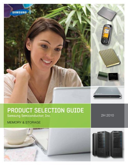
<strong>Product</strong> <strong>Selection</strong> <strong>Guide</strong><br />
<strong>Samsung</strong> Semiconductor, Inc.<br />
MeMory & Storage<br />
2H 2010
<strong>Samsung</strong> Semiconductor, inc.<br />
<strong>Samsung</strong> offers the industry’s broadest memory portfolio and has maintained its<br />
leadership in memory technology for 16 straight years. Its DraM, flash and SraM<br />
products are found in computers—from ultra-mobile portables to powerful servers—<br />
and in a wide range of handheld devices such as smartphones and MP3 players.<br />
<strong>Samsung</strong> also delivers the industry’s widest line of storage products. these include<br />
optical and hard disk drives as well as flash storage, such as the all-flash Solid State<br />
Drive and a range of embedded and removable flash storage products.<br />
Markets drAM SrAM FlASH ASic loGic tFt/lcd odd/Hdd<br />
Mobile/Wireless<br />
Notebook PCs<br />
Desktop<br />
PCs/Workstations<br />
Servers<br />
Networking/<br />
Communications<br />
Consumer<br />
Electronics<br />
www.samsung.com/us/business/components
drAM<br />
www.samsung.com/semi/dram<br />
• DDR3 SDRAM<br />
• DDR2 SDRAM<br />
• DDR SDRAM<br />
• SDRAM<br />
• Mobile SDRAM<br />
• RDRAM<br />
FlASH<br />
www.samsung.com/semi/flash<br />
• SLC Flash<br />
• MLC Flash<br />
• SD and microSD Cards<br />
• Flash Ordering Information<br />
HiGH SPeed SrAM<br />
www.samsung.com/semi/sram<br />
• Asychronous<br />
• Synchronous<br />
• NtRAM<br />
• Late-Write R-R SRAM<br />
• DDR / II / II+ SRAM<br />
• QDR / II / II+ SRAM<br />
Multi-cHiP PAcKAGe<br />
www.samsung.com/semi/mcp<br />
• NAND & DRAM<br />
• OneNAND & DRAM<br />
• Flex-OneNAND & DRAM<br />
• OneNAND & DRAM & OneDRAM<br />
• moviNAND & NAND & DRAM<br />
Fusion Memory<br />
www.samsung.com/semi/fusion<br />
• moviNAND<br />
• OneDRAM<br />
StorAGe<br />
HaManufacturers SSD<br />
repsr• Flash<br />
Solid www.samsungssd.com<br />
State Drives<br />
Optical • SATA SSD Disk Drives<br />
www.samsungodd.com<br />
Hard Drive<br />
• External DVD<br />
www.samsung.com/hdd<br />
• Internal DVD<br />
• Internal COMBO<br />
Pages 4-13<br />
• Graphics DDR SDRAM<br />
• DRAM Ordering Information<br />
• NOR & UtRAM<br />
• NOR & DRAM<br />
Pages 14-16<br />
Pages 17-20<br />
Pages 21-22<br />
Pages 23<br />
Pages 24-27<br />
• Optical Internal Disc CD<br />
www.samsungodd.com<br />
STORAGE FUSION MCP SRAM FLASH DRAM
ddr3 SdrAM reGiStered ModuleS<br />
Density Voltage Organization Part Number Composition Compliance Speed (Mbps) Ranks <strong>Product</strong>ion<br />
1GB 1.5V 128Mx72 M393B2873FH0-C(F8/H9/K0*)(04/05) 1Gb (128M x8) * 9 Lead Free & Halogen Free 1066/1333 1 Now<br />
2GB 1.5V 256Mx72<br />
4GB 1.5V 512Mx72<br />
8GB 1.5V 1Gx72<br />
M393B5673FH0-C(F8/H9/K0*)(04/05) 1Gb (128M x8) * 18 Lead Free & Halogen Free 1066/1333 2 Now<br />
M393B5670FH0-C(F8/H9/K0*)(04/05) 1Gb (256M x4) * 18 Lead Free & Halogen Free 1066/1333 1 Now<br />
M393B5173FH0-CF8(04/05) 1Gb (128M x8) * 36 Lead Free & Halogen Free 1066/1333 4 Now<br />
M393B5170FH0-C(F8/H9/K0*)(04/05) 1Gb (256M x4) * 36 Lead Free & Halogen Free 1066/1333 2 Now<br />
M393B5273CH0-C(F8/H9/K0*)(04/05) 2Gb (256M x8) * 18 Lead Free & Halogen Free 1066/1333 2 Now<br />
M393B5270CH0-C(F8/H9/K0*)(04/05) 2Gb (512M x4) * 18 Lead Free & Halogen Free 1066/1333 1 Now<br />
M393B1K73CH0-CF8(04/05) 2Gb (256M x8) * 36 Lead Free & Halogen Free 1066/1333 4 Now<br />
M393B1K70CH0-C(F8/H9/K0*)(04/05) 2Gb (512M x4) * 36 Lead Free & Halogen Free 1066/1333 2 Now<br />
16GB 1.5V 2Gx72 M393B2K70CM0-CF8(04/05) 4Gb DDP (1024M x4) * 36 Lead Free & Halogen Free 1066/1333 4 Now<br />
32GB 1.5V 4Gx72 M393B4G70AM0-CF8(04/05) 8Gb DDP (2048M x4) * 36 Lead Free & Halogen Free 1066/1333 4 Now<br />
1GB 1.35V 128Mx72 M393B2873FH0-Y(F8/H9/K0*)(04/05) 1Gb (128M x8) * 9 Lead Free & Halogen Free 1066/1333 1 Now<br />
2GB 1.35V 256Mx72<br />
4GB 1.35V 512Mx72<br />
8GB 1.35V 1Gx72<br />
M393B5673FH0-Y(F8/H9/K0*)(04/05) 1Gb (128M x8) * 18 Lead Free & Halogen Free 1066/1333 2 Now<br />
M393B5670FH0-Y(F8/H9/K0*)(04/05) 1Gb (256M x4) * 18 Lead Free & Halogen Free 1066/1333 1 Now<br />
M393B5173FH0-YF8(04/05) 1Gb (128M x8) * 36 Lead Free & Halogen Free 1066/1333 4 Now<br />
M393B5170FH0-Y(F8/H9/K0*)(04/05) 1Gb (256M x4) * 36 Lead Free & Halogen Free 1066/1333 2 Now<br />
M393B5273CH0-Y(F8/H9/K0*)(04/05) 2Gb (256M x8) * 18 Lead Free & Halogen Free 1066/1333 2 Now<br />
M393B5270CH0-Y(F8/H9/K0*)(04/05) 2Gb (512M x4) * 18 Lead Free & Halogen Free 1066/1333 1 Now<br />
M393B1K73CH0-YF8(04/05) 2Gb (256M x8) * 36 Lead Free & Halogen Free 1066/1333 4 Now<br />
M393B1K70CH0-Y(F8/H9/K0*)(04/05) 2Gb (512M x4) * 36 Lead Free & Halogen Free 1066/1333 2 Now<br />
16GB 1.35V 2Gx72 M393B2K70CM0-YF8(04/05) 4Gb DDP (1024M x4) * 36 Lead Free & Halogen Free 1066/1333 4 Now<br />
32GB 1.35V 4Gx72 M393B4G70AM0-YF8(04/05) 8Gb DDP (2048M x4) * 36 Lead Free & Halogen Free 1066/1333 4 Now<br />
Notes: F7 = DDR3-800 (6-6-6)<br />
F8 = DDR3-1066 (7-7-7)<br />
H9 = DDR3-1333 (9-9-9)<br />
K0 = DDR3-1600 (11-11-11)<br />
04 = IDt B0 register<br />
05 = Inphi C0 register<br />
* K0 (1600Mbps) available in es only<br />
4 DDR3 SDRAM<br />
2H 2010<br />
www.samsung.com/semi/dram
ddr3 SdrAM VlP reGiStered ModuleS<br />
Density Voltage Organization Part Number Composition Compliance Speed (Mbps) Ranks <strong>Product</strong>ion<br />
1GB 1.5V 128Mx72 M392B2873FH0-C(F8/H9)(04/05) 1Gb (128M x8) * 9 Lead Free & Halogen Free 1066/1333 1 Now<br />
2GB 1.5V 256Mx72<br />
4GB 1.5V 512Mx72<br />
8GB 1.5V 1Gx72<br />
M392B5673FH0-C(F8/H9)(04/05) 1Gb (128M x8) * 18 Lead Free & Halogen Free 1066/1333 2 Now<br />
M392B5670FH0-C(F8/H9)(04/05) 1Gb (256M x8) * 18 Lead Free & Halogen Free 1066/1333 1 Now<br />
M392B5170FM0-C(F8/H9)(04/05) 2Gb DDP (512M x4) * 18 Lead Free & Halogen Free 1066/1333 2 Now<br />
M392B5273CH0-C(F8/H9)(04/05) 2Gb (256M x8) * 18 Lead Free & Halogen Free 1066/1333 2 Now<br />
M392B5270CH0-C(F8/H9)(04/05) 2Gb (512M x4) * 18 Lead Free & Halogen Free 1066/1333 1 Now<br />
M392B1K73CM0-CF8(04/05) 4Gb DDP (512M x8) * 18 Lead Free & Halogen Free 1066/1333 4 Now<br />
M392B1K70CM0-C(F8/H9)(04/05) 4Gb DDP (1024M x4) * 18 Lead Free & Halogen Free 1066/1333 2 Now<br />
16GB 1.5V 2Gx72 M392B2G70AM0-C(F8/H9)(04/05) 8Gb DDP (2048M x4) * 18 Lead Free & Halogen Free 1066/1333 2 Now<br />
1GB 1.35V 128Mx72 M392B2873FH0-Y(F8/H9)(04/05) 1Gb (128M x8) * 9 Lead Free & Halogen Free 1066/1333 1 Now<br />
2GB 1.35V 256Mx72<br />
4GB 1.35V 512Mx72<br />
8GB 1.35V 1Gx72<br />
M392B5673FH0-Y(F8/H9)(04/05) 1Gb (128M x8) * 18 Lead Free & Halogen Free 1066/1333 2 Now<br />
M392B5670FH0-Y(F8/H9)(04/05) 1Gb (256M x8) * 18 Lead Free & Halogen Free 1066/1333 1 Now<br />
M392B5170FM0-Y(F8/H9)(04/05) 2Gb DDP (512M x4) * 18 Lead Free & Halogen Free 1066/1333 2 Now<br />
M392B5273CH0-Y(F8/H9)(04/05) 2Gb (256M x8) * 18 Lead Free & Halogen Free 1066/1333 2 Now<br />
M392B5270CH0-Y(F8/H9)(04/05) 2Gb (512M x4) * 18 Lead Free & Halogen Free 1066/1333 1 Now<br />
M392B1K73CM0-YF8(04/05) 4Gb DDP (512M x8) * 18 Lead Free & Halogen Free 1066/1333 4 Now<br />
M392B1K70CM0-Y(F8/H9)(04/05) 4Gb DDP (1024M x4) * 18 Lead Free & Halogen Free 1066/1333 2 Now<br />
16GB 1.35V 2Gx72 M392B2G70AM0-Y(F8/H9)(04/05) 8Gb DDP (2048M x4) * 18 Lead Free & Halogen Free 1066/1333 2 Now<br />
Notes: F7 = DDR3-800 (6-6-6)<br />
F8 = DDR3-1066 (7-7-7)<br />
H9 = DDR3-1333 (9-9-9)<br />
04 = IDt B0 register<br />
05 = Inphi C0 register<br />
ddr3 SdrAM unBuFFered ModuleS<br />
Density Voltage Organization Part Number Composition Compliance Speed (Mbps) Ranks <strong>Product</strong>ion<br />
1GB 1.5V 128Mx64 M378B2873FH0-C(F8/H9/K0*) 1Gb (128M x8) * 8 Lead Free & Halogen Free 1066/1333/1600 1 Now<br />
2GB 1.5V 256Mx64<br />
M378B5673FH0-C(F8/H9/K0*)<br />
M378B5773FH0-C(F8/H9/K0*)<br />
1Gb (128M x8) * 16<br />
2Gb (256M x8) * 8<br />
Lead Free & Halogen Free<br />
Lead Free & Halogen Free<br />
1066/1333/1600<br />
1066/1333/1600<br />
2<br />
1<br />
Now<br />
Now<br />
4GB 1.5V 512Mx64 M378B5273CH0-C(F8/H9/K0*) 2Gb (256M x8) * 16 Lead Free & Halogen Free 1066/1333/1600 2 Now<br />
8GB 1.5V 1024Mx64 M378B1G73AH0-C(F8/H9/K0*) 4Gb (512M x8) * 16 Lead Free & Halogen Free 1066/1333/1600 2 Now<br />
ddr3 SdrAM unBuFFered ModuleS (ecc)<br />
Density Voltage Organization Part Number Composition Compliance Speed (Mbps) Ranks <strong>Product</strong>ion<br />
1GB 1.5V 128Mx72 M391B2873FH0-C(F8/H9/K0*) 1Gb (128M x8) * 9 Lead Free & Halogen Free 1066/1333/1600 1 Now<br />
2GB 1.5V 256Mx72<br />
M391B5673FH0-C(F8/H9/K0*)<br />
M391B5773FH0-C(F8/H9/K0*)<br />
1Gb (128M x8) * 18<br />
2Gb (256M x8) * 9<br />
Lead Free & Halogen Free<br />
Lead Free & Halogen Free<br />
1066/1333/1600<br />
1066/1333/1600<br />
2<br />
1<br />
Now<br />
Now<br />
4GB 1.5V 512Mx72 M391B5273CH0-C(F8/H9/K0*) 2Gb (256M x8) * 18 Lead Free & Halogen Free 1066/1333/1600 2 Now<br />
8GB 1.5V 1024Mx72 M391B1G73AH0-C(F8/H9/K0*) 4Gb (512M x8) * 18 Lead Free & Halogen Free 1066/1333/1600 2 Now<br />
1GB 1.35V 128Mx72 M391B2873FH0-Y(F8/H9/K0*) 1Gb (128M x8) * 9 Lead Free & Halogen Free 1066/1333/1600 1 Now<br />
2GB 1.35V 256Mx72<br />
M391B5673FH0-Y(F8/H9/K0*)<br />
M391B5773FH0-Y(F8/H9/K0*)<br />
1Gb (128M x8) * 18<br />
2Gb (256M x8) * 9<br />
Lead Free & Halogen Free<br />
Lead Free & Halogen Free<br />
1066/1333/1600<br />
1066/1333/1600<br />
2<br />
1<br />
Now<br />
Now<br />
4GB 1.35V 512Mx72 M391B5273CH0-Y(F8/H9/K0*) 2Gb (256M x8) * 18 Lead Free & Halogen Free 1066/1333/1600 2 Now<br />
8GB 1.35V 1024Mx72 M391B1G73AH0-Y(F8/H9/K0*) 4Gb (512M x8) * 18 Lead Free & Halogen Free 1066/1333/1600 2 Now<br />
Notes: F7 = DDR3-800 (6-6-6)<br />
F8 = DDR3-1066 (7-7-7)<br />
H9 = DDR3-1333 (9-9-9)<br />
K0 = DDR3-1600 (11-11-11)<br />
* K0 (1600Mbps) available in es only<br />
www.samsung.com/semi/dram 2H 2010<br />
DDR3 SDRAM<br />
5<br />
DRAM
ddr3 SdrAM SodiMM ModuleS<br />
Density Voltage Organization Part Number Composition Compliance Speed (Mbps) Ranks <strong>Product</strong>ion<br />
1GB 1.5V 128Mx64 M471B2873FHS-C(F8/H9/K0*) 1Gb (128M x8) * 8 Lead Free & Halogen Free 1066/1333/1600 1 Now<br />
2GB 1.5V 256Mx64<br />
M471B5673FH0-C(F8/H9/K0*)<br />
M471B5773FHS-C(F8/H9/K0*)<br />
1Gb (128M x8) * 16<br />
2Gb (256M x8) * 8<br />
Lead Free & Halogen Free<br />
Lead Free & Halogen Free<br />
1066/1333/1600<br />
1066/1333/1600<br />
2<br />
1<br />
Now<br />
Now<br />
4GB 1.5V 512Mx64 M471B5273CH0-C(F8/H9/K0*) 2Gb (256M x8) * 16 Lead Free & Halogen Free 1066/1333/1600 2 Now<br />
8GB 1.5V 1024Mx64 M471B1G73AH0-C(F8/H9/K0*) 4Gb (512M x8) * 16 Lead Free & Halogen Free 1066/1333/1600 2 Now<br />
1GB 1.35V 128Mx64 M471B2873FHS-Y(F8/H9/K0*) 1Gb (128M x8) * 8 Lead Free & Halogen Free 1066/1333/1600 1 Now<br />
2GB 1.35V 256Mx64<br />
M471B5673FH0-Y(F8/H9/K0*)<br />
M471B5773FHS-Y(F8/H9/K0*)<br />
1Gb (128M x8) * 16<br />
2Gb (256M x8) * 8<br />
Lead Free & Halogen Free<br />
Lead Free & Halogen Free<br />
1066/1333/1600<br />
1066/1333/1600<br />
2<br />
1<br />
Now<br />
Now<br />
4GB 1.35V 512Mx64 M471B5273CH0-Y(F8/H9/K0*) 2Gb (256M x8) * 16 Lead Free & Halogen Free 1066/1333/1600 2 Now<br />
8GB 1.35V 1024Mx64 M471B1G73AH0-Y(F8/H9/K0*) 4Gb (512M x8) * 16 Lead Free & Halogen Free 1066/1333/1600 2 Now<br />
Notes: F7 = DDR3-800 (6-6-6)<br />
F8 = DDR3-1066 (7-7-7)<br />
H9 = DDR3-1333 (9-9-9)<br />
ddr3 SdrAM coMPonentS<br />
Density Voltage Organization Part Number # Pins-Package Compliance Speed (Mbps) Dimensions <strong>Product</strong>ion<br />
1Gb 1.5V<br />
2Gb 1.5V<br />
1Gb 1.35V<br />
2Gb 1.35V<br />
Notes: F7 = DDR3-800 (6-6-6)<br />
F8 = DDR3-1066 (7-7-7)<br />
H9 = DDR3-1333 (9-9-9)<br />
K0 = DDR3-1600 (11-11-11)<br />
ddr2 SdrAM reGiStered ModuleS<br />
Density Organization Part Number Composition Compliance Speed (Mbps) Register Rank <strong>Product</strong>ion<br />
1GB 128Mx72 M393T2863FBA-C(E6/F7) (128M x8)*9 Lead free 667/800 Y 1 Now<br />
2GB 256Mx72<br />
256M x4 K4B1G0446F-HC(F8/H9) 78 Ball -FBGA Lead Free & Halogen Free 1066/1333 7.5x11mm Now<br />
128M x8 K4B1G0846F-HC(F8/H9/K0*) 78 Ball -FBGA Lead Free & Halogen Free 1066/1333/1600 7.5x11mm Now<br />
512M x4 K4B2G0446C-HC(F8/H9) 78 Ball -FBGA Lead Free & Halogen Free 1066/1333 7.5x11mm Now<br />
256M x8 K4B2G0846C-HC(F8/H9/K0*) 78 Ball -FBGA Lead Free & Halogen Free 1066/1333/1600 7.5x11mm Now<br />
128M x16 K4B2G1646C-HC(F8/H9/K0*/MA*/NB*) 96 Ball -FBGA Lead Free & Halogen Free 1066/1333/1600 7.5x13.3mm Now<br />
256M x4 K4B1G0446F-HC(F8/H9) 78 Ball -FBGA Lead Free & Halogen Free 1066/1333 7.5x11mm Now<br />
128M x8 K4B1G0846F-HC(F8/H9/K0*) 78 Ball -FBGA Lead Free & Halogen Free 1066/1333/1600 7.5x11mm Now<br />
512M x4 K4B2G0446C-HC(F8/H9) 78 Ball -FBGA Lead Free & Halogen Free 1066/1333 7.5x11mm Now<br />
256M x8 K4B2G0846C-HC(F8/H9/K0*) 78 Ball -FBGA Lead Free & Halogen Free 1066/1333/1600 7.5x11mm Now<br />
M393T5660FBA-C(E6/F7) (256M x4)*18 Lead free 667/800 Y 1 Now<br />
M393T5663FBA-C(E6/E7) (128M x8)*18 Lead free 667/800 Y 2 Now<br />
4GB 512Mx72 M393T5160FBA-C(E6/F7) (256M x4)*36 Lead free 667/800 Y 2 Now<br />
Notes: e6=PC2-5300 (DDR2-667 @ CL=5)<br />
F7=PC2-6400 (DDR2-800 @ CL=6)<br />
e7=PC2-6400 (DDR2-800 @ CL=5)<br />
Voltage = 1.8V<br />
K0 = DDR3-1600 (11-11-11)<br />
* K0 (1600Mbps) available in es only<br />
MA = DDR3-1866 (13-13-13)<br />
NB = DDR3-2133 (14-14-14)<br />
* K0, MA, and NB are available in es only<br />
ddr2 SdrAM VlP reGiStered ModuleS<br />
Density Organization Part Number Composition Compliance Speed (Mbps) Register Rank <strong>Product</strong>ion<br />
2GB 256Mx72 M392T5660FBA-CE6 (256M x4)*18 Lead free 667 Y 1<br />
6 DDR3 & DDR2 SDRAM<br />
2H 2010 www.samsung.com/semi/dram
ddr2 SdrAM FullY BuFFered ModuleS<br />
Density Organization Part Number Composition Compliance Speed (Mbps) Voltage Rank <strong>Product</strong>ion<br />
2GB 256Mx72 M395T5663FB4-CE68 (128M x8)*18 Lead free 667 1.8V 2 Now<br />
4GB<br />
512Mx72 M395T5160FB4-CE68 (256M x4)*36 Lead free 667 1.8V 2 Now<br />
512Mx72 M395T5163FB4-CE68 (128M x8)*36 Lead free 667 1.8V 4 Now<br />
Notes: e6 = PC2-5300 (DDR2-667 @ CL=5)<br />
AMB = IDt L4<br />
Voltage = 1.8V (AMB Voltage = 1.5V)<br />
ddr2 SdrAM unBuFFered ModuleS<br />
Density Organization Part Number Composition Compliance Speed (Mbps) Rank <strong>Product</strong>ion<br />
1GB 128Mx64 M378T2863FBS-C(E6/F7/E7) (128M x8)*8 Lead free 667/800 1 Now<br />
2GB 256Mx64 M378T5663FB3-C(E6/F7/E7) (128M x8)*16 Lead free 667/800 2 Now<br />
Notes: e6=PC2-5300 (DDR2-667 @ CL=5)<br />
e7=PC2-6400 (DDR2-800 @ CL=5)<br />
F7=PC2-6400 (DDR2-800 @ CL=6)<br />
Voltage = 1.8V<br />
ddr2 SdrAM unBuFFered ModuleS (ecc)<br />
Density Organization Part Number Composition Compliance Speed (Mbps) Rank <strong>Product</strong>ion<br />
1GB 128Mx72 M391T2863FB3-C(E6/F7) (128Mx8)*9 Lead free 667/800 1 Now<br />
2GB 256Mx64 M391T5663FB3-C(E6/F7) (128Mx8)*18 Lead free 667/800 2 Now<br />
Notes: e6=PC2-5300 (DDR2-667 @ CL=5)<br />
e7=PC2-6400 (DDR2-800 @ CL=5)<br />
F7=PC2-6400 (DDR2-800 @ CL=6)<br />
Voltage = 1.8V<br />
ddr2 SdrAM SodiMM ModuleS<br />
Density Organization Part Number Composition Compliance Speed (Mbps) Rank <strong>Product</strong>ion<br />
1GB 128Mx64 M470T2863FB3-C(E6/F7/E7) (64Mx16)*8 Lead free 667/800 2 Now<br />
2GB 256Mx64 M470T5663FB3-C(E6/F7/E7) (128M x8)*8 Lead free 667/800 2 Now<br />
Notes: e6=PC2-5300 (DDR2-667 @ CL=5)<br />
e7=PC2-6400 (DDR2-800 @ CL=5)<br />
F7=PC2-6400 (DDR2-800 @ CL=6)<br />
Voltage = 1.8V<br />
ddr2 SdrAM coMPonentS<br />
Density Organization Part Number # Pins-Package Dimensions Package Speed (Mbps) <strong>Product</strong>ion<br />
256Mb 16Mx16 K4T56163QN-HC(E6/F7/E7/F8) 84-FBGA 7.5x12.5mm Lead free & Halogen free 667/800/1066 Now<br />
128M x4 K4T51043QI-HC(E6/F7/E7) 60-FBGA 7.5x9.5mm Lead free & Halogen free 667/800 Now<br />
64M x8 K4T51083QI-HC(E6/F7/E7/F8) 60-FBGA 7.5x9.5mm Lead free & Halogen free 667/800/1066 Now<br />
512Mb<br />
32M x16<br />
128M x4<br />
K4T51163QI-HC(E6/F7/E7/F8)<br />
K4T51043QJ-HC(E6/F7/E7)<br />
84-FBGA<br />
60-FBGA<br />
7.5x12.5mm<br />
7.5x9.5mm<br />
Lead free & Halogen free<br />
Lead free & Halogen free<br />
667/800/1066<br />
667/800<br />
Now<br />
Q3<br />
64M x8 K4T51083QJ-HC(E6/F7/E7/F8) 60-FBGA 7.5x9.5mm Lead free & Halogen free 667/800/1066 Q3<br />
32M x16 K4T51163QJ-HC(E6/F7/E7/F8) 84-FBGA 7.5x12.5mm Lead free & Halogen free 667/800/1066 Q3<br />
256M x4 K4T1G044QF-BC(E6/F7/E7) 68-FBGA 7.5x9.5mm Lead free & Halogen free 667/800 Now<br />
1Gb 128M x8 K4T1G084QF-BC(E6/F7/E7/F8) 68-FBGA 7.5x9.5mm Lead free & Halogen free 667/800/1066 Now<br />
64M x16 K4T1G164QF-BC(E6/F7/E7/F8) 84-FBGA 7.5x12.5mm Lead free & Halogen free 667/800/1066 Now<br />
Notes: e6=DDR2-667 (5-5-5)<br />
F7=DDR2-800 (6-6-6)<br />
e7=DDR2-800 (5-5-5)<br />
F8=DDR2-1066 (7-7-7)<br />
Voltage = 1.8V<br />
www.samsung.com/semi/dram 2H 2010<br />
DDR2 SDRAM<br />
7<br />
DRAM
ddr SdrAM 1u reGiStered ModuleS<br />
Density Organization Part Number Composition Speed (Mbps)<br />
1GB 128Mx72 M312L2920GH3-CB3 (128Mx4)*18 333/400<br />
2GB 256Mx72 M312L5720GH3-CB3 (128Mx4)*36 333/400<br />
Notes: B0 = DDR266 (133MHz @ CL=2.5)<br />
A2 = DDR266 (133MHz @ Cl=2)<br />
B3 = DDR333 (166MHz @ CL=2.5)<br />
CC = DDR400 (200MHz @ CL=3)<br />
type: 184-pin<br />
ddr drAM SodiMM ModuleS<br />
Density Organization Part Number Composition Speed (Mbps)<br />
512MB 64Mx64 M470L6524GL0-CB300 (32M x 16)*8 333<br />
Notes: B0 = DDR266 (133MHz @ CL=2.5)<br />
CC = DDR400 (200MHz @ CL=3)<br />
B3 = DDR333 (166MHz @ CL=2.5)<br />
A2 = DDR266 (133MHz @ Cl=2)<br />
ddr SdrAM coMPonentS<br />
Density Organization Part Number # Pins - Package Speed (Mbps)<br />
256Mb<br />
512Mb<br />
64Mx4 K4H560438N-LCB3/B0 66-TSOP 266/333<br />
32Mx8 K4H560838N-LCCC/B3 66-TSOP 333/400<br />
16Mx16 K4H561638N-LCCC/B3 66-TSOP 333/400<br />
128Mx4<br />
64Mx8<br />
K4H510438G-LCB3/B0 66-TSOP 266/333<br />
K4H510438G-HCCC/B3 60-FBGA 333/400<br />
K4H510838G-LCCC/B3 66-TSOP 333/400<br />
K4H510838G-HCCC/B3 60-FBGA 333/400<br />
32Mx16 K4H511638G-LCCC/B3 66-TSOP 333/400<br />
128Mb 8Mx16 K4H281638O-LCCC 66-TSOP 400<br />
Notes: B0 = DDR266 (133MHz @ CL=2.5)<br />
A2 = DDR266 (133MHz @ Cl=2)<br />
B3 = DDR333 (166MHz @ CL=2.5)<br />
CC = DDR400 (200MHz @ CL=3)<br />
8 DDR<br />
2H 2010 www.samsung.com/semi/dram
SdrAM coMPonentS<br />
Density Organization Part Number # Pins - Package Speed (Mbps) Refresh Remarks<br />
64Mb<br />
128Mb<br />
256Mb<br />
512Mb<br />
8Mx8 K4S640832N-LC75000 54-TSOP 133 4K EOL with no replacement<br />
4Mx16 K4S641632N-LC(L)(75/60)000 54-TSOP 133/166 4K EOL with no replacement<br />
16Mx8 K4S280832O-LC(L)75000 54-TSOP 133 4K<br />
8Mx16 K4S281632O-LC(L)(75/60)000 54-TSOP 133/166 4K<br />
64Mx4 K4S560432N-LC(L)75000 54-TSOP 133 8K<br />
32Mx8 K4S560832N-LC(L)75000 54-TSOP 133 8K<br />
16Mx16 K4S561632N-LC(L)(75/60)000 54-TSOP 133/166 8K<br />
128Mx4 K4S510432D-UC(L)(75)000 54-TSOP 133 8K EOL with no replacement<br />
64Mx8 K4S510832D-UC(L)(75)000 54-TSOP 133 8K EOL with no replacement<br />
32Mx16 K4S511632D-UC(L)(75)000 54-TSOP 133 8K EOL with no replacement<br />
Notes: L = Commercial temp., Low Power<br />
For Industrial temperature, check with ssI Marketing<br />
Banks: 4<br />
rdrAM coMPonentS<br />
All products are Lead Free<br />
Voltage: 3.3V<br />
speed: PC133 (133MHz CL=3/PC100 CL2)<br />
Density Organization Part Number Speed (Mbps) # Pins-Package Refresh Note<br />
288M x18 K4R881869I-DCT9000 1066 92-FBGA 16K/32ms EOL in Aug'10<br />
Notes: All products are lead free<br />
GrAPHicS drAM coMPonentS<br />
Type Density Organization Part Number Package VDD/VDDQ Speed Bin (MHz) Status<br />
GDDR5 1Gb 32Mx32 K4G10325FE-HC(1) 170-FBGA 1.5/1.5V 1800/2000/2500<br />
GDDR3<br />
GDDR2<br />
GDDR1 128Mb<br />
1Gb 32Mx32 K4J10324KE-HC(1) 136-FBGA 1.8V/1.8V 700/800/1000/1200<br />
512Mb 16Mx32<br />
K4J52324QH-HC(1) 136-FBGA 1.8/1.8V 700/800 EOL Mar '10<br />
K4J52324QH-HJ(1) 136-FBGA 1.9/1.9V 1000 EOL Mar '10<br />
K4J52324QH-HJ(1) 136-FBGA 2.05/2.05V 1200 EOL Mar '10<br />
1Gb 64Mx16 K4N1G164QE-HC(1) 84-FBGA 1.8/1.8V 400/500 EOL Mar '10<br />
512Mb 32Mx16 K4N51163QG-HC(1) 84-FBGA 1.8/1.8V 400/500 EOL Mar '10<br />
4Mx32<br />
Notes: Package:<br />
Q: tQFP<br />
U: tQFP (Lead Free)<br />
G: 84/144 FBGA<br />
V: 144 FBGA (Lead Free)<br />
Z: 84 FBGA (Lead Free)<br />
t: tsoP<br />
L: tsoP (Lead Free)<br />
A: 136 FBGA<br />
B: 136 FBGA (Lead Free)<br />
H: FBGA (Halogen Free & Lead Free)<br />
e: 100 FBGA (Halogen Free & Lead Free)<br />
K4D263238K-VC(1) 144-FBGA 2.5/2.5V 200/250 CuSmpl Oct '09<br />
K4D263238K-UC(1) 100-TQFP 2.5/2.5V 200/250<br />
8Mx16 K4D261638K-LC(1) 66-TSOPII 2.5/2.5V 200/250 EOL Sep '10<br />
(1) Speeds (clock cycle - speed bin):<br />
04: 0.4ns (2500MHz)<br />
05: 0.5ns (2000MHz)<br />
5C: 0.555 (1800MHz)<br />
07: 0.71ns (1400MHz)<br />
08: 0.83ns (1200MHz)<br />
09: 0.90ns (1100MHz)<br />
1A: 1ns (1000MHz)<br />
11: 1.1ns (900MHz)<br />
12: 1.25ns (800MHz)<br />
14: 1.429ns (700MHz)<br />
16: 1.667ns (600MHz)<br />
20: 2.0ns (500MHz)<br />
22: 2.2ns (450MHz)<br />
25: 2.5ns (400MHz)<br />
2A: 2.86ns (350MHz)<br />
33: 3.3ns (300MHz)<br />
40: 4.0ns (240MHz)<br />
50: 5.0ns (200MHz)<br />
www.samsung.com/semi/dram 2H 2010<br />
SDRAM, RDRAM & Graphics DRAM Components<br />
9<br />
DRAM
MoBile-Sdr/ddr<br />
Density Type Organization Part Number Package Power <strong>Product</strong>ion<br />
256Mb<br />
512Mb<br />
MSDR<br />
MDDR<br />
MSDR<br />
MDDR<br />
1Gb MDDR<br />
2Gb MDDR<br />
4Gb MDDR<br />
lPddr2<br />
16Mx16 K4M56163PN-BG(1) 54-FBGA 1.8V Now<br />
8Mx32 K4M56323PN-HG(1) 90-FBGA 1.8V Now<br />
16Mx16 K4X56163PN-FG(1) 60-FBGA 1.8V Now<br />
8Mx32 K4X56323PN-8G(1) 90-FBGA 1.8V Now<br />
32Mx16 K4M51163PI-BG(1) 54-FBGA 1.8V Now<br />
16Mx32 K4M51323PI-HG(1) 90-FBGA 1.8V Now<br />
32Mx16 K4X51163PI-FG(1) 60-FBGA 1.8V Now<br />
16Mx32 K4X51323PI-8G(1) 90-FBGA 1.8V Now<br />
64Mx16 K4X1G163PE-FG(1) 60-FBGA 1.8V Now<br />
32Mx32 K4X1G323PE-8G(1) 90-FBGA 1.8V Now<br />
64Mx16 K4X1G163PF-FG(1) 60-FBGA 1.8V MP Q1'11<br />
32Mx32 K4X1G323PF-8G(1) 90-FBGA 1.8V MP Q1'11<br />
128Mx16 K4X2G163PC-FG(1) 60-FBGA 1.8V Now<br />
64Mx32 K4X2G323PC-8G(1) 90-FBGA 1.8V Now<br />
x32 (2CS, 2CKE) K4X4G303PB-AG(1) 168-FBGA, 12x12 PoP, DDP 1.8V Now<br />
x32 (2CS, 2CKE) K4X4G303PB-AG(1) 168-FBGA, 12x12 PoP, DDP 1.8V Now<br />
x32 (2CS, 2CKE) K4X4G303PB-7G(1) 240-FBGA, 14x14 PoP, DDP 1.8V Now<br />
Density Type Organization Part Number Package Power <strong>Product</strong>ion<br />
512Mb LPDDR2 1CH x32 K4P51323EI-AG(1) 168-FBGA, 12x12 PoP 1.8V Now<br />
1Gb LPDDR2 1CH x32 K4P1G324EE-AG(1) 168-FBGA, 12x12 PoP 1.2V Now<br />
2Gb LPDDR2<br />
4Gb LPDDR2<br />
1CH x32 K4P2G324EC-AG(1) 168-FBGA, 12x12 PoP 1.2V Now<br />
2CH x32/ch<br />
K3PE3E300M-XG(1) 216-FBGA, 12x12 PoP 1.2V Now<br />
K3PE3E300A-XG(1) 240-FBGA, 14x14 PoP 1.2V Now<br />
1CH x32 K4P4G304EC-AG(1) 168-FBGA, 12x12 PoP, DDP 1.2V Now<br />
2CH x32/ch<br />
K3PE4E400M-XG(1) 216-FBGA, 12x12 PoP, DDP 1.2V Now<br />
K3PE4E400M-XG(1) 216-FBGA, 12x12 PoP, DDP 1.2V Now<br />
K3PE4E400A-XG(1) 240-FBGA, 14x14 PoP, DDP 1.2V Now<br />
Notes: All products offered at extended, Low, i-tCsR & PAsR & Ds (temp, Power) (1) Speed:<br />
Mobile-SDR<br />
60: 166MHz, CL3<br />
75: 133MHz, CL3<br />
Mobile-DDR<br />
D8: 200MHz, CL3<br />
C6: 166MHz, CL3<br />
LPDDR2<br />
C0: 667Mbps<br />
C1: 800Mbps<br />
10 Mobile SDR/DDR & LPDDR2<br />
2H 2010 www.samsung.com/semi/dram
coMPonent drAM orderinG inForMAtion<br />
SAMSUNG Memory<br />
DRAM<br />
DRAM Type<br />
Density<br />
Bit Organization<br />
1. Memory (K)<br />
2. DRAM: 4<br />
3. DRAM Type<br />
B: DDR3 SDRAM<br />
D: GDDR SDRAM<br />
G: GDDR5 SDRAM<br />
H: DDR SDRAM<br />
J: GDDR3 SDRAM<br />
M: Mobile SDRAM<br />
N: SDDR2 SDRAM<br />
S: SDRAM<br />
T: DDR SDRAM<br />
U: GDDR4 SDRAM<br />
V: Mobile DDR SDRAM Power Efficient Address<br />
W: SDDR3 SDRAM<br />
X: Mobile DDR SDRAM<br />
Y: XDR DRAM<br />
Z: Value Added DRAM<br />
4. Density<br />
10: 1G, 8K/32ms<br />
16: 16M, 4K/64ms<br />
26: 128M, 4K/32ms<br />
28: 128M, 4K/64ms<br />
32: 32M, 2K/32ms<br />
50: 512M, 32K/16ms<br />
51: 512M, 8K/64ms<br />
52: 512M, 8K/32ms<br />
54: 256M, 16K/16ms<br />
55: 256M, 4K/32ms<br />
56: 256M, 8K/64ms<br />
62: 64M, 2K/16ms<br />
64: 64M, 4K/64ms<br />
68: 768M, 8K/64ms<br />
1G: 1G, 8K/64ms<br />
2G: 2G, 8K/64ms<br />
4G: 4G, 8K/64ms<br />
5. Bit Organization<br />
02: x2<br />
04: x4<br />
06: x4 Stack (Flexframe)<br />
07: x8 Stack (Flexframe)<br />
1 2 3 4 5 6 7 8 9 10 11<br />
K 4 T XX XX X X X X X XX<br />
08: x8<br />
15: x16 (2CS)<br />
16: x16<br />
26: x4 Stack (JEDEC Standard)<br />
27: x8 Stack (JEDEC Standard)<br />
30: x32 (2CS, 2CKE)<br />
31: x32 (2CS)<br />
32: x32<br />
6. # of Internal Banks<br />
2: 2 Banks<br />
3: 4 Banks<br />
4: 8 Banks<br />
5: 16 Banks<br />
7. Interface ( VDD, VDDQ)<br />
2: LVTTL, 3.3V, 3.3V<br />
4: LVTTL, 2.5V, 2.5V<br />
5: SSTL-2 1.8V, 1.8V<br />
6: SSTL-15 1.5V, 1.5V<br />
8: SSTL-2, 2.5V, 2.5V<br />
A: SSTL, 2.5V, 1.8V<br />
F: POD-15 (1.5V,1.5V)<br />
H: SSTL_2 DLL, 3.3V, 2.5V<br />
M: LVTTL, 1.8V, 1.5V<br />
N: LVTTL, 1.5V, 1.5V<br />
P: LVTTL, 1.8V, 1.8V<br />
Q: SSTL-2 1.8V, 1.8V<br />
R: SSTL-2, 2.8V, 2.8V<br />
U: DRSL, 1.8V, 1.2V<br />
8. Revision<br />
A: 2nd Generation<br />
B: 3rd Generation<br />
C: 4th Generation<br />
D: 5th Generation<br />
E: 6th Generation<br />
F: 7th Generation<br />
G: 8th Generation<br />
H: 9th Generation<br />
I: 10th Generation<br />
J: 11th Generation<br />
K: 12th Generation<br />
M: 1st Generation<br />
N: 14th Generation<br />
Q: 17th Generation<br />
9. Package Type<br />
Speed<br />
Temp & Power<br />
Package Type<br />
Revision<br />
Interface (VDD, VDDQ)<br />
Number of Internal Banks<br />
DDR SDRAM<br />
L: TSOP II (Lead-free & Halogen-free)<br />
H: FBGA (Lead-free & Halogen-free)<br />
F: FBGA for 64Mb DDR (Lead-free & Halogen-free)<br />
6: sTSOP II (Lead-free & Halogen-free)<br />
T: TSOP II<br />
N: sTSOP II<br />
G: FBGA<br />
U: TSOP II (Lead-free)<br />
V: sTSOP II (Lead-free)<br />
Z: FBGA (Lead-free)<br />
DDR2 SDRAM<br />
Z: FBGA (Lead-free)<br />
J: FBGA DDP (Lead-free)<br />
Q: FBGA QDP (Lead-free)<br />
H: FBGA (Lead-free & Halogen-free)<br />
M: FBGA DDP (Lead-free & Halogen-free)<br />
E: FBGA QDP (Lead-free & Halogen-free)<br />
T: FBGA DSP (Lead-free & Halogen-free, Thin)<br />
DDR3 SDRAM<br />
Z: FBGA (Lead-free)<br />
H: FBGA (Halogen-free & Lead-free)<br />
Graphics Memory<br />
Q: TQFP<br />
U: TQFP (Lead Free)<br />
G: 84/144 FBGA<br />
V: 144 FBGA (Lead Free)<br />
Z: 84 FBGA(Lead Free)<br />
T: TSOP<br />
L: TSOP (Lead Free)<br />
A: 136 FBGA<br />
B: 136 FBGA(Lead Free)<br />
H: FBGA(Hologen Free & Lead Free)<br />
E: 100 FBGA(Hologen Free & Lead Free)<br />
SDRAM<br />
L TSOP II (Lead-free & Halogen-free)<br />
N: STSOP II<br />
T: TSOP II<br />
U: TSOP II (Lead-free)<br />
V: sTSOP II (Lead-free)<br />
www.samsung.com/semi/dram 2H 2010<br />
DRAM Ordering Information<br />
11<br />
DRAM
coMPonent drAM orderinG inForMAtion<br />
SAMSUNG Memory<br />
DRAM<br />
DRAM Type<br />
Density<br />
Bit Organization<br />
XDR DRAM<br />
J: BOC(LF) P: BOC<br />
Mobile DRAM<br />
Leaded / Lead Free<br />
G/A: 52balls FBGA Mono<br />
R/B: 54balls FBGA Mono<br />
X /Z: 54balls BOC Mono<br />
J /V: 60(72)balls FBGA Mono 0.5pitch<br />
L /F: 60balls FBGA Mono 0.8pitch<br />
S/D: 90balls FBGA<br />
Monolithic (11mm x 13mm)<br />
F/H: Smaller 90balls FBGA Mono<br />
Y/P: 54balls CSP DDP<br />
M/E: 90balls FBGA DDP<br />
10. Temp & Power - COMMON<br />
(Temp, Power)<br />
C: Commercial, Normal (0’C – 95’C) & Normal<br />
Power<br />
C: (Mobile Only) Commercial (-25 ~ 70’C), Normal<br />
Power<br />
J: Commercial, Medium<br />
L: Commercial, Low (0’C – 95’C) & Low Power<br />
L: (Mobile Only) Commercial, Low, i-TCSR<br />
F: Commercial, Low, i-TCSR & PASR & DS<br />
E: Extended (-25~85’C), Normal<br />
N: Extended, Low, i-TCSR<br />
G: Extended, Low, i-TCSR & PASR & DS<br />
I: Industrial, Normal (-40’C – 85’C) & Normal<br />
Power<br />
P: Industrial, Low (-40’C – 85’C) & Low Power<br />
H: Industrial, Low, i-TCSR & PASR & DS<br />
11. Speed (Wafer/Chip Biz/BGD: 00)<br />
1 2 3 4 5 6 7 8 9 10 11<br />
K 4 T XX XX X X X X X XX<br />
DDR SDRAM<br />
CC: DDR400 (200MHz @ CL=3, tRCD=3, tRP=3)<br />
B3: DDR333 (166MHz @ CL=2.5, tRCD=3,<br />
tRP=3) *1<br />
A2: DDR266 (133MHz @ CL=2 , tRCD=3, tRP=3)<br />
B0: DDR266 (133MHz @ CL=2.5, tRCD=3,<br />
tRP=3)<br />
Note 1: "B3" has compatibility with "A2" and "B0"<br />
DDR2 SDRAM<br />
CC: DDR2-400 (200MHz @ CL=3, tRCD=3,<br />
tRP=3)<br />
D5: DDR2-533 (266MHz @ CL=4, tRCD=4,<br />
tRP=4)<br />
E6: DDR2-667 (333MHz @ CL=5, tRCD=5,<br />
tRP=5)<br />
F7: DDR2-800 (400MHz @ CL=6, tRCD=6,<br />
tRP=6)<br />
E7: DDR2-800 (400MHz @ CL=5, tRCD=5,<br />
tRP=5)<br />
DDR3 SDRAM<br />
F7: DDR3-800 (400MHz @ CL=6, tRCD=6,<br />
tRP=6)<br />
F8: DDR3-1066 (533MHz @ CL=7, tRCD=7,<br />
tRP=7)<br />
G8: DDR3-1066 (533MHz @ CL=8, tRCD=8,<br />
tRP=8)<br />
H9: DDR3-1333 (667MHz @ CL=9, tRCD=9,<br />
tRP=9)<br />
K0: DDR3-1600 (800MHz @ CL=11, tRCD=11,<br />
tRP=11)<br />
Graphics Memory<br />
18: 1.8ns (550MHz)<br />
04: 0.4ns (2500MHz)<br />
20: 2.0ns (500MHz)<br />
05: 0.5ns (2000MHz)<br />
22: 2.2ns (450MHz)<br />
5C: 0.56ns (1800MHz)<br />
25: 2.5ns (400MHz)<br />
06: 0.62ns (1600MHz)<br />
2C: 2.66ns (375MHz)<br />
6A: 0.66ns (1500MHz)<br />
2A: 2.86ns (350MHz)<br />
07: 0.71ns (1400MHz)<br />
33: 3.3ns (300MHz)<br />
7A: 0.77ns (1300MHz)<br />
36: 3.6ns (275MHz)<br />
08: 0.8ns (1200MHz)<br />
40: 4.0ns (250MHz)<br />
09: 0.9ns (1100MHz)<br />
45: 4.5ns (222MHz)<br />
1 : 1.0ns (1000MHz)<br />
50/5A: 5.0ns (200MHz)<br />
1 : 1.1ns (900MHz)<br />
55: 5.5ns (183MHz)<br />
12: 1.25ns (800MHz)<br />
60: 6.0ns (166MHz)<br />
14: 1.4ns (700MHz)<br />
16: 1.6ns (600MHz)<br />
SDRAM (Default CL=3)<br />
50: 5.0ns (200MHz CL=3)<br />
60: 6.0ns (166MHz CL=3)<br />
67: 6.7ns<br />
75: 7.5ns PC133 (133MHz CL=3)<br />
XDR DRAM<br />
A2: 2.4Gbps, 36ns, 16Cycles<br />
B3: 3.2Gbps, 35ns, 20Cycles<br />
C3: 3.2Gbps, 35ns, 24Cycles<br />
C4: 4.0Gbps, 28ns, 24Cycles<br />
DS: Daisychain Sample<br />
Mobile-SDRAM<br />
60: 166MHz, CL 3<br />
75: 133MHz, CL 3<br />
80: 125MHz, CL 3<br />
1H: 105MHz, CL 2<br />
1L: 105MHz, CL 3<br />
15: 66MHz, CL 2 & 3<br />
Speed<br />
Temp & Power<br />
Package Type<br />
Revision<br />
Interface (VDD, VDDQ)<br />
Number of Internal Banks<br />
Mobile-DDR<br />
C3: 133MHz, CL 3<br />
C2: 100MHz, CL 3<br />
C0: 66MHz, CL 3<br />
Note: All of Lead-free or Halogen-free product are in<br />
compliance with RoHs<br />
12 DRAM Ordering Information<br />
2H 2010 www.samsung.com/semi/dram
Module drAM orderinG inForMAtion<br />
SAMSUNG Memory<br />
DIMM<br />
Data bits<br />
DRAM Component Type<br />
Depth<br />
Number of Banks<br />
Bit Organization<br />
1. Memory Module: M<br />
2. DIMM Type<br />
3: DIMM<br />
4: SODIMM<br />
3. Data bits<br />
12: x72 184pin Low Profile Registered DIMM<br />
63: x63 PC100 / PC133 μSODIMM with SPD for<br />
144pin<br />
64: x64 PC100 / PC133 SODIMM with SPD for<br />
144pin (Intel/JEDEC)<br />
66: x64 Unbuffered DIMM with SPD for<br />
144pin/168pin (Intel/JEDEC)<br />
68: x64 184pin Unbuffered DIMM<br />
70: x64 200pin Unbuffered SODIMM<br />
71: x64 204pin Unbuffered SODIMM<br />
74: x72 /ECC Unbuffered DIMM with SPD for<br />
168pin (Intel/JEDEC)<br />
77: x72 /ECC PLL + Register DIMM with SPD for<br />
168pin (Intel PC100)<br />
78: x64 240pin Unbuffered DIMM<br />
81: x72 184pin ECC unbuffered DIMM<br />
83: x72 184pin Registered DIMM<br />
90: x72 /ECC PLL + Register DIMM<br />
91: x72 240pin ECC unbuffered DIMM<br />
92: x72 240pin VLP Registered DIMM<br />
93: x72 240pin Registered DIMM<br />
95: x72 240pin Fully Buffered DIMM with SPD for<br />
168pin (JEDEC PC133)<br />
4. DRAM Component Type<br />
B: DDR3 SDRAM (1.5V VDD)<br />
L: DDR SDRAM (2.5V VDD)<br />
S: SDRAM<br />
T: DDR2 SDRAM (1.8V VDD)<br />
www.samsung.com/semi/dram<br />
1 2 3 4 5 6 7 8 9 10 11 12 13<br />
M X XX T XX X X X X X X XX X<br />
5. Depth<br />
09: 8M (for 128Mb/512Mb)<br />
17: 16M (for 128Mb/512Mb)<br />
16: 16M<br />
28: 128M<br />
29: 128M (for 128Mb/512Mb)<br />
32: 32M<br />
33: 32M (for 128Mb/512Mb)<br />
51: 512M<br />
52: 512M (for 512Mb/2Gb)<br />
56: 256M<br />
57: 256M (for 512Mb/2Gb)<br />
59: 256M (for 128Mb/512Mb)<br />
64: 64M<br />
65: 64M (for 128Mb/512Mb)<br />
1G: 1G<br />
1K: 1G (for 2Gb)<br />
6. # of Banks in Comp. & Interface<br />
1: 4K/64mxRef., 4Banks & SSTL-2<br />
2 : 8K/ 64ms Ref., 4Banks & SSTL-2<br />
2: 4K/ 64ms Ref., 4Banks & LVTTL (SDR Only)<br />
5: 8K/ 64ms Ref., 4Banks & LVTTL (SDR Only)<br />
5: 4Banks & SSTL-1.8V<br />
6: 8Banks & SSTL-1.8V<br />
7. Bit Organization<br />
0: x 4<br />
3: x 8<br />
4: x16<br />
6: x 4 Stack (JEDEC Standard)<br />
7: x 8 Stack (JEDEC Standard)<br />
8: x 4 Stack<br />
9: x 8 Stack<br />
8. Component Revision<br />
A: 2nd Gen.<br />
B: 3rd Gen.<br />
C: 4th Gen.<br />
D: 5th Gen.<br />
E: 6th Gen.<br />
F: 7th Gen.<br />
G: 8th Gen.<br />
M: 1st Gen.<br />
Q: 17th Gen.<br />
9. Package<br />
E: FBGA QDP (Lead-free & Halogen-free)<br />
G: FBGA<br />
H: FBGA (Lead-free & Halogen-free)<br />
J: FBGA DDP (Lead-free)<br />
M: FBGA DDP (Lead-free & Halogen-free)<br />
N: sTSOP<br />
Q: FBGA QDP (Lead-free)<br />
T: TSOP II (400mil)<br />
U: TSOP II (Lead-Free)<br />
V: sTSOP II (Lead-Free)<br />
Z: FBGA(Lead-free)<br />
10. PCB Revision<br />
0: Mother PCB<br />
1: 1st Rev<br />
2: 2nd Rev.<br />
3: 3rd Rev.<br />
4: 4th Rev.<br />
A: Parity DIMM<br />
S: Reduced PCB<br />
U: Low Profile DIMM<br />
11. Temp & Power<br />
C: Commercial Temp. (0°C ~ 95°C) & Normal<br />
Power<br />
L: Commercial Temp. (0°C ~ 95°C) & Low Power<br />
12. Speed<br />
CC: (200MHz @ CL=3, tRCD=3, tRP=3)<br />
D5: (266MHz @ CL=4, tRCD=4, tRP=4)<br />
E6: (333MHz @ CL=5, tRCD=5, tRP=5)<br />
F7: (400MHz @ CL=6, tRCD=6, tRP=6)<br />
E7: (400MHz @ CL=5, tRCD=5, tRP=5)<br />
F8: (533MHz @ CL=7, tRCD=7, tRP=7)<br />
G8: (533MHz @ CL=8, tRCD=8, tRP=8)<br />
H9: (667MHz @ CL=9, tRCD=9, tRP=9)<br />
K0: (800MHz @ CL=10, tRCD=10, tRP=10)<br />
7A: (133MHz CL=3/PC100 CL2)<br />
13. AMB Vendor for FBDIMM<br />
AMB Vendor<br />
Speed<br />
Temp & Power<br />
PCB Revision<br />
Package<br />
Component Revision<br />
0, 5: Intel<br />
1, 6, 8: IDT<br />
9: Montage<br />
Note: All of Lead-free or Halogen-free product are in<br />
compliance with RoHs<br />
2H 2010 DRAM Ordering Information<br />
13<br />
DRAM
Slc FlASH<br />
Family Density Part Number Package Type Org. Vol(V)<br />
16Gb Based<br />
8Gb Based<br />
4Gb Based<br />
16Gb Mono<br />
32Gb DDP<br />
64Gb QDP<br />
128Gb ODP<br />
14 SLC Flash<br />
2H 2010 www.samsung.com/semi/flash<br />
MOQ<br />
Tray T/R<br />
-xxxx0xx -xxx0Txx<br />
K9FAG08U0M-HCB0 BGA X8 3.3 960 1000 E/S<br />
K9FAG08S0M-HCB0 BGA X8 1.8 960 1000 E/S<br />
K9KBG08U1M-HCB0 BGA X8 3.3 960 1000 E/S<br />
K9KBG08S1M-HCB0 BGA X8 1.8 960 1000 E/S<br />
K9WCG08U5M-HCB0 BGA X8 3.3 960 1000 E/S<br />
K9WCG08S5M-HCB0 BGA X8 1.8 960 1000 E/S<br />
K9QDG08U5M-HCB0 BGA X8 3.3 960 1000 E/S<br />
K9QDG08S5M-HCB0 BGA X8 1.8 960 1000 E/S<br />
64Gb DSP K9NCG08U5M-PCK0 TSOP1 x8 3.3 960 1000 M/P<br />
32Gb QDP<br />
16Gb DDP<br />
8Gb Mono<br />
16Gb QDP<br />
8Gb DDP<br />
4Gb Mono<br />
2Gb Based 2Gb Mono<br />
1Gb Based 1Gb Mono<br />
512Mb Based 512Mb Mono<br />
256Mb Based 256Mb Mono<br />
K9WBG08U1M-PCB0 TSOP1 x8 3.3 960 1000 M/P<br />
K9WBG08U1M-PIB0 TSOP1 x8 3.3 960 1000 M/P<br />
K9KAG08U0M-PCB0 TSOP1 x8 3.3 960 1000 M/P<br />
K9KAG08U0M-PIB0 TSOP1 x8 3.3 960 1000 M/P<br />
K9F8G08U0M-PCB0 TSOP1 x8 3.3 960 1000 M/P<br />
K9F8G08U0M-PIB0 TSOP1 x8 3.3 960 1000 M/P<br />
K9WAG08U1D-SCB0 TSOP1 HF&LF x8 3.3 960 1000 C/S<br />
K9WAG08U1D-SIB0 TSOP1 HF&LF x8 3.3 960 1000 C/S<br />
K9WAG08U1B-PCB0 TSOP1 x8 3.3 960 1000 M/P<br />
K9WAG08U1B-PIB0 TSOP1 x8 3.3 960 1000 M/P<br />
K9WAG08U1B-KIB0 ULGA HF & LF x8 3.3 960 2000 M/P<br />
K9K8G08U0D-SCB0 TSOP1 HF&LF X8 3.3 960 1000 C/S<br />
K9K8G08U0D-SIB0 TSOP1 HF&LF x8 3.3 960 1000 C/S<br />
K9K8G08U0B-PCB0 TSOP1 x8 3.3 960 1000 M/P<br />
K9K8G08U0B-PIB0 TSOP1 x8 3.3 960 1000 M/P<br />
K9K8G08U1B-KIB0 ULGA HF & LF x8 3.3 960 2000 M/P<br />
K9F4G08U0D-SCB0 TSOP1 HF & LF x8 3.3 960 1000 C/S<br />
K9F4G08U0D-SIB0 TSOP1 HF& LF X8 3.3 960 1000 C/S<br />
K9F4G08U0B-PCB0 TSOP1 x8 3.3 960 1000 M/P<br />
K9F4G08U0B-PIB0 TSOP1 x8 3.3 960 1000 M/P<br />
K9F4G08U0B-KIB0 ULGA HF & LF x8 3.3 960 2000 M/P<br />
K9F2G08U0C-SCB0 TSOP-LF/HF x8 3.3 960 1000 C/S<br />
K9F2G08U0C-SIB0 TSOP-LF/HF x8 3.3 960 1000 C/S<br />
K9F2G08U0B-PCB0 TSOP1 x8 3.3 960 1000 M/P<br />
K9F2G08U0B-PIB0 TSOP1 x8 3.3 960 1000 M/P<br />
K9F1G08U0D-SCB0 TSOP-LF/HF x8 3.3 960 1000 C/S<br />
K9F1G08U0D-SIB0 TSOP-LF/HF x8 3.3 960 1000 C/S<br />
K9F1G08U0C-PCB0 TSOP1 x8 3.3 960 1000 M/P<br />
K9F1G08U0C-PIB0 TSOP1 x8 3.3 960 1000 M/P<br />
K9F1208U0C-PCB0 TSOP1 x8 3.3 960 1000 M/P<br />
K9F1208U0C-PIB0 TSOP1 x8 3.3 960 1000 M/P<br />
K9F1208R0C-JIB0 63 FBGA(8.5x13) x8 1.8 1120 - M/P<br />
K9F1208U0C-JIB0 63 FBGA(8.5x13) x8 3.3 1120 - M/P<br />
K9F5608U0D-PCB0 TSOP1 x8 3.3 960 1000 M/P<br />
K9F5608U0D-PIB0 TSOP1 x8 3.3 1000 1000 M/P<br />
K9F5608R0D-JIB0 63 FBGA(9x11) x8 1.8 1280 2000 M/P<br />
K9F5608U0D-JIB0 63 FBGA(9x11) x8 3.3 1280 2000 M/P<br />
Please contact your local samsung sales representative for latest product offerings. Note: All parts are lead free<br />
Status
Mlc FlASH<br />
Type Family Density Technology Part Number<br />
Package<br />
Type<br />
Org. Vol(V) Tray<br />
MOQ<br />
T/R<br />
-xxxx0xx -xxx0Txx<br />
32Gb Mono 27nm K9HDG08U1A-SCB0 TSOP - Lead free & Halogen free x8 3.3 960 1000<br />
32Gb Based 64Gb DDP 27nm K9LCG08U0A-SCB0 TSOP - Lead free & Halogen free x8 3.3 960 1000<br />
128Gb QDP 27nm K9GBG08U0A-SCB0 TSOP - Lead free & Halogen free x8 3.3 960 1000<br />
2bit<br />
16Gb Mono 32nm K9GAG08U0E-SCB0 TSOP - Lead free & Halogen free x8 3.3 960 1000<br />
16Gb Based 32Gb DDP 32nm K9LBG08U0E-SCB0 TSOP - Lead free & Halogen free x8 3.3 960 1000<br />
64Gb QDP 32nm K9HCG08U1E-SCB0 TSOP - Lead free & Halogen free x8 3.3 960 1000<br />
8Gb Based 8Gb Mono 32nm K9G8G08U0C-SCB0 TSOP - Lead free & Halogen free x8 3.3 960 1000<br />
3bit 32Gb Based<br />
Sd and MicroSd FlASH cArdS<br />
Application Density Controller<br />
2GB<br />
4GB<br />
SD Card<br />
8GB<br />
16GB<br />
2GB<br />
4GB<br />
Contact your local <strong>Samsung</strong> rep for availability and ordering information<br />
MicroSD Card<br />
8GB<br />
16GB<br />
32GB<br />
Contact your local <strong>Samsung</strong> rep for availability and ordering information<br />
Please contact your local samsung sales representative for latest product offerings.<br />
Note: All parts are lead free<br />
Solid StAte driVeS (SSd)<br />
32Gb mono 32nm K9CDG08U5A-MCB0001 LGA - Lead free & Halogen free x8 3.3 840 -<br />
64Gb DDP 32nm K9BCG08U1A-MCB0001 LGA - Lead free & Halogen free x8 3.3 840 -<br />
128Gb QDP 32nm K9ABG08U0A-MCB0001 LGA - Lead free & Halogen free x8 3.3 840 -<br />
Please contact your local samsung sales representative for latest product offerings.<br />
Note: All parts are lead free<br />
Interface Size Connector Controller Comp. Capacity Part Number<br />
64GB MZ5PA064HMCD-0A000<br />
SATA II (Native) 2.5" Thin SATA<br />
MAX 16Gb<br />
128GB<br />
256GB<br />
MZ5PA128HMCD-0A000<br />
MZ5PA256HMDR-0A000<br />
TMDDR Controller 32Gb Toggle-Mode DDR NAND 512GB Contact Sales<br />
32GB MZMPA032HMCD-00000<br />
SATA II (Native) mSATA mSATA MAX 16Gb<br />
64GB MZMPA064HMDR-00000<br />
128GB MZMPA128HMFU-00000<br />
Please contact your local samsung sales representative for latest product offerings.<br />
Note: All parts are lead free<br />
www.samsung.com/semi/flash 2H 2010<br />
MLC Flash, SD/MicroSD Flash Cards & SSD<br />
Comments<br />
Moving to<br />
2xnm Q3'10<br />
Moving to<br />
2xnm Q3'10<br />
Moving to<br />
2xnm Q3'10<br />
15<br />
FLASH
FlASH <strong>Product</strong> orderinG inForMAtion<br />
SAMSUNG Memory<br />
NAND Flash<br />
Small Classification<br />
Density<br />
Density<br />
Organization<br />
Organization<br />
Vcc<br />
1. Memory (K)<br />
2. NAND Flash : 9<br />
3. Small Classification<br />
(sLC : single Level Cell, MLC : Multi Level Cell)<br />
7 : SLC moviNAND<br />
8 : MLC moviNAND<br />
F : SLC Normal<br />
G : MLC Normal<br />
H : MLC QDP<br />
K : SLC DDP<br />
L : MLC DDP<br />
M : MLC DSP<br />
N : SLC DSP<br />
P : MLC 8 Die Stack<br />
Q : SLC 8 Die Stack<br />
S : SLC Single SM<br />
T : SLC SINGLE (S/B)<br />
U : 2 Stack MSP<br />
W : SLC 4 Die Stack<br />
4~5. Density<br />
12 : 512M<br />
56 : 256M<br />
1G : 1G<br />
2G : 2G<br />
4G : 4G<br />
8G : 8G<br />
AG : 16G BG :<br />
32G CG : 64G<br />
DG : 128G<br />
EG : 256G<br />
LG : 24G<br />
NG : 96G<br />
ZG : 48G<br />
00 : NONE<br />
6~7. Organization<br />
00 : NONE<br />
08 : x8<br />
16 : x16<br />
1 2 3 4 5 6 7 8 9 10 11 12 13 14 15<br />
K 9 X X X X X X X X - X X X X<br />
8. Vcc<br />
A : 1.65V~3.6V B : 2.7V (2.5V~2.9V)<br />
C : 5.0V (4.5V~5.5V) D : 2.65V (2.4V~2.9V)<br />
E : 2.3V~3.6V R : 1.8V (1.65V~1.95V)<br />
Q : 1.8V (1.7V~1.95V) T : 2.4V~3.0V<br />
U : 2.7V~3.6V V : 3.3V (3.0V~3.6V)<br />
W : 2.7V~5.5V, 3.0V~5.5V 0 : NONE<br />
9. Mode<br />
0 : Normal<br />
1 : Dual nCE & Dual R/nB<br />
3 : Tri /CE & Tri R/B<br />
4 : Quad nCE & Single R/nB<br />
5 : Quad nCE & Quad R/nB<br />
9 : 1st block OTP<br />
A : Mask Option 1<br />
L : Low grade<br />
10. Generation<br />
M : 1st Generation<br />
A : 2nd Generation<br />
B : 3rd Generation<br />
C : 4th Generation<br />
D : 5th Generation<br />
11. “ ----”<br />
12. Package<br />
A : COB<br />
B : FBGA (Halogen-Free, Lead-Free)<br />
C : CHIP BIZ D : 63-TBGA<br />
F : WSOP (Lead-Free) G : FBGA<br />
H : TBGA (Lead-Free)<br />
I : ULGA (Lead-Free) (12*17)<br />
J : FBGA (Lead-Free)<br />
L : ULGA (Lead-Free) (14*18)<br />
M : TLGA N : TLGA2<br />
P : TSOP1 (Lead-Free)<br />
Q : TSOP2 (Lead-Free)<br />
S : TSOP1 (Halogen-Free, Lead-Free)<br />
T : TSOP2 U : COB (MMC)<br />
V : WSOP W : Wafer<br />
Y : TSOP1 Z : WELP (Lead-Free)<br />
13. Temp<br />
C : Commercial I : Industrial<br />
0 : NONE (Containing Wafer, CHIP, BIZ, Exception<br />
handling code)<br />
14. Customer Bad Block<br />
B : Include Bad Block<br />
D : Daisychain Sample<br />
L : 1~5 Bad Block<br />
N : ini. 0 blk, add. 10 blk<br />
S : All Good Block<br />
0 : NONE (Containing Wafer, CHIP, BIZ, Exception<br />
handling code)<br />
15. Pre-Program Version<br />
0 : None<br />
Serial (1~9, A~Z)<br />
Pre-Program Version<br />
Customer Bad Block<br />
Temp<br />
Package<br />
---<br />
Generation<br />
Mode<br />
16 Flash Ordering Information<br />
2H 2010 www.samsung.com/semi/flash
ntrAM<br />
Type Density Organization Part<br />
Number<br />
NtRAM<br />
72Mb<br />
36Mb<br />
18Mb<br />
8Mb<br />
4Mb<br />
Package Operating<br />
Mode<br />
www.samsung.com/semi/flash 2H 2010<br />
NtRAM & Late Write RR SRAM<br />
Vdd<br />
(V)<br />
Access Time<br />
tCD (ns)<br />
Speed<br />
tCYC (MHz)<br />
I/O Voltage<br />
(V)<br />
<strong>Product</strong>ion<br />
Status<br />
2Mx36 K7N643645M 100-TQFP, 165FBGA SPB 2.5 2.6, 3.5 250, 167 2.5 Mass <strong>Product</strong>ion<br />
4Mx18 K7N641845M 100-TQFP, 165FBGA SPB 2.5 2.6, 3.5 250, 167 2.5 Mass <strong>Product</strong>ion<br />
1Mx36 K7N323635C 100-TQFP, 165FBGA SPB 3.3, 2.5 2.6, 3.5 250, 167 3.3, 2.5 Mass <strong>Product</strong>ion<br />
2Mx18 K7N321835C 100-TQFP, 165FBGA SPB 3.3, 2.5 2.6, 3.5 250, 167 3.3, 2.5 Mass <strong>Product</strong>ion<br />
1Mx36 K7M323635C 100-TQFP FT 3.3, 2.5 7.5 118 3.3, 2.5 Mass <strong>Product</strong>ion<br />
2Mx18 K7M321835C 100-TQFP FT 3.3, 2.5 7.5 118 3.3, 2.5 Mass <strong>Product</strong>ion<br />
1Mx18 K7N161831B 100-TQFP, 165FBGA SPB 3.3, 2.5 2.6, 3.5 250, 167 3.3, 2.5 Mass <strong>Product</strong>ion<br />
512Kx36 K7N163631B 100-TQFP, 165FBGA SPB 3.3, 2.5 2.6, 3.5 250, 167 3.3, 2.5 Mass <strong>Product</strong>ion<br />
1Mx18 K7M161835B 100-TQFP FT (SB) 3.3 6.5 133 3.3, 2.5 Mass <strong>Product</strong>ion<br />
512Kx36 K7M163635B 100-TQFP FT (SB) 3.3 6.5 133 3.3, 2.5 Mass <strong>Product</strong>ion<br />
256Kx36 K7N803601B 100-TQFP SPB 3.3 3.5 167 3.3,2.5 Not for new designs<br />
512Kx18 K7N801801B 100-TQFP SPB 3.3 3.5 167 3.3,2.5 Not for new designs<br />
256Kx36 K7N803609B 100-TQFP SPB 3.3 2.6 250 3.3,2.5 Not for new designs<br />
512Kx18 K7N801809B 100-TQFP SPB 3.3 2.6 250 3.3,2.5 Not for new designs<br />
256Kx36 K7N803645B 100-TQFP SPB 2.5 3.5 167 2.5 Not for new designs<br />
512Kx18 K7N801845B 100-TQFP SPB 2.5 3.5 167 2.5 Not for new designs<br />
256Kx36 K7N803649B 100-TQFP SPB 2.5 2.6 250 2.5 Not for new designs<br />
512Kx18 K7N801849B 100-TQFP SPB 2.5 2.6 250 2.5 Not for new designs<br />
512Kx18 K7M801825B 100-TQFP FT 3.3 6.5 133 3.3, 2.5 Not for new designs<br />
256Kx36 K7M803625B 100-TQFP FT 3.3 6.5 133 3.3, 2.5 Not for new designs<br />
128Kx36 K7N403609B 100-TQFP SPB 3.3 3 200 3.3,2.5 Not for new designs<br />
256Kx18 K7N401809B 100-TQFP SPB 3.3 3 200 3.3,2.5 Not for new designs<br />
SPB and FT 4Mb 256Kx18 K7B401825B 100-TQFP SB 3.3 6.5 133 3.3, 2.5 Not for new designs<br />
Notes: All tQFP products are lead free<br />
NtRAM speed recommendations: For 200MHz use 250MHz; For 133MHz use 167MHz<br />
NtRAM speed recommendation: Use 7.5ns Access time use 6.5ns Access time<br />
Recommended sPB speeds are 250MHz and 167MHz Recommended sB Acess speed is 7.5ns<br />
late-Write rr SrAM<br />
Density Organization Part Number Package Operating<br />
Mode<br />
32Mb<br />
8Mb<br />
Vdd (V) Access Time<br />
tCD (ns)<br />
Speed tCYC<br />
(MHz)<br />
I/O Voltage (V) <strong>Product</strong>ion Status<br />
1Mx36 K7P323674C 119-BGA SP 1.8 / 2.5V 1.6, 2.0 300,250 1.5 (Max 1.8) Mass <strong>Product</strong>ion<br />
2Mx18 K7P321874C 119-BGA SP 1.8 / 2.5V 1.6, 2.0 300,250 1.5 (Max 1.8) Mass <strong>Product</strong>ion<br />
256Kx36 K7P803611B 119-BGA SP 3.3 1.6 300 1.5 (Max.2.0) Mass <strong>Product</strong>ion<br />
512Kx18 K7P801811B 119-BGA SP 3.3 1.6 300 1.5 (Max.2.0) Mass <strong>Product</strong>ion<br />
256Kx36 K7P803666B 119-BGA SP 2.5 2 250 1.5 (Max.2.0) Mass <strong>Product</strong>ion<br />
512Kx18 K7P801866B 119-BGA SP 2.5 2 250 1.5 (Max.2.0) Mass <strong>Product</strong>ion<br />
17<br />
SRAM
ddr SYncHronouS SrAM<br />
Type Density Organization Part<br />
Number<br />
DDR<br />
DDR<br />
II CIO/<br />
SIO<br />
DDR II+<br />
CIO<br />
16Mb<br />
8Mb<br />
72Mb<br />
36Mb<br />
18Mb<br />
36Mb<br />
18Mb<br />
Package Vdd<br />
(V)<br />
Access Time<br />
tCD (ns)<br />
Cycle Time<br />
(MHz)<br />
I/O Voltage<br />
(V)<br />
<strong>Product</strong>ion<br />
Status<br />
512Kx36 K7D163674B 153-BGA 1.8~2.5 2.3 330, 300 1.5~1.9 Mass <strong>Product</strong>ion<br />
1Mx18 K7D161874B 153-BGA 1.8~2.5 2.3 330, 300 1.5~1.9 Mass <strong>Product</strong>ion<br />
256Kx36 K7D803671B 153-BGA 2.5 1.7/1.9/2.1 333, 330, 250 1.5 (Max 2.0) Not for new designs<br />
512Kx18 K7D801871B 153-BGA 2.5 1.7/1.9/2.1 333, 330, 250 1.5 (Max 2.0) Not for new designs<br />
4Mx18<br />
2Mx36<br />
2Mx18<br />
1Mx36<br />
1Mx18<br />
512Kx36<br />
2Mx18<br />
1Mx36<br />
1Mx18<br />
512Kx36<br />
Notes: 2B = Burst of 2<br />
4B = Burst of 4<br />
sIo = separate I/o<br />
CIo = Common I/o<br />
Comments<br />
K7I641882M 165-FBGA 1.8 0.45,0.45,0.45,0.50 300,250,200,167 1.5,1.8 Mass <strong>Product</strong>ion CIO-2B<br />
K7I641884M 165-FBGA 1.8 0.45,0.45,0.45,0.50 300,250,200,167 1.5,1.8 Mass <strong>Product</strong>ion CIO-4B<br />
K7J641882M 165-FBGA 1.8 0.45,0.45,0.45,0.50 300,250,200,167 1.5,1.8 Mass <strong>Product</strong>ion SIO-2B<br />
K7I643682M 165-FBGA 1.8 0.45,0.45,0.45,0.50 300,250,200,167 1.5,1.8 Mass <strong>Product</strong>ion CIO-2B<br />
K7I643684M 165-FBGA 1.8 0.45,0.45,0.45,0.50 300,250,200,167 1.5,1.8 Mass <strong>Product</strong>ion CIO-4B<br />
K7J643682M 165-FBGA 1.8 0.45,0.45,0.45,0.50 300,250,200,167 1.5,1.8 Mass <strong>Product</strong>ion SIO-2B<br />
K7I321882C 165-FBGA 1.8 0.45 300,250 1.5,1.8 Mass <strong>Product</strong>ion CIO-2B<br />
K7I321884C 165-FBGA 1.8 0.45 300,250 1.5,1.8 Mass <strong>Product</strong>ion CIO-4B<br />
K7J321882C 165-FBGA 1.8 0.45 300,250 1.5,1.8 Mass <strong>Product</strong>ion SIO-2B<br />
K7I323682C 165-FBGA 1.8 0.45 300,250 1.5,1.8 Mass <strong>Product</strong>ion CIO-2B<br />
K7I323684C 165-FBGA 1.8 0.45 300,250 1.5,1.8 Mass <strong>Product</strong>ion CIO-4B<br />
K7J323682C 165-FBGA 1.8 0.45 300,250 1.5,1.8 Mass <strong>Product</strong>ion SIO-2B<br />
K7I161882B 165-FBGA 1.8 0.45,0.45,0.45,0.50 300,250,200,167 1.5,1.8 Mass <strong>Product</strong>ion CIO-2B<br />
K7I161884B 165-FBGA 1.8 0.45,0.45,0.45,0.50 300,250,200,167 1.5,1.8 Mass <strong>Product</strong>ion CIO-4B<br />
K7J161882B 165-FBGA 1.8 0.45,0.45,0.45,0.50 300,250,200,167 1.5,1.8 Mass <strong>Product</strong>ion SIO-2B<br />
K7J163682B 165-FBGA 1.8 0.45,0.45,0.45,0.50 300,250,200,167 1.5,1.8 Mass <strong>Product</strong>ion SIO-2B<br />
K7I163682B 165-FBGA 1.8 0.45,0.45,0.45,0.50 300,250,200,167 1.5,1.8 Mass <strong>Product</strong>ion CIO-2B<br />
K7I163684B 165-FBGA 1.8 0.45,0.45,0.45,0.50 300,250,200,167 1.5,1.8 Mass <strong>Product</strong>ion CIO-4B<br />
K7K3218T2C 165-FBGA 1.8 0.45 400, 333 1.5 Mass <strong>Product</strong>ion<br />
K7K3218U2C 165-FBGA 1.8 0.45 400, 334 2.5 Mass <strong>Product</strong>ion<br />
K7K3236T2C 165-FBGA 1.8 0.45 400, 333 1.5 Mass <strong>Product</strong>ion<br />
K7K3236U2C 165-FBGA 1.8 0.45 400, 334 2.5 Mass <strong>Product</strong>ion<br />
K7K1618T2C 165-FBGA 1.8 0.45 400, 333 1.5 Mass <strong>Product</strong>ion<br />
K7K1618U2C 165-FBGA 1.8 0.45 400, 334 2.5 Mass <strong>Product</strong>ion<br />
K7K1636T2C 165-FBGA 1.8 0.45 400, 333 1.5 Mass <strong>Product</strong>ion<br />
K7K1636U2C 165-FBGA 1.8 0.45 400, 334 2.5 Mass <strong>Product</strong>ion<br />
For DDR II CIo/sIo: C-die use 330, 300, or 250MHz instad of 200MHz or 167MHz using a stable DLL circuit<br />
For DDR II+ CIo: 2-clock latency is available. A 2.5-clock latency can be supported on 18Mb at 500Mhz and 36Mb at 450MHz<br />
DDRII + CIO-2B,<br />
2 clocks latancy<br />
DDRII + CIO-2B,<br />
2.5 clocks latancy<br />
DDRII + CIO-2B,<br />
2 clocks latancy<br />
DDRII + CIO-2B,<br />
2.5 clocks latancy<br />
DDRII + CIO-2B,<br />
2 clocks latancy<br />
DDRII + CIO-2B,<br />
2.5 clocks latancy<br />
DDRII + CIO-2B,<br />
2 clocks latancy<br />
DDRII + CIO-2B,<br />
2.5 clocks latancy<br />
18 DDR I / II / II+<br />
2H 2010 www.samsung.com/semi/sram
Qdr SYncHronouS SrAM<br />
Type Density Organization Part<br />
Number<br />
QDR I 18Mb<br />
QDR II<br />
QDR II+<br />
72Mb<br />
36Mb<br />
18Mb<br />
36Mb<br />
18Mb<br />
1Mx18<br />
512Kx36<br />
Package Vdd<br />
(V)<br />
Access Time<br />
tCD (ns)<br />
Cycle Time I/O Voltage<br />
(V)<br />
<strong>Product</strong>ion<br />
Status<br />
www.samsung.com/semi/sram 2H 2010<br />
QDR I / II / II+<br />
Comments<br />
K7Q161862B 165-FBGA 1.8v / 2.5v 2.5 167 1.5,1.8 Mass <strong>Product</strong>ion QDR I - 2B<br />
K7Q161864B 165-FBGA 1.8v / 2.5v 2.5 167 1.5,1.8 Mass <strong>Product</strong>ion QDR I - 4B<br />
K7Q163662B 165-FBGA 1.8v / 2.5v 2.5 167 1.5,1.8 Mass <strong>Product</strong>ion QDR I - 2B<br />
K7Q163664B 165-FBGA 1.8v / 2.5v 2.5 167 1.5,1.8 Mass <strong>Product</strong>ion QDR I - 4B<br />
8Mx9 K7R640982M 165-FBGA 1.8 0.45,0.45,0.50 250,200,167 1.5,1.8 Mass <strong>Product</strong>ion QDR II-2B<br />
4Mx18<br />
2Mx36<br />
K7R641882M 165-FBGA 1.8 0.45,0.45,0.50 250,200,167 1.5,1.8 Mass <strong>Product</strong>ion QDR II-2B<br />
K7R641884M 165-FBGA 1.8 0.45,0.45,0.45,0.50 300,250,200,167 1.5,1.8 Mass <strong>Product</strong>ion QDR II-4B<br />
K7R643682M 165-FBGA 1.8 0.45,0.45,0.50 250,200,167 1.5,1.8 Mass <strong>Product</strong>ion QDR II-2B<br />
K7R643684M 165-FBGA 1.8 0.45,0.45,0.45,0.50 300,250,200,167 1.5,1.8 Mass <strong>Product</strong>ion QDR II-4B<br />
4Mx9 K7R320982C 165-FBGA 1.8 0.45 167, 250, 200 1.5,1.8 Mass <strong>Product</strong>ion QDR II-2B<br />
2Mx18<br />
1Mx36<br />
K7R321882C 165-FBGA 1.8 0.45 167, 250, 200 1.5,1.8 Mass <strong>Product</strong>ion QDR II-2B<br />
K7R321884C 165-FBGA 1.8 0.45 200, 300, 250 1.5,1.8 Mass <strong>Product</strong>ion QDR II-4B<br />
K7R323682C 165-FBGA 1.8 0.45 300, 250, 200 1.5,1.8 Mass <strong>Product</strong>ion QDR II-2B<br />
K7R323684C 165-FBGA 1.8 0.45 200, 300, 250 1.5,1.8 Mass <strong>Product</strong>ion QDR II-4B<br />
2Mx9 K7R160982B 165-FBGA 1.8 0.45,0.45,0.50 250,200,167 1.5,1.8 Mass <strong>Product</strong>ion QDR II - 2B<br />
1Mx18<br />
512Kx36<br />
1Mx36<br />
2Mx18<br />
K7R161882B 165-FBGA 1.8 0.45,0.45,0.50 250,200,167 1.5,1.8 Mass <strong>Product</strong>ion QDR II - 2B<br />
K7R161884B 165-FBGA 1.8 0.45,0.45,0.45,0.50 300,250,200,167 1.5,1.8 Mass <strong>Product</strong>ion QDR II - 4B<br />
K7R163682B 165-FBGA 1.8 0.45,0.45,0.50 250,200,167 1.5,1.8 Mass <strong>Product</strong>ion QDR II - 2B<br />
K7R163684B 165-FBGA 1.8 0.45,0.45,0.45,0.50 300,250,200,167 1.5,1.8 Mass <strong>Product</strong>ion QDR II - 4B<br />
K7S3236T4C 165-FBGA 1.8 0.45 400, 333 1.5 Mass <strong>Product</strong>ion<br />
K7S3236U4C 165-FBGA 1.8 0.45 400, 334 2.5 Mass <strong>Product</strong>ion<br />
K7S3218T4C 165-FBGA 1.8 0.45 400, 333 1.5 Mass <strong>Product</strong>ion<br />
K7S3218U4C 165-FBGA 1.8 0.45 400, 333 1.5 Mass <strong>Product</strong>ion<br />
1Mx18 K7S1618T4C 165-FBGA 1.8 0.45 400, 333 1.5 Mass <strong>Product</strong>ion<br />
512Kx36 K7S1636U4C 165-FBGA 1.8 0.45 400, 333 1.5 Mass <strong>Product</strong>ion<br />
Notes: For QDR I, QDR II: 2B = Burst of 2, 4B = Burst of 4<br />
For QDR II (36Mb): C-die use 300, 250MHz or 200MHz instead of 167MHz using a stable DLL circuit<br />
For QDR II (72Mb): 2B = Burst of 2 and 250MHz or 200MHz is recommended, 4B = Burst of 4 and 300MHz or 250MHz is recommended<br />
For QDR II+: 2-clock latency supported. 2.5-clock latency can be supported with 450MHz speed<br />
QDR II +<br />
4B, 2 clocks<br />
latancy<br />
QDR II + 4B,<br />
2.5 clocks<br />
latancy<br />
QDR II +<br />
4B, 2 clocks<br />
latancy<br />
QDR II + 4B,<br />
2.5 clocks<br />
latancy<br />
QDR II +<br />
4B, 2 clocks<br />
latancy<br />
QDR II + 4B,<br />
2.5 clocks<br />
latancy<br />
19<br />
SRAM
SYncHronouS SrAM orderinG inForMAtion<br />
SAMSUNG Memory<br />
Sync SRAM<br />
Small Classification<br />
Density<br />
Density<br />
Organization<br />
Organization<br />
Vcc, Interface, Mode<br />
1. Memory (K)<br />
2. Sync SRAM: 7<br />
3. Small Classification<br />
A: Sync Pipelined Burst<br />
B: Sync Burst<br />
D: Double Data Rate<br />
I: Double Data Rate II, Common I/O<br />
J: Double Data Rate, Separate I/O<br />
K: Double Data II+, Common I/O<br />
M: Sync Burst + NtRAM<br />
N: Sync Pipelined Burst + NtRAM<br />
P: Sync Pipe<br />
Q: Quad Data Rate I<br />
R: Quad Data Rate II<br />
S: Quad Data Rate II+<br />
4~5. Density<br />
80: 8M 16: 18M<br />
40: 4M<br />
64: 72M<br />
32: 36M<br />
6~7. Organization<br />
08: x8 09: x9<br />
18: x18<br />
36: x36<br />
32: x32<br />
8~9. Vcc, Interface, Mode<br />
00: 3.3V,LVTTL,2E1D WIDE<br />
01: 3.3V,LVTTL,2E2D WIDE<br />
08: 3.3V,LVTTL,2E2D Hi SPEED<br />
09: 3.3V,LVTTL,Hi SPEED<br />
11: 3.3V,HSTL,R-R<br />
12: 3.3V,HSTL,R-L<br />
14: 3.3V,HSTL,R-R Fixed ZQ<br />
22: 3.3V,LVTTL,R-R<br />
23: 3.3V,LVTTL,R-L<br />
25: 3.3V,LVTTL,SB-FT WIDE<br />
30: 1.8/2.5/3.3V,LVTTL,2E1D<br />
31: 1.8/2.5/3.3V,LVTTL,2E2D<br />
35: 1.8/2.5/3.3V,LVTTL,SB-FT<br />
44: 2.5V,LVTTL,2E1D<br />
45: 2.5V,LVTTL,2E2D<br />
1 2 3 4 5 6 7 8 9 10 11 12 13 14 15 16<br />
K 7 X X X X X X X X - X X X X X<br />
49: 2.5V,LVTTL,Hi SPEED<br />
52: 2.5V,1.5/1.8V,HSTL,Burst2<br />
54: 2.5V,1.5/1.8V,HSTL,Burst4<br />
62: 2.5V/1.8V,HSTL,Burst2<br />
64: 2.5V/1.8V,HSTL,Burst4<br />
66: 2.5V,HSTL,R-R<br />
74: 1.8V,2.5V,HSTL,All<br />
82: 1.8V,HSTL,Burst2<br />
84: 1.8V,HSTL,Burst4<br />
88: 1.8V,HSTL,R-R<br />
T2: 1.8V,2Clock Latency,Burst2<br />
T4: 1.8V,2Clock Latency,Burst4<br />
U2: 1.8V,2.5Clock Latency,Burst2<br />
U4: 1.8V,2.5Clock Latency,Burst4<br />
10. Generation<br />
M: 1st Generation<br />
A: 2nd Generation<br />
B: 3rd Generation<br />
C: 4th Generation<br />
D: 5th Generation<br />
11. “--”<br />
12. Package<br />
H: BGA,FCBGA,PBGA<br />
G: BGA, FCBGA, FBGA (LF)<br />
F: FBGA<br />
E: FBGA (LF)<br />
Q: (L)QPF<br />
P: (L)QFP(LF)<br />
C: CHIP BIZ<br />
W: WAFER<br />
13. Temp, Power<br />
COMMON (Temp,Power)<br />
0: NONE,NONE (Containing of error<br />
handling code)<br />
C: Commercial,Normal<br />
E: Extended,Normal<br />
I: Industrial,Normal<br />
WAFER, CHIP BIZ Level Division<br />
0: NONE,NONE<br />
1: Hot DC sort<br />
2: Hot DC, selected AC sort<br />
14~15. Speed<br />
Sync Burst,Sync Burst + NtRAM<br />
< Mode is R-L > (Clock Accesss Time)<br />
65: 6.5ns 70: 7ns<br />
75: 7.5ns<br />
85: 8.5ns<br />
80: 8ns<br />
Other Small Classification (Clock Cycle Time)<br />
10: 100MHz 11: 117MHz<br />
13: 133MHz 14: 138MHz<br />
16: 166MHz<br />
25: 250MHz<br />
20: 200MHz<br />
26: 250MHz(1.75ns) 27: 275MHz<br />
30: 300MHz 33: 333MHz<br />
35: 350MHz 37: 375MHz<br />
40: 400MHz(t-CYCLE)<br />
45: 450MHz<br />
42: 425MHz<br />
50: 500MHz (except Sync Pipe)<br />
16. Packing Type (16 digit)<br />
Packaging Type<br />
Speed<br />
Speed<br />
Temp, Power<br />
Package<br />
---<br />
Generation<br />
Vcc, Interface, Mode<br />
- Common to all products, except of Mask ROM<br />
- Divided into TAPE & REEL (In Mask ROM, divided<br />
into TRAY, AMMO packing separately)<br />
Type Packing Type New Marking<br />
Component TAPE & REEL T<br />
Other (Tray, Tube, Jar) 0 (Number)<br />
Stack S<br />
Component TRAY Y<br />
(Mask ROM) AMMO PACKING A<br />
Module MODULE TAPE & REEL P<br />
MODULE Other Packing M<br />
20 SRAM Ordering Information<br />
2H 2010 www.samsung.com/semi/sram
McP: nAnd/drAM<br />
Memory NAND Density DRAM Density (Org.) Voltages (NAND-DRAM) MCP Package PoP Package<br />
NAND & DRAM<br />
1Gb<br />
2Gb<br />
McP: onenAnd/drAM<br />
www.samsung.com/semi/mcp<br />
256Mb (x16,x32) 3.0V/1.8V - 1.8V 107/137FBGA 152FBGA<br />
512Mb (x16,x32) 2.7V/1.8V - 1.8V 107/137FBGA 119/152FBGA<br />
1Gb (x32) 1.8V - 1.8V 137FBGA -<br />
512Mb (x16,x32) 1.8V - 1.8V 107/137FBGA 119/152FBGA<br />
1Gb (x16,x32) 1.8V - 1.8V 107/137FBGA 152/160/168FBGA<br />
4Gb 1Gb (x32) 2.7V - 1.8V 137FBGA -<br />
Memory OneNAND Density DRAM Density (Org.) Voltages (NAND-DRAM) MCP Package PoP Package<br />
OneNAND & DRAM<br />
512Mb<br />
1Gb<br />
2Gb<br />
McP: Flex-onenAnd/drAM<br />
256Mb (x32) 3.3V/1.8V - 1.8V 188FBGA 152FBGA<br />
512Mb (x16,x32) 1.8V - 1.8V 167/202FBGA 152FBGA<br />
512Mb (x16,x32) 1.8V - 1.8V 167/202FBGA 168FBGA<br />
1Gb (x32) 1.8V - 1.8V - 168FBGA<br />
512Mb (x16,x32) 1.8V - 1.8V - 152/160/168FBGA<br />
1Gb (x16,x32) 1.8V - 1.8V 167/202FBGA 152/160/168FBGA<br />
2Gb (x32) 1.8V - 1.8V - 152/168FBGA<br />
4Gb 1Gb (x16) 1.8V - 1.8V 202FBGA -<br />
Memory Flex-OneNAND Density DRAM Density (Org.) Voltages (NAND-DRAM) MCP Package PoP Package<br />
Flex-OneNAND<br />
& DRAM<br />
McP: onenAnd/drAM/onenAnd<br />
8Gb 2Gb (x32) 1.8V - 1.8V 202FBGA -<br />
Memory Flex-OneNAND Density DRAM Density (Org.) Voltages (NAND-DRAM) MCP Package PoP Package<br />
OneNAND & DRAM<br />
& OneDRAM<br />
2Gb 1Gb (x16) 1.8V - 1.8V 216FBGA<br />
2H 2010 MCP<br />
21<br />
MCP
McP: movinAnd/nAnd/drAM<br />
Memory movi & NAND Density DRAM Density (Org.) Voltages (NAND-DRAM) MCP Package Remark<br />
moviNAND &<br />
NAND & DRAM<br />
McP: nor/utrAM<br />
Memory NOR Density UtRAM Density (Org.) Voltages (NOR-UtRAM) MCP Package Remark<br />
NOR & UtRAM<br />
McP: nor/drAM<br />
512Mb<br />
1Gb<br />
2Gb<br />
Memory NOR Density DRAM Density (Org.) Voltages (NOR-DRAM) Package Remark<br />
NOR & DRAM 512Mb<br />
512Mb 128Mb 1.8V - 1.8V 107FBGA<br />
256Mb<br />
128Mb<br />
Please contact your local samsung sales representative for latest product offerings.<br />
Note: All parts are lead free<br />
256Mb(x16,x32) 2.7V/1.8V - 1.8V 107/137FBGA<br />
512Mb (x16,x32) 2.7V/1.8V - 1.8V 107/137FBGA<br />
256Mb (x16,x32) 3.0V/1.8V - 1.8V 107/137FBGA<br />
512Mb (x16,x32) 2.7V/1.8V - 1.8V 107/137FBGA<br />
1Gb (x32) 1.8V - 1.8V 137FBGA<br />
512Mb (x16,x32) 1.8V - 1.8V 107/137FBGA<br />
1Gb (x16,x32) 1.8V - 1.8V 107/137FBGA<br />
4Gb 1Gb (x32) 2.7V - 1.8V 137FBGA<br />
128Mb 1.8V - 1.8V 107FBGA<br />
1.8V - 1.8V 56FBGA<br />
64Mb 1.8V - 1.8V 84/88FBGA<br />
32Mb 1.8V - 1.8V 84/88FBGA<br />
128Mb (x16) 1.8V - 1.8V 103FBGA<br />
256Mb (x16) 1.8V - 1.8V 103FBGA<br />
22 MCP<br />
2H 2010 www.samsung.com/semi/mcp
movinAnd<br />
moviNAND combines high-density MLC NAND Flash with an MMC controller in a single chip that has an MMC interface. moviNAND delivers dense, cost-effectice storage for embedded applications.<br />
Density Package Type Org. Vol (V) Remarks<br />
2GB FBGA x8 1.8/3.3 MMC 4.3 & MMC 4.4<br />
4GB FBGA x8 1.8/3.3<br />
8GB FBGA x8 1.8/3.3<br />
16GB FBGA x8 1.8/3.3<br />
Contact your local <strong>Samsung</strong> rep for availability and<br />
ordering information.<br />
32GB FBGA x8 1.8/3.3<br />
64GB FBGA x8 1.8/3.3<br />
Please contact your local samsung sales representative for the latest product offerings.<br />
Note: All parts are lead free<br />
onedrAM<br />
oneDRAM is a dual-port, low-power DRAM with an sRAM buffer interface and is optimal for high-performance, high-density mobile applications.<br />
Density Part Number Package Type Org. Vol (V) Temp. Speed<br />
512Mb<br />
1Gb<br />
KJA51Z23PC-AAO 216FBGA (14x14)<br />
KJA51Y23PC-AAO 152FBGA (14x14)<br />
KJA1GW25PD-EAO<br />
KJA1GZ45PD-EAO<br />
KJA1GZ45PD-EAO<br />
KJA1GY25PD-EAO<br />
240FBGA (14x14)<br />
Please contact your local samsung sales representative for the latest product offerings.<br />
Note: All parts are lead free<br />
A-port: x16 (SDR/DDR)<br />
B-port: x16 (SDR/DDR)<br />
A-port: x16 (SDR/DDR)<br />
B-port: x16 (SDR/DDR)<br />
A-port: x32SDR<br />
B-port: x32DDR"<br />
A-port: x16DDR<br />
B-port: x32DDR"<br />
A-port: x16DDR<br />
B-port: x16DDR"<br />
A-port: x16SDR<br />
B-port: x32DDR"<br />
1.8V extended 133MHz<br />
1.8V extended 166MHz<br />
www.samsung.com/semi/fusion 2H 2010<br />
Fusion Memory<br />
23<br />
FUSION
3.5" Hard disk drives<br />
Family Capacity (GB) RPM Interface Buffer Sector Model<br />
F1DT<br />
F2EG<br />
F3<br />
F3EG<br />
F4<br />
80 7200 SATA 3.0 Gbps 8 512 HD083GJ<br />
80 7200 SATA 3.0 Gbps 16 512 HD084GJ<br />
160 7200 SATA 3.0 Gbps 8 512 HD161GJ<br />
160 7200 SATA 3.0 Gbps 16 512 HD162GJ<br />
250 7200 SATA 3.0 Gbps 8 512 HD251HJ<br />
250 7200 SATA 3.0 Gbps 16 512 HD252HJ<br />
320 7200 SATA 3.0 Gbps 8 512 HD321HJ<br />
320 7200 SATA 3.0 Gbps 16 512 HD322HJ<br />
500 7200 SATA 3.0 Gbps 8 512 HD501IJ<br />
500 7200 SATA 3.0 Gbps 16 512 HD502IJ<br />
640 7200 SATA 3.0 Gbps 16 512 HD642JJ<br />
750 7200 SATA-2 16 512 HD752LJ<br />
750 7200 SATA 3.0 Gbps 32 512 HD753LJ<br />
1 TB 7200 SATA 3.0 Gbps 16 512 HD102UJ<br />
1 TB 7200 SATA 3.0 Gbps 32 512 HD103UJ<br />
500 5400 SATA 3.0 Gbps 16 512 HD502HI<br />
1 TB 5400 SATA 3.0 Gbps 32 512 HD103SI<br />
1.5 TB 5400 SATA 3.0 Gbps 32 512 HD154UI<br />
160 7200 SATA 3.0 Gbps 8 512 HD164GJ<br />
250 7200 SATA 3.0 Gbps 8 512 HD254GJ<br />
320 7200 SATA 3.0 Gbps 8 512 HD324HJ<br />
160 7200 SATA 3.0 Gbps 16 512 HD163GJ<br />
250 7200 SATA 3.0 Gbps 16 512 HD253GJ<br />
320 7200 SATA 3.0 Gbps 16 512 HD323HJ<br />
500 7200 SATA 3.0 Gbps 16 512 HD502HJ<br />
750 7200 SATA 3.0 Gbps 32 512 HD754JJ<br />
1TB 7200 SATA 3.0 Gbps 32 512 HD103SJ<br />
250 - SATA 3.0 Gbps 16 512 HD253GI<br />
320 - SATA 3.0 Gbps 16 512 HD324HI<br />
500 - SATA 3.0 Gbps 16 512 HD503HI<br />
750 - SATA 3.0 Gbps 32 512 HD754JI<br />
1TB - SATA 3.0 Gbps 32 512 HD105SI<br />
1.5 TB - SATA 3.0 Gbps 32 512 HD153WI<br />
2 TB - SATA 3.0 Gbps 32 512 HD203WI<br />
160 7200 SATA 3.0 Gbps 8 512 HD165GJ<br />
160 7200 SATA 3.0 Gbps 16 512 HD166GJ<br />
250 7200 SATA 3.0 Gbps 8 512 HD255GJ<br />
250 7200 SATA 3.0 Gbps 16 512 HD255GJ<br />
320 7200 SATA 3.0 Gbps 16 512 HD323HJ<br />
24 Hard Disk Drives<br />
2H 2010 www.samsung.com/semi/hdd
3.5" enterprise rAid drives<br />
Family Capacity (GB) RPM Interface Buffer Sector Model<br />
F1R<br />
F3R<br />
2.5" Hard disk drives<br />
Family Capacity (GB) RPM Interface Buffer Sector Model<br />
M7E<br />
M7<br />
MP4<br />
MT2<br />
250 7200 SATA 3.0 Gbps 16 512 HE252HJ<br />
320 7200 SATA 3.0 Gbps 16 512 HE322HJ<br />
500 7200 SATA 3.0 Gbps 16 512 HE502IJ<br />
640 7200 SATA 3.0 Gbps 16 512 HE642JJ<br />
750 7200 SATA 3.0 Gbps 32 512 HE753LJ<br />
1 TB 7200 SATA 3.0 Gbps 32 512 HE103UJ<br />
250 7200 SATA 3.0 Gbps 16 512 HE253GJ<br />
500 7200 SATA 3.0 Gbps 16 512 HE502HJ<br />
750 7200 SATA 3.0 Gbps 32 512 HE754JJ<br />
1 TB 7200 SATA 3.0 Gbps 32 512 HE103SJ<br />
160 5400 SATA 3.0 Gbps 8 512 HM161GI<br />
250 5400 SATA 3.0 Gbps 8 512 HM251HI<br />
320 5400 SATA 3.0 Gbps 8 512 HM321HI<br />
500 5400 SATA 3.0 Gbps 8 512 HM501JI<br />
640 5400 SATA 3.0 Gbps 8 512 HM641JI<br />
120 5400 SATA 3.0 Gbps 8 512 HM120JI<br />
160 5400 SATA 3.0 Gbps 8 512 HM161JI<br />
250 5400 SATA 3.0 Gbps 8 512 HM250II<br />
320 5400 SATA 3.0 Gbps 8 512 HM320HI<br />
400 5400 SATA 3.0 Gbps 8 512 HM400HI<br />
500 5400 SATA 3.0 Gbps 8 512 HM500GI<br />
250 7200 SATA 3.0 Gbps 16 512 HM250HJ<br />
320 7200 SATA 3.0 Gbps 16 512 HM320HJ<br />
500 7200 SATA 3.0 Gbps 16 512 HM500JJ<br />
640 7200 SATA 3.0 Gbps 16 512 HM640JJ<br />
750 5400 SATA 3.0 Gbps 8 512 HM750LI<br />
1 TB 5400 SATA 3.0 Gbps 8 512 HM100UI<br />
www.samsung.com/hdd 2H 2010<br />
Hard Disk Drives<br />
25<br />
STORAGE
Bd-coMBo<br />
Interface Speed Type Loading Lightscribe Medel<br />
BD ROM READ 8X H/H Tray<br />
X<br />
O<br />
TS-HB33A / SH-B083A<br />
TS-HB33L / SH-B083L<br />
BD ROM READ 12X H/H Tray<br />
X<br />
O<br />
TS-HB43A / SH-B123A<br />
TS-HB43L / SH-B123L<br />
SATA<br />
X<br />
TS-LB23A / SN-B043A<br />
TS-LB23B<br />
BD-ROM READ 4X Slim<br />
Tray<br />
O<br />
TS-LB23D<br />
TS-LB23L / SN-B043L<br />
TS-LB23P<br />
Slot O TS-TB23L<br />
dVd-W<br />
Interface Speed Type Loading Lightscribe Medel<br />
SATA<br />
DVD Write 22X H/H Tray X TS-H653G<br />
DVD Write 20X H/H Tray X TS-H653H<br />
DVD Write 20X H/H Tray X TS-H653J<br />
PATA DVD Write 22X H/H Tray X TS-H662A / SH-S222A<br />
SATA<br />
DVD Write 22X H/H Tray X TS-H663C / SH-S223C<br />
DVD Write 24X H/H Tray X TS-H663D / SH-S243D<br />
DVD Write 22X H/H Tray O TS-H653R<br />
DVD Write 16X H/H Tray O TS-H653T<br />
PATA DVD Write 22X H/H Tray O TS-H662L / SH-S222L<br />
SATA<br />
SATA DVD Write 8X<br />
DVD Write 22X H/H Tray O TS-H663L / SH-S223L<br />
DVD Write 24X H/H Tray O TS-H663N / SH-S243N<br />
Slim<br />
Ultra Slim<br />
X<br />
TS-L633B / SN-S083B<br />
TS-L633C / SH-S083C<br />
TS-L633F / SN-S083F<br />
Tray<br />
TS-L633J<br />
TS-L633N / SN-S083N<br />
O<br />
TS-L633R / SN-S083R<br />
TS-L633Y<br />
Slot<br />
X<br />
O<br />
TS-T633C / SN-T083C<br />
TS-T633P<br />
Tray X<br />
TS-U633F<br />
TS-U633J / SU-S083J<br />
Slot X<br />
TS-D633A<br />
TS-D633C<br />
26 Optical Disk Drives<br />
2H 2010 www.samsung.com/hdd
dVd-W Slim external<br />
Interface Speed Type Loading Lightscribe Medel<br />
USB 2.0 DVD Write 8X<br />
dVd-roM<br />
Slim Tray X SE-S084C<br />
Ultra Slim Tray X SE-S084D<br />
Slim<br />
Tray X SE-S084F<br />
Slot O SE-T084P<br />
Interface Speed Type Loading Lightscribe Medel<br />
SATA<br />
dVd-W loader<br />
DVD 16X H/H Tray X TS-H353C / SH-D163J<br />
DVD 8X Slim Tray X<br />
TS-L333B<br />
TS-L333D<br />
DVD 8X Utra Slim Tray X TS-U333A<br />
Interface Speed Type Loading Lightscribe Medel<br />
PATA DVD 8X H/H Tray X TS-P632F<br />
www.samsungodd.com 2H 2010<br />
Optical Disk Drives<br />
27<br />
STORAGE
Memory<br />
DraM<br />
Flash<br />
SraM<br />
MCP<br />
Fusion<br />
Storage<br />
Solid State Drives<br />
Hard Drives<br />
optical Disc Drives<br />
System LSI<br />
aSICs<br />
aPs<br />
Display Drivers<br />
Imaging ICs<br />
Foundry<br />
LCD Panels<br />
tV<br />
Monitors<br />
Notebook PC<br />
Mobile<br />
<strong>Samsung</strong> Semiconductor, Inc.<br />
3655 North First Street<br />
San Jose, CA 95134-1713<br />
www.samsung.com/us/business/components<br />
Disclaimer: the information in this publication has been carefully checked and is believed to be accurate at the time of<br />
publication. <strong>Samsung</strong> assumes no responsibility, however, for possible errors or omissions, or for any consequences<br />
resulting from the use of the information contained herein. <strong>Samsung</strong> reserves the right to make changes in its products<br />
or product specifications with the intent to improve function or design at any time and without notice and is not<br />
required to update this documentation to reflect such changes. this publication does not convey to a purchaser of<br />
semiconductor devices described herein any license under the patent rights of <strong>Samsung</strong> or others. <strong>Samsung</strong> makes<br />
no warranty, representation, or guarantee regarding the suitability of its products for any particular purpose, nor does<br />
<strong>Samsung</strong> assume any liability arising out of the application or use of any product or circuit and specifically disclaims any<br />
and all liability, including without limitation any consequential or incidental damages.<br />
Copyright 2010. <strong>Samsung</strong> and <strong>Samsung</strong> Semiconductor, Inc. are registered trademarks of <strong>Samsung</strong> electronics, Co.,<br />
Ltd. all other names and brands may be claimed as the property of others. the appearance of all products, dates,<br />
figures, diagrams and tables are subject to change at any time, without notice.<br />
Br-10-aLL-001 Printed 07/10