
You also want an ePaper? Increase the reach of your titles
YUMPU automatically turns print PDFs into web optimized ePapers that Google loves.
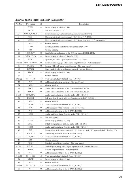
• DIGITAL BOARD IC1601 CXD9616R (AUDIO DSP2)<br />
<strong>STR</strong>-<strong>DB870</strong>/<strong>DB1070</strong><br />
Pin No. Pin Name I/O Description<br />
1 VDDI — Power supply terminal (+2.5V)<br />
2 EXTIN I Not used (fixed at “L”)<br />
3, 4 WMD1, WMD0 I External memory wait mode setting terminal (fixed at “H”)<br />
5 MOD1 I Mode select signal input terminal “L”: 384fs, “H”: 256fs<br />
6 MOD0 I Mode select signal input terminal “L”: single chip mode, “H”: can not use<br />
7 VSS — Ground terminal<br />
8 XRST I Reset signal input from the system controller (IC1703)<br />
9 VSS — Ground terminal<br />
10 SCKOUT O Serial clock signal output to the D/A converter (IC1201, 1202)<br />
11 VDDI (PLL) — Power supply terminal (+2.5V) (for PLL)<br />
12 SYNC I Sync/unsync select signal input terminal “L”: sync<br />
13 to 15 PAGE2 to PAGE0 O External memory page select signal output terminal Not used (open)<br />
16 PLOCK O Internal PLL lock signal output teminal Not used (open)<br />
17 BTACK I Boot mode display signal output teminal Not used (open)<br />
18 VDDE — Power supply terminal (+3.3V)<br />
19 VSS — Ground terminal<br />
20 to 22 D31 to D29 I/O Two-way data bus with the S-RAM (IC1602)<br />
23 A17 O Address signal output terminal Not used (open)<br />
24 VSS — Ground terminal<br />
25 SDO3 O Audio serial data output to the D/A converter (IC1201)<br />
26 SDO4 O Audio serial data output to the D/A converter (IC1202)<br />
27, 28 SDI1, SDI2 I Audio serial data input from the audio DSP1 (IC1501)<br />
29 LRCKI1 I L/R sampling clock signal input from the audio DSP1 (IC1501)<br />
30 VSS — Ground terminal<br />
31, 32 D28, D27 I/O Two-way data bus with the S-RAM (IC1602)<br />
33 A16 O Address signal output terminal Not used (open)<br />
34 A15 O Address signal output to the S-RAM (IC1602)<br />
35 SDI3 I Audio serial date input from the audio DSP1 (IC1501)<br />
36 L2 — Not used (open)<br />
37 VDDI — Power supply terminal (+2.5V)<br />
38 BCKI1 I Bit clock signal input from the audio DSP1 (IC1501)<br />
39 SDI4 I Audio serial data input from the audio DSP1 (IC1501)<br />
40 MS I Master/slave active select terminal “L”: internal clock, “H”: external clock (fixed at “L”)<br />
41, 42 A14, A13 O Address signal output to the S-RAM (IC1602)<br />
43, 44 D26, D25 I/O Two-way data bus with the S-RAM (IC1602)<br />
45 VSS — Ground terminal<br />
46 BCKI2 I Bit clock signal input terminal Not used (open)<br />
47, 48 FS2, FS1 I Sampling frequency select signal input terminal Not used (open)<br />
49 SPDIF I S/PDIF output terminal Not used (open)<br />
50 A12 O Address signal output to the S-RAM (IC1602)<br />
51 to 53 D24 to D22 I/O Two-way data bus with the S-RAM (IC1602)<br />
54 VDDE — Power supply terminal (+3.3V)<br />
55 VSS — Ground terminal<br />
56 to 58 D21 to D19 I/O Two-way data bus with the S-RAM (IC1602)<br />
59 A11 O Address signal output to the S-RAM (IC1602)<br />
47