
You also want an ePaper? Increase the reach of your titles
YUMPU automatically turns print PDFs into web optimized ePapers that Google loves.
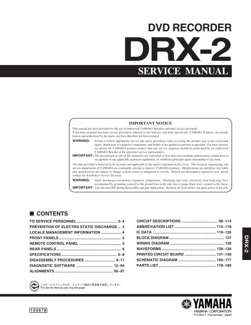
■ CONTENTS<br />
TO SERVICE PERSONNEL ...................................... 2~4<br />
PREVENTION OF ELECTRO STATIC DISCHARGE ... 4<br />
LOCALE MANAGEMENT INFORMATION ................... 4<br />
FRONT PANELS ............................................................ 5<br />
REMOTE CONTROL PANEL ........................................ 5<br />
REAR PANELS .............................................................. 6<br />
SPECIFICATIONS...................................................... 6~8<br />
DISASSEMBLY PROCEDURES ............................. 9~11<br />
DIAGNOSTIC SOFTWARE ................................... 12~94<br />
ALIGNMENTS ........................................................ 95~97<br />
100878<br />
DRX-2<br />
DVD RECORDER<br />
DRX-2<br />
SERVICE MANUAL<br />
IMPORTANT NOTICE<br />
This <strong>manual</strong> has been provided for the use of authorized YAMAHA Retailers and their <strong>service</strong> personnel.<br />
It has been assumed that basic <strong>service</strong> procedures inherent to the industry, and more specifically YAMAHA Products, are already<br />
known and understood by the users, and have therefore not been restated.<br />
WARNING: Failure to follow appropriate <strong>service</strong> and safety procedures when servicing this product may result in personal<br />
injury, destruction of expensive components, and failure of the product to perform as specified. For these reasons,<br />
we advise all YAMAHA product owners that any <strong>service</strong> required should be performed by an authorized<br />
YAMAHA Retailer or the appointed <strong>service</strong> representative.<br />
IMPORTANT: The presentation or sale of this <strong>manual</strong> to any individual or firm does not constitute authorization, certification or<br />
recognition of any applicable technical capabilities, or establish a principle-agent relationship of any form.<br />
The data provided is believed to be accurate and applicable to the unit(s) indicated on the cover. The research, engineering, and<br />
<strong>service</strong> departments of YAMAHA are continually striving to improve YAMAHA products. Modifications are, therefore, inevitable<br />
and specifications are subject to change without notice or obligation to retrofit. Should any discrepancy appear to exist, please<br />
contact the distributor's Service Division.<br />
WARNING: Static discharges can destroy expensive components. Discharge any static electricity your body may have<br />
accumulated by grounding yourself to the ground buss in the unit (heavy gauge black wires connect to this buss).<br />
IMPORTANT: Turn the unit OFF during disassembly and part replacement. Recheck all work before you apply power to the unit.<br />
CIRCUIT DESCRIPTIONS ................................... 98~114<br />
ABBREVIATION LIST ....................................... 115~118<br />
IC DATA ............................................................. 119~126<br />
BLOCK DIAGRAM ..................................................... 127<br />
WIRING DIAGRAM .................................................... 128<br />
WAVEFORMS .................................................... 129~130<br />
PRINTED CIRCUIT BOARD .............................. 131~149<br />
SCHEMATIC DIAGRAM .................................... 150~177<br />
PARTS LIST ....................................................... 178~189<br />
P.O.Box 1, Hamamatsu, Japan<br />
1<br />
DRX-2
DRX-2<br />
2<br />
DRX-2<br />
■ TO SERVICE PERSONNEL<br />
1. Critical Components Information<br />
Components having special characteristics are marked s<br />
and must be replaced with parts having specifications equal<br />
to those originally installed.<br />
2. Leakage Current Measurement (For 120V Models Only)<br />
When <strong>service</strong> has been completed, it is imperative to verify<br />
that all exposed conductive surfaces are properly insulated<br />
from supply circuits.<br />
● Meter impedance should be equivalent to 1500 ohm shunted<br />
by 0.15µF.<br />
WALL<br />
OUTLET<br />
WARNING: CHEMICAL CONTENT NOTICE!<br />
EQUIPMENT<br />
UNDER TEST<br />
INSULATING<br />
TABLE<br />
● Leakage current must not exceed 0.5mA.<br />
AC LEAKAGE<br />
TESTER OR<br />
EQUIVALENT<br />
● Be sure to test for leakage with the AC plug in both polarities.<br />
THE DVD RECORDER SHOULD NOT BE ADJUSTED OR REPAIRED BY ANYONE EXCEPT PROPERLY QUALIFIED<br />
SERVICE PERSONNEL.<br />
CAUTION<br />
1001 (ANALOG P.C.B.): FOR CONTINUED PROTECTION AGAINST RISK OF FIRE, REPLACE ONLY WITH SAME TYPE 125mA, 250V FUSE.<br />
1300 (ANALOG P.C.B.): FOR CONTINUED PROTECTION AGAINST RISK OF FIRE, REPLACE ONLY WITH SAME TYPE 2.5A, 250V FUSE.<br />
1303 (ANALOG P.C.B.): FOR CONTINUED PROTECTION AGAINST RISK OF FIRE, REPLACE ONLY WITH SAME TYPE 1.0A, 250V FUSE.<br />
1304 (ANALOG P.C.B.): FOR CONTINUED PROTECTION AGAINST RISK OF FIRE, REPLACE ONLY WITH SAME TYPE 4.0A, 250V FUSE.<br />
1306 (ANALOG P.C.B.): FOR CONTINUED PROTECTION AGAINST RISK OF FIRE, REPLACE ONLY WITH SAME TYPE 125mA, 250V FUSE.<br />
1307 (ANALOG P.C.B.): FOR CONTINUED PROTECTION AGAINST RISK OF FIRE, REPLACE ONLY WITH SAME TYPE 1.0A, 250V FUSE.<br />
1308 (ANALOG P.C.B.): FOR CONTINUED PROTECTION AGAINST RISK OF FIRE, REPLACE ONLY WITH SAME TYPE 500mA, 250V FUSE.<br />
1309 (ANALOG P.C.B.): FOR CONTINUED PROTECTION AGAINST RISK OF FIRE, REPLACE ONLY WITH SAME TYPE 800mA, 250V FUSE.<br />
1505 (DIGITAL P.C.B.): FOR CONTINUED PROTECTION AGAINST RISK OF FIRE, REPLACE ONLY WITH SAME TYPE 1.0A, 125V FUSE.<br />
1506 (DIGITAL P.C.B.): FOR CONTINUED PROTECTION AGAINST RISK OF FIRE, REPLACE ONLY WITH SAME TYPE 1.0A, 125V FUSE.<br />
1507 (DIGITAL P.C.B.): FOR CONTINUED PROTECTION AGAINST RISK OF FIRE, REPLACE ONLY WITH SAME TYPE 1.0A, 125V FUSE.<br />
CAUTION<br />
1001 (ANALOG P.C.B.): REPLACE WITH SAME TYPE 125mA, 250V FUSE.<br />
1300 (ANALOG P.C.B.): REPLACE WITH SAME TYPE 2.5A, 250V FUSE.<br />
1303 (ANALOG P.C.B.): REPLACE WITH SAME TYPE 1.0A, 250V FUSE.<br />
1304 (ANALOG P.C.B.): REPLACE WITH SAME TYPE 4.0A, 250V FUSE.<br />
1306 (ANALOG P.C.B.): REPLACE WITH SAME TYPE 125mA, 250V FUSE.<br />
1307 (ANALOG P.C.B.): REPLACE WITH SAME TYPE 1.0A, 250V FUSE.<br />
1308 (ANALOG P.C.B.): REPLACE WITH SAME TYPE 500mA, 250V FUSE.<br />
1309 (ANALOG P.C.B.): REPLACE WITH SAME TYPE 800mA, 250V FUSE.<br />
1505 (DIGITAL P.C.B.): REPLACE WITH SAME TYPE 1.0A, 125V FUSE.<br />
1506 (DIGITAL P.C.B.): REPLACE WITH SAME TYPE 1.0A, 125V FUSE.<br />
1507 (DIGITAL P.C.B.): REPLACE WITH SAME TYPE 1.0A, 125V FUSE.<br />
ATTENTION<br />
1001 (ANALOG P.C.B.): UTILISER UN FUSIBLE DE RECHANGE DE MEME TYPE DE 125mA, 250V.<br />
1300 (ANALOG P.C.B.): UTILISER UN FUSIBLE DE RECHANGE DE MEME TYPE DE 2.5A, 250V.<br />
1303 (ANALOG P.C.B.): UTILISER UN FUSIBLE DE RECHANGE DE MEME TYPE DE 1.0A, 250V.<br />
1304 (ANALOG P.C.B.): UTILISER UN FUSIBLE DE RECHANGE DE MEME TYPE DE 4.0A, 250V.<br />
1306 (ANALOG P.C.B.): UTILISER UN FUSIBLE DE RECHANGE DE MEME TYPE DE 125mA, 250V.<br />
1307 (ANALOG P.C.B.): UTILISER UN FUSIBLE DE RECHANGE DE MEME TYPE DE 1.0A, 250V.<br />
1308 (ANALOG P.C.B.): UTILISER UN FUSIBLE DE RECHANGE DE MEME TYPE DE 500mA, 250V.<br />
1309 (ANALOG P.C.B.): UTILISER UN FUSIBLE DE RECHANGE DE MEME TYPE DE 800mA, 250V.<br />
1505 (DIGITAL P.C.B.): UTILISER UN FUSIBLE DE RECHANGE DE MEME TYPE DE 1.0A, 125V.<br />
1506 (DIGITAL P.C.B.): UTILISER UN FUSIBLE DE RECHANGE DE MEME TYPE DE 1.0A, 125V.<br />
1507 (DIGITAL P.C.B.): UTILISER UN FUSIBLE DE RECHANGE DE MEME TYPE DE 1.0A, 125V.<br />
The solder used in the production of this product contains LEAD. In addition, other electrical/electronic and /or plastic<br />
(where applicable) components may also contain traces of chemicals found by the California Health and Welfare Agency<br />
(and possibly other entities) to cause cancer and/or birth defects or other reproductive harm.<br />
DO NOT PLACE SOLDER, ELECTRICAL/ELECTRONIC OR PLASTIC COMPONENTS IN YOUR MOUTH FOR ANY REA-<br />
SON WHATSOEVER!<br />
Avoid prolonged, unprotected contact between solder and your skin! When soldering, do not inhale solder fumes or expose<br />
eyes to solder/flux vapor!<br />
If you come in contact with solder or components located inside the enclosure of this product, wash your hands before<br />
handling food.
WARNING: Laser Safety<br />
DRX-2<br />
This product contains a laser beam component. This component may emit invisible, as well as visible radiation, which may<br />
cause eye damage. To protect your eyes and skin from laser radiation, the following precautions must be used during<br />
servicing of the unit.<br />
1) When testing and/or repairing any component within the product, keep your eyes and skin more than 30 cm away from<br />
the laser pick-up unit at all times. Do not stare at the laser beam at any time.<br />
2) Do not attempt to readjust, disassemble or repair the laser pick-up, unless noted elsewhere in this <strong>manual</strong>.<br />
3) CAUTION: Use of controls, adjustments or performance of procedures other than those specified herein may result in<br />
hazardous radiation exposure.<br />
Laser Emitting conditions:<br />
1) When the Top Cover is removed and the "STANDBY/ON" SW is turned to the "ON" position, the laser component will emit<br />
a beam for several seconds to detect if a disc is present. During this time (5 - 10 sec.) the laser may radiate through the<br />
lens of the laser pick-up unit. Do not attempt any servicing during this period!<br />
If no disc is detected, the laser will stop emitting the beam. When a disc is loaded, you will not be exposed to any laser<br />
emissions.<br />
2) The laser power level can be adjusted with the VR on the pick-up PWB. However, this level has been set by the factory prior to<br />
shipping from the factory. Do not adjust this laser level control unless instruction is provided elsewhere in this <strong>manual</strong>.<br />
Adjustment of this control can increase the laser emission level from the device.<br />
Laser Diode Properties<br />
Type: InGaAIP Semiconductor laser (DVD)<br />
AlGaAs Semiconductor laser (CD)<br />
Wave length: 660 nm (DVD)<br />
780 nm (CD)<br />
Output Power: 20 mW (DVD writing)<br />
(out of objective) 0.8 mW (DVD reading)<br />
0.3mW (CD reading)<br />
Beam divergence: 82 degrees (DVD)<br />
54 degrees (CD)<br />
VARO! : AVATTAESSA JA SUOJALUKITUS OHITETTAESSA OLET ALTTIINA NÄkymÄTTÖMÄLLE LASER-<br />
SÄTEILYLLE. ÄLÄ KATSO SÄTEESEEN.<br />
VARNING! : OSYNLIG LASERSTRÅLNING NÄR DENNA DEL ÄR ÖPPNAD OCH SPÄRREN ÄR URKOPPLAD.<br />
BETRAKTA EJ STRÅLEN.<br />
WARNING<br />
The use of optical instruments with this product will<br />
increase eye hazard.<br />
Repair handling should take place as much as possible<br />
with a disc loaded inside the player.<br />
CAUTION: Visible and invisible laser radiation<br />
when open. Avoid exposure to beam.<br />
CLASS 1<br />
LASER PRODUCT<br />
CAUTION: Visible and invisible laserradiation<br />
when open. Avoid exposure to beam.<br />
WARNING LOCATION: Top of the DVDR Mechanism<br />
3<br />
DRX-2
DRX-2<br />
4<br />
DRX-2<br />
Warning for power supply<br />
The primary side of the power supply carries live mains voltage when the player is connected to the mains even<br />
when the player is switched off !<br />
This primary area is not shielded so it is possible to touch copper tracks and/or components when servicing the player.<br />
Service personnel have to take precautions to prevent touching this area or components in this area .<br />
The primary side of the power supply has been indicated with a lightening stroke and a stripe-marked print on the printed<br />
wiring board<br />
Note:<br />
The screws on the DVDR mechanism may never be touched, removed or re-adjusted.<br />
Handle the DVDR mechanism with care when the unit has to be exchanged!<br />
The DVDR mechanism is very sensitive for dropping or giving shocks.<br />
■ PREVENTION OF ELECTRO STATIC DISCHARGE<br />
The laser diode in the DVDR mechanism may be damaged due to static electricity from clothes or the human body. Use<br />
caution to prevent electrostatic damage when servicing or handling the DVDR mechanism.<br />
1. Grounding for electrostatic damage prevention<br />
Some devices, such as the DVD <strong>recorder</strong>, use an optical pickup (laser diode) that will be damaged by static electricity in the<br />
working environment. Only attempt <strong>service</strong> after ensuring that all grounding procedures have been completed.<br />
1. Worktable grounding<br />
Put a grounded conductive material (sheet) or iron sheet on the area where the optical pickup is placed.<br />
2. Human body grounding<br />
Use an anti-static wrist strap to discharge the static electricity from your body.<br />
Anti-static wrist strap<br />
2. Handling Precautions for DVDR mechanism<br />
■ LOCALE MANAGEMENT INFORMATION<br />
1M<br />
Locale Management Information : This DVD <strong>recorder</strong> is designed and manufactured to respond to the Locale Management<br />
Information that is recorded on the DVDR disc. If the Locale number described on the DVDR disc does not correspond to the<br />
Locale number of this DVD <strong>recorder</strong>, this DVD <strong>recorder</strong> cannot play this disc.<br />
This product incorporates copyright protection<br />
technology that is protected by method claims of<br />
certain U.S. patents and other intellectual<br />
property rights owned by Macrovision<br />
Corporation and other rights owners. Use of this<br />
copyright protection technology must be<br />
authorized by Macrovision Corporation, and is<br />
intended for home and other limited viewing uses<br />
only unless otherwise authorized by Macrovision<br />
Corporation. Reverse engineering or<br />
disassembly is prohibited.<br />
1<br />
4<br />
2<br />
Conductive material<br />
(sheet) or iron sheet<br />
1. Handle the DVDR mechanism gently, as it is an extremely high-precision assembly.<br />
2. The flexible cable lines may break if an excessive force is applied to it. Use caution when handling the cable.<br />
3. The semi-fixed resistor for laser power adjustment should not be adjusted. Do not turn the resistor.<br />
2<br />
5<br />
5<br />
6<br />
5<br />
3<br />
4<br />
2
■ FRONT PANELS<br />
U model<br />
A model<br />
G model<br />
NATURAL SOUND DVD RECORDER DRX-2<br />
■ REMOTE CONTROL PANEL<br />
S VIDEO VIDEO L AUDIO R DV IN<br />
CAM 1 CAM 2<br />
DRX-2<br />
5<br />
DRX-2
DRX-2<br />
6<br />
DRX-2<br />
■ REAR PANELS<br />
U model<br />
A model<br />
G model<br />
■ SPECIFICATIONS<br />
DISC FORMATS SUPPORTED<br />
Disc type Playback Recording<br />
DVD+RW • •<br />
DVD+R • •<br />
DVD-RW (Video mode) • —<br />
DVD-R • —<br />
DVD-Video • —<br />
SVCD • —<br />
Video CD • —<br />
Audio CD • —<br />
CD-R • —<br />
CD-RW • —<br />
Apparatus Claims of U.S. Patent Nos.<br />
4.631.603, 4.577.216, 4.819.098, 4.907.093<br />
6.466.734, 6.430.359, 6.091.882,<br />
6.049.652, 5.335.079, 5.307.173<br />
licensed for limited viewing uses only.<br />
RECORDABLE DISC FORMATS<br />
Medium DVD+RW: Phase-Change ReWritable<br />
DVD+R: dye-based<br />
Diameter 12 cm<br />
Capacity (single side) 4.7 Gbyte<br />
Recording time M1 60’ 9.72 Mbit/s<br />
M2 120’ 5.07 Mbit/s<br />
M2x 150’ 4.06 Mbit/s<br />
M3 180’ 3.38 Mbit/s<br />
M4 240’ 2.54 Mbit/s<br />
M6 360' 1.69 Mbit/s
TV Standard PAL NTSC<br />
Scan Frequency 50Hz 60Hz<br />
Number of Lines 625 525<br />
Playback • •<br />
Recording • •<br />
Internal Tuner • –<br />
VIDEO RESOLUTION 50Hz 60Hz<br />
DVD-Video/DVD+RW/DVD+R(M1/M2/M2x)<br />
• Horiz. Resolution 720 pixels1 720 pixels1 • Vertical Resolution 576 lines 480 lines<br />
DVD+RW_DVD+R(M3/M4/M6)<br />
• Horiz. Resolution 360 pixels2 360 pixels2 • Vertical Resolution<br />
VCD<br />
576 lines 480 lines<br />
• Horiz. Resolution 352 pixels 352 pixels<br />
• Vertical Resolution 288 lines 288 lines<br />
1 equivalent to 500 lines on your TV<br />
2 equivalent to 250 lines on your TV<br />
VIDEO PERFORMANCE<br />
DA Converter 10-bit<br />
AD Converter 9-bit<br />
Signal Handling Components<br />
Video Output 1 Vpp into 75 ohms<br />
S-video Output Y: 1 Vpp into 75 ohms<br />
C: 0.286 Vpp into 75 ohms (U, A models)<br />
C: 0.300 Vpp into 75 ohms (G model)<br />
Component Output Y: 1Vpp into 75 ohms (U, A models)<br />
Pb: 0.7 Vpp into 75 ohms (U, A models)<br />
Pr: 0.7 Vpp into 75 ohms (U, A models)<br />
RGB Output 0.7 Vpp into 75 ohms (G model)<br />
AUDIO FORMAT<br />
Compressed Digital Playback Recording<br />
• Dolby Digital Multi-channel 2-channel<br />
(AC-3) 16 bit, fs 48 kHz<br />
• DTS Multi-channel —<br />
• MPEG1 2-channel<br />
SPdif<br />
—<br />
• PCM 2-channel 2-channel<br />
16, 20, 24 bit<br />
fs 48 kHz<br />
16 bit, fs 48 kHz<br />
AUDIO PERFORMANCE<br />
DA Converter 24-bit<br />
AD Converter 16-bit<br />
DVD fs 96 kHz 4 Hz - 44 kHz<br />
fs 48 kHz 4 Hz - 22 kHz<br />
Video CD fs 44.1 kHz 4 Hz - 20 kHz<br />
Audio CD fs 44.1 kHz 4 Hz - 20 kHz<br />
FRONT CONNECTIONS<br />
i.LINK DV IEEE 1394 4-pin<br />
S-video Input Hosiden 4-pin<br />
Video Input Cinch (yellow)<br />
Audio Left/Right Input Cinch (white/red)<br />
DRX-2<br />
REAR CONNECTIONS<br />
Component Video Input Cinch (green/blue/red)<br />
Component Video Output Cinch (green/blue/red)<br />
S-video Input Hosiden 4-pin (U, A models)<br />
S-video Output Hosiden 4-pin<br />
Video Input Cinch (yellow) (U, A model)<br />
Video Output Cinch (yellow)<br />
scart 1 CVBS, S-video/RGB-out, Decoder (G model)<br />
scart 2 CVBS, S-video/RGB-in, Decoder (G model)<br />
Audio L/R Input Cinch (white/red) (U, A models)<br />
Audio L/R Output Cinch (white/red)<br />
Digital Audio Output 1 coaxial, 1 optical<br />
IEC958 for CDDA / LPCM<br />
IEC1937 for MPEG2, Dolby Digital (U, A models)<br />
IEC1937, Dolby Digital, DTS (G model)<br />
RF Antenna Input Coaxial 75 ohms<br />
RF TV Output Coaxial 75 ohms<br />
Power Standard (IEC type)<br />
POWER SUPPLY<br />
Power Supply<br />
U model 120V, 60Hz<br />
A, G models 220 - 240V, 50 Hz<br />
Power Consumption Operation 27 W<br />
Low-power standby 3 W<br />
CABINET<br />
Dimensions (WxHxD) 435 x 82 x 347 mm (17-1/8" x 3-1/4" x 13-11/16")<br />
Net Weight 4.0 kg (8 lbs. 13 oz.)<br />
OPERATING ENVIRONMENT<br />
Operating Position maximum 10 degree inclination in all directions<br />
Ambient Temperature 15 – 35 °C (59 – 95 °F)<br />
Humidity 25 – 75 %<br />
ACCESSORIES<br />
- Remote Control x 1<br />
- Battery x 2<br />
- Power Cable x 1<br />
- SCART Cable x 1 (G model)<br />
- Audio Pin Cable (2P) x 1 (U, A models)<br />
- Video Cable (1P) x 1 (U, A models)<br />
- RF Cable for NAFTA x 1 (U model)<br />
- RF Cable for PAL x 1 (A, G models)<br />
- Pin Cable (3P) x 1 (U, A models)<br />
- DVD+RW Disc x 1 (U, A models)<br />
* Specifications are subject to change without notice due<br />
to product improvements.<br />
U ........ U.S.A. model A ........ Australian model<br />
G ........ European model<br />
7<br />
DRX-2
DRX-2<br />
8<br />
DRX-2<br />
Simple programming system for DVD<br />
<strong>recorder</strong>s. Simply enter the number<br />
code associated with your television<br />
program. This number is located in your<br />
television listings magazine.<br />
Manufactured under license from Dolby Laboratories.<br />
“Dolby”, “Pro Logic” and the double-D symbol are trademarks<br />
of Dolby Laboratories. Confidential Unpublished Works.<br />
©1992 1997 Dolby Laboratories,Inc. All rights reserved.<br />
“DTS” and “DTS Digital Out” are trademarks of Digital Theater<br />
Systems, Inc.<br />
This product incorporates copyright protection technology<br />
that is protected by method claims of certain U.S.patents and<br />
other intellectual property rights owned by Macrovision<br />
Corporation and other rights owners.<br />
Use of this copyright protection technology must be<br />
authorized by Macrovision Corporation, and is intended for<br />
home and other limited viewing uses only unless otherwise<br />
authorized by Macrovision Corporation. Reverse engineering<br />
or dis-assembly is prohibited.
■ DISASSEMBLY PROCEDURES<br />
See exploded view for item numbers mounting<br />
demounting<br />
Cover 300<br />
⇒ Remove 9 screws 200<br />
⇒ Lift the cover to remove<br />
DVDR MECHANISM 1007<br />
⇒ Remove the connections<br />
⇒ Open the tray and remove the tray lid 70<br />
⇒ Remove 4 screws 202<br />
(DVDR Mechanism 1007 → support<br />
bracket)<br />
⇒ Demount the DVDR Mechanism<br />
Digital Board 1002<br />
⇒ Remove the connections<br />
⇒ Remove 4 screws 201<br />
(Digital board → frame)<br />
⇒ Demount the board<br />
IOE Board 1005<br />
⇒ Remove 2 screws 202 and screw 201<br />
(IOE board → rear panel)<br />
⇒ Demount the board<br />
Front Panel Unit<br />
⇒ Open the tray and remove the<br />
tray lid 70<br />
⇒ Remove 3 screws 201<br />
(front panel unit → frame)<br />
⇒ Unlock the front panel unit<br />
from the frame by releasing 2<br />
snaps on left and right<br />
⇒ Remove 8 screws 205 to<br />
remove the plate front<br />
Manual opening of tray and removal of<br />
tray lid 70<br />
In case the loader is defective and cannot<br />
be opened electrically, you can open the<br />
tray as follows:<br />
Analog Board 1001<br />
⇒ Remove the connections<br />
⇒ Remove 2 screws 201<br />
and 7 (U, A models) or 3<br />
(G model) screws 202<br />
(board → rear panel)<br />
⇒ Remove 3 screws 201<br />
and screw 200<br />
(board → frame)<br />
⇒ Remove screw safety<br />
holder 145<br />
⇒ Demount the board<br />
Display Board 1004<br />
⇒ Remove 2 screws 205<br />
(board → front panel ass'y 1)<br />
⇒ Remove 2 screws 209 of DV<br />
input cable<br />
⇒ Demount the board<br />
⇒ It is possible to unlock the tray by means<br />
of a screwdriver via a slot in the front and<br />
frame at the underside.<br />
Push the white pin of the slider at the<br />
underside of the DVDR Mechanism to the<br />
right (seen from the front)<br />
⇒ Open the unlocked tray.<br />
When disassembling, use the special screw driver with<br />
tip shape in figure.<br />
2.7 mm<br />
T10<br />
Fr Front Front ont Panel PPanel<br />
anel<br />
2.2 mm<br />
T8<br />
DRX-2<br />
9<br />
DRX-2
DRX-2<br />
10<br />
DRX-2<br />
● Dismantling and Assembly of the Set<br />
For item numbers please see the exploded views.<br />
1. Front<br />
a. After removing the top cover, remove tray lid 70. (Fig. 1)<br />
b. Remove the 3 screws 201. (Fig. 2)<br />
c. Release the 2 snap hooks on the sides and remove the<br />
front panel unit. (Fig. 2)<br />
d. Remove the 8 screws 205 to remove the front plate.<br />
(Fig. 3 and 4)<br />
Fig. 1<br />
3 2 3<br />
2 2<br />
4<br />
Fig. 2<br />
Fig. 3<br />
6<br />
Fig. 4<br />
1<br />
5<br />
2. Digital Board<br />
a. Remove the 4 screws 201. (Fig. 5)<br />
b. Turn the PCB in the <strong>service</strong> position. (Fig. 6)<br />
1 1<br />
1<br />
Fig. 5<br />
2<br />
Fig. 6<br />
1
3. DVDR Mechanism<br />
a. Remove the 4 screws 202. (Fig. 7)<br />
b. Turn the DVDR mechanism in the <strong>service</strong> position. (Fig. 8)<br />
1 1<br />
1<br />
Fig. 7<br />
2<br />
Fig. 8<br />
1<br />
DRX-2<br />
4. Analog Board<br />
a. Remove the 7 screws 200 and 201. (Fig. 9)<br />
b. Remove screw safety holder 145. (Fig. 9)<br />
c. Unlock the 2 snaps hooks on the left and right. (Fig. 10)<br />
d. Turn the PCB in the <strong>service</strong> position. (Fig. 11)<br />
2<br />
1<br />
1<br />
1<br />
1<br />
1 1 1<br />
Fig. 9<br />
(U, A models)<br />
3 3<br />
Fig. 10<br />
4<br />
Fig. 11<br />
(U, A models)<br />
(U, A models)<br />
11<br />
DRX-2
DRX-2<br />
12<br />
DRX-2<br />
■ DIAGNOSTIC SOFTWARE<br />
Due to the complexity of the DVD <strong>recorder</strong>, the time to find<br />
a defect in the <strong>recorder</strong> can become long. To reduce this<br />
time, the <strong>recorder</strong> has been equipped with Diagnostic and<br />
Service software (DS). The DS offers functionality to<br />
diagnose the DVDR hardware and tests the following:<br />
• Interconnections between components<br />
• Accessibility of components<br />
• Functionality of the audio and video paths<br />
This functionality can be accessed via several interfaces:<br />
1. End user/Dealer script interface<br />
2. Player script interface<br />
1. End User/Dealer Script Interface<br />
1.1 Description<br />
The End user/Dealer script interface gives a diagnosis on<br />
a stand alone DVD <strong>recorder</strong>; no other equipment is<br />
needed. During this mode, a number of hardware tests<br />
(nuclei) are automatically executed to check if the <strong>recorder</strong><br />
is faulty. The diagnosis is simply a "fail" or "pass"<br />
message. If the message "FAIL" appears on the display,<br />
there is apparently a failure in the <strong>recorder</strong>. If the message<br />
"PASS" appears, the nuclei in this mode have been<br />
executed successfully. There can be still a failure in the<br />
<strong>recorder</strong> because the nuclei in this mode don't cover the<br />
complete functionality of the <strong>recorder</strong>.<br />
1.3 Contents for sets with Digital Board Chrysalis<br />
1.2 Contents<br />
Unplug the power cord<br />
Hold key pressed<br />
while you plug the <strong>recorder</strong><br />
During the test, the following display<br />
is shown: the counter counts down<br />
from the number of nuclei to be run<br />
before the test finishes. Example:<br />
SET O.K.?<br />
Included tests: 1. DS_ANAB_COMMUNICATIONECHO_NUC<br />
2. DS_DCB_COMMUNICATIONECHO_NUC<br />
3. DS_BROM_COMMUNICATION_NUC<br />
4. DS_SYS_SETTINGSDISPLAY_NUC<br />
5. DS_CHR_DEVTYPEGET_NUC<br />
6. DS_CHR_INT_PIC_NUC<br />
7. DS_CHR_DMA_NUC<br />
8. DS_BROM_WRITEREAD_NUC<br />
9. DS_NVRAM_COMMUNICATION_NUC<br />
10. DS_NVRAM_WRITEREAD_NUC<br />
11. DS_SDRAM_WRITEREADFAST_NUC<br />
12. DS_FLASH_WRITEREAD_NUC<br />
13. DS_FLASH_CHECKSUMPROGRAM_NUC<br />
14. DS_SYS_HARDWAREVERSIONGET_NUC<br />
15. DS_VIP_DEVTYPEGET_NUC<br />
16. DS_VIP_COMMUNICATION_NUC<br />
17. DS_DVIO_LINKDEVTYPEGET_NUC<br />
18. DS_DVIO_PHYDEVTYPEGET_NUC<br />
19. DS_DVIO_LINKCOMMUNICATION_NUC<br />
20. DS_DVIO_PHYCOMMUNICATION_NUC<br />
21. DS_PSCAN_COMMUNICATIONDENC_NUC<br />
22. DS_PSCAN_COMMUNICATIONDEINTERLACER_NUC<br />
23. DS_BE_COMMUNICATIONECHO_NUC<br />
24. DS_ANAB_COMMUNICATIONIICNVRAM_NUC<br />
25. DS_ANAB_COMMUNICATIONIICTUNER_NUC<br />
26. DS_ANAB_COMMUNICATIONIICSOUNDPROCESSOR_NUC<br />
27. DS_ANAB_COMMUNICATIONIICAVSELECTOR_NUC<br />
28. DS_ANAB_CHECKSUMPROGRAM_NUC<br />
YES<br />
NO<br />
To exit DEALER SCRIPT, unplug the power cord<br />
Fig. A<br />
The End use/Dealer script executes all diagnostic nuclei<br />
that do not need any user interaction and are meaningful<br />
on a standalone DVD <strong>recorder</strong>.
1.4 Error Log<br />
Explanation:<br />
The application errors will be logged in the NVRAM. The<br />
maximum number of error bytes that will be visible is 19.<br />
The last reported error is shown as DN D0000000, the<br />
oldest visible error as D0000000 UP and the errors in<br />
between as DN D0000000 UP. DN stands for DOWN, UP<br />
stands for UPWARDS. The shown error codes are<br />
identical to the Nuclei Error Codes (paragraph 3).<br />
1.5 Trade Mode<br />
TRADE MODE<br />
When the <strong>recorder</strong> is in Trade Mode, the <strong>recorder</strong><br />
cannot becontrolled by means of the front key<br />
buttons, but only by means of the remote control.<br />
IF TRADE MODE OFF<br />
UNPLUG THE RECORDER<br />
PRESS 2 KEYS<br />
SIMULTANEOUSLY<br />
+ <br />
PLUG THE RECORDER<br />
RECORDER IS IN TRADE MODE<br />
WHEN PRESSING FRONT<br />
KEYS, THE RECORDER<br />
DOESN'T RESPOND<br />
Fig. B<br />
IF TRADE MODE ON<br />
UNPLUG THE RECORDER<br />
PRESS 2 KEYS<br />
SIMULTANEOUSLY<br />
+ <br />
PLUG THE RECORDER<br />
RECORDER IS IN NORMAL MODE<br />
WHEN PRESSING FRONT<br />
KEYS, THE RECORDER<br />
WILL RESPOND<br />
1.6 Virgin mode<br />
If you want that the <strong>recorder</strong> starts up in Virgin mode,<br />
follow this procedure:<br />
• Unplug the <strong>recorder</strong><br />
• plug the <strong>recorder</strong> again while you keep the STANDBY/<br />
ON key pressed<br />
• the set starts up in Virgin mode.<br />
2. Menu and Command Mode Interface<br />
DRX-2<br />
2.1 Nuclei Numeration<br />
Each nucleus has a unique number of four digits. This<br />
number is the input of the command mode.<br />
[ XX YY ]<br />
Nucleus number<br />
Nucleus group number<br />
Fig. 1<br />
The following groups are defined for Digital Board 1.5,<br />
Empress:<br />
Group number Group name<br />
0 Basic / Scripts<br />
1 Host decoder (Sti5505 and memory)<br />
2 Audio / video encoder (DVDR only)<br />
3 VSM (DVDR only)<br />
4 NVRAM<br />
5 Front Panel<br />
6 DVDR Mechanism<br />
7 Analog board (DVDR only)<br />
8 DVIO (DVDR only)<br />
9 Loop nuclei (DVDR only)<br />
10 Library sub nuclei (I2C nuclei)<br />
11 User interface<br />
12 Furore (SACD only)<br />
13 DAC (SACD only)<br />
The following groups are defined for Digital Board<br />
Chrysalis:<br />
Group number Group name<br />
0 Basic/Scripts<br />
1 Chrysalis<br />
2 Boot EEPROM<br />
3 NVRAM<br />
4 SDRAM<br />
5 Flash<br />
6 Video Input Processor<br />
7 DVIO<br />
8 Progressive Scan<br />
9 DVDR Mechanism<br />
10 Display and Control Board<br />
11 Analog Board<br />
12 System<br />
13<br />
DRX-2
DRX-2<br />
14<br />
DRX-2<br />
2.2 Error Handling<br />
Each nucleus returns an error code. This code contains<br />
six numerals, which means:<br />
[ XX YY ZZ ]<br />
Error code<br />
Nucleus number<br />
Nucleus group number<br />
Fig. 2<br />
The nucleus group numbers and nucleus numbers are the<br />
same as above.<br />
2.3 Command Mode Interface<br />
Set-Up Physical Interface Components<br />
Hardware required:<br />
• Service PC<br />
• one free COM port on the Service PC<br />
• special cable to connect DVD <strong>recorder</strong> to Service PC<br />
The <strong>service</strong> PC must have a terminal emulation program<br />
(e.g. Hyperterminal) installed and must have a free COM<br />
port (e.g. COM1). Activate the terminal emulation program<br />
and check that the port settings for the free COM port are:<br />
19200 bps, 8 data bits, no parity, 1 stop bit and no flow<br />
control. The free COM port must be connected via a<br />
special cable to the RS232 port of the DVD <strong>recorder</strong>. This<br />
special cable will also connect the test pin, which is<br />
available on the connector, to ground (i.e. activate test<br />
pin).<br />
Code number of PC interface cable: 3122 785 90017<br />
(AAX57390)<br />
Activation Digital Board Chrysalis<br />
1. Pull the mains cord from the <strong>recorder</strong> and reconnect it<br />
again (reboot).<br />
2. The next welcome message will appear on the PC:<br />
Welcome screen D&S program<br />
Fig. 3<br />
Now, the prompt 'DS:>' will appear. The diagnostic<br />
software is now ready to receive commands. The<br />
commands that can be given are the numbers of the<br />
nuclei. If you see above shown screen, continue with<br />
paragraph 'Nuclei Codes'.<br />
3. It is possible that the next message will appear when<br />
starting the DVD+RW for the first time<br />
Error message D&S program<br />
Fig. 4<br />
In this case, the boot EEPROM of the Chrysalis Digital<br />
Board does not contain the required string with the<br />
hardware information. To update the Digital Board with the<br />
correct string, nucleus 1226 must be executed.<br />
Before doing so, one must generate this string. In order to<br />
generate the correct parameters, an MS Windows utility,<br />
called "dbstring.exe", is available (contact your Philips<br />
regional <strong>service</strong> support for this). For a detailed<br />
description, see next section 'String Generation'.<br />
String Generation<br />
4. Browse to the directory with the Diagnostics software<br />
(e.g. type 'cd c:\ds\'), and execute the 'dbstring.exe'<br />
application.<br />
Opening screen 'dbstring' program<br />
Fig. 5<br />
5. Type '1' for a list of DVD <strong>recorder</strong>s, or '2' for a list of<br />
Chrysalis Digital boards. In this example, '2' is entered.
Board overview<br />
Fig. 6<br />
6. You now are asked to enter an ID of the board that must<br />
be programmed. Type a number, e.g. '6' followed by<br />
'Enter'.<br />
Board periphery<br />
Fig. 7<br />
7. Confirm the choice by typing 'y' followed by 'Enter'. Now<br />
press any key to return to the prompt.<br />
8. A text file called 'DBSTRING.TXT' is created, which<br />
contains the parameters that are necessary for nucleus<br />
1226. Copy this string from the text-file (e.g. by using<br />
'Ctrl C').<br />
Example of the string<br />
Fig. 8<br />
DRX-2<br />
9. Execute nucleus 1226 with the string (paste with 'Edit'<br />
> 'Paste to host').<br />
Nucleus 1226 execution with string<br />
Fig. 9<br />
10. To check if the hardware info is filled correctly, you can<br />
execute nucleus 1228.<br />
Nucleus 1228 info example<br />
Fig. 10<br />
11. Exit the 'Terminal' program.<br />
12. Reboot the DVD <strong>recorder</strong> to allow the software to start.<br />
Browse to the directory with the Diagnostics software<br />
(e.g. type 'cd c:\ds\'), and execute the 'dbstring.exe'<br />
application.<br />
15<br />
DRX-2
DRX-2<br />
16<br />
DRX-2<br />
Command overview Digital Board Chrysalis<br />
Below you will find an overview of the nuclei, their<br />
numbers, and their error codes. This overview is<br />
preliminary and subject to modifications.<br />
Chrysalis (CHR)<br />
Nucleus Name DS_CHR_DevTypeGet<br />
Nucleus Number 100<br />
Description Sends the device ID and the module ids and revisions of the PNX7100 (Chrysalis) to the<br />
stdout port.<br />
Technical - Determine the codec ID by means of comparing version ids of the modules.<br />
- Read the module-id register from every module.<br />
Execution Time Less than 1 second.<br />
User Input None<br />
Error Number Description<br />
10000 Getting the information succeeded<br />
10001 Wrong codec ID detected<br />
Example DS:> 100<br />
Device ID 7100<br />
Codec ID PNX7100_MF2<br />
F-BCU (0x0102) 1.0 INTC (0x011d) 1.0 PCI-XIO(0x0113) 1.0<br />
SIF(0x013b) 1.0 EJTAG (0x0104) 0.0 S-BCU (0x0102) 1.0<br />
BOOT (0x010a) 1.0 CONFIG (0x013f) 1.0 RESET (0x0123) 1.0<br />
DEBUG (0x0116) 0.0 UART0 (0x0107) 0.1 UART1 (0x0107) 0.1<br />
UART2 (0x0107) 0.1 UART3 (0x0107) 0.1 I2C0 (0x0105) 0.1<br />
I2C1 (0x0105) 0.1 GPIO (0x013c) 1.0 SYNC (0x013a) 1.0<br />
DISP0 (0xa015) 0.1 DISP1 (0xa00f) 0.0 OSD (0x0136) 0.1<br />
SPU (0xa00e) 0.0 MIXER (0x0137) 1.0 DENC (0x0138) 0.1<br />
CCIR (0x0139) 1.0 VDEC (0x0133) 0.1 PARSER (0xa00d) 0.0<br />
DV (0xa00c) 0.0 BEI (0xa00a) 0.0 IDE (0xa009) 0.0<br />
SGDX (0xa008)0.0 BYTE (0xa00b) 0.0 OUTPUT (0xa003) 0.0<br />
ACOMP (0xa000) 0.0 VFE (0xa001) 0.0 VCOMP (0xa002) 0.0<br />
SCR (0x0000) 0.0 SIFF (0xa011) 0.0 WMD (0xa010) 0.0<br />
AUDIO0 (0xa015) 0.1 AUDIO1 (0xa00f) 0.0 PSCAN (0xa018) 0.0<br />
010000:<br />
Test OK @<br />
Nucleus Name DS_CHR_TestImageOn<br />
Nucleus Number 101<br />
Description Generates a test-image of a selected video standard on selected video output on the digital<br />
board. When no input is given, the default values will be used. Use nucleus<br />
DS_ANAB_VideoRouting to route the video signal on the analog board output
Technical - Validate the user input.<br />
- Initialise the SYNC module.<br />
- Initialise the DISPLAY module.<br />
- Initialise the MIXER module.<br />
- Initialise the DENC module.<br />
- Set the selected video standard.<br />
- Generate the selected test image in memory.<br />
- Start the DISPLAY module.<br />
- Start the MIXER module.<br />
- Start the DENC module according to the selected test image id.<br />
Execution Time 1 second.<br />
User Input The user has to decide which test image, video standard and video output must be used:<br />
Test image id:<br />
0 VERTICAL_COLOURBAR (default)<br />
1 HORIZONTAL_COLOURBAR<br />
2 WHITE<br />
3 YELLOW<br />
4 CYAN<br />
5 GREEN<br />
6 MAGENTA<br />
7 RED<br />
8 BLUE<br />
9 BLACK<br />
10 GRAY<br />
Video standard:<br />
PAL<br />
NTSC<br />
(default)<br />
Video output:<br />
ALL<br />
CVBS<br />
YC<br />
RGB<br />
YUV<br />
CVBS and YC and RGB (default)<br />
PSCAN progressive scan<br />
Error Number Description<br />
10100 Generating the test image succeeded.<br />
10101 Invalid input was provided.<br />
10102 The Chrysalis SYNC-module cannot be initialised.<br />
10103 The Chrysalis MIXER-module cannot be initialised.<br />
10104 The Chrysalis VPP-module cannot be initialised.<br />
10105 The Chrysalis DENC-module cannot be initialised.<br />
Example DS:> 101<br />
010100:<br />
Test OK @<br />
DS:> 101 0 pal cvbs<br />
010100:<br />
Test OK @<br />
DS:> 101 4 ntsc yc<br />
010100:<br />
Test OK @<br />
DRX-2<br />
17<br />
DRX-2
DRX-2<br />
18<br />
DRX-2<br />
Nucleus Name DS_CHR_TestImageOff<br />
Nucleus Number 102<br />
Description Switches the test-image off.<br />
Technical - Stop the DENC module.<br />
Execution Time Less than 1 second.<br />
User Input None<br />
Error Number Description<br />
Example 10200 Stopping the test image generation succeeded<br />
10201 The Chrysalis DENC-module failed.<br />
DS:> 102<br />
010200:<br />
Test OK @<br />
Nucleus Name DS_CHR_SineOn<br />
Nucleus Number 103<br />
Description Generate an audio sine signal on the audio output of the digital board.<br />
Note: Left channel 6kHz, right channel 12 kHz sine. Make sure to route the signal first.<br />
Technical - De-mute the analog board<br />
- Set fifo parameters for audio<br />
- Set the volume<br />
- Set the I2S outputs and configuration paths<br />
- Set the decoder mode<br />
- Configure the DUET DSP<br />
- Configure the PALM DSP<br />
- Put the AC3 audio in the fifo<br />
- Send ‘prepare’ command to the audio decoder<br />
- Send ‘play’ command to the audio decoder<br />
Execution Time Less than 1 second<br />
User Input None<br />
Error Number Description<br />
10300 The sine signal was successfully generated<br />
10301 The analog board could not be de-muted<br />
10302 The audio decoder did not initialise<br />
10303 The dsp2 of the audio decoder did not configure<br />
10304 The dsp1 of the audio decoder did not configure<br />
10305 There was a delay-error before starting<br />
10306 Wrong input was given to the decoder function<br />
Example DS:> 103<br />
010300:<br />
Test OK @<br />
Nucleus Name DS_CHR_SineOff<br />
Nucleus Number 104<br />
Description Stop generating the audio sine signal<br />
Technical - Reset the audio block of the Chrysalis<br />
Execution Time Less than 1 second.<br />
User Input None<br />
Error Number Description<br />
10400 Switching off the audio sine signal succeeded<br />
Example DS:> 104<br />
010400:<br />
Test OK @
Nucleus Name DS_CHR_SineBurst<br />
Nucleus Number 105<br />
Description Generate an audio sine signal on the audio output of the digital board for 4 seconds.<br />
Note: Left channel 6kHz, right channel 12 kHz sine with some known hick-ups<br />
Technical - Call the DS_CHR_SineOn nucleus<br />
- Delay for 4 seconds<br />
- Call the DS_CHR_SineOff nucleus<br />
Execution Time 4 seconds<br />
User Input None<br />
Error Number Description<br />
10500 The sine signal burst was successfully generated<br />
10501 The delay did not succeed during the burst<br />
10502 The audio sine could not be generated<br />
Example DS:> 105<br />
010500:<br />
Test OK @<br />
Nucleus Name DS_CHR_MuteOn<br />
Nucleus Number 106<br />
Description Mute the audio outputs of the digital board<br />
Technical - Send the ‘Mute’ command to the PALM DSP<br />
Execution Time Less than 1 second.<br />
User Input None<br />
Error Number Description<br />
10600 Muting the audio succeeded<br />
Example DS:> 106<br />
010600:<br />
Test OK @<br />
Nucleus Name DS_CHR_MuteOff<br />
Nucleus Number 107<br />
Description De-mute the audio outputs of the digital board<br />
Technical - Send the ‘DeMute’ command to the PALM DSP<br />
Execution Time Less than 1 second.<br />
User Input None<br />
Error Number Description<br />
10700 De-muting the audio succeeded<br />
Example DS:> 107<br />
010700:<br />
Test OK @<br />
DRX-2<br />
19<br />
DRX-2
DRX-2<br />
20<br />
DRX-2<br />
Nucleus Name DS_CHR_DvLedOn<br />
Nucleus Number 108<br />
Description Check the connection to the DV-LED on the digital board by switching it on<br />
Technical - Write to the PIO pin to light the DV LED<br />
Execution Time Less than 1 second.<br />
User Input None<br />
Error Number Description<br />
10800 Switching the DV-LED on succeeded<br />
10801 Switching the DV-LED on failed<br />
Example DS:> 108<br />
010800:<br />
Test OK @<br />
Nucleus Name DS_CHR_DvLedOff<br />
Nucleus Number 109<br />
Description Switch off the DV-LED on the digital board<br />
Technical - Write to the PIO pin to switch off the DV LED<br />
Execution Time Less than 1 second.<br />
User Input None<br />
Error Number Description<br />
10900 Switching the DV-LED off succeeded<br />
10901 Switching the DV-LED off failed<br />
Example DS:> 109<br />
010900:<br />
Test OK @<br />
Nucleus Name DS_CHR_MacroVisionOn<br />
Nucleus Number 110<br />
Description Turn on MacroVision.<br />
Technical - Set some registers of the DENC module in the Chrysalis.<br />
Execution Time Less than 1 second.<br />
User Input None<br />
Error Number Description<br />
11000 Turning on MacroVision succeeded<br />
11001 Turning on MacroVision failed<br />
Example DS:> 110<br />
011000:<br />
Test OK @<br />
Nucleus Name DS_CHR_MacroVisionOff<br />
Nucleus Number 111<br />
Description Turn off MacroVision.<br />
Technical - Set some registers of the DENC module in the Chrysalis.<br />
Execution Time Less than 1 second.<br />
User Input None<br />
Error Number Description<br />
11100 Turning off MacroVision succeeded<br />
11101 Turning off MacroVision failed<br />
Example DS:> 111<br />
011100:<br />
Test OK @
Nucleus Name DS_CHR_Peek<br />
Nucleus Number 112<br />
Description Peek a value on a specified address<br />
Technical - Check the user input<br />
- Read out the address specified<br />
- Check whether the address to be read is aligned on 4 bytes<br />
Execution Time Less than 1 second.<br />
User Input The address to peek on<br />
Error Number Description<br />
11200 Peeking on the specified address succeeded<br />
11201 Peeking on the specified address failed, wrong user input<br />
11202 Peeking on the specified address failed due to misalignment<br />
Example DS:> 112 0xa0700000<br />
011200: Value read = 0x000001BD<br />
Test OK @<br />
Nucleus Name DS_CHR_Poke<br />
Nucleus Number 113<br />
Description Poke a value on a specified address<br />
Technical - Check the user input<br />
- Change the value on the address specified<br />
- Check whether the address to be modified is aligned on 4 bytes<br />
Execution Time Less than 1 second.<br />
User Input The address to poke and the value: <br />
Error Number Description<br />
11300 Poking the specified address succeeded<br />
11301 Poking the specified address failed, wrong user input<br />
11302 Poking the specified address failed due to misalignment<br />
Example DS:> 113 0xa0700000 0xaabbccdd<br />
011300:<br />
Test OK @<br />
Nucleus Name DS_CHR_INT_PICInterrupts<br />
Nucleus Number 114<br />
Description Test all interrupts of the priority interrupt controller<br />
Technical - Install interrupt handlers<br />
- Generate interrupts<br />
- Test whether all interrupts were received<br />
Execution Time Less than 1 second.<br />
User Input -<br />
Error Number Description<br />
11400 Testing all the PIC interrupts succeeded<br />
11401 Testing all the PIC interrupts failed<br />
Example DS:> 114<br />
011400:<br />
Test OK @<br />
DRX-2<br />
21<br />
DRX-2
DRX-2<br />
22<br />
DRX-2<br />
Nucleus Name DS_CHR_DMA_TestDMA<br />
Nucleus Number 115<br />
Description Test the memory to memory DMA transfer<br />
Technical - Create a block with known data in memory<br />
- Copy this block to the consecutive area using 3 different DMAs<br />
- Check whether all DMAs transferred the data properly<br />
Execution Time Less than 2 seconds.<br />
User Input -<br />
Error Number Description<br />
11500 The testing of the DMAs succeeded<br />
11501 The initialisation of the DMAs failed for one or more DMA<br />
11502 One or more DMAs failed the test<br />
Example DS:> 115<br />
011500:<br />
Test OK @<br />
Boot EEPROM (BROM)<br />
Nucleus Name DS_BROM_Communication<br />
Nucleus Number 200<br />
Description Check the communication between the IIC controller of the Chrysalis and the boot EE-PROM<br />
Technical - Initialise IIC<br />
- Read something from the eeprom<br />
Execution Time Less than 1 second.<br />
User Input None<br />
Error Number Description<br />
20000 The data is properly read so the communication is OK<br />
20001 The IIC bus was not accessible<br />
20002 There was a timeout reading the device<br />
20003 The IIC acknowledge was not received<br />
20004 An IIC-bus error occurred<br />
20005 The IIC bus initialisation failed<br />
20006 An unexpected IIC error occurred<br />
Example DS:> 200<br />
020000:<br />
Test OK @
Nucleus Name DS_BROM_WriteRead<br />
Nucleus Number 201<br />
Description Check whether the Boot EEPROM can be written to and read from<br />
Technical - Initialise IIC<br />
- Write something to the eeprom<br />
- Read from the same location and check whether it is the same as written<br />
Execution Time Less than 1 second.<br />
User Input None<br />
Error Number Description<br />
20100 The write-read test succeeded<br />
20101 The write-read test failed<br />
20102 An IIC-bus error occurred<br />
20103 There was a timeout reading the device<br />
20104 The IIC bus was not accessible<br />
20105 The IIC acknowledge was not received<br />
20106 Got unknown IIC bus error<br />
20107 The IIC bus initialisation failed<br />
Example DS:> 201<br />
020100:<br />
Test OK @<br />
NVRAM<br />
Nucleus Name DS_NVRAM_Communication<br />
Nucleus Number 300<br />
Description Check the communication between the IIC controller of the Chrysalis and the EEPROM<br />
Technical - Initialise IIC<br />
- ReadfromalocationinNVRAM<br />
Execution Time Less than 1 second.<br />
User Input None<br />
Error Number Description<br />
30000 Something is properly read so the communication is OK<br />
30001 The IIC bus was not accessible<br />
30002 There was a timeout reading the device<br />
30003 The IIC acknowledge was not received<br />
30004 The communication with the device failed<br />
30005 The IIC bus initialisation failed<br />
Example DS:> 300<br />
030000:<br />
Test OK @<br />
DRX-2<br />
23<br />
DRX-2
DRX-2<br />
24<br />
DRX-2<br />
Nucleus Name DS_NVRAM_WriteRead<br />
Nucleus Number 301<br />
Description Check whether the EEPROM can be written to and read from<br />
Technical - Initialise IIC<br />
- Backup data from location to modify<br />
- Write to location and read it back again<br />
- Write back the backed up data to the location to leave the nvram as found<br />
Execution Time Less than 1 second<br />
User Input None<br />
Error Number Description<br />
30100 The write-read test succeeded<br />
30101 The IIC bus could not be initialised<br />
30102 There was an NVRAM IO error<br />
30103 The value could not be read back from the NVRAM<br />
Example DS:> 301<br />
030100:<br />
Test OK @<br />
Nucleus Name DS_NVRAM_Clear<br />
Nucleus Number 302<br />
Description Make the EEPROM empty, containing all zeroes.<br />
Technical - Initialise IIC<br />
- Create a memory block filled with zeroes<br />
- Write this block to the NVRAM<br />
Execution Time 16 seconds<br />
User Input None<br />
Error Number Description<br />
30200 The clearing of the NVRAM succeeded<br />
30201 There was an IIC error<br />
30202 Clearing the NVRAM failed<br />
Example DS:> 302<br />
030200:<br />
Test OK @
Nucleus Name DS_NVRAM_Modify<br />
Nucleus Number 303<br />
Description Modifies one or more locations in NVRAM and updates the checksum of the section modified<br />
Technical - Initialise IIC<br />
- Decode user input<br />
- Modify the NVRAM as indicated<br />
- Validate the NVRAM by calculating the checksum and storing it<br />
Execution Time Less than 1 second<br />
User Input 1. The location that must be modified<br />
i.e. "ALL" "BOOT" "DIAGNOSTICS" "DOWNLOAD" "CONFIG" "RECORDER" or no string if<br />
an offset from the base address of the NVRAM is required<br />
2. The offset and data which to put on the selected location<br />
<br />
Error Number Description<br />
30300 Modifying the NVRAM contents succeeded<br />
30301 Unable to initialise NVM<br />
30302 Modifying the NVRAM contents failed<br />
30303 length out of range<br />
30304 unable to decode length<br />
30305 offset out of range<br />
30306 unable to decode offset<br />
30307 unknown location specified<br />
30308 no location is specified<br />
30309 number of values incorrect<br />
30310 There was an IIC error<br />
Example DS:> 303 DIAGNOSTICS 5 1 0x5a<br />
030300: Section is modified successfully<br />
Test OK @<br />
Nucleus Name DS_NVRAM_Read<br />
Nucleus Number 304<br />
Description Read out one or more locations in the NVRAM<br />
Technical - Initialise IIC<br />
- Decode user input<br />
- Read from the NVRAM and return this info to the user<br />
Execution Time Less than 1 second<br />
User Input 1. The location which must be read i.e. "ALL" "BOOT" "DIAGNOSTICS" "DOWN LOAD"<br />
"CONFIG" "RECORDER" or no string if an offset from the base address of the NVRAM is<br />
required<br />
2. The offset and number of bytes to read<br />
<br />
Error Number Description<br />
30400 Value read<br />
30401 Unable to initialise NVM<br />
30402 Reading the NVRAM contents failed<br />
30403 length out of range<br />
30404 unable to decode length<br />
30405 offset out of range<br />
30406 unable to decode offset<br />
30407 unknown location specified<br />
30408 no location is specified<br />
Example 304 DIAGNOSTICS 0 6<br />
030400: Value read = 0x00 0x00 0x00 0x00 0x00 0x5A<br />
Test OK @<br />
DRX-2<br />
25<br />
DRX-2
DRX-2<br />
26<br />
DRX-2<br />
SDRAM<br />
Nucleus Name DS_SDRAM_WriteRead<br />
Nucleus Number 400<br />
Description Check all data lines, address lines and memory locations of the SDRAM<br />
Technical - Test the databus<br />
- Test the addressbus<br />
- Test the integrity of the device itself (memory locations)<br />
Execution Time 11 seconds<br />
User Input None<br />
Error Number Description<br />
40000 The write-read test succeeded<br />
40001 The data bus contains an error<br />
40002 The address bus contains an error<br />
40003 The SDRAM itself contains an error<br />
Example DS:> 400<br />
040000:<br />
Test OK @<br />
Nucleus Name DS_SDRAM_WriteReadFast<br />
Nucleus Number 401<br />
Description Check all data lines and address lines of the SDRAM<br />
Technical - Test the databus<br />
- Test the addressbus<br />
Execution Time Less than 1 second<br />
User Input None<br />
Error Number Description<br />
40100 The write-read test succeeded<br />
40101 The data bus contains an error<br />
40102 The address bus contains an error<br />
Example DS:> 401<br />
040100:<br />
Test OK @<br />
Nucleus Name DS_SDRAM_Write<br />
Nucleus Number 402<br />
Description Write to a specific memory address<br />
Technical - Decode the user input and check its ranges and alignment on 4 bytes<br />
- Writethe data to theSDRAM<br />
Execution Time Less than 1 second<br />
User Input 1. The location that must be modified<br />
( SDRAM starts at address 0xA0000000 )<br />
2. The value to put on the selected location<br />
Error Number Description<br />
40200 Writing to the SDRAM succeeded<br />
40201 Writing to the SDRAM failed; Wrong user input<br />
40202 Address is not dividable by 4<br />
Example DS:> 402 0xa1000010 0xad112222<br />
040200:<br />
Test OK @
Nucleus Name DS_SDRAM_Read<br />
Nucleus Number 403<br />
Description Read from a specific memory address<br />
Technical - Decode the user input and check the ranges<br />
- Read from the SDRAM and return this info to the user<br />
Execution Time Less than 1 second<br />
User Input The location from which the data must be read<br />
( SDRAM starts at address 0xA0000000 )<br />
Error Number Description<br />
40300 Reading from the SDRAM succeeded<br />
40301 Reading from the SDRAM failed; Wrong user input<br />
40302 Address is not dividable by 4<br />
Example DS:> 403 0xa1000010<br />
040300: Value read = 0xAD112222<br />
Test OK @<br />
FLASH<br />
Nucleus Name DS_FLASH_DevTypeGet<br />
Nucleus Number 500<br />
Description Get the device (revision) type information of the FLASH IC. (manufacturer and device ID)<br />
Technical - Set the timing for the flash writing<br />
- Write a command sequence to determine device type information<br />
- Return the information to the user<br />
Execution Time Less than 1 second<br />
User Input None<br />
Error Number Description<br />
50000 Getting the information from the FLASH succeeded<br />
50001 Getting the information from the FLASH failed<br />
Example DS:> 500<br />
050000: Found FLASH memory:<br />
Manufacturer ID: 0x01<br />
Device ID : 0x01<br />
Test OK @<br />
Nucleus Name DS_FLASH_WriteRead<br />
Nucleus Number 501<br />
Description Check whether the FLASH can be written to and read from<br />
Technical - Find the test segment in flash<br />
- Read the data into SDRAM<br />
- Modify the data<br />
- Write this data from SDRAM to FLASH and verify it by reading back again<br />
Execution Time Less than 1 seconds.<br />
User Input None<br />
Error Number Description<br />
50100 The FLASH write-read test succeeded<br />
50101 The test segment could not be found<br />
50102 All bits is the TEST region are filled with 0<br />
50103 The WriteRead test failed<br />
50104 The Write Failed<br />
Example DS:> 501<br />
050100:<br />
Test OK @<br />
DRX-2<br />
27<br />
DRX-2
DRX-2<br />
28<br />
DRX-2<br />
Nucleus Name DS_FLASH_Read<br />
Nucleus Number 502<br />
Description Read from a specific memory address in FLASH<br />
Technical - Decode the user input and check the ranges and whether the address is aligned on 4<br />
bytes<br />
- Read the data and return this to the user<br />
Execution Time Less than 1 seconds.<br />
User Input The location from which data must be read<br />
( FLASH starts at address 0xB8000000 )<br />
Error Number Description<br />
50200 Reading the FLASH succeeded<br />
50201 Reading the FLASH failed; Wrong user input<br />
50202 Address is not dividable by 4<br />
Example DS:> 502 0xb8000000<br />
050200: Value read = 0x3C08A000<br />
Test OK @<br />
Nucleus Name DS_FLASH_ChecksumProgram<br />
Nucleus Number 503<br />
Description Check the checksum of the application partitions by recalculating and comparing partition<br />
checksums<br />
Technical - Determine the number of segments<br />
- Find the application in each segment and determine its checksum<br />
- Check whether the checksums stored match the newly calculated<br />
Execution Time 6 seconds<br />
User Input None<br />
Error Number Description<br />
50300 The checksum is valid, the test succeeded<br />
50301 The checksum is invalid<br />
Example DS:> 503<br />
050300:<br />
BootCode checksum is: 0xBABE5B6F, which is correct<br />
Diagnostics checksum is : 0xBABEBAFF, which is correct<br />
Download checksum is: 0xBABEEDBF, which is correct<br />
Application checksum is : 0xBABE8EEC, which is correct<br />
Test OK @<br />
Nucleus Name DS_FLASH_CalculateChecksum<br />
Nucleus Number 504<br />
Description Calculate the checksum over all memory addresses. Used to check entire FLASH contents<br />
Technical - Run the checksum calculation algorithm all addresses<br />
Execution Time 6 seconds<br />
User Input None<br />
Error Number Description<br />
50400 Calculating the checksum over all addresses succeeded<br />
Example DS:> 504<br />
050400: The Checksum = 0xBABE30A4<br />
Test OK @
Nucleus Name DS_FLASH_CalculateChecksumFast<br />
Nucleus Number 505<br />
Description Calculate a checksum over a selected number of address locations<br />
Technical - Run the checksum calculation algorithm on a selected number of addresses<br />
Execution Time Less than 1 second<br />
User Input None<br />
Error Number Description<br />
50500 Calculating the checksum over selected addresses succeed-ed<br />
Example DS:> 505<br />
050500: The Checksum = 0xBABEB064<br />
Test OK @<br />
VIDEO INPUT PROCESSOR (VIP)<br />
Nucleus Name DS_VIP_DevTypeGet<br />
Nucleus Number 600<br />
Description Get the device (revision) type information of the VIP IC<br />
Technical - Initialise IIC<br />
- Read out the device (revision) type information of the VIP IC<br />
Execution Time Less than 1 second<br />
User Input None<br />
Error Number Description<br />
60000 Getting the information from the VIP succeeded<br />
60001 The IIC bus initialisation failed<br />
60002 The was an error getting the information from the VIP<br />
60003 Type not according to type stored in HW diversity string<br />
Example DS:> 600<br />
060000: Found SAA7118<br />
Test OK @<br />
Nucleus Name DS_VIP_Communication<br />
Nucleus Number 601<br />
Description Check the communication between the IIC controller of the chrysalis and the VIP IC<br />
Technical - Initialise IIC<br />
- Read data from a location in the VIP<br />
Execution Time Less than 1 second<br />
User Input None<br />
Error Number Description<br />
60100 Communicating with the VIP succeeded<br />
60101 The IIC bus was not accessible<br />
60102 There was a timeout reading the device<br />
60103 The IIC acknowledge was not received<br />
60104 The communication with the device failed<br />
60105 The IIC bus initialisation failed<br />
Example DS:> 601<br />
060100:<br />
Test OK @<br />
DRX-2<br />
29<br />
DRX-2
DRX-2<br />
30<br />
DRX-2<br />
Nucleus Name DS_VIP_ClockOutputOn<br />
Nucleus Number 602<br />
Description Switch the clock output on<br />
Technical - Initialise IIC<br />
- Set the clock output through IIC<br />
Execution Time Less than 1 second<br />
User Input None<br />
Error Number Description<br />
60200 Switching the clock output on succeeded<br />
60201 Switching the clock output on failed<br />
Example DS:> 602<br />
060200:<br />
Test OK @<br />
Nucleus Name DS_VIP_ClockOutputOff<br />
Nucleus Number 603<br />
Description Switch the clock output off<br />
Technical - Initialise IIC<br />
- Reset the clock output through IIC<br />
Execution Time Less than 1 second<br />
User Input None<br />
Error Number Description<br />
60300 Switching the clock output off succeeded<br />
60301 Switching the clock output off failed<br />
Example DS:> 603<br />
060300:<br />
Test OK @
Nucleus Name DS_VIP_SelectInput<br />
Nucleus Number 604<br />
Description Select an input video path to be switched to the analog output pin (AOUT) of the VIP<br />
Technical - Check the user input<br />
- Initialise IIC<br />
- Read out the VIP id<br />
- Write the set of registers required for the input specified<br />
Execution Time Less than 1 second<br />
User Input The input to select, see table below.<br />
1 CVBS_Y_IN_A<br />
2 CVBS_OUT_B<br />
3 CVBS_Y_IN_B<br />
4 CVBS_Y_IN_C<br />
6 C_IN<br />
8 G_IN<br />
9 Y_IN<br />
Error<br />
13 B_IN<br />
14 U_IN<br />
18 R_IN<br />
19 V_IN<br />
Number Description<br />
60400 Selecting the input of the VIP succeeded<br />
60401 The user provided wrong input<br />
60402 The VIP was not accessible<br />
Example DS:> 604 1<br />
060400:<br />
Test OK @<br />
Digital Video Input Output (DVIO)<br />
Nucleus Name DS_DVIO_LinkDevTypeGet<br />
Nucleus Number 700<br />
Description Get the device (revision) type information of the 1394 Link layer IC<br />
Technical - Initialise the PIO pins on the chrysalis<br />
- Read out the ID register<br />
Execution Time Less than 1 second<br />
User Input None<br />
Error Number Description<br />
70000 Getting the information from the link layer IC succeeded<br />
70001 Getting the information from the link layer IC failed<br />
70002 Type not according to type stored in HW diversity string<br />
Example DS:> 700<br />
070000: Device type of the link layer IC: ffc00301<br />
Test OK @<br />
DRX-2<br />
31<br />
DRX-2
DRX-2<br />
32<br />
DRX-2<br />
Nucleus Name DS_DVIO_LinkCommunication<br />
Nucleus Number 702<br />
Description Check the accessibility of the 1394 Link layer IC by writing to and reading from a specific<br />
address<br />
Technical - Initialise the PIO pins of the chrysalis<br />
- Write a pattern to the CYCTM register of the link chip<br />
- Read back and verify the pattern<br />
Execution Time Less than 1 second<br />
User Input None<br />
Error Number Description<br />
70200 Communicating with the link layer IC succeeded<br />
70201 Communicating with the link layer IC failed<br />
70202 Result of nucleus not according to HW diversity string<br />
Example DS:> 702<br />
070200:<br />
Test OK @<br />
Nucleus Name DS_DVIO_PhyCommunication<br />
Nucleus Number 703<br />
Description Check the accessibility of the 1394 Physical layer IC by writing to and reading from a specific<br />
address<br />
Technical - Initialise the PIO pins of the chrysalis<br />
- Initialise IIC<br />
- Write the data to be written to the phy-chip to the link chip first<br />
- Wait until the link chip indicates that the data has been written to the phy<br />
- Write the phy-access register in the Link chip to indicate phy read access<br />
- Wait until the link chip has obtained the value from the phy-chip<br />
- Test whether the value read back equals the one previously written<br />
Execution Time Less than 1 second<br />
User Input None<br />
Error Number Description<br />
70300 Communicating with the physical layer IC succeeded<br />
70301 The physical layer IC was not accessible<br />
70302 Communicating with the physical layer IC failed<br />
70303 Result of nucleus not according to HW diversity string<br />
Example DS:> 703<br />
070300:<br />
Test OK @
Nucleus Name DS_DVIO_Routing<br />
Nucleus Number 704<br />
Description Route a DV stream containing an audio and video signal through the physical and link layer<br />
ICs to the Chrysalis<br />
Technical - Initialise the DMA to transfer 5 frames PAL/NTSC<br />
- Initialise the DV demultiplexer<br />
- Initialise the 1394 interface and start reception of the DV stream<br />
- Check whether the stream was copied to memory properly by the byte input interface (port<br />
to memory type DMA)<br />
Execution Time 6-10 seconds (6 when OK, 10 when no stream or error)<br />
User Input None, test works for both NTSC and PAL<br />
Error Number Description<br />
70400 Routing the signals succeeded<br />
70401 The 1394 link chip could not be initialised properly<br />
70402 There was a syntax error in the DV stream<br />
70403 DMA could not copy DV stream to memory. Stream connect-ed?<br />
70404 DMA not working properly<br />
Example DS:> 704<br />
070400:<br />
Test OK @<br />
Nucleus Name DS_DVIO_DetectNode<br />
Nucleus Number 705<br />
Description Check whether a DV node can be detected by the hardware<br />
Technical - Initialise the 1394 interface<br />
- Detect whether a node is in range<br />
Execution Time 3 or 5 seconds (3 when OK, 5 when no stream or error)<br />
User Input None, test works for both NTSC and PAL<br />
Error Number Description<br />
70500 The node was detected OK<br />
70501 The 1394 link chip could not be initialised properly<br />
70502 Unable to write to 1394 PHY chip<br />
70503 Unable to read from 1394 PHY chip<br />
70504 No node was detected<br />
Example DS:> 705<br />
070500:<br />
Test OK @<br />
Nucleus Name DS_DVIO_DetectStream<br />
Nucleus Number 706<br />
Description Check whether a DV stream can be detected by the hardware<br />
Technical - Initialise the 1394 interface<br />
- Start receiving the stream<br />
- Detect whether the stream is OK<br />
Execution Time 3 or 5 seconds (3 when OK, 5 when no stream or error)<br />
User Input None, test works for both NTSC and PAL<br />
Error Number Description<br />
70600 The stream was detected<br />
70601 The 1394 link chip could not be initialised properly<br />
70602 No stream detected<br />
Example DS:> 706<br />
070600:<br />
Test OK @<br />
DRX-2<br />
33<br />
DRX-2
DRX-2<br />
34<br />
DRX-2<br />
Progressive Scan (PSCAN)<br />
Nucleus Name DS_PSCAN_CommunicationDenc<br />
Nucleus Number 801<br />
Description Check the communication between the IIC controller of the chrysalis and the progressive<br />
scan DENC-IC<br />
Technical - IInitialise IIC<br />
- IWrite data to a register of the DENC through IIC<br />
Execution Time Less than 1 second<br />
User Input None<br />
Error Number Description<br />
80100 Communicating with the progressive scan DENC-IC succeed-ed<br />
80101 The IIC bus was not accessible<br />
80102 There was a timeout reading the device<br />
80103 The IIC acknowledge was not received<br />
80104 Communicating with the progressive scan DENC-IC failed<br />
80105 The initialisation of the IIC bus failed<br />
80106 The read data is not the same as the written data<br />
80107 No chip was expected<br />
Example DS:> 801<br />
080100:<br />
Test OK @<br />
Nucleus Name DS_PSCAN_TestImageOn<br />
Nucleus Number 802<br />
Description Generate the test images that are present on the progressive scan IC.<br />
Technical - See whether the user wanted a HATCH or a FRAME image pattern<br />
- Initialise the PIO pins of the chrysalis<br />
- Initialise IIC<br />
- Reset the DENC<br />
- Enable the 27Mhz clock<br />
- Send all settings for the pattern to the DENC through IIC<br />
Execution Time Less than 1 second<br />
User Input In case of ADV7196:<br />
When no input is given “HATCH” is the default<br />
- “HATCH”<br />
- “FRAME”<br />
Remark:<br />
“HATCH” is a crosshatch test pattern (horizontal and vertical white lines are displayed against<br />
a black background)<br />
“FRAME” is a uniform coloured frame/field test pattern (default white).<br />
In case of FLI2300: Nothing.<br />
Error Number Description<br />
80200 The generation of the test image succeeded<br />
80201 Unable to initialise pscan ic<br />
80202 Unable to reset DENC<br />
80203 Unable to generate image<br />
80204 No chip was expected<br />
Example DS:> 802 HATCH<br />
080200:<br />
Test OK @
Nucleus Name DS_PSCAN_TestImageOff<br />
Nucleus Number 803<br />
Description Switch off the generated test image<br />
Technical - Initialise IIC<br />
- Send the default DENC settings to the DENC through IIC<br />
Execution Time Less than 1 second<br />
User Input None<br />
Error Number Description<br />
80300 Turning off the test image succeeded<br />
80301 Unable to initialise pscan ic<br />
80302 IIC Error during writing pscan ic<br />
80303 No chip was expected<br />
Example DS:> 803<br />
080300:<br />
Test OK @<br />
Nucleus Name DS_PSCAN_TestImageColourSettingsSet<br />
Nucleus Number 804<br />
Description Set the colour of the hatch- or the frame- field to a different value than the default white<br />
Technical - Determine which colour must be set.<br />
- Initialise IIC.<br />
- Enable 27 Mhz PSCAN Clock.<br />
- Send all settings to the DENC through IIC.<br />
Execution Time Less than 1 second.<br />
User Input A colour string of one of the next non-case sensitive strings ( WHITE, BLACK, RED, GREEN,<br />
BLUE, YELLOW, CYAN, MAGENTA ) or Y Cr Cb (hexa-) decimal values.<br />
Error Number Description<br />
80400 Setting the new colour-settings succeeded<br />
80401 The user provided wrong input<br />
80402 Unable to initialise pscan ic<br />
80403 Unable to set colour<br />
80404 No chip was expected<br />
Example DS:> 804 yellow<br />
080400:<br />
Test OK @<br />
DS:> 804 0x6a 0xde 0xca<br />
080400:<br />
Test OK @<br />
DRX-2<br />
35<br />
DRX-2
DRX-2<br />
36<br />
DRX-2<br />
Nucleus Name DS_PSCAN_TestImageColourSettingsGet<br />
Nucleus Number 805<br />
Description Get the colour settings of the hatch- or the frame- field.<br />
Technical - Initialise IIC.<br />
- Read the colour settings from the DENC through IIC.<br />
Execution Time Less than 1 second.<br />
User Input None<br />
Error Number Description<br />
80500 Getting the colour-settings succeeded<br />
80501 The progressive scan DENC-IC was not accessible through IIC<br />
80502 Unable to get colour<br />
80503 No chip was expected<br />
Example DS:> 805<br />
080500: Colour Y Cr Cb values: 0xD2 0x92 0x10<br />
Test OK @<br />
Nucleus Name DS_PSCAN_Routing<br />
Nucleus Number 806<br />
Description Route a video signal from the host processor through the progressive scan ICs to the pro<br />
gressive scan output of the set.<br />
Note: to route the progressive scan to the output of the set, first call nucleus 1112 with pa<br />
rameter 0 (video routing on analog board).<br />
Technical - Initialise the PIO pins of the chrysalis<br />
- Initialise IIC<br />
- Reset the DENC<br />
- Enable the 27Mhz clock<br />
- Send all settings to the DENC through IIC.<br />
Execution Time Less than 1 second.<br />
User Input None<br />
Error Number Description<br />
80600 Routing path is created successfully.<br />
80601 Unable to initialise the Chrysalis.<br />
80602 Unable to access DENC<br />
80603 Unable to access deinterlacer.<br />
80604 Wrong chips were expected.<br />
Example DS:> 806<br />
080600:<br />
Test OK @
Nucleus Name DS_PSCAN_DevTypeGetDeinterlacer<br />
Nucleus Number 807<br />
Description Get the device (revision) type information of the progressive scan deinterlacer.<br />
Technical - Initialise the deinterlacer.<br />
- Read the version register of the deinterlacer.<br />
Execution Time 1 second<br />
User Input None<br />
Error Number Description<br />
80700 Everything went well.<br />
80701 The communication with the device failed<br />
80702 No chip was expected<br />
Example DS:> 807<br />
080700:<br />
Chip name : 2300<br />
Chip version : 1<br />
Test OK @<br />
Nucleus Name DS_PSCAN_CommunicationDeinterlacer<br />
Nucleus Number 808<br />
Description Check the communication between the IIC controller of the chrysalis and the progressive<br />
scan Deinterlacer-IC<br />
Technical - Initialise IIC<br />
- Set the video source synchronisation source to the Chrysalis<br />
- Write data to the DENC through IIC<br />
Execution Time Less than 1 second<br />
User Input None<br />
Error Number Description<br />
80800 Communicating with the progressive scan Deinterlacer-IC<br />
succeeded<br />
80801 The IIC bus was not accessible<br />
80802 There was a timeout reading the device<br />
80803 The communication with the device failed (no ACK)<br />
80804 Communicating with the progressive scan Deinterlacer-IC failed<br />
80805 The initialisation of the IIC bus failed<br />
80806 The data read back is not the same as the data written<br />
80807 No chip was expected<br />
Example DS:> 808<br />
080800:<br />
Test OK @<br />
DRX-2<br />
37<br />
DRX-2
DRX-2<br />
38<br />
DRX-2<br />
DVDR Mechanism (BE)<br />
Nucleus Name DS_BE_CommunicationEcho<br />
Nucleus Number 900<br />
Description Check the communication between the digital board and the DVDR Mechanism by issuing an<br />
echo command over the S2B interface<br />
Technical - Send the ECHO command<br />
- Check if the BE returned the string 0x00 0xAA 0x55<br />
Execution Time Less than 1 second<br />
User Input None<br />
Error Number Description<br />
90000 Communicating with the BE over the S2B interface succeed-ed<br />
90001 There was a time-out while communicating<br />
90002 The DVDR Mechanism returned an unexpected result<br />
90003 The DVDR Mechanism returned an error code<br />
90004 No acknowledge received from BE<br />
90005 Communicating with the DVDR Mechanism failed<br />
90006 Echo check failed, no echo received<br />
90007 Echo check failed, received wrong pattern<br />
Example DS:> 900<br />
090000:<br />
Test OK @<br />
Nucleus Name DS_BE_Reset<br />
Nucleus Number 901<br />
Description Reset the DVDR Mechanism<br />
Technical - Toggle the reset pin of the I2S interface<br />
Execution Time 2 seconds<br />
User Input None<br />
Error Number Description<br />
90100 Resetting the DVDR Mechanism succeeded<br />
90101 Resetting the DVDR Mechanism failed<br />
Example DS:> 901<br />
090100:<br />
Test OK @
Nucleus Name DS_BE_VersionGet<br />
Nucleus Number 903<br />
Description Get the version of the DVDR Mechanism and that of the optical unit<br />
Technical - Send the GET_VERSION_NUMBER command<br />
- Display the returned version<br />
Execution Time Less than 1 second<br />
User Input None<br />
Error Number Description<br />
90300 BE version OK<br />
90301 There was a time-out while communicating<br />
90302 The DVDR Mechanism returned an unexpected result<br />
90303 The BE returned an error code<br />
90304 No acknowledge received from BE<br />
90305 Communicating with the DVDR Mechanism failed<br />
90306 The BE returned no info<br />
Example DS:> 903<br />
090300: BE version = 20.09.18 Optical unit version = 3C.00.09.41.08<br />
Test OK @<br />
Nucleus Name DS_BE_GetSelftestResult<br />
Nucleus Number 902<br />
Description Return the self-test results through the <strong>service</strong> port<br />
Technical - Send the GET_SELF_TEST_RESULT command<br />
- On error display the error received form the BE<br />
Execution Time Less than 1 second<br />
User Input None<br />
Error Number Description<br />
90200 Self test succeeded, no errors<br />
90201 There was a time-out while communicating<br />
90202 The DVDR Mechanism returned an unexpected result<br />
90203 The BE returned an error code<br />
90204 No acknowledge received from BE<br />
90205 Communicating with the DVDR Mechanism failed<br />
90206 DVDR Mechanism returned no info<br />
90207 Self test failed, errors are echoed<br />
Example DS:> 902<br />
090200:<br />
Test OK @<br />
DRX-2<br />
39<br />
DRX-2
DRX-2<br />
40<br />
DRX-2<br />
Nucleus Name DS_BE_TrayOut<br />
Nucleus Number 904<br />
Description Open the tray of the DVDR Mechanism<br />
Technical - Send the TRAY_OUT command<br />
Execution Time Approximately 2 seconds<br />
User Input None<br />
Error Number Description<br />
90400 The command executed successfully<br />
90401 There was a time-out while communicating<br />
90402 The DVDR Mechanism returned an unexpected result<br />
90403 The BE returned an error code<br />
90404 No acknowledge received from BE<br />
90405 Unable to enter normal mode<br />
90406 Communicating with the DVDR Mechanism failed<br />
Example DS:> 904<br />
090400:<br />
Test OK @<br />
Nucleus Name DS_BE_TrayIn<br />
Nucleus Number 905<br />
Description Close the tray of the DVDR Mechanism<br />
Technical - Send the TRAY_IN command<br />
Execution Time Approximately 1 - 2 seconds<br />
User Input None<br />
Error Number Description<br />
90500 The command executed successfully<br />
90501 There was a time-out while communicating<br />
90502 The DVDR Mechanism returned an unexpected result<br />
90503 The BE returned an error code<br />
90504 No acknowledge received from BE<br />
90505 Unable to enter normal mode<br />
90505 Communicating with the DVDR Mechanism failed<br />
Example DS:> 905<br />
090500:<br />
Test OK @
Nucleus Name DS_BE_WriteReadDvdRw<br />
Nucleus Number 906<br />
Description Write data to and read data from a DVD+RW disc through the DVDR Mechanism for<br />
verification of the writing<br />
Technical - Execute DS_BE_GetSelftestResults<br />
- Send the TRAY_IN command<br />
- Send the READ_TOC command<br />
- Generate a random disc location<br />
- Generate test data to write to the DVD+RW<br />
- Transfer the test data to the disc location using DMA<br />
- Read back the data from disc using DMA<br />
- Compare the two data areas and check whether the areas are equal<br />
Execution Time Approximately 20 seconds<br />
User Input None<br />
Error Number Description<br />
90600 The command executed successfully<br />
90601 This nucleus cannot be executed because the Self-Test failed<br />
90602 The BE cannot enter normal operating mode<br />
90603 Unable to send the tray in<br />
90604 Unable to read TOC from disc<br />
90605 Invalid disc is loaded, please insert a DVD+RW disc<br />
90606 Writing the test pattern to DVD+RW failed<br />
90607 Reading back the test pattern from DVD+RW failed<br />
90608 Compare check failed<br />
90609 Calibrating DVD+RW failed<br />
Example DS:> 906<br />
090600: Testing on sector 0x5dbe0: OK<br />
Test OK @<br />
DRX-2<br />
41<br />
DRX-2
DRX-2<br />
42<br />
DRX-2<br />
Nucleus Name DS_BE_WriteReadDvdR<br />
Nucleus Number 907<br />
Description Write data to and read data from a DVD+R disc through the DVDR Mechanism for verification<br />
of the writing<br />
Technical - Execute DS_BE_GetSelftestResults<br />
- Send the TRAY_IN command<br />
- Send the READ_TOC command<br />
- Use the OPC area to test if the DVD+R is (still) writable<br />
- Generate test data to write to the DVD+R<br />
- Transfer the test data to the disc location using DMA<br />
- Read back the data from disc using DMA<br />
- Compare the two data areas and check whether the areas are equal<br />
Execution Time Approximately 20 seconds<br />
User Input None<br />
Error Number Description<br />
90700 The command executed successfully<br />
90701 This nucleus cannot be executed because the Self-Test failed<br />
90702 The BE cannot enter normal operating mode<br />
90703 Unable to send the tray in<br />
90704 Unable to read TOC from disc<br />
90705 Invalid disc is loaded, please insert a DVD+RW disc<br />
90706 Unable to write, the DVD+R disc is full<br />
90707 No writable DVD+R sector found<br />
90708 Writing the test pattern to DVD failed<br />
90709 Reading back the test pattern from DVD failed<br />
90710 Compare check failed<br />
Example DS:> 907<br />
090700: Testing on sector 0x36210: OK<br />
Test OK @<br />
Nucleus Name DS_BE_StatisticalInformationGet<br />
Nucleus Number 908<br />
Description Retrieve the statistical information from the DVDR Mechanism<br />
Technical - Send the GET_STATISTICAL_INFO command<br />
- Display the info returned from the BE<br />
Execution Time Less than 1 second<br />
User Input None<br />
Error Number Description<br />
90800 The command executed successfully<br />
90801 There was a time-out while communicating<br />
90802 The DVDR Mechanism returned an unexpected result<br />
90803 The BE returned an error code<br />
90804 No acknowledge received from BE<br />
90805 Communicating with the DVDR Mechanism failed<br />
90806 The BE returned no info<br />
Example DS:> 908<br />
Number of times Tray went Open/Closed : 4<br />
Total minutes the CD laser was on : 0<br />
Total minutes the DVD laser was on : 0<br />
Total minutes the write laser was on : 0<br />
090800:<br />
Test OK @
Nucleus Name DS_BE_StatisticalInformationReSet<br />
Nucleus Number 909<br />
Description Reset the statistical information in the DVDR Mechanism<br />
Technical - Send the RESET_STATISTICAL_INFO command<br />
- Send the POWER_DOWN command<br />
- Toggle the reset pin of the I2S interface<br />
Execution Time 2 seconds<br />
User Input None<br />
Error Number Description<br />
90900 The command executed successfully<br />
90901 There was a time-out while communicating<br />
90902 The DVDR Mechanism returned an unexpected result<br />
90903 The BE returned an error code<br />
90904 No acknowledge received from BE<br />
90905 Communicating with the DVDR Mechanism failed<br />
Example DS:> 909<br />
090900:<br />
Test OK @<br />
Nucleus Name DS_BE_ErrorLogGet<br />
Nucleus Number 910<br />
Description Get the error log from the DVDR Mechanism<br />
Technical - Send the GET_ERROR command<br />
- Display the returned info<br />
Execution Time Less than 1 second<br />
User Input None<br />
Error Number Description<br />
91000 The command executed successfully<br />
91001 There was a time-out while communicating<br />
91002 The DVDR Mechanism returned an unexpected result<br />
91003 The BE returned an error code<br />
91004 No acknowledge received from BE<br />
91005 Communicating with the DVDR Mechanism failed<br />
91006 The BE returned no info<br />
Example DS:> 910<br />
Momentary errors (Byte 1 - Byte 7) : 0x00 0x00 0x00 0x00 0x00 0x00 0x00<br />
Cumulative errors (Byte 1 - Byte 7) : 0x00 0x00 0x00 0x20 0x00 0x00 0x00<br />
Fatal errors (Oldest - Youngest) : 0x00 0x00 0x00 0x00 0x00<br />
091000:<br />
Test OK @<br />
DRX-2<br />
43<br />
DRX-2
DRX-2<br />
44<br />
DRX-2<br />
Nucleus Name DS_BE_ErrorLogReset<br />
Nucleus Number 911<br />
Description Reset the error log in the DVDR Mechanism<br />
Technical - Send the RESET_STATISTICAL_INFO command<br />
- Send the POWER_DOWN command<br />
- Toggle the reset pin of the I2S interface<br />
Execution Time 2 seconds<br />
User Input None<br />
Error Number Description<br />
91100 The command executed successfully<br />
91101 There was a time-out while communicating<br />
91102 The DVDR Mechanism returned an unexpected result<br />
91103 The BE returned an error code<br />
91104 No acknowledge received from BE<br />
91105 Communicating with the DVDR Mechanism failed<br />
Example DS:> 911<br />
091100:<br />
Test OK @<br />
Nucleus Name DS_BE_JitterOptimise<br />
Nucleus Number 912<br />
Description Perform jitter optimisation:<br />
A formatted DVD must be loaded into the DVDR Mechanism before executing this nucleus<br />
Technical - Send the TRAY_IN command<br />
- Send the READ_TOC command<br />
- Send the JITTER_COMMAND command with parameter 0x00 0x00<br />
- Send the JITTER_COMMAND command with parameter 0x00 0x01<br />
- Send the JITTER_COMMAND command with parameter 0x00 0x02 until offset 0x80 is<br />
received<br />
Execution Time Approximately 20 seconds<br />
User Input None<br />
Error Number Description<br />
91200 Optimising jitter succeeded<br />
91201 There was a time-out while communicating<br />
91202 The DVDR Mechanism returned an unexpected result<br />
91203 The DVDR Mechanism returned an error code<br />
91204 No acknowledge received from BE<br />
91205 Unable to send tray in<br />
91206 Unable to read the disc<br />
91207 No disc is loaded<br />
91208 Unknown disc is loaded<br />
91209 Unable to enter <strong>service</strong> mode<br />
Example DS:> 912<br />
Test OK @
Nucleus Name DS_BE_FocusOn<br />
Nucleus Number 913<br />
Description Put the laser of the BE into focus<br />
Technical - Send the FOCUS command with parameter 0x01<br />
Execution Time 3 seconds<br />
User Input None<br />
Error Number Description<br />
91300 Focus on succeeded<br />
91301 There was a time-out while communicating<br />
91302 The DVDR Mechanism returned an unexpected result<br />
91303 The BE returned an error code<br />
91304 No acknowledge received from BE<br />
91305 Communicating with the DVDR Mechanism failed<br />
91306 Unable to enter <strong>service</strong> mode<br />
Example DS:> 913<br />
091300:<br />
Test OK @<br />
Nucleus Name DS_BE_FocusOff<br />
Nucleus Number 914<br />
Description Turn off putting the laser of the BE into focus<br />
Technical - Send the FOCUS command with parameter 0x00<br />
Execution Time Less than 1 second<br />
User Input None<br />
Error Number Description<br />
91400 Focus off succeeded<br />
91401 There was a time-out while communicating<br />
91402 The DVDR Mechanism returned an unexpected result<br />
91403 The BE returned an error code<br />
91404 No acknowledge received from BE<br />
91405 Communicating with the DVDR Mechanism failed<br />
91406 Unable to enter <strong>service</strong> mode<br />
Example DS:> 914<br />
091400:<br />
Test OK @<br />
Nucleus Name DS_BE_MotorOn<br />
Nucleus Number 915<br />
Description Turn on the turntable motor<br />
Technical - Send the TURN_TABLE_MOTOR_ON command<br />
Execution Time Less than 1 second<br />
User Input None<br />
Error Number Description<br />
91500 Turn table motor is on<br />
91501 There was a time-out while communicating<br />
91502 The DVDR Mechanism returned an unexpected result<br />
91503 The BE returned an error code<br />
91504 No acknowledge received from BE<br />
91505 Communicating with the DVDR Mechanism failed<br />
91506 Unable to enter <strong>service</strong> mode<br />
Example DS:> 915<br />
091500:<br />
Test OK @<br />
DRX-2<br />
45<br />
DRX-2
DRX-2<br />
46<br />
DRX-2<br />
Nucleus Name DS_BE_MotorOff<br />
Nucleus Number 916<br />
Description Turn off the turntable motor<br />
Technical - Send the TURN_TABLE_MOTOR_OFF command<br />
Execution Time Less than 1 second<br />
User Input None<br />
Error Number Description<br />
91600 Turn table motor is off<br />
91601 There was a time-out while communicating<br />
91602 The DVDR Mechanism returned an unexpected result<br />
91603 The BE returned an error code<br />
91604 No acknowledge received from BE<br />
91605 Communicating with the DVDR Mechanism failed<br />
91606 Unable to enter <strong>service</strong> mode<br />
Example DS:> 916<br />
091600:<br />
Test OK @<br />
Nucleus Name DS_BE_RadialOn<br />
Nucleus Number 917<br />
Description Close the radial loop<br />
Technical - Send the TRAY_IN command<br />
- Send the READ_TOC command<br />
- Send the RADIAL_COMMAND command with parameter 0x00 0x01<br />
Execution Time Approximately 10 ñ 15 seconds<br />
User Input A formatted DVD must be loaded into the DVDR Mechanism before executing this nucleus<br />
Error Number Description<br />
91700 Radial loop is close<br />
91701 There was a time-out while communicating<br />
91702 The DVDR Mechanism returned an unexpected result<br />
91703 The DVDR Mechanism returned an error code<br />
91704 No acknowledge received from BE<br />
91705 Unable to send tray in<br />
91706 Unable to read the disc<br />
91707 No disc is loaded<br />
91708 Unknown disc is loaded<br />
91709 Unable to enter <strong>service</strong> mode<br />
Example DS:> 917<br />
091700:<br />
Test OK @
Nucleus Name DS_BE_RadialOff<br />
Nucleus Number 918<br />
Description Open the radial loop<br />
Technical - Send the RADIAL_COMMAND command with parameter 0x00 0x00<br />
Execution Time 1 second if radial loop is open otherwise 3 seconds<br />
User Input None<br />
Error Number Description<br />
91800 Radial loop is open<br />
91801 There was a time-out while communicating<br />
91802 The DVDR Mechanism returned an unexpected result<br />
91803 The BE returned an error code<br />
91804 No acknowledge received from BE<br />
91805 Communicating with the DVDR Mechanism failed<br />
91806 Unable to enter <strong>service</strong> mode<br />
Example DS:> 918<br />
091800:<br />
Test OK @<br />
Nucleus Name DS_BE_RadialCalibration<br />
Nucleus Number 919<br />
Description Calibrate the radial loop<br />
Technical - Send the TRAY_IN command<br />
- Send the READ_TOC command<br />
- Send the RADIAL_COMMAND command with parameter 0x03 0x05<br />
- Send the RADIAL_COMMAND command with parameter 0x03 0x06<br />
- Send the RADIAL_COMMAND command with parameter 0x03 0x09<br />
Execution Time Approximately 15 seconds<br />
User Input A formatted DVD must be loaded into the DVDR Mechanism before executing this nucleus<br />
Error Number Description<br />
91900 The command executed successfully<br />
91901 There was a time-out while communicating<br />
91902 The DVDR Mechanism returned an unexpected result<br />
91903 The DVDR Mechanism returned an error code<br />
91904 No acknowledge received from BE<br />
91905 Unable to send tray in<br />
91906 Unable to read the disc<br />
91907 No disc is loaded<br />
91908 Unknown disc is loaded<br />
91909 Unable to enter <strong>service</strong> mode<br />
Example DS:> 919<br />
091900:<br />
Test OK @<br />
DRX-2<br />
47<br />
DRX-2
DRX-2<br />
48<br />
DRX-2<br />
Nucleus Name DS_BE_Tilt<br />
Nucleus Number 920<br />
Description Test the tilt mechanism control loop, or allow its proper functioning to be measured.<br />
Before executing this nucleus a disc must be loaded into the <strong>recorder</strong><br />
Technical - Send the TRAY_IN command<br />
- Send the READ_TOC command<br />
- Send the TILT_COMMAND command with parameter 0x00 0x00<br />
- Send the TILT_COMMAND command with parameter 0x00 0x01<br />
- Send the TILT_COMMAND command with parameter 0x00 0x02<br />
Execution Time Approximately 15 seconds<br />
User Input None<br />
Error Number Description<br />
92000 The command executed successfully<br />
92001 There was a time-out while communicating<br />
92002 The DVDR Mechanism returned an unexpected result<br />
92003 The DVDR Mechanism returned an error code<br />
92004 No acknowledge received from BE<br />
92005 Unable to send tray in<br />
92006 Unable to read the disc<br />
92007 No disc is loaded<br />
92008 Unknown disc is loaded<br />
92009 Unable to enter <strong>service</strong> mode<br />
Example DS:> 920<br />
092000:<br />
Tilt sensor bathtub: (71,-12,145)(68,-12,135)(62,-10,120)(56,-92,97)(50,-75,86)<br />
(44,-59,80)(41,-52,80)(35,-37,86)(29,-22,86)<br />
(23,-7,92)(17,8,111)(11,23,135)(8,31,138)(5,39,158)<br />
Test OK @<br />
Nucleus Name DS_BE_CheckDisc<br />
Nucleus Number 921<br />
Description Check whether there is a disc inside the BE<br />
Technical - Send the TRAY_IN command<br />
- Send the READ_TOC command<br />
- Display the Disc type info<br />
Execution Time Approximately 15 seconds<br />
User Input None<br />
Error Number Description<br />
92100 There was a disc inside the set<br />
92101 A disc is loaded, disc type info if echoed<br />
92102 Unable to load the tray<br />
92103 Error received from BE<br />
Example DS:> 921<br />
092100: A DVD+Rewritable is loaded (disc is empty or partially recorded)<br />
Test OK @<br />
DS:> 921<br />
092100: No Disc is loaded<br />
Test OK @
Nucleus Name DS_BE_SledgeMotor<br />
Nucleus Number 922<br />
Description Send the sledge to its home position, then to the middle of the disc, and then to the end.<br />
Technical - Send the PCS_COMMAND command with parameter 0x03 0x00<br />
- Send the PCS_COMMAND command with parameter 0x02 0x00<br />
- Send the PCS_COMMAND command with parameter 0x00 0x01<br />
- Send the PCS_JUMP_SLEGE_STEPS command for 3 times<br />
- Send the PCS_COMMAND command with parameter 0x00 0x00<br />
Execution Time 4 seconds<br />
User Input None<br />
Error Number Description<br />
92200 The command executed successfully<br />
92201 There was a time-out while communicating<br />
92202 The DVDR Mechanism returned an unexpected result<br />
92203 The BE returned an error code<br />
92204 No acknowledge received from BE<br />
92205 Communicating with the DVDR Mechanism failed<br />
92206 Unable to enter <strong>service</strong> mode<br />
Example DS:> 922<br />
092200:<br />
Test OK @<br />
Display and Control Board (DCB)<br />
Nucleus Name DS_DCB_CommunicationEcho<br />
Nucleus Number 1000<br />
Description Check the communication between the digital board and the DCB by issuing an echo<br />
command<br />
Technical - Send an echo command to the DCB via the analog board and wait for the result<br />
Execution Time Less than 1 second.<br />
User Input None<br />
Error Number Description<br />
100000 Communicating with the DCB succeeded<br />
100001 The DCB could not be accessed by the analog board.<br />
100002 There was no response from the analog board.<br />
100003 The returned errorcode from the analog board is un-known<br />
100004 Something went wrong with the error code.<br />
Example DS:> 1000<br />
100000:<br />
Test OK @<br />
DRX-2<br />
49<br />
DRX-2
DRX-2<br />
50<br />
DRX-2<br />
Nucleus Name DS_DCB_VersionGet<br />
Nucleus Number 1001<br />
Description Get the version of the DCB<br />
Technical - Issue the DCB version get command to the analog board and wait for the result<br />
Execution Time Less than 1 second.<br />
User Input None<br />
Error Number Description<br />
100100 Retrieving the version of the DCB succeeded<br />
100101 The DCB could not be accessed by the analog board.<br />
100102 There was no response from the analog board.<br />
100103 The returned errorcode from the analog board is un-known<br />
100104 Something went wrong with the error code.<br />
Example DS:> 1001<br />
100100: DCB version: 13<br />
Test OK @<br />
Nucleus Name DS_DCB_LightDisplay<br />
Nucleus Number 1002<br />
Description Light the entire display of the DCB, and clear the display after confirmation.<br />
User confirmation is necessary.<br />
Technical - First issue a command to clear the display and wait for the result<br />
- Then issue the command to light the entire display and wait for confirmation by the user<br />
Execution Time Until user confirmation.<br />
User Input None<br />
Error Number Description<br />
100200 Lighting the entire display succeeded<br />
100201 The DCB could not be accessed by the analog board.<br />
100202 There was no response from the analog board.<br />
100203 The returned errorcode from the analog board is un-known<br />
100204 The DCB could not be accessed by the analog board.<br />
100205 There was no response from the analog board.<br />
100206 The DCB did not light all labels.<br />
100207 The user skipped the rest of the DCB_Light_Display test.<br />
100208 The user returned an unknown confirmation:<br />
100209 The returned errorcode from the analog board is un-known<br />
Example DS:> 1002<br />
100200:<br />
Test OK @
Nucleus Name DS_DCB_Keyboard<br />
Nucleus Number 1004<br />
Description Check all keys of the keyboard by confirming the key-code displayed of each key.<br />
Technical - Initialise the display<br />
- Display the key pressed by the user on the display<br />
- Monitor the <strong>service</strong> port for an abort and get the next key pressed<br />
- Update the display and repeat previous steps until user stops / confirms<br />
Execution Time Until user confirmation.<br />
User Input None<br />
Error Number Description<br />
100400 All the keys on the keyboard have been pressed<br />
100401 DCB Keyboard; test failed<br />
100402 DCB Keyboard; test aborted<br />
100403 Not all the keys were pressed.<br />
100404 The DCB could not be accessed by the analog board.<br />
Example DS:> 1004<br />
100400:<br />
Test OK @<br />
Nucleus Name DS_DCB_RemoteControl<br />
Nucleus Number 1005<br />
Description Check the interface between the remote control and the DCB by checking the key-code<br />
displayed<br />
Technical - Initialise the display<br />
- Display the key pressed by the user on the display<br />
- Monitor the <strong>service</strong> port for an abort and get the next key pressed<br />
- Update the display and repeat previous steps until user stops / confirms<br />
Execution Time Until user confirmation.<br />
User Input None<br />
Error Number Description<br />
100500 Remote Control test succeeded<br />
100501 DCB Remote control; test failed<br />
100502 DCB Remote control; test aborted<br />
100503 The DCB could not be accessed by the analog board.<br />
100504 DCB Remote control; no user input received<br />
Example DS:> 1005<br />
100500:<br />
Test OK @<br />
DRX-2<br />
51<br />
DRX-2
DRX-2<br />
52<br />
DRX-2<br />
Nucleus Name DS_DCB_Led<br />
Nucleus Number 1006<br />
Description Switch the record LED on, and after confirmation off.<br />
The user confirms by pressing the REC key, STOP key, or the PLAY key on the local<br />
keyboard. The PLAY key confirms that the LED is on and the REC key<br />
Technical - Issue the command to light the record LED via the analog board and wait for confirmation<br />
by the user<br />
Execution Time Until user confirmation.<br />
User Input None<br />
Error Number Description<br />
100600 Switching Led on succeeded<br />
100601 The DCB could not be accessed by the analog board.<br />
100602 There was no response from the analog board.<br />
100603 The DCB did not light the record LED.<br />
100604 The user skipped the rest of the DCB_Led test.<br />
100605 The user returned an unknown confirmation:<br />
100606 The returned errorcode from the analog board is unknown<br />
Example DS:> 1006<br />
100600:<br />
Test OK @<br />
Analog Board (ANAB)<br />
Nucleus Name DS_ANAB_CommunicationEcho<br />
Nucleus Number 1100<br />
Description Check the communication between the digital board and the analog board by issuing some<br />
echo string.<br />
Technical Send command P_DS_ANACOM_ECHO with the parameter string “Hello Analog board” to<br />
the analog board and read back the result<br />
Execution Time Less than 1 second<br />
User Input None<br />
Error Number Description<br />
110000 Communicating with the analog board succeeded<br />
110001 The test returned the wrong string<br />
110002 Communicating with the analog board failed<br />
110103 The analog board returned an unexpected result<br />
Example DS:> 1100<br />
110000: Hello Analog Board<br />
Test OK @
Nucleus Name DS_ANAB_CommunicationIicNvram<br />
Nucleus Number 1101<br />
Description Check the communication between the digital board and the NVRAM on the analog board.<br />
Technical Send command P_DS_ANACOM_NVRAM with no parameters to the analog board and read<br />
back the result<br />
Execution Time Less than 3 seconds<br />
User Input None<br />
Error Number Description<br />
110100 Communicating with the NVRAM on the analog board<br />
succeeded<br />
110101 The analog board could not communicate with the NVRAM<br />
110102 Communicating with the analog board failed<br />
110103 The analog board returned an unexpected result<br />
Example DS:> 1101<br />
110100:<br />
Test OK @<br />
Nucleus Name DS_ANAB_CommunicationIicTuner<br />
Nucleus Number 1102<br />
Description Check the communication between the digital board and the tuner on the analog board<br />
Technical Send command P_DS_ANACOM_TUNER with no parameters to the analog board and read<br />
back the result<br />
Execution Time Less than 1 second<br />
User Input None<br />
Error Number Description<br />
110200 Communicating with the tuner on the analog board succeeded<br />
110201 The analog board could not communicate with the tuner<br />
110202 There was an error communicating with the analog board<br />
110203 The analog board returned an unexpected result<br />
Example DS:> 1102<br />
110200:<br />
Test OK @<br />
Nucleus Name DS_ANAB_CommunicationIicDataSlicer<br />
Nucleus Number 1103<br />
Description Check the communication between the digital board and the data slicer on the analog board<br />
Technical Send command P_DS_ANACOM_DATA_SLICER with no parameters to the analog board<br />
and read back the result<br />
Execution Time Less than 1 second<br />
User Input None<br />
Error Number Description<br />
110300 Communicating with the data slicer on the analog board<br />
succeeded<br />
110301 The analog board could not communicate with the data slicer<br />
110302 There was an error communicating with the analog board<br />
110303 The analog board returned an unexpected result<br />
Example DS:> 1103<br />
110300:<br />
Test OK @<br />
DRX-2<br />
53<br />
DRX-2
DRX-2<br />
54<br />
DRX-2<br />
Nucleus Name DS_ANAB_CommunicationIicSoundProcessor<br />
Nucleus Number 1104<br />
Description Check the communication between the digital board and the sound processor on the analog<br />
board<br />
Technical Send command P_DS_ANACOM_SOUND_PROCESSOR with no parameters to the analog<br />
board and read back the result<br />
Execution Time Less than 1 second<br />
User Input None<br />
Error Number Description<br />
110400 Communicating with the sound processor on the analog board<br />
succeeded<br />
110401 The analog board could not communicate with the sound<br />
processor<br />
110402 There was an error communicating with the analog board<br />
110403 The analog board returned an unexpected result<br />
Example DS:> 1104<br />
110400:<br />
Test OK @<br />
Nucleus Name DS_ANAB_CommunicationIicAVSelector<br />
Nucleus Number 1105<br />
Description Check the communication between the digital board and the A/V-selector on the analog<br />
board<br />
Technical Send command P_DS_ANACOM_AV_SELECTOR with no parameters to the analog board<br />
and read back the result<br />
Execution Time Less than 1 second<br />
User Input None<br />
Error Number Description<br />
110500 Communicating with the A/V selector on the analog board<br />
succeeded<br />
110501 The analog board could not communicate with the A/V selector<br />
110502 There was an error communicating with the analog board<br />
110503 The analog board returned an unexpected result<br />
Example DS:> 1105<br />
110500:<br />
Test OK @<br />
Nucleus Name DS_ANAB_HardwareVersionGet<br />
Nucleus Number 1106<br />
Description Get the hardware version of the analog board<br />
Technical Send command P_DS_ANACOM_HARDWARE_VERSION with no parameters to the analog<br />
board and read back the result<br />
Execution Time Less than 1 second<br />
User Input None<br />
Error Number Description<br />
110600 Reading the hardware version succeeded<br />
110601 The segment containing the hardware version could not be found<br />
110602 There was an error communicating with the analog board<br />
110603 The analog board returned an unexpected result<br />
Example DS:> 1106<br />
110600: Analog hardware version : 11<br />
Test OK @
Nucleus Name DS_ANAB_SoftwareVersionBootGet<br />
Nucleus Number 1107<br />
Description Get the software version of the boot software of the analog board<br />
Technical Send command P_DS_ANACOM_SOFTWARE_VERSION with no parameters to the analog<br />
board and read back the result<br />
Execution Time Less than 1 second<br />
User Input None<br />
Error Number Description<br />
110700 Reading the boot-software version succeeded<br />
110701 The segment containing the boot-software version could not be<br />
found<br />
110702 There was an error communicating with the analog board<br />
110703 The analog board returned an unexpected result<br />
Example DS:> 1107<br />
110700: Bootcode application version : 11.00.11<br />
Test OK @<br />
Nucleus Name DS_ANAB_SoftwareVersionDownloadGet<br />
Nucleus Number 1108<br />
Description Get the software version of the download software of the analog board<br />
Technical Send command P_DS_ANACOM_SW_VERSION_DOWN with no parameters to the analog<br />
board and read back the result<br />
Execution Time Less than 1 second<br />
User Input None<br />
Error Number Description<br />
110800 Reading the download-software version succeeded<br />
110801 The segment containing the download-software version could<br />
not be found<br />
110802 There was an error communicating with the analog board<br />
110803 The analog board returned an unexpected result<br />
Example DS:> 1108<br />
110800: Download application version : 11.00.06<br />
Test OK @<br />
Nucleus Name DS_ANAB_SoftwareVersionApplGet<br />
Nucleus Number 1109<br />
Description Get the software version of the application software of the analog board<br />
Technical Send command P_DS_ANACOM_SW_VERSION_APPL with no parameters to the analog<br />
board and read back the result<br />
Execution Time Less than 1 second<br />
User Input None<br />
Error Number Description<br />
110900 Reading the application-software version succeeded<br />
110901 The segment containing the application-software version could<br />
not be found<br />
110902 There was an error communicating with the analog board<br />
110903 The analog board returned an unexpected result<br />
Example DS:> 1109<br />
110900: Recorder application version : 11.00.23<br />
Test OK @<br />
DRX-2<br />
55<br />
DRX-2
DRX-2<br />
56<br />
DRX-2<br />
Nucleus Name DS_ANAB_SoftwareVersionDiagnosticsGet<br />
Nucleus Number 1110<br />
Description Get the software version of the diagnostic software of the analog board<br />
Technical Send command P_DS_ANACOM_SW_VERSION_DIAG with no parameters to the analog<br />
board and read back the result<br />
Execution Time Less than 1 second<br />
User Input None<br />
Error Number Description<br />
111000 Reading the diagnostics-software version succeeded<br />
111001 The segment containing the diagnostics-software version could<br />
not be found<br />
111002 There was an error communicating with the analog board<br />
111003 The analog board returned an unexpected result<br />
Example DS:> 1110<br />
111000: Diagnostics application version : 11.00.13<br />
Test OK @<br />
Nucleus Name DS_ANAB_ChecksumProgram<br />
Nucleus Number 1111<br />
Description Check the checksum of the several partitions by recalculating and comparing partition<br />
checksums<br />
Technical Send command P_DS_ANACOM_FLASH_CHECKSUM with no parameters to the analog<br />
board and read back the result<br />
Execution Time Less than 5 seconds<br />
User Input None<br />
Error Number Description<br />
111100 Checksum calculation succeeded<br />
111101 The FLASH was not accessible<br />
111102 The checksum stored in FLASH is not correct<br />
111103 There was an error communicating with the analog board<br />
111104 The analog board returned an unexpected result<br />
Example DS:> 1111<br />
BootCode checksum is: 0xBABE6240, which is correct<br />
Diagnostics checksum is : 0xBABEBEAD, which is correct<br />
Download checksum is: 0xBABEA6B7, which is correct<br />
Application checksum is : 0xBABEB277, which is correct<br />
111100:<br />
Test OK @
Nucleus Name DS_ANAB_VideoRouting<br />
Nucleus Number 1112<br />
Description Perform the routing of the video paths on the analog board<br />
Technical Send command P_DS_ANACOM_ROUTE_VIDEO with parameters to the analog board and<br />
read back the result<br />
Execution Time Less than 1 second<br />
User Input The user has to input the correct parameter for the routing (see table 'video routing' below).<br />
Error Number Description<br />
111200 Routing the video on the analog board succeeded<br />
111201 Routing the video on the analog board failed<br />
111202 The user provided wrong input<br />
111203 There was an error communicating with the analog board<br />
111204 The analog board returned an unexpected result<br />
Example DS:> 1112 00<br />
111200:<br />
Test OK @<br />
Nucleus Name DS_ANAB_AudioRouting<br />
Nucleus Number 1113<br />
Description Perform the routing of the audio paths on the analog board<br />
Technical Send command P_DS_ANACOM_ROUTE_AUDIO with parameters to the analog board<br />
and read back the result<br />
Execution Time Less than 1 second<br />
User Input The user has to input the correct parameter for the routing (see table 'audio routing' below)<br />
Error Number Description<br />
111300 Routing the audio on the analog board succeeded<br />
111301 Routing the audio on the analog board failed<br />
111302 The user provided wrong input<br />
111303 There was an error communicating with the analog board<br />
111304 The analog board returned an unexpected result<br />
Example DS:> 1113 00<br />
111300:<br />
Test OK @<br />
DRX-2<br />
57<br />
DRX-2
DRX-2<br />
58<br />
DRX-2<br />
Nucleus Name DS_ANAB_SelectTunerChannel<br />
Nucleus Number 1114<br />
Description Set the tuner to receive a valid audio and video signal<br />
Technical Send command P_DS_ANACOM_TUNER_FREQ_SELECT with parameters to the analog<br />
board and read back the result<br />
Execution Time Less than 1 second<br />
User Input <br />
Tuner frequency: to tune the tuner to e.g. 216 MHz, this parameter must be 3456.<br />
(Since 216*16 = 3456. This is to avoid the decimal points to the parameter list.)<br />
Video standard id: The table below shows which video standards are possible<br />
Video standard id Europe NAFTA<br />
16 PAL_BG NTSC<br />
32 PAL_I Invalid<br />
48 PAL_DK Invalid<br />
64 SEC_L Invalid<br />
80 SEC_LS Invalid<br />
96 SEC_BG Invalid<br />
112 SEC_DK Invalid<br />
Error Number Description<br />
111400 Setting the tuner channel succeeded<br />
111401 Setting the tuner channel failed<br />
111402 The user provided wrong input<br />
111403 There was an error communicating with the analog board<br />
111404 The analog board returned an unexpected result<br />
Example DS:> 1114 3456 16<br />
111400:<br />
Test OK @<br />
Nucleus Name DS_ANAB_IICWriteRead<br />
Nucleus Number 1115<br />
Description Perform an IIC write and read action on the analog board<br />
Technical Send command P_DS_ANACOM_I2C_WRR with parameters to the analog board and read<br />
back the result<br />
Execution Time Less than 1 second<br />
User Input Writing:<br />
[|][I2C address][number of data bytes to write]<br />
with<br />
Max 16 data bytes (n < 16).<br />
Reading:<br />
[|][I2C address][number of data bytes to read]<br />
Max 16 data bytes (n < 16).<br />
Error Number Description<br />
111500 Reading and writing IIC on the analog board succeeded<br />
111501 The user provided wrong input<br />
111502 Reading and writing IIC on the analog board failed<br />
111503 There was an error communicating with the analog board<br />
111504 The analog board returned an unexpected result<br />
Example DS:> 1115 w 0x94 2 0x06 0x02<br />
111500:<br />
Test OK @
Nucleus Name DS_ANAB_ClockAdjust<br />
Nucleus Number 1116<br />
Description Set the clock to the value passed through in the YYYY MM DD HH MM SS format<br />
Technical Send command P_DS_ANACOM_CLOCK_ADJUST with parameters to the analog board<br />
and read back the result<br />
Execution Time Less than 1 second<br />
User Input <br />
Error Number Description<br />
111600 Adjusting the clock succeeded<br />
111601 Adjusting the clock failed<br />
111602 The user provided wrong input<br />
111603 There was an error communicating with the analog board<br />
111604 The analog board returned an unexpected result<br />
Example DS:> 1116 2002 11 11 11 11 11<br />
111600:<br />
Test OK @<br />
Nucleus Name DS_ANAB_ClockReference<br />
Nucleus Number 1117<br />
Description Generate a 1 kHz signal on pin 7 (INT) of the clock IC<br />
Technical Send command P_DS_ANACOM_CLOCK_REFERENCE with no parameters to the analog<br />
board and read back the result<br />
Execution Time Less than 1 second<br />
User Input None<br />
Error Number Description<br />
111700 Generating the signal on the designated pin succeeded<br />
111701 Generating the signal on the designated pin failed<br />
111702 There was an error communicating with the analog board<br />
111703 The analog board returned an unexpected result<br />
Example DS:> 1117<br />
111700:<br />
Test OK @<br />
Nucleus Name DS_ANAB_ClockCorrection<br />
Nucleus Number 1118<br />
Description Store the clock IC correction value in NVRAM<br />
Technical Send command P_DS_ANACOM_CLOCK_CORRECTION with parameters to the analog<br />
board and read back the result<br />
Execution Time Less than 1 second<br />
User Input The correction value for the clock<br />
Error Number Description<br />
111800 Storing the correction value for the clock in NVRAM succeeded<br />
111801 Storing the correction value for the clock in NVRAM failed<br />
111802 Value out of range: default value stored<br />
111803 The user provided wrong input<br />
111804 There was an error communicating with the analog board<br />
111805 The analog board returned an unexpected result<br />
Example DS:> 1118 1000023<br />
111800:<br />
Test OK @<br />
DRX-2<br />
59<br />
DRX-2
DRX-2<br />
60<br />
DRX-2<br />
Nucleus Name DS_ANAB_TunerAFCReferenceVoltage<br />
Nucleus Number 1119<br />
Description Store the reference voltage for the tuner in NVRAM<br />
Technical Send command P_DS_ANACOM_AFC_REFERENCE_TUNER with no parameters to the<br />
analog board and read back the result<br />
Execution Time Less than 1 second<br />
User Input The reference voltage, between 0 and 255<br />
Error Number Description<br />
111900 Storing the reference voltage for the tuner in NVRAM succeeded<br />
111901 Storing the reference voltage for the tuner in NVRAM failed<br />
111902 The user provided wrong input<br />
111903 There was an error communicating with the analog board<br />
111904 The analog board returned an unexpected result<br />
Example DS:> 1119 5<br />
111900:<br />
Test OK @<br />
Nucleus Name DS_ANAB_TunerFrequencyDownload<br />
Nucleus Number 1120<br />
Description Store the frequency table in NVRAM. The frequency table is passed through the error-string<br />
provided to the nucleus.<br />
Technical Send command P_DS_ANACOM_FREQ_DOWNLOAD with parameters to the analog board<br />
and read back the result<br />
Execution Time Less than 3 seconds<br />
User Input See frequency table<br />
Error Number Description<br />
112000 Downloading the frequency table in NVRAM succeeded<br />
112001 Downloading the frequency table in NVRAM failed<br />
112002 The user provided wrong input<br />
112003 There was an error communicating with the analog board<br />
112004 The analog board returned an unexpected result<br />
Example DS:> 1120 2233 00 02 4E45442031<br />
112000:<br />
Test OK @<br />
Nucleus Name DS_ANAB_StoreExternalPresets<br />
Nucleus Number 1121<br />
Description Store the external presets in NVRAM<br />
Technical Send command P_DS_ANACOM_STORE_EXT_PRESETS with no parameters to the<br />
analog board and read back the result<br />
Execution Time Less than 1 second<br />
User Input None<br />
Error Number Description<br />
112100 Storing the external presets in NVRAM succeeded<br />
112101 Storing the external presets in NVRAM failed<br />
112102 There was an error communicating with the analog board<br />
112103 The analog board returned an unexpected result<br />
Example DS:> 1121<br />
112100:<br />
Test OK @
Nucleus Name DS_ANAB_BargraphLevelAdjust<br />
Nucleus Number 1122<br />
Description Measure the audio signal corresponding to 0dB per channel and store it as correction value in<br />
NVRAM<br />
Technical Send command P_DS_ANACOM_BARGRAPH_LEVEL_ADJUSTMENT with no parameters<br />
to the analog board and read back the result<br />
Execution Time Less than 1 second<br />
User Input None<br />
Error Number Description<br />
112200 Storing the bargraph adjustment values in NVRAM succeeded<br />
112201 Storing the bargraph adjustment values in NVRAM failed<br />
112202 There was an error communicating with the analog board<br />
112203 The analog board returned an unexpected result<br />
Example DS:> 1122<br />
112200:<br />
Test OK @<br />
Video routing paths (Europe)<br />
Path ID Description<br />
0 Input signal is VIDEO(CVBS) from digital board and will be re-routed back to the digital board.<br />
1 Input signal is from FRONT VIDEO(CVBS) IN and will be routed to the digital board.<br />
2 No Routing.<br />
3 Input signal is from FRONT S-VIDEO(Y/C) and will be routed to the digital board.<br />
4 No Routing.<br />
5 Input signal is CVBS from SCART1 and will be routed to the digital board.<br />
6 Input signal is CVBS from SCART2 and will be routed to the digital board.<br />
7 Input Signal is CVBS from Digital Board and it will be routed to Scart1 and Scart2.<br />
8 Input signal is VIDEO(CVBS) from ANTENNA IN and will be routed to SCART2.<br />
9 Input signal is VIDEO(CVBS) from SCART1 and will be routed to SCART2.<br />
10 Input signal is VIDEO(CVBS) from SCART2 and will be routed to SCART1.<br />
11 Signal path is routed Fast Blank from Scart2 pin16 and will be routed SCART1 pin16<br />
12 Input Signal is YC from Digital Board and it will be routed to SCART1.<br />
13<br />
14 No Routing.<br />
15 Input Signal is CVBS from TUNER and it will be routed to Digital .<br />
16 No Routing.<br />
17 Input Signal is routed from digital board YC to REAR S-VIDEO(YC) OUT<br />
18 Signal path is routed from digital board RGB to RGB SCART1 and from digital board CVBS to<br />
digital board CVBS.<br />
19 No Routing.<br />
20 Input RGB Signal is routed from Digital Board to SCART1(RGB),Input CVBS Signal from<br />
Digital Board to Digital Board and Fast Blanking Signal from SCART2 to SCART1.<br />
21 Input Y/C Signal from Digital Board is routed to Rear Y/C Connector and Input Y/C Sig-nal<br />
from Front Y/C connector is routed to Digital Board.<br />
DRX-2<br />
61<br />
DRX-2
DRX-2<br />
62<br />
DRX-2<br />
Video routing paths (NAFTA)<br />
Path ID Description<br />
0 No Routing.<br />
1 Input signal is from FRONT VIDEO(CVBS) IN and will be routed to the digital board.This<br />
routing is same as the above path id.<br />
2 Input signal is from REAR VIDEO(CVBS) IN and will be routed to the digital board.<br />
3 Input signal is from FRONT S-VIDEO(Y/C) IN and the signal received will be routed to the<br />
digital board.<br />
4 Input signal is from REAR S-VIDEO(Y/C) IN and will be routed to the digital board.<br />
5 No Routing.<br />
6 No routing.<br />
7 No routing.<br />
8 Input signal is VIDEO(CVBS) from TUNER and will be routed to Y Pin of Rear Y/C Connector.<br />
This will give only black/White Picture .<br />
9 Input signal is from YUV IN and will be routed to YUV OUT.This is possible only if Digital<br />
Board routes back YUV signal received back to the Analog board(DENC)<br />
10 No routing.<br />
11 No routing.<br />
12 No Routing.<br />
13 No Routing.<br />
14 No Routing.<br />
15 Input CVBS Signal from Tuner is routed to Digital Board..<br />
16 No Routing.<br />
17 No Routing.<br />
18 Input Signal from CVBS Rear In is routed to Digital Board. This is the same as path ID 02.<br />
19 Input Y/C signal from Digital Board is routed to Y/C Rear Out Connector and Input signal from<br />
Y/C Front In Connector is routed to Y/C Digital Board.<br />
20 Y/C signal from Digital Board is routed to Y/C Rear Out Connector and Input signal from Y/ C<br />
Rear In Connector is routed to Y/C Digital Board.<br />
23 The Video signal received from the Digital board will be output on Modulator channel 3.<br />
24 The Video signal received from the Digital board will be output on Modulator channel 4.
Audio routing paths (Europe)<br />
Path ID Description<br />
0 Input signal is from FRONT AUDIO IN and will be routed to the digital board.<br />
1 Input signal is from FRONT AUDIO IN and will be routed to the digital board.<br />
2 No Routing.<br />
3 Input signal is AUDIO from SCART1 and will be routed to the digital board.<br />
4 Input signal is AUDIO from SCART2 and will be routed to the digital board.<br />
5 No routing.<br />
6 No routing.<br />
7 Input Audio signal is from the digital Board and it will be routed to the SCART1 and<br />
SCART2<br />
8 Input AUDIO signal from TUNER and will be routed to SCART2.<br />
9 Input signal is AUDIO from SCART1 and will be routed to SCART2.<br />
10 Input audio signal from SCART2 is routed to SCART1.<br />
11 Input Audio signal is routed from DVIO to SCART2.<br />
12<br />
13 No Routing.<br />
14 Input is Audio Signal from DVIO and it will be routed to Digital Board.<br />
15 Input is Audio Signal from TUNER and it will be routed to Digital Board..<br />
16 No routing.<br />
17 No Routing.<br />
18 Input signal is from FRONT AUDIO IN and will be routed to SCART2.<br />
21 Input signal is from FRONT AUDIO IN and will be routed to the digital board.<br />
Audio routing paths (NAFTA)<br />
Path ID Description<br />
0 No Routing.<br />
1 Input signal is from FRONT AUDIO IN and will be routed to the digital board.<br />
2 Input signal is from REAR AUDIO IN 2 and will be routed to the digital board.<br />
3 Input Audio Signal is routed from FRONT Cinch In to Digital Board.(This is same as path ID<br />
01)<br />
4 Input Signal is from Rear Cinch In1 and it will be routed to Digital Board..<br />
5 No routing.<br />
6 No routing.<br />
7 No routing.<br />
8 No Routing.<br />
9 No routing.<br />
10 No Routing.<br />
11 No Routing.<br />
12 No Routing.<br />
13 Input Signal is from Digital Board and it will be routed to the digital board.<br />
14 No routing.<br />
15 Input is Audio Signal from TUNER and it will be routed to Digital Board.<br />
16 Input signal is AUDIO from dvio board and will be routed to Digital Board.<br />
17 No routing.<br />
18 No routing.<br />
19 No routing.<br />
20 Input signal is from REAR AUDIO IN 2 and will be routed to the digital board.<br />
21 Input signal is from REAR AUDIO IN 1 and will be routed to the digital board.<br />
22 Input signal is from REAR AUDIO IN 1 and will be routed to the digital board.<br />
23 The Audio signal received from the Digital board will be outputted on Modulator channel 3.<br />
24 The Audio signal received from the Digital board will be outputted on Modulator channel 4.<br />
DRX-2<br />
63<br />
DRX-2
DRX-2<br />
64<br />
DRX-2<br />
Frequency download string format<br />
Format description<br />
X(XXX) Preset number<br />
VVWW VV: Channel number<br />
WW : Channel offset<br />
ZZ Byte containing 8 bit fields<br />
for<br />
TRUE/FALSE :<br />
BIT 0: Decoder<br />
BIT 1: Modulation<br />
BIT 2: NICAM<br />
SAP<br />
BIT 3: Satpreset<br />
BIT 4: Presetdefined<br />
Channelpreferred<br />
BIT 5: ExtPreset<br />
BIT 6:<br />
NameManuallyChanged<br />
BIT 7: ChannelPreset<br />
HH HfSystemFineTuning<br />
IIJJKKLLMM Netname<br />
remarks<br />
NICAM/stereo bit for Europe<br />
SAP/stereo bit for NAFTA<br />
The message string of (DS_MessageDef *msgString) should be in the format:<br />
“X(XXX)_VVWW_ZZ_HH_IIJJKKLLMM”.<br />
Here will be ‘X(XXX)’ a decimal value in the range of 0 to 255.<br />
V, W, Z,H,I,J, K, L, M are hex values with out the prefix ‘0x’ (in the range 0... 9,A ... F)<br />
“ _” Denotes a space character.<br />
Remarks:<br />
CHANNEL_SYSTEM is for NAFTA.<br />
PRESET_SYSTEM is for Europe.<br />
Preset defined bit is only used for Europe. For NAFTA,<br />
it is renamed as channelpreferred to indicate if a<br />
channel is preferred or not.<br />
TRUE if preset is defined from P50 as extern [TGA]<br />
HfS: 4 bit, FT: -4,...,4<br />
Range: A,..,Z,0,..,9,_,.. Netname length exists for<br />
Europe only.<br />
‘II’ is the HEX-value for the first character, ‘JJ’ for the<br />
second, Ö<br />
System (SYS)<br />
Nucleus Name DS_SYS_HardwareVersionGet<br />
Nucleus Number 1200<br />
Description Get the hardware version and type of the digital board<br />
Technical - Initialize the PIO pins of the chrysalis<br />
- Read out the hardware version through the PIO pins<br />
- Read the segment header in FLASH and determine hardware version<br />
Execution Time Less than 1 second<br />
User Input None<br />
Error Number Description<br />
120000 Getting the hardware version and type of the digital board<br />
succeeded<br />
120001 Getting the hardware version and type of the digital board failed<br />
120002 Wrong hardware version read from FLASH<br />
Example DS:> 1200<br />
120000: Hardware ID = 00<br />
The (PIO-pins) Digital Board ID = 2<br />
Test OK @<br />
DS:>
Nucleus Name DS_SYS_SoftwareVersionBootGet<br />
Nucleus Number 1201<br />
Description Get the version of the boot software on the digital board<br />
Technical - Read the segment header in FLASH and determine Boot software version<br />
Execution Time Less than 1 second<br />
User Input None<br />
Error Number Description<br />
120100 Getting the Boot software version succeeded<br />
120101 Getting the Boot software version failed<br />
Example DS:> 1201<br />
120100: Software Boot Version = 0001<br />
Test OK @<br />
Nucleus Name DS_SYS_SoftwareVersionDownloadGet<br />
Nucleus Number 1202<br />
Description Get the version of the download software on the digital board<br />
Technical - Read the segment header in FLASH and determine Download software version<br />
Execution Time Less than 1 second<br />
User Input None<br />
Error Number Description<br />
120200 Getting the Download software version succeeded<br />
120201 Getting the Download software version failed<br />
Example DS:> 1202<br />
120200: Software Download Version = 0001<br />
Test OK @<br />
Nucleus Name DS_SYS_SoftwareVersionApplGet<br />
Nucleus Number 1203<br />
Description Get the version of the application software on the digital board<br />
Technical - Read the segment header in FLASH and determine Application software version<br />
Execution Time Less than 1 second<br />
User Input None<br />
Error Number Description<br />
120300 Getting the Application software version succeeded<br />
120301 Getting the Application software version failed<br />
Example DS:> 1203<br />
120300: Software Application Version = 0001<br />
Test OK @<br />
DRX-2<br />
65<br />
DRX-2
DRX-2<br />
66<br />
DRX-2<br />
Nucleus Name DS_SYS_SoftwareVersionDiagnosticsGet<br />
Nucleus Number 1204<br />
Description Get the version of the diagnostics software on the digital board<br />
Technical - Read the segment header in FLASH and determine Diagnostics software version<br />
Execution Time Less than 1 second<br />
User Input None<br />
Error Number Description<br />
120400 Getting the Diagnostics software version succeeded<br />
120401 Getting the Diagnostics software version failed<br />
Example DS:> 1204<br />
120400: Software Diagnostics Version = 0001<br />
Test OK @<br />
120503 Something went wrong while transferring the data.<br />
120504 User cancelled the upload.<br />
Example DS:> 1205 1<br />
120500:<br />
Test OK @<br />
Nucleus Name DS_SYS_EepromUpload<br />
Nucleus Number 1205<br />
Description Upload the contents of the NVRAM on the analog board or the digital board to the <strong>service</strong> PC,<br />
by using the X-modem protocol<br />
Technical - Decode the user input<br />
- Determine whether to upload the analog board or digital board NVRAM<br />
- Start uploading using the XMODEM protocol<br />
- Determine whether all was uploaded OK<br />
Execution Time Depends on the chosen NVRAM and the User.<br />
User Input Choose one of the following parameters for the nucleus:<br />
1. Upload the contents of the NVRAM of the digital board<br />
2. Upload the contents of the NVRAM of the analog board<br />
Choose in the terminal on the control PC -> transfer -> receive file.<br />
Select X-modem protocol. Then click receive in the dialogue and fill in the file name in which<br />
you want to store the data.<br />
Error Number Description<br />
120500 Download succeeded.<br />
120501 User input is not valid.<br />
120502 Something went wrong while copying the data from NVRAM to<br />
SDRAM .
Nucleus Name DS_SYS_EepromDownload<br />
Nucleus Number 1206<br />
Description Download a file with the contents of the NVRAM for the analog board or the digital board from<br />
the <strong>service</strong> PC to the <strong>recorder</strong>, by using the X-modem protocol<br />
Technical - Decode the user input and determine what eeprom to fill: digital / analog<br />
- Store the downloaded (using XMODEM) bytes in SDRAM first<br />
- Then copy these contents into the eeprom after verification<br />
Execution Time Depends on the chosen NVRAM and the User.<br />
User Input Choose one of the following parameters for the nucleus:<br />
1. Download the contents of the NVRAM of the digital board<br />
2. Download the contents of the NVRAM of the analog board<br />
Choose in the terminal of the control PC -> transfer -> send file.<br />
Select X-modem protocol. Then choose a file with the Browse button in the dialogue and click<br />
on send.<br />
Error Number Description<br />
120600 Download succeeded<br />
120601 The write to NVRAM failed.<br />
120602 Timeout. Too many retries.<br />
120603 A file was sent with a wrong header.<br />
120604 User cancelled the download.<br />
120605 User input is not valid.<br />
120606 Unknown Error<br />
Example DS:> 1206 1<br />
120600:<br />
Test OK @<br />
Nucleus Name DS_SYS_DvIdNumberGet<br />
Nucleus Number 1208<br />
Description Get the IEEE1394 ID<br />
Technical - Read out the ID from the configuration segment and return this info to the user<br />
Execution Time Less than 1 second.<br />
User Input None<br />
Error Number Description<br />
120800 Getting the unique DV ID succeeded<br />
120801 Getting the unique DV ID failed<br />
Example DS:> 1208<br />
120800: The DvIdNumber is: 0x0C22384E5A<br />
Test OK @<br />
DRX-2<br />
67<br />
DRX-2
DRX-2<br />
68<br />
DRX-2<br />
Nucleus Name DS_SYS_IicWrite<br />
Nucleus Number 1209<br />
Description Perform an IIC write action on the digital board<br />
Technical - Determine bus ID, slave address, number of bytes to be written and the byte array of data<br />
from the user input<br />
- Initialize IIC<br />
- Write the data to the slave specified through IIC<br />
Execution Time Less than 1 second<br />
User Input The user input the number of bytes to write followed by these bytes:<br />
<br />
Where the bus ID is either 0 (normally used) or 1<br />
Error Number Description<br />
120900 Writing the data over IIC succeeded<br />
120901 The IIC bus was not accessible<br />
120902 There was a timeout writing to the device<br />
120903 The IIC acknowledge was not received<br />
120904 The communication with the device failed<br />
120905 Got unknown IIC bus error:<br />
120906 Unable to initialize IIC bus<br />
120907 Decoding bus ID unsigned value failed<br />
120908 Decoding slaveAddr unsigned value failed<br />
120909 Decoding nrBytes unsigned value failed<br />
120910 Bus ID out of range<br />
120911 nrBytes out of range<br />
120912 Unable to decode parameters<br />
Example DS:> 1209 0 0xa0 1 0x6<br />
120900: 1 Bytes written<br />
Test OK @
Nucleus Name DS_SYS_IicRead<br />
Nucleus Number 1210<br />
Description Perform an IIC read action on the digital board<br />
Technical - Determine the bus ID, slave address and number of bytes to read from the user input<br />
- Initialize IIC<br />
- Read the data form the slave specified<br />
Execution Time Less than 1 second<br />
User Input The user inputs the number of bytes to read and the address to read them from:<br />
<br />
Where the bus ID is either 0 (normally used) or 1<br />
Error Number Description<br />
121000 Reading the data over IIC succeeded<br />
121001 The IIC bus was not accessible<br />
121002 There was a timeout writing to the device<br />
121003 The IIC acknowledge was not received<br />
121004 The communication with the device failed<br />
121005 There was an unknown IIC bus error<br />
121006 IIC bus initialization failed<br />
121007 Decoding bus ID unsigned value failed<br />
121008 Decoding slave address unsigned value failed<br />
121009 Decoding number of bytes unsigned value failed<br />
121010 Bus ID out of range<br />
121011 nrBytes out of range<br />
Example DS:> 1210 0 0xa0 1<br />
121000: Value read =0x06<br />
Test OK @<br />
Nucleus Name DS_SYS_UartWrite<br />
Nucleus Number 1211<br />
Description Perform an UART write action on the digital board on a specified UART<br />
Technical - Decode the user input for the proper port to use<br />
- Write out the bytes through the indicated port<br />
Execution Time Less than 1 second.<br />
User Input The user inputs the UART to write to, the number of bytes and the bytes to be written to the<br />
UART.<br />
1=UART port 1 : not used<br />
2=UART port 2 : Bit DVDR Mechanism<br />
3=UART port 3 : Analog board<br />
<br />
Error Number Description<br />
121100 Writing the bytes to the UART succeeded<br />
121101 The user provided wrong input<br />
121102 Writing to the UART failed<br />
Example DS:>1211 2 2 0xd1 0x01<br />
121100:<br />
Test OK @<br />
DRX-2<br />
69<br />
DRX-2
DRX-2<br />
70<br />
DRX-2<br />
Nucleus Name DS_SYS_UartRead<br />
Nucleus Number 1212<br />
Description Perform an UART read action on the digital board on a specified UART<br />
Technical - Decode the user input for the port to read from<br />
- Read from the port and return data read to the user<br />
Execution Time Less than 1 second.<br />
User Input The user inputs the UART to read from.<br />
1=UART port 1 : not used<br />
2=UART port 2 : Bit DVDR Mechanism<br />
3=UART port 3 : Analog board<br />
<br />
Error Number Description<br />
121200 Reading the data from the UART succeeded<br />
121201 The user provided wrong input<br />
121202 Reading the data from the UART failed<br />
Example DS:> 1212 2<br />
121200: The value that was read is: 0x50 0xD1 0x00<br />
Test OK @<br />
Nucleus Name DS_SYS_VideoLoopThroughStart<br />
Nucleus Number 1213<br />
Description The video signal, which is confirm the user input, is routed from the input to the output. Input<br />
is set with the routing nucleus 1112. All outputs are enabled.<br />
Technical - Decode the videosignal: PAL / NTSC and Y/C, RGB, CVBS,YUV<br />
- Initialize the Video Input Processor and check for valid signal<br />
- Initialize the Video Front End and start capturing frames to memory<br />
- Initialize the SYNC module<br />
- Initialize the Video Post Processing and retrieve frames from memory<br />
- Initialize the mixer<br />
- Initialize the DENC module<br />
- Route the signal to all outputs<br />
Execution Time Less than 1 second, but stays running.<br />
User Input <br />
1. vipInput (CVBS, YC, YUV, RGB).<br />
2. VideoOutput (YUV, RGB).<br />
3. VideoStandard (PAL, NTSC).<br />
Error Number Description<br />
121300 Video LoopthroughStart succeeded<br />
121301 User input is not valid.<br />
121302 Initialization of the VIP failed.<br />
121303 Video Signal on the input is not a valid signal.<br />
121304 Initialization of the VFE failed.<br />
Example DS:> 1213 CVBS RGB PAL<br />
121300:<br />
Test OK @
Nucleus Name DS_SYS_VideoLoopThroughStop<br />
Nucleus Number 1214<br />
Description Stop routing the video input to all the outputs.<br />
Technical - Stop the DENC and the Video Front End<br />
Execution Time Less than 1 second.<br />
User Input -<br />
Error Number Description<br />
121400 VideoLoopthroughStop succeeded<br />
121401 DENC module on Chrysalis failed.<br />
Example DS:> 1214<br />
121400:<br />
Test OK @<br />
Nucleus Name DS_SYS_VideoLoop<br />
Nucleus Number 1215<br />
Description Note: Before executing this nucleus the user must route the video signal on the analog board<br />
with nucleus DS_ANAB_VideoRouting(1112 ).<br />
Technical - Evaluate user input.<br />
- Reset the global variables, video memory.<br />
- Fill the video memory with a vertical colourbar.<br />
- Initialize the Chrysalis SYNC-module.<br />
- Initialize the Chrysalis MIXER-module.<br />
- Initialize the Chrysalis VPP-module.<br />
- Initialize the Chrysalis DENC-module.<br />
- Display the original image.<br />
- Initialize the VIP.<br />
- Initialize the Chrysalis VFE-module.<br />
- Try to detect a sync in the VIP input.<br />
- Catch the received image in memory.<br />
- Display the received image.<br />
- Compare the received image with original image.<br />
- Create a conclusion.<br />
Execution Time 3 seconds.<br />
User Input Video input of the digital board:<br />
- CVBS<br />
- YC<br />
- YUV<br />
- RGB<br />
- TEST (The video output will be routed to the video input on the digital board.)<br />
Video standard:<br />
- PAL<br />
- NTSC<br />
When no input is given, the nucleus will take TEST for video input and PAL for video standard.<br />
DRX-2<br />
71<br />
DRX-2
DRX-2<br />
72<br />
DRX-2<br />
Error Number Description<br />
121500 Videoloop test succeeded.<br />
121501 Wrong user input.<br />
121502 The Chrysalis SYNC-module cannot be initialized.<br />
121503 The Chrysalis MIXER-module cannot be initialized.<br />
121504 The Chrysalis VideoPostProcessor-module cannot be initialized.<br />
121505 The Chrysalis DENC-module cannot be initialized.<br />
121506 The VideoInputProcessor cannot be initialized.<br />
121507 The VideoInputProcessor cannot detect a sync-signal.<br />
121508 The Chrysalis VideoFrontEnd-module cannot be initialized.<br />
121509 The Chrysalis VideoFrontEnd-module cannot capture a video<br />
field.<br />
121510 When selected the RGB video input:<br />
Error in color red signal and/or<br />
Error in color green signal and/or<br />
Error in color blue signal.<br />
When selected one of the other video inputs:<br />
Error in luminance signal (Y) and/or<br />
Error in chrominance signal (U) and/or<br />
Error in chrominance signal (V).<br />
Example DS:> 1215 cvbs ntsc<br />
121500:<br />
Test OK @<br />
DS:> 1215 cvbs pal<br />
121508: The VideoInputProcessor cannot detect a sync-signal.<br />
Error @<br />
DS:> 1215 yuv ntsc<br />
121511:<br />
Error in luminance signal(Y)<br />
Error in chrominance signal(U)<br />
Error in chrominance signal(V)<br />
Error @<br />
Nucleus Name DS_SYS_SlashVersionSet<br />
Nucleus Number 1217<br />
Description Set the slash version of the system<br />
Technical - Decode the user input for the slash version to set<br />
- Issue the command to set the slash version to the analog board<br />
- Wait for the result and return this to the user<br />
Execution Time Less than 1 second.<br />
User Input The slash version<br />
Error Number Description<br />
121700 Setting the slash version succeeded<br />
121701 Invalid slash version, no slash version is set.<br />
121702 Setting the slash version on the Analog Board fails.<br />
121703 Invalid input.<br />
121704 The returned errorcode from the analog board is unknown:<br />
121705 No DS errCode known for analog board error:<br />
121706 There was no response from the analog board.<br />
Example DS:> 1217 82<br />
121700:<br />
Test OK @
Nucleus Name DS_SYS_SlashVersionGet<br />
Nucleus Number 1218<br />
Description Get the slash version of the system<br />
Technical - Issue the command to get the slash version to the analog board<br />
- Return the received information to the user<br />
Execution Time Less than 1 second.<br />
User Input None<br />
Error Number Description<br />
121800 Getting the slash version succeeded<br />
121801 Getting the slash version failed<br />
121802 The IIC write failed<br />
121803 The IIC read failed<br />
121804 There was no response from the analog board.<br />
121805 No DS errCode known for analog board error:<br />
Example DS:> 1218<br />
121800: The slash version is: 82<br />
Test OK @<br />
Nucleus Name DS_SYS_Virginize<br />
Nucleus Number 1219<br />
Description (Re-) Virginize the <strong>recorder</strong>. User data in the NVRAM of the analog board is cleared<br />
Technical - Issue the command to return to the factory defaults to the analog board<br />
- Wait for the result and return this to the user<br />
Execution Time 1 second.<br />
User Input None<br />
Error Number Description<br />
121900 Virginization succeeded<br />
121901 Virginization on the Analog Board failed.<br />
121902 The returned errorcode from the analog board is unknown:<br />
121903 No DS errCode known for analog board error:<br />
121904 There was no response from the analog board.<br />
Example DS:> 1219<br />
121900:<br />
Test OK @<br />
Nucleus Name DS_SYS_VirginModeOn<br />
Nucleus Number 1220<br />
Description Turn on the virgin mode functionality (e.g. the auto channel search upon start-up)<br />
Technical - Issue the command to set the bit for the virgin mode to the analog board<br />
- Wait for the result and return this to the user<br />
Execution Time Less than 1 second.<br />
User Input None<br />
Error Number Description<br />
122000 Turning on the virgin mode succeeded<br />
122001 Turning on VirginMode on the Analog Board failed.<br />
122002 The returned errorcode from the analog board is unknown:<br />
122003 No DS errCode known for analog board error:<br />
122004 There was no response from the analog board.<br />
Example DS:> 1220<br />
122000:<br />
Test OK @<br />
DRX-2<br />
73<br />
DRX-2
DRX-2<br />
74<br />
DRX-2<br />
Nucleus Name DS_SYS_VirginModeOff<br />
Nucleus Number 1221<br />
Description Turn off the virgin mode functionality (e.g. the auto channel search upon start-up)<br />
Technical - Issue the command to reset the bit for the virgin mode to the analog board<br />
- Wait for the result and return this to the user<br />
Execution Time Less than 1 second.<br />
User Input None<br />
Error Number Description<br />
122100 Turning off the virgin mode succeeded<br />
122101 Turning off VirginMode on the Analog Board failed.<br />
122102 The returned errorcode from the analog board is unknown:<br />
122103 No DS errCode known for analog board error:<br />
122104 There was no response from the analog board.<br />
Example DS:> 1221<br />
122100:<br />
Test OK @<br />
Nucleus Name DS_SYS_DisplayFatalOn<br />
Nucleus Number 1223<br />
Description Turn on the display-fatal functionality which displays debug-information on the display when<br />
encountering a fatal error condition from which could not be recovered automatically<br />
Technical - Issue the command to use the display-fatal functionality to the analog board<br />
- Wait for the result and return this to the user<br />
Execution Time Less than 1 second.<br />
User Input None<br />
Error Number Description<br />
122300 Turning on the display-fatal functionality succeeded<br />
122301 Turning on the display-fatal functionality failed<br />
122302 The returned errorcode from the analog board is unknown:<br />
122303 No DS errCode known for analog board error:<br />
122304 There was no response from the analog board.<br />
Example DS:> 1223<br />
122300:<br />
Test OK @<br />
Nucleus Name DS_SYS_DisplayFatalOff<br />
Nucleus Number 1224<br />
Description Turn off the display-fatal functionality which displays debug-information on the display when<br />
encountering a fatal error condition from which could not be recovered automatically<br />
Technical Issue the command to stop using the display-fatal functionality to the analog board<br />
Wait for the result and return this to the user<br />
Execution Time Less than 1 second.<br />
User Input None<br />
Error Number Description<br />
122400 Turning off the display-fatal functionality succeeded<br />
122401 Turning off the display-fatal functionality failed<br />
122402 The returned errorcode from the analog board is unknown:<br />
122403 No DS errCode known for analog board error:<br />
122404 There was no response from the analog board.<br />
Example DS:> 1224<br />
122400:<br />
Test OK @
Nucleus Name DS_SYS_DisplayFatalGet<br />
Nucleus Number 1225<br />
Description Get the display-fatal flag of the <strong>recorder</strong><br />
Technical - Issue the command to get the status of the display-fatal functionality to the analog board<br />
- Wait for the result and return this to the user<br />
Execution Time Less than 1 second.<br />
User Input None<br />
Error Number Description<br />
122500 Getting the display-fatal flag succeeded<br />
122501 Getting the display-fatal flag failed<br />
122502 The returned errorcode from the analog board is unknown:<br />
122503 No DS errCode known for analog board error:<br />
122504 There was no response from the analog board.<br />
Example DS:> 1225<br />
122500:<br />
Test OK @<br />
Nucleus Name DS_SYS_SettingsSet<br />
Nucleus Number 1226<br />
Description Programs the digital board settings into the boot EEPROM on the digital board.<br />
Technical - Evaluate user input.<br />
- Setup IIC-bus.<br />
- Writedata to boot EEPROM.<br />
- Update checksum.<br />
Execution Time 1 second<br />
User Input A large hexadecimal value that represents the digital board settings obtained from the<br />
DbString.exe program or from a reference set.<br />
Error Number Description<br />
122600 The settings were successfully programmed.<br />
122601 User input is invalid.<br />
122602 IIC access failed.<br />
Example DS:> 1226 646961677473746201010200010101010101000020080000<br />
122600:<br />
Test OK @<br />
DRX-2<br />
75<br />
DRX-2
DRX-2<br />
76<br />
DRX-2<br />
Nucleus Name DS_SYS_SettingsDisplay<br />
Nucleus Number 1228<br />
Description Show the settings that are programmed in the BROM on the digital board.<br />
Technical - Set-up IIC-bus.<br />
- Read Digital Board Settings from boot EEPROM.<br />
- Display the settings.<br />
Execution Time 1 second<br />
User Input None.<br />
Error Number Description<br />
122800 The settings were successfully displayed.<br />
122801 IIC access failed.<br />
122802 Invalid settings<br />
Example DS:> 1228<br />
Settings ID: 6D7920626F61726400020300010101020101000020080000<br />
Board name: my board<br />
Hardware ID: 0<br />
Codec IC: PNX7100_MF2<br />
Video Input Processor IC: SAA7118<br />
Progressive Scan Deinterlacer IC: None<br />
Progressive Scan Denc IC: ADV7196<br />
I-Link physical layer circuit IC: PDI1394P25<br />
I-Link link layer circuit IC: PDI1394P40<br />
Audio clock: Clock scheme 1<br />
Bit DVDR Mechanism connector: available<br />
IDE connector 1: available<br />
IDE connector 2: not available<br />
PCI connector: not available<br />
RAM size 32MByte<br />
ROM size (NOR FLASH bank 1) 8MByte<br />
ROM size (NOR FLASH bank 2) Not available<br />
ROM size (NAND FLASH) Not available<br />
Bit DVDR Mechanism:<br />
122800:<br />
Test OK @<br />
AV 2.0<br />
Nucleus Name DS_SYS_SettingsGet<br />
Nucleus Number 1229<br />
Description Get the digital board diversity settings string that is programmed in the BROM on the digital<br />
board.<br />
Technical - Setup IIC-bus.<br />
- Read Digital Board Settings from boot EEPROM.<br />
- Read System Settings from boot EEPROM.<br />
- Display the settings.<br />
Execution Time 1 second<br />
User Input None.<br />
Error Number Description<br />
122900 The settings were successfully displayed.<br />
122901 IIC access failed.<br />
122902 The settings are invalid<br />
Example DS:> 1229<br />
122900: 6D7920626F61726400020300010101020101000020080000<br />
Test OK @
Nucleus Name DS_SYS_AudioLoopThroughStart<br />
Nucleus Number 1230<br />
Description Description: The audio input is routed from the an input to all outputs. Input is set with the<br />
routing nucleus 1113. All outputs are enabled.<br />
Technical - Encode the audio to AC3 in memory<br />
- Decode the AC3 in memory to audio on the outputs<br />
Execution Time 1second buffer time and 30 seconds playing.<br />
User Input None.<br />
Error Number Description<br />
123000 AudioLoopthroughStart succeeded<br />
123001 Resetting the audio decoder failed<br />
123002 Resetting the audio encoder failed<br />
123003 Encoding the audio failed<br />
123004 Decoding the audio failed<br />
Example DS:> 1230<br />
123000:<br />
Test OK @<br />
Nucleus Name DS_SYS_AudioLoopThroughStop<br />
Nucleus Number 1231<br />
Description Stop routing the audio input to all the outputs<br />
Technical - Send the ‘Mute’ command to the audio decoder<br />
Execution Time Less than 1 second.<br />
User Input -<br />
Error Number Description<br />
123100 AudioLoopthroughStop succeeded<br />
123101 Resetting the audio decoder failed<br />
123102 Resetting the audio encoder failed<br />
Example DS:> 1231<br />
123100:<br />
Test OK @<br />
Electronic Program Guide Board (EPGB)<br />
Nucleus Name DS_EPGB_VersionGet<br />
Nucleus Number 1300<br />
Description Returns the version of the EPG board.<br />
Technical - Issue the command to get the version of the EPG board to the analog board<br />
- Return the received information to the user<br />
Execution Time 3 seconds.<br />
User Input None<br />
Error Number Description<br />
130000 Getting the version succeeded<br />
130001 Communication with the analog board failed.<br />
130002 Communication with the epg board failed.<br />
130003 There was no response from the analog board.<br />
130004 No DS errCode known for analog board error.<br />
Example DS:> 1300<br />
130000:<br />
Version : 6.1.9<br />
Test OK @<br />
DRX-2<br />
77<br />
DRX-2
DRX-2<br />
78<br />
DRX-2<br />
Script<br />
Nucleus Name DS_IH_ScriptHandler<br />
Nucleus Number<br />
Description<br />
Script<br />
Technical Execute the included nuclei one by one<br />
If a nucleus fails quit and display the failed nucleus on the local display and <strong>service</strong> port<br />
Execution Time 16 seconds<br />
Included tests: 1. DS_ANAB_COMMUNICATIONECHO_NUC<br />
2. DS_DCB_COMMUNICATIONECHO_NUC<br />
3. DS_BROM_COMMUNICATION_NUC<br />
4. DS_SYS_SETTINGSDISPLAY_NUC<br />
5. DS_CHR_DEVTYPEGET_NUC<br />
6. DS_CHR_INT_PIC_NUC<br />
7. DS_CHR_DMA_NUC<br />
8. DS_BROM_WRITEREAD_NUC<br />
9. DS_NVRAM_COMMUNICATION_NUC<br />
10. DS_NVRAM_WRITEREAD_NUC<br />
11. DS_SDRAM_WRITEREADFAST_NUC<br />
12. DS_FLASH_WRITEREAD_NUC<br />
13. DS_FLASH_CHECKSUMPROGRAM_NUC<br />
14. DS_SYS_HARDWAREVERSIONGET_NUC<br />
15. DS_VIP_DEVTYPEGET_NUC<br />
16. DS_VIP_COMMUNICATION_NUC<br />
17. DS_DVIO_LINKDEVTYPEGET_NUC<br />
18. DS_DVIO_PHYDEVTYPEGET_NUC<br />
19. DS_DVIO_LINKCOMMUNICATION_NUC<br />
20. DS_DVIO_PHYCOMMUNICATION_NUC<br />
21. DS_PSCAN_COMMUNICATIONDENC_NUC<br />
22. DS_PSCAN_COMMUNICATIONDEINTERLACER_NUC<br />
23. DS_BE_COMMUNICATIONECHO_NUC<br />
24. DS_ANAB_COMMUNICATIONIICNVRAM_NUC<br />
25. DS_ANAB_COMMUNICATIONIICTUNER_NUC<br />
26. DS_ANAB_COMMUNICATIONIICSOUNDPROCESSOR_NUC<br />
27. DS_ANAB_COMMUNICATIONIICAVSELECTOR_NUC<br />
28. DS_ANAB_CHECKSUMPROGRAM_NUC<br />
User Input None<br />
Example DS:> script<br />
Executing User/Dealer script.<br />
Busy executing NUC1100 1-28<br />
Hello Analog Board<br />
Busy executing NUC1000 2-28<br />
Busy executing NUC200 3-28<br />
Busy executing NUC1228 4-28<br />
Settings ID: 4C4541440D00000000030300010101020101000020080000<br />
Board name: LEAD<br />
Hardware ID: 0<br />
Codec IC: PNX7100_MF3<br />
Video Input Processor IC: SAA7118<br />
Progressive Scan Deinterlacer IC: None<br />
Progressive Scan Denc IC: ADV7196<br />
I-Link physical layer circuit IC: PDI1394P25
Example Progressive Scan Denc IC: ADV7196<br />
I-Link physical layer circuit IC: PDI1394P25<br />
I-Link link layer circuit IC: PDI1394P40<br />
Audio clock: Clock scheme 1<br />
Bit DVDR Mechanism connector: available<br />
IDE connector 1: available<br />
IDE connector 2: not available<br />
PCI connector: not available<br />
RAM size 32MByte<br />
ROM size (NOR FLASH bank 1) 8MByte<br />
ROM size (NOR FLASH bank 2) Not available<br />
ROM size (NAND FLASH) Not available<br />
Bit DVDR Mechanism: AV 2.0<br />
Busy executing NUC100 5-28<br />
Device ID 7100<br />
Codec ID PNX7100_MF3<br />
F-BCU (0x0102) 1.0 INTC (0x011d) 1.0 PCI-XIO(0x0113) 1.0<br />
SIF (0x013b) 1.0 EJTAG (0x0104) 0.0 S-BCU (0x0102) 1.0<br />
BOOT (0x010a) 1.0 CONFIG (0x013f) 1.0 RESET (0x0123) 1.0<br />
DEBUG (0x0116) 0.0 UART0 (0x0107) 0.1 UART1 (0x0107) 0.1<br />
UART2 (0x0107) 0.1 UART3 (0x0107) 0.1 I2C0 (0x0105) 0.1<br />
I2C1 (0x0105) 0.1 GPIO (0x013c) 1.0 SYNC (0x013a) 1.0<br />
DISP0 (0xa015) 0.2 DISP1 (0xa00f) 0.0 OSD (0x0136) 0.1<br />
SPU (0xa00e) 0.0 MIXER (0x0137) 1.0 DENC (0x0138) 0.1<br />
CCIR (0x0139) 1.0 VDEC (0x0133) 0.1 PARSER (0xa00d) 0.0<br />
DV (0xa00c) 0.0 BEI (0xa00a) 0.0 IDE (0xa009) 0.0<br />
SGDX (0xa008) 0.0 BYTE (0xa00b) 0.0 OUTPUT (0xa003) 0.0<br />
ACOMP (0xa000) 0.0 VFE (0xa001) 0.0 VCOMP (0xa002) 0.0<br />
SCR (0x0000) 0.0 SIFF (0xa011) 0.0 WMD (0xa010) 0.0<br />
AUDIO0 (0xa015) 0.2 AUDIO1 (0xa00f) 0.0 PSCAN (0xa018) 0.0<br />
Busy executing NUC114 6-28<br />
Busy executing NUC115 7-28<br />
Busy executing NUC201 8-28<br />
Busy executing NUC300 9-28<br />
Busy executing NUC301 10-28<br />
Busy executing NUC401 11-28<br />
Busy executing NUC501 12-28<br />
Busy executing NUC503 13-28<br />
BootCode checksum is: 0xBABEB432, which is correct<br />
Diagnostics checksum is: 0xBABED22B, which is correct<br />
Download checksum is: 0xBABE025F, which is correct<br />
Application checksum is: 0xBABE2825, which is correct<br />
Busy executing NUC1200 14-28<br />
Hardware ID = 00<br />
Busy executing NUC600 15-28<br />
Found SAA7118<br />
Busy executing NUC601 16-28<br />
Busy executing NUC700 17-28<br />
Device type of the link layer IC: ffc00301<br />
Busy executing NUC701 18-28<br />
Device type of the phy layer IC: 0<br />
Busy executing NUC702 19-28<br />
DRX-2<br />
79<br />
DRX-2
DRX-2<br />
80<br />
DRX-2<br />
Example Busy executing NUC703 20-28<br />
Busy executing NUC801 21-28<br />
Busy executing NUC808 22-28<br />
The IIC acknowledge was not received, which is correct<br />
Busy executing NUC900 23-28<br />
Busy executing NUC1101 24-28<br />
Busy executing NUC1102 25-28<br />
Busy executing NUC1104 26-28<br />
Busy executing NUC1105 27-28<br />
Busy executing NUC1111 28-28<br />
BootCode checksum is: 0xBABE6240, which is correct<br />
Diagnostics checksum is: 0xBABEDC9A, which is correct<br />
Download checksum is: 0xBABEA6B7, which is correct<br />
Application checksum is: 0xBABE5968, which is correct<br />
PASS<br />
DS:>
3. Nuclei Error Codes<br />
In the following table the error codes will be described.<br />
Error Nr Error String<br />
10000 “Checksum is OK”<br />
10001 “segment name Checksum doesn’t match” or<br />
“segment name segment not found”<br />
10100 “”<br />
10101 “FLASH 1 Write access test failed”<br />
10200 “”<br />
10201 “FLASH 2 Write access test failed”<br />
10300 “”<br />
10301 “FLASH write test failed”<br />
10302 “FLASH write command failed”<br />
10303 “FLASH write test done max. number of times”<br />
10400 “”<br />
10401 “HostDec SDRAM Memory data bus test goes<br />
wrong.”<br />
10402 “ HostDec SDRAM Memory address bus test<br />
goes wrong.”<br />
10403 “ HostDec SDRAM Physical memory device<br />
test goes wrong.”<br />
10500 “”<br />
10501 “ HostDec SDRAM Memory data bus test<br />
goes wrong.”<br />
10502 “ HostDec SDRAM Memory address bus test<br />
goes wrong.”<br />
10503 “ HostDec SDRAM Physical memory device<br />
test goes wrong.”<br />
10600 “”<br />
10601 “HostDec DRAM Memory data bus test goes<br />
wrong.”<br />
10602 “HostDec DRAM Memory address bus test<br />
goes wrong.”<br />
10603 “HostDec DRAM Physical memory device test<br />
goes wrong.”<br />
10700 “”<br />
10701 “HostDec DRAM Memory data bus test goes<br />
wrong.”<br />
10702 “HostDec DRAM Memory address bus test<br />
goes wrong.”<br />
10703 “HostDec DRAM Physical memory device test<br />
goes wrong.”<br />
10800 “Host Decoder version(cut) number: version<br />
number”“Digital hardware version”<br />
10801 “Can not find version in FLASH.”<br />
10900 “”<br />
10901 “Error muting audio”<br />
11000 “”<br />
11001 “Error demuting audio”<br />
11500 “”<br />
11501 “Init of I2C failed”<br />
11502 “The selection of the clock source failed”<br />
11504 “The demute of the audio failed”<br />
Error Nr Error String<br />
DRX-2<br />
11600 “”<br />
11601 “Init of I2C failed”<br />
11602 “The mute of the audio failed”<br />
11700 “”<br />
11701 “Init of I2C failed”<br />
11702 “The muting of the audio failed”<br />
11703 “The demute of the audio failed”<br />
11704 “The selection of the clock source failed”<br />
11707 “Setup of Front panel failed”<br />
11708 “Sine on Front panel keyboard failed”<br />
11800 “”<br />
11801 “Init of I2C failed”<br />
11802 “The muting of the audio failed”<br />
11803 “The demute of the audio failed”<br />
11804 “The selection of the clock source failed”<br />
11805 “Error cannot start VSM audio in port”<br />
11900 “”<br />
11901 “Init of I2C failed”<br />
11902 “The muting of the audio failed”<br />
11903 “The demute of the audio failed”<br />
11904 “The selection of the clock source failed”<br />
11905 “Error cannot start VSM audio in port”<br />
12000 “”<br />
12001 “Invalid input”<br />
12100 “”<br />
12200 “”<br />
12201 “I2C bus busy before start”<br />
12202 “NVRAM access time-out”<br />
12203 “No NVRAM acknowledge”<br />
12204 “NVRAM time-out”<br />
12205 “NVRAM Write/Read back failed”<br />
12300 “”<br />
12301 “I2C bus busy before start”<br />
12302 “NVRAM read access time-out”<br />
12303 “No NVRAM read acknowledge”<br />
12304 “NVRAM read failed”<br />
13000 “Bootcode application version : bootversion”<br />
13001 “Can not find version in FLASH.”<br />
13100 “ Recorder application version :<br />
<strong>recorder</strong>version”<br />
13101 “Can not find version in FLASH.”<br />
13200 “Diagnostics application version : diagversion”<br />
13201 “Can not find version in FLASH.”<br />
13300 “ Download application version :<br />
downloadversion”<br />
13301 “Can not find version in FLASH.”<br />
13700 “”<br />
13701 “Turning off MacroVision failed”<br />
20000 “”<br />
20001 “I2C bus busy before start”<br />
81<br />
DRX-2
DRX-2<br />
82<br />
DRX-2<br />
Error Nr Error String<br />
20002 “Video Encoder access time-out”<br />
20003 “No acknowledge from Video Encoder”<br />
20004 “No data send/received to or from Video<br />
Encoder”<br />
20005 “SAA7118 VIP can not be initialized”<br />
20200 “”<br />
20201 “I2C bus busy before start”<br />
20202 “SAA7118 VIP access time-out”<br />
20203 “No acknowledge from SAA7118 VIP”<br />
20204 “No data received from SAA7118 VIP”<br />
20300 “”<br />
20301 “Error audio encoder SRAM access cannot<br />
initialize I2C”<br />
20302 “Error audio encoder SRAM access cannot<br />
reset DSP through I2C”<br />
20303 “Error audio encoder SRAM access cannot<br />
download boot”<br />
20304 “Error audio encoder cannot download test<br />
code”<br />
20305 “Error audio encoder cannot obtain result of<br />
test”<br />
20306 “Error audio encoder SRAM access stuck-atzero<br />
data line ”<br />
20307 “Error audio encoder SRAM access stuck-atone<br />
data line ”<br />
20308 “Error audio encoder SRAM access stuck-atone<br />
address line ”<br />
20309 “Error audio encoder SRAM access address<br />
line address line x is connected to data line<br />
data line y”<br />
20310 “Error audio encoder SRAM access address<br />
lines address line x and address line y are<br />
connected ”<br />
20311 “Error audio encoder SRAM access data lines<br />
data line x and data line y are connected ”<br />
20312 “Error audio encoder SRAM access illegal<br />
data received”<br />
20400 “”<br />
20401 “Error audio encoder access cannot initialize<br />
I2C”<br />
20402 “Error audio encoder access cannot reset<br />
DSP through I2C”<br />
20403 “Error audio encoder accessing ICR register”<br />
20404 “Error audio encoder access stuck-at-zero of<br />
data line ”<br />
20405 “Error audio encoder access stuck-at-one of<br />
data line ”<br />
20406 “Audio encoder access data lines data line x<br />
and data line y are interconnected ”<br />
20500 “”<br />
20501 “Error audio encoder SRAM WRR cannot<br />
initialize I2C”<br />
20502 “Error audio encoder SRAM WRR cannot<br />
reset DSP through I2C”<br />
Error Nr Error String<br />
20503 “Error audio encoder WRR cannot download<br />
boot”<br />
20504 “Error audio encoder cannot download test<br />
code”<br />
20505 “Error audio encoder SRAM WRR cannot<br />
obtain result of test”<br />
20506 “Error audio encoder WRR SRAM stuck-atzero<br />
data bit ”<br />
20507 “Error audio encoder WRR SRAM stuck-atone<br />
data bit ”<br />
20508 “Error audio encoder WRR SRAM data lines<br />
data line x and data line y are connected”<br />
20509 “Error audio encoder WRR SRAM illegal data<br />
received”<br />
20600 “”<br />
20601 “Error audio encoder interrupt cannot initialize<br />
I2C”<br />
20602 “Error audio encoder interrupt cannot reset<br />
DSP through I2C”<br />
20603 “Error audio encoder cannot download test<br />
code”<br />
20604 “Error occurred accessing VSM”<br />
20605 “Audio encoder interrupt not received”<br />
20606 “Error occurred while activating the encoder”<br />
20607 “Error audio encoder interrupt cannot initialize<br />
empress”<br />
20608 “Error occurred while getting interrupt reason”<br />
20700 “”<br />
20701 “Error audio encoder I2C cannot reset DSP<br />
through I2C”<br />
20702 “Error audio encoder cannot download boot”<br />
20703 “Error audio encoder cannot download TEST<br />
code”<br />
20704 “Error audio encoder I2C bus busy”<br />
20705 “Error audio encoder I2C cannot write slave<br />
address”<br />
20706 “Error audio encoder I2C no acknowledge<br />
received”<br />
20707 “Error audio encoder I2C cannot send/receive<br />
data”<br />
20708 “Error audio encoder received data through<br />
I2C was invalid”<br />
20800 “”<br />
20801 “I2C access failed.”<br />
20802 “SAA7118 VIP can not be initialized.”<br />
20803 “Invalid input”<br />
20900 “B1.B2. B3.B4. B5.B6. B7.B8. B9.B10.<br />
B11.B12.”<br />
20901 “Firmware download of EMPRESS failed”<br />
20902 “I2C bus busy before start”<br />
20903 “EMPRESS access time-out”<br />
20904 “No acknowledge from the EMPRESS”<br />
20905 “No data send to the EMPRESS”<br />
20906 “No data received from the EMPRESS”
Error Nr Error String<br />
30000 “”<br />
30001 “VSM SDRAM Bank1 Memory databus test<br />
goes wrong.”<br />
30002 “VSM SDRAM Bank1 Memory addressbus<br />
test goes wrong.”<br />
30003 “VSM SDRAM Bank1 Physical memory<br />
device test goes wrong.”<br />
30004 “ VSM SDRAM Bank2 Memory databus test<br />
goes wrong.”<br />
30005 “ VSM SDRAM Bank2 Memory addressbus<br />
test goes wrong.”<br />
30006 “ VSM SDRAM Bank2 Physical memory<br />
device test goes wrong.”<br />
30007 “VSM SDRAM Bank1 VSM interrupt register A<br />
has a -stuck at- error for value:”<br />
30008 “VSM SDRAM Bank2 VSM interrupt register A<br />
has a -stuck at- error for value:”<br />
30100 “”<br />
30101 “VSM SDRAM Bank1 Memory databus test<br />
goes wrong.”<br />
30102 “VSM SDRAM Bank1 Memory addressbus<br />
test goes wrong.”<br />
30103 “VSM SDRAM Bank1 Physical memory<br />
device test goes wrong.”<br />
30104 “ VSM SDRAM Bank2 Memory databus test<br />
goes wrong.”<br />
30105 “ VSM SDRAM Bank2 Memory addressbus<br />
test goes wrong.”<br />
30106 “ VSM SDRAM Bank2 Physical memory<br />
device test goes wrong.”<br />
30200 “”<br />
30201 “VSM SDRAM Bank1 Memory databus test<br />
goes wrong.”<br />
30202 “VSM SDRAM Bank1 Memory addressbus<br />
test goes wrong.”<br />
30203 “VSM SDRAM Bank1 Physical memory<br />
device test goes wrong.”<br />
30204 “ VSM SDRAM Bank2 Memory databus test<br />
goes wrong.”<br />
30205 “ VSM SDRAM Bank2 Memory addressbus<br />
test goes wrong.”<br />
30206 “ VSM SDRAM Bank2 Physical memory<br />
device test goes wrong.”<br />
30300 “”<br />
30301 “VSM interrupt register A has a -stuck at- error<br />
for value:”<br />
30302 “VSM interrupt register B has a -stuck at- error<br />
for value:”<br />
30303 “Interrupt A wasn’t raised.”<br />
30304 “Interrupt B wasn’t raised.”<br />
30305 “Interrupts A and B were raised.”<br />
30400 “”<br />
30401 “VSM SDRAM Bank1 Memory databus test<br />
goes wrong.”<br />
Error Nr Error String<br />
DRX-2<br />
30402 “VSM SDRAM Bank1 Memory addressbus<br />
test goes wrong.”<br />
30403 “VSM SDRAM Bank1 Physical memory<br />
device test goes wrong.”<br />
30404 “ VSM SDRAM Bank2 Memory databus test<br />
goes wrong.”<br />
30405 “ VSM SDRAM Bank2 Memory addressbus<br />
test goes wrong.”<br />
30406 “ VSM SDRAM Bank2 Physical memory<br />
device test goes wrong.”<br />
30500 “”<br />
30501 “Communication with the analogue board<br />
fails.”<br />
30502 “Echo test to analogue board returned wrong<br />
string.”<br />
40000 “”<br />
40001 “NVRAM Reset; I2C failed”<br />
40100 “NVRAM address = 0xaddress -> Byte value =<br />
0xvalue”<br />
40101 “NVRAM Read; I2C failed”<br />
40102 “NVRAM Read; Invalid input”<br />
40200 “”<br />
40201 “NVRAM Modify; I2C failed”<br />
40202 “NVRAM Modify; Invalid input”<br />
40300 “DV Unique ID = id”<br />
40301 “NVRAM Read DV Unique ID; I2C failed”<br />
40400 “\r\n Error log:\r\n errorString \r\n ”<br />
40401 “NVRAM error log; I2C failed”<br />
40402 “NVRAM error log is invalid”<br />
40403 “Front panel failed”<br />
40700 “”<br />
40701 “NVRAM error log reset; I2C failed”<br />
40900 “Region code Change counter is reset”<br />
40901 “NVRAM region code reset; I2C failed”<br />
41000 “”<br />
41001 “NVRAM Store DV Unique ID; I2C failed”<br />
41002 “NVRAM Store DV Unique ID; Invalid input”<br />
50000 “”<br />
50007 “Execution of the command on the analogue<br />
board failed.”<br />
50008 “The frontpanel could not be accessed by the<br />
analog board.”<br />
50009 “The echo from the frontpanel processor was<br />
not correct.”<br />
50100 “ Front panel version: FPversion ”<br />
50102 “Execution of the command on the analogue<br />
board failed.”<br />
50103 “The frontpanel could not be accessed by the<br />
analog board.”<br />
50200 “”<br />
50204 “Execution of the command on the analogue<br />
board failed.”<br />
83<br />
DRX-2
DRX-2<br />
84<br />
DRX-2<br />
Error Nr Error String<br />
50205 “The frontpanel could not be accessed by the<br />
analog board.”<br />
50206 “The frontpanel did not show a starburst.”<br />
50207 “The user skipped the FP-which pattern test.”<br />
50208 “The user returned an unknown confirmation:<br />
confirmation”<br />
50209 “The frontpanel did not show horizontal<br />
segments.”<br />
50210 “The frontpanel did not show vertical<br />
segments.”<br />
50300 “”<br />
50304 “Execution of the command on the analogue<br />
board failed.”<br />
50305 “The frontpanel could not be accessed by the<br />
analog board.”<br />
50306 “The frontpanel did not light all labels.”<br />
50307 “The user skipped the rest of the FP-label<br />
test.”<br />
50308 “The user returned an unknown confirmation:<br />
confirmation”<br />
50400 “”<br />
50404 “Execution of the command on the analogue<br />
board failed.”<br />
50405 “The frontpanel could not be accessed by the<br />
analog board.”<br />
50406 “The LED’s could not be turned on.”<br />
50407 “The user skipped the rest of the FP-LED<br />
test.”<br />
50408 “The user returned an unknown confirmation:<br />
confirmation”<br />
50500 “”<br />
50502 “Front panel Keyboard; test failed”<br />
50503 “Front panel Keyboard; test aborted”<br />
50504 “Front panel Keyboard; not all keys were<br />
pressed”<br />
50505 “Front panel keyboard I2C connection failed”<br />
50506 “Unable to get slashversion”<br />
50600 “”<br />
50602 “Front panel Remote control; test failed”<br />
50603 “Front panel Remote control; test aborted”<br />
50604 “Front panel remote control; can not access<br />
FP”<br />
50605 “Front panel remote control; no user input<br />
received”<br />
50700 “”<br />
50701 “Execution of the command on the analogue<br />
board failed.”<br />
50702 “The frontpanel could not be accessed by the<br />
analog board.”<br />
50703 “The frontpanel did not show a starburst.”<br />
50704 “The user skipped the FP-starburst test.”<br />
50705 “The user returned an unknown confirmation:<br />
confirmation”<br />
Error Nr Error String<br />
50800 “”<br />
50801 “Execution of the command on the analogue<br />
board failed.”<br />
50802 “The frontpanel could not be accessed by the<br />
analog board.”<br />
50803 “The frontpanel did not show vertical<br />
segments.”<br />
50804 “The user skipped the FP-vertical segments<br />
test.”<br />
50805 “The user returned an unknown confirmation:<br />
confirmation”<br />
50900 “”<br />
50901 “Execution of the command on the analogue<br />
board failed.”<br />
50902 “The frontpanel could not be accessed by the<br />
analog board.”<br />
50903 “The frontpanel did not show horizontal<br />
segments.”<br />
50904 “The user skipped the FP-horizontal<br />
segments test.”<br />
50905 “The user returned an unknown confirmation:<br />
confirmation”<br />
51400 “”<br />
51401 “Execution of the command on the analogue<br />
board failed.”<br />
51402 “The frontpanel could not be accessed by the<br />
analog board.”<br />
51403 “The beeper did not sound.”<br />
51404 “The user skipped the FP-Beep test.”<br />
51405 “The user returned an unknown confirmation:<br />
confirmation”<br />
51500 “”<br />
51501 “Execution of the command on the analogue<br />
board failed.”<br />
51502 “The frontpanel could not be accessed by the<br />
analog board.”<br />
51503 “The discbar did not display properly.”<br />
51504 “The user skipped the discbar test.”<br />
51505 “The user returned an unknown confirmation:<br />
confirmation”<br />
51600 “”<br />
51601 “Execution of the command on the analogue<br />
board failed.”<br />
51602 “The frontpanel could not be accessed by the<br />
analog board.”<br />
51603 “The discbar dots did not display properly.”<br />
51604 “The user skipped the discbar dots test.”<br />
51605 “The user returned an unknown confirmation:<br />
confirmation”<br />
51700 “”<br />
51701 “Execution of the command on the analogue<br />
board failed.”<br />
51702 “The frontpanel could not be accessed by the<br />
analog board.”
Error Nr Error String<br />
51703 “The VU grid did not display properly.”<br />
51704 “The user skipped the VU gridtest.”<br />
51705 “The user returned an unknown confirmation:<br />
confirmation”<br />
51800 “”<br />
51801 “Execution of the command on the analogue<br />
board failed.”<br />
51802 “The frontpanel could not be accessed by the<br />
analog board.”<br />
51803 “The frontpanel could not be dimmed.”<br />
51804 “The user skipped the FP-Dim test.”<br />
51805 “The user returned an unknown confirmation:<br />
confirmation”<br />
51900 “”<br />
51901 “Execution of the command on the analogue<br />
board failed.”<br />
51902 “The frontpanel could not be accessed by the<br />
analog board.”<br />
51903 “The frontpanel did not show segments<br />
blinking.”<br />
51904 “The user skipped the FP-blinking test.”<br />
51905 “The user returned an unknown confirmation:<br />
confirmation”<br />
52000 “”<br />
52001 “Execution of the command on the analogue<br />
board failed.”<br />
52002 “The frontpanel could not be accessed by the<br />
analog board.”<br />
52003 “The frontpanel did not show all segments lit.”<br />
52004 “The user skipped the FP-light all segments<br />
test.”<br />
52005 “The user returned an unknown confirmation:<br />
confirmation”<br />
52200 “”<br />
52201 “Communication with Analogue Board fails.”<br />
52202 “Frontpanel can not be accessed by the<br />
Analogue Board.”<br />
52300 “”<br />
52301 “Communication with Analogue Board fails.”<br />
52302 “Frontpanel can not be accessed by the<br />
Analogue Board.”<br />
60000 “”<br />
60100 “”<br />
60101 “DVDR mechanism returned error number<br />
0xerrornumber”<br />
60102 “Parity error from DVDR mechanism to Serial”<br />
60103 “Communication time-out error”<br />
60104 “ Unexpected response from DVDR<br />
mechanism”<br />
60105 “Echo loop could not be closed”<br />
60106 “Wrong echo pattern received”<br />
60200 “Version: nr1.nr2.nr3”<br />
Error Nr Error String<br />
DRX-2<br />
60201 “DVDR mechanism returned error number<br />
0xerrornumber”<br />
60202 “Parity error from DVDR mechanism to Serial”<br />
60203 “Communication time-out error”<br />
60204 “ Unexpected response from DVDR<br />
mechanism”<br />
60205 “Front Panel failed.”<br />
60300 “”<br />
60301 “Basic-Engine time-out error”<br />
60400 “”<br />
60401 “DVDR mechanism returned error number<br />
0xerrornumber”<br />
60402 “Parity error from DVDR mechanism to Serial”<br />
60403 “Communication time-out error”<br />
60404 “ Unexpected response from DVDR<br />
mechanism”<br />
60405 “Focus loop could not be closed”<br />
60500 “”<br />
60501 “DVDR mechanism returned error number<br />
0xerrornumber”<br />
60502 “Parity error from DVDR mechanism to Serial”<br />
60503 “Communication time-out error”<br />
60504 “ Unexpected response from DVDR<br />
mechanism”<br />
60600 “”<br />
60601 “DVDR mechanism returned error number<br />
0xerrornumber”<br />
60602 “Parity error from DVDR mechanism to Serial”<br />
60603 “Communication time-out error”<br />
60604 “ Unexpected response from DVDR<br />
mechanism”<br />
60700 “”<br />
60701 “DVDR mechanism returned error number<br />
0xerrornumber”<br />
60702 “Parity error from DVDR mechanism to Serial”<br />
60703 “Communication time-out error”<br />
60704 “ Unexpected response from DVDR<br />
mechanism”<br />
60800 “”<br />
60801 “DVDR mechanism returned error number<br />
0xerrornumber”<br />
60802 “Parity error from DVDR mechanism to Serial”<br />
60803 “Communication time-out error”<br />
60804 “ Unexpected response from DVDR<br />
mechanism”<br />
60805 “Radial loop could not be closed”<br />
60900 “”<br />
60901 “DVDR mechanism returned error number<br />
0xerrornumber”<br />
60902 “Parity error from DVDR mechanism to Serial”<br />
60903 “Communication time-out error”<br />
60904 “ Unexpected response from DVDR<br />
mechanism”<br />
85<br />
DRX-2
DRX-2<br />
86<br />
DRX-2<br />
Error Nr Error String<br />
61500 “”<br />
61501 “DVDR mechanism returned error number<br />
0xerrornumber”<br />
61502 “Parity error from DVDR mechanism to Serial”<br />
61503 “Communication time-out error”<br />
61504 “ Unexpected response from DVDR<br />
mechanism”<br />
61600 “”<br />
61601 “DVDR mechanism returned error number<br />
0xerrornumber”<br />
61602 “Parity error from DVDR mechanism to Serial”<br />
61603 “Communication time-out error”<br />
61604 “ Unexpected response from DVDR<br />
mechanism”<br />
61700 “”<br />
61701 “BE tray-in command failed”<br />
61702 “BE read-TOC command failed”<br />
61703 “BE VSM interrupt initialization failed”<br />
61704 “BE set irq command failed”<br />
61705 “BE no disc or wrong disc inserted”<br />
61706 “BE rec-pause command failed”<br />
61707 “BE VSM BE out DMA initialization failed”<br />
61708 “BE VSM BE out initialization failed”<br />
61709 “BE VSM BE out DMA start failed”<br />
61710 “BE VSM BE out start failed”<br />
61711 “BE rec command failed”<br />
61712 “BE VSM out underrun error occurred”<br />
61713 “BE record complete interrupt not raised”<br />
61714 “BE get irq command failed”<br />
61715 “BE no interrupt was raised by BE”<br />
61716 “BE VSM DMA out not finished”<br />
61717 “BE stop command after writing failed”<br />
61718 “BE VSM Sector processor initialization failed”<br />
61719 “BE VSM sector processor DMA initialization<br />
failed”<br />
61720 “BE VSM sector processor DMA start failed”<br />
61721 “BE VSM sector processor start failed”<br />
61722 “BE seek command failed”<br />
61723 “BE VSM sector processor error occurred”<br />
61724 “BE read timeout occurred”<br />
61725 “BE stop command after reading failed”<br />
61726 “BE difference found in data at disc sector<br />
0xdiscsector”<br />
61727 “This nucleus cannot be executed because<br />
the Self-Test failed”<br />
61800 “”<br />
61801 “BE i2c initialization failed”<br />
61802 “This nucleus cannot be executed because<br />
the Self-Test failed”<br />
61900 “”<br />
61901 “The SelfTest failed with result: 0xnr1 0xnr2<br />
0xnr3”<br />
Error Nr Error String<br />
61902 “DVDR mechanism returned error number<br />
0xerrornumber”<br />
61903 “Parity error from DVDR mechanism to Serial”<br />
61904 “Communication time-out error”<br />
61905 “ Unexpected response from DVDR<br />
mechanism”<br />
62000 “”<br />
62001 “Self-Test : errorstring1 Laser-Test :<br />
errorstring2 SpindleM-Test: errorstring3<br />
SledgeM-Test : errorstring4 Focus-Test :<br />
errorstring5”<br />
62100 “The forward sense level is 0xlevel”<br />
62101 “DVDR mechanism returned error number<br />
0xerrornumber”<br />
62102 “Parity error from DVDR mechanism to Serial”<br />
62103 “Communication time-out error”<br />
62104 “ Unexpected response from DVDR<br />
mechanism”<br />
62200 “”<br />
62201 “The BE-self-diagnostic-spindle-motor-test<br />
failed”<br />
62202 “DVDR mechanism returned error number<br />
0xerrornumber”<br />
62203 “Parity error from DVDR mechanism to Serial”<br />
62204 “Communication time-out error”<br />
62205 “ Unexpected response from DVDR<br />
mechanism”<br />
62300 “”<br />
62301 “The BE-focus-test failed”<br />
62302 “DVDR mechanism returned error number<br />
0xerrornumber”<br />
62303 “Parity error from DVDR mechanism to Serial”<br />
62304 “Communication time-out error”<br />
62305 “ Unexpected response from DVDR<br />
mechanism”<br />
62400 “”<br />
62401 “The BE-self-diagnostic-sledge-motor-test<br />
failed”<br />
62402 “DVDR mechanism returned error number<br />
0xerrornumber”<br />
62403 “Parity error from DVDR mechanism to Serial”<br />
62404 “Communication time-out error”<br />
62405 “ Unexpected response from DVDR<br />
mechanism”<br />
62500 “”<br />
62600 “”<br />
62700 “BE EEPROM address = address -> Byte<br />
value = 0xvalue”<br />
62701 “DVDR mechanism returned error number<br />
0xerrornumber”<br />
62702 “Parity error from DVDR mechanism to Serial”<br />
62703 “Communication time-out error”
Error Nr Error String<br />
62704 “ Unexpected response from DVDR<br />
mechanism”<br />
62705 “BE read EEPROM; invalid input”<br />
62800 “”<br />
62801 “DVDR mechanism returned error number<br />
0xerrornumber”<br />
62802 “Parity error from DVDR mechanism to Serial”<br />
62803 “Communication time-out error”<br />
62804 “ Unexpected response from DVDR<br />
mechanism”<br />
62805 “BE write EEPROM; invalid input”<br />
62900 “”<br />
62901 “DVDR mechanism returned error number<br />
0xerrornumber”<br />
62902 “Parity error from DVDR mechanism to Serial”<br />
62903 “Communication time-out error”<br />
62904 “ Unexpected response from DVDR<br />
mechanism”<br />
62905 “Radial loop could not be closed”<br />
63000 “”<br />
63001 “DVDR mechanism returned error number<br />
0xerrornumber”<br />
63002 “Parity error from DVDR mechanism to Serial”<br />
63003 “Communication time-out error”<br />
63004 “ Unexpected response from DVDR<br />
mechanism”<br />
63100 “ Number of times Tray went Open/Closed :<br />
nr1”“ Total hours the CD laser was on : nr2”<br />
“Total hours the DVD laser was on : nr3”“ Total<br />
hours the write laser was on : nr4”<br />
63101 “DVDR mechanism returned error number<br />
0xerrornumber”<br />
63102 “Parity error from DVDR mechanism to Serial”<br />
63103 “Communication time-out error”<br />
63104 “ Unexpected response from DVDR<br />
mechanism”<br />
63200 “”<br />
63201 “DVDR mechanism returned error number<br />
0xerrornumber”<br />
63202 “Parity error from DVDR mechanism to Serial”<br />
63203 “Communication time-out error”<br />
63204 “ Unexpected response from DVDR<br />
mechanism”<br />
63300 Momentary errors (Byte 1 - Byte 7) : 0xb1<br />
0xb2 0xb3 0xb4 0xb5 0xb6 0xb7 Cumulative<br />
errors (Byte 1 - Byte 7): : 0xb1 0xb2 0xb3 0xb4<br />
0xb5 0xb6 0xb7 Fatal errors (Oldest -<br />
Youngest) : : 0xb1 0xb2 0xb3 0xb4 0xb5<br />
63301 “DVDR mechanism returned error number<br />
0xerrornumber”<br />
63302 “Parity error from DVDR mechanism to Serial”<br />
63303 “Communication time-out error”<br />
63304 “ Unexpected response from DVDR<br />
mechanism”<br />
Error Nr Error String<br />
DRX-2<br />
63400 “”<br />
63401 “DVDR mechanism returned error number<br />
0xerrornumber”<br />
63402 “Parity error from DVDR mechanism to Serial”<br />
63403 “Communication time-out error”<br />
63404 “ Unexpected response from DVDR<br />
mechanism”<br />
63500 “”<br />
63501 “DVDR mechanism returned error number<br />
0xerrornumber”<br />
63502 “Parity error from DVDR mechanism to Serial”<br />
63503 “Communication time-out error”<br />
63504 “ Unexpected response from DVDR<br />
mechanism”<br />
63505 “errorstring _the DVDR mechanism will reject<br />
all player commands”<br />
63900 “”<br />
63901 “DVDR mechanism returned error number<br />
0xerrornumber”<br />
63902 “Parity error from DVDR mechanism to Serial”<br />
63903 “Communication time-out error”<br />
63904 “ Unexpected response from DVDR<br />
mechanism”<br />
64000 “BE OPU number = opunumber”<br />
64001 “DVDR mechanism returned error number<br />
0xerrornumber”<br />
64002 “Parity error from DVDR mechanism to Serial”<br />
64003 “Communication time-out error”<br />
64004 “ Unexpected response from DVDR<br />
mechanism”<br />
64100 “The data was successfully written on and<br />
read from a DVD disc”<br />
64101 “The tray-in command failed”<br />
64102 “The read-TOC command failed”<br />
64103 “The VSM interrupt initialization failed”<br />
64104 “The set irq command failed”<br />
64105 “No disc or wrong disc inserted”<br />
64106 “The rec-pause command failed”<br />
64107 “The VSM BE out DMA initialization failed”<br />
64108 “The VSM BE out initialization failed”<br />
64109 “The VSM BE out DMA start failed”<br />
64110 “The VSM BE out start failed”<br />
64111 “The rec command failed”<br />
64112 “The VSM out underrun error occurred”<br />
64113 “The record complete interrupt was not raised”<br />
64114 “The get irq command failed”<br />
64115 “There was no interrupt raised by BE”<br />
64116 “The VSM DMA did not finished”<br />
64117 “The stop command after writing failed”<br />
64118 “The VSM Sector processor initialization<br />
failed”<br />
87<br />
DRX-2
DRX-2<br />
88<br />
DRX-2<br />
Error Nr Error String<br />
64119 “The VSM sector processor DMA initialization<br />
failed”<br />
64120 “The VSM sector processor DMA start failed”<br />
64121 “The VSM sector processor start failed”<br />
64122 “The seek command failed”<br />
64123 “The VSM sector processor error occurred”<br />
64124 “The read timeout occurred”<br />
64125 “The stop command after reading failed”<br />
64126 “There was a difference found in data at a<br />
specific disc sector”<br />
64127 “The result of the self test contains errors”<br />
64128 “An error interrupt was raised by BE”<br />
64129 “The calibrate-record command failed”<br />
64130 “To many retries”<br />
64131 “BE update RAI command after writing failed”<br />
64132 “BE find first recordable address command<br />
failed”<br />
64133 “DVD+R disc is full”<br />
64200 “”<br />
64201 “BE i2c initialization failed”<br />
64202 “This nucleus cannot be executed because<br />
the Self-Test failed”<br />
70000 “Echo test OK”<br />
70001 “Echo test returned wrong string.”<br />
70002 “Communication with Analogue Board fails”<br />
70300 “SoftwareVersion”<br />
70301 “Can not find segment in FLASH ROM on the<br />
Analog Board”<br />
70302 “Communication with Analogue Board fails”<br />
70400 “HardwareVersion”<br />
70401 “Can not find segment in FLASH ROM on the<br />
Analog Board”<br />
70402 “Communication with Analogue Board fails”<br />
70500 “Clock adjusted OK”<br />
70501 “Can not adjust the clock on the Analogue<br />
Board.”<br />
70502 “Wrong date/time text size.”<br />
70503 “Communication with Analogue Board fails”<br />
70600 “Tuner accessibility test OK”<br />
70601 “Can not access tuner on the Analogue<br />
Board.”<br />
70602 “Communication with Analogue Board fails”<br />
70700 “Frequency download OK”<br />
70701 “Wrong frequency table size.”<br />
70702 “Can not download the frequency table into<br />
the analog NVRAM.”<br />
70703 “Can not download the frequency table into<br />
the analog NVRAM.”<br />
70704 “Communication with Analogue Board fails”<br />
70800 “Data slicer test OK”<br />
70801 “Test of the Data slicer on the Analogue Board<br />
fails.”<br />
Error Nr Error String<br />
70802 “Communication with Analogue Board fails”<br />
70900 “Sound Processor test OK”<br />
70901 “Test of the Sound Processor on the Analogue<br />
Board fails.”<br />
70902 “Communication with Analogue Board fails”<br />
71000 “AV Selector test OK”<br />
71001 “Test of the AV Selector on the Analogue<br />
Board fails.”<br />
71002 “Communication with Analogue Board fails”<br />
71100 “NVRAM test OK”<br />
71101 “Test of the NVRAM on the Analogue Board<br />
fails.”<br />
71102 “Communication with Analogue Board fails”<br />
71200 “Video routing on the Analogue Board OK”<br />
71201 “Routing the video on the Analogue Board<br />
fails.”<br />
71202 “Invalid input.”<br />
71203 “Communication with Analogue Board fails”<br />
71300 “Audio routing on the Analogue Board OK”<br />
71301 “Routing the audio on the Analogue Board<br />
fails.”<br />
71302 “Invalid input.”<br />
71303 “Communication with Analogue Board fails”<br />
71500 “”<br />
71501 “Invalid slash version, default slash version is<br />
set.”<br />
71502 “Setting the slash version on the Analogue<br />
Board fails.”<br />
71503 “Communication with Analogue Board fails”<br />
71600 “ApplicationVersion”<br />
71601 “Can not find segment in FLASH ROM on the<br />
Analog Board”<br />
71602 “Communication with Analogue Board fails”<br />
71700 “DiagnosticsVersion”<br />
71701 “Can not find segment in FLASH ROM on the<br />
Analog Board”<br />
71702 “Communication with Analogue Board fails”<br />
71800 “DownloadVersion”<br />
71801 “Can not find segment in FLASH ROM on the<br />
Analog Board”<br />
71802 “Communication with Analogue Board fails”<br />
72300 “”<br />
72000 “”<br />
72001 “Adjusting BarGraphLevel failed”<br />
72002 “Communication with Analogue Board fails”<br />
72100 “”<br />
72101 “Storing clock correction failed”<br />
72102 “Value out of range : default value stored “<br />
72103 “Invalid input.”<br />
72104 “Communication with Analogue Board fails”<br />
72200 “”
Error Nr Error String<br />
72201 “Initializing the 1Hz signal on the Clock IC<br />
failed”<br />
72202 “Communication with Analogue Board fails”<br />
72301 “Clearing the NVRAM on the Analogue Board<br />
fails”<br />
72302 “Communication with Analogue Board fails”<br />
72400 “segment checksum is : checksum which is<br />
correct”“ for every segment”<br />
72401 “segment could not be found” or “segment<br />
checksum is : checksumC ,however it should<br />
be : checksumE”“ for every segment”<br />
72402 “Communication with Analogue Board fails”<br />
72900 “Date received”<br />
72901 “Data returned”<br />
72902 “Communication on I2C-bus failed on the<br />
Analog Board fails.”<br />
72903 “Communication with Analogue Board fails”<br />
73000 “”<br />
73001 “Storing the external presets on the Analogue<br />
Board fails”<br />
73002 “Communication with Analogue Board fails”<br />
73100 “0xslashversion”” where slashversion is the<br />
slash version read from the analogue board”<br />
73101 “Error while reading out slash version.”<br />
73102 “I2C Write error.”<br />
73103 “I2C Read error.”<br />
73104 “Communication with Analogue Board fails”<br />
73200 “”<br />
73201 “Storing the Reference Voltage for the Tuner<br />
failed”<br />
73202 “Invalid input.”<br />
73203 “Communication with Analogue Board fails”<br />
80000 “The DVIO module is present in the system.”<br />
80001 “The DVIO module is not present in the<br />
system.”<br />
80100 “The DVIO module has been reset OK.”<br />
80101 “The DVIO module is not present in the<br />
system.”<br />
80102 “The DVIO module could not be reset.”<br />
80103 “Could not initialize I2C before Reset.”<br />
80200 “The accessibility of the DVIO module is OK.”<br />
80201 “The DVIO board is not present in this DVDR.”<br />
80202 “Could not initialize I2C.”<br />
80203 “Unable to reset the DVIO module.”<br />
80204 “Unable to receive the reset indication from<br />
the DVIO module.”<br />
80205 “Unable to send the configuration to the DVIO<br />
module.”<br />
80206 “Unable to download the chip ID to the DVIO<br />
module.”<br />
80207 “Unable to set the mode of the DVIO module<br />
to IDLE.”<br />
Error Nr Error String<br />
DRX-2<br />
80208 “ Software Error in function<br />
80209<br />
HandleStateAwaitingReply!!”<br />
“Maximal number of retries reached by<br />
HandleStateSending!!”<br />
80210 “Maximal number of retries (NACKs) reached<br />
(HandleStateSending)”<br />
80211 “ We tried to receive a reply for<br />
DVIO_MAX_RETRIES_ACKREPLY times !!”<br />
80212 “ We tried to receive a reply for<br />
DVIO_MAX_RETRIES_REPLY times !!”<br />
80213 “ We tried to receive an Ack for<br />
DVIO_MAX_RETRIES_ACK times!!”<br />
80214 “VSM UART error timeout transmitting<br />
command”<br />
80215 “VSM UART error timeout receiving reply”<br />
80216 “VSM UART frame error occurred receiving<br />
from DVIO board”<br />
80217 “VSM UART parity error occurred receiving<br />
from DVIO board”<br />
80218 “The confirmation/indication from the DVIO<br />
module is invalid.”<br />
80300 “The accessibility of the DVIO module is OK.”<br />
80301 “The DVIO board is not present in this DVDR.”<br />
80302 “Could not initialize I2C.”<br />
80303 “Unable to reset the DVIO module.”<br />
80304 “Unable to receive the reset indication from<br />
the DVIO module.”<br />
80305 “Unable to send the configuration to the DVIO<br />
module.”<br />
80306 “Unable to download the chip ID to the DVIO<br />
module.”<br />
80307 “Unable to set the mode of the DVIO module<br />
to IDLE.”<br />
80308 “ Software Error in function<br />
80309<br />
HandleStateAwaitingReply!!”<br />
“Maximal number of retries reached by<br />
HandleStateSending!!”<br />
80310 “Maximal number of retries (NACKs) reached<br />
(HandleStateSending)”<br />
80311 “ We tried to receive a reply for<br />
DVIO_MAX_RETRIES_ACKREPLY times !!”<br />
80312 “ We tried to receive a reply for<br />
DVIO_MAX_RETRIES_REPLY times !!”<br />
80313 “ We tried to receive an Ack for<br />
DVIO_MAX_RETRIES_ACK times!!”<br />
80314 “VSM UART error timeout transmitting<br />
command”<br />
80315 “VSM UART error timeout receiving reply”<br />
80316 “VSM UART frame error occurred receiving<br />
from DVIO board”<br />
80317 “VSM UART parity error occurred receiving<br />
from DVIO board”<br />
80318 “The confirmation/indication from the DVIO<br />
module is invalid.”<br />
89<br />
DRX-2
DRX-2<br />
90<br />
DRX-2<br />
Error Nr Error String<br />
80400 “The accessibility of the DVIO module is OK.”<br />
80401 “The DVIO board is not present in this DVDR.”<br />
80402 “Could not initialize I2C.”<br />
80403 “Unable to reset the DVIO module.”<br />
80404 “Unable to receive the reset indication from<br />
the DVIO module.”<br />
80405 “Unable to send the configuration to the DVIO<br />
module.”<br />
80406 “Unable to download the chip ID to the DVIO<br />
module.”<br />
80407 “Unable to set the mode of the DVIO module<br />
to IDLE.”<br />
80408 “ Software Error in function<br />
80409<br />
HandleStateAwaitingReply!!”<br />
“Maximal number of retries reached by<br />
HandleStateSending!!”<br />
80410 “Maximal number of retries (NACKs) reached<br />
(HandleStateSending)”<br />
80411 “ We tried to receive a reply for<br />
DVIO_MAX_RETRIES_ACKREPLY times !!”<br />
80412 “ We tried to receive a reply for<br />
DVIO_MAX_RETRIES_REPLY times !!”<br />
80413 “ We tried to receive an Ack for<br />
DVIO_MAX_RETRIES_ACK times!!”<br />
80414 “VSM UART error timeout transmitting<br />
command”<br />
80415 “VSM UART error timeout receiving reply”<br />
80416 “VSM UART frame error occurred receiving<br />
from DVIO board”<br />
80417 “VSM UART parity error occurred receiving<br />
from DVIO board”<br />
80418 “The confirmation/indication from the DVIO<br />
module is invalid.”<br />
80500 “”<br />
80501 “The DVIO board is not present in this DVDR.”<br />
80502 “The I2C could not be initialized.”<br />
80503 “The DVIO module could not be reset.”<br />
80504 “Unable to receive the reset indication from<br />
the DVIO module.”<br />
80505 “Unable to send the configuration to the DVIO<br />
module.”<br />
80506 “Unable to download the chip ID to the DVIO<br />
module.”<br />
80507 “Unable to set the mode of the DVIO module<br />
to IDLE.”<br />
80508 “Software Error in HandleStateAwaitingReply<br />
function!”<br />
80509 “Maximal number of retries reached by<br />
HandleStateSending!”<br />
80510 “Maximal number of retries (NACK’s) reached<br />
“”(HandleStateSending)”<br />
80511 “ We tried to receive a reply for<br />
DVIO_MAX_RETRIES_ACKREPLY times!”<br />
Error Nr Error String<br />
80512 “ We tried to receive a reply for<br />
DVIO_MAX_RETRIES_REPLY times!”<br />
80513 “We tried to receive an Acknowledge for<br />
DVIO_MAX_RETRIES_ACK times!”<br />
80514 “VSM UART error timeout transmitting<br />
command”<br />
80515 “VSM UART error timeout receiving reply”<br />
80516 “VSM UART frame error occurred receiving<br />
from DVIO board”<br />
80517 “VSM UART parity error occurred receiving<br />
from DVIO board”<br />
80518 “The confirmation/indication from the DVIO<br />
module is invalid.”<br />
80519 “Setting the DVIO module in/out diagnostics<br />
mode failed”<br />
80520 “Invalid input”<br />
80521 “Getting the errors of the self-test failed”<br />
80522 “Self-test failed”<br />
80600 “”<br />
80601 “The DVIO board is not present in this DVDR.”<br />
80602 “The I2C could not be initialized.”<br />
80603 “The DVIO module could not be reset.”<br />
80604 “Unable to receive the reset indication from<br />
the DVIO module.”<br />
80605 “Unable to send the configuration to the DVIO<br />
module.”<br />
80606 “Unable to download the chip ID to the DVIO<br />
module.”<br />
80607 “Unable to set the mode of the DVIO module<br />
to IDLE.”<br />
80608 “Software Error in HandleStateAwaitingReply<br />
function!”<br />
80609 “Maximal number of retries reached by<br />
HandleStateSending!”<br />
80610 “Maximal number of retries (NACK’s) reached<br />
“”(HandleStateSending)”<br />
80611 “ We tried to receive a reply for<br />
DVIO_MAX_RETRIES_ACKREPLY times!”<br />
80612 “ We tried to receive a reply for<br />
DVIO_MAX_RETRIES_REPLY times!”<br />
80613 “We tried to receive an Acknowledge for<br />
DVIO_MAX_RETRIES_ACK times!”<br />
80614 “VSM UART error timeout transmitting<br />
command”<br />
80615 “VSM UART error timeout receiving reply”<br />
80616 “VSM UART frame error occurred receiving<br />
from DVIO board”<br />
80617 “VSM UART parity error occurred receiving<br />
from DVIO board”<br />
80618 “The confirmation/indication from the DVIO<br />
module is invalid.”<br />
80619 “Setting the DVIO module in/out diagnostics<br />
mode failed”<br />
80700 “”
Error Nr Error String<br />
80701 “The DVIO board is not present in this DVDR.”<br />
80702 “The I2C could not be initialized.”<br />
80703 “The DVIO module could not be reset.”<br />
80704 “Unable to receive the reset indication from<br />
the DVIO module.”<br />
80705 “Unable to send the configuration to the DVIO<br />
module.”<br />
80706 “Unable to download the chip ID to the DVIO<br />
module.”<br />
80707 “Unable to set the mode of the DVIO module<br />
to IDLE.”<br />
80708 “Software Error in HandleStateAwaitingReply<br />
function!”<br />
80709 “Maximal number of retries reached by<br />
HandleStateSending!”<br />
80710 “Maximal number of retries (NACK’s) reached<br />
“”(HandleStateSending)”<br />
80711 “ We tried to receive a reply for<br />
DVIO_MAX_RETRIES_ACKREPLY times!”<br />
80712 “ We tried to receive a reply for<br />
DVIO_MAX_RETRIES_REPLY times!”<br />
80713 “We tried to receive an Acknowledge for<br />
DVIO_MAX_RETRIES_ACK times!”<br />
80714 “VSM UART error timeout transmitting<br />
command”<br />
80715 “VSM UART error timeout receiving reply”<br />
80716 “VSM UART frame error occurred receiving<br />
from DVIO board”<br />
80717 “VSM UART parity error occurred receiving<br />
from DVIO board”<br />
80718 “The confirmation/indication from the DVIO<br />
module is invalid.”<br />
80719 “Setting the DVIO module in/out diagnostics<br />
mode failed”<br />
90121 “Error: audio data in host memory contains<br />
wrong frequency: frequency Hz”<br />
90122 “Error: audio data in host memory contains<br />
silence!”<br />
90123 “There is no correct audio frame in the buffer”<br />
90124 “The audio frame has an illegal version bit”<br />
90125 “The audio frame has an illegal bitrate-index”<br />
90126 “The audio frame has an illegal sampling rate”<br />
90127 “The CRC of the audio frame is wrong”<br />
90128 “The audio frame is not MPEG-I layer II !”<br />
90129 “Error cannot de-mute DAC on analogue<br />
board”<br />
90200 “”<br />
90201 “Initialization of I2C failed”<br />
90202 “Initialization of VIP and EMPIRE failed”<br />
90203 “Initialization of PLL / Link failed.”<br />
90204 “Next descriptor address set wrong.”<br />
90205 “Turning on the colourbar failed”<br />
90206 “No I2C communication possible to start video<br />
encoder.”<br />
Error Nr Error String<br />
DRX-2<br />
90207 “Starting the video encoder failed.”<br />
90208 “Transfer of data from video encoder to VSM<br />
failed.”<br />
90209 “Stopping the encoder failed.”<br />
90210 “Turning off the colourbar failed.”<br />
90211 “Cannot initialize hostdecoder parallel input”<br />
90212 “Cannot initialize VSM AV-out DMA port”<br />
90213 “Cannot initialize VSM AV-out port”<br />
90214 “Cannot start VSM AV-out DMA port”<br />
90215 “Cannot start VSM AV-out port”<br />
90216 “Transfer of data from VSM to host decoder<br />
failed.”<br />
90217 “VSM and Hostdec memory do not match<br />
(compared after transfer)”<br />
90218 “ Decoding of the video data in the<br />
hostdecoder memory failed”<br />
90219 “The data in the hostdecoder is not equal to a<br />
colourbar”<br />
90220 “The video encoder did not return the Group<br />
Of Picture count.”<br />
90221 “The video encoder did not receive data from<br />
the VIP.”<br />
90223 “Initialization of VIP and EMPRESS failed”<br />
90224 “The video encoder did not return the current<br />
status.”<br />
90225 “The video encoder timed out in BUSY mode.<br />
(no VIP input)”<br />
90226 “The video encoder did not return the current<br />
bitrate.”<br />
90227 “The video encoder did not switch to<br />
ENCODING mode.”<br />
90228 “The video encoder could not start from<br />
STOP/ IDLE mode.”<br />
90229 “The video encoder did not switch from IDLE<br />
to STOP mode.”<br />
90300 “”<br />
90301 “Initialization of I2C failed”<br />
90302 “I2C communication to VIP failed”<br />
90303 “Initialization of VIP failed”<br />
90304 “Generation of Close Caption data failed”<br />
90305 “VIP not locked to video signal”<br />
90306 “Initialization of VBI Extractor failed”<br />
90307 “No CC data received”<br />
90308 “Closed Caption data overrun”<br />
90309 “Closed Caption data does not match”<br />
90310 “Switch off ColourBar failed”<br />
90400 “”<br />
90401 “Initialization of I2C failed”<br />
90402 “Initialization of VIP and EMPIRE failed”<br />
90403 “Initialization of PLL / Link failed.”<br />
90404 “Next descriptor address set wrong.”<br />
90405 “Turning on the colourbar failed”<br />
91<br />
DRX-2
DRX-2<br />
92<br />
DRX-2<br />
Error Nr Error String<br />
90406 “No I2C communication possible to start video<br />
encoder.”<br />
90407 “Starting the video encoder failed.”<br />
90408 “Transfer of data from video encoder to VSM<br />
failed.”<br />
90409 “Stopping the encoder failed.”<br />
90410 “Turning off the colourbar failed.”<br />
90411 “Cannot initialize hostdecoder parallel input”<br />
90412 “Cannot initialize VSM AV-out DMA port”<br />
90413 “Cannot initialize VSM AV-out port”<br />
90414 “Cannot start VSM AV-out DMA port”<br />
90415 “Cannot start VSM AV-out port”<br />
90416 “Transfer of data from VSM to host decoder<br />
failed.”<br />
90417 “VSM and Hostdec memory do not match<br />
(compared after transfer)”<br />
90418 “ Decoding of the video data in the<br />
hostdecoder memory failed”<br />
90419 “The data in the hostdecoder is not equal to a<br />
colourbar”<br />
90420 “The video encoder did not return the Group<br />
Of Picture count.”<br />
90421 “The video encoder did not receive data from<br />
the VIP.”<br />
90422 “Execution of the command on the analogue<br />
board failed.”<br />
90423 “Initialization of VIP and EMPRESS failed”<br />
90424 “The video encoder did not return the current<br />
status.”<br />
90425 “The video encoder timed out in BUSY mode.<br />
(no VIP input)”<br />
90426 “The video encoder did not return the current<br />
bitrate.”<br />
90427 “The video encoder did not switch to<br />
ENCODING mode.”<br />
90428 “The video encoder could not start from<br />
STOP/IDLE mode.”<br />
90429 “The video encoder did not switch from IDLE<br />
to STOP mode.”<br />
90500 “”<br />
90501 “Initialization of I2C failed”<br />
90502 “I2C communication to VIP failed”<br />
90503 “Initialization of VIP failed”<br />
90504 “Generation of Close Caption data failed”<br />
90505 “VIP not locked to video signal”<br />
90506 “Initialization of VBI Extractor failed”<br />
90507 “No CC data received”<br />
90508 “Closed Caption data overrun”<br />
90509 “Closed Caption data does not match”<br />
90510 “Switch off ColourBar failed”<br />
90511 “Execution of the command on the analogue<br />
board failed.”<br />
Error Nr Error String<br />
90600 “”<br />
90601 “Initialization of I2C failed”<br />
90602 “Initialization of VIP and EMPIRE failed”<br />
90603 “Initialization of PLL / Link failed.”<br />
90604 “Next descriptor address set wrong.”<br />
90605 “Turning on the colourbar failed”<br />
90606 “No I2C communication possible to start video<br />
encoder.”<br />
90607 “Starting the video encoder failed.”<br />
90608 “Transfer of data from video encoder to VSM<br />
failed.”<br />
90609 “Stopping the encoder failed.”<br />
90610 “Turning off the colourbar failed.”<br />
90611 “Cannot initialize hostdecoder parallel input”<br />
90612 “Cannot initialize VSM AV-out DMA port”<br />
90613 “Cannot initialize VSM AV-out port”<br />
90614 “Cannot start VSM AV-out DMA port”<br />
90615 “Cannot start VSM AV-out port”<br />
90616 “Transfer of data from VSM to host decoder<br />
failed.”<br />
90617 “VSM and Hostdec memory do not match<br />
(compared after transfer)”<br />
90618 “ Decoding of the video data in the<br />
hostdecoder memory failed”<br />
90619 “The data in the hostdecoder is not equal to a<br />
colourbar”<br />
90620 “The video encoder did not return the Group<br />
Of Picture count.”<br />
90621 “The video encoder did not receive data from<br />
the VIP.”<br />
90622 “Execution of the command on the analogue<br />
board failed.”<br />
90623 “Initialization of VIP and EMPRESS failed”<br />
90624 “The video encoder did not return the current<br />
status.”<br />
90625 “The video encoder timed out in BUSY mode.<br />
(no VIP input)”<br />
90626 “The video encoder did not return the current<br />
bitrate.”<br />
90627 “The video encoder did not switch to<br />
ENCODING mode.”<br />
90628 “The video encoder could not start from<br />
STOP/IDLE mode.”<br />
90629 “The video encoder did not switch from IDLE<br />
to STOP mode.”<br />
90700 “”<br />
90701 “Initialization of I2C failed”<br />
90702 “I2C communication to VIP failed”<br />
90703 “Initialization of VIP failed”<br />
90704 “Generation of Close Caption data failed”<br />
90705 “VIP not locked to video signal”<br />
90706 “Initialization of VBI Extractor failed”<br />
90707 “No CC data received”
Error Nr Error String<br />
90708 “Closed Caption data overrun”<br />
90709 “Closed Caption data does not match”<br />
90710 “Switch off ColourBar failed”<br />
90711 “Execution of the command on the analogue<br />
board failed.”<br />
90800 “”<br />
90801 “Error routing the audio back to the digital<br />
board.”<br />
90802 “Error cannot initialize I2C”<br />
90803 “Error cannot initialize VIP”<br />
90804 “Error cannot set ADC enable pin”<br />
90805 “Error cannot set VSM audio clock”<br />
90806 “Error preparing the 12kHz audio-sine”<br />
90807 “Error cannot initialize audio encoder”<br />
90808 “Error cannot initialize VSM audio in port”<br />
90809 “Error cannot initialize VSM audio in DMA<br />
port”<br />
90810 “Error cannot initialize VSM audio out DMA<br />
port”<br />
90811 “Error cannot initialize audio VSM out port”<br />
90812 “Error cannot initialize host decoder audio in”<br />
90813 “Error loop audio user/dealer cannot start<br />
audio encoder”<br />
90814 “Error cannot start VSM audio in DMA port”<br />
90815 “Error starting the 12kHz audio-sine”<br />
90816 “Error transfer data from audio encoder to<br />
VSM”<br />
90817 “Error cannot start VSM AV out DMA port”<br />
90818 “Error cannot start VSM AV out port”<br />
90819 “Error transfer data from VSM to host<br />
decoder”<br />
90820 “Error: audio data in host memory and VSM<br />
memory differ”<br />
90821 “Error: audio data in host memory contains<br />
wrong frequency: frequency Hz”<br />
90822 “Error: audio data in host memory contains<br />
silence!”<br />
90823 “There is no correct audio frame in the buffer”<br />
90824 “The audio frame has an illegal version bit”<br />
90825 “The audio frame has an illegal bitrate-index”<br />
90826 “The audio frame has an illegal sampling rate”<br />
90827 “The CRC of the audio frame is wrong”<br />
90828 “The audio frame is not MPEG-I layer II !”<br />
90829 “Error cannot de-mute DAC on analogue<br />
board”<br />
90900 “”<br />
90901 “Error routing the audio back to the digital<br />
board.”<br />
90902 “Error cannot initialize I2C”<br />
90903 “Error cannot initialize VIP”<br />
90904 “Error cannot set ADC enable pin”<br />
90905 “Error cannot set VSM audio clock”<br />
Error Nr Error String<br />
DRX-2<br />
90906 “Error preparing the 12kHz audio-sine”<br />
90907 “Error cannot initialize audio encoder”<br />
90908 “Error cannot initialize VSM audio in port”<br />
90909 “Error cannot initialize VSM audio in DMA<br />
port”<br />
90910 “Error cannot initialize VSM audio out DMA<br />
port”<br />
90911 “Error cannot initialize audio VSM out port”<br />
90912 “Error cannot initialize host decoder audio in”<br />
90913 “Error loop audio user/dealer cannot start<br />
audio encoder”<br />
90914 “Error cannot start VSM audio in DMA port”<br />
90915 “Error starting the 12kHz audio-sine”<br />
90916 “Error transfer data from audio encoder to<br />
VSM”<br />
90917 “Error cannot start VSM AV out DMA port”<br />
90918 “Error cannot start VSM AV out port”<br />
90919 “Error transfer data from VSM to host<br />
decoder”<br />
90920 “Error: audio data in host memory and VSM<br />
memory differ”<br />
90921 “Error: audio data in host memory contains<br />
wrong frequency: frequency Hz”<br />
90922 “Error: audio data in host memory contains<br />
silence!”<br />
90923 “There is no correct audio frame in the buffer”<br />
90924 “The audio frame has an illegal version bit”<br />
90925 “The audio frame has an illegal bitrate-index”<br />
90926 “The audio frame has an illegal sampling rate”<br />
90927 “The CRC of the audio frame is wrong”<br />
90928 “The audio frame is not MPEG-I layer II !”<br />
90929 “Error cannot de-mute DAC on analogue<br />
board”<br />
140000 “”<br />
140001 “I2C to Clock failed”” or “”I2C initialization<br />
failed”<br />
140100 “”<br />
140101 “I2C to Clock failed”” or “”I2C initialization<br />
failed”<br />
141200 “”<br />
141201 “Progressive Scan Board I2C bus busy”<br />
141211 “Progressive Scan Board I2C FLI2200 bus<br />
busy”<br />
141212 “Progressive Scan Board I2C FLI2200 read<br />
access time-out”<br />
141213 “Progressive Scan Board I2C FLI2200 no read<br />
acknowledge”<br />
141214 “Progressive Scan Board I2C FLI2200 read<br />
failed”<br />
141215 “Progressive Scan Board I2C FLI2200 write<br />
access time-out”<br />
141216 “Progressive Scan Board I2C FLI2200 no<br />
write acknowledge”<br />
93<br />
DRX-2
DRX-2<br />
94<br />
DRX-2<br />
Error Nr Error String<br />
141217 “Progressive Scan Board I2C FLI2200 write<br />
failed”<br />
141218 “Progressive Scan Board I2C FLI2200 failed”<br />
141221 “Progressive Scan Board I2C AD7196 bus<br />
busy”<br />
141222 “Progressive Scan Board I2C AD7196 read<br />
access time-out”<br />
141223 “Progressive Scan Board I2C AD7196 no read<br />
acknowledge”<br />
141224 “Progressive Scan Board I2C AD7196 read<br />
failed”<br />
141225 “Progressive Scan Board I2C AD7196 write<br />
access time-out”<br />
141226 “Progressive Scan Board I2C AD7196 no<br />
write acknowledge”<br />
141227 “Progressive Scan Board I2C AD7196 write<br />
failed”<br />
141228 “Progressive Scan Board I2C AD7196 failed”<br />
141300 “”<br />
141301 “Progressive Scan Route Enable failed”<br />
141302 “Generating test image in Hostdecoder failed”<br />
141400 “”<br />
141401 “Progressive Scan Route Disable failed”<br />
141402 “Turning off test image in Hostdecoder failed”<br />
141500 “”<br />
141501 “Progressive Scan Board I2C failed”<br />
141600 “”<br />
141601 “Progressive Scan Board I2C failed”
■ ALIGNMENTS<br />
1. Alignment Instructions Analog Board<br />
Test equipment:<br />
1. Dual-trace oscilloscope<br />
Voltage range : 0.001 ~ 50 V/div<br />
Frequency : DC ~ 50 MHz<br />
Probe : 10:1, 1:1<br />
2. DVM (Digital voltmeter)<br />
3. Frequency counter<br />
4. Sinus generator<br />
Sinus : 0 ~ 50 MHz<br />
5. Test pattern generator<br />
How to read the adjustment procedures:<br />
Connecting point<br />
(Test Point) of<br />
measuring<br />
equipment<br />
TP ADJ. MODE INPUT<br />
Pin 2 of<br />
Con.1911<br />
(FMRV)<br />
Disc needed for<br />
adjustment<br />
Disc<br />
Adjustment<br />
component<br />
R3054<br />
DVDR mode:<br />
Example using:<br />
DVDR TUNER<br />
TUNER<br />
DISC MEAS.EQ. SPEC.<br />
Frequency-<br />
Counter<br />
Measuring<br />
equipment<br />
Test signal<br />
required for the<br />
adjustment and<br />
feed-in point<br />
3,800MHz<br />
±10kHz<br />
Adjustment<br />
Specification<br />
Front End (FV)<br />
Service tasks after replacement of IC 7710, coil L5710 and<br />
L5711:<br />
1.1 AFC Adjustment:<br />
Purpose:<br />
Correct adjustment of demodulator AFC - circuit<br />
Symptom, if incorrectly set:<br />
Bad or disturbed TV channel reception.<br />
PAL - AFC adjustment [5711]:<br />
TP<br />
IC 7710 Pin<br />
17 (F708)<br />
TP<br />
Tuner 1705<br />
Pin 11<br />
(F710, IFout)<br />
DISC<br />
DISC<br />
ADJ.<br />
L5711<br />
ADJ.<br />
R3707<br />
MODE<br />
TUNER<br />
MEAS.EQ.<br />
DC Voltmeter<br />
Frequ.<br />
Generator<br />
MODE<br />
Set tuned to<br />
channel 25<br />
503.25 MHz<br />
MEAS.EQ.<br />
Oscilloscope<br />
Video Pattern<br />
Generator<br />
DRX-2<br />
INPUT<br />
38.9 MHz<br />
500 mVpp at<br />
Tuner 1705,<br />
Pin 11 (F710,<br />
IF-out)<br />
SPEC.<br />
2.5 V ±0.1 V<br />
Storage in NVRAM via command mode interface of DSW:<br />
After adjustment, the AFC reference value has to be<br />
stored in the NVRAM.<br />
This reference value is 256 * measured voltage/Ucc. Ucc<br />
is 5.0V.<br />
Store the reference value via command 1119 , followed by<br />
the ref. value.<br />
Example: DS:> 1119 128<br />
1.2 HF - AGC adjustment [3724]:<br />
Service tasks after replacement of IC 7710:<br />
Purpose: Set amplifier control.<br />
Symptom, if incorrectly set:<br />
Picture jitter if input level is too low and picture<br />
distortion if input level is too high.<br />
INPUT<br />
5mV(74dBµV)<br />
on aerial input<br />
PAL white<br />
picture, audio<br />
IF on, no<br />
modulation<br />
SPEC.<br />
500mVpp +/-<br />
0.5dB (use a<br />
10:1 probe )<br />
95<br />
DRX-2
DRX-2<br />
96<br />
DRX-2<br />
1.3 Attenuating the 40.4 MHz [5710]:<br />
(SECAM only)<br />
Service tasks after replacement of coil 5710:<br />
Purpose: To attenuate the band I carrier rests.<br />
Symptom, if incorrectly set:<br />
Bad picture quality when the filter attenuates the picture<br />
carrier (38.9MHz).<br />
TP<br />
OFW 1701<br />
Pin 1<br />
(F709)<br />
DISC<br />
ADJ.<br />
L5710<br />
MODE<br />
TUNER<br />
MEAS.EQ.<br />
Oscilloscope,<br />
Sinus<br />
Generator,<br />
Counter<br />
If the adjustment is correct the signal at pin 1 of OFW<br />
[1701] must be smaller than the input signal amplitude by<br />
at least 6 dB.<br />
2 Reprogramming Procedure of NVM on<br />
the Microprocessor Sub PCB<br />
The NVM, item 7808, on the Microprocessor Sub board<br />
contains the following factory settings:<br />
1. Clock correction factor<br />
2. AFC reference value<br />
3. Slash version<br />
INPUT<br />
40.4 MHz,<br />
200mV rms at<br />
Tuner 1705,<br />
Pin 11 (F710,<br />
IF-out)<br />
SPEC.<br />
adjust<br />
minimum<br />
amplitude<br />
The settings 1,2 and 3 are stored in the NVM during the<br />
production of the analogue board.<br />
The slash version is stored at the end of the production<br />
line of the set.<br />
In case of failure, the NVM must be replaced by an empty<br />
device. By way of commands via the Diagnostic Software<br />
or via ComPair, the factory settings must be restored in<br />
the NVM.<br />
2.1 Clock Correction Adjustment<br />
To guarantee an exact function of the real time clock, an<br />
adjustment of the clock frequency is possible. The<br />
adjustment value is storedin the NVM.<br />
Procedure:<br />
• put the set in <strong>service</strong> command mode<br />
• execute command 1117 to initiate that a signal with<br />
32768 Hz is available on pin 3 of connector 1988<br />
DS:>1117<br />
• measure the frequency f means of the Clock Crystal<br />
with an accuracy of ± 0.1 Hz.<br />
• Calculate the parameter to be entered: 32768/f means<br />
*10 6<br />
• Normally the parameter must be between 999902 and<br />
1000097. If the parameter and therefore the frequency<br />
of the crystal is outside this range, the crystal must be<br />
replaced.<br />
• Execute command 1118 with the parameter as input<br />
Example:<br />
DS:>1118 1000023<br />
2.2 AFC Reference Voltage Tuner<br />
This function stores the reference voltage for the tuner in<br />
the NVM. Before this value can be stored, the AFC<br />
adjustment, described in the adjustment instructions of the<br />
analogue board, must be carried out.<br />
Procedure:<br />
• Adjust AFC circuit<br />
• Calculate the reference value<br />
• Execute command 1119 and use the calculated<br />
reference value as parameter<br />
Example:<br />
DS:>1119 128<br />
2.3 Slash Version<br />
The slashversion is stored with command 1217 followed<br />
by the slash version as parameter.<br />
The slash versions used are the following:<br />
U model: 178<br />
A model: 97<br />
G model: 57<br />
Example:<br />
DS:>1217 57<br />
Reset of Slash Version<br />
Use command 1115 to reset the analogue board to the<br />
default setting.<br />
Procedure:<br />
• Put the set in DSW command mode<br />
• Execute command 1115 with the following parameters:<br />
DS:> 1115 w 0xAE 2 0xD0 0x00<br />
• Leave the DSW command mode and start up the set in<br />
application mode<br />
No background is visible on the TV screen. The<br />
analogue board is ready to accept the appropriate slash<br />
version
3. Rework Procedure IEEE Unique Number<br />
3.1 Scope:<br />
The procedure describes how to upgrade sets with a<br />
unique number after repair. This unique number is stored<br />
in the NVRAM (item 7201) of the digital board at the end of<br />
the production line.<br />
This procedure is only valid or necessary when:<br />
• The digital board is replaced<br />
• NVRAM on the digital board is replaced<br />
• NVRAM is cleared<br />
In all other cases the repaired set retains its unique<br />
number. The procedure defines several means to<br />
reassure the unique number depending on the<br />
possibilities of repair or the state the faulty set is in.<br />
3.2 Handling:<br />
State of original (defective) board:<br />
1. The digital board starts up in Diagnostics Mode: follow<br />
procedure A to retrieve the valid unique number<br />
2. The digital board does NOT start up in Diagnostics<br />
Mode: follow procedure B.<br />
3.3 Procedure A<br />
1. Connect defective digital board to PC via serial cable<br />
(3122 785 90017) (AAX57390)<br />
2. start up hyper terminal or any other serial terminal via<br />
the correct settings (DSW command mode interface)<br />
3. read out existing unique number via nucleus 1208<br />
example:<br />
DS:> 1208<br />
120800: The DvIdNumber is: XXXXXXXXXX<br />
Test OK @<br />
4. note read out<br />
5. program new digital board via nucleus 1207<br />
example: DD:> 1207 00D7A1FC6C<br />
41000:<br />
Test OK @<br />
The set has now the original unique number<br />
3.4 Procedure B<br />
1. Note the serial number of the set example:<br />
VN050136130156<br />
• VN = production centre (VN....Szekesfehervar).<br />
According to UAW-500: V=22 and N=14<br />
• 05 = change code (this is not used for this calculation)<br />
• 01 = YEAR<br />
• 36 = Production WEEK<br />
• 130156 = Lot and SERIAL number<br />
2. Calculate the unique number: this number always<br />
exists out of 10 hexadecimal numbers.<br />
DRX-2<br />
3. First 5 numbers: First we calculate a decimal number<br />
according to the formula below: 35828*YEAR + 676*<br />
WEEK + 26*A +H+8788<br />
The figures are fixed, YEAR + WEEK + factory code (<br />
A +H)arevariable<br />
Example:<br />
35828*01+676*36+26*1+8+8788 = 68986 (decimal)<br />
Then we translate the decimal number to a<br />
hexadecimal number.<br />
example:<br />
68986 (decimal)= 10D7A (hex)<br />
4. Last 5 numbers: The last 5 numbers exist out of the Lot<br />
and SERIAL number.<br />
We have to translate the decimal number to the next 5<br />
hexadecimal numbers:<br />
Example: 130156 (decimal) = 1FC6C (hex)<br />
5. Program new digital board via nucleus 410 Therefore<br />
we use the 10 hexadecimal numbers we calculated<br />
above:<br />
example:<br />
DD:> 410 10D7A1FC6C<br />
41000:<br />
Test OK @<br />
The set has now its original unique number<br />
97<br />
DRX-2
DRX-2<br />
98<br />
DRX-2<br />
■ CIRCUIT DESCRIPTIONS<br />
1. Display Board<br />
1.1 Microcontroller<br />
The core element of the Display Control unit is the<br />
microcontroller TMP87CH74AF [7110]. The<br />
TMP87CH74AF is an 8 bit microcontroller fitted with 32kB<br />
ROM and 1kB RAM. It requires 5V supply and is<br />
responsible for the following functions:<br />
– Interface to Central Controller-P<br />
– Evaluation of the keyboard matrix<br />
– Decoding the remote control commands from the<br />
infrared receiver<br />
– Activation and control of the local display<br />
– Heater voltage generation<br />
The 8 MHz resonator (Pos. 1111) generates the system<br />
clock.<br />
The reset is generated by the CC-P via “POR_DC”-signal<br />
where the transistor [7106] is used as a level-shifter from<br />
3V3 to 5V.<br />
1.2 Interface to the Central Control P<br />
The communication to the main microcontroller (CC) on<br />
the P-Sub- PCB is done via I2C-Interface, where the<br />
TMP87CH74AF acts in slave-mode.<br />
An additional wire (“INT”-line) is used to signal the Central<br />
controller that data are ready, e.g. when a key has been<br />
pressed.<br />
1.3 Evaluation of the keyboard matrix<br />
There are 12 different keys on the display board. A resistor<br />
network is used to generate a specific direct voltage value,<br />
depending on the pressed key. Via the resistors 3107 and<br />
3102 on the analog/digital (A/D) ports (7103 pin 37 and<br />
38) the evaluation is done.<br />
1.4 IR receiver and signal evaluation<br />
The IR receiver [7107] contains a selectively controlled<br />
amplifier as well as a photo-diode. The photo-diode<br />
changes the received infra red transmission (approx.<br />
940nm) to electrical pulses, which are then amplified and<br />
demodulated.<br />
On the output of the IR receiver [7107], a pulse sequence<br />
with TTL-level, which corresponds to the envelope curve<br />
of the received IR remote control command, can be<br />
measured. This pulse sequence is fed into the controller<br />
or further processing via port TC1 [7103, pin20].<br />
1.5 Vacuum Fluorescence Display<br />
The VFD “BJ900GNK” [POS 7100] is fully controlled by<br />
the microcontroller. The C also includes the driving<br />
stages. Only two additional drivers [POS 7101 and 7102]<br />
are necessary for the grids 8 and 9 because of their large<br />
size.<br />
1.6 VFD Heater Voltage Generator<br />
The circuit around POS [7106, 7108 and 7109] is used to<br />
generate a proper AC-Voltage for the filament of the VFD.<br />
For this the microcontroller generates an appropriate<br />
rectangular signal with 50%duty-cycle and a frequency of<br />
30 kHz at pin 19.<br />
Pos. [5104] and [2113] are acting as a resonance-circuit.<br />
Via Zener-Diode (POS[6100]) and resistors [3119, 3122<br />
and 3123] the two heater-pins of the VFD (“FIL1” and<br />
“FIL2”) are clamped so that the grids and segments can be<br />
fully switched off.<br />
1.7 REC-LED<br />
The REC-LED-ring is made with 3 red LED, controlled via<br />
pin 3 (only for flashing) and pin 12 for on/off switching, of<br />
the microcontroller. The POS [7105] is used as a driver for<br />
the led.<br />
1.8 EPG-LED<br />
The EPG led is a white led and controlled from the pin 14<br />
from the microcontroller. The POS [7110] is used as a<br />
driver for the led.<br />
1.9 TRAY-LED<br />
There are 6 LEDs (chip) necessary to illuminate the tray,<br />
these 6 leds are located on a little sub-pcb connected over<br />
a 4 pin connector POS [1911] from the DC-print. The leds<br />
are controlled from pin 11 of the microcontroller.<br />
2 Microcontroller Sub Board (UP SUB Board)<br />
2.1 General<br />
This small PCB is directly soldered in on top of the<br />
Analogue-Board.<br />
It is used with no diversity in all three different basic<br />
versions (Europe, NAFTA and APAC-Pal). Only the<br />
software being loaded into the external Flash-memory is<br />
not the same.<br />
2.2 Microcontroller<br />
The main part of the Sub-PCB is the central controller<br />
(CC) P [7804] TMP91CW12AF, which is a 16-bit CPU with<br />
128kBROM and 4kB RAM.<br />
It works with a 3V3 supply and a system clock of<br />
24,576MHz [1801].<br />
The 3V3-supply is made out of the “5VSTBY” by the circuit<br />
around [7816].<br />
After connecting the set to the mains (power-up) the IC<br />
[7806] generates a reset pulse. This signal (“IPOR”) is<br />
directly fed to first priority interrupt input (pin 63) for power
fail detection and also to the Reset-Input of the CC (Pin30)<br />
via [7802],whichis necessary to generate a reset only<br />
during power-up. In case of power fail pin 30 of the CC<br />
must be kept high (3V3).<br />
The internal memory of the CC is too small for all<br />
necessary demands. Therefore an external Flash-ROM<br />
[7805] with 1MByte in size and a RAM [7803] with<br />
128kByte are necessary. Both parts are connected to the<br />
P via a parallel address-/data-bus. The lower eight buslines<br />
(AD0 to AD7) are multiplexed by [7801] and the<br />
“ALE”-signal of the CC.<br />
For updating of the software the external Flash-ROM can<br />
be reprogrammed by the P. During this process [7807] is<br />
switched on by the “WE”-signal.<br />
When no mains is connected, the CC is supplied via Gold-<br />
Cap [2816] during the power backup period. The diode<br />
[6802] prevents unwanted current consumption of other<br />
components.<br />
The internal ROM of the P holds the program code for the<br />
Real-Time-Clock. Only the microprocessor is supplied by<br />
the backup cell, not the external memories and the P<br />
operates in a low frequency mode with the clock crystal<br />
[1805] only (32.768 kHz). To adjust the clock the<br />
frequency can be measured at pin 87 of the P in a special<br />
test-mode.<br />
2.3 Control-Interfaces<br />
The CC is communicating with the digital board via a serial<br />
connection, which operates at a speed of 19,4 kbit/s<br />
(“D_DATA”-, “A_DATA”, “D_RDY”- and “A_RDY”-signal<br />
on [1986]). By generating a high level on pin 16 of the CC<br />
the digital PCB can be reset (inverter [7817] in between).<br />
Most of the other parts are controlled by the P via I2C-bus<br />
(“SDA”- and “SCL”-signal). The FETs [7821] and [7822]<br />
are used for adaptation of the 3V3-level on CC-side to the<br />
components supplied with 5V.<br />
The CC can also reset the display-board-P by pulling pin<br />
39 to high.<br />
The transistor [7819] acts as a level shifter for the “INT”signal.<br />
In the European sets a bi-directional interface is<br />
established between the recording unit and the TV device<br />
at pin 10 of the Scart (“P50”-line/Easy Link). The<br />
processing is done via pin 14 (output) and pin 38 (input) of<br />
the CC and the circuit around [7813], [7814] and [7815].<br />
2.4 EEPROM<br />
The EEPROM M24C16 [7808] is an electrical erasable<br />
and programmable, non-volatile memory. The EEPROM<br />
stores data specific to the device, such as the AFCreference<br />
value of the Europe IF-part, the clockcorrection-factor,<br />
etc. It is accessed by the P via the I2Cbus.<br />
DRX-2<br />
2.5 Sync Separator<br />
To detect whether a video signal is available or not a<br />
separate IC [7825] is used to extract the sync information<br />
out of the video signal that is also routed to the digital<br />
board for recording.<br />
While on the input a low-pass-filter ([2823] and<br />
[3869])limits the bandwidth an additional filter (circuit<br />
around [7818]) on the output avoids distortions.<br />
Afterwards the sync-signal is routed to pin11 of the CC.<br />
2.6 Fan Control<br />
To avoid unwanted temperatures inside the set (especially<br />
the Laser on the OPU of the drive is very sensitive) a fan is<br />
located on top of the DVDR mechanism. The speed<br />
control is dependent on the ambient temp. A NTC resistor<br />
[3134] located on thedisplay board measures the<br />
temperature. An operational amplifier [7902-B] generates<br />
a proper voltage, which is then fed to the engine<br />
(“BE_FAN”-line). Below 28°C ambient temp. the fanvoltage<br />
is approx. 5V and is increased to 10V when the<br />
ambient temperature goes up to approx. 38°C. The<br />
second part of the Op-Amp. [7902-A] prevents damage of<br />
any temperature-sensitive part in case the NTC or the wire<br />
in between is damaged. It acts as a comparator and pulls<br />
the “BE_FAN”-signal to 10V. As the fan has to be stopped<br />
in case the tray of the drive is open this voltage is “killed”<br />
by the CC (“FAN_OFF”-signal).<br />
The double-diode [6901] acts for both Op.-Amp.-circuits.<br />
The circuit is also prepared for a set-fan (circuit around the<br />
Op-Amp. [7902-C] ).<br />
3 Analog board Europe<br />
3.1 General<br />
This PCB consists out of the following parts:<br />
– Power-Supply-Unit<br />
– Frontend (Audio & Video)<br />
– Input-/Output-switching<br />
– Audio ADC- & DAC-processing<br />
– VPS/PDC- and Text-Data slicer<br />
– Analog Follow-Me Circuit<br />
All functional groups are either controlled via I2C-bus or<br />
via separate signal lines by the Central-Controller on the<br />
P-Sub-Board.<br />
This sub board is directly soldered in onto the analog PCB.<br />
During Stand-By mode of the set, several parts are not<br />
supplied (Tuner, MSP, ...). The microprocessor is running<br />
and maintains the clock of the set.<br />
To avoid bus blockades the I2C-bus (“SCLSW” &<br />
“SDASW”) to/ from these units is decoupled via transistors<br />
[7419], [7420] from the general bus (“SCL” & “SDA”).<br />
99<br />
DRX-2
DRX-2<br />
100<br />
DRX-2<br />
3.2 Power Supply Unit<br />
Functional principle:<br />
This power supply works in the way of a flyback converter.<br />
In the mains input part [1931 to 2309], the mains voltage is<br />
rectified and buffered in the capacitor [2309]. From this<br />
direct voltage at [2309] energy is transferred into the<br />
transformer [5300, pins 7-5] during the conductive phase<br />
of the switching transistor [7307] and is stored there as<br />
magnetic energy. This energy is passed to the secondary<br />
outputs of the power supply in the blocking phase of the<br />
switching transistor [7307].With the switch-on time of the<br />
switching transistor [7307], the energy transferred in every<br />
cycle is regulated in such a way that the output voltages<br />
remain constant regardless of changes in the load or<br />
mains voltage. The power transistor is driven by the<br />
integrated circuit [7313].<br />
Mains input part:<br />
The mains input part extends from the mains socket [1931]<br />
to the capacitor [2309]. The diodes [6301, 6302, 6305 and<br />
6306] rectify the AC supply voltage, which is then buffered<br />
by the capacitor [2309]. The common mode coil [5302]<br />
and capacitor [2302] work as a filter to block interference<br />
arising in the power supply from the mains. Components<br />
[1302], [3306] and [3304] protect the power supply against<br />
short-term over voltages in the mains, e.g. caused by<br />
indirect lightning.<br />
Start-up with Mains-on:<br />
After connecting the power cord to the mains, the<br />
capacitor [2325] is loaded via a current source between<br />
pin 8 and pin 1 in the IC [7313]. Once the voltage on [2325]<br />
and therefore the supply voltage Vcc of the IC [7313] has<br />
reached approx. 11V, the IC starts up and provides pulses<br />
at its output pin 5. These pulses are used to drive the gate<br />
of the power transistor [7307].<br />
The frequency of these pulses is depending on load and<br />
mains voltage. The current consumption of the IC is<br />
approx. 5 mA at Vcc in normal mode.<br />
If Vcc drops to below approx. 9V (e.g. with power<br />
limitation) or if Vac exceeds approximately 16V (e.g.<br />
interruption of the control loop), the output of the IC [7313,<br />
pin 5] is blocked and a new start-up cycle begins. (See<br />
also “Overload, Power Limitation, Burst Mode“ section)<br />
Normal operation:<br />
With the power supply in normal mode, the periodic<br />
sequences in the circuit are divided primarily into the<br />
conductive and blocking phase of the switching transistor<br />
[7307]. During the conductive phase of the switching<br />
transistor [7307], current flows from the rectified mains<br />
voltage at capacitor [2309] through the primary coil of the<br />
transformer [5300, pins 7-5], the transistor [7307] and<br />
resistors [3321, 3352] to ground. The positive voltage on<br />
pin 7 of the transformer [5300] can be assumed as<br />
constant for a switching cycle. The current in the primary<br />
coil of the transformer [5300] increases linearly. A<br />
magnetic field representing a certain value of the primary<br />
current is formed inside the transformer. In this phase, the<br />
voltages on the secondary coils are polarized such that<br />
the diodes [6300, 6303, 6307, 6308, 6310, 6313, 6317 and<br />
6319] block. From the controller [7315] a current is<br />
supplied into the CTRL input on the IC [pin 3, 7313] via<br />
optocoupler [7314]. Once the switch on time of<br />
theswitchingtransistor[7307] - that corresponds to the<br />
current supplied into the CTRL input - has been reached,<br />
the switching transistor [7307] is switched off.<br />
When the switching transistor has been switched off, the<br />
blocking phase begins. No more energy will be transferred<br />
into the transformer. The inductivity of the transformer will<br />
still attempt to keep the current flowing at a constant level<br />
(U=L*di/ dt). Switching off transistor [7307] interrupts the<br />
primary current circuit. The polarity of the voltages on the<br />
transformer is reversed, which means that the diodes<br />
[6300, 6303, 6307, 6308, 6310, 6313, 6317 and 6319]<br />
become conductive and current flows into the capacitors<br />
[2305, 2312, 2319, 2322, 2326 and 2328] and the load.<br />
This current is also ramp-shaped (di/dt negative, therefore<br />
decreasing).<br />
The feedback control for the switched-mode power supply<br />
is done by changing the conductive phase of the switching<br />
transistor so that either more or less energy is transferred<br />
from the rectified mains voltage at [2309] into the<br />
transformer. The regulation information is provided by<br />
voltage reference [7315].<br />
This element compares the 5V-output voltage via voltage<br />
divider [3332, 3333, 3334] with an internal 2.5V reference<br />
voltage. The output voltage of [7315] passes via an<br />
optocoupler [7314] for insulation of primary and secondary<br />
parts as a current value into pin 3 on the IC [7313]. The<br />
switch-on time of the transistor [7307] is inversely<br />
proportional to the value of this current.<br />
Overload, power limitation, burst mode:<br />
With increasing load on one or more of the power supply<br />
outputs, the switch-on time for the power transistor [7307]<br />
increases, and thus also the peak value of the deltashaped<br />
current through this power transistor. The<br />
equivalent voltage of this current profile is passed from<br />
resistors [3321] and [3352] via [3365] to pin 5 of the IC<br />
[7313]. If the voltage on pin 2 reaches approx. 0.4V in one<br />
switching cycle, the conductive phase of the switching<br />
transistor is ended immediately. The check is done in each<br />
individual switching cycle. This process ensures that no<br />
more than approx. 60W can be taken out from the mains (<br />
= power limitation ).<br />
If the power supply reaches the power limit, the output<br />
voltages and the supply voltage Vcc on pin 1 of the IC<br />
[7313] will be reduced following further loading. If Vcc is<br />
less than approx. 9V at any point during this process, the<br />
output of the IC [7313, pin 6] is blocked. All output voltages<br />
and Vcc decrease and a new start-up cycle begins. If the<br />
overload status or short-circuit remains, the power<br />
limitation will be activated immediately and the voltages
will again decrease, followed by another start-up cycle<br />
(Burst Mode ). The amount of power taken up from the<br />
mains in burst mode is low.<br />
Standby modes:<br />
In the ‘AV-Standby‘ operating mode of the set, the ’ION‘<br />
control line is primarily used to switch off all output<br />
voltages for DVDR mechanism and Digital Board<br />
(supplies 3V3, 5V, 12V, 5N and 4V6 at Connectors 1932<br />
and 1933) of the power supply. This reduces the amount<br />
of power taken from the mains. In Low Power Standby<br />
mode additionally the ‘STBY’ control line is used to switch<br />
off output voltages 5SW and 8SW. This reduces power<br />
consumption to less than 3W, if additionally the display is<br />
switched off. The power supply will continue operating in<br />
Standby mode with a switching frequency of approx. 25<br />
kHz.<br />
3.3 Frontend<br />
This unit is designed to support two basic versions, which<br />
are distinguished by a different assembly variant only (one<br />
for multistandard and the second for Pal-I only) and<br />
comprises the following parts:<br />
• Tuner UV1316K [1705]<br />
• IFamplifier& video demodulator IC TDA 9818/9817<br />
[7710]<br />
• Sound processor MSP3415G [7600]<br />
Tuner and IF selection<br />
The Tuner [1705] converts the RF-signal coming from the<br />
antenna input to an IF-signal. The tuner is fully controlled<br />
via I 2 C-bus of the CC-P. [1705] is also equipped with a<br />
“passive-loop-through” between antenna-in and -out to<br />
save power in stand-by of the set, when the complete part<br />
is not supplied.<br />
The IF frequency of the video carrier is 38.9 MHz for all<br />
systems except SECAM L' (34,0 MHz).<br />
A quasi-split audio system is used. Separate surfacewave<br />
filters (SAW) are required. [1701], [1703] for video,<br />
[1702] for audio. [1701] is switched into the signal path for<br />
DK/I-SECAM L/L' reception, if the signal “SFS_TS” is<br />
“high”. In this case the switches [7704], [7705] are open<br />
and the diode [6703] is conducting. [1703] is switched into<br />
the signal path for BG reception (“SFS_TS” is “low”). Then<br />
the switch [7712] is open and the diode [6704] is<br />
conducting. For DK/I-SECAM L/L' reception, an additional<br />
circuit for suppressing the audio carrier of the adjacent<br />
channel is used. This circuitry is adjusted by coil [5710] for<br />
maximum suppression at 40.4MHz.<br />
IF demodulator<br />
The signal from the tuner and IF-selection circuit is<br />
processed by the demodulator IC TDA 9818/9817 [7710].<br />
The signal “PSS” to pin 3 switches between demodulation<br />
of positive (SECAM only) or negative modulated video<br />
carriers. A QSS-audio-IF signal SIF1 is generated for<br />
DRX-2<br />
demodulation in the sound processor [7600]. The audio-IF<br />
carrier is selected in the audio SAW filter [1702]. This filter<br />
is switched for SECAM L’. If the signal “SB1” is “high”, the<br />
switch [7714] is closed and the diode [6705] is not<br />
conducting. For all other standards the diode [6705] is<br />
conducting and the switch [7714] is open. The output<br />
signal of this SAW filter is firstly processed in the TDA<br />
9818. Audio carriers are converted from the tuner IF level<br />
to the audio IF position and further processed in the audio<br />
demodulator [7600]. The AFC coil [5711] on the TDA<br />
9818/9817 is adjusted so that when a frequency of 38.90<br />
MHz is supplied to the IF output of the tuner, the AFC<br />
voltage on pin 17 of [7710] is 2.5V. The setting of the<br />
picture carrier frequency for SECAM L in the TDA 9818 is<br />
achieved by connecting pin 7 of the IC via a resistor [3710]<br />
to ground. The switch [7701] and the signal “SB1" do this.<br />
The HF-AGC is set using the potentiometer [3724] so that,<br />
with a sufficiently large antenna input signal (74 dBV), the<br />
voltage at the IF output of the tuner [1705] pin 11 is 500<br />
mVpp. This setting must be carried out when the audio<br />
carrier is switched off. The demodulated video signal<br />
appears on pin 16 of [7710]. The AGC voltage at pin 4 is<br />
used to determine the antenna signal strength after a<br />
buffer [7717] with the signal “AGC” and an analog input<br />
port of the CC-P. The trap [1704] reduces the sound<br />
carrier remainders in the video for BG standards. The trap<br />
[1706] works in the same way for the Pal-I standard only.<br />
For all other standards the switch [7713] is closed via<br />
[7706] and “SFS_TS”-line set “high" to bypass this trap. In<br />
these cases the selectivity of the SAW filter [1701] is<br />
sufficient. The coil [5713] for non-BG standards realizes a<br />
frequency response correction. This correction is not<br />
desired for SECAM L' and therefore short-circuited by<br />
[7716] (signal SB1 is “high” and [7702] has on-status). The<br />
demodulated video signal “VFV” is available after the<br />
buffer and limiting stage for noise peaks [7711]. The FM-<br />
PLL demodulator function of TDA 9818 is not necessary<br />
and therefore deactivated by the resistor [3739].<br />
Audio demodulator<br />
The sound demodulation is done by the MSP3415 [7600],<br />
which is also fully controlled via I 2 C-bus by the CC-P<br />
(determination of bandwidth, amplitude, standard, ...).The<br />
audio signals are available at pin 30 and pin 31 of [7600]<br />
and fed as “AFER”- & “AFEL”-line to the audio-I/O for<br />
further processing.<br />
101<br />
DRX-2
DRX-2<br />
102<br />
DRX-2<br />
3.4 Audio routing<br />
Audio IO Europe Overview<br />
Scart2<br />
Scart1<br />
6 3 2 1<br />
6 3 2 1<br />
AudOutR<br />
AudInR<br />
AudOutL<br />
AudInL<br />
AudOutR<br />
AudInR<br />
AudOutL<br />
AudInL<br />
-2dB<br />
OUT1R<br />
-2dB<br />
OUT2L<br />
OUT1L<br />
AKILL<br />
OUT2R<br />
-2dB<br />
-2dB<br />
AKILL<br />
AKILL<br />
AKILL<br />
HEF4052<br />
POS.7504<br />
MSB/LSB<br />
LL<br />
OUT1R<br />
UDA1334<br />
ARDAC<br />
VOR<br />
16<br />
D_DATA<br />
OUT1L<br />
MSB/LSB HEF4052<br />
AIN1R LL<br />
1<br />
POS.7503<br />
1<br />
AFER LH<br />
OUT2R<br />
AIN2R<br />
35<br />
H<br />
53<br />
3<br />
ARDAC HL<br />
0dB<br />
L<br />
2<br />
2<br />
HH<br />
ARDAC<br />
45<br />
45<br />
AIN1L LL<br />
12<br />
12<br />
AFEL LH<br />
OUT2L<br />
AIN2L<br />
14<br />
H<br />
14<br />
ALDAC<br />
13<br />
HL<br />
L<br />
0dB<br />
15<br />
15<br />
HH<br />
ALDAC<br />
11<br />
11<br />
Logic<br />
MSB LSB<br />
AKILL<br />
MUTE<br />
LH<br />
H<br />
3<br />
KILL IPFAIL<br />
0dB<br />
L<br />
HL<br />
HH<br />
LL<br />
+6dB<br />
LH<br />
H<br />
DAC<br />
13<br />
ALDAC<br />
from dig. board<br />
0dB<br />
L<br />
HL<br />
+6dB<br />
14<br />
VOL<br />
HH<br />
Dig.Audio Out<br />
Logic<br />
MSB LSB<br />
DAC_MUTE<br />
from dig. board<br />
IASC1M<br />
from IOV<br />
9 10 6<br />
VSA1 VSA2 ASC1S<br />
from IOV<br />
MUTE<br />
D_DATA0<br />
ION<br />
6<br />
10<br />
9<br />
from IOV<br />
KILL DIKILL IPFAIL<br />
AR<br />
ARDAC<br />
AINFR<br />
DAC_MUTE<br />
ALDAC<br />
AL<br />
DAC_MUTE<br />
HEF4052<br />
POS.7501<br />
AINFL<br />
MSB/LSB<br />
LL<br />
1 1<br />
AIN1L<br />
LH<br />
53<br />
AIN2L<br />
MSP34XX<br />
POS.7600<br />
H<br />
Tuner<br />
UDA1360<br />
3<br />
0dB<br />
L<br />
HL<br />
AINFL<br />
2<br />
SIF1<br />
SIF1<br />
Demodulator<br />
ARADC<br />
2<br />
3<br />
AFEL<br />
A_DATA<br />
HH<br />
45<br />
ADC<br />
ALADC<br />
LL<br />
AIN1R<br />
to dig. board<br />
1<br />
12<br />
DVAL<br />
DVAL<br />
LH<br />
AIN2R<br />
37<br />
H<br />
14<br />
30<br />
SC1_OUT_R<br />
DVIN<br />
AFER<br />
DVAR<br />
13<br />
DVAR<br />
0dB<br />
L<br />
HL<br />
AINFR<br />
38<br />
15<br />
31<br />
SC1_OUT_L<br />
PWONSW<br />
AFER<br />
AFEL<br />
Source select<br />
HH<br />
40<br />
Logic<br />
MSB LSB<br />
11<br />
26<br />
DACM_R<br />
41<br />
6<br />
10<br />
9<br />
27<br />
DACM_L<br />
Q.Peak Det<br />
I2C Control<br />
8 9<br />
12 13<br />
RSA2<br />
RSA1<br />
SDA<br />
SCL
The processing of audio is always done in stereo (e.g.<br />
separate left- and right-channel) and the complete<br />
switching is realized by using HEF4052, which is a dual<br />
four-to-one multiplexer. In principle there are three<br />
independent selectors:<br />
a) Scart 1-Output-Path:<br />
Pos [7504] is used to select either Scart 2-Input (“AIN2L”/<br />
”AIN2R”) or the signal directly from the audio DAC [7004]<br />
(“ALDAC”/”ARDAC”) as the output source for Scart 1<br />
(“AOUT1L”/”AOUT1R”).<br />
The control is done by means of the lines “ASC1S” coming<br />
from [7408] (IC [7408] acts as a port expander for the CC-<br />
P) and “IASC1M”, which is directly coming from the CC.<br />
Pos [7412] is used for level adaptation (3V3 to 5V) for the<br />
“IASC1M”-signal.<br />
b) Scart 2-Output-Path:<br />
Pos [7503] selects between Scart 1-Input (“AIN1L”/<br />
”AIN1R”), signals from the internal frontend (“AFEL”/<br />
”AFER”) via MSP [7600] or audio directly from the DAC<br />
[7004] (“ALDAC”/”ARDAC”). The outputs of this switch are<br />
routed to Scart 2 (“AOUT2L”/AOUT2R”). This switch is<br />
controlled via “VSA1”-and “VSA2”-line. These lines come<br />
from [7408] that is acting as a port expander for the CC-P.<br />
c) Record-Path:<br />
Pos [7501] selects either signals from Scart 1 (“AIN1L”/<br />
”AIN1R”) or Scart 2 (“AIN2L”/”AIN2R”) or Cinch-Front<br />
(“AINFL”/ ”AINFR”) or the MSP [7600] (“AFEL”/”AFER”)<br />
and routes to the audio ADC [7007] (“ALADC”/”ARADC”)<br />
for record purposes.<br />
The switch is controlled via “RSA1”- and “RSA2”-signals.<br />
These signals come from the MSP [7600], which acts as a<br />
port expander of the CC-P. As there can also exist a fifth<br />
input in case of DV-In is present the corresponding analog<br />
audio signals from the DVIO-board are firstly routed via<br />
extra cable and connector [1960] to the MSP. The MSP<br />
acts as a preselector between audio from internal frontend<br />
or the DV-Input.<br />
Each of these three selectors ([7501], [7503]&[7504])hasa<br />
separate Op-Amp on the output for level-adaptation-,<br />
performance- and line-driving-reasons. [7505-A & -B] for<br />
record, [7502-C & -D] for Scart 1-Output and [7502-A & -B]<br />
respectively for Scart 2. Every audio output line on the two<br />
Scart connectors can be “killed” (muted) by an extra<br />
transistors ([7506], [7508], [7509]&[7511]), which can be<br />
activated by the “AKILL”-line. This signal is generated by<br />
the circuit around [7404]/[7421] and is a combination of<br />
the “KILL”- from the CC-P and the “IPFAIL” of the powersupply-unit.<br />
d) Line-Out-Path:<br />
see chapter 3.5<br />
DRX-2<br />
e) Digital Audio Output-Path without IOE-Print:<br />
Additionally to analog audio the set is also equipped with a<br />
digital output via cinch plug [1951]. The signal is<br />
generated on the dig. board and routed via audio interface<br />
cable and connector [1900] to the Ana-PCB. Here the<br />
“DAOUT”-line first passes a 6-fold inverter [7580] being<br />
used as a driver and for performance reasons (noise<br />
reduction, jitter, etc.). Afterwards a transformer [5580] is<br />
necessary to achieve the correct level and also to have a<br />
floating output with isolated ground before the signal is fed<br />
via [3580] to cinch plug [1951]. The capacitor [2580]<br />
performs an AC-coupling between connector- and setground.<br />
f) Digital Audio Output-Path with IOE-Print:<br />
In case of usage of the IOE-print the digital audio signals<br />
(input and output) are directly routed from digital board via<br />
interface cable to plug[1920] on the IOE-print. The<br />
“DAOUT”-line is splitted into two signals, one for cinch out<br />
and one for optical out. The signal to cinch out first passes<br />
a 5-fold inverter [7250] being used as a driver and for<br />
performance reasons (noise reduction, jitter, etc.).<br />
Afterwards a transformer [5250] is necessary to achieve<br />
the correct level and also to have a floating output with<br />
isolated ground before the signal is fed via [3259] to the<br />
cinch plug [1925] (or [1926-B] in case of option “DIGITAL<br />
IN”). The capacitors [2256] and [2266] perform an ACcoupling<br />
between connector- and set-ground. The second<br />
“DAOUT”-signal is fed directly via [3264] to the optical out<br />
transmitter [6255].<br />
g) Digital Audio Input-Path with IOE-Print:<br />
There are two possibilities for a digital audio input signal in<br />
case of option “DIGITAL IN”. One is the signal from the<br />
optical receiver [6259], which is routed via [3269] directly<br />
to plug [1920]. The second is the signal from the cinch plug<br />
[1926-A].<br />
This signal then passes an inverting amplifier [7250-6] and<br />
is then routed via [2253] to the plug [1920].<br />
3.5 Audio ADC/DAC<br />
a) PCBs with AD1852 [7004]:<br />
The conversion of analog audio signals from the recordselector<br />
[7501] in the I/O (“ALADC”- & “ARADC”) is done<br />
via UDA1361TS [7007]. This IC can process input signals<br />
up to 2Vrms by using external resistors [3047], [3053] in<br />
series to the input pins. As the level from the DVIO-Board<br />
is only 1Vrms a 6dB step can be performed by setting pin 7<br />
of [7007] to 3,3V via [7008] and the “PWONSW”-line<br />
controlled by the CC-P to use the whole dynamic range of<br />
the ADC. All required clock signals are generated on the<br />
dig. board and only the audio data (“A_DAT”-line) are<br />
routed from Ana- to Dig.-PCB for further processing.<br />
The transformation of dig. audio back into the analog<br />
domain is done by AD1852 [7004]. All necessary clock<br />
signals are coming from the dig. board and dig. audio data<br />
(“D_DATA0”-line) are converted into analog signals, which<br />
103<br />
DRX-2
DRX-2<br />
104<br />
DRX-2<br />
are available at pin 17/16 and pin 12/13 of [7004] as<br />
symmetrical signals.<br />
Afterwards an Op-Amp. [7003] (line driver & converting to<br />
unsymmetrical signal, gain = 1), which is also working as<br />
low-pass-filter to increase signal performance (noise,<br />
distortions,...), is passed. Then both signals (“ALDAC” &<br />
“ARDAC”) are directly routed to the rear cinch output and<br />
also used in the audio-I/O for further processing. The DAC<br />
has also a mute possibility, which can be activated by<br />
setting pin 23 to 5V via [7001]. This mute is controlled<br />
either by the dig. board (“D_IKLL”-line) or the “IPFAIL”signal<br />
from power-supply-unit (in this case it’s the<br />
combination of “A_KILL” and “IPFAIL”).<br />
If the DAC is muted externally via pin 23 or if there are no<br />
audio data available (e.g. “D_DATA0”-line zero), the<br />
output pins 8 and 22 of the DAC change to high (+ 5V).<br />
These two signals are then combined with diode pos.<br />
6006. After decoupling via [7009] the signal “DAC_MUTE”<br />
is used as mute signal for the mute transistors [7415],<br />
[7416] for cinch rear out.<br />
b) PCBs with UDA1334BTS [7001]:<br />
The conversion of analog audio signals from the recordselector<br />
[7501] in the I/O (“ALADC”- & “ARADC”) is done<br />
via UDA1361TS [7005]. This IC can process input signals<br />
up to 2Vrms by using external resistors [3039], [3041] in<br />
series to the input pins. As the level from the DVIO-Board<br />
is only 1Vrms a 6dB step can be performed by setting pin 7<br />
of [7005] to 3,3V via [7006] and the “PWONSW”-line<br />
controlled by the CC-P to use the whole dynamic range of<br />
the ADC. All required clock signals are generated on the<br />
dig. board and only the audio data (“A_DAT”-line) are<br />
routed from Ana- to Dig.-PCB for further processing.<br />
The transformation of dig. audio back into the analog<br />
domain is done by UDA1334BTS [7001]. All necessary<br />
clock signals are coming from the dig. board and dig.<br />
audio data (“D_DATA0”-line) are converted into analog<br />
signals, which are available at pin 14 and pin 16 of [7001].<br />
Afterwards an Op-Amp. [7002] (line driver & level<br />
adaptation, gain = 2) which is also working as low-passfilter<br />
to increase signal performance (noise, distortions,...),<br />
is passed. Then both signals (“ALDAC” & “ARDAC”) are<br />
directly routed to the rear cinch output and also used in the<br />
audio-I/O for further processing. The DAC has also a mute<br />
possibility, which can be activated by setting pin 8 to 3,3V<br />
via [7003]. This mute is controlled either by the dig. board<br />
(“D_IKLL”-line) or the “IPFAIL”-signal from power-supplyunit<br />
(in this case it’s the combination of “A_KILL” and<br />
“IPFAIL”).<br />
In addition to that the DAC [7001] and the cinch outputs<br />
can be killed (muted) in case of “digital silence” by the<br />
circuit around [7008], [7009] and [7010], when no audio<br />
data are available (e.g. “D_DATA0”-line zero).<br />
This function can be also activated via the “ION”-line (set<br />
to high during any stand-by mode). To avoid signal<br />
distortions (clipping) the mute transistors for cinch rear out<br />
[7415], [7416] are decoupled via [7011].
3.6 Video-routing<br />
Video IO Europe<br />
DRX-2<br />
105<br />
DRX-2
DRX-2<br />
106<br />
DRX-2<br />
The Video-I/O-switching is basically realized by the matrix<br />
switch STV6618 [7408], which is controlled via I 2 C-bus<br />
by the CC. All used outputs excluding pin 21 (Y/CVBS-<br />
REC) have a 6 dB-amplification and a 75 Ohms driverstage<br />
inside. This IC includes also several digital outputs,<br />
which are used for switching purposes on the analog<br />
board. The record selector inside the switch selects<br />
between the CVBS from frontend (“VFV”), the input from<br />
Scart 1 (“YCVBSIN1”) or the signal from Scart 2<br />
(“YCVBSIN2”). Afterwards the signal passes another<br />
switch [7411] in which a selection between signals from<br />
the front or the preselected ones are done. The output<br />
signals of [7411] are fed as “A_YCVBS”- and “A_C”-line to<br />
the digital board for further processing.<br />
To reduce the number of external presets there exists only<br />
one preset for CVBS- and Y/C-front. The set automatically<br />
detects between the two inputs depending on the<br />
presence of a video signal (sync separator-circuit on Psub-board)<br />
where Y/C has higher priority.<br />
The R/G/B-inputs and the Fast-Blanking-line from Scart 2<br />
are routed over the optional EPG board to the digital PCB.<br />
Also all other video signal from the analog board are<br />
routed through the EPG board if present. These signals<br />
are also available on the corresponding input-pins of the<br />
STV6618 to enable a loop-through in AV-Standby. In this<br />
mode the set has to behave like a cable between the two<br />
Scart-connectors. AV-Standby is activated either by a<br />
“high” level on pin 8 of Scart2 (“active device is present”)<br />
or by the “WU”-line (wake up). This signal is generated out<br />
of the circuit around [7401], [7402]&[7403] and will<br />
become “high” if there is a signal on pin 20 of Scart 1- or<br />
Scart 2. The detection of the input level on pin 8 of Scart 2<br />
(“8SC2”) is done via an analog input of the CC-P (less than<br />
2V means inactive; 4,5V to 7V determines a source with<br />
16:9 picture-ratio and greater than 9,5V is an active 4:3<br />
source).<br />
All signals from the digital board (“D_R”, “D_G”, “D_B”,<br />
D_C”, “D_Y” and “D_CVBS” are routed to the proper<br />
inputs of the STV6618 for amplification and driving<br />
purpose before they can be seen on the appropriate Scart<br />
outputs. In case of EPG the signals from the digital board<br />
are routed through the EPG board where the selection<br />
between digital board video or EPG OSD is taken.<br />
The “D_CVBS”- and the “D_Y”-line are passing a 6 dBamplifier<br />
and driver-IC [7410] and are then routed to the<br />
CVBS-Cinch and Y/C-out rear. The chroma signal for this<br />
Y/C out is coming from the STV6618 - which makes the 6<br />
dB-amplification-and a driver [7406] in between.<br />
The detection of the picture ratio information on the Y/Cinput<br />
front is made by measuring the DC-level on the<br />
Chroma signal via analog input of the CC-P (“WSFI”-line).<br />
In case the level is higher than 3,5V the input signal is a<br />
16:9 source. If the level is lower than 2,4V the picture ratio<br />
is 4:3.<br />
For generation of the appropriate DC-voltage on the Y/Cout<br />
rear the “WSRO”-line is controlled via pin 18 of[7408]<br />
by the CC-P (Pin 18 set to low means 4:3, pin 18 set to<br />
high determines 16:9).<br />
The control of the switching voltage (Pin 8 of Scart 1) is<br />
done via 3-level-pin (nr.2) of the STV6618 [7408] and the<br />
transistors [7405], [7407]&[7409].A “low” on pin 2 of[7408]<br />
causes around 11V on pin 8-Scart 1 (e.g. source with 4:3<br />
picture-ratio active). Medium level (2,5V) on pin 2 of the<br />
STV6618 generates medium level (approx. 6V) on pin 8-<br />
Scart 1 (e.g. active source with 16:9) and a “high” on pin 2<br />
of the STV6618 pushes pin 8-Scart 1 to “low” (e.g.<br />
inactive).<br />
3.7 VPS/PDC- and Text-Dataslicer<br />
For extraction of relevant information out of the video<br />
signal (time controlled recording, net-name-identification,<br />
time- & date- download) the STV5348 [7931] is used. Data<br />
transfer to/from the CC is fully done via I 2 C-bus and the<br />
input signal for decoding is the same as the one being<br />
routed to the digital board for recording purposes<br />
(“A_YCVBS”-line).<br />
3.8 Analog Follow-Me<br />
This circuit compares the video signal from the internal<br />
frontend (“VFV”) of the <strong>recorder</strong> with that one of the<br />
connected TV-set (“CVBS1”). The TV set delivers the<br />
signal via Scart-cable.<br />
A comparator [7934] and several additional parts ([7932],<br />
[7933], ...) are used to compare the two video signals.<br />
In case of both input signals are equal the output-line of<br />
this circuit (“FOME”) is set to low. Detection is made via an<br />
input port of the CC-P.<br />
4 Analog board NAFTA- & APAC-Pal- version<br />
4.1 Frontend NAFTA<br />
[1701] demodulates the video signal from the antenna<br />
input. Tuner and IF-demodulator are in one unit. Also a<br />
modulator is included in that part. The audio- and videosignal<br />
to the modulator are the ones from the selected<br />
input or the playback path of the set (“AMCO”- and<br />
“D_CVBS”-line). The control of the tuner is fully done via I<br />
2 C-bus by the CC-P. Via the “MSW”-signal and [7701] the<br />
modulator is switched on and off. In opposite to this the<br />
antenna loop-through is opened or closed.<br />
In the APAC-Pal version POS [1700] is used with the<br />
difference that it demodulates only PAL- instead of NTSCsignals<br />
and has also no modulator. The “CSW_SSW” line<br />
switches the modulator between CH3 or CH4 in the<br />
NTSC-version.<br />
To achieve optimal tuning the “AFC”-signal is detected by<br />
the CC via an analog input; [3701], [3702] and [3703] are<br />
used for level adaptation (5V to 3V3). Pos [7700] is a<br />
driver for the video signal.<br />
The sound demodulation is realized by the MSP34x5<br />
[7600], which is also fully controlled via I 2 C-bus by the<br />
CC-P (determination of bandwidth, amplitude, standard,<br />
...). The audio signals are available at pin 30 and pin 31 of<br />
[7600] and fed as “AFER”- & “AFEL”-line to the audio-I/O
for further processing. As this PCB is used for different<br />
regions (NAFTA and APAC) either MSP3425 or MSP3415<br />
are assembled.<br />
4.2 Audio routing<br />
Audio IO NAFTA / APAC Overview<br />
AIN1R<br />
HEF4052<br />
MSB/LSB<br />
LL<br />
AFER<br />
POS.7501<br />
1<br />
AIN1L<br />
Rear IN 1<br />
(CVBS / YC)<br />
LH<br />
H<br />
AINFR<br />
53<br />
UDA1360<br />
3<br />
0dB<br />
L<br />
HL<br />
AIN2R<br />
ARADC<br />
2<br />
A_DATA<br />
3<br />
AIN1R<br />
AIN2R<br />
HH<br />
45<br />
ADC<br />
ALADC<br />
AFEL<br />
to dig. board<br />
1<br />
LL<br />
12<br />
AIN2L<br />
Rear IN 2<br />
(Y/UV)<br />
LH<br />
AINFL<br />
H<br />
14<br />
13<br />
0dB<br />
L<br />
HL<br />
AIN2L<br />
15<br />
UDA1334<br />
PWONSW<br />
HH<br />
AIN1L<br />
ARDAC<br />
Logic<br />
MSB LSB<br />
11<br />
VOR<br />
+6dB<br />
16<br />
D_DATA<br />
Dig.Audio Out<br />
DAC<br />
6<br />
10<br />
9<br />
ALDAC<br />
14<br />
from dig. board<br />
+6dB<br />
from dig. board<br />
VOL<br />
AR<br />
Rear Out 1<br />
(CVBS / YC)<br />
ARDAC<br />
AKILL<br />
MUTE<br />
D_DATA0<br />
AKILL<br />
ALDAC<br />
AKILL<br />
KILL DIKILL IPFAIL<br />
AINFR<br />
AL<br />
MSP34XX<br />
AINFL<br />
AR<br />
Rear Out 2<br />
(Y/UV)<br />
SIF1<br />
Demodulator<br />
2<br />
AMCO<br />
Modulator *<br />
AL<br />
SIF1<br />
Tuner<br />
AFER<br />
37<br />
DVAL<br />
30<br />
SC1_OUT_R<br />
* NAFTA only<br />
DVAR<br />
AFEL<br />
38<br />
31<br />
SC1_OUT_L<br />
Source select<br />
40<br />
ALDAC<br />
26<br />
DACM_R<br />
41<br />
ARDAC<br />
27<br />
DACM_L<br />
Q.Peak Det<br />
DVAL<br />
I2C Control<br />
DVAR<br />
DVIN<br />
APAC only<br />
8 9<br />
12 13<br />
SDA<br />
SCL<br />
RSA2<br />
RSA1<br />
DRX-2<br />
107<br />
DRX-2
DRX-2<br />
108<br />
DRX-2<br />
The sound processing is always done in stereo (that<br />
means separate left- and right-channel).<br />
a) Record-Path:<br />
The complete selection of the audio signal for recording is<br />
done by a HEF4052 [7501], which is a dual four-to-one<br />
multiplexer.<br />
The input lines for the selector [7501] are coming either<br />
from MSP [7600] (“AFEL”/”AFER”) or cinch rear in 1<br />
(“AIN1L”/”AIN1R”) or cinch rear in 2 (“AIN2L”/”AIN2R”) or<br />
the cinch in front (“AINFL”/AINFR”). The [7501] is<br />
controlled via “RSA1”-and “RSA2”-signals coming from<br />
the MSP [7600].TheMSP acts as a port expander of the<br />
CC-P. The Op-Amp on the output [7504] is necessary for<br />
performance reasons and acts also as a driver. The<br />
selected signals “ARADC” and “ALADC” are directly fed to<br />
the Audio-ADC.<br />
As there can exist also a fifth input in case of DV-In is<br />
present the corresponding analog audio signals from the<br />
DVIO-board are firstly routed via extra cable and<br />
connector [1960] to the MSP, which acts as a preselector<br />
between audio from internal frontend or the DV-Input.<br />
b) Line-Out-Path:<br />
see chapter 4.3<br />
c) Digital Audio Output-Path without IOE-Print:<br />
Additionally to analog audio the set is also equipped with a<br />
digital output via cinch plug [1951]. The signal is<br />
generated on the dig. board and routed via audio interface<br />
cable and connector [1900] to the Ana-PCB. Here the<br />
“DAOUT”-line first passes a 6-fold inverter [7580] being<br />
used as a driver and for performance reasons (noise<br />
reduction, jitter, etc.). Afterwards a transformer [5580] is<br />
necessary to achieve the correct level and also to have a<br />
floating output with isolated ground before the signal is fed<br />
via [3580] to cinch plug [1951]. The capacitors [2580],<br />
[2582] and [2583] perform an AC-coupling between<br />
connector- and set-ground.<br />
d) Digital Audio Output-Path with IOE-Print:<br />
see chapter 3.4.f<br />
e) Digital Audio Input-Path with IOE-Print:<br />
see chapter 3.4.g<br />
4.3 Audio ADC/DAC<br />
The conversion of analog audio signals from the recordselector<br />
[7501] in the I/O (“ALADC”- & “ARADC”) is done<br />
via UDA1361TS [7005]. This IC can process input signals<br />
up to 2Vrms by using an external resistor [3039], [3041] in<br />
series to the input pins. As the level from the DVIO-Board<br />
is only 1Vrms a 6dB step can be performed by setting pin 7<br />
of [7005] to 3,3V via [7006] and “PWONSW”-line<br />
controlled by the CC-P to use the whole dynamic range of<br />
the ADC. All required clock signals are generated on the<br />
dig. board and only the audio data (“A_DAT”-line) are<br />
routed from Ana- to Dig.-PCB for further processing.<br />
The transformation of dig. audio back to the analog<br />
domain is done by UDA1334BTS [7001]. All necessary<br />
clock signals are coming from the dig. board and dig.<br />
audio data (“D_DATA0”-line) are converted into analog<br />
signals, which are available at pin 14 and pin 16 of [7001].<br />
Afterwards an Op-Amp. [7002] (line driver & level<br />
adaptation) which also works as a low-pass-filter to<br />
increase signal performance (noise, distortions,...) is<br />
passed. Then both signals (“ALDAC” & “ARDAC”) are<br />
directly routed to the rear cinch output. The DAC has also<br />
a mute possibility, which can be activated by setting pin 8<br />
to 3,3V via [7003]. This mute is controlled either by the dig.<br />
board (“D_IKLL”-line) or the “IPFAIL”-signal from powersupply-unit.<br />
In addition to that the DAC [7001] and the cinch outputs<br />
can be killed (muted) in case of “digital silence” by the<br />
circuit around [7008], [7009] and [7010], when no audio<br />
data are available (e.g. “D_DATA0”-line zero).<br />
The signals from the audio DAC part (“ARDAC”/”ALDAC”)<br />
are directly routed to both cinch rear outputs, which are<br />
connected in parallel. To avoid plops and any other<br />
audible noise on the output there is a mute-stage<br />
implemented [7509], [7511] for each channel. The<br />
activation is done via “AKILL”-line, which is a combination<br />
of the “KILL” from CC-P, “DAC_MUTE” from DAC-part and<br />
“IPFAIL” from the power-supply-unit. The circuit around<br />
[6430], [6431], [7430] and [7404] generates this signal.
4.4 Video-routing<br />
Video IO NAFTA<br />
DRX-2<br />
109<br />
DRX-2
DRX-2<br />
110<br />
DRX-2<br />
The Video-I/O-switching is basically realized by the matrix<br />
switch STV6618 [7408], which is controlled via I 2 C-bus<br />
by the CC. All used outputs excluding pin 21 (Y/CVBS-<br />
REC) have a 6dB-amplification and a 75 Ohms-driverstage<br />
inside. This IC also includes several digital outputs,<br />
which are used for switching purposes on the analog<br />
board. The record selector inside the switch selects<br />
between the CVBS from frontend, the CVBS from Cinch-<br />
Rear or Y from the S-Video-input rear.<br />
Afterwards the signal passes another switch [7411] in<br />
which a selection between signals from the front or the<br />
preselected ones is done. The output signals of [7411] are<br />
fed as “A_YCVBS”- and “A_C”-line to the digital board for<br />
further processing.<br />
To reduce the number of external presets there is only one<br />
station for CVBS or Y/C (front and rear). The set<br />
automatically detects between the two inputs depending<br />
on the presence of a video signal (sync separator-circuit<br />
on P-sub-board) where Y/C has higher priority.<br />
The Y/U/V-inputs are routed over the optional EPG board<br />
to the digital PCB. Only the Y-line has to be present<br />
additionally on pin 4 of [7408] for video recognition. Also<br />
all other video signal from the analog board are routed<br />
through the EPG board if present.<br />
The signals “D_C” and “D_Y” are fed through [7408] (6dB<br />
amplification) and via [7406], [7409] used as driver to the<br />
S-Video output connector. The “D_CVBS” line is directly<br />
routed to the modulator and via the circuit around [7431]<br />
and [7432] amplified by 6dB before it is fed to the CVBS<br />
output plug. In case of EPG the signals from the digital<br />
board are routet through the EPG board where the<br />
selection between digital board video or EPG OSD is<br />
taken.<br />
The Y/U/V signals from the digital board are also passing<br />
[7408] for 6dB amplification and driving purpose.<br />
To achieve optimal picture quality the set is equipped with<br />
a simple progressive scan function based on a so-called<br />
line doubler. The complete generation of the signal is done<br />
on the digital board and via a separate cable and<br />
connector [1946] the corresponding Y/U/V lines are routed<br />
to the analog PCB. Also the YUVprogressive signals are<br />
switchable to EPG OSD on the EPG board if implemented.<br />
As there is only one Y/U/V output available a switching<br />
between interlaced and progressive output is necessary.<br />
While the transistors [7421], [7422], [7424], [7425], [7427]<br />
and [7428] are used as driver for Y/U/V progressive,<br />
[7423], [7426] and [7429] together with [7405] are<br />
necessary for killing these signals via pin 42 of [7408] in<br />
case the interlaced is selected (“PSCAN_KILL”-line set to<br />
low). If progressive output is active the pins 27, 29 and 31<br />
of [7408] are set to high impedance and “PSCAN_KILL” is<br />
also high (e.g. 5V).<br />
The detection of the picture ratio information on the Y/C<br />
inputs (rear or front) is done by measuring the DC-level on<br />
the Chroma signal via an analog input of the CC-P<br />
(“WSRI”- and “WSFI”-line). In case the level is higher than<br />
3,5V the input signal is a 16:9 source, if the level is lower<br />
than 2,4V the picture ratio is 4:3.<br />
For generation of the appropriate DC-voltage on the Y/C<br />
output the “WSRO”-line is controlled via pin18 of [7408] by<br />
the CC-P (Pin 18 set to low means 4:3, pin 18 set to high<br />
determines 16:9).<br />
During Stand-By there is also no loop-through of any input<br />
to any output performed.<br />
5. Digital Board Chrysalis 2.1<br />
5.1 Introduction<br />
Block diagram 2nd generation DVD <strong>recorder</strong><br />
DISPLAY &<br />
CONTROL BOARD<br />
CONTROL<br />
ANALOG BOARD<br />
POWER SUPPLY<br />
VIDEO IN/OUT<br />
AUDIO IN/OUT<br />
2FH VIDEO OUTPUT<br />
CONTROL<br />
BASIC ENGINE<br />
DIGITAL BOARD DV IN<br />
This 2nd generation Digital Board is based on the highly<br />
integrated 'Chrysalis' IC. Its predecessors, the 'Empire'<br />
and 'Empress' based boards, had two PWBs mounted on<br />
top of each other (due to separate DVIO board). For this<br />
new generation, all functionality is now available on one<br />
PWB in one BGA IC (Ball Grid Array) i.s.o. four VLSI ICs.<br />
The board encodes and multiplexes analogue video and<br />
digital uncompressed audio (I2S) into an MPEG2 stream.<br />
This MPEG2 stream is formatted, to be recorded by the<br />
DVD+RW engine. In playback, the board will decode the<br />
MPEG2 stream into analogue and digital audio and into<br />
analogue video. In addition, a DV stream can be received<br />
via IEEE1394 (i-Link), and transformed to MPEG2 format.<br />
There are versions foreseen, to generate a progressive<br />
scan analogue video output. In the standard Chrysalis<br />
board, the progressive video output is generated by the<br />
PNX7100. In the Chrysalis 'F' it is generated by the<br />
Faroudja FLi2301.<br />
The Chrysalis Digital board is pin compatible with the<br />
Empress digital board in terms of A/V IO, BE interface,<br />
Power Supply, and Service interface. For functional<br />
enhancements, several connectors are added:IDE<br />
connector (HDD, AV3, PCMCIA, etc.).
5.2 Record Mode<br />
Block diagram Chrysalis Digital Board<br />
7004<br />
VIP<br />
SAA7118/19<br />
7200<br />
1200<br />
1394<br />
CONNECTOR<br />
I2C0<br />
1394<br />
PID1394P25<br />
TO/FROM BE AV3<br />
HDD, PCMCIA<br />
IDE CONNECTOR<br />
CCIR656<br />
CLOCK<br />
7201<br />
7400<br />
1394<br />
PID1394L40<br />
BE AV2<br />
UART I2S<br />
CHRYSALIS<br />
PNX7100<br />
I2C<br />
EEPROM<br />
64Kbit<br />
I2C 0<br />
SDRAM<br />
2 X 8Mx16 (3)<br />
OPTIONAL OPTIONAL<br />
-5V<br />
3V3<br />
5V 12V<br />
FROM POWER SUPPLY<br />
7804/7812<br />
OPTIONAL<br />
I2C<br />
EEPROM<br />
64Kbit<br />
I2C 1<br />
7703<br />
XIO_1 XIO_0 XIO_0 XIO_0<br />
NORFLASH<br />
4Mx8<br />
Video Part<br />
The analogue video input signals CVBS, YC, and YUV/<br />
RGB (RGB for EURO and YUV for USA), are routed via<br />
the analogue board to connector 1904 and sent to IC7004<br />
(SAA7118, Video Input Processor).<br />
The digital video input signals are routed from the DV-In<br />
connector (item 1200) via ICs 7200 (1394 PHY) and 7201<br />
(1394 LINK) to IC7400 (PNX7100, Chrysalis).<br />
The multistandard Video Input Processor (VIP, IC7400)<br />
encodes the analogue video to digital video stream<br />
(CCIR656 format). It provides filtering of the analogue<br />
signals and separation of luminance and chrominance by<br />
a comb filter. The output stream, named ITU_IN(7:0), is<br />
then routed to the Chrysalis IC (PNX7100). This IC<br />
encodes and decodes the digital video stream into/from<br />
MPEG2 format.<br />
NORFLASH<br />
4Mx8<br />
NANDFLASH<br />
8Mx8<br />
I2C 0<br />
2FH DENC<br />
OPTIONAL<br />
(1) analogue CVBS / YC and RGB/YUV<br />
(2) analogue CVBS, YC, RGB/YUV<br />
(3) 2X16Mx16 can be mounted instead of<br />
2x8Mx16 if necessary<br />
2FH YUV<br />
VIDEO<br />
1FH VIDEO<br />
OUT (2)<br />
DIG. AUDIO IN<br />
OPT. & COAX<br />
DIG. AUDIO OUT<br />
I2S AUDIO OUT<br />
I2S AUDIO IN<br />
1FH VIDEO IN (1)<br />
DRX-2<br />
Audio Part<br />
I2S audio is sent from the analog board to the Chrysalis IC<br />
via connector 1900. The Chrysalis compresses the I2S<br />
audio data into an MPEG1-L2/AC3 audio stream.<br />
Front-end I2S<br />
IC7400 (Chrysalis) interfaces directly to the DVDR<br />
mechanism (BE) via connectors 1100 (clock and data) and<br />
1105 (control). For future use (with AV3 BE module, HDD,<br />
or card reader) it also interfaces to an IDE bus via<br />
connector 1102 .<br />
It buffers the data streams that are coming from (or going<br />
to) these hardware modules.<br />
In the Chrysalis, the video MPEG2 stream and the audio<br />
AC3 stream are multiplexed into an I2S stream. The serial<br />
data are sent to the DVDR mechanism for recording.<br />
111<br />
DRX-2
DRX-2<br />
112<br />
DRX-2<br />
5.3 Playback Mode<br />
During playback, the serial data from the DVDR<br />
mechanism is going directly to the PNX7100 via the serial<br />
front-end I2S interface.<br />
The PNX7100 is an MPEG CoDec and has the following<br />
outputs:<br />
• To the analogue board: analogue video RGB, YC,<br />
CVBS on connector 1904.<br />
• I2S audio (PCM format) on connector 1900.<br />
• SPDIF audio (digital audio output) on connector 1904.<br />
• Progressive video on connector 1704.<br />
• Communication gateway (RS232) on connector 1104.<br />
5.5 Clock Distribution<br />
Clock distribution on Chrysalis board<br />
24.576 MHz<br />
7004<br />
7703<br />
7201<br />
VIP7118<br />
ADV7196<br />
1394 LINK<br />
7200<br />
1394 PHY<br />
24.576 MHz<br />
7300<br />
AUDIO PLL<br />
7400<br />
27 MHz<br />
Osc.<br />
The PNX7100 has a complex clock system, which is<br />
needed to support the processes running at different<br />
frequencies such as video decoding, audio decoding or<br />
peripheral I/O devices etc.<br />
To ensure a synchronous initialization of all the registers<br />
and state machines, all the PLLs are switched to their<br />
default frequency and the reset sequence is run at 4 MHz.<br />
Then when the booting control unit is correctly initialized<br />
and once it has captured all the booting parameters, it sets<br />
CHRYSALIS<br />
PNX7100<br />
OPTIONAL<br />
5.4 DVDR Mechanism Interfaces<br />
AV2 DVDR Mechanism (VAE8015 and VAE8020)<br />
The UART interface (for the S2B commands) between the<br />
Chrysalis and the servo processor (MACE3 on the BE<br />
module), controls the AV2 DVDR mechanism during<br />
record and playback mode. For data transport, an I2S bus<br />
is used.<br />
For detailed information on the AV2 BE module, see<br />
Service Manual 3122 785 12470.<br />
AV3 DVDR Mechanism (VAE8030)<br />
To be prepared for new developments, the Chrysalis<br />
Digital Board is equipped with two IDE busses (ATAPI).<br />
They can be used for connecting to the new generation<br />
DVDR mechanism (e.g. the AV3), a Hard Disc Drive<br />
(HDD), or a Smart Card Reader.<br />
BE INTERFACE<br />
4 MHz<br />
133MHz<br />
7804<br />
SDRAM<br />
7812<br />
SDRAM<br />
the PLLs to its functional frequency to allow the modules<br />
to run at their nominal frequencies. Thanks to a clock<br />
blocking mechanism, the frequency switching is glitch<br />
free.<br />
System clocks:<br />
• PNX7100 (IC7400, pins AF9 and AF10) : 4 MHz<br />
provided by the xtal oscillator 7402.
• SAA7118 (IC7004, pins A3 and B4): 24.576 MHz<br />
provided by xtal 1001.<br />
• ADV7196 (IC7703, pin 25): 27 MHz provided by<br />
PNX7100.<br />
• SDRAM (IC7804 and 7808, pin 38): 133 MHz provided<br />
by the PNX7100.<br />
• 1394-LINK (IC7201, pin 88): 49.152 MHz provided by<br />
1394-PHY.<br />
• 1394-PHY (IC7200, pins 59 and 60): 24.576 MHz<br />
provided by xtal 1201.<br />
5.6 Power Supply<br />
The Digital Board is not powered in standby mode. The<br />
control signal 'ION' (Inverse On), coming from the<br />
analogue board, will enable the PSU, and power the digital<br />
board.<br />
• ION = High: the digital board is in powered down<br />
standby mode.<br />
• ION = Low: the power supply to the digital board is<br />
enabled.<br />
5.8 Reset<br />
Reset concept Chrysalis board<br />
3V3<br />
7106<br />
NCP303<br />
EJTAG_Resetn<br />
>1<br />
IResetDig<br />
7400<br />
PNX7100_Resetn<br />
The voltage detector NCP303LSN29 (IC7600) provides<br />
the reset signal PNX7100_RESETn (active 'low') with the<br />
correct timing behavior. This circuitry functions as a<br />
Power-On Reset (POR) module, which detects the<br />
minimum functional voltage that is needed by the device. It<br />
also detects any voltage drop.<br />
CHRYSALIS<br />
PNX7100<br />
GPIO<br />
PNX7100_SYS_Resetn<br />
3V3<br />
7104-3<br />
&<br />
7104-4<br />
&<br />
7107-1<br />
&<br />
7107-2<br />
&<br />
7107-3<br />
&<br />
7104-1<br />
&<br />
Reset_IDEn<br />
Reset_1394n<br />
Reset_BEn<br />
Reset_PSn<br />
Analog_Resetn<br />
VIP_Resetn<br />
DRX-2<br />
The 3V3, +5V, -5V, and +12V come from the PSU, while<br />
the 1V8 core voltage is generated on the board by a low<br />
voltage buck controller (item 7501). It provides the control<br />
for a DC-DC power solution producing an 1.8V output<br />
voltage over a wide current range. The NCP1570-based<br />
solution is powered from 12 V with the output derived from<br />
the 3V3 supply. It contains all required circuitry for a<br />
synchronous NFET (IC7500-1 and -2) buck regulator.<br />
5.7 Memory<br />
Several memories are used on the Chrysalis Digital<br />
Board:<br />
• EEPROM IC7810: this memory contains all the<br />
necessary boot parameters of the board.<br />
• EEPROM IC7809: this memory contains all the<br />
necessary parameters for the application.<br />
• FLASH IC7807(05/11): this memory contains the<br />
application-, diagnosis-, and <strong>service</strong> software.<br />
When the power voltage is outside the nominal range, a<br />
reset signal is generated by the POR module and fed to<br />
the reset module which controls the individual reset of the<br />
different peripherals and processing units.<br />
113<br />
DRX-2
DRX-2<br />
114<br />
DRX-2<br />
There are two control lines which can overrule this reset<br />
signal:<br />
• IRESET_DIG (controlled by the microprocessor on the<br />
Analogue Board).<br />
• EJTAG_RESETn (only for production).<br />
They can pull the output of the NCP303LSN29 (item 7106)<br />
down via a shottky diode.<br />
So when the output signal PNX7100_RESETn is 'low', the<br />
board will reset. When this signal is 'high', the board is up<br />
and running.<br />
The PNX7100_SYS_RESETn is a general enabling signal<br />
for the different reset lines. All other reset lines are directly<br />
driven from Chrysalis port pins (e.g.<br />
MPIO13_IDE1_RESETn). All and (item 7107) AND-gates.<br />
If both reset signals are low, all other external devices are<br />
initialized.<br />
5.9 I2C Bus<br />
The PNX7100 is the master of the I2C bus (during reset,<br />
external I2C masters are allowed). The following ICs are<br />
controlled by the I2C bus:<br />
• IC7809.<br />
• IC7810 NVRAMs.<br />
• IC7004 VIP.<br />
• IC7700 FLI2301 Video De-interlacer Line Doubler (for<br />
Chrysalis-F boards).<br />
• IC7703 ADV7196 Video Enc (for progressive scan<br />
done by Chrysalis).<br />
5.10 I/O Connectors<br />
AIO Connector (item 1900)<br />
The Audio In/Out (AIO) connector is used to interchange<br />
digital audio signals between Analog- and Digital Board.<br />
DAIO Connector (item 1901)<br />
The Digital Audio In/Out (DAIO) connector is used to<br />
interchange digital audio (SPDIF) signals between the<br />
IOE-Board and the Digital Board.<br />
VIO Connector (item 1904)<br />
The Video In/Out (VIO) connector is used to interchange<br />
analogue video signals between Analog- and Digital-<br />
Board.<br />
5.11 Progressive Scan<br />
Introduction<br />
There are two versions foreseen, to generate a<br />
progressive scan analogue video output:<br />
• In the standard Chrysalis board, the 'low end'<br />
progressive video output is generated by the PNX7100.<br />
• In the Chrysalis 'F', the 'high end' progressive output is<br />
generated by the Faroudja FLI2301. This IC offers<br />
additionally DCDi, upscaling to HDTV, and picture<br />
enhancement.<br />
Description<br />
The progressive scan part is integrated in the Digital<br />
Board and built around the FLI2301 de-interlace/line<br />
doubler (7701). This I2C controlled de-interlace uses a<br />
64Mbit SDRAM (32bit x 2M) to perform high quality deinterlacing<br />
(meshing). The de-interlace gets its digital YUV<br />
input data from the PNX7100 (7400). The format of the<br />
digital YUV input to the Fli2301 is CCIR656 with separated<br />
Hsync, Vsync, and odd/even signal running on 27MHz.<br />
6. I/O Extension Board<br />
This board feeds the internal S/PDIF signal from the<br />
Digital board to an optical and/or digital out connector. For<br />
European players, also an YUV output is present on this<br />
board.
■ ABBREVIATION LIST<br />
Analog Board<br />
+5VSTBY<br />
Permanent Supply 5V<br />
8SC2<br />
Pin8 Scart2 (only for Europe)<br />
A_DATA<br />
Data from Analog- to Digital-Board (UART-Communication)<br />
A_RDY<br />
Analog-board ready (status information to digital-board)<br />
A18 - A19<br />
Parallel Address Bus (CC - Flash-ROM and S-RAM)<br />
A8 - A17<br />
Parallel Address Bus (CC - Flash-ROM and S-RAM)<br />
AD0 - AD7<br />
Parallel Address and Data Bus (CC - Flash-ROM and S-RAM)<br />
AFC<br />
Automatic Frequency Control<br />
AFEL<br />
Audio Frontend Left<br />
AFER<br />
Audio Frontend Right<br />
AGC / WSRI<br />
Automatic Gain Control (for Europe), Wide Screen Rear In<br />
(for NTSC)<br />
AINFL<br />
Audio In Front Left<br />
AINFR<br />
Audio In Front Right<br />
AKILL<br />
Audio Kill Signal<br />
ALADC<br />
Audio Left to ADC<br />
ALDAC<br />
Audio Left from DAC<br />
ALE<br />
Address Latch Enable<br />
AM0<br />
Adress-mode 0<br />
AM1<br />
Adress-mode 1<br />
ARADC<br />
Audio Right to ADC<br />
ARDAC<br />
Audio Right from DAC<br />
ASCC1M<br />
DRX-2<br />
Audio Scart 1 Mute (System Clock Output for Real time<br />
Clock-Adjustment)<br />
AVCC<br />
Power Supply for A/D-converter<br />
AVSS<br />
GND-Pin for A/D-converter<br />
CFIN<br />
Chroma Front In<br />
CS0_<br />
Chip Select 0 (CC - S-RAM)<br />
CS2_<br />
Chip Select 2 (CC - Flash-ROM)<br />
CVBSFIN<br />
Video Front In<br />
D_DATA<br />
Data from Digital- to Analog-Board (UART-Communication)<br />
D_RDY<br />
Digital-board ready (status information from digital-board)<br />
DAC_MUTE<br />
Mute Signal for DAC<br />
DAOUT<br />
Digital Audio Out<br />
DVAL<br />
Audio from Digital Video In Left<br />
DVAR<br />
Audio from Digital Video In Right<br />
DVCC1<br />
Power Supply Pin<br />
DVCC2<br />
Power Supply Pin<br />
DVCC3<br />
Power Supply Pin<br />
DVSS1<br />
GND Pin<br />
DVSS2<br />
GND Pin<br />
DVSS3<br />
GND Pin<br />
FAN_OFF<br />
Fan for DVDR mechanism<br />
FBIN<br />
Fast Blanking input<br />
FOME<br />
FOllow ME Status line (matching signals yes/no; only for<br />
Europe)<br />
G1…10<br />
DISPLAY GRID<br />
INT<br />
115<br />
DRX-2
DRX-2<br />
116<br />
DRX-2<br />
Interrupt OUT for the CC<br />
INT<br />
Interrupt – line from Display Print<br />
ION<br />
Inverse ON-Line<br />
IPFAIL<br />
Inverse Power Fail Detection<br />
IPOR<br />
Inverse Power On Reset<br />
IRESET<br />
Inverse Reset Input<br />
IRR<br />
Signal from IR-Receiver<br />
K1<br />
Key-Input-Line<br />
K2<br />
Key-Input-Line<br />
KILL<br />
Audio Mute<br />
P50 IN<br />
P50 INput-line (only for Europe)<br />
P50 OUT<br />
P50 OUTput-line (only for Europe)<br />
POR_DC<br />
Power On Reset for Display Control Print (Ext_DL)<br />
PSS<br />
Pal/Secam-Select<br />
PWM_FIL<br />
Control line for Filament Voltage Generation<br />
PWONSW<br />
Amplifier Switch Audio A/D Converter<br />
RD_<br />
Output Enable ReaD (CC - Flash-ROM and S-RAM)<br />
RECLED<br />
Control Signal for REC-LED<br />
RESET_DIG<br />
Reset Line to Digital Board<br />
RP_<br />
Inverse Reset line to Flash-ROM<br />
RSA1/2<br />
Record Selector 1/2<br />
RY/BY_<br />
Ready/Busy – input line (from Flash-ROM)<br />
SIF1<br />
Sound intermediate frequency<br />
SB1<br />
Secam Band 1 (PCB-Test entrance)<br />
SCL<br />
IC-Bus<br />
SCLSW<br />
Switched IC-Bus<br />
SDA<br />
IC-Bus<br />
SDASW<br />
Switched IC-Bus<br />
SFS_TS<br />
SAW Filter Select Trap Select<br />
STBY<br />
Standby-Line (Flash_Toshiba)<br />
SYNC<br />
Video Sync input<br />
TEMP_SENSE<br />
Temperature Sense Line<br />
VER<br />
HW-version input<br />
VFV<br />
Video from Frontend<br />
VKK<br />
VFT Driver Power Supply<br />
VREFH<br />
Pin for Reference-voltage input to A/D-converter<br />
VREFL<br />
Pin for Reference-voltage input to A/D-converter<br />
VS1/2<br />
View Selector 1/2<br />
WR_<br />
Write Enable (CC - Flash-ROM and S-RAM)<br />
WSFI<br />
Wide Screen Signalling Front In<br />
WU<br />
Wake Up<br />
X1<br />
Oscillator Pin<br />
X2<br />
Oscillator Pin<br />
XIN<br />
Oscillator Pin<br />
XOUT<br />
Oscillator Pin<br />
XT1<br />
Low Frequency Oscillator Pin<br />
XT2<br />
Low Frequency Oscillator Pin<br />
YFIN<br />
Luminance Front In
Digital Board Chrysalis<br />
ADC:Analog to Digital Converter<br />
DAC:Digital to Analog Converter<br />
DENC:Digital (Video) Encoder (Video DAC)<br />
DV: Digital Video (Camcorder)<br />
EF: Emitter Follower<br />
OSD:On-Screen Display<br />
VIP:Video Input Processor (Video ADC)<br />
2Fh: Progressive scan video<br />
2V5<br />
+2V5 Power supply for Link+Codec IC7431<br />
3V3<br />
+3V3 Power supply<br />
3V3_A<br />
+3V3 Analog power supply for PHY IC7400<br />
3V3_D<br />
+3V3 Digital power supply for PHY IC7400<br />
3V3_DLY<br />
+3V3 Power supply for IC7500<br />
3V3_LINK<br />
+3V3 Power supply for Link+Codec IC7431<br />
3V3_F<br />
+3V3 Power supply for optional Flash memory IC7432<br />
3V3_RAM<br />
+3V3 Power supply for SDRAM IC7430<br />
3V3_uP<br />
+3V3 Power supply for Micro-controller IC7802<br />
3V3_32kHz<br />
+3V3 Power supply for audio format adaptation circuitry<br />
IC7507 and IC7508<br />
3V3_AC<br />
+3V3 Power supply for audio system clock generator IC7605<br />
and IC7606<br />
+5V<br />
+5V Power supply<br />
5V_PLL<br />
+5V Power supply for VCO of audio PLL IC7604<br />
A (1:17)<br />
Flash address lines of uPD72893<br />
A_MUTE<br />
Audio Mute<br />
ABCK<br />
Audio Bit Clock<br />
AD (1:10)<br />
Address bus lines for Host I/F of Link+Codec IC7431<br />
AEMP1<br />
PCM1 emphasis ON/OFF for PCM1 output<br />
AFS1<br />
DRX-2<br />
Audio sampling frequency indication signal<br />
ALRCLK<br />
Audio Word Select<br />
AMCLK44<br />
11.2896MHz (=256 * 44.1 kHz) audio master clock signal for<br />
44.1 kHz audio<br />
AMCLK48<br />
12.288MHz (=256 * 48 kHz) audio master clock signal for 32<br />
kHz and 48 kHz audio<br />
APWM<br />
PWM signal for audio PLL<br />
ASIC<br />
Application Specific Integrated Circuit<br />
BUFENn_AUD<br />
Buffer Enable Audio<br />
BUFENn_VID<br />
Buffer Enable Video<br />
CLK27M_CON<br />
27MHz Clock to Digital Board<br />
CS<br />
Parallel interface chip select input of Link+Codec IC7431<br />
CTL (0:1)<br />
Link interface control lines<br />
CTSN<br />
Clear to Send<br />
D (0:15)<br />
Flash data lines of Link+Codec IC7431<br />
DCDi<br />
Directional Correlational Deinterlacing. Circuitry that reduces<br />
jaggies on diagonal edges when deinterlacing videosourced<br />
material.<br />
DV_STATUS<br />
Interrupt pin for reading DV-status<br />
HS_CLK<br />
Video clock input of Link+Codec IC7431<br />
INT<br />
Interrupt request output of Link+Codec IC7431 (input to<br />
Micro-Controller)<br />
IOR<br />
Parallel interface IO read control input of Link+Codec IC7431<br />
ISPN<br />
In System Programming signal (used for programming<br />
IC7802)<br />
LKON<br />
Link-on signal output<br />
LPS<br />
Link power status input<br />
LREQ<br />
Link request input<br />
MA (0:10)<br />
117<br />
DRX-2
DRX-2<br />
118<br />
DRX-2<br />
SDRAM address lines of Link+Codec IC7431<br />
MCAS<br />
SDRAM column address strobe signal<br />
MCLK<br />
SDRAM clock signal<br />
MD (0:15)<br />
SDRAM data lines of Link+Codec IC7431<br />
MRAS<br />
SDRAM row-address strobe signal<br />
MWE<br />
SDRAM write enable signal<br />
PCM1<br />
Audio Serial Data Output of Link+Codec IC7431<br />
PCM1_NEW<br />
'MSB justified' to I2S converted audio serial data; audio serial<br />
data input of audio DAC UDA1334A<br />
PD (0:15)<br />
Data bus lines for Host I/F of Link+Codec IC7431<br />
PHY_D (0:7)<br />
Data bus connection between PHY and LINK device<br />
RESETn<br />
DVIO board reset<br />
RESET_FM<br />
Reset signal driven by Flashmaster programming device<br />
RESTB<br />
Reset input of Link+Codec IC7431<br />
RTSN<br />
Request to Send<br />
RWZ<br />
Parallel interface read/write control input of Link+Codec<br />
IC7431<br />
RXD<br />
Receive Data<br />
SCLK<br />
Link control output clock<br />
TXD<br />
Transmit Data<br />
VPP<br />
+10V switchable programming voltage of microcontroller<br />
YUV (0:7)<br />
Digital Video
■ IC DATA<br />
Display Board<br />
IC7103: TMP87CH74F<br />
DRX-2<br />
119<br />
DRX-2
DRX-2<br />
120<br />
DRX-2<br />
IC7103: TMP87CH74F
IC7103: TMP87CH74F<br />
DRX-2<br />
121<br />
DRX-2
DRX-2<br />
122<br />
DRX-2<br />
Analog Board<br />
IC7408: STV6618<br />
Y/CVBSIN_TUN<br />
Y/CVBSIN_TV<br />
Y/CVBSIN_AUX<br />
CVBSIN_ENC<br />
YIN_ENC<br />
CIN_TUN<br />
CIN_TV<br />
CIN_ENC<br />
G/YIN_AUX<br />
R/PR/CIN_AUX<br />
B/PBIN_AUX<br />
G/YIN_ENC<br />
R/PR/CIN_ENC<br />
B/PBIN_ENC<br />
FBIN_AUX<br />
SCL<br />
SDA<br />
STV6618<br />
Bo. Clamp<br />
Bo. Clamp<br />
Bo. Clamp<br />
Bo. Clamp<br />
Bo. Clamp<br />
Av. Clamp<br />
Av. Clamp<br />
Av. Clamp<br />
Bo. Clamp<br />
Bo. Clamp<br />
C_GATE<br />
Sync Sep<br />
Bot/sync/av.<br />
Bo/Sync<br />
Sync Sep<br />
Bot/sync/av.<br />
DIGOUT1<br />
Encoder<br />
Recorder<br />
Bot/sync<br />
DIGOUT2<br />
R/PR/CIN_ENC<br />
G/YIN_ENC<br />
B/PBIN_ENC<br />
DIGOUT3<br />
CVBSIN_ENC<br />
CIN_ENC<br />
YIN_ENC<br />
Y/CVBS_REC<br />
COUT_REC<br />
COUT_AUX<br />
Y/CVBSOUT_AUX<br />
SCART2<br />
(Auxi liar y)<br />
R/PR/CIN_AUX<br />
G/YIN_AUX<br />
B/PB_AUX<br />
FBIN_AUX<br />
Y/CVBSIN_AUX<br />
Y/CVBSIN_TUN<br />
Y/CVBS_TUN<br />
Y/CVBSIN_TV<br />
Y/CVBS_TV<br />
Y/CVBSIN_AUX<br />
Y/CVBS_AUX<br />
CVBSIN_ENC<br />
CVBSIN_ENC<br />
YIN_ENC<br />
YIN_ENC<br />
CIN_TUN CIN_TUN<br />
CIN_TV<br />
CIN_TV<br />
CIN_ENC<br />
CIN_ENC<br />
G/YIN_AUX<br />
G/YIN_AUX<br />
R/Pr/CIN_AUX<br />
R/Pr/CIN_AUX<br />
B/PbIN_AUX<br />
B/PbIN_AUX<br />
G/YIN_ENC<br />
G/YIN_ENC<br />
R/Pr/CIN_ENC<br />
R/Pr/CIN_ENC<br />
B/PbIN_ENC<br />
B/PbIN_ENC<br />
DIGOUT4<br />
DIGOUT5<br />
DIGOUT6<br />
I 2 C Bus<br />
STV6618<br />
(TQFP 44)<br />
CVBSIN_TUN<br />
Y/CVBSIN_TV<br />
Y/CVBSIN_AUX<br />
CVBSIN_ENC<br />
YIN_ENC<br />
mute<br />
Y/CVBSIN_AUX<br />
CVBSIN_ENC<br />
YIN_ENC<br />
mute<br />
CVBSIN_TUN<br />
Y/CVBSIN_TV<br />
CVBSIN_ENC<br />
YIN_ENC<br />
mute<br />
CIN__TUN<br />
CIN__TV<br />
CIN_ENC<br />
mute<br />
CIN_ENC<br />
R/Pr/CIN_AUX<br />
R/Pr/CIN_ENC<br />
mute<br />
G/YIN_AUX<br />
G/YIN_ENC<br />
mute<br />
B/PbIN_AUX<br />
B/PbIN_ENC<br />
mute<br />
FBIN_AUX<br />
5v<br />
0v<br />
R/PR/COUT_TV<br />
G/YOUT_TV<br />
B/PBOUT_TV<br />
FBOUT_TV<br />
Y/CVBSOUT_TV<br />
CIN_TV<br />
Y/CVBSIN_TV<br />
Y/CVBSIN_TUN<br />
C_GATE<br />
DIGOUT1<br />
DIGOUT2<br />
DIGOUT3<br />
DIGOUT4<br />
DIGOUT5<br />
DIGOUT6<br />
CIN_TUN<br />
SCART1<br />
TV<br />
Tuner<br />
Trans istor<br />
0dB<br />
6dB<br />
6dB<br />
6dB<br />
6dB<br />
6dB<br />
6dB<br />
Y/CVBSOUT_REC<br />
Recorder<br />
Y/CVBSOUT_TV<br />
SCART1<br />
Y/CVBSOUT_AUX<br />
SCART2<br />
COUT_AUX<br />
R/Pr/COUT_TV<br />
SCART1<br />
G/YOUT_TV<br />
SCART1<br />
B/PbOUT_TV<br />
SCART1<br />
FBOUT_TV
IC7408: STV6618<br />
Pin No. Symbol Description<br />
1 Y/CVBSIN_TUN Y/CVBS Input from Tuner<br />
2 DIGOUT3 Digital Output Pin 3<br />
3 GND1 Ground Supply 1 for Video Inputs<br />
4 CVBSIN_ENC CVBS Input from Encoder<br />
5 DECV Video decoupling capacitor<br />
6 CIN_ENC Chroma Input from Encoder<br />
7 YIN_ENC Y Input from Encoder<br />
8 V CC +5 V Power Supply for Video Inputs<br />
9 R/PR/CIN_ENC Red or Pr or Chroma Input from Encoder<br />
10 G/YIN_ENC Green or Y Input from Encoder<br />
11 B/PBIN_ENC Blue or Pb Input from Encoder<br />
12 GND2 Ground Supply 2 for Video Inputs<br />
13 B/PBIN_AUX Blue or Pb Input from Auxiliary (SCART2 or external Cinch)<br />
14 DIGOUT4 Digital Output Pin 4<br />
15 G/YIN_AUX Green or Y Input from Auxiliary (SCART2 or external Cinch)<br />
16 DIGOUT5 Digital Output Pin 5<br />
17 R/PR/CIN_AUX Red or Pr or Chroma input from Auxiliary (SCART2 or external Cinch)<br />
18 DIGOUT6 Digital Output Pin 6<br />
19 Y/CVBSIN_AUX Y/CVBS Input from Auxiliary (SCART2 or external Cinch)<br />
20 VCCB_REC Video Output Recorder Buffer Supply Pin<br />
21 Y/CVBSOUT_REC Y/CVBS Output to Recorder<br />
22 GNDB_REC Ground Supply for Recorder Buffer<br />
23 COUT_AUX Chroma Output to Auxiliary (SCART2 or external Cinch)<br />
24 VCCB1 Video Output Buffer Supply Pin<br />
25 Y/CVBSOUT_AUX Y/CVBS Output to Auxiliary (SCART2 or external Cinch)<br />
26 GNDB Ground Supply for Video Buffer<br />
27 B/PBOUT_TV Blue or Pb Output to TV (SCART1 or external Cinch)<br />
28 C_GATE External Transistor Command for Bidirectinnal B/C SCART I/O (Unconnected)<br />
29 G/YOUT_TV Green or Y Output to TV (SCART1 or external Cinch)<br />
30 VCCB2 Video Buffer<br />
31 R/PR/COUT_TV Red or Pr or Chroma Output to TV (SCART1 or external Cinch)<br />
32 VCCB3 Video Output Buffer Supply Pin<br />
33 Y/CVBSOUT_TV Y/CVBS Output to TV (SCART1 or external Cinch) (Unconnected)<br />
34 FBOUT_TV Fast Blanking Output to TV (SCART1) (Unconnected)<br />
35 FBIN_AUX Fast Blanking Input from Auxiliary (SCART2)<br />
36 VDD +5 V Digital Power Supply<br />
37 SCL IC BusClock<br />
38 SDA IC Bus Data<br />
39 GNDD Digital Ground Supply<br />
40 CIN_TV Chroma Input from TV (SCART1 or external Cinch)<br />
41 Y/CVBSIN_TV Y/CVBS Input from TV (SCART1 or external Cinch)<br />
42 DIGOUT1 Digital Output Pin 1<br />
43 CIN_TUN Chroma Input from Tuner<br />
44 DIGOUT2 Digital Output Pin 2<br />
DRX-2<br />
123<br />
DRX-2
DRX-2<br />
124<br />
DRX-2<br />
IC7411: NJM2285<br />
Digital Board Chrysalis<br />
IC7106: NCP303LSN29<br />
2 Input<br />
V ref<br />
R D<br />
3 Gnd 5 C D<br />
1 Reset Output
IC7501: NCP1570D<br />
V CC<br />
GND<br />
V FB<br />
COMP<br />
PACKAGE PIN #<br />
+ ñ<br />
ñ<br />
+<br />
8.5 V/7.5 V<br />
+ ñ<br />
ñ<br />
+<br />
0.525 V<br />
ñ<br />
+<br />
UVLO COMP<br />
0.985 V<br />
+ ñ<br />
ñ<br />
+<br />
0.25 V<br />
Error Amp<br />
ñ + OSC<br />
+ ñ<br />
0.89 V/0.69 V<br />
Art Ramp<br />
80%, 200 kHz<br />
S<br />
R<br />
ñ<br />
0.25 V<br />
Q<br />
+<br />
PGDELAY Latch<br />
Set Dominant<br />
PWM COMP<br />
+ ñ<br />
Fault Latch<br />
S<br />
R<br />
Q<br />
Set Dominant<br />
PWM Latch<br />
R<br />
S<br />
Reset Dominant<br />
+<br />
ñ<br />
Q<br />
+ ñ<br />
ñ<br />
+<br />
3.3 V<br />
V CC<br />
Non<br />
Overlap<br />
12 A<br />
GATE(H)<br />
GATE(L)<br />
PGDELAY<br />
PWRGD<br />
SO–8 PIN SYMBOL FUNCTION<br />
1 V CC Power supply input.<br />
2 PWRGD Open collector output goes low when V FB is out of regulation. User must externally<br />
limit current into this pin to less than 20 mA. (Unconnected)<br />
3 PGDELAY External capacitor programs PWRGD low–to–high transition delay.<br />
4 COMP Error amp output. PWM comparator reference input. A capacitor to LGND provides<br />
error amp compensation and Soft Start. Pulling pin < 0.45 locks gate outputs to a zero<br />
percent duty cycle state.<br />
5 GATE(H) High–side switch FET driver pin. Capable of delivering peak currents of 1.5 A.<br />
6 GATE(L) Low–side synchronous FET driver pin. Capable of delivering peak currents of 1.5 A.<br />
7 V FB Error amplifier and PWM comparator input.<br />
8 GND Power supply return.<br />
DRX-2<br />
125<br />
DRX-2
DRX-2<br />
126<br />
DRX-2<br />
IC7703: ADV7196A<br />
Y0–Y9<br />
Cr0–Cr9<br />
Cb0–Cb9<br />
CLKIN<br />
HORIZONTAL<br />
SYNC<br />
VERTICAL<br />
SYNC<br />
BLANKING<br />
RESET<br />
Pin Mnemonic Input/Output Function<br />
1, 12 VDD P Digital Power Supply<br />
2–11 Y0–Y9 I 10-Bit Progressive Scan/HDTV Input Port for Y Data. Input for G data when RGB data is input.<br />
13, 52 GND G Digital Ground<br />
SHARPNESS<br />
FILTER CONTROL<br />
AND<br />
ADAPTIVE<br />
FILTER CONTROL<br />
TEST PATTERN<br />
GENERATOR<br />
AND<br />
DELAY<br />
AND<br />
GAMMA<br />
CORRECTION<br />
TIMING<br />
GENERATOR<br />
14–23 Cr0–Cr9 I 10-Bit Progressive Scan/HDTV Input Port for Color Data in 4:4:4 Input Mode.<br />
In 4:2:2 mode this input port is not used. Input port for R data when RGB data is input.<br />
24, 35 VAA P Analog Power Supply<br />
25 CLKIN I Pixel Clock Input. Requires a 27 MHz reference clock for standard operation in Progressive<br />
Scan Mode or a 74.25 MHz (74.1758 MHz) reference clock in HDTV mode.<br />
26, 33 AGND G Analog Ground<br />
27 DV I Video Blanking Control Signal Input<br />
28 VSYNC/ I VSYNC , Vertical Sync Control Signal Input or TSYNC Input Control Signal in TSYNC Async<br />
TSYNC Timing Mode<br />
29 HSYNC/ I HSYNC , Horizontal Sync Control Signal Input or SYNC Input Control Signal in SYNC Async<br />
SYNC Timing Mode<br />
30 SCL I MPU Port Serial Interface Clock Input<br />
31 SDA I/O MPU Port Serial Data Input/Output<br />
32 DAC C O Color Component Analog Output of Input Data on Cb/Cr9–0 Input Pins<br />
34 DAC A O Y Analog Output<br />
CHROMA<br />
4:2:2<br />
TO<br />
4:4:4<br />
(SSAF)<br />
CHROMA<br />
4:2:2<br />
TO<br />
4:4:4<br />
(SSAF)<br />
CGMS<br />
MACROVISION<br />
LUMA<br />
SSAF<br />
2x INTER-<br />
POLATION<br />
I 2 C MPU<br />
PORT<br />
SYNC<br />
GENERATOR<br />
11-BIT+<br />
SYNC<br />
DAC<br />
DAC CONTROL<br />
BLOCK<br />
36 DAC B O Color Component Analog Output of Input Data on Cr9–Cr0 Input Pins<br />
37 COMP O Compensation Pin for DACs. Connect 0.1 F capacitor from COMP pin to VAA.<br />
DAC A (Y)<br />
38 RSET I A 2470 resistor (for input ranges 64–940 and 64–960; output standards EIA-770.1–EIA-770.3)<br />
must be connected from this pin to ground and is used to control the amplitudes of the<br />
DAC outputs. For input ranges 0–1023 (output standards RS-170, RS-343A) the RSET value<br />
must be 2820 .<br />
39 VREF I/O Optional External Voltage Reference Input for DACs or Voltage Reference Output (1.235 V)<br />
40 RESET I This input resets the on-chip timing generator and sets the ADV7196A into Default Register setting.<br />
Reset is an active low signal.<br />
41 ALSB I TTL Address Input. This signal sets up the LSB of the MPU address. When this pin is tied high,<br />
the I 2 C filter is activated which reduces noise on the I 2 C interface.<br />
When this pin is tied low, the input bandwidth on the I 2 C interface is increased.<br />
42–51 Cb/Cr9–0 I 10-Bit Progressive Scan/HDTV Input Port for Color Data. In 4:2:2 mode the multiplexed CrCb<br />
data must be input on these pins. Input port for B data when RGB is input.<br />
11-BIT<br />
DAC<br />
11-BIT<br />
DAC<br />
DAC B<br />
DAC C<br />
VREF RESET<br />
COMP
1<br />
2<br />
3<br />
4<br />
5<br />
6<br />
7<br />
A B C D E F G H I J<br />
■ BLOCK DIAGRAM<br />
FRONT<br />
Analog input<br />
DVDR MECHANISM<br />
DISC<br />
AUDIO L<br />
AUDIO R<br />
CVBS<br />
S-VIDEO<br />
LASER<br />
INFRA RED<br />
EYE<br />
Digital Video Input<br />
IEEE 1394<br />
TRAY CONTROL<br />
SERVO<br />
READ<br />
WRITE<br />
DISPLAY & CONTROL<br />
+3V3<br />
+5V<br />
GND<br />
+4V6E<br />
8<br />
6<br />
4<br />
2<br />
1<br />
AFCRI<br />
AFCLI<br />
CVBSFIN<br />
GND<br />
-5V<br />
GND<br />
+12V<br />
1 2 3 4 5 6 7 8<br />
CFIN<br />
YFIN<br />
PSU<br />
ANALOG 1933<br />
1922<br />
1402<br />
1000<br />
1<br />
2<br />
3<br />
4<br />
5<br />
7<br />
8<br />
9<br />
4<br />
DATA<br />
&CONTROL<br />
FRONT-END I2S<br />
7<br />
S2B UART<br />
5<br />
BE_DLOAD<br />
RESET_BEn<br />
BE_FAN<br />
9<br />
1203<br />
FRONT PROCESSOR<br />
PSU<br />
ANALOG 1932<br />
ANALOG AUDIO VIDEO<br />
DIGITAL P.C.B. CHRYSALIS 2.1 / CHRYSALIS F<br />
1100<br />
I2S<br />
S2B<br />
1105<br />
PHY LINK<br />
SDRAM<br />
+3V3<br />
+3V3<br />
+3V3<br />
+3V3<br />
GND<br />
+12V<br />
GND<br />
GND<br />
+5V<br />
8<br />
6<br />
4<br />
2<br />
1<br />
1 2 3 4 5 6 7 8 9 10 11 12<br />
CHRYSALIS PNX7100<br />
MPEG 2, AC3 CODEC<br />
1<br />
ION<br />
GND<br />
-5V<br />
I2C I2C<br />
BOOT<br />
EEPROM<br />
+12Vstby<br />
-Vgnstby<br />
5STBY<br />
PCI BUS<br />
USRDATA<br />
EEPROM<br />
INT<br />
POR_DC<br />
SDA<br />
SCL<br />
4 2 8 5 3 9 10<br />
1910<br />
POWER<br />
OPEN/CLOSE<br />
PLAY<br />
STOP<br />
RECORD<br />
LEFT/RIGHT<br />
TRACK<br />
CHANNEL<br />
TV GUIDE<br />
FLASH<br />
DIG.VIDEO 656<br />
ANALOG VIDEO<br />
1500 RS232 1103<br />
SERVICE<br />
UART3: GATEWAY<br />
IRESET_DIG<br />
1104<br />
VIDEO INPUT<br />
PROCESSING<br />
SDRAM<br />
FAROUDJA<br />
Video<br />
Deinterlacer<br />
Line Doubler<br />
FLI2301<br />
DIGITAL AUDIO<br />
DIGITAL AUDIO<br />
1900<br />
A_WCLK A_xCLK<br />
20<br />
21<br />
A_BCLK<br />
18<br />
A_DAT<br />
A_YCVBS F4709 D_CVBS F4712 D_Y F4714 D_C F4716<br />
D_VR F4718 D_YG F4720 D_UB F4722<br />
A: DC, 500 mV / Div A: DC, 200 mV / Div<br />
10 us / Div<br />
A: DC, 200 mV / Div<br />
10 us / Div<br />
A: DC, 200 mV / Div<br />
10 us / Div<br />
A: DC, 200 mV / Div<br />
10 us / Div<br />
VIDEO<br />
ENC<br />
CHRY.<br />
PROG.<br />
CHRY. F<br />
A: DC, 200 mV / Div<br />
10 us / Div<br />
Y<br />
Cr<br />
Cb<br />
1704<br />
22<br />
20<br />
18<br />
16<br />
14<br />
3<br />
4<br />
2<br />
7<br />
9<br />
1904<br />
SPDIF<br />
1<br />
2<br />
3<br />
4<br />
5<br />
6<br />
7<br />
8<br />
9<br />
MUTEN<br />
AD_ACLK<br />
11 D_DATAO<br />
12 D_WCLK<br />
14 D_BCLK<br />
2<br />
F4709<br />
DAOUT<br />
1901<br />
1942<br />
D_xCLK<br />
ANALOG P.C.B.<br />
AFCRI<br />
AFCLI<br />
CVBSFIN<br />
8SW<br />
CFIN<br />
YFIN<br />
6<br />
A: DC, 200 mV / Div<br />
10 us / Div<br />
1<br />
AUDIO ENCODER I2S<br />
AUDIO PCM I2S<br />
ENGINE 1100<br />
1<br />
2<br />
3<br />
4<br />
5<br />
6<br />
7<br />
8<br />
1933<br />
+3V3<br />
+5V<br />
GND<br />
+4V6E<br />
GND<br />
-5V<br />
GND<br />
+12V<br />
UP SUB P.C.B.<br />
10<br />
1986<br />
+3V3<br />
+3V3<br />
+3V3<br />
+3V3<br />
GND<br />
+12V<br />
P50<br />
CLOCK &<br />
BACKUP<br />
CONTROL<br />
uP<br />
1987<br />
1947<br />
CVBS_OUT_B F4712<br />
12<br />
Y_OUT_B F4714<br />
14<br />
C_OUT_B F4716<br />
16<br />
V_OUT_B F4718<br />
18<br />
Y1_OUT_B F4720<br />
20<br />
U_OUT_B F4722<br />
22<br />
1900<br />
1946<br />
1943<br />
GND<br />
GND<br />
+5V<br />
DIGITAL PCB<br />
1500<br />
2 2<br />
ION STBY<br />
ADC<br />
DAC<br />
GND<br />
-5V<br />
1 2 3 4 5 6 7 8 9 10 11 12<br />
Y<br />
Cr<br />
1984<br />
Cb<br />
ION STBY<br />
MULTI-MODE SOPS<br />
1932<br />
2<br />
1920<br />
DAOUT<br />
INPUT/OUTPUT<br />
PROCESSING &<br />
SOURCE<br />
SELECTION<br />
TUNER<br />
IOE P.C.B.<br />
AD_WCLK; AE_WCLK AD_BCLK; AE_BCLK AD_ACLK<br />
Y<br />
Cb<br />
Cr<br />
Y<br />
Cb<br />
Cr<br />
S-VIDEO<br />
S-VIDEO<br />
CVBS<br />
CVBS<br />
MAINS<br />
AC<br />
2 V / div AC 10 us / div<br />
2 V / div AC 200 ns / div<br />
2 V / div AC 50 ns / div<br />
AUDIO L/R<br />
AUDIO L/R<br />
COMP. VIDEO /<br />
PROG. SCAN<br />
OUT<br />
COMP.<br />
VIDEO<br />
AUDIO DIGITAL<br />
Only for DVDR75<br />
ANTENNA INPUT<br />
TV OUT<br />
AUDIO DIGITAL<br />
AUDIO OPTICAL<br />
G model<br />
AUDIO DIGITAL<br />
FOR DVDR70/75<br />
AUDIO L/R<br />
S-VIDEO<br />
CVBS<br />
SCART II<br />
AUX-<br />
I/O<br />
SCARTI<br />
TO TV<br />
- I/O<br />
DRX-2<br />
127
1<br />
2<br />
3<br />
4<br />
5<br />
6<br />
7<br />
128<br />
A B C D E F G H I J<br />
DRX-2<br />
■ WIRING DIAGRAM<br />
A<br />
1402<br />
1<br />
2<br />
3<br />
4<br />
5<br />
6<br />
7<br />
8<br />
9<br />
10<br />
11<br />
12<br />
13<br />
14<br />
15<br />
16<br />
17<br />
18<br />
19<br />
20<br />
21<br />
22<br />
23<br />
24<br />
25<br />
26<br />
27<br />
28<br />
29<br />
30<br />
1mm<br />
GND<br />
GND<br />
N.C.<br />
GND<br />
IISDATA1<br />
GND<br />
SYNC<br />
GND<br />
FLAG<br />
GND<br />
BCLK<br />
GND<br />
IISDATA0<br />
GND<br />
WCLK<br />
GND<br />
RXD<br />
GND<br />
TXD<br />
CPR<br />
AIRQ<br />
SUR<br />
V4<br />
GND<br />
DLOAD<br />
GND<br />
N.C.<br />
ARESETN<br />
GND<br />
GND<br />
IOE P.C.B.<br />
(1005)<br />
DVDR MECHANISM<br />
(1007)<br />
1930<br />
1<br />
N.C. 6<br />
5V<br />
DAINOPT<br />
DAINCOAX<br />
DAOUT<br />
GNDD<br />
5<br />
4<br />
3<br />
2<br />
1<br />
2<br />
3<br />
4<br />
TRAY_LED<br />
+12VSTBY<br />
K1<br />
GND<br />
JST DA<br />
2mm<br />
12V<br />
GND<br />
-5V<br />
GND<br />
4V6<br />
GND<br />
5V<br />
3V3<br />
STANDBY<br />
P.C.B.<br />
1920<br />
2mm<br />
8<br />
7<br />
6<br />
5<br />
4<br />
3<br />
2<br />
1<br />
1901<br />
8012 .... 3103 601 0040.<br />
8022 .... 3103 601 0016.<br />
1911<br />
8020 .... 3103 601 0037.<br />
1<br />
2<br />
3<br />
4<br />
TRAY_LED<br />
+12VSTBY<br />
K1<br />
8026 .... 3103 601 0043.<br />
GND<br />
JST DA<br />
2mm<br />
8010 .... 3103 601 0028.<br />
6<br />
5<br />
4<br />
3<br />
2<br />
1<br />
1203<br />
8019 .... 3103 601 0036.<br />
1943<br />
22<br />
21<br />
20<br />
19<br />
18<br />
17<br />
16<br />
15<br />
14<br />
13<br />
12<br />
11<br />
10<br />
9<br />
8<br />
7<br />
6<br />
5<br />
4<br />
3<br />
2<br />
1<br />
DISPLAY P.C.B.<br />
(1004)<br />
1<br />
1mm<br />
1mm<br />
GND<br />
DAOUT<br />
N.C.<br />
N.C.<br />
N.C.<br />
N.C.<br />
D_IKILL<br />
GND<br />
D_PCMCLK<br />
GND<br />
D_DATA0<br />
D_WCLK<br />
GND<br />
D_BCLK<br />
GND<br />
A_PCMCLK<br />
GND<br />
A_DAT<br />
GND<br />
A_WCLK<br />
A_BCLK<br />
GND<br />
1mm<br />
1mm<br />
10<br />
9<br />
8<br />
7<br />
6<br />
5<br />
4<br />
3<br />
2<br />
1<br />
TEMP_SENSE<br />
VGNSTBY<br />
POR_DC<br />
12VSTBY<br />
INT<br />
GND<br />
GND<br />
5VSTBY<br />
SDA<br />
SCL<br />
1 GNDD<br />
2<br />
3<br />
4<br />
5<br />
FBIN<br />
BE_FAN<br />
WE<br />
N.C.<br />
6 D_RDY<br />
7 A_RDY<br />
8 D_DATA<br />
9 A_DATA<br />
10 IRESET_DIG<br />
1986<br />
22<br />
21<br />
20<br />
19<br />
18<br />
17<br />
16<br />
15<br />
14<br />
13<br />
12<br />
11<br />
10<br />
9<br />
8<br />
7<br />
6<br />
5<br />
4<br />
3<br />
2<br />
1<br />
GNDD<br />
AE_BCLK<br />
AE_WCLK<br />
GNDD<br />
AE_DATA1<br />
GNDD<br />
AE_ACLK<br />
GNDD<br />
AD_BCLK<br />
GNDD<br />
AD_WCLK<br />
AD_DATA0<br />
GNDD<br />
AD_ACLK<br />
GNDD<br />
MUTEN<br />
** +3V3<br />
** +5V<br />
N.C.<br />
N.C.<br />
AD_SPDIF33<br />
GNDD<br />
1901<br />
1mm<br />
6<br />
5<br />
4<br />
3<br />
2<br />
1<br />
N.C.<br />
5V<br />
DAINOPT<br />
DAINCOAX<br />
DAOUT<br />
GNDD<br />
1900<br />
1900<br />
1104<br />
1922<br />
1 AFCRI_FC<br />
2 GND_FC<br />
3 AFCLI_FC<br />
4 CVBSFIN_FC<br />
5 GND_FC<br />
6 8SW_FC<br />
7 CFIN_FC<br />
8 GND_FC<br />
9 YFIN_FC<br />
8004....3103601 0022.<br />
1910<br />
FRONT PANEL UNIT<br />
UP SUB<br />
P.C.B.<br />
1mm<br />
10<br />
9<br />
8<br />
7<br />
6<br />
5<br />
4<br />
3<br />
2<br />
1<br />
IRESET_DIG<br />
VSM_UART1_RX<br />
VSM_UART1_TX<br />
VSM_UART1_CTSn<br />
VSM_UART1_RTSn<br />
ION<br />
ANA_WE<br />
BE_FAN<br />
VIP_FB<br />
GNDD<br />
DIGITAL P.C.B.<br />
(1002)<br />
8009 .... 3103 601 0027.<br />
1mm<br />
10<br />
9<br />
8<br />
7<br />
6<br />
5<br />
4<br />
3<br />
2<br />
1<br />
SCL<br />
SDA<br />
5VSTBY<br />
GND<br />
GND<br />
INT<br />
12VSTBY<br />
POR_DC<br />
VGNSTBY<br />
TEMP_SENSE<br />
2mm<br />
JST-KR<br />
1946<br />
GND 7<br />
Y 6<br />
GND 5<br />
U 4<br />
GND 3<br />
V 2<br />
GND 1<br />
1704<br />
U, A models only<br />
1mm<br />
18<br />
1mm<br />
1933<br />
7<br />
6<br />
5<br />
4<br />
3<br />
2<br />
1<br />
1<br />
2<br />
3<br />
4<br />
5<br />
6<br />
7<br />
8<br />
GNDD<br />
DAC-B<br />
GNDD<br />
DAC-C<br />
GNDD<br />
DAC-A/Y<br />
GNDD<br />
3V3<br />
5V<br />
GND<br />
4V6<br />
GND<br />
5N<br />
GND<br />
10<br />
1mm<br />
8002 .... 3103 601 0020.<br />
12V<br />
U, A models only<br />
JST-KR<br />
2mm<br />
22<br />
21<br />
20<br />
19<br />
18<br />
17<br />
16<br />
15<br />
14<br />
13<br />
12<br />
11<br />
10<br />
9<br />
8<br />
7<br />
6<br />
5<br />
4<br />
3<br />
2<br />
1<br />
V_IN<br />
GNDD<br />
U_IN<br />
GNDD<br />
Y_IN<br />
GNDD<br />
C_IN<br />
GNDD<br />
CVBS_Y_IN<br />
GNDD<br />
GNDD<br />
CVBS_OUT_B<br />
GNDD<br />
Y_OUT_B<br />
GNDD<br />
C_OUT_B<br />
130<br />
GNDD<br />
R_OUT_B<br />
GNDD<br />
G_OUT_B<br />
GNDD<br />
B_OUT_B<br />
+5V 7<br />
6<br />
5<br />
4<br />
3<br />
2<br />
1<br />
CTS1P<br />
GNDD<br />
RTS1P<br />
RX1P<br />
BCLK_CTL_SERVICE<br />
TX1P<br />
1100<br />
GND<br />
RXD<br />
GND<br />
TXD<br />
CPR<br />
AIRQ<br />
SUR<br />
GND<br />
DLOAD<br />
GND<br />
N.C.<br />
ARESETN<br />
GND<br />
GND<br />
V4<br />
DV IN<br />
1101<br />
8005 .... 3103 601 0023.<br />
1904<br />
SERVICE<br />
1103<br />
-5V 12<br />
GNDD 11<br />
ION 10<br />
+5V 9<br />
GNDD 8<br />
GNDD 7<br />
N.C. 6<br />
GNDD 5<br />
+3V3 4<br />
+3V3 3<br />
+3V3 2<br />
+3V3 1<br />
GND<br />
GND<br />
N.C.<br />
GND<br />
IISDATA1<br />
GND<br />
SYNC<br />
GND<br />
FLAG<br />
GND<br />
BCLK<br />
GND<br />
IISDATA0<br />
15<br />
14<br />
13<br />
12<br />
11<br />
10<br />
9<br />
8<br />
7<br />
6<br />
5<br />
4<br />
3<br />
2<br />
1<br />
1mm<br />
GND<br />
WCLK<br />
D_B<br />
GND<br />
D_G<br />
GND<br />
D_R<br />
GND<br />
D_C<br />
GND<br />
D_Y<br />
GND<br />
D_CVBS<br />
GND<br />
GND<br />
A_YCVBS<br />
GND<br />
A_C<br />
GND<br />
A_G<br />
GND<br />
A_B<br />
GND<br />
A_R<br />
1500<br />
2mm JST-KR<br />
JST-KR<br />
2mm<br />
15<br />
14<br />
13<br />
12<br />
11<br />
10<br />
9<br />
8<br />
7<br />
6<br />
5<br />
4<br />
3<br />
2<br />
1<br />
1105<br />
1mm<br />
22<br />
21<br />
20<br />
19<br />
18<br />
17<br />
16<br />
15<br />
14<br />
13<br />
12<br />
11<br />
10<br />
9<br />
8<br />
7<br />
6<br />
5<br />
4<br />
3<br />
2<br />
1<br />
F4722<br />
1mm<br />
F4720<br />
8008 .... 3103 601 0006.<br />
A<br />
A<br />
F4718<br />
F4716<br />
F4714<br />
IEEE1394 Chrysalis<br />
(8019)<br />
F4712<br />
1942<br />
F4709<br />
1<br />
2<br />
3<br />
4<br />
5<br />
6<br />
7<br />
8<br />
9<br />
AINFR<br />
GND<br />
AINFL<br />
CVBSFIN<br />
GND<br />
N.C.<br />
CFINI<br />
GND<br />
YFIN<br />
1947<br />
JST-KR<br />
2mm<br />
8013 .... 3103 601 0031.<br />
TUNER<br />
SPLITTER<br />
1932<br />
1<br />
2<br />
3<br />
4<br />
5<br />
6<br />
7<br />
8<br />
9<br />
10<br />
11<br />
12<br />
3V3<br />
3V3<br />
3V3<br />
3V3<br />
GND<br />
12V<br />
GND<br />
GND<br />
5V<br />
ION<br />
GND<br />
5N<br />
A: DC, 500 mV / Div<br />
10 us / Div<br />
A: DC, 200 mV / Div<br />
10 us / Div<br />
A: DC, 200 mV / Div<br />
10 us / Div<br />
A: DC, 200 mV / Div<br />
10 us / Div<br />
FFC-Cable<br />
Cable Tree assy<br />
ANALOG P.C.B.<br />
(1001)<br />
A_YCVBS F4709 D_CVBS F4712<br />
D_Y F4714<br />
JST-KR<br />
2mm<br />
A: DC, 200 mV / Div<br />
10 us / Div<br />
D_VR F4718<br />
A: DC, 200 mV / Div<br />
10 us / Div<br />
D_YG F4720 D_UB F4722<br />
D_UB F4722<br />
A: DC, 200 mV / Div<br />
10 us / Div
■ WAVEFORMS<br />
7106 / 7108 - Emitter<br />
A: DC, 2 V / Div, 10 us / Div<br />
VGate I324 (No disc loaded) (110V) VSource I325 (Standby) (110V)<br />
VSource I325 (No disc loaded) (110V)<br />
A: DC, 2 V / Div, 2 us / Div A: DC, 50 V / Div, 5 us / Div A: DC, 50 mV / Div, 2 us / Div<br />
VOut I462<br />
A: DC, 500 mV / Div, 10 us / Div A: DC, 500 mV / Div, 10 us / Div A: DC, 200 mV / Div, 10 us / Div<br />
A: DC, 200 mV / Div, 10 us / Div A: DC, 200 mV / Div, 10 us / Div A: DC, 500 mV / Div, 10 us / Div<br />
I014 / I032 ARDAC / ALDAC F010 / F011<br />
A: DC, 500 mV / Div, 100 us / Div A: DC, 200 mV / Div, 100 us / Div<br />
DISPLAY P.C.B. ANALOG P.C.B.<br />
IC7103 - 19<br />
A: DC, 1 V / Div, 10 us / Div<br />
IC7103 - 8<br />
A: DC, 1 V / Div, 100 ns / Div<br />
VDrain F327 (Standby) (110V) VDrain F327 (No disc loaded) (110V)<br />
A: DC, 50 V / Div, 5 us / Div<br />
VID_OUT I701 AMCO I705<br />
A: DC, 500 mV / Div, 10 us / Div<br />
A: DC, 200 mV / Div, 10 us / Div<br />
A: DC, 500 mV / Div, 10 us / Div<br />
A: DC, 200 mV / Div, 100 us / Div A: DC, 1 V / Div, 100 us / Div A: DC, 1 V / Div, 100 us / Div<br />
VGate I324 (Standby) (110V)<br />
A: DC, 50 V / Div, 2 us / Div A: DC, 1 V / Div, 5 us / Div<br />
UOut I463<br />
A: DC, 500 mV / Div, 200 us / Div A: DC, 500 mV / Div, 10 us / Div<br />
A_YCVBS F4709 D_CVBS F4712 D_Y F4714 D_C F4716 D_VR F4718<br />
D_YG F4720 D_UB F4722 Y I419<br />
I517 / I529<br />
A: DC, 200 mV / Div, 10 us / Div A: DC, 200 mV / Div, 10 us / Div<br />
U I405 V I402 I502 / I504<br />
I623<br />
A: DC, 500 mV / Div, 10 us / Div A: DC, 200 mV / Div, 100 us / Div<br />
I618 / I619<br />
DRX-2<br />
129
130<br />
DRX-2<br />
■ WAVEFORMS<br />
Y 1704-2 PB 1704-4 PR 1704-6<br />
A: DC, 500 mV / Div, 10 us / Div A: DC, 500 mV / Div, 10 us / Div A: DC, 500 mV / Div, 10 us / Div<br />
A_YCVBS 1904-14 D_YCVBS 1904-11 D_Y 1904-9<br />
A: DC, 500 mV / Div, 10 us / Div A: DC, 200 mV / Div, 10 us / Div A: DC, 200 mV / Div, 10 us / Div<br />
D_C 1904-7<br />
A: DC, 200 mV / Div, 10 us / Div<br />
D_UB 1904-1<br />
A: DC, 200 mV / Div, 10 us / Div<br />
UP SUB P.C.B. DIGITAL P.C.B.<br />
SYNC F843 A_CVBS F8008 I818<br />
A: DC, 500 mV / Div, 10 us / Div A: DC, 500 mV / Div, 10 us / Div A: DC, 1 V / Div, 20 us / Div<br />
D_VR 1904-5<br />
A: DC, 200 mV / Div, 10 us / Div<br />
D_YG 1904-3<br />
A: DC, 200 mV / Div, 10 us / Div<br />
IC7703 pin 34<br />
VS_IN<br />
A: DC, 1 V / Div, 5 ms / Div<br />
0V<br />
IC7703 pin 36<br />
HS_IN<br />
A: DC, 200 mV / Di, 5 us / Div A: DC, 200 mV / Div, 5 us / Div A: DC, 2 V / Div, 10 us / Div<br />
IC7402 pin 3, F405<br />
A: DC, 1 V / Div, 50 ns / Div A: DC, 1 V / Div, 20 ns / Div A: DC, 500 mV / Div, 2 us / Div<br />
IC7501 pin 5<br />
A: DC, 2 V / Div, 1 us / Div<br />
IC7200 pin 60, F203<br />
IC7501 pin 6<br />
A: DC, 2 V / Div, 1 us / Div<br />
1704-2, F1702<br />
A: DC, 500 mV / Div, 5 us / Div<br />
X1001<br />
IC7703 pin 25<br />
A: DC, 2 V / Div, 10 ns / Div<br />
IC7703 pin 32<br />
A: DC, 200 mV / Div, 5 us / Div
■ PRINTED CIRCUIT BOARD<br />
OPEN /<br />
CLOSE<br />
Page 143<br />
FRONT STANDBY 1930<br />
FRONT DISPLAY P. C. B. (Bottom View)<br />
Part 1 Part 2<br />
FRONT DISPLAY P. C. B. (Top View)<br />
S VIDEO<br />
Page 134 (U, A models), 138 (G model)<br />
ANALOG 1942<br />
Page 134 (U, A models), 138 (G model)<br />
ANALOG 1943<br />
6<br />
C<br />
1<br />
A<br />
REC<br />
VIDEO L AUDIO R<br />
PREV<br />
PLAY / PAUSE<br />
STOP<br />
NEXT<br />
DRX-2<br />
131
132<br />
DRX-2<br />
■ PRINTED CIRCUIT BOARD<br />
FRONT DISPLAY P. C. B. (Part 1 Bottom View)
■ PRINTED CIRCUIT BOARD<br />
FRONT DISPLAY P. C. B. (Part 2 Bottom View)<br />
DRX-2<br />
133
134<br />
DRX-2<br />
■ PRINTED CIRCUIT BOARD<br />
Page 131<br />
FRONT DISPLAY 4<br />
1910 A<br />
Page 144<br />
DIGITAL<br />
1900<br />
1<br />
A<br />
DVDR<br />
MECHANISM<br />
U, A models<br />
Page 144<br />
DIGITAL<br />
1704<br />
2<br />
A<br />
ANALOG P. C. B. (Top View)<br />
Page 144<br />
DIGITAL<br />
1904<br />
3<br />
A<br />
Page 131<br />
FRONT DISPLAY 4<br />
1922 A<br />
Page 144 3<br />
DIGITAL 1500 B
■ PRINTED CIRCUIT BOARD U, A models<br />
ANALOG P. C. B. (Bottom View)<br />
Part 1 Part 2<br />
DRX-2<br />
135
136<br />
DRX-2<br />
■ PRINTED CIRCUIT BOARD U, A models<br />
ANALOG P. C. B. (Part 1 Bottom View)
■ PRINTED CIRCUIT BOARD<br />
U, A models<br />
ANALOG P. C. B. (Part 2 Bottom View)<br />
DRX-2<br />
137
138<br />
DRX-2<br />
■ PRINTED CIRCUIT BOARD<br />
Page 131<br />
FRONT DISPLAY 4<br />
1910 A<br />
Page 146<br />
DIGITAL<br />
1900<br />
1<br />
A<br />
G model<br />
DVDR<br />
MECHANISM<br />
ANALOG P. C. B. (Top View)<br />
Page 146<br />
DIGITAL<br />
1904<br />
Page 131 4<br />
FRONT DISPLAY A<br />
1922<br />
3<br />
A<br />
Page 146<br />
DIGITAL<br />
1500<br />
3<br />
B
■ PRINTED CIRCUIT BOARD G model<br />
ANALOG P. C. B. (Bottom View)<br />
Part 1 Part 2<br />
DRX-2<br />
139
140<br />
DRX-2<br />
■ PRINTED CIRCUIT BOARD G model<br />
ANALOG P. C. B. (Part 1 Bottom View)
■ PRINTED CIRCUIT BOARD<br />
G model<br />
ANALOG P. C. B. (Part 2 Bottom View)<br />
DRX-2<br />
141
142<br />
DRX-2<br />
■ PRINTED CIRCUIT BOARD<br />
2<br />
A<br />
Page 144 (U, A models),<br />
146 (G model)<br />
DIGITAL 1104<br />
UP SUB P. C. B. (Top View)
■ PRINTED CIRCUIT BOARD<br />
1301 A1<br />
2801 C2<br />
2802 C2<br />
2803 B3<br />
2806 A3<br />
2808 A1<br />
2809 B2<br />
2810 C3<br />
2811 C3<br />
2812 A2<br />
2813 C2<br />
2814 B2<br />
2822 A1<br />
2823 C1<br />
2824 C1<br />
2825 B1<br />
2827 C1<br />
2831 A3<br />
2911 A1<br />
3807 A1<br />
3809 A2<br />
3810 A2<br />
3813 A2<br />
3814 A2<br />
3815 A2<br />
3818 A2<br />
3820 A2<br />
3821 A2<br />
UP SUB P. C. B. (Bottom View)<br />
3822 A2<br />
3823 A2<br />
3826 C2<br />
3827 A3<br />
3829 C2<br />
3833 A2<br />
3836 A3<br />
3845 A3<br />
3846 C2<br />
3847 C3<br />
3848 C3<br />
3850 C2<br />
3851 C2<br />
3854 A3<br />
3856 C1<br />
3862 A1<br />
3863 A1<br />
3864 A1<br />
3865 A1<br />
3866 A1<br />
3867 A1<br />
3868 B1<br />
3869 C1<br />
3870 B1<br />
3871 B1<br />
3872 B1<br />
3873 B1<br />
3885 C1<br />
3886 C1<br />
3888 C1<br />
3913 A1<br />
3917 B1<br />
3918 B1<br />
3920 B1<br />
3923 A1<br />
3925 B1<br />
3926 A1<br />
3928 B1<br />
4901 A2<br />
4902 B1<br />
5801 A1<br />
5803 A2<br />
6801 A1<br />
6902 A2<br />
7801 B3<br />
7803 B2<br />
7807 A2<br />
7816 A1<br />
7817 C1<br />
7818 B1<br />
7905 A1<br />
7906 B1<br />
7907 A1<br />
FRONT STANDBY P. C. B.<br />
(Top View)<br />
STANDBY<br />
/ON<br />
Page 131<br />
FRONT DISPLAY 1<br />
1911<br />
A<br />
FRONT STANDBY P. C. B.<br />
(Bottom View)<br />
DRX-2<br />
143
144<br />
DRX-2<br />
■ PRINTED CIRCUIT BOARD U, A models<br />
DV IN<br />
Page 134<br />
ANALOG 1<br />
1900 C<br />
Page 148 1<br />
IOE 1920 A<br />
Page 142<br />
UP SUB<br />
1986<br />
1<br />
C<br />
DIGITAL P. C. B. (Top View)<br />
Page 134<br />
ANALOG 4<br />
1946 A<br />
Page 134<br />
ANALOG 5<br />
1947 B<br />
8<br />
C<br />
Page 134<br />
ANALOG<br />
1932<br />
DVDR<br />
MECHANISM<br />
DVDR<br />
MECHANISM<br />
0605 D1<br />
0609 D3<br />
1001 A3<br />
1100 C3<br />
1103 A3<br />
1104 A2<br />
1105 C3<br />
1203 A1<br />
1500 B3<br />
1505 B3<br />
1704 A2<br />
1900 A1<br />
1901 A2<br />
1904 A3<br />
2014 B3<br />
2015 A3<br />
2026 A3<br />
2033 B3<br />
2035 A3<br />
2037 A3<br />
2044 B3<br />
2046 A1<br />
2049 B3<br />
2050 B3<br />
2054 A3<br />
2056 A3<br />
2058 A3<br />
2059 A3<br />
2060 B3<br />
2064 A3<br />
2065 A3<br />
2071 A3<br />
2100 D3<br />
2102 C3<br />
2104 C3<br />
2105 C3<br />
2106 C3<br />
2107 C3<br />
2109 C3<br />
2110 C3<br />
2111 C3<br />
2116 D3<br />
2200 A1<br />
2201 A1<br />
2204 A1<br />
2205 A1<br />
2212 B1<br />
2235 A1<br />
2236 A1<br />
2238 B1<br />
2308 B1<br />
2310 B1<br />
2311 C1<br />
2400 D2<br />
2401 D2<br />
2402 C2<br />
2403 D2<br />
2408 D1<br />
2433 C1<br />
2435 C2<br />
2525 B3<br />
2526 B3<br />
2700 B3<br />
2703 A2<br />
2704 B2<br />
2705 B2<br />
2706 A2<br />
2707 A3<br />
2711 A2<br />
2717 A2<br />
2722 A2<br />
2723 A2<br />
2724 A2<br />
2725 A2<br />
2728 A2<br />
2729 A2<br />
2832 D2<br />
2833 D2<br />
2900 A3<br />
2901 A3<br />
2903 A3<br />
2904 A3<br />
2905 A3<br />
2906 A3<br />
2907 A3<br />
2908 A3<br />
2909 A3<br />
2910 A2<br />
2912 A3<br />
2914 A3<br />
2915 A3<br />
2918 A2<br />
2919 A1<br />
2920 A2<br />
2922 A2<br />
2924 A3<br />
2926 A3<br />
2927 A3<br />
2930 A1<br />
2931 D3<br />
2933 A3<br />
2935 A3<br />
2936 A3<br />
2938 D3<br />
2939 A3<br />
2940 A3<br />
3005 B3<br />
3008 B3<br />
3010 B3<br />
3013 A3<br />
3015 B3<br />
3016 B3<br />
3017 B3<br />
3018 B2<br />
3019 B3<br />
3023 A3<br />
3026 A3<br />
3085 C1<br />
3086 C1<br />
3087 A1<br />
3088 C1<br />
3094 C3<br />
3104 D3<br />
3113 D2<br />
3131 C3<br />
3136 C3<br />
3139 C3<br />
3140 C3<br />
3141 C3<br />
3152 C3<br />
3157 C3<br />
3204 B1<br />
3206 A1<br />
3208 B1<br />
3209 A1<br />
3210 B1<br />
3211 B1<br />
3212 A1<br />
3213 A1<br />
3214 B1<br />
3215 B1<br />
3216 A1<br />
3217 B1<br />
3218 B1<br />
3220 B1<br />
3221 B1<br />
3223 A1<br />
3225 B1<br />
3228 B1<br />
3229 B1<br />
3230 A1<br />
3231 B1<br />
3232 A1<br />
3233 A1<br />
3234 A1<br />
3235 B1<br />
3236 B1<br />
3237 B2<br />
3238 B1<br />
3239 B2<br />
3240 A1<br />
3241 B2<br />
3242 B1<br />
3243 B2<br />
3244 B2<br />
3245 B1<br />
3246 B2<br />
3247 B2<br />
3248 A1<br />
3249 B2<br />
3251 B2<br />
3252 B2<br />
3254 B2<br />
3255 B2<br />
3256 B2<br />
3257 B1<br />
3258 B2<br />
3259 B2<br />
3260 A2<br />
3261 A1<br />
3270 A2<br />
3271 A2<br />
3272 A2<br />
3273 A2<br />
3276 A2<br />
3278 A2<br />
3284 A1<br />
3294 A2<br />
3295 A2<br />
3296 A2<br />
3297 A2<br />
3298 A2<br />
3299 B2<br />
3307 B1<br />
3311 B1<br />
3316 B2<br />
3317 B2<br />
3318 B2<br />
3319 B2<br />
3402 D2<br />
3403 C2<br />
3404 C2<br />
3405 D2<br />
3406 D2<br />
3407 C2<br />
3408 C2<br />
3410 C2<br />
3411 C2<br />
3413 C2<br />
3416 C2<br />
3417 C2<br />
3419 C2<br />
3420 C2<br />
3421 C2<br />
3423 C2<br />
3424 C1<br />
3425 C1<br />
3426 C1<br />
3427 C1<br />
3428 C1<br />
3429 C1<br />
3430 C1<br />
3431 C1<br />
3432 C1<br />
3436 C1<br />
3437 C1<br />
3438 C1<br />
3439 C1<br />
3440 C1<br />
3442 D2<br />
3443 D1<br />
3444 D1<br />
3445 D1<br />
3446 D1<br />
3447 D2<br />
3448 D2<br />
3449 D2<br />
3450 D2<br />
3451 D2<br />
3452 D1<br />
3453 D2<br />
3454 D2<br />
3455 D2<br />
3456 D2<br />
3457 D2<br />
3458 D2<br />
3459 D2<br />
3460 D2<br />
3461 D2<br />
3462 D2<br />
3463 D2<br />
3464 D2<br />
3465 D2<br />
3466 D2<br />
3467 D2<br />
3468 D2<br />
3469 D2<br />
3470 D2<br />
3471 D2<br />
3472 D2<br />
3473 D2<br />
3474 D1<br />
3475 D1<br />
3476 D1<br />
3477 D1<br />
3478 D1<br />
3479 D1<br />
3480 D1<br />
3481 D1<br />
3482 D1<br />
3483 D1<br />
3484 D1<br />
3485 D1<br />
3486 D1<br />
3487 D2<br />
3488 D2<br />
3489 D2<br />
3490 D2<br />
3491 D2<br />
3492 D2<br />
3493 D1<br />
3494 D2<br />
3495 D2<br />
3496 D2<br />
3497 C1<br />
3498 C1<br />
3499 C1<br />
3702 B2<br />
3715 A2<br />
3719 A2<br />
3727 A3<br />
3805 C2<br />
3806 D2<br />
3807 D2<br />
3820 B1<br />
3821 B1<br />
3822 B1<br />
3823 B1<br />
3824 B2<br />
3825 B2<br />
3826 B2<br />
3827 B2<br />
3832 C2<br />
3836 C2<br />
3840 C1<br />
3850 C1<br />
3854 A3<br />
3855 D2<br />
3902 A3<br />
3905 A3<br />
3906 A3<br />
3907 A3<br />
3908 A3<br />
3909 A1<br />
3910 A1<br />
3911 A3<br />
3912 A3<br />
3913 A1<br />
3914 A1<br />
3916 A1<br />
3917 A2<br />
3918 A3<br />
3919 A3<br />
3922 A2<br />
3924 A3<br />
3926 A3<br />
3929 A2<br />
3930 A3<br />
3931 A3<br />
3934 A3<br />
3936 A3<br />
3938 A3<br />
3941 A3<br />
3942 A3<br />
3943 A3<br />
3944 A3<br />
3945 A3<br />
3946 A3<br />
3947 A3<br />
3950 A3<br />
3951 A3<br />
3952 A3<br />
3953 A3<br />
3954 A3<br />
4001 B3<br />
4002 B3<br />
4005 B3<br />
4119 C1<br />
4123 D2<br />
4201 B1<br />
4202 A1<br />
4205 A1<br />
4304 C1<br />
4307 C1<br />
4308 B1<br />
4309 B1<br />
4311 B1<br />
4312 B1<br />
4313 B1<br />
4315 B1<br />
4316 C1<br />
4702 A3<br />
4703 A3<br />
4728 A2<br />
4729 A2<br />
4730 A2<br />
4905 A3<br />
4907 A3<br />
4908 A2<br />
4909 A2<br />
5005 B3<br />
5008 B3<br />
5009 B3<br />
5200 A1<br />
5202 A1<br />
5203 A1<br />
5204 B1<br />
5302 B1<br />
5400 D2<br />
5404 C1<br />
5700 B2<br />
5710 A3<br />
5802 D1<br />
5804 D2<br />
5808 D2<br />
5809 D2<br />
5902 A3<br />
5903 A3<br />
5904 A2<br />
5905 A1<br />
5906 A1<br />
5908 A3<br />
5909 A1<br />
5910 A3<br />
5912 A3<br />
5914 A2<br />
5915 A2<br />
7001 B3<br />
7004 B3<br />
7200 A1<br />
7201 A2<br />
7300 B1<br />
7303 C1<br />
7400 C2<br />
7402 C1<br />
7703 A2<br />
7809 C3<br />
7810 D3<br />
7900 A1<br />
7901 A2<br />
7903 A2<br />
7904 A3<br />
7907 A3<br />
7908 A3<br />
7911 A3
■ PRINTED CIRCUIT BOARD U, A models<br />
DIGITAL P. C. B. (Bottom View)<br />
1201 A3<br />
1506 C1<br />
1507 C1<br />
2016 A1<br />
2017 A1<br />
2018 A1<br />
2019 B1<br />
2020 B1<br />
2021 B1<br />
2022 A1<br />
2027 B1<br />
2028 B1<br />
2029 B1<br />
2030 B1<br />
2031 B1<br />
2032 B1<br />
2036 A1<br />
2038 B1<br />
2039 B1<br />
2040 B1<br />
2041 B1<br />
2042 B1<br />
2043 B1<br />
2048 A1<br />
2052 B1<br />
2053 B1<br />
2061 A1<br />
2063 A1<br />
2066 B1<br />
2067 B1<br />
2101 B2<br />
2103 B3<br />
2108 D1<br />
2112 A1<br />
2113 B2<br />
2119 B1<br />
2120 B1<br />
2125 B3<br />
2202 A3<br />
2203 B3<br />
2206 A3<br />
2207 A3<br />
2209 A3<br />
2210 A3<br />
2214 A3<br />
2215 A3<br />
2217 A3<br />
2218 A2<br />
2219 A3<br />
2220 A2<br />
2221 B3<br />
2222 B2<br />
2223 A2<br />
2224 A2<br />
2225 B2<br />
2226 B2<br />
2227 B3<br />
2228 B2<br />
2229 A3<br />
2230 A2<br />
2231 A3<br />
2232 A2<br />
2233 A2<br />
2234 A3<br />
2237 A3<br />
2404 C3<br />
2405 C3<br />
2406 C2<br />
2407 C2<br />
2409 C2<br />
2410 C2<br />
2411 C2<br />
2412 C2<br />
2413 C2<br />
2414 C3<br />
2415 C3<br />
2416 C2<br />
2417 C2<br />
2418 C3<br />
2419 C3<br />
2420 C2<br />
2421 C2<br />
2422 C3<br />
2423 C2<br />
2424 C3<br />
2425 C3<br />
2426 C3<br />
2427 C2<br />
2428 C2<br />
2429 C3<br />
2432 B2<br />
2512 C1<br />
2514 C1<br />
2515 D1<br />
2516 C1<br />
2518 D1<br />
2519 B1<br />
2521 B1<br />
2524 B1<br />
2527 D1<br />
2701 A2<br />
2708 A2<br />
2709 A2<br />
2710 A1<br />
2712 A2<br />
2714 A2<br />
2715 A2<br />
2716 A2<br />
2719 A2<br />
2720 A2<br />
2721 A2<br />
2726 A1<br />
2727 A1<br />
2806 D2<br />
2807 D2<br />
2808 D2<br />
2809 D3<br />
2810 D2<br />
2811 D3<br />
2812 D2<br />
2814 D3<br />
2820 D2<br />
2821 D2<br />
2822 D2<br />
2823 D2<br />
2824 D2<br />
2825 D2<br />
2826 D2<br />
2829 D2<br />
2830 D2<br />
2834 D1<br />
2902 A1<br />
2911 B1<br />
2913 A1<br />
2916 A1<br />
2917 A1<br />
2921 A3<br />
2923 A2<br />
2928 A1<br />
2929 A1<br />
2934 A1<br />
2937 A1<br />
2941 A2<br />
2942 A2<br />
3000 A1<br />
3003 B1<br />
3004 A1<br />
3006 B1<br />
3009 A1<br />
3011 B1<br />
3012 B1<br />
3021 A2<br />
3024 A1<br />
3025 A1<br />
3082 B1<br />
3090 B3<br />
3092 B1<br />
3093 B1<br />
3095 B3<br />
3096 C3<br />
3098 B1<br />
3102 D1<br />
3105 C1<br />
3107 C1<br />
3109 D1<br />
3111 C1<br />
3114 B2<br />
3115 C1<br />
3117 B2<br />
3119 C1<br />
3121 A2<br />
3123 A2<br />
3125 A2<br />
3127 A2<br />
3129 A3<br />
3132 C3<br />
3137 A2<br />
3142 C3<br />
3144 A2<br />
3162 B3<br />
3173 B3<br />
3184 B3<br />
3185 A1<br />
3186 B1<br />
3187 B3<br />
3189 B1<br />
3191 B1<br />
3192 B1<br />
3195 B1<br />
3197 B1<br />
3199 B1<br />
3200 A2<br />
3202 A2<br />
3203 B3<br />
3205 A3<br />
3207 A3<br />
3219 B3<br />
3222 B3<br />
3224 C2<br />
3226 C2<br />
3227 C2<br />
3250 B2<br />
3253 A3<br />
3262 B2<br />
3263 B2<br />
3264 B2<br />
3265 B2<br />
3266 B2<br />
3267 B2<br />
3268 B2<br />
3269 B2<br />
3274 A2<br />
3277 A2<br />
3279 A2<br />
3280 A3<br />
3281 A3<br />
3282 A3<br />
3285 A3<br />
3286 B2<br />
3287 B2<br />
3288 B3<br />
3289 B3<br />
3290 B2<br />
3291 B2<br />
3292 B3<br />
3293 B3<br />
3315 A2<br />
3320 A2<br />
3400 D2<br />
3401 D2<br />
3409 C2<br />
3412 C2<br />
3414 C2<br />
3415 C2<br />
3418 C2<br />
3422 C2<br />
3433 C2<br />
3434 C2<br />
3435 C3<br />
3503 C1<br />
3504 D1<br />
3700 A2<br />
3701 A2<br />
3703 A1<br />
3704 A1<br />
3705 A1<br />
3706 A1<br />
3707 A1<br />
3708 A2<br />
3709 A2<br />
3710 A2<br />
3711 A2<br />
3712 A2<br />
3713 A2<br />
3714 A2<br />
3716 A2<br />
3717 A2<br />
3718 A2<br />
3720 A2<br />
3721 A2<br />
3722 A2<br />
3723 A2<br />
3724 A2<br />
3725 A2<br />
3726 A2<br />
3809 D1<br />
3810 D1<br />
3811 D1<br />
3812 D1<br />
3813 D1<br />
3814 D1<br />
3815 D1<br />
3817 C1<br />
3819 C2<br />
3837 B2<br />
3838 B2<br />
3839 B2<br />
3841 D2<br />
3842 D2<br />
3843 D2<br />
3844 D2<br />
3845 D2<br />
3846 D2<br />
3847 D2<br />
3848 C2<br />
3849 C1<br />
3851 C3<br />
3852 C3<br />
3901 A1<br />
3903 A2<br />
3904 A2<br />
3915 A2<br />
3920 A1<br />
3921 A1<br />
3923 A2<br />
3925 A2<br />
3927 A1<br />
3932 A1<br />
3933 A1<br />
3935 A1<br />
3937 A1<br />
3939 A1<br />
3940 A2<br />
3948 A1<br />
3949 A1<br />
3955 A2<br />
3956 A2<br />
4003 B1<br />
4004 B1<br />
4111 B1<br />
4113 B2<br />
4115 B3<br />
4117 B2<br />
4121 B2<br />
4203 A2<br />
4204 A2<br />
4401 C3<br />
4402 C3<br />
4815 D3<br />
4816 D2<br />
4822 C1<br />
4900 A2<br />
4901 A2<br />
4902 A2<br />
4903 A1<br />
4906 A1<br />
4910 A2<br />
4911 A3<br />
5001 A1<br />
5010 A1<br />
5100 B3<br />
5103 B1<br />
5104 B1<br />
5401 C3<br />
5402 D3<br />
5403 B2<br />
5405 C3<br />
5406 C2<br />
5501 C1<br />
5502 C1<br />
5503 C1<br />
5701 A2<br />
5702 A2<br />
5703 A2<br />
5704 A2<br />
5705 A2<br />
5706 A2<br />
5707 A2<br />
5708 A2<br />
5709 A2<br />
5711 A2<br />
5712 A1<br />
5803 D1<br />
5901 A2<br />
5907 A1<br />
5911 A1<br />
5913 A1<br />
5916 A3<br />
6000 A1<br />
6100 B2<br />
6101 B2<br />
7002 A1<br />
7003 A1<br />
7100 A2<br />
7101 A2<br />
7103 D1<br />
7104 B3<br />
7106 B2<br />
7107 B3<br />
7108 A2<br />
7111 B1<br />
7401 B2<br />
7500 C1<br />
7501 C1<br />
7701 A1<br />
7702 A2<br />
7801 C1<br />
7804 D3<br />
7807 C1<br />
7808 D2<br />
7812 D3<br />
7813 D2<br />
7902 A2<br />
7905 A2<br />
7906 A1<br />
7910 A1<br />
7912 A1<br />
DRX-2<br />
145
146<br />
DRX-2<br />
■ PRINTED CIRCUIT BOARD G model<br />
DV IN<br />
Page 138<br />
ANALOG 1<br />
1900 C<br />
Page 149 1<br />
IOE 1920 A<br />
DIGITAL P. C. B. (Top View)<br />
Page 142<br />
UP SUB<br />
1986<br />
1<br />
C<br />
Page 138<br />
ANALOG 5<br />
1947 B<br />
8<br />
C<br />
Page 138<br />
ANALOG<br />
1932<br />
DVDR<br />
MECHANISM<br />
DVDR<br />
MECHANISM<br />
0605 D1<br />
0609 D3<br />
1001 A3<br />
1100 C3<br />
1103 A3<br />
1104 A2<br />
1105 C3<br />
1203 A1<br />
1500 B3<br />
1505 B3<br />
1704 A2<br />
1900 A1<br />
1901 A2<br />
1904 A3<br />
2014 B3<br />
2015 A3<br />
2026 A3<br />
2033 B3<br />
2035 A3<br />
2037 A3<br />
2044 B3<br />
2046 A1<br />
2049 B3<br />
2050 B3<br />
2054 A3<br />
2056 A3<br />
2058 A3<br />
2059 A3<br />
2060 B3<br />
2064 A3<br />
2065 A3<br />
2071 A3<br />
2100 D3<br />
2102 C3<br />
2104 C3<br />
2105 C3<br />
2106 C3<br />
2107 C3<br />
2109 C3<br />
2110 C3<br />
2111 C3<br />
2116 D3<br />
2200 A1<br />
2201 A1<br />
2204 A1<br />
2205 A1<br />
2212 B1<br />
2235 A1<br />
2236 A1<br />
2238 B1<br />
2308 B1<br />
2310 B1<br />
2311 C1<br />
2400 D2<br />
2401 D2<br />
2402 C2<br />
2403 D2<br />
2408 D1<br />
2433 C1<br />
2435 C2<br />
2525 B3<br />
2526 B3<br />
2700 B3<br />
2703 A2<br />
2704 B2<br />
2705 B2<br />
2706 A2<br />
2707 A3<br />
2711 A2<br />
2717 A2<br />
2722 A2<br />
2723 A2<br />
2724 A2<br />
2725 A2<br />
2728 A2<br />
2729 A2<br />
2832 D2<br />
2833 D2<br />
2900 A3<br />
2901 A3<br />
2903 A3<br />
2904 A3<br />
2905 A3<br />
2906 A3<br />
2907 A3<br />
2908 A3<br />
2909 A3<br />
2910 A2<br />
2912 A3<br />
2914 A3<br />
2915 A3<br />
2918 A2<br />
2919 A1<br />
2920 A2<br />
2922 A2<br />
2924 A3<br />
2926 A3<br />
2927 A3<br />
2930 A1<br />
2931 D3<br />
2933 A3<br />
2935 A3<br />
2936 A3<br />
2938 D3<br />
2939 A3<br />
2940 A3<br />
3005 B3<br />
3008 B3<br />
3010 B3<br />
3013 A3<br />
3015 B3<br />
3016 B3<br />
3017 B3<br />
3018 B2<br />
3019 B3<br />
3023 A3<br />
3026 A3<br />
3085 C1<br />
3086 C1<br />
3087 A1<br />
3088 C1<br />
3094 C3<br />
3104 D3<br />
3113 D2<br />
3131 C3<br />
3136 C3<br />
3139 C3<br />
3140 C3<br />
3141 C3<br />
3152 C3<br />
3157 C3<br />
3204 B1<br />
3206 A1<br />
3208 B1<br />
3209 A1<br />
3210 B1<br />
3211 B1<br />
3212 A1<br />
3213 A1<br />
3214 B1<br />
3215 B1<br />
3216 A1<br />
3217 B1<br />
3218 B1<br />
3220 B1<br />
3221 B1<br />
3223 A1<br />
3225 B1<br />
3228 B1<br />
3229 B1<br />
3230 A1<br />
3231 B1<br />
3232 A1<br />
3233 A1<br />
3234 A1<br />
3235 B1<br />
3236 B1<br />
3237 B2<br />
3238 B1<br />
3239 B2<br />
3240 A1<br />
3241 B2<br />
3242 B1<br />
3243 B2<br />
3244 B2<br />
3245 B1<br />
3246 B2<br />
3247 B2<br />
3248 A1<br />
3249 B2<br />
3251 B2<br />
3252 B2<br />
3254 B2<br />
3255 B2<br />
3256 B2<br />
3257 B1<br />
3258 B2<br />
3259 B2<br />
3260 A2<br />
3261 A1<br />
3270 A2<br />
3271 A2<br />
3272 A2<br />
3273 A2<br />
3276 A2<br />
3278 A2<br />
3284 A1<br />
3294 A2<br />
3295 A2<br />
3296 A2<br />
3297 A2<br />
3298 A2<br />
3299 B2<br />
3307 B1<br />
3311 B1<br />
3316 B2<br />
3317 B2<br />
3318 B2<br />
3319 B2<br />
3402 D2<br />
3403 C2<br />
3404 C2<br />
3405 D2<br />
3406 D2<br />
3407 C2<br />
3408 C2<br />
3410 C2<br />
3411 C2<br />
3413 C2<br />
3416 C2<br />
3417 C2<br />
3419 C2<br />
3420 C2<br />
3421 C2<br />
3423 C2<br />
3424 C1<br />
3425 C1<br />
3426 C1<br />
3427 C1<br />
3428 C1<br />
3429 C1<br />
3430 C1<br />
3431 C1<br />
3432 C1<br />
3436 C1<br />
3437 C1<br />
3438 C1<br />
3439 C1<br />
3440 C1<br />
3442 D2<br />
3443 D1<br />
3444 D1<br />
3445 D1<br />
3446 D1<br />
3447 D2<br />
3448 D2<br />
3449 D2<br />
3450 D2<br />
3451 D2<br />
3452 D1<br />
3453 D2<br />
3454 D2<br />
3455 D2<br />
3456 D2<br />
3457 D2<br />
3458 D2<br />
3459 D2<br />
3460 D2<br />
3461 D2<br />
3462 D2<br />
3463 D2<br />
3464 D2<br />
3465 D2<br />
3466 D2<br />
3467 D2<br />
3468 D2<br />
3469 D2<br />
3470 D2<br />
3471 D2<br />
3472 D2<br />
3473 D2<br />
3474 D1<br />
3475 D1<br />
3476 D1<br />
3477 D1<br />
3478 D1<br />
3479 D1<br />
3480 D1<br />
3481 D1<br />
3482 D1<br />
3483 D1<br />
3484 D1<br />
3485 D1<br />
3486 D1<br />
3487 D2<br />
3488 D2<br />
3489 D2<br />
3490 D2<br />
3491 D2<br />
3492 D2<br />
3493 D1<br />
3494 D2<br />
3495 D2<br />
3496 D2<br />
3497 C1<br />
3498 C1<br />
3499 C1<br />
3702 B2<br />
3715 A2<br />
3719 A2<br />
3727 A3<br />
3805 C2<br />
3806 D2<br />
3807 D2<br />
3820 B1<br />
3821 B1<br />
3822 B1<br />
3823 B1<br />
3824 B2<br />
3825 B2<br />
3826 B2<br />
3827 B2<br />
3832 C2<br />
3836 C2<br />
3840 C1<br />
3850 C1<br />
3854 A3<br />
3855 D2<br />
3902 A3<br />
3905 A3<br />
3906 A3<br />
3907 A3<br />
3908 A3<br />
3909 A1<br />
3910 A1<br />
3911 A3<br />
3912 A3<br />
3913 A1<br />
3914 A1<br />
3916 A1<br />
3917 A2<br />
3918 A3<br />
3919 A3<br />
3922 A2<br />
3924 A3<br />
3926 A3<br />
3929 A2<br />
3930 A3<br />
3931 A3<br />
3934 A3<br />
3936 A3<br />
3938 A3<br />
3941 A3<br />
3942 A3<br />
3943 A3<br />
3944 A3<br />
3945 A3<br />
3946 A3<br />
3947 A3<br />
3950 A3<br />
3951 A3<br />
3952 A3<br />
3953 A3<br />
3954 A3<br />
4001 B3<br />
4002 B3<br />
4005 B3<br />
4119 C1<br />
4123 D2<br />
4201 B1<br />
4202 A1<br />
4205 A1<br />
4304 C1<br />
4307 C1<br />
4308 B1<br />
4309 B1<br />
4311 B1<br />
4312 B1<br />
4313 B1<br />
4315 B1<br />
4316 C1<br />
4908 A2<br />
4909 A2<br />
5005 B3<br />
5008 B3<br />
5009 B3<br />
5200 A1<br />
5202 A1<br />
5203 A1<br />
5204 B1<br />
5302 B1<br />
5400 D2<br />
5404 C1<br />
5802 D1<br />
5804 D2<br />
5808 D2<br />
5809 D2<br />
5902 A3<br />
5903 A3<br />
5904 A2<br />
5905 A1<br />
5906 A1<br />
5908 A3<br />
5909 A1<br />
5910 A3<br />
5912 A3<br />
5914 A2<br />
5915 A2<br />
7001 B3<br />
7004 B3<br />
7200 A1<br />
7201 A2<br />
7300 B1<br />
7303 C1<br />
7400 C2<br />
7402 C1<br />
7809 C3<br />
7810 D3<br />
7900 A1<br />
7901 A2<br />
7903 A2<br />
7904 A3<br />
7907 A3<br />
7908 A3<br />
7911 A3
■ PRINTED CIRCUIT BOARD G model<br />
DIGITAL P. C. B. (Bottom View)<br />
1201 A3<br />
1506 C1<br />
1507 C1<br />
2016 A1<br />
2017 A1<br />
2018 A1<br />
2019 B1<br />
2020 B1<br />
2021 B1<br />
2022 A1<br />
2027 B1<br />
2028 B1<br />
2029 B1<br />
2030 B1<br />
2031 B1<br />
2032 B1<br />
2036 A1<br />
2038 B1<br />
2039 B1<br />
2040 B1<br />
2041 B1<br />
2042 B1<br />
2043 B1<br />
2048 A1<br />
2052 B1<br />
2053 B1<br />
2061 A1<br />
2063 A1<br />
2066 B1<br />
2067 B1<br />
2101 B2<br />
2103 B3<br />
2108 D1<br />
2112 A1<br />
2113 B2<br />
2119 B1<br />
2120 B1<br />
2124 B1<br />
2125 B3<br />
2202 A3<br />
2203 B3<br />
2206 A3<br />
2207 A3<br />
2209 A3<br />
2210 A3<br />
2214 A3<br />
2215 A3<br />
2217 A3<br />
2218 A2<br />
2219 A3<br />
2220 A2<br />
2221 B3<br />
2222 B2<br />
2223 A2<br />
2224 A2<br />
2225 B2<br />
2226 B2<br />
2227 B3<br />
2228 B2<br />
2229 A3<br />
2230 A2<br />
2231 A3<br />
2232 A2<br />
2233 A2<br />
2234 A3<br />
2237 A3<br />
2404 C3<br />
2405 C3<br />
2406 C2<br />
2407 C2<br />
2409 C2<br />
2410 C2<br />
2411 C2<br />
2412 C2<br />
2413 C2<br />
2414 C3<br />
2415 C3<br />
2416 C2<br />
2417 C2<br />
2418 C3<br />
2419 C3<br />
2420 C2<br />
2421 C2<br />
2422 C3<br />
2423 C2<br />
2424 C3<br />
2425 C3<br />
2426 C3<br />
2427 C2<br />
2428 C2<br />
2429 C3<br />
2432 B2<br />
2512 C1<br />
2514 C1<br />
2515 D1<br />
2516 C1<br />
2518 D1<br />
2519 B1<br />
2521 B1<br />
2524 B1<br />
2527 D1<br />
2701 A2<br />
2708 A2<br />
2709 A2<br />
2710 A1<br />
2712 A2<br />
2714 A2<br />
2715 A2<br />
2716 A2<br />
2719 A2<br />
2720 A2<br />
2721 A2<br />
2726 A1<br />
2727 A1<br />
2806 D2<br />
2807 D2<br />
2808 D2<br />
2809 D3<br />
2810 D2<br />
2811 D3<br />
2812 D2<br />
2814 D3<br />
2820 D2<br />
2821 D2<br />
2822 D2<br />
2823 D2<br />
2824 D2<br />
2825 D2<br />
2826 D2<br />
2829 D2<br />
2830 D2<br />
2834 D1<br />
2902 A1<br />
2913 A1<br />
2916 A1<br />
2917 A1<br />
2921 A3<br />
2923 A2<br />
2925 A1<br />
2928 A1<br />
2929 A1<br />
2932 A1<br />
2934 A1<br />
2937 A1<br />
2941 A2<br />
2942 A2<br />
3000 A1<br />
3003 B1<br />
3004 A1<br />
3006 B1<br />
3009 A1<br />
3011 B1<br />
3012 B1<br />
3021 A2<br />
3024 A1<br />
3025 A1<br />
3080 B1<br />
3081 A2<br />
3082 B1<br />
3090 B3<br />
3091 B3<br />
3092 B1<br />
3093 B1<br />
3095 B3<br />
3096 C3<br />
3097 B1<br />
3098 B1<br />
3099 B1<br />
3100 B1<br />
3102 D1<br />
3105 C1<br />
3107 C1<br />
3109 D1<br />
3111 C1<br />
3114 B2<br />
3115 C1<br />
3117 B2<br />
3119 C1<br />
3121 A2<br />
3123 A2<br />
3125 A2<br />
3127 A2<br />
3129 A3<br />
3132 C3<br />
3134 A2<br />
3137 A2<br />
3142 C3<br />
3144 A2<br />
3150 B1<br />
3162 B3<br />
3163 B3<br />
3165 B3<br />
3173 B3<br />
3184 B3<br />
3185 A1<br />
3186 B1<br />
3187 B3<br />
3189 B1<br />
3191 B1<br />
3192 B1<br />
3195 B1<br />
3197 B1<br />
3199 B1<br />
3200 A2<br />
3202 A2<br />
3203 B3<br />
3205 A3<br />
3207 A3<br />
3219 B3<br />
3222 B3<br />
3224 C2<br />
3226 C2<br />
3227 C2<br />
3250 B2<br />
3253 A3<br />
3262 B2<br />
3263 B2<br />
3264 B2<br />
3265 B2<br />
3266 B2<br />
3267 B2<br />
3268 B2<br />
3269 B2<br />
3274 A2<br />
3277 A2<br />
3279 A2<br />
3280 A3<br />
3281 A3<br />
3282 A3<br />
3283 A3<br />
3285 A3<br />
3286 B2<br />
3287 B2<br />
3288 B3<br />
3289 B3<br />
3290 B2<br />
3291 B2<br />
3292 B3<br />
3293 B3<br />
3315 A2<br />
3320 A2<br />
3400 D2<br />
3401 D2<br />
3409 C2<br />
3412 C2<br />
3414 C2<br />
3415 C2<br />
3418 C2<br />
3422 C2<br />
3433 C2<br />
3434 C2<br />
3435 C3<br />
3503 C1<br />
3504 D1<br />
3700 A2<br />
3701 A2<br />
3703 A1<br />
3704 A1<br />
3705 A1<br />
3706 A1<br />
3707 A1<br />
3708 A2<br />
3709 A2<br />
3710 A2<br />
3711 A2<br />
3712 A2<br />
3713 A2<br />
3714 A2<br />
3716 A2<br />
3717 A2<br />
3718 A2<br />
3720 A2<br />
3721 A2<br />
3722 A2<br />
3723 A2<br />
3724 A2<br />
3725 A2<br />
3726 A2<br />
3809 D1<br />
3810 D1<br />
3811 D1<br />
3812 D1<br />
3813 D1<br />
3814 D1<br />
3815 D1<br />
3817 C1<br />
3837 B2<br />
3838 B2<br />
3839 B2<br />
3841 D2<br />
3842 D2<br />
3843 D2<br />
3844 D2<br />
3845 D2<br />
3846 D2<br />
3847 D2<br />
3848 C2<br />
3849 C1<br />
3851 C3<br />
3852 C3<br />
3901 A1<br />
3903 A2<br />
3904 A2<br />
3915 A2<br />
3920 A1<br />
3921 A1<br />
3923 A2<br />
3925 A2<br />
3927 A1<br />
3928 A1<br />
3932 A1<br />
3933 A1<br />
3935 A1<br />
3937 A1<br />
3939 A1<br />
3940 A2<br />
3948 A1<br />
3949 A1<br />
3955 A2<br />
3956 A2<br />
4003 B1<br />
4004 B1<br />
4007 A1<br />
4101 D1<br />
4110 B3<br />
4111 B1<br />
4113 B2<br />
4115 B3<br />
4116 C3<br />
4117 B2<br />
4118 C3<br />
4121 B2<br />
4203 A2<br />
4204 A2<br />
4305 B3<br />
4310 B3<br />
4314 B3<br />
4401 C3<br />
4402 C3<br />
4500 C1<br />
4701 A1<br />
4815 D3<br />
4816 D2<br />
4822 C1<br />
4900 A2<br />
4901 A2<br />
4902 A2<br />
4903 A1<br />
4904 A1<br />
4906 A1<br />
4910 A2<br />
4911 A3<br />
5001 A1<br />
5010 A1<br />
5100 B3<br />
5103 B1<br />
5104 B1<br />
5401 C3<br />
5402 D3<br />
5403 B2<br />
5405 C3<br />
5406 C2<br />
5501 C1<br />
5502 C1<br />
5503 C1<br />
5701 A2<br />
5702 A2<br />
5703 A2<br />
5704 A2<br />
5705 A2<br />
5706 A2<br />
5707 A2<br />
5708 A2<br />
5709 A2<br />
5711 A2<br />
5712 A1<br />
5803 D1<br />
5901 A2<br />
5907 A1<br />
5911 A1<br />
5913 A1<br />
5916 A3<br />
6000 A1<br />
6100 B2<br />
6101 B2<br />
7002 A1<br />
7003 A1<br />
7100 A2<br />
7101 A2<br />
7103 D1<br />
7104 B3<br />
7105 A2<br />
7106 B2<br />
7107 B3<br />
7108 A2<br />
7111 B1<br />
7302 B3<br />
7401 B2<br />
7500 C1<br />
7501 C1<br />
7701 A1<br />
7801 C1<br />
7804 D3<br />
7805 C2<br />
7807 C1<br />
7808 D2<br />
7811 C2<br />
7812 D3<br />
7813 D2<br />
7902 A2<br />
7905 A2<br />
7906 A1<br />
7909 A1<br />
7912 A1<br />
DRX-2<br />
147
148<br />
DRX-2<br />
■ PRINTED CIRCUIT BOARD<br />
IOE P. C. B. (Top View) IOE P. C. B. (Bottom View)<br />
Page 144<br />
DIGITAL<br />
1901<br />
2<br />
A<br />
U, A models
■ PRINTED CIRCUIT BOARD G model<br />
IOE P. C. B. (Top View) IOE P. C. B. (Bottom View)<br />
Page 146<br />
DIGITAL<br />
1901<br />
2<br />
A<br />
DRX-2<br />
149
A<br />
B<br />
C<br />
D<br />
E<br />
F<br />
G<br />
H<br />
I<br />
150<br />
DRX-2<br />
■ SCHEMATIC DIAGRAM<br />
FRONT: Display Panel<br />
from/to Analogboard<br />
or EPG Board for sets with Guide Plus<br />
GND<br />
to STBY-PRINT<br />
1 2 3 4 5 6 7 8 9 10 11 12 13 14<br />
10K -T<br />
2322640<br />
TEMP_SENSE<br />
VGNSTBY<br />
POR_DC<br />
12VSTBY<br />
INT<br />
GND<br />
GND<br />
5VSTBY<br />
SDA<br />
SCL<br />
not used<br />
0211<br />
EPG<br />
HOLDER EPG<br />
3134<br />
1910<br />
FMN<br />
1911<br />
1 F1501<br />
Tray_Led<br />
2 F1502<br />
+12VSTBY<br />
K1<br />
3 F1503<br />
GND<br />
4 F1504<br />
DA<br />
735187<br />
0210<br />
6107<br />
F1401 F1402<br />
GND<br />
1111<br />
1<br />
GND<br />
I189<br />
LIGHT CHAMBER RECORD<br />
+12VSTBY<br />
3136<br />
I191<br />
3138<br />
I193<br />
9.4V<br />
7110<br />
BC847BW<br />
LW-3333-T2-5<br />
180R<br />
180R<br />
GND<br />
5101<br />
BLM18H<br />
1<br />
2<br />
3<br />
4 F1404<br />
5 F1405<br />
INT<br />
6<br />
7 F1407<br />
GND<br />
8<br />
9<br />
10<br />
Tray_Led<br />
F103<br />
+12VSTBY<br />
3109<br />
1164<br />
4102<br />
not used<br />
GND<br />
RECORD<br />
2K2<br />
EVQ11L05R<br />
7105<br />
BC847BW<br />
F1409<br />
F1410<br />
LEFT<br />
I183<br />
6103<br />
I192<br />
1163<br />
3137<br />
3139<br />
270R<br />
270R<br />
I194<br />
GND<br />
F1403<br />
5103 F104<br />
BLM18H<br />
F1408<br />
I181<br />
+12VSTBY<br />
6102 I182 6101<br />
LTL-1MHHR<br />
I190<br />
VGNSTBY<br />
3131<br />
1K0<br />
I180<br />
EVQ11L05R<br />
GND<br />
LTL-1MHHR<br />
7.5V<br />
LTL-1MHHR<br />
for CSTEP only<br />
2105<br />
for CSTEP only<br />
CH-<br />
1 2 3 4 5<br />
0.1V<br />
0.1V 3146<br />
6112<br />
22K BAS316<br />
not used<br />
GND<br />
+12VSTBY<br />
7106/7108-Emitter<br />
A: DC, 2 V/Div, 10us/Div<br />
I168<br />
1166<br />
IC7103-8<br />
A: DC, 1 V/Div, 100ns/Div<br />
3130<br />
10K<br />
3145<br />
EVQ11L05R<br />
GND<br />
3141<br />
47K<br />
+5VSTBY<br />
10K<br />
3111 0V<br />
22K<br />
+5VSTBY<br />
F102<br />
3115<br />
100R<br />
PREV<br />
I167 3110<br />
1168<br />
7112<br />
PDTA124EU<br />
GND<br />
3114<br />
100R<br />
220R<br />
EVQ11L05R<br />
GND<br />
NEXT<br />
5V<br />
7104<br />
BC847BW<br />
3108<br />
I166<br />
1170<br />
0005<br />
+5VSTBY<br />
0.1V<br />
6111<br />
BAS316<br />
I173<br />
I174<br />
47K<br />
OPEN/CLOSE<br />
EVQ11L05R<br />
GND<br />
IC7103-19<br />
PROTECTION FOIL<br />
A: DC, 1 V/Div, 10us/Div<br />
I184<br />
5V<br />
+5VSTBY<br />
3144<br />
10K<br />
3154<br />
3143<br />
Tray_Led<br />
10K<br />
not used<br />
10K<br />
for CSTEP only<br />
1162<br />
3135<br />
I185<br />
7100<br />
BJ900GNK<br />
VKK<br />
4K7<br />
not used<br />
VGNSTBY<br />
GND<br />
I157<br />
6100<br />
BZX384-C6V8<br />
I158<br />
GND<br />
5104<br />
100u<br />
7106<br />
BC337-25<br />
5.4V<br />
2113<br />
680n<br />
7108<br />
BC327-25<br />
330R<br />
I160 3125<br />
470R<br />
I159<br />
5.4V<br />
7109<br />
BC847BW<br />
I162<br />
0.4V<br />
GND<br />
GND<br />
3120<br />
1K0<br />
+5VSTBY<br />
2114<br />
1n0<br />
7107<br />
TSOP4836ZC1<br />
4.8V<br />
VS<br />
I155<br />
79<br />
80<br />
1<br />
2<br />
3<br />
4<br />
5<br />
6<br />
15<br />
16<br />
17<br />
18<br />
19<br />
SCK1<br />
SI1<br />
SO1<br />
P0<br />
INT0<br />
INT1<br />
TC2<br />
PPG<br />
DVO<br />
TC4<br />
PDO<br />
2<br />
3<br />
V3 4<br />
5<br />
6<br />
PD<br />
0<br />
1<br />
2<br />
3<br />
V<br />
4<br />
5<br />
6<br />
7<br />
73<br />
74<br />
75<br />
76<br />
77<br />
41<br />
42<br />
43<br />
44<br />
45<br />
46<br />
47<br />
48<br />
I104<br />
I103<br />
I102<br />
I101<br />
I100<br />
I136<br />
I135<br />
I134<br />
I133<br />
I132<br />
I131<br />
I130<br />
I129<br />
GND GND<br />
GND<br />
+5VSTBY<br />
for CSTEP only<br />
GND<br />
OUT<br />
GND<br />
4.8V I143<br />
2<br />
GND GND<br />
1K0<br />
3112<br />
I142<br />
20<br />
4.8V<br />
21<br />
22<br />
14<br />
PWM<br />
1<br />
INT3<br />
TC1<br />
INT2<br />
INT4<br />
3<br />
TC3<br />
P1<br />
INT5<br />
P6<br />
8<br />
9<br />
10<br />
11<br />
V<br />
12<br />
13<br />
14<br />
15<br />
49<br />
50<br />
51<br />
52<br />
53<br />
54<br />
55<br />
56<br />
I128<br />
I127<br />
I126<br />
I125<br />
I124<br />
I123<br />
I122<br />
I121<br />
6109<br />
BAS316<br />
+5VSTBY +5VSTBY<br />
+5VSTBY<br />
12<br />
11<br />
23<br />
24<br />
25<br />
STOP<br />
XTIN<br />
XTOUT<br />
P2<br />
SCL<br />
SI0<br />
SDA<br />
SO0<br />
SCK0<br />
P7<br />
16<br />
17<br />
18<br />
V<br />
19<br />
20<br />
21<br />
22<br />
23<br />
57<br />
58<br />
59<br />
60<br />
61<br />
62<br />
63<br />
64<br />
I120<br />
I119<br />
I118<br />
I117<br />
I116<br />
I115<br />
I114<br />
I113<br />
for CSTEP only<br />
RIGHT<br />
EVQ11L05R<br />
GND<br />
I177<br />
1<br />
F1<br />
6110<br />
BAS316<br />
9101<br />
FIL1<br />
2115<br />
47n<br />
50V<br />
3142<br />
10K<br />
1165<br />
+5VSTBY<br />
2117<br />
3106<br />
I179<br />
22u<br />
ZL<br />
EVQ11L05R<br />
GND<br />
INT<br />
47K<br />
REC<br />
5 6 7 8 9<br />
P1<br />
P2<br />
P3<br />
P4<br />
P5<br />
470R<br />
3122<br />
P27<br />
FIL2<br />
3113<br />
1K0<br />
3123<br />
3119<br />
1167<br />
10K<br />
3103<br />
I172<br />
P26<br />
220R<br />
EVQ11L05R<br />
P25<br />
FIL1<br />
470R<br />
PLAY<br />
P24<br />
2110<br />
3104<br />
I171<br />
1169<br />
P23<br />
10u<br />
10 11 12 1325<br />
14 15 16 17 18 19 21 22<br />
26 27 28 29 30 31 32 33<br />
P6<br />
P7<br />
P8<br />
P9<br />
P10<br />
P11<br />
P12<br />
P13<br />
P14<br />
P15<br />
P16<br />
P17<br />
P18<br />
G1<br />
G2<br />
G3<br />
G4<br />
G5<br />
G6<br />
G7<br />
G8<br />
G9<br />
10K<br />
I156<br />
2111<br />
STOP<br />
EVQ11L05R<br />
P22<br />
P21<br />
47n<br />
P20<br />
P19<br />
+12VSTBY<br />
3105<br />
I170<br />
1160<br />
P18<br />
2K2<br />
EVQ11L05R<br />
GND GND<br />
GND<br />
P17<br />
3116<br />
EPG<br />
P16<br />
3129<br />
I169<br />
1161<br />
P15<br />
I161<br />
1K0<br />
EVQ11L05R<br />
GND<br />
P14<br />
3118<br />
3140<br />
10K<br />
for CSTEP only<br />
CH+<br />
P1<br />
330R<br />
P2<br />
I147<br />
20<br />
P3<br />
GND<br />
3102<br />
2100<br />
I163<br />
3124<br />
P4<br />
2K2<br />
10n<br />
GND<br />
10K<br />
P5<br />
3107<br />
P6<br />
23 24 34 35 36 37 38 39 40 41<br />
2109<br />
22p<br />
not used<br />
2108<br />
22p<br />
not used<br />
IPOR<br />
2103<br />
10n<br />
2K2<br />
GND<br />
P7<br />
P8<br />
2<br />
P9<br />
1<br />
8M0<br />
3<br />
1110<br />
EFOMC<br />
3126<br />
100R<br />
3117<br />
2112<br />
P10<br />
I151<br />
2116<br />
10K<br />
220n<br />
3121<br />
P11<br />
I150<br />
+5VSTBY<br />
220R<br />
I165<br />
P12<br />
22u<br />
P13<br />
GND<br />
GND<br />
3132<br />
GND<br />
3133<br />
I144<br />
1K0<br />
1K0<br />
not used<br />
GND<br />
G1<br />
1.9V<br />
2.1V<br />
I137<br />
6 7 8 9 10 11 12 13 14<br />
G2<br />
2101<br />
2102 47n<br />
22u 16V<br />
9<br />
8<br />
10<br />
13<br />
26<br />
27<br />
28<br />
29<br />
30<br />
31<br />
32<br />
33<br />
34<br />
35<br />
36<br />
37<br />
G3<br />
G4<br />
1<br />
XTAL<br />
2<br />
RESET<br />
TEST<br />
5100<br />
P3<br />
0<br />
1<br />
2<br />
3<br />
AIN<br />
4<br />
5<br />
6<br />
7<br />
10<br />
11<br />
AIN<br />
12<br />
13<br />
G5<br />
+5VSTBY<br />
VAREF<br />
P4<br />
P5<br />
10u<br />
39<br />
G6<br />
5.1V<br />
VSS<br />
G7<br />
MC<br />
7<br />
VASS<br />
G8<br />
VDD<br />
7103<br />
TMP87CH74F<br />
38<br />
GND<br />
G9<br />
0206<br />
40 78<br />
VKK<br />
-26.5V<br />
P8<br />
24<br />
25<br />
26<br />
27<br />
V<br />
28<br />
29<br />
30<br />
31<br />
P9<br />
2104<br />
100n<br />
50V<br />
I178<br />
45<br />
F2<br />
DISPLAY HOLDER<br />
VKK<br />
GND<br />
65<br />
66<br />
67<br />
68<br />
69<br />
70<br />
71<br />
72<br />
FIL2<br />
I112<br />
I111<br />
I110<br />
I109<br />
I108<br />
I107<br />
I106<br />
I105<br />
P23<br />
P24<br />
P25<br />
P26<br />
P27<br />
V0<br />
V2<br />
G8_9<br />
G7<br />
G6<br />
G5<br />
G4<br />
G3<br />
G2<br />
G1<br />
P13<br />
P12<br />
P9<br />
P11<br />
P10<br />
P8<br />
P7<br />
P6<br />
P5<br />
P4<br />
P3<br />
P2<br />
P1<br />
P14<br />
P15<br />
P16<br />
P17<br />
P18<br />
P19<br />
P20<br />
P21<br />
P22<br />
V0<br />
I175<br />
G8<br />
2124<br />
100p<br />
3101<br />
+5VSTBY<br />
-23.9V<br />
I176<br />
G9<br />
7101<br />
BC847BW<br />
-24V 4100<br />
not used<br />
V2<br />
G8_9<br />
G6<br />
G5<br />
G4<br />
G3<br />
G2<br />
G1<br />
G7<br />
2123<br />
100p<br />
3100<br />
22K<br />
BC847BW<br />
+5VSTBY<br />
7102<br />
-24V<br />
VKK<br />
VKK<br />
22K<br />
4101<br />
not used<br />
2118<br />
100p<br />
2119<br />
100p<br />
2120<br />
100p<br />
2121<br />
100p<br />
2122<br />
100p<br />
2125<br />
100p<br />
2126<br />
100p<br />
3127<br />
-23.9V<br />
3128<br />
3147<br />
22K<br />
3148<br />
22K<br />
3149<br />
22K<br />
3150<br />
22K<br />
3151<br />
22K<br />
3152<br />
22K<br />
3153<br />
22K<br />
100K<br />
VKK<br />
100K<br />
VKK<br />
VKK<br />
6105<br />
BAS316<br />
6106<br />
BAS316<br />
A<br />
B<br />
C<br />
D<br />
E<br />
F<br />
G<br />
H<br />
I<br />
0005 A4<br />
0206 C11<br />
0210 I1<br />
0211 C1<br />
1110 D9<br />
1111 A1<br />
1160 I7<br />
1161 I8<br />
1162 I5<br />
1163 I3<br />
1164 I2<br />
1165 I6<br />
1166 I3<br />
1167 I6<br />
1168 I4<br />
1169 I6<br />
1170 I4<br />
1910 G1<br />
1911 H1<br />
2100 I8<br />
2101 D10<br />
2102 D10<br />
2103 I9<br />
2104 D11<br />
2105 G3<br />
2108 D9<br />
2109 C9<br />
2110 E6<br />
2111 E7<br />
2112 E9<br />
2113 F7<br />
2114 F9<br />
2115 F5<br />
2116 G9<br />
2117 F6<br />
2118 E13<br />
2119 F13<br />
2120 F13<br />
2121 F13<br />
2122 F13<br />
2123 C13<br />
2124 D13<br />
2125 G13<br />
2126 G13<br />
3100 C13<br />
3101 D13<br />
3102 H8<br />
3103 I6<br />
3104 I7<br />
3105 I7<br />
3106 I6<br />
3107 H9<br />
3108 I4<br />
3109 I2<br />
3110 I4<br />
3111 F3<br />
3112 G10<br />
3113 E6<br />
3114 G4<br />
3115 G3<br />
3116 E7<br />
3117 E9<br />
3118 E8<br />
3119 F6<br />
3120 F9<br />
3121 F9<br />
3122 F6<br />
3123 F6<br />
3124 F8<br />
3125 E8<br />
3126 E9<br />
3127 C14<br />
3128 D14<br />
3129 I8<br />
3130 I3<br />
3131 I3<br />
3132 H10<br />
3133 H10<br />
3134 F1<br />
3135 I5<br />
3136 D2<br />
3137 B3<br />
3138 E2<br />
3139 C3<br />
3140 G8<br />
3141 C3<br />
3142 D6<br />
3143 C5<br />
3144 E4<br />
3145 E3<br />
3146 E2<br />
3147 E14<br />
3148 F14<br />
3149 F14<br />
3150 F14<br />
3151 G14<br />
3152 G14<br />
3153 G14<br />
3154 H5<br />
4100 B13<br />
4101 D13<br />
4102 D2<br />
5100 D11<br />
5101 F2<br />
5103 G2<br />
5104 F7<br />
6100 F6<br />
6101 A3<br />
6102 B3<br />
6103 B3<br />
6105 B14<br />
6106 C14<br />
6107 C2<br />
6109 G8<br />
6110 D5<br />
6111 E4<br />
6112 E3<br />
7100 A5<br />
7101 B13<br />
7102 D13<br />
7103 E11<br />
7104 F4<br />
7105 C3<br />
7106 E7<br />
7107 F9<br />
7108 F7<br />
7109 E8<br />
7110 E2<br />
7112 C4<br />
9101 F5<br />
F102 G3<br />
F103 F2<br />
F104 G3<br />
F1401 F1<br />
F1402 F2<br />
F1403 F3<br />
F1404 G2<br />
F1405 G1<br />
F1407 G2<br />
F1408 G3<br />
F1409 G2<br />
F1410 G3<br />
F1501 H1<br />
F1502 H1<br />
F1503 H1<br />
F1504 H1<br />
I100 E12<br />
I101 E12<br />
I102 E12<br />
I103 E12<br />
I104 E12<br />
I105 I12<br />
I106 H12<br />
I107 H12<br />
I108 H12<br />
I109 H12<br />
I110 H12<br />
I111 H12<br />
I112 H12<br />
I113 H12<br />
I114 H12<br />
I115 H12<br />
I116 H12<br />
I117 G12<br />
I118 G12<br />
I119 G12<br />
I120 G12<br />
I121 G12<br />
I122 G12<br />
I123 G12<br />
I124 G12<br />
I125 G12<br />
I126 G12<br />
I127 G12<br />
I128 F12<br />
I129 F12<br />
I130 F12<br />
I131 F12<br />
I132 F12<br />
I133 F12<br />
I134 F12<br />
I135 F12<br />
I136 F12<br />
I137 H10<br />
I142 F10<br />
I143 F10<br />
I144 F10<br />
I147 E8<br />
I150 D9<br />
I151 D9<br />
I155 E10<br />
I156 D7<br />
I157 F5<br />
I158 F6<br />
I159 F7<br />
I160 E8<br />
I161 E8<br />
I162 F8<br />
I163 F8<br />
I165 F10<br />
I166 I4<br />
I167 I4<br />
I168 I3<br />
I169 I8<br />
I170 I7<br />
I171 I7<br />
I172 I6<br />
I173 G4<br />
I174 G4<br />
I175 D13<br />
I176 B13<br />
I177 A5<br />
I178 A12<br />
I179 I6<br />
I180 I3<br />
I181 I2<br />
I182 A3<br />
I183 B3<br />
I184 E4<br />
I185 I5<br />
I189 D2<br />
I190 B3<br />
I191 D2<br />
I192 C3<br />
I193 E2<br />
I194 C3
■ SCHEMATIC DIAGRAM<br />
FRONT: Connector (FC)<br />
A<br />
B<br />
C<br />
D<br />
E<br />
CVBS<br />
AL/MONO<br />
AR<br />
C<br />
Y<br />
1 2<br />
CINCH<br />
1920<br />
JPJ1127<br />
S-CONN<br />
1921<br />
YKF51<br />
4<br />
3<br />
2<br />
1<br />
6<br />
5<br />
6<br />
F1003<br />
4<br />
5<br />
2<br />
3<br />
1<br />
F1001<br />
F1006<br />
GND_FC<br />
F1002<br />
GND_FC<br />
GND_FC<br />
GND_FC<br />
GND_FC<br />
not used<br />
3208<br />
not used<br />
3209<br />
V<br />
SIOV-CN0805M4CCG3<br />
V<br />
SIOV-CN0805M4CCG3<br />
1 2 3 4<br />
3<br />
3205<br />
3206<br />
3207<br />
I201<br />
2202<br />
75R<br />
GND_FC<br />
75R<br />
GND_FC<br />
75R<br />
100n<br />
GND_FC<br />
GND_FC<br />
GND_FC<br />
4<br />
6200<br />
6.8V<br />
6203<br />
DF3A6.8FU 6.8V<br />
6204<br />
DF3A6.8FU 6.8V<br />
DF3A6.8FU<br />
GND_FC<br />
6201<br />
DF3A6.8FU 6.8V<br />
6202<br />
DF3A6.8FU 6.8V<br />
3200<br />
1K0<br />
3202<br />
1K0<br />
GND_FC<br />
GND_FC<br />
GND_FC<br />
GND_FC<br />
5 6<br />
5<br />
2200<br />
2201<br />
330p<br />
GND_FC<br />
330p<br />
GND_FC<br />
3204<br />
68R<br />
3201<br />
3203<br />
1M0<br />
GND_FC<br />
1M0<br />
GND_FC<br />
2203<br />
47p<br />
not used<br />
GND_FC<br />
7 8<br />
F1104<br />
F1103<br />
F1107<br />
F1109<br />
6 7 8<br />
F1105<br />
GND_FC<br />
F1101<br />
1922<br />
1<br />
2<br />
3<br />
4<br />
5<br />
6<br />
7<br />
8<br />
9<br />
S9B-PH<br />
9<br />
AFCRI_FC<br />
GND_FC<br />
AFCLI_FC<br />
CVBSFIN_FC<br />
GND_FC<br />
NC<br />
CFIN_FC<br />
GND_FC<br />
YFIN_FC<br />
9<br />
TO ANALOGBOARD<br />
A<br />
B<br />
C<br />
D<br />
E<br />
1920 B1<br />
1921 E1<br />
1922 C9<br />
2200 A5<br />
2201 C5<br />
2202 E3<br />
2203 C6<br />
3200 A5<br />
3201 A6<br />
3202 B5<br />
3203 C6<br />
3204 C5<br />
3205 C3<br />
3206 D3<br />
3207 E3<br />
3208 A3<br />
3209 C3<br />
6200 A4<br />
6201 B4<br />
6202 C4<br />
6203 D4<br />
6204 E4<br />
F1001 B2<br />
F1002 B2<br />
F1003 A2<br />
F1006 A2<br />
F1101 C8<br />
F1103 C8<br />
F1104 C8<br />
F1105 C8<br />
F1107 D8<br />
F1109 D8<br />
I201 E3<br />
DRX-2<br />
151
A<br />
152<br />
DRX-2<br />
■ SCHEMATIC DIAGRAM<br />
ANALOG: Frontend Video (FV)<br />
B<br />
C<br />
D<br />
E<br />
1700 A3<br />
1701 A4<br />
1702 A4<br />
2700 B10<br />
AMCO<br />
CSW_SSW<br />
MSW<br />
SDASW<br />
SCLSW<br />
2703 E6<br />
2704 E7<br />
3701 B9<br />
3702 B9<br />
LAYOUT<br />
PIN<br />
1<br />
DESCRIPTION<br />
+BB<br />
1700<br />
APAC<br />
SAMSUNG<br />
1<br />
1701 1702<br />
not used<br />
NAFTA<br />
SAMSUNG NAFTA SANYO<br />
1700 TCPK0601PD13F(PAL)<br />
NTSC * *<br />
APAC * * *<br />
2<br />
3<br />
AUDIO IN<br />
CH 3/4<br />
2<br />
1<br />
2<br />
1<br />
2<br />
1702<br />
* not used 115-V-DO25AH<br />
4<br />
5<br />
6<br />
+B MOD<br />
MOD ON/OFF<br />
VIDEO IN<br />
3<br />
4<br />
5<br />
3<br />
4<br />
5<br />
RF-IN * *<br />
1701TCMN0682PA13F1(NTSC)<br />
*<br />
TUNER<br />
7<br />
8<br />
N.C.<br />
RF AGC<br />
3<br />
6<br />
6<br />
7<br />
* * *<br />
9 GND<br />
4<br />
7<br />
8<br />
10<br />
11<br />
AS<br />
SCL<br />
5<br />
6<br />
8<br />
9<br />
9<br />
10<br />
RF-OUT<br />
**<br />
12<br />
13<br />
14<br />
SDA<br />
+B<br />
+B<br />
7<br />
8<br />
10<br />
11<br />
12<br />
11<br />
13<br />
NC<br />
10<br />
16 15<br />
NC<br />
* **<br />
NC_1<br />
RF MODULATOR<br />
15 N.C.<br />
13<br />
14<br />
16 TU<br />
9<br />
14<br />
15<br />
17<br />
18<br />
19<br />
20<br />
N.C.<br />
IF OUT<br />
SW1<br />
N.C.<br />
10<br />
11<br />
12<br />
13<br />
15<br />
16<br />
16<br />
NC_2<br />
4<br />
8<br />
14<br />
NC<br />
7 GND<br />
13<br />
NC NC<br />
* *<br />
21 AUDIO OUT 14<br />
17<br />
18<br />
1<br />
2<br />
3<br />
22 SIF OUT<br />
15<br />
18<br />
19<br />
23<br />
2701 E3<br />
2702 E3<br />
PIN TABLE<br />
24<br />
1<br />
AFT<br />
VIDEO OUT<br />
I715<br />
*<br />
3710<br />
4K7<br />
16<br />
17<br />
*<br />
1 2<br />
2707 A9<br />
3700 A9<br />
2 3 4<br />
19<br />
20<br />
7701<br />
BC857BW<br />
I718<br />
I716<br />
I707<br />
5SW<br />
U, A models<br />
20<br />
21<br />
5701<br />
6u8<br />
3703 B9<br />
3704 E4<br />
GND<br />
5VSTBY<br />
2701<br />
3<br />
4u7<br />
GND<br />
*<br />
3705 E4<br />
3706 E5<br />
2702<br />
10n<br />
GND<br />
*<br />
4700<br />
3707 E5<br />
3708 E7<br />
3705<br />
*<br />
+BB<br />
1<br />
1R0<br />
*<br />
3704<br />
4<br />
3709 A9<br />
3710 D2<br />
I705<br />
1R0<br />
AUD_IN<br />
4700 D4 5701 D3 7700 A9 F700 A5 I700 A9 I702 A8 I705 D4 I707 E2<br />
5700 D7 5702 E7 7701 D2 F701 D6 I701 A8 I703 B8 I706 D4 I708 D5<br />
ADR<br />
SDA<br />
SCL SCL<br />
+B<br />
+B<br />
1<br />
NC_3<br />
2<br />
I706<br />
CH_SW<br />
CH_SW<br />
MB<br />
MOD_ON_OFF<br />
CONTROL<br />
5<br />
AGC<br />
MD_TU<br />
4<br />
2 3 4<br />
3706<br />
1R0<br />
I708<br />
I709<br />
3707<br />
1R0<br />
VID_IN<br />
5<br />
5<br />
SCL<br />
SDA<br />
F700<br />
D_CVBS<br />
11<br />
IF_OUT<br />
16<br />
IF_OUT<br />
I711<br />
SAW<br />
BT<br />
14<br />
15<br />
TU<br />
9<br />
I712<br />
3<br />
AGC<br />
7<br />
6<br />
AGC<br />
SDA<br />
10<br />
11<br />
SDA<br />
7<br />
I713<br />
6<br />
IF<br />
IF<br />
AGC<br />
SCL<br />
9<br />
10<br />
SCL<br />
6<br />
5 6 8 7<br />
F701<br />
IF_ DEMODULATOR<br />
AS<br />
8<br />
9<br />
AS<br />
5<br />
I714<br />
GND<br />
BP<br />
12<br />
2703<br />
13<br />
BP_1<br />
11<br />
BP<br />
8<br />
GND<br />
VID_OUT<br />
AFT<br />
SIF_OUT<br />
AUD_OUT<br />
4u7<br />
SW1<br />
12<br />
5700<br />
10u<br />
2704<br />
MT4<br />
MT3<br />
MT2<br />
MT1<br />
NC<br />
6<br />
10n<br />
GND<br />
20<br />
19<br />
18<br />
17<br />
25<br />
24<br />
23<br />
22<br />
5SW<br />
7 8<br />
21<br />
20<br />
19<br />
18<br />
25<br />
24<br />
23<br />
22<br />
NC_1<br />
13<br />
VID_OUT<br />
AFT<br />
SIF_OUT<br />
AUD_OUT<br />
5702<br />
6u8<br />
3708<br />
MT4<br />
MT3<br />
MT2<br />
MT1<br />
220R<br />
not used<br />
0.9V<br />
17<br />
16<br />
15<br />
14<br />
25<br />
24<br />
23<br />
22<br />
GND<br />
33VSTBY<br />
2.3V<br />
3.4V<br />
5SW<br />
I709 D5<br />
I711 D6<br />
I702<br />
I703<br />
Ref Des<br />
1700<br />
1701<br />
1702<br />
3701<br />
3702<br />
3704<br />
3705<br />
3710<br />
4700<br />
7701<br />
I712 D6<br />
I713 D6<br />
33VSTBY 5VSTBY<br />
5SW 33VSTBY<br />
I701<br />
5VSTBY<br />
3709<br />
100R<br />
VID_OUT I701<br />
* VERSION TABLE<br />
TAIWAN<br />
X<br />
not used<br />
X<br />
9 10<br />
ALL OTHERS<br />
not used not used<br />
150K 150K not used 150K<br />
100K<br />
I714 D6<br />
I715 D1<br />
*<br />
A: DC, 500mV/Div<br />
10us/Div<br />
not used<br />
not used<br />
X<br />
X<br />
2707<br />
5SW<br />
3701<br />
9<br />
47u<br />
GND<br />
I717<br />
0.9V<br />
150K<br />
3703<br />
47K<br />
APAC<br />
S. KOREA<br />
X<br />
100K<br />
not used<br />
not used<br />
X<br />
X<br />
X<br />
I716 E2 I718 D2<br />
I717 A9<br />
3700<br />
I700<br />
*<br />
5SW<br />
330R<br />
7700<br />
BC857BW<br />
GND<br />
3702<br />
100K<br />
GND<br />
X<br />
1.6V<br />
not used<br />
not used<br />
not used<br />
2700<br />
33n<br />
GND<br />
AMCO I705<br />
A: DC, 500mV/Div<br />
200us/Div<br />
10<br />
NAFTA<br />
X<br />
100K<br />
not used<br />
not used<br />
X<br />
X<br />
X<br />
VFV<br />
AFC<br />
SIF1<br />
A<br />
B<br />
C<br />
D<br />
E
■ SCHEMATIC DIAGRAM<br />
ANALOG: In/Out Video (IOV)<br />
A<br />
B<br />
C<br />
D<br />
E<br />
F<br />
G<br />
H<br />
I<br />
REAR IN 1<br />
AR<br />
AL<br />
CVBS<br />
1943<br />
SCL 1<br />
SDA 2<br />
5VSTBY 3<br />
GND 4<br />
GND 5<br />
INT 6<br />
12VSTBY 7<br />
IPOR_DC 8<br />
VGNSTBY 9<br />
TEMP_SENSE10<br />
GND<br />
NC<br />
3480<br />
82K<br />
1942<br />
9<br />
8<br />
7<br />
6<br />
5<br />
4K7<br />
22k for C-STEP<br />
4K7<br />
22k for C-STEP<br />
3429<br />
47K<br />
CVBSFIN<br />
AINFL<br />
GND<br />
4<br />
3<br />
F4207<br />
AINFR<br />
2<br />
1<br />
F4209<br />
PH-B<br />
SDASW<br />
SCLSW<br />
WSFI<br />
YFIN<br />
CFIN<br />
GND<br />
AINFR<br />
AINFL<br />
CSW_SSW<br />
MSW<br />
UOut I463<br />
A: DC, 500mV/Div<br />
10us/Div<br />
1 2 3 4 5 6 7 8 9 10 11 12 13 14<br />
F4203<br />
GND<br />
2<br />
1<br />
T-331520-10-10<br />
FMN<br />
GND<br />
5SW<br />
3427<br />
3426<br />
1941-A<br />
5SW<br />
3<br />
4<br />
GND<br />
GND<br />
F4102<br />
F4103<br />
GND<br />
GND F4305<br />
3414<br />
10K<br />
not used<br />
F4201<br />
2449<br />
47p<br />
not used<br />
GND<br />
5SW 5SW<br />
delete for C-STEP<br />
3406<br />
10K<br />
3405<br />
10K<br />
F4104<br />
F4101<br />
4400<br />
for C-STEP only<br />
4401<br />
7419<br />
BSH111<br />
F4206<br />
3437<br />
10K<br />
3438<br />
10K<br />
BSH111<br />
7420<br />
2401<br />
2428<br />
GND<br />
delete for C-STEP<br />
100p<br />
not used<br />
GND<br />
3474<br />
1R<br />
2421<br />
10u<br />
10u<br />
3451<br />
1R<br />
1 2<br />
VOut I462<br />
3450<br />
1R<br />
A: DC, 500mV/Div<br />
10us/Div<br />
3404<br />
3457<br />
1R<br />
GND<br />
10p<br />
not used<br />
10p<br />
not used<br />
12VSTBY<br />
VGNSTBY<br />
1M<br />
not used<br />
GND<br />
F402<br />
470p<br />
2425<br />
2459<br />
1u<br />
1945-1<br />
1<br />
SCL<br />
2<br />
SDA<br />
3<br />
GND<br />
GND<br />
4 F4504<br />
INT<br />
5 F4505<br />
IPOR_DC<br />
6 F4506<br />
TEMP_SENSE TEMP_SENSE<br />
7<br />
PWONSW<br />
8<br />
A_YCVBS<br />
F401<br />
75R<br />
3462<br />
1R<br />
2407<br />
2412<br />
3412<br />
6401<br />
GND<br />
BZX384-C12<br />
5NESD<br />
GND<br />
GND<br />
5VSTBY<br />
TEMP_SENSE<br />
A_YCVBS F4709<br />
A: DC, 500mV/Div<br />
10us/Div<br />
6405<br />
2424<br />
AIN1R<br />
GND<br />
BZX384-C12<br />
5NESD<br />
470p<br />
6406<br />
AIN1L<br />
BZX384-C12<br />
5NESD<br />
2404<br />
47u<br />
2403<br />
100n<br />
GND<br />
I411<br />
1<br />
IN1B IN1A<br />
GND<br />
I417<br />
I415<br />
IN2A<br />
GND<br />
11<br />
IN2B 14<br />
8<br />
IN3A IN3B 9<br />
3<br />
OUT1<br />
V+<br />
5<br />
OUT2<br />
6<br />
OUT3<br />
13<br />
7411<br />
NJM2285M<br />
2<br />
CTL1<br />
CTL2 12<br />
GND1<br />
7<br />
CTL3<br />
15<br />
4<br />
GND2<br />
GND3 10<br />
I412<br />
2.5V<br />
0V<br />
1.8V<br />
16 2.5V<br />
1.7V<br />
0.8V GND<br />
1.2V<br />
0V<br />
1.5V<br />
0V<br />
2V<br />
1.6V<br />
3411<br />
1M<br />
not used<br />
GND<br />
GND<br />
2415<br />
1u<br />
5SW<br />
3455<br />
10K<br />
5SW<br />
3 4<br />
GND<br />
2410<br />
1M<br />
not used<br />
7421<br />
BC857BW<br />
1945-2<br />
9<br />
N.C.<br />
10<br />
KILL KILL<br />
11<br />
F4511<br />
LEVELSW<br />
12<br />
CLOCK<br />
N.C.<br />
13<br />
N.C.<br />
14<br />
N.C.<br />
15<br />
N.C.<br />
16<br />
N.C.<br />
1945-3<br />
17<br />
12VSTBY<br />
12VSTBY<br />
F4518<br />
18<br />
ION ION<br />
19<br />
N.C.<br />
20<br />
N.C.<br />
21<br />
WSRI WSRI<br />
22<br />
N.C.<br />
23 F4523<br />
WSFI WSFI<br />
24<br />
N.C.<br />
D_CVBS F4712<br />
A: DC, 200mV/Div<br />
10us/Div<br />
U, A models<br />
1946<br />
GND<br />
1<br />
V<br />
2<br />
GND<br />
3<br />
U<br />
4<br />
5<br />
GND<br />
Y<br />
6<br />
GND<br />
7<br />
FMN<br />
5401<br />
10u<br />
I413<br />
I402<br />
1u<br />
3472<br />
150R<br />
3407<br />
GND<br />
1.5V<br />
I401<br />
2417<br />
I416<br />
from/to uP Board<br />
D_Y F4714<br />
3453<br />
1K<br />
-5.4V 3442<br />
-5.4V<br />
I403<br />
7422<br />
I410<br />
7425<br />
BC847BW<br />
3443 -5.4V<br />
7427<br />
BC857BW<br />
I420<br />
3444<br />
7429<br />
BC847BW<br />
100R<br />
BC847BW<br />
1.1V<br />
1.5V<br />
7424<br />
100R<br />
-5.4V<br />
1.1V<br />
I419<br />
100R<br />
-5.4V<br />
-5.4V 1.1V<br />
BC857BW<br />
1.5V<br />
5NSTBY<br />
10u<br />
A: DC, 200mV/Div<br />
10us/Div<br />
5VSTBY<br />
5NSTBY<br />
3408<br />
1M<br />
GND<br />
5SW<br />
3439<br />
2467<br />
100n<br />
10K<br />
GND<br />
7423<br />
PDTC124EU<br />
5.1V<br />
F422<br />
5VSTBY<br />
3460<br />
2K2<br />
I404<br />
5NSTBY<br />
3409<br />
68R<br />
F4525<br />
1945-4<br />
25<br />
3461<br />
3413<br />
3445<br />
150R<br />
5 6<br />
68R<br />
68R<br />
5VSTBY<br />
2427<br />
100n<br />
7405<br />
BC857BW<br />
3458<br />
10K<br />
D_C F4716<br />
A: DC, 200mV/Div<br />
10us/Div<br />
AFC<br />
3432<br />
100R<br />
I405<br />
3410<br />
N.C.<br />
68R<br />
5VSTBY<br />
26<br />
27<br />
28<br />
STBY<br />
GND<br />
I414<br />
29<br />
G|YOUT-TV<br />
33<br />
Y|CVBSOUT-TV<br />
not used<br />
41<br />
Y|CVBSIN-TV<br />
not used<br />
1<br />
Y|CVBSIN-TUN<br />
38<br />
SDA<br />
37<br />
31 2419<br />
1u<br />
I466<br />
GND GND<br />
I462<br />
1.5V<br />
R|PR|COUT-TV<br />
I461 1.7V<br />
I463 1.5V 27<br />
B|PBOUT-TV<br />
34<br />
FBOUT-TV<br />
2408 3V 40<br />
CIN-TV<br />
100n<br />
2.1V<br />
5VSTBY<br />
2.5V<br />
2423<br />
100n<br />
43<br />
CIN-TUN<br />
28<br />
0V<br />
C-GATE<br />
PSCAN_KILL 42<br />
DIGOUT1<br />
0V CSW_SSW 44<br />
DIGOUT2<br />
0V MSW 2<br />
DIGOUT3<br />
0V I468<br />
14<br />
DIGOUT4<br />
0V<br />
I467<br />
16<br />
DIGOUT5<br />
18<br />
DIGOUT6<br />
3433 5V I469<br />
100R 5V I470<br />
SCL<br />
3430<br />
10K<br />
5SW<br />
5SW<br />
29<br />
5VSTBY<br />
5VSTBY<br />
5VSTBY<br />
3463<br />
5NSTBY<br />
5VSTBY<br />
5402<br />
10u<br />
1K<br />
2405<br />
GND<br />
GND<br />
GND GND<br />
30<br />
GND<br />
5NSTBY<br />
31<br />
32<br />
GND<br />
D_VR F4718<br />
A: DC, 200mV/Div<br />
10us/Div<br />
7426<br />
PDTC124EU<br />
5403<br />
10u<br />
47u<br />
N.C.<br />
PWONSW<br />
47u<br />
2411<br />
GND<br />
100n<br />
3464<br />
I457<br />
2K2<br />
3465<br />
2414<br />
100n<br />
2413<br />
STBY<br />
5NSTBY<br />
GND<br />
AFC<br />
5VSTBY<br />
I418<br />
36<br />
VDD<br />
68R<br />
8<br />
VCC<br />
GNDB-REC<br />
20<br />
2435<br />
VCCB-REC<br />
GND<br />
24<br />
GND2<br />
100n<br />
VCCB1<br />
2434<br />
30<br />
GND1<br />
VCCB2<br />
32<br />
47u<br />
VCCB3<br />
GNDB<br />
GNDD<br />
22 12 3 26 39<br />
GND GND GND GND GND<br />
2446<br />
1u<br />
VFV<br />
I456<br />
5VSTBY<br />
3467<br />
1K<br />
5NSTBY<br />
1947<br />
F403<br />
1<br />
GND<br />
7408<br />
STV6618<br />
3469<br />
7428<br />
PDTC124EU<br />
5NSTBY<br />
2469<br />
100n<br />
5NSTBY<br />
I421<br />
68R<br />
F4408<br />
YIN-ENC 7<br />
G|YIN-ENC 10<br />
R|PR|CIN-ENC 9<br />
B|PBIN-ENC<br />
4<br />
11<br />
CIN-ENC 6<br />
I483 3V<br />
I482<br />
I481<br />
2.6V<br />
3V<br />
I480 2.1V<br />
CVBSIN-ENC<br />
I479 2439 3V<br />
I478 100n 2.5V<br />
GND<br />
2<br />
5406<br />
10u<br />
F404<br />
3<br />
GND<br />
4<br />
F405<br />
5<br />
5VSTBY<br />
GND<br />
2409<br />
GND<br />
6<br />
5VSTBY<br />
100n<br />
Y|CVBSOUT-AUX 25<br />
Y|CVBSOUT-REC 21<br />
5<br />
DECV<br />
COUT-AUX 23<br />
I477 2433<br />
4V 47n<br />
I476 1.8V<br />
I450 1.6V<br />
I475 1.4V<br />
7<br />
GND<br />
8<br />
1944-B<br />
T-331520-10-10<br />
9<br />
GND<br />
8<br />
GND<br />
Y|CVBSIN-AUX 19<br />
G|YIN-AUX 15<br />
R|PR|CIN-AUX 17<br />
FBIN-AUX 35<br />
B|PBIN-AUX 13<br />
2429<br />
100n 2430<br />
2431 100n<br />
100n<br />
GND I471<br />
2.1V<br />
2416<br />
1u<br />
REAR OUT<br />
Y<br />
U<br />
11<br />
F4411<br />
6402<br />
BZX384-C12<br />
6403<br />
not used<br />
GND GND<br />
1u<br />
F4410<br />
2442<br />
3452<br />
150R<br />
10<br />
GND<br />
5NESD<br />
F4714<br />
GND<br />
V<br />
9<br />
F4409<br />
BZX384-C12<br />
6404<br />
2418<br />
1u<br />
2466<br />
1u<br />
2438<br />
1u<br />
F4716<br />
GND<br />
10<br />
11<br />
12<br />
13<br />
14<br />
15<br />
16<br />
BZX384-C12<br />
from / to Digital Board<br />
1941-B<br />
T-331520-10-10<br />
F4718<br />
GND<br />
REAR IN<br />
Y<br />
U<br />
7 8 9 10 11 12 13 14<br />
D_YG F4720<br />
A: DC, 200mV/Div<br />
10us/Div<br />
D_CVBS<br />
A_V<br />
A_U<br />
3468<br />
A_Y<br />
D_UB F4722<br />
A: DC, 200mV/Div<br />
10us/Div<br />
2K2<br />
F4707<br />
GND<br />
A_C<br />
F4709<br />
A_YCVBS<br />
F4712<br />
Y I419<br />
2441<br />
1u<br />
D_CVBS<br />
A: DC, 500mV/Div<br />
10us/Div<br />
D_Y<br />
8<br />
GND<br />
3482<br />
17<br />
18<br />
19<br />
D_C<br />
D_V<br />
6415<br />
150R<br />
GND<br />
11<br />
F4111<br />
3401<br />
F4720<br />
U I405<br />
75R<br />
GND<br />
F4110<br />
BZX384-C12<br />
6416<br />
3470<br />
150R<br />
F4721<br />
10<br />
GND<br />
3402<br />
20<br />
21<br />
22<br />
D_Y1<br />
A: DC, 500mV/Div<br />
10us/Div<br />
GND<br />
V<br />
BZX384-C12<br />
6417<br />
5NESD<br />
F4722<br />
D_U<br />
9<br />
F4109<br />
75R<br />
3471<br />
2470<br />
150R<br />
GND<br />
FMN<br />
3403<br />
10u<br />
75R<br />
GND<br />
BZX384-C12<br />
5VSTBY<br />
3431<br />
2471<br />
5NESD<br />
4K7<br />
100n<br />
5VSTBY<br />
KILL<br />
3475<br />
3415<br />
6411<br />
I490<br />
5NESD<br />
22K<br />
1K<br />
5NESD<br />
GND<br />
6428<br />
6430<br />
BZX384-C12<br />
3422<br />
BAT254<br />
not used<br />
4402<br />
GND<br />
BAS316<br />
2464<br />
75R<br />
GND<br />
3476<br />
82K<br />
10u<br />
3425<br />
3477<br />
1K<br />
I489<br />
6431<br />
3466<br />
4K7<br />
GND<br />
3454<br />
1K<br />
BAT254<br />
not used<br />
4403<br />
I454<br />
5V<br />
470R<br />
6412<br />
5NSTBY VGNSTBY 5VSTBY<br />
7430<br />
BC847BW<br />
GND<br />
F406<br />
3421<br />
F407<br />
BZX384-C12<br />
5NSTBY<br />
8SW<br />
3478<br />
7431<br />
BC847BW<br />
3479<br />
47K<br />
3481<br />
82K<br />
330R<br />
GND<br />
3423<br />
75R<br />
7432<br />
BC857BW<br />
330R<br />
2426<br />
3416 I453<br />
4K7 5V<br />
GND<br />
6425<br />
GND<br />
3441<br />
75R<br />
2422<br />
5VSTBY<br />
3418<br />
GND<br />
5NESD 5NESD<br />
2465<br />
1u<br />
I488<br />
100n<br />
3436<br />
68R<br />
F4803<br />
F4804<br />
BZX384-C12<br />
6426<br />
GND<br />
BZX384-C12<br />
GND<br />
GND<br />
5NESD<br />
10n<br />
100K<br />
GND<br />
5SW<br />
BC857BW<br />
7404<br />
1<br />
3<br />
4<br />
2<br />
GND<br />
3419<br />
5NSTBY<br />
I428<br />
REAR IN<br />
S-CONN<br />
Y<br />
C<br />
2406<br />
GND<br />
10n<br />
REAR OUT<br />
S-CONN<br />
1<br />
F4404 4<br />
F4403 3<br />
F4402 2<br />
22K<br />
1948<br />
TCS79<br />
5NESD<br />
5VSTBY<br />
2402<br />
100n<br />
GND<br />
3449<br />
1.6V<br />
I449<br />
2.2V<br />
2420<br />
100n<br />
I451 3434<br />
4K7<br />
WSRO<br />
150R<br />
I484<br />
BC857BW<br />
7406<br />
GND 5VSTBY<br />
GND<br />
GND<br />
GND 3446 1.4V<br />
7409<br />
BC847BW<br />
1<br />
1949<br />
TCS79<br />
150R<br />
0.7V<br />
3435<br />
75R<br />
F4903<br />
F4904<br />
3<br />
4<br />
2<br />
Y<br />
C<br />
3420<br />
150R<br />
3448<br />
150R<br />
3428<br />
10K<br />
GND GND<br />
2437 1.6V<br />
1u<br />
I486<br />
V I402<br />
A: DC, 500mV/Div<br />
10us/Div<br />
F499<br />
0V<br />
7V<br />
1V<br />
3447<br />
WSRI<br />
5NSTBY<br />
1K<br />
1.9V<br />
VGNSTBY<br />
ALOUT<br />
6427<br />
BZX384-C12<br />
12VSTBY<br />
5VSTBY 5SW 12VSTBY<br />
-4.5V<br />
AROUT<br />
REAR OUT 1<br />
1944-A<br />
T-331520-10-10<br />
5<br />
7<br />
6<br />
IPFAIL<br />
DAC_MUTE<br />
AKILL<br />
GND<br />
5<br />
7<br />
6<br />
CVBS<br />
AL<br />
GND<br />
AR<br />
A<br />
B<br />
C<br />
D<br />
E<br />
F<br />
G<br />
H<br />
I<br />
1941-A B1<br />
1941-B A11<br />
1942 F1<br />
1943 C1<br />
1944-A I14<br />
1944-B A9<br />
1945-1 I2<br />
1946 A4<br />
1947 I8<br />
1948 C14<br />
1949 F14<br />
2401 B1<br />
2402 E13<br />
2403 D4<br />
2404 D3<br />
2405 D7<br />
2406 B14<br />
2407 H2<br />
2408 E7<br />
2409 D9<br />
2410 C4<br />
2411 D7<br />
2412 H2<br />
2413 C8<br />
2414 C7<br />
2415 F4<br />
2416 G9<br />
2417 D5<br />
2418 E10<br />
2419 E6<br />
2420 E13<br />
2421 F1<br />
2422 E14<br />
2423 F7<br />
2424 B3<br />
2425 A3<br />
2426 D13<br />
2427 F6<br />
2428 F1<br />
2429 F9<br />
2430 F9<br />
2431 G9<br />
2433 E9<br />
2434 C8<br />
2435 C8<br />
2437 I12<br />
2438 G10<br />
2439 E9<br />
2441 D10<br />
2442 E10<br />
2446 I8<br />
2449 F1<br />
2459 E3<br />
2464 A12<br />
2465 H13<br />
2466 E10<br />
2467 A5<br />
2469 B9<br />
2470 H11<br />
2471 H12<br />
3401 A11<br />
3402 A11<br />
3403 A11<br />
3404 B2<br />
3405 I1<br />
3406 H1<br />
3407 F4<br />
3408 E5<br />
3409 C6<br />
3410 C6<br />
3411 G3<br />
3412 E2<br />
3413 C6<br />
3414 D1<br />
3415 B12<br />
3416 B13<br />
3418 B14<br />
3419 B14<br />
3420 F12<br />
3421 C13<br />
3422 D12<br />
3423 D13<br />
3425 E13<br />
3426 I1<br />
3427 H1<br />
3428 B12<br />
3429 E1<br />
3430 F6<br />
3431 D12<br />
3432 G6<br />
3433 G6<br />
3434 E14<br />
3435 F13<br />
3436 F13<br />
3437 G1<br />
3438 G1<br />
3439 F5<br />
3441 H13<br />
3442 A5<br />
3443 A7<br />
3444 A9<br />
3445 E6<br />
3446 F12<br />
3447 G13<br />
3448 G12<br />
3449 E12<br />
3450 E2<br />
3451 E2<br />
3452 G10<br />
3453 A5<br />
3454 A13<br />
3455 G4<br />
3457 E2<br />
3458 F6<br />
3460 A6<br />
3461 A6<br />
3462 E2<br />
3463 A7<br />
3464 A7<br />
3465 A8<br />
3466 I13<br />
3467 A8<br />
3468 A9<br />
3469 A9<br />
3470 C11<br />
3471 C11<br />
3472 D4<br />
3474 D1<br />
3475 H12<br />
3476 H12<br />
3477 H13<br />
3478 I13<br />
3479 I13<br />
3480 E1<br />
3481 C13<br />
3482 C11<br />
4400 I1<br />
4401 I1<br />
4402 B13<br />
4403 B13<br />
5401 C4<br />
5402 D7<br />
5403 C7<br />
5406 C8<br />
6401 B2<br />
6402 A10<br />
6403 A10<br />
6404 A10<br />
6405 A3<br />
6406 B3<br />
6411 D12<br />
6412 D13<br />
6415 B11<br />
6416 B11<br />
6417 B11<br />
6425 G13<br />
6426 G14<br />
6427 H14<br />
6428 H12<br />
6430 B12<br />
6431 B13<br />
7404 B14<br />
7405 F6<br />
7406 F13<br />
7408 D9<br />
7409 F13<br />
7411 D3<br />
7419 I1<br />
7420 H1<br />
7421 A5<br />
7422 A6<br />
7423 B5<br />
7424 A6<br />
7425 A7<br />
7426 B7<br />
7427 A8<br />
7428 B8<br />
7429 A9<br />
7430 B13<br />
7431 I13<br />
7432 H13<br />
F401 I2<br />
F402 I2<br />
F403 I8<br />
F404 I8<br />
F405 I9<br />
F406 C13<br />
F407 F13<br />
F4101 B1<br />
F4102 A1<br />
F4103 A1<br />
F4104 A1<br />
F4109 A11<br />
F4110 A11<br />
F4111 A11<br />
F4201 F1<br />
F4203 F1<br />
F4206 G1<br />
F4207 G1<br />
F4209 G1<br />
F422 I5<br />
F4305 C1<br />
F4402 I14<br />
F4403 I14<br />
F4404 H14<br />
F4408 A9<br />
F4409 A10<br />
F4410 A10<br />
F4411 A10<br />
F4504 I2<br />
F4505 I3<br />
F4506 I3<br />
F4511 I4<br />
F4518 I5<br />
F4523 I5<br />
F4525 I6<br />
F4707 I9<br />
F4709 I9<br />
F4712 I10<br />
F4714 I10<br />
F4716 I10<br />
F4718 I11<br />
F4720 I11<br />
F4721 I11<br />
F4722 I11<br />
F4803 C13<br />
F4804 D13<br />
F4903 F13<br />
F4904 F13<br />
F499 A12<br />
I401 B5<br />
I402 A4<br />
I403 A5<br />
I404 A6<br />
I405 A6<br />
I410 A7<br />
I411 E3<br />
I412 D4<br />
I413 D4<br />
I414 D7<br />
I415 E4<br />
I416 F5<br />
I417 E4<br />
I418 A8<br />
I419 A8<br />
I420 A8<br />
I421 A9<br />
I428 B14<br />
I449 E13<br />
I450 F9<br />
I451 E13<br />
I453 B13<br />
I454 B13<br />
I456 C8<br />
I457 C7<br />
I461 D7<br />
I462 D7<br />
I463 E7<br />
I466 E7<br />
I467 G7<br />
I468 F7<br />
I469 G7<br />
I470 G7<br />
I471 G9<br />
I475 F9<br />
I476 F9<br />
I477 E9<br />
I478 E9<br />
I479 E9<br />
I480 E9<br />
I481 E9<br />
I482 E9<br />
I483 D9<br />
I484 F12<br />
I486 I12<br />
I488 H13<br />
I489 H13<br />
I490 H12<br />
DRX-2<br />
153
A<br />
D<br />
E<br />
F<br />
154<br />
DRX-2<br />
■ SCHEMATIC DIAGRAM<br />
ANALOG: In/Out Audio (IOA)<br />
B<br />
C<br />
REAR IN 2<br />
AR<br />
AL<br />
AIN1R<br />
AIN1L<br />
1 2 3 4 5 6<br />
T-331520-10-10<br />
AFER<br />
AFEL<br />
ARDAC<br />
ALDAC<br />
1941-C<br />
6<br />
7<br />
5<br />
GND<br />
F4106<br />
F4107<br />
I528<br />
I527<br />
6501<br />
6502<br />
BZX384-C12<br />
5NESD<br />
BZX384-C12<br />
5NESD<br />
2505<br />
1u0<br />
2504<br />
1u0<br />
2525<br />
1u0<br />
2524<br />
1u0<br />
2510<br />
10u<br />
2511<br />
10u<br />
2503<br />
2509<br />
GND<br />
GND<br />
470p<br />
470p<br />
U, A models<br />
I502<br />
I504<br />
I511<br />
I512<br />
2506<br />
1u0<br />
2501<br />
1u0<br />
3534<br />
3510<br />
3501<br />
3508<br />
I503<br />
GND<br />
I501<br />
GND<br />
GND<br />
3504<br />
3503<br />
100K<br />
100K<br />
100K<br />
100K<br />
GND<br />
GND<br />
100K<br />
100K<br />
3502<br />
100R<br />
3509<br />
100R<br />
5NESD<br />
5NESD<br />
2513<br />
2514<br />
GND<br />
470p<br />
470p<br />
5V<br />
5V<br />
7 8 9 10<br />
1 2 3 4 5 6 7 8 9<br />
2507<br />
4K7 7509<br />
7511<br />
4K7<br />
GND GND<br />
BC817-25W<br />
GND GND<br />
BC817-25W<br />
5NESD<br />
AKILL<br />
GND<br />
5N<br />
3528<br />
5N<br />
3506<br />
100K<br />
AINFL<br />
1u0<br />
GND<br />
3505<br />
100K<br />
2508<br />
AINFR<br />
1u0<br />
0V<br />
0V<br />
-4.5V<br />
-4.5V<br />
I521 I522<br />
3529<br />
AKILL<br />
0V<br />
0V<br />
0V<br />
0V<br />
3514<br />
100K<br />
3516<br />
100K<br />
3507<br />
100R<br />
3511<br />
100R<br />
2502<br />
I514<br />
I516<br />
I515<br />
GND<br />
0V<br />
I513<br />
0V<br />
0V<br />
GND<br />
GND<br />
100n<br />
6503<br />
BZX384-C12<br />
5NESD<br />
6504<br />
1<br />
5<br />
2<br />
4<br />
12<br />
14<br />
15<br />
0V 11<br />
BZX384-C12<br />
7501<br />
LL<br />
LH<br />
HL<br />
HH<br />
LL<br />
LH<br />
HL<br />
HH<br />
2512<br />
5V<br />
16<br />
VDD<br />
HEF4052BT<br />
VSS<br />
8<br />
5N<br />
100n<br />
RSA1<br />
VEE<br />
7<br />
I519<br />
9<br />
RSA2<br />
MSB LSB<br />
LOGIC<br />
6<br />
GND<br />
10<br />
H<br />
L<br />
H<br />
L<br />
I520<br />
2521<br />
3<br />
13<br />
GND<br />
470p<br />
0V<br />
I505<br />
I508<br />
0V<br />
2522<br />
GND<br />
470p<br />
3512<br />
1K0<br />
3515<br />
I509<br />
2520<br />
I510<br />
1K0<br />
100p<br />
not used<br />
I502/I504<br />
A: DC, 200mV/Div<br />
100us/Div<br />
I506<br />
2519<br />
I507<br />
0V 5<br />
0V<br />
100p<br />
not used<br />
6<br />
0V<br />
3<br />
2<br />
0V<br />
3513<br />
1K0<br />
8<br />
4<br />
3517<br />
1K0<br />
GND<br />
5V<br />
7504-B<br />
MC33078<br />
7<br />
F4406<br />
F4407<br />
8<br />
4<br />
5N<br />
6<br />
7<br />
5<br />
2515<br />
2516<br />
100n<br />
7504-A<br />
47u 6.3V<br />
MC33078<br />
1<br />
0V<br />
0V<br />
2517<br />
100n<br />
2518<br />
47u 6.3V<br />
I529<br />
I517<br />
GND<br />
GND<br />
REAR OUT 2<br />
T-331520-10-10<br />
1944-C<br />
I517/I529<br />
A: DC, 200mV/Div<br />
100us/Div<br />
GND<br />
GND<br />
10<br />
AR<br />
AL<br />
ARADC<br />
ALADC<br />
AROUT<br />
ALOUT<br />
A<br />
B<br />
C<br />
D<br />
E<br />
F<br />
1941-C A1<br />
1944-C F10<br />
2501 B3<br />
2502 A7<br />
2503 A3<br />
2504 C2<br />
2505 C2<br />
2506 A3<br />
2507 A5<br />
2508 A6<br />
2509 B3<br />
2510 E2<br />
2511 F2<br />
2512 D8<br />
2513 E4<br />
2514 F4<br />
2515 B10<br />
2516 B10<br />
2517 C10<br />
2518 C10<br />
2519 B9<br />
2520 D9<br />
2521 F8<br />
2522 F8<br />
2524 E2<br />
2525 D2<br />
3501 E3<br />
3502 E4<br />
3503 B3<br />
3504 A3<br />
3505 B6<br />
3506 C5<br />
3507 E7<br />
3508 F3<br />
3509 F4<br />
3510 D3<br />
3511 F7<br />
3512 B9<br />
3513 C9<br />
3514 D7<br />
3515 C9<br />
3516 E7<br />
3517 D9<br />
3528 F5<br />
3529 F6<br />
3534 C3<br />
6501 A2<br />
6502 B2<br />
6503 E7<br />
6504 F7<br />
7501 A7<br />
7504-A B10<br />
7504-B D9<br />
7509 F5<br />
7511 F6<br />
F4106 A2<br />
F4107 A2<br />
F4406 E9<br />
F4407 E9<br />
I501 C3<br />
I502 D3<br />
I503 C3<br />
I504 E3<br />
I505 B8<br />
I506 B9<br />
I507 C9<br />
I508 C8<br />
I509 D9<br />
I510 D9<br />
I511 E3<br />
I512 F3<br />
I513 B7<br />
I514 B7<br />
I515 C7<br />
I516 C7<br />
I517 B10<br />
I519 A8<br />
I520 A8<br />
I521 F5<br />
I522 F6<br />
I527 E2<br />
I528 D2<br />
I529 D10
■ SCHEMATIC DIAGRAM<br />
ANALOG: Power Supply (PS)<br />
A<br />
B<br />
C<br />
D<br />
E<br />
F<br />
G<br />
H<br />
I<br />
to Digital Board<br />
to Basic Engine<br />
VDrain F327 (Standby) (110V)<br />
A: DC, 50 V/Div<br />
5us/Div<br />
1 2 3 4 5 6 7 8 9 10 11 12 13<br />
3300<br />
3301<br />
5.7V 5.2V<br />
F300<br />
1307<br />
T1A<br />
F301 F302<br />
5VSTBY<br />
3M3 I300 3M3<br />
12VSTBY<br />
7317<br />
STS9NF30L<br />
MRT<br />
2301 I302<br />
F305 2316<br />
I303<br />
2310<br />
2.5V<br />
I301<br />
2n2<br />
47n<br />
1n<br />
7301<br />
GND<br />
3335<br />
3336<br />
5300<br />
SRW28EC9-E02V0138<br />
5Vreg<br />
470R<br />
470R 7.9V<br />
I305<br />
TL431<br />
F307<br />
F306<br />
7<br />
13 F304 6300<br />
SB340<br />
5308<br />
22u 12V<br />
5.7V 5.2V<br />
GND GND GND F373 F374 1309<br />
T800mA<br />
5V<br />
19372<br />
2303<br />
12<br />
F312<br />
6303<br />
SB340<br />
I308<br />
I310<br />
C300<br />
3337<br />
1K<br />
I313 3338<br />
220R<br />
2311<br />
1n<br />
2.5V<br />
7304<br />
I309<br />
F308 F309<br />
1931<br />
1<br />
1300<br />
1301<br />
T2.5A H<br />
F311<br />
F310<br />
1302<br />
DSP<br />
I306 3306<br />
220R<br />
5302<br />
I314<br />
1n<br />
6301 I312 6302<br />
1N5062<br />
1N5062<br />
GNDHOT<br />
6306<br />
I316<br />
2307<br />
3Vreg<br />
18<br />
F315 6307<br />
STPS5L40 F319<br />
17<br />
F320 6308<br />
GNDreg GND<br />
5306 F316<br />
1304<br />
2u2 F318 T4A<br />
GND<br />
F317 F356 GND GND<br />
3.4V<br />
9.3V<br />
I315<br />
TL431<br />
3.4V<br />
7303<br />
STS9NF30L<br />
GND GND GND<br />
3V3<br />
2<br />
6305<br />
1N5062<br />
1n<br />
STPS5L40<br />
3311 I319 3312<br />
2330 2.5V<br />
I318<br />
9452A<br />
F313 F314<br />
HF2022R I317<br />
1N5062<br />
GND<br />
GND<br />
1K<br />
220R<br />
7.7V<br />
1n<br />
7305<br />
16<br />
GND<br />
I320<br />
I321<br />
14<br />
GND<br />
GND<br />
TL431<br />
GND GND GND F321 F324 1308 F322 F325<br />
12VSTBY<br />
1934<br />
1<br />
12V<br />
GNDHOT GNDHOT<br />
15 F323 6310<br />
STPS3L60-C2 F326<br />
5309<br />
22u<br />
12V 12V<br />
33VSTBY<br />
T500mA<br />
MRT<br />
2<br />
GND<br />
3<br />
GND<br />
4<br />
5V<br />
5<br />
I322<br />
GND GND<br />
22.2V<br />
3368 I323<br />
22.2V 7306<br />
EH-B<br />
7307<br />
I324<br />
1,9V<br />
STP8NC50FP<br />
I325<br />
6325<br />
3K3<br />
0.1V<br />
PDTC124EU<br />
F345<br />
ION<br />
1932<br />
1<br />
3V3<br />
2<br />
3V3<br />
3<br />
3V3<br />
4<br />
3V3<br />
3V3<br />
GNDHOT<br />
2340<br />
GNDHOT GNDHOT GNDHOT<br />
9<br />
F329<br />
11<br />
6313 F362<br />
SBYV27-200 F363<br />
1303<br />
T1A<br />
MRT<br />
F364<br />
F365<br />
5307<br />
22u<br />
SBYV27-200<br />
9301<br />
-5.5V<br />
-5.5V<br />
GND<br />
3361<br />
GND<br />
6322<br />
F347<br />
12V<br />
F346<br />
5NSTBY<br />
5N<br />
GND<br />
12V<br />
GND<br />
5<br />
6<br />
7<br />
F3205<br />
GND<br />
12V<br />
GND<br />
0V<br />
1u<br />
3365<br />
3K3<br />
GND<br />
GND<br />
I327 5V<br />
I329 3302<br />
1K I333<br />
3303<br />
1K<br />
1K<br />
55V<br />
I334<br />
7312<br />
BF422<br />
BZX384-C6V8<br />
32.8V<br />
F331 F333<br />
33VSTBY<br />
GND<br />
8<br />
GND<br />
5V<br />
9<br />
5V<br />
I335 2<br />
3322<br />
F334 6317<br />
3377 3307 I338 33.5V<br />
10<br />
GND<br />
11<br />
GND<br />
47R<br />
F335 BYD33D<br />
I337<br />
10K 10K<br />
5N<br />
12<br />
5N<br />
9304<br />
PH-B<br />
GNDHOT<br />
3351<br />
1M<br />
I307 6321<br />
BAT254<br />
3324<br />
560K<br />
2335<br />
F338<br />
3<br />
2n2<br />
GNDHOT<br />
GNDHOT<br />
10<br />
5VSTBY<br />
F339 5305<br />
6319<br />
BYD33D<br />
GND<br />
12VSTBY<br />
3349<br />
F366<br />
F367<br />
GND GND 4301<br />
3326 F340<br />
100R<br />
F371 F372 1306 F341<br />
T125mA<br />
MRT<br />
-26.9V<br />
F344<br />
VGNSTBY<br />
1933<br />
47R<br />
3V3<br />
5V<br />
GND<br />
4V6<br />
1 F350 F348<br />
2 F351 F349<br />
3<br />
GND<br />
4 F353 F352<br />
3V3<br />
5V<br />
4V6<br />
9302<br />
GNDHOT<br />
I343<br />
5Vreg<br />
3317<br />
1K<br />
0.4V<br />
7310 I345<br />
7311<br />
5VSTBY<br />
GND<br />
5V 3359<br />
4K7<br />
GND<br />
12VSTBY<br />
3371<br />
47R<br />
4302<br />
3353<br />
2K7 I357<br />
9305<br />
3354<br />
2K7<br />
-29.5V<br />
I356<br />
-27.5V<br />
33VSTBY<br />
7320<br />
5VSTBY<br />
5<br />
GND<br />
GND<br />
6<br />
F327<br />
5N<br />
7 F358<br />
GND<br />
GND<br />
8 F357<br />
12V<br />
F360<br />
PH-B<br />
12V<br />
6323<br />
1N5819<br />
F354<br />
F355<br />
5N<br />
I348<br />
GNDHOT GNDHOT<br />
4<br />
3<br />
1<br />
2<br />
3330<br />
I350 470R<br />
4.5V<br />
2329<br />
100n I351<br />
1<br />
7315<br />
GND<br />
3331<br />
10R<br />
3357<br />
4K7<br />
3332<br />
5K62<br />
BC847BW<br />
GND<br />
0V<br />
BC847BW<br />
GND<br />
PDTC124EU<br />
7321<br />
3355<br />
47R<br />
I349<br />
3372<br />
33R<br />
3373<br />
33R<br />
8.4V<br />
7.7V<br />
7319<br />
BC846B<br />
GND<br />
GND<br />
7308<br />
SI2306DS<br />
2332<br />
1u0<br />
TL431<br />
3<br />
3345<br />
3304<br />
V<br />
RES_VDR<br />
2302<br />
220n<br />
3305<br />
7313<br />
680K<br />
300V<br />
13,9V<br />
F328<br />
TEA1507<br />
DRAIN 8<br />
1<br />
VCC<br />
2 7<br />
GND HVS<br />
F342<br />
2V<br />
I330<br />
6<br />
3318<br />
DRIVER<br />
SENSE 5<br />
3 CTRL<br />
5V<br />
47R<br />
4 DEMAG<br />
1V<br />
2337<br />
2317<br />
10p<br />
1n<br />
340V<br />
0V<br />
2324<br />
3347<br />
3321<br />
100n<br />
4K7<br />
0R22<br />
2300<br />
3356<br />
2325<br />
2331<br />
22u<br />
68u<br />
GNDHOT GNDHOT<br />
2309<br />
68u<br />
6311<br />
560R<br />
3360<br />
560R<br />
3366<br />
1K2<br />
100n<br />
1N4003<br />
3367<br />
7314<br />
TCET1108G<br />
3309<br />
1K2<br />
100K<br />
3310<br />
6309<br />
1 2 3 4 5 6 7 8 9 10<br />
VDrain F327 (no disc loaded) (110V)<br />
A: DC, 50 V/Div<br />
2us/Div<br />
I331<br />
VGate I324 (Standby) (110V)<br />
A: DC, 1 V/Div<br />
5us/Div<br />
U, A models<br />
2315<br />
220p<br />
6316<br />
I340<br />
2342<br />
BAV21<br />
3352<br />
47p<br />
0R33<br />
VGate I324 (no disc loaded) (110V)<br />
A: DC, 2 V/Div<br />
2us/Div<br />
3308<br />
100K<br />
100K<br />
BYT42M<br />
2308<br />
2314<br />
5304<br />
47n<br />
220p<br />
I344<br />
F361<br />
GNDreg<br />
VSource I325 (Standby) (110V)<br />
A: DC, 50mV/Div<br />
5us/Div<br />
2<br />
2.5V<br />
I355<br />
GND<br />
GND<br />
3333<br />
4K7<br />
3334<br />
56K<br />
GNDreg GNDreg<br />
3319<br />
6315<br />
I336<br />
6312<br />
4R7<br />
I332<br />
3346<br />
3363<br />
I339<br />
VSource I325 (No disc loaded) (110V)<br />
A: DC, 50mV/Div<br />
2us/Div<br />
BAS316<br />
BZX384-C5V6<br />
2K2<br />
2K2<br />
5Vreg<br />
3Vreg<br />
2312<br />
1m<br />
3328<br />
3364<br />
3358<br />
2336<br />
2333<br />
10K<br />
10K<br />
10R<br />
I361<br />
100n<br />
GND<br />
47n<br />
2305<br />
2319<br />
2322<br />
2304<br />
F359<br />
IPFAIL<br />
1m<br />
1m<br />
470u<br />
2n2<br />
GND<br />
2306<br />
2313<br />
2320<br />
F336<br />
F337<br />
560u<br />
I311<br />
2323<br />
560u<br />
330u<br />
12V<br />
STBY<br />
100u<br />
2341<br />
2328<br />
1u<br />
2318<br />
3325<br />
22u<br />
2339<br />
10u<br />
47K<br />
3348<br />
3362<br />
2334<br />
1u<br />
2321<br />
680R<br />
680R<br />
100n<br />
GND<br />
I304<br />
7302<br />
6 7 8<br />
5<br />
SI2306DS<br />
7318<br />
100n<br />
7309<br />
6314<br />
6320<br />
BZX79-C9V1<br />
BAS316<br />
GND<br />
3350<br />
2326<br />
1 2 3<br />
1K<br />
4303<br />
STP16NF06FP<br />
SI2312DS<br />
10n<br />
GND<br />
1<br />
1<br />
1<br />
4<br />
3313<br />
3<br />
3<br />
3<br />
100K<br />
I352<br />
8SW<br />
I347<br />
2<br />
2<br />
2<br />
7.6V<br />
11<br />
2327<br />
F368<br />
3314 3343<br />
3342<br />
3340<br />
3339<br />
1K<br />
4K7<br />
4K7<br />
4K7<br />
4K7<br />
3344<br />
3341<br />
68K<br />
68K<br />
100n<br />
3315<br />
3323<br />
6318<br />
8K2<br />
220K<br />
2338<br />
BZX79-B33<br />
3316<br />
100n<br />
4K7<br />
BC857BW<br />
7322<br />
6324<br />
BZX384-C27<br />
GND<br />
12V<br />
3320<br />
PDTC124EU<br />
1K0<br />
3369<br />
1K0<br />
3370<br />
I354<br />
STBY<br />
1K0<br />
3374<br />
1K0<br />
9306<br />
6304<br />
3327<br />
1M<br />
I346<br />
3329<br />
2M2<br />
GND<br />
4V6<br />
1N4003<br />
3V3<br />
12 13<br />
5V<br />
5SW<br />
I353<br />
9300<br />
A<br />
B<br />
C<br />
D<br />
E<br />
F<br />
G<br />
H<br />
I<br />
1300 B1<br />
1301 C1<br />
1302 B3<br />
1303 E8<br />
1304 C9<br />
1306 G13<br />
1307 A12<br />
1308 D13<br />
1309 A13<br />
1931 C1<br />
1932 E1<br />
1933 G1<br />
1934 D1<br />
2300 C4<br />
2301 A6<br />
2302 C2<br />
2303 B4<br />
2304 G8<br />
2305 B8<br />
2306 B9<br />
2307 C6<br />
2308 C6<br />
2309 C5<br />
2310 A10<br />
2311 B10<br />
2312 C8<br />
2313 C9<br />
2314 D6<br />
2315 D4<br />
2316 A7<br />
2317 E3<br />
2318 C10<br />
2319 D8<br />
2320 D9<br />
2321 E10<br />
2322 F8<br />
2323 F9<br />
2324 H4<br />
2325 H4<br />
2326 G10<br />
2327 G11<br />
2328 G9<br />
2329 I6<br />
2330 C10<br />
2331 I4<br />
2332 H13<br />
2333 A8<br />
2334 I10<br />
2335 G5<br />
2336 I8<br />
2337 G3<br />
2338 H11<br />
2339 B10<br />
2340 F3<br />
2341 B9<br />
2342 D4<br />
3300 A6<br />
3301 A6<br />
3302 F11<br />
3303 F11<br />
3304 C2<br />
3305 C2<br />
3306 B3<br />
3307 F11<br />
3308 C5<br />
3309 C5<br />
3310 C6<br />
3311 C9<br />
3312 C10<br />
3313 D11<br />
3314 C11<br />
3315 C11<br />
3316 C12<br />
3317 H6<br />
3318 E3<br />
3319 A7<br />
3320 A12<br />
3321 E4<br />
3322 F9<br />
3323 E11<br />
3324 G4<br />
3325 E10<br />
3326 G11<br />
3327 H13<br />
3328 G8<br />
3329 I13<br />
3330 I6<br />
3331 I7<br />
3332 I7<br />
3333 I6<br />
3334 I7<br />
3335 A9<br />
3336 A10<br />
3337 B9<br />
3338 B10<br />
3339 A11<br />
3340 A11<br />
3341 A12<br />
3342 B11<br />
3343 B11<br />
3344 B12<br />
3345 I7<br />
3346 F7<br />
3347 I4<br />
3348 H10<br />
3349 G10<br />
3350 F10<br />
3351 G3<br />
3352 E4<br />
3353 H11<br />
3354 H11<br />
3355 I9<br />
3356 G4<br />
3357 H7<br />
3358 H8<br />
3359 H9<br />
3360 G5<br />
3361 F11<br />
3362 H10<br />
3363 G7<br />
3364 H8<br />
3365 F3<br />
3366 G5<br />
3367 G5<br />
3368 D11<br />
3369 A13<br />
3370 A13<br />
3371 H10<br />
3372 H10<br />
3373 H10<br />
3374 A13<br />
3377 F11<br />
4301 G12<br />
4302 H10<br />
4303 I10<br />
5300 A6<br />
5302 C3<br />
5304 D6<br />
5305 G9<br />
5306 C8<br />
5307 E9<br />
5308 A9<br />
5309 D9<br />
6300 A7<br />
6301 B4<br />
6302 B5<br />
6303 B7<br />
6304 B13<br />
6305 C4<br />
6306 C5<br />
6307 C7<br />
6308 C7<br />
6309 D5<br />
6310 D7<br />
6311 E5<br />
6312 F7<br />
6313 E7<br />
6314 I10<br />
6315 F7<br />
6316 H4<br />
6317 F10<br />
6318 G11<br />
6319 G9<br />
6320 I10<br />
6321 G4<br />
6322 F12<br />
6323 H2<br />
6324 H12<br />
6325 E9<br />
7301 A11<br />
7302 B10<br />
7303 C11<br />
7304 B11<br />
7305 C11<br />
7306 D12<br />
7307 E3<br />
7308 H12<br />
7309 E10<br />
7310 H7<br />
7311 H8<br />
7312 F11<br />
7313 G2<br />
7314 H5<br />
7315 I6<br />
7317 A10<br />
7318 D10<br />
7319 I11<br />
7320 H13<br />
7321 I9<br />
7322 G12<br />
9300 H13<br />
9301 E9<br />
9302 H2<br />
9304 G9<br />
9305 G11<br />
9306 B13<br />
C300 B8<br />
F300 A11<br />
F301 A12<br />
F302 A12<br />
F304 A7<br />
F305 A7<br />
F306 B5<br />
F307 A5<br />
F308 C1<br />
F309 C1<br />
F310 C3<br />
F311 C2<br />
F312 B7<br />
F313 C1<br />
F314 C1<br />
F315 C7<br />
F316 C8<br />
F317 C9<br />
F318 C8<br />
F319 C8<br />
F320 C7<br />
F3205 F1<br />
F321 D12<br />
F322 D13<br />
F323 D7<br />
F324 D12<br />
F325 D13<br />
F326 D8<br />
F327 H1<br />
F328 E3<br />
F329 E7<br />
F331 F13<br />
F333 F13<br />
F334 F9<br />
F335 F10<br />
F336 G9<br />
F337 G9<br />
F338 G6<br />
F339 G8<br />
F340 G12<br />
F341 G13<br />
F342 G3<br />
F344 G13<br />
F345 D13<br />
F346 E13<br />
F347 E12<br />
F348 G1<br />
F349 H1<br />
F350 G1<br />
F351 H1<br />
F352 H1<br />
F353 H1<br />
F354 H2<br />
F355 H2<br />
F356 C9<br />
F357 H1<br />
F358 H1<br />
F359 I8<br />
F360 I1<br />
F361 I6<br />
F362 E8<br />
F363 E8<br />
F364 E8<br />
F365 E9<br />
F366 G11<br />
F367 G11<br />
F368 A11<br />
F371 G12<br />
F372 G12<br />
F373 A12<br />
F374 A12<br />
I300 A6<br />
I301 A11<br />
I302 A6<br />
I303 A8<br />
I304 I10<br />
I305 A10<br />
I306 B3<br />
I307 G4<br />
I308 B8<br />
I309 B12<br />
I310 B8<br />
I311 B9<br />
I312 B4<br />
I313 B10<br />
I314 B4<br />
I315 B10<br />
I316 B5<br />
I317 C4<br />
I318 C11<br />
I319 C10<br />
I320 C10<br />
I321 C6<br />
I322 D6<br />
I323 D11<br />
I324 E3<br />
I325 E5<br />
I327 F10<br />
I329 F10<br />
I330 F3<br />
I331 F3<br />
I332 F7<br />
I333 F11<br />
I334 F11<br />
I335 F6<br />
I336 F7<br />
I337 F10<br />
I338 F11<br />
I339 G7<br />
I340 G4<br />
I343 H5<br />
I344 H6<br />
I345 H8<br />
I346 H13<br />
I347 I11<br />
I348 I3<br />
I349 I10<br />
I350 I5<br />
I351 I6<br />
I352 I11<br />
I353 I13<br />
I354 I12<br />
I355 I7<br />
I356 H12<br />
I357 H11<br />
I361 I8<br />
DRX-2<br />
155
156<br />
DRX-2<br />
■ SCHEMATIC DIAGRAM<br />
ANALOG: Multi Sound Processing (MSP)<br />
1<br />
2 3<br />
4<br />
5 6 7 8 9<br />
GND<br />
8SW<br />
5SW<br />
1600 F7<br />
1960 E1<br />
2600 A6<br />
2601 A6<br />
2602 A7<br />
2603 A7<br />
GND<br />
GND<br />
I601<br />
2604 A9<br />
2605 F5<br />
2606 B8<br />
A<br />
3600<br />
A<br />
2607 C2<br />
2608 C9<br />
8SW 5SW<br />
* 7600<br />
MSP3425G<br />
I602<br />
18 10<br />
0V<br />
8<br />
0V<br />
9 4<br />
I603<br />
2.6V<br />
42<br />
7.6V<br />
33<br />
I604<br />
5.9V<br />
34<br />
GND GND<br />
10K 5SW1<br />
2609 C2<br />
2610 D8<br />
2611 A8<br />
2612 D8<br />
2616 E8<br />
B<br />
SCLSW<br />
SDASW<br />
3601<br />
100R 3603<br />
100R<br />
I615<br />
I616<br />
5V<br />
5V<br />
12<br />
13<br />
14<br />
15<br />
16<br />
17<br />
I2C_CL<br />
I2C_DA<br />
I2S_CL<br />
I2S_WS<br />
I2S_DA_OUT<br />
I2S_DA_IN1<br />
QFP44<br />
STBYQ<br />
DVSUP<br />
RESETQ<br />
I614<br />
11<br />
5.1V<br />
I605<br />
19<br />
5V<br />
I617<br />
22<br />
5.1V<br />
GND<br />
GND<br />
B<br />
2617 E8<br />
2618 E9<br />
2619 E9<br />
2620 F7<br />
2621 F7<br />
2623 F6<br />
2624 D2<br />
2625 D2<br />
2626 E2<br />
2627 E2<br />
2630 C9<br />
C<br />
SIF1<br />
I607<br />
2607<br />
56p<br />
2609<br />
56p<br />
I606<br />
I608<br />
1.5V<br />
1.5V<br />
21<br />
3<br />
2<br />
I2S_DA_IN2<br />
ANA_IN-<br />
ANA_IN+<br />
DEMODULATOR<br />
S1...4<br />
FM1<br />
FM2<br />
NICAM A<br />
NICAM B<br />
I2SL/R I2SL/R<br />
LOUDSPEAKER R<br />
LOUDSPEAKER L<br />
D/A<br />
D/A<br />
DACM_R<br />
LOUDSPEAKER<br />
DACM_L<br />
26<br />
27<br />
I632<br />
2.1V<br />
3613<br />
100R<br />
GND<br />
AMCO<br />
C<br />
2631 C8<br />
3600 A8<br />
3601 B2<br />
3602 B9<br />
3603 B2<br />
3604 D1<br />
3605 D1<br />
3606 E2<br />
3607 E2<br />
3611 D9<br />
3612 E8<br />
43 MONO_IN<br />
IDENT IDENT DFP<br />
3613 C8<br />
4601 A5<br />
AGNDC<br />
36<br />
I609 GND<br />
2612<br />
GND<br />
5600 A8<br />
5601 F5<br />
5602 F6<br />
D<br />
ARDAC<br />
ALDAC<br />
3604<br />
100R<br />
3605<br />
100R<br />
I627<br />
I629<br />
2624<br />
2u2 50V<br />
for NAFTA only<br />
I618<br />
2625 I619<br />
2u2 50V<br />
3.8V 41<br />
3.8V 40<br />
3.8V 38<br />
3.8V 37<br />
SC1_IN_R<br />
SC1_IN_L<br />
SC2_IN_R<br />
SC2_IN_L<br />
A/D<br />
A/D<br />
SCART-L<br />
SCART-R<br />
HEADPHONE R<br />
HEADPHONE L<br />
SCART-R<br />
SCART-L<br />
D/A<br />
D/A<br />
SC1_OUT_R<br />
SC1_OUT_L<br />
3.8V<br />
3.8V<br />
30<br />
I623<br />
31<br />
3.8V<br />
4u7<br />
2610<br />
10n<br />
GND<br />
3611<br />
100R<br />
3612<br />
100R<br />
AFER<br />
AFEL<br />
D<br />
6600 B9<br />
7600 A3<br />
F6001 E1<br />
F6002 E1<br />
F6004 E1<br />
I601 A7<br />
I602 A4<br />
I603 A6<br />
I604 A7<br />
I605 B8<br />
I606 C3<br />
I607 C2<br />
E<br />
F<br />
DVAR<br />
GND<br />
GND<br />
DVAL<br />
1960<br />
1<br />
2<br />
3<br />
4<br />
PH-B<br />
F6001<br />
F6002<br />
F6004<br />
2626<br />
2u2 50V<br />
2627<br />
2u2 50V<br />
I623<br />
I630<br />
I631<br />
3606 I620<br />
1K0<br />
3607<br />
I621<br />
1K0<br />
for DVIN only<br />
I618/I619<br />
25 29 35<br />
GND<br />
39<br />
SCART Switching Facilities<br />
NC<br />
44 20<br />
23 24 28 32<br />
5SW1<br />
5SW<br />
GND<br />
5601 I612 5602<br />
10u<br />
10u<br />
I613<br />
1<br />
5V<br />
7<br />
2.3V<br />
I610<br />
5 6<br />
1600<br />
HC-49/U<br />
18M432<br />
2.2V<br />
I611<br />
GND GND<br />
GND GND<br />
* VERSION TABLE Pos. 7600<br />
APAC<br />
NAFTA<br />
TAIWAN<br />
ALL OTHERS<br />
S. KOREA<br />
MSP3425G MSP3415G MSP3425G<br />
E<br />
F<br />
I608 C3<br />
I609 D8<br />
I610 F7<br />
I611 F7<br />
I612 F5<br />
I613 F6<br />
I614 B8<br />
I615 B3<br />
I616 B3<br />
I617 B8<br />
I618 D2<br />
I619 D2<br />
I620 E2<br />
I621 E2<br />
I623 E8<br />
I627 D2<br />
I629 D2<br />
I630 E2<br />
A: DC, 1 V/Div<br />
100us/Div<br />
A: DC, 1 V/Div<br />
100us/Div<br />
GND<br />
GND<br />
GND GND<br />
I631 E2<br />
I632 C8<br />
from DVIO-Board<br />
1<br />
GND<br />
GND<br />
8SW<br />
2<br />
5SW<br />
U, A models<br />
3<br />
VREF2<br />
VREF1<br />
AHVSS<br />
4<br />
ADR_CL<br />
ASG<br />
ADR_SEL<br />
AVSS<br />
DVSS<br />
RSA1<br />
D_CTR_IO1<br />
RSA2<br />
D_CTR_IO0<br />
4601<br />
TESTEN<br />
2605<br />
10u<br />
2600<br />
2623<br />
5 6<br />
AVSUP<br />
10u<br />
100n<br />
2601<br />
VREFTOP<br />
TP<br />
10n<br />
AHVSUP<br />
2620<br />
2602<br />
XTAL_IN<br />
3p3<br />
CAPL_M<br />
7<br />
10u<br />
XTAL_OUT<br />
2603<br />
2621<br />
100n<br />
3p3<br />
2611<br />
47u<br />
2616<br />
1n0<br />
2631<br />
8<br />
2617<br />
1n0<br />
1n0<br />
5600<br />
2606<br />
2630<br />
10u<br />
100n<br />
4n7<br />
not used<br />
2618<br />
2604<br />
6600<br />
4n7<br />
not used<br />
2619<br />
9<br />
10n<br />
BAS316<br />
4n7<br />
not used<br />
2608<br />
3602<br />
4K7<br />
10u
■ SCHEMATIC DIAGRAM<br />
ANALOG: Digital In/Out (DIGIO)<br />
A<br />
B<br />
C<br />
D<br />
0005 C4<br />
1951 A4<br />
2580 A3<br />
2581 D1<br />
DAOUT<br />
from DAC_ADC<br />
5V<br />
from PS<br />
2582 A2 2587 D2 3581 C2<br />
2583 A3 2590 A2 3582 C2<br />
2585 B3 3519 B1 3585 C3<br />
2586 C3 3580 A3 5580 A1<br />
GND<br />
5581<br />
10u<br />
1<br />
5580<br />
6RG<br />
3 4<br />
2<br />
1<br />
1<br />
2581<br />
3519<br />
470R<br />
5VDD<br />
GND<br />
100u<br />
6<br />
I550<br />
1<br />
2590<br />
150p<br />
7580-A<br />
PC74HCU04D<br />
A<br />
3581<br />
2K2<br />
Y<br />
2<br />
5VDD<br />
3582<br />
I553<br />
2587<br />
2<br />
330R<br />
GND<br />
2<br />
5581 D1<br />
6580 C3<br />
7580-A B2<br />
7580-B B2<br />
I556<br />
2582<br />
1u0 I551<br />
U, A models<br />
3<br />
100n<br />
2583<br />
7580-B<br />
PC74HCU04D<br />
A<br />
7580-C C2<br />
7580-D D2<br />
7580-E C2<br />
7580-F C2<br />
100n<br />
7580-C<br />
PC74HCU04D<br />
5 6<br />
A Y<br />
7580-E<br />
PC74HCU04D<br />
11<br />
10<br />
A Y<br />
7580-F<br />
PC74HCU04D<br />
13 12<br />
A Y<br />
7580-D<br />
PC74HCU04D<br />
14<br />
9 Vcc<br />
A<br />
Vss<br />
Y<br />
7<br />
GND<br />
Y<br />
4<br />
8<br />
2580<br />
I552<br />
3<br />
GND<br />
3585<br />
560R<br />
100n<br />
F5102 A4<br />
F5103 A4<br />
I550 C1<br />
I551 B2<br />
2585<br />
100n<br />
3580<br />
75R<br />
2586<br />
I554<br />
F5102<br />
6580<br />
1n0<br />
GND<br />
F5103<br />
I555<br />
I552 B3<br />
I553 D2<br />
I554 C3<br />
I555 B3<br />
4<br />
Ground not connected<br />
to the rear plane<br />
BZX384-C6V8<br />
not used<br />
delete for IOE<br />
3 4<br />
3<br />
2<br />
GND<br />
1951<br />
YKC21-3416<br />
1<br />
GND<br />
I556 A2<br />
DIGITAL<br />
OUT<br />
0005<br />
GND GND GND<br />
BRACKET<br />
A<br />
B<br />
C<br />
D<br />
DRX-2<br />
157
A<br />
B<br />
C<br />
D<br />
E<br />
F<br />
158<br />
DRX-2<br />
■ SCHEMATIC DIAGRAM<br />
ANALOG: Audio Converter(DAC_ADC)<br />
IPFAIL<br />
from PS<br />
DAOUT<br />
to DIGIO<br />
from / to Digital Board<br />
PWONSW<br />
from IOV<br />
ALADC<br />
from IOA<br />
ARADC<br />
from IOA<br />
GND<br />
DAOUT<br />
D_IKILL<br />
GND<br />
D_PCMCLK<br />
GND<br />
D_DATA0<br />
D_WCLK<br />
GND<br />
D_BCLK<br />
GND<br />
A_PCMCLK<br />
GND<br />
A_DAT<br />
GND<br />
A_WCLK<br />
A_BCLK<br />
GND<br />
GND<br />
I036<br />
1900<br />
FMN<br />
1 2 3 4 5 6 7 8<br />
6001<br />
BAS316<br />
not used<br />
4005<br />
22<br />
21<br />
20<br />
19<br />
18<br />
17<br />
16<br />
15<br />
14<br />
13<br />
12<br />
11<br />
10<br />
9<br />
8<br />
7<br />
6<br />
5<br />
4<br />
3<br />
2<br />
1<br />
3035<br />
10K<br />
2023<br />
2029<br />
F0021<br />
F0001<br />
47u 6.3V<br />
47u 6.3V<br />
6002<br />
F0016<br />
GND<br />
GND<br />
GND<br />
GND<br />
GND<br />
GND<br />
GND<br />
I020<br />
I021<br />
I030<br />
BAS316<br />
3004<br />
F0014<br />
F0012<br />
F0011<br />
F0009<br />
3006<br />
22R<br />
3.3V<br />
7006<br />
BC857BW<br />
3.2V<br />
F0007<br />
F0005<br />
F0003<br />
F0002<br />
22R<br />
3005<br />
22R<br />
3013<br />
1.6V<br />
4003<br />
4004<br />
1 2<br />
3V3DD<br />
3034<br />
22R<br />
3046<br />
470R<br />
47K<br />
2006<br />
GND<br />
3020<br />
22R<br />
I027<br />
I028<br />
U, A models<br />
47p<br />
5V<br />
GND<br />
GND<br />
3V3DD<br />
3048<br />
2031<br />
I022<br />
2004<br />
100R<br />
47p<br />
not used<br />
3V3DD<br />
7008<br />
BC847BW<br />
2u2<br />
3026<br />
3045<br />
100K<br />
3019<br />
22R<br />
GND<br />
3039<br />
10K<br />
3041<br />
10K<br />
47K<br />
2005<br />
not used<br />
3047<br />
I032<br />
47p<br />
GND<br />
100K<br />
not used<br />
3V3DD<br />
7009<br />
BC847BW<br />
GND<br />
3.3V<br />
47p<br />
not used<br />
I014<br />
2R2<br />
3002<br />
3003<br />
2017<br />
2R2<br />
10K<br />
PDTA124EU<br />
7003<br />
0V<br />
2027<br />
3001<br />
GND<br />
3V3DD<br />
3044<br />
GND<br />
GND<br />
10K<br />
7010<br />
BC847BW<br />
3018<br />
22R<br />
47p<br />
not used<br />
2001<br />
GND<br />
2016<br />
2028<br />
2022<br />
GND<br />
GND<br />
GND<br />
47p<br />
not used<br />
GND<br />
I024<br />
47p<br />
not used<br />
47u 6.3V<br />
GND<br />
3014<br />
47p<br />
not used<br />
2002<br />
10K<br />
GND<br />
DAC_MUTE<br />
to IOV<br />
GND I003<br />
1.6V<br />
1.6V<br />
100n<br />
2.1V<br />
0V<br />
GND<br />
1.6V<br />
1.6V<br />
GND<br />
I015<br />
I023<br />
I004<br />
I006<br />
1.6V<br />
1.6V<br />
1.6V<br />
1.6V<br />
GND<br />
1.2V<br />
8<br />
14<br />
7<br />
1<br />
3<br />
11<br />
12<br />
6<br />
1 BCK<br />
2 WS<br />
3 DATAI<br />
7005<br />
UDA1361TS<br />
SYSCLK<br />
FSEL<br />
PWON<br />
VINL<br />
VINR<br />
BCK<br />
WS<br />
SFOR<br />
3043<br />
22R<br />
GND<br />
I002<br />
DIGITAL<br />
INTERFACE<br />
DE-EMPHASIS<br />
6 SYSCLK<br />
INTERPOLATION<br />
8 MUTE FILTER<br />
9 DEEM<br />
10 PCS<br />
GND<br />
13<br />
VDDA<br />
NOISE SHAPER<br />
I008<br />
DAC<br />
GND<br />
CLOCK<br />
CONTROL<br />
ADC<br />
ADC<br />
4<br />
VDDD<br />
DAC<br />
14 VOL VOR 16<br />
VSSA<br />
15<br />
VSSD<br />
5<br />
2015<br />
100n<br />
I013<br />
VREF-DAC<br />
I011<br />
2009<br />
2011<br />
16<br />
VDDA<br />
DECIMATION<br />
FILTER<br />
100n<br />
GND<br />
10u 25V<br />
3V3DD<br />
DC-CANCEL<br />
FILTER<br />
DIGITAL<br />
INTERFACE<br />
2010<br />
9<br />
VDDD<br />
VSSD VSSA<br />
10 15<br />
GND<br />
12<br />
7001<br />
UDA1334BTS<br />
SFOR0 11<br />
SFOR1 7<br />
GND<br />
1.6V<br />
I009<br />
3.2V<br />
47u 6.3V<br />
GND<br />
VREFP 5<br />
VREFN 4<br />
VREF 2<br />
DATAO 13<br />
2003<br />
GND<br />
1.6V<br />
3.2V<br />
3 4 5 6 7 8 9<br />
I033<br />
1.6V<br />
1.2V<br />
GND<br />
3024<br />
47K<br />
1%<br />
2013<br />
I019<br />
100n<br />
2007<br />
3007<br />
I005<br />
3017<br />
47K<br />
1%<br />
2R2<br />
3015<br />
6.3V<br />
100u<br />
2014<br />
GND<br />
2019<br />
10u 25V<br />
3V3DD<br />
2033<br />
3V3DD<br />
100n<br />
GND<br />
GND<br />
2R2<br />
100n<br />
GND<br />
GND<br />
2020<br />
470p<br />
2034<br />
GND<br />
3V3DD<br />
I001<br />
2008<br />
GND<br />
I018<br />
6.3V<br />
47u<br />
GND<br />
I012<br />
470p<br />
I014/I032<br />
A: DC, 500mV/Div<br />
100us/Div<br />
1n0<br />
5% NP0<br />
2025<br />
3009<br />
4K7<br />
1%<br />
GND<br />
F009 F008<br />
1n0<br />
5% NP0<br />
2037<br />
3027<br />
4K7<br />
1%<br />
GND<br />
2040<br />
4n7<br />
2038<br />
GND<br />
1001<br />
T125mA<br />
MRT<br />
4n7<br />
GND<br />
4n7<br />
2039<br />
4n7<br />
GND<br />
3011<br />
3012<br />
I007<br />
I016<br />
3029<br />
3030<br />
I017<br />
F007<br />
1R0<br />
330R<br />
1%<br />
ARDAC/ALDAC F010/F011<br />
A: DC, 200mV/Div<br />
100us/Div<br />
1R0<br />
330R<br />
1%<br />
F006<br />
100K<br />
1%<br />
3053<br />
3010<br />
100K<br />
1%<br />
0V<br />
GND<br />
2024<br />
27p<br />
2035<br />
10p<br />
not used<br />
0V<br />
2<br />
3<br />
GND<br />
6<br />
5<br />
2026<br />
27p<br />
2036<br />
10p<br />
not used<br />
5N<br />
4<br />
8<br />
5V<br />
4006<br />
not used<br />
5001<br />
Bead<br />
3054<br />
3K3<br />
2018<br />
100n<br />
100n<br />
3V3<br />
from PS<br />
3052<br />
3K3<br />
2012<br />
9<br />
4 MC33078<br />
7002-A<br />
0V<br />
1<br />
8<br />
MC33078<br />
7002-B<br />
7<br />
GND<br />
0V<br />
GND<br />
5V<br />
5V<br />
from PS<br />
F010<br />
F011<br />
5N<br />
from PS<br />
5N<br />
4002<br />
4001<br />
ARDAC<br />
to IOA, MSP<br />
ALDAC<br />
to IOA, MSP<br />
A<br />
B<br />
C<br />
D<br />
E<br />
F<br />
1001 A8<br />
1900 B1<br />
2001 A4<br />
2002 A4<br />
2003 A6<br />
2004 B3<br />
2005 B3<br />
2006 B2<br />
2007 B6<br />
2008 B7<br />
2009 C5<br />
2010 C6<br />
2011 C5<br />
2012 E9<br />
2013 D6<br />
2014 D6<br />
2015 D5<br />
2016 D4<br />
2017 D3<br />
2018 D9<br />
2019 E6<br />
2020 E7<br />
2022 B4<br />
2023 E1<br />
2024 B8<br />
2025 D7<br />
2026 D8<br />
2027 F3<br />
2028 F4<br />
2029 F1<br />
2031 C3<br />
2033 B7<br />
2034 D7<br />
2035 B8<br />
2036 D8<br />
2037 B7<br />
2038 B8<br />
2039 D8<br />
2040 D7<br />
3001 A3<br />
3002 A3<br />
3003 B3<br />
3004 B2<br />
3005 B2<br />
3006 B2<br />
3007 B6<br />
3009 A7<br />
3010 A8<br />
3011 B8<br />
3012 B8<br />
3013 B2<br />
3014 C4<br />
3015 D6<br />
3017 D6<br />
3018 D4<br />
3019 D3<br />
3020 E2<br />
3024 C6<br />
3026 E3<br />
3027 C7<br />
3029 D8<br />
3030 D8<br />
3034 E2<br />
3035 E1<br />
3039 E3<br />
3041 F3<br />
3043 F5<br />
3044 C4<br />
3045 C3<br />
3046 C2<br />
3047 C3<br />
3048 C3<br />
3052 A9<br />
3053 C8<br />
3054 C9<br />
4001 E9<br />
4002 B9<br />
4003 E2<br />
4004 F2<br />
4005 A1<br />
4006 A9<br />
5001 A9<br />
6001 A1<br />
6002 B1<br />
7001 A6<br />
7002-A B9<br />
7002-B E9<br />
7003 B3<br />
7005 D5<br />
7006 E1<br />
7008 C3<br />
7009 C3<br />
7010 C4<br />
F0001 E1<br />
F0002 E2<br />
F0003 D2<br />
F0005 D2<br />
F0007 D2<br />
F0009 D1<br />
F0011 C1<br />
F0012 C1<br />
F0014 C1<br />
F0016 C1<br />
F0021 A1<br />
F006 A8<br />
F007 A8<br />
F008 A7<br />
F009 A7<br />
F010 C9<br />
F011 E9<br />
I001 A7<br />
I002 A5<br />
I003 A4<br />
I004 A4<br />
I005 B6<br />
I006 B4<br />
I007 A8<br />
I008 C5<br />
I009 C6<br />
I011 C5<br />
I012 C7<br />
I013 D5<br />
I014 E3<br />
I015 D4<br />
I016 D8<br />
I017 E8<br />
I018 E7<br />
I019 E6<br />
I020 E1<br />
I021 E1<br />
I022 E3<br />
I023 E4<br />
I024 E4<br />
I027 E2<br />
I028 F2<br />
I030 F1<br />
I032 E3<br />
I033 B6<br />
I036 E1
■ SCHEMATIC DIAGRAM<br />
ANALOG: Frontend Video (FV)<br />
A<br />
B<br />
C<br />
D<br />
E<br />
F<br />
G<br />
H<br />
I<br />
0005 A1<br />
1701 C7<br />
1702 E7<br />
1703 D7<br />
33VSTBY<br />
SCLSW<br />
SDASW<br />
1704 F14 2719 B5<br />
1705 C1 2720 B4<br />
1706 F14 2721 B5<br />
2713 A3 2722 B8<br />
RF<br />
IN<br />
RF<br />
OUT<br />
12<br />
13<br />
GND<br />
5SW<br />
5SW<br />
1705<br />
UV1316-MK3<br />
MT<br />
AGC<br />
220R<br />
3704<br />
2732<br />
I715<br />
1 2<br />
1<br />
2u2<br />
GND<br />
VT<br />
PRE-FIL<br />
2<br />
3727<br />
1R<br />
I716 3729<br />
1R<br />
0005<br />
GND<br />
NC1<br />
2733<br />
I734<br />
I735<br />
2735<br />
2723 B8<br />
2724 B10<br />
2725 D3<br />
2727 C8<br />
TRACK<br />
FILTER<br />
6<br />
I733<br />
NC2<br />
100n<br />
GND<br />
56p<br />
not used<br />
GND<br />
BRACKET<br />
10<br />
GAIN<br />
CTRL TRACK<br />
PRE-AMP FILTER<br />
33V<br />
2736<br />
56p<br />
not used<br />
1 2<br />
9<br />
VCC<br />
GND<br />
2728 C11<br />
2729 C12<br />
2730 C9<br />
2731 C9<br />
7<br />
5704<br />
not used<br />
AS<br />
F701<br />
3<br />
GND<br />
2732 F1<br />
2733 F1<br />
2734 D4<br />
2735 G1<br />
3702<br />
MIX-OSC<br />
SCL<br />
IF AMP<br />
AGC<br />
DET<br />
PLL<br />
4<br />
470R<br />
I701<br />
SDA<br />
5<br />
ADC<br />
8<br />
2736 G2<br />
2737 E15<br />
2740 F8<br />
2741 F4<br />
3703<br />
GND<br />
15<br />
MT<br />
14<br />
2742 F8<br />
3701 A7<br />
3702 A2<br />
3703 A3<br />
3704 F1<br />
3705 C14<br />
3710 A9<br />
3711 A4<br />
3714 B11<br />
3715 B12<br />
3716 B5<br />
3717 E12<br />
3720 B9<br />
3724 B8<br />
3725 B12<br />
3726 C5<br />
3 4 5 6<br />
150K<br />
IFOUT 11<br />
F707<br />
2713<br />
GND<br />
GND<br />
I732<br />
22u<br />
2725<br />
2720<br />
7712<br />
PDTC124EU<br />
100u<br />
I741<br />
22p<br />
for PAL-I only<br />
3733<br />
4K7<br />
F710<br />
GND<br />
2.4V<br />
3711<br />
G model<br />
F704<br />
33K<br />
GND<br />
9701<br />
5SW<br />
GND<br />
5SW<br />
5705<br />
6u8<br />
2734<br />
1n<br />
2741<br />
1n<br />
4700<br />
delete for MSTD<br />
I731<br />
SFS_TS<br />
0V<br />
3727 G1<br />
3728 D13<br />
3729 G1<br />
3730 D5<br />
3731 F13<br />
3732 E15<br />
3733 G4<br />
3734 F15<br />
for MSTD only<br />
4701<br />
delete for MSTD<br />
3735 F14<br />
3736 F15<br />
3737 E6<br />
3738 E6<br />
3 4 5 6<br />
SB1<br />
3716<br />
6703<br />
I742<br />
5SW<br />
F713<br />
4K7<br />
BA591<br />
6704<br />
I703<br />
3726<br />
I704<br />
6705<br />
BA591<br />
100R<br />
2721<br />
120p<br />
2719<br />
220p<br />
BA591<br />
3730<br />
4K7<br />
GND<br />
I729<br />
I730<br />
3745<br />
5K6<br />
3737<br />
I702<br />
GND<br />
2K2<br />
3758<br />
3742<br />
3739 F10<br />
3740 F9<br />
3741 D14<br />
3742 F6<br />
40,4-ADJUST<br />
7705<br />
PDTC124EU<br />
GND<br />
5SW<br />
7KMY 5710<br />
4<br />
3<br />
6<br />
7704<br />
PDTC124EU<br />
5SW<br />
10K<br />
4K7<br />
7706<br />
PDTC124EU<br />
GND<br />
I739<br />
3746<br />
5K6<br />
GND<br />
3738<br />
8<br />
5SW<br />
GND<br />
0.1V<br />
6K8<br />
5.1V<br />
for MSTD only<br />
7<br />
F709<br />
GND<br />
2<br />
1<br />
3743 G8<br />
3744 G8<br />
3745 H5<br />
3746 H6<br />
3701<br />
680R<br />
7714<br />
BC847BW<br />
GND<br />
*<br />
7<br />
3758 G6<br />
4700 E4<br />
4701 G5<br />
5704 A2<br />
1<br />
4 3,3V<br />
1701<br />
OFWK3953M<br />
2<br />
5 3,3V<br />
3<br />
F703<br />
I706<br />
1<br />
2<br />
4.1V<br />
GND<br />
1<br />
GND<br />
GND<br />
1702<br />
OFWK9656M<br />
GND<br />
3<br />
I743<br />
4<br />
5<br />
4<br />
1703<br />
OFWG3956M<br />
2<br />
5<br />
3<br />
I744<br />
I707<br />
I708<br />
3.1V<br />
5705 B4<br />
5709 B11<br />
5710 B6<br />
5711 C10<br />
I745<br />
AGC-ADJUST<br />
2723<br />
3,3V 1<br />
3,3V 2<br />
3,2V 23<br />
3,2V 24<br />
5713 D13<br />
5714 G14<br />
6703 C5<br />
6704 E5<br />
470p<br />
*<br />
8 9<br />
I709<br />
TUNER VIF<br />
AGC AGC<br />
VIF<br />
AMPLIFIER<br />
SIF<br />
AMPLIFIER<br />
SIF INTERCARRIER<br />
AGC MODE SWITCH<br />
2,8V 5<br />
2740<br />
GND<br />
0,7V<br />
7710<br />
TDA9817 22<br />
14<br />
5SW<br />
I727<br />
3724<br />
2u2<br />
GND<br />
7717<br />
3743<br />
BC847BW<br />
2.5V 56K<br />
22K<br />
3744<br />
6705 F5<br />
7701 A10<br />
7702 D15<br />
7704 C6<br />
2727<br />
GND<br />
0,9V<br />
100K<br />
2722<br />
100n<br />
15<br />
I711<br />
GND<br />
GND<br />
2u2 low leakage<br />
3,1V<br />
4<br />
5,2V 3<br />
I728<br />
I721<br />
7705 D6<br />
7706 H6<br />
7710 C8<br />
7711 F14<br />
3720<br />
2730<br />
GND<br />
I713<br />
I712<br />
2742<br />
1n<br />
3740<br />
680R<br />
AGC<br />
PSS<br />
330R<br />
2,5V<br />
FPLL<br />
220n<br />
3710<br />
3,5V<br />
2,7V<br />
VCO<br />
TWD<br />
0V<br />
AFC-ADJUST<br />
QSS MIXER<br />
INTERCARRIER MIXER<br />
AM DEMODULATOR<br />
10 11 12<br />
AFC<br />
DETECTOR<br />
VIDEO DEMODULATOR<br />
AND AMPLIFIER<br />
VOLTAGE<br />
REFERENCE<br />
FM-PLL DEMODULATOR<br />
PSS<br />
7 8 9 10 11<br />
I717<br />
6 7<br />
7712 H4 7717 G7 F703 D7 F709 C6 I702 B6 I707 D7 I712 C9 I717 A9 I725 F13 I729 F5<br />
7713 D12 9701 D4 F704 A4 F710 D3 I703 B5 I708 D7 I713 B9 I721 G9 I726 E10 I730 F5<br />
7714 H6 F701 E2 F707 E3 F713 H5 I704 C5 I709 C8 I715 G1 I723 F15 I727 E8 I731 H4<br />
7716 D14 F702 C11 F708 B11 I701 B2 I706 E6 I711 C9 I716 G1 I724 E14 I728 E9 I732 B3<br />
5K6<br />
I746<br />
3.5V<br />
7701<br />
PDTC124EU<br />
GND<br />
2731<br />
8p2<br />
N750<br />
19<br />
I748<br />
6<br />
4<br />
2,7V<br />
8<br />
1<br />
2<br />
3<br />
2V 12 13<br />
I726<br />
SIF1<br />
7<br />
7KMY 5711<br />
GND<br />
18<br />
3739<br />
5K6<br />
GND<br />
2724<br />
3714<br />
GND<br />
5SW<br />
100n<br />
3V<br />
SB1<br />
18K<br />
17<br />
SFS_TS<br />
9<br />
SB1<br />
5709<br />
F702<br />
5SW<br />
1<br />
0<br />
0<br />
6u8<br />
5V<br />
B/G<br />
21<br />
2728<br />
10 11<br />
I<br />
1<br />
0<br />
1<br />
F708<br />
10n<br />
2729<br />
GND<br />
GND<br />
20<br />
L<br />
0<br />
0<br />
1<br />
3715<br />
10K<br />
10u<br />
GND<br />
16<br />
2V<br />
8<br />
Lí<br />
0<br />
1<br />
1<br />
3725<br />
GND<br />
I749<br />
8K2<br />
D/K<br />
1<br />
0<br />
1<br />
for MSTD only<br />
BC857BW<br />
7713<br />
3717<br />
VFV I723<br />
A: DC, 500mV/Div<br />
10us/Div<br />
5V<br />
I751<br />
4K7<br />
1.9V 100R<br />
*<br />
3731<br />
270R<br />
3728<br />
Pos.<br />
1703<br />
1704<br />
1706<br />
3731<br />
4700<br />
4701<br />
7710<br />
I733 F1<br />
I734 G1<br />
I735 G1<br />
I739 H6<br />
13 14 15<br />
I725<br />
I754<br />
1.9V<br />
7716<br />
BC857BW<br />
5713<br />
15u<br />
*<br />
*<br />
1706<br />
1<br />
PAL BG (/01)<br />
G3956M<br />
TPS 5,5 MHz<br />
--<br />
270R<br />
0R<br />
0R<br />
TDA9817<br />
I741 D4<br />
I742 D5<br />
I743 E7<br />
I744 E7<br />
2 TPS<br />
GND<br />
5714<br />
15u<br />
* VERSION TABLE<br />
12 13 14<br />
3<br />
1.9V<br />
1704<br />
3 1<br />
O<br />
2 G<br />
GND<br />
I<br />
5MHZ5<br />
TPSR<br />
I724<br />
PAL I (/07)<br />
K3953M<br />
--<br />
TPS 6,0 MHz<br />
330R<br />
0R<br />
0R<br />
TDA9817<br />
I745 A8<br />
I746 B9<br />
I748 C9<br />
I749 D12<br />
3705<br />
5V 3741<br />
5V<br />
3735<br />
5SW<br />
3K3<br />
GND<br />
10K<br />
4K7<br />
7702<br />
PDTC124EU<br />
GND<br />
I751 D13<br />
I754 D13<br />
3732<br />
3736<br />
5SW<br />
7711<br />
BC857BW<br />
1.9V<br />
0.5V<br />
1K<br />
330R<br />
GND<br />
2.5V<br />
0.2V<br />
I723<br />
3734<br />
2K7<br />
GND<br />
MULTISTD (/39)<br />
G3956M<br />
TPS 5,5 MHz<br />
--<br />
270R<br />
--<br />
--<br />
TDA9818<br />
15<br />
2737<br />
47u<br />
GND<br />
AFC<br />
SB1<br />
VFV<br />
A<br />
B<br />
C<br />
D<br />
E<br />
F<br />
G<br />
H<br />
I<br />
DRX-2<br />
159
A<br />
B<br />
C<br />
D<br />
E<br />
F<br />
G<br />
H<br />
I<br />
160<br />
DRX-2<br />
■ SCHEMATIC DIAGRAM<br />
ANALOG: In/Out Video (IOV)<br />
from/to Display Board (1) /EPG Board (11)<br />
VGNSTBY<br />
SDA<br />
SCL<br />
1945-3<br />
17<br />
12VSTBY<br />
18<br />
ION<br />
19<br />
SFS_TS<br />
20<br />
PSS<br />
21<br />
AGC<br />
22<br />
SB1<br />
23<br />
WSFI<br />
24<br />
FOME<br />
1 2<br />
SCL<br />
1943<br />
SCL 1<br />
SDA 2<br />
5VSTBY 3<br />
5VSTBY<br />
GND 4<br />
GND<br />
GND 5<br />
GND<br />
INT 6<br />
12VSTBY 7<br />
IPOR_DC 8<br />
12VSTBY<br />
VGNSTBY 9<br />
TEMP_SENSE10<br />
VGNSTBY<br />
FMN<br />
5VSTBY<br />
GND<br />
4402<br />
GND<br />
from/to uP Board (2)<br />
1<br />
GND<br />
5SW<br />
5VSTBY<br />
GND<br />
1942<br />
9 F4210 2421<br />
YFIN<br />
8<br />
10u<br />
GND<br />
CFIN<br />
7<br />
F4203<br />
N.C.<br />
6<br />
GND<br />
CVBSFIN<br />
5<br />
4<br />
3 F4207<br />
AINFL<br />
2<br />
GND<br />
AINFR<br />
1<br />
5VSTBY<br />
PH-B<br />
AINFR<br />
F4209<br />
AINFL<br />
ASC1S<br />
FOME<br />
SB1<br />
AGC<br />
PSS<br />
SFS_TS<br />
ION<br />
WU<br />
TEMP_SENSE<br />
from/to Front Connector (2)<br />
WSFI<br />
VSA1<br />
VSA2<br />
VGNSTBY<br />
12VSTBY<br />
2402<br />
3489<br />
82K<br />
5VSTBY<br />
100n<br />
3408<br />
3K9<br />
3429<br />
I418<br />
47K<br />
GND<br />
BC857BW<br />
7403<br />
3437<br />
2449<br />
68p<br />
10K<br />
3438<br />
I419<br />
WSFI<br />
5SW<br />
5/0V<br />
GND<br />
5VSTBY<br />
BC857BW<br />
7401<br />
10K<br />
3405<br />
22K<br />
2407<br />
12VSTBY<br />
12VSTBY<br />
GND<br />
not used<br />
2459<br />
3481<br />
1M<br />
not used<br />
2<br />
1u<br />
GND<br />
F4205<br />
F402<br />
5NSTBY<br />
GND<br />
2412<br />
3<br />
5SW<br />
3458 3460<br />
4K7 4K7<br />
8k2 for C-Step 8k2 for C-Step<br />
delete for C-Step<br />
I429<br />
not used<br />
3454<br />
1K<br />
5VSTBY<br />
3407<br />
3K3<br />
5NSTBY<br />
from/to uP Board (2)<br />
1M<br />
not used<br />
3447<br />
47K<br />
3433<br />
100R<br />
3484<br />
1M<br />
not used<br />
100p<br />
not used<br />
4<br />
3490<br />
150R<br />
GND GND<br />
5VSTBY<br />
I411<br />
I412<br />
GND<br />
V+<br />
GND<br />
I417<br />
GND<br />
13<br />
2<br />
CTL1<br />
CTL2 12<br />
GND1<br />
7<br />
CTL3<br />
15<br />
4<br />
GND2<br />
GND3 10<br />
IN1A 16<br />
1<br />
IN1B<br />
IN2A 11<br />
IN2B 14<br />
8<br />
IN3A IN3B 9<br />
7411<br />
NJM2285M<br />
2.5V<br />
2.5V<br />
0V<br />
1.8V 3<br />
OUT1<br />
1.7V<br />
0.8V 5<br />
OUT2<br />
0V<br />
1.2V 6<br />
OUT3<br />
1.5V<br />
0V<br />
2V<br />
1.6V<br />
GND<br />
7419<br />
BSH111<br />
F4505<br />
2403<br />
3483<br />
3432<br />
100R<br />
1945-1<br />
1<br />
SCL<br />
2<br />
SDA<br />
3<br />
4<br />
INT<br />
5<br />
IPOR_DC<br />
6<br />
7<br />
PWONSW<br />
8<br />
A_YCVBS<br />
F499<br />
4.7/4.5V<br />
7402<br />
I408<br />
4.5/5V I407<br />
I406<br />
BC847BW<br />
2450<br />
0.7/0V<br />
0/0.7V<br />
100n I409<br />
GND<br />
F401<br />
SDA<br />
SCL<br />
3406<br />
SDA<br />
5NSTBY<br />
220K<br />
SCLSW<br />
2428<br />
10u<br />
I416<br />
GND<br />
3440<br />
10K<br />
TEMP_SENSE<br />
2464<br />
47u<br />
7420<br />
BSH111<br />
A_YCVBS<br />
GND<br />
10u<br />
PWONSW<br />
2404<br />
SDASW<br />
I413<br />
47K<br />
100n<br />
2408<br />
1u<br />
3446<br />
I415<br />
5VSTBY<br />
5NESD<br />
2401<br />
GND<br />
3 4<br />
1M<br />
not used<br />
A_YCVBS<br />
3400 I453<br />
5V<br />
3416<br />
7421<br />
BC847BW<br />
100K 4K7<br />
0V<br />
not used<br />
5V<br />
5NSTBY<br />
7404<br />
BC857BW<br />
-4.5V<br />
GND<br />
GND<br />
F5120<br />
5401<br />
GND<br />
3418<br />
100K<br />
YCVBSIN2<br />
GND<br />
5SW<br />
10u<br />
2417<br />
10u<br />
I465 I461 I462 I463<br />
A:DC, 500mV/Div<br />
10us/Div<br />
A:DC, 500mV/Div<br />
10us/Div<br />
A:DC, 500mV/Div<br />
10us/Div<br />
I428<br />
AKILL<br />
3404<br />
3419<br />
2406<br />
CVBSIN1<br />
75R<br />
GND<br />
5VSTBY<br />
3459<br />
10K<br />
5VSTBY<br />
3415<br />
22K<br />
10n<br />
3482<br />
1K<br />
1945-2<br />
9<br />
IPFAIL<br />
A:DC, 500mV/Div<br />
10us/Div<br />
G model<br />
P50<br />
6409<br />
6401<br />
GND<br />
5NESD<br />
2410<br />
1u<br />
3455<br />
3451<br />
I454<br />
BZX384-C6V8<br />
BZX384-C12<br />
10K<br />
10K<br />
21A<br />
CVBSIN1<br />
20A<br />
YCVBSOUT1<br />
19A<br />
GND<br />
I424<br />
F5119<br />
3414<br />
10<br />
11<br />
12<br />
13<br />
KILL<br />
ASC1M<br />
F412<br />
WU<br />
WU<br />
from/to uP Board (1)<br />
5 6 7 8 9<br />
6420<br />
6414<br />
8SC2<br />
75R<br />
14<br />
5<br />
18A<br />
17A<br />
FBOUT<br />
16A<br />
RCOUT<br />
15A<br />
14A<br />
13A<br />
12A<br />
GOUT<br />
11A<br />
P50<br />
10A<br />
9A<br />
8SC1<br />
8A<br />
BOUT<br />
7A<br />
AIN1L<br />
6A<br />
GND<br />
F5110<br />
BZX384-C12<br />
5NESD<br />
0V<br />
F5116<br />
3445<br />
150R<br />
5VSTBY<br />
3439<br />
10K<br />
7412<br />
PDTC124EU<br />
P50<br />
BZX384-C6V8<br />
15<br />
3412<br />
75R<br />
SDASW<br />
SDASW<br />
SCLSW<br />
16<br />
I460<br />
GND<br />
6402<br />
3409<br />
75R<br />
1%<br />
SCLSW<br />
2446<br />
1u<br />
IASC1M<br />
5V<br />
I459<br />
BZX384-C12<br />
6403<br />
3413<br />
75R<br />
1%<br />
VFV<br />
STBY<br />
F5113<br />
I458<br />
BZX384-C12<br />
6404<br />
5NESD<br />
3410<br />
75R<br />
1%<br />
I420<br />
1945-4<br />
25<br />
5VSTBY<br />
2419<br />
1u<br />
F5106<br />
5403<br />
10u<br />
I466<br />
V V V V<br />
3471<br />
3472<br />
3475<br />
100K<br />
100K F5101 100R<br />
30<br />
GND<br />
F5103<br />
5VSTBY<br />
GND<br />
5SW<br />
from/to uP Board (1)<br />
6 7<br />
5A<br />
4A<br />
I461 1V 31<br />
R|PR|COUT-TV<br />
I462 1V 29<br />
G|YOUT-TV<br />
I463 1V 27<br />
B|PBOUT-TV<br />
I464 3.5V 34<br />
FBOUT-TV<br />
I465 1.4V 33<br />
Y|CVBSOUT-TV<br />
I470 5V<br />
5VSTBY<br />
3955<br />
10K<br />
AFC<br />
AFC<br />
BZX384-C12<br />
F5108<br />
GND<br />
26<br />
27<br />
28<br />
STBY<br />
3465 3466<br />
I457<br />
2413<br />
47u<br />
2414<br />
100n<br />
2411<br />
I414<br />
2.1V<br />
2.4V<br />
GND<br />
100n<br />
GND<br />
GND<br />
36<br />
40 CIN-TV<br />
31<br />
VDD<br />
41 Y|CVBSIN-TV<br />
1 Y|CVBSIN-TUN<br />
43 CIN-TUN<br />
37 SCL<br />
I405<br />
GND<br />
0V 28<br />
C-GATE<br />
0V 42<br />
DIGOUT1<br />
0V 44<br />
DIGOUT2<br />
0V 2<br />
DIGOUT3<br />
I468 0V 14<br />
DIGOUT4<br />
0V 16<br />
DIGOUT5<br />
0V<br />
18<br />
DIGOUT6<br />
I469 5V 38<br />
SDA<br />
FBIN<br />
29<br />
8<br />
32<br />
I456<br />
GNDB-REC<br />
3A<br />
2A<br />
1A<br />
1940-1<br />
2435<br />
VCC 20<br />
100n<br />
2434<br />
GND<br />
GND2<br />
GND<br />
F5102<br />
GND<br />
24 30 32<br />
VCCB-REC<br />
VCCB1<br />
VCCB2<br />
VCCB3<br />
6423<br />
22 12 3 26 39<br />
GND GND GND GND GND<br />
A_YCVBS<br />
AIN1R<br />
BZX384-C12<br />
GND<br />
3467 3468<br />
GND<br />
5VSTBY<br />
2409<br />
2405<br />
GND<br />
47u<br />
GND<br />
3V<br />
9<br />
R|PR|CIN-ENC<br />
I483 2440<br />
10 I482 1u 2.6V<br />
G|YIN-ENC<br />
11 I481 3V<br />
B|PBIN-ENC<br />
4 2.5V 2437<br />
CVBSIN-ENC<br />
6 3VI479<br />
2439 1u<br />
CIN-ENC<br />
7<br />
YIN-ENC<br />
I478 100n 2.5V<br />
23<br />
COUT-AUX<br />
25<br />
Y|CVBSOUT-AUX<br />
GND1<br />
47u<br />
GND<br />
100n<br />
3476<br />
100R<br />
17 0V<br />
R|PR|CIN-AUX<br />
15 2.5V 2423<br />
G|YIN-AUX<br />
13 4.5V 1u<br />
B|PBIN-AUX<br />
35 0V 3494<br />
FBIN-AUX<br />
19 150R<br />
Y|CVBSIN-AUX<br />
2.1V<br />
GNDB<br />
7408<br />
STV6618<br />
GNDD<br />
GND<br />
DECV<br />
21 I476<br />
Y|CVBSOUT-REC<br />
5 4V 2433<br />
47n<br />
1.8V<br />
GND<br />
2418<br />
1u<br />
2427<br />
1u<br />
3452<br />
150R<br />
10<br />
1947<br />
1<br />
2<br />
3<br />
4<br />
5<br />
6<br />
7<br />
F4707<br />
8<br />
9<br />
10<br />
11<br />
12 F4712<br />
13<br />
14 F4714<br />
15<br />
16 F4716<br />
17<br />
18 F4718<br />
19<br />
20 F4720<br />
21 F4721<br />
22 F4722<br />
A_R<br />
GND<br />
A_B<br />
5406<br />
10u<br />
GND<br />
A_G<br />
4401<br />
YCVBSIN2<br />
1.6V<br />
1.4V<br />
A_C<br />
GND<br />
GND<br />
5402<br />
10u<br />
5VSTBY<br />
GND GND<br />
from / to Digital Board (6) - EPG Board (11)<br />
8 9<br />
2438<br />
1u<br />
GND<br />
GND<br />
10<br />
3411<br />
6424<br />
GND<br />
75R<br />
GND<br />
BZX384-C12<br />
5NESD<br />
2415<br />
F913<br />
21B<br />
20B<br />
100p<br />
not used<br />
GND<br />
GND<br />
6419<br />
2441<br />
1u<br />
2436<br />
1u<br />
19B<br />
18B<br />
GND<br />
BZX384-C12<br />
5NESD<br />
3427<br />
F5219<br />
75R<br />
F5210<br />
6422<br />
F5220<br />
3485<br />
11<br />
17B<br />
16B<br />
GND<br />
BZX384-C3V9<br />
F5216<br />
3417<br />
75R<br />
GND<br />
1M<br />
not used<br />
3486<br />
1M<br />
not used<br />
3495<br />
470R<br />
3401<br />
75R 1%<br />
3402<br />
75R 1%<br />
3403<br />
75R 1%<br />
F5206<br />
A_CVBS I405 D_CVBS F4712<br />
D_Y F4714 D_C F4716 D_R F4718 D_G F4720 D_B F4722<br />
A:DC, 500mV/Div<br />
10us/Div<br />
A:DC, 200mV/Div<br />
10us/Div<br />
A:DC, 200mV/Div<br />
10us/Div<br />
A_YCVBS<br />
A:DC, 200mV/Div<br />
10us/Div<br />
AOUT1R<br />
AIN1R<br />
D_CVBS<br />
AOUT1L<br />
D_Y<br />
AIN1L<br />
D_C<br />
GND<br />
A:DC, 200mV/Div<br />
10us/Div<br />
D_R<br />
D_G<br />
YCVBSIN2<br />
D_B<br />
CVBSOUT2<br />
FBIN<br />
6415<br />
3491<br />
150R<br />
3443<br />
15B<br />
14B<br />
100K<br />
F5215<br />
3420<br />
GND<br />
BZX384-C12<br />
6416<br />
3492<br />
150R<br />
150R<br />
GND<br />
13B<br />
12B<br />
2445<br />
F5213<br />
F5211<br />
GND<br />
BZX384-C12<br />
6417<br />
5NESD<br />
3493<br />
150R<br />
470p<br />
5VSTBY<br />
3431<br />
12 13 14<br />
11B<br />
10B<br />
9B<br />
8B<br />
F5207<br />
GND<br />
BZX384-C12<br />
F5208<br />
4K7<br />
3449 1.6V<br />
150R I484<br />
5SW<br />
5404<br />
10u<br />
GND<br />
2430<br />
6418<br />
GND<br />
7B<br />
6B<br />
V<br />
3470<br />
100K<br />
100n<br />
2425<br />
3464<br />
GND<br />
AIN2L<br />
BZX384-C12<br />
3425<br />
100n<br />
2424<br />
11 12 13 14<br />
GND<br />
GND<br />
470R<br />
I449<br />
V<br />
7406<br />
100n<br />
BC857BW<br />
GND<br />
5B<br />
4B<br />
I341<br />
5VSTBY<br />
GND<br />
47u<br />
GND<br />
3B<br />
2B<br />
1B<br />
1940-2<br />
3463<br />
3422<br />
820R<br />
2420<br />
3488<br />
100K<br />
3435<br />
75R<br />
3487<br />
3426<br />
33K<br />
6425<br />
100K<br />
F5202<br />
GND<br />
3436 I451<br />
68R<br />
6428<br />
GND<br />
2448<br />
BZX384-C12<br />
6426<br />
GND<br />
I440<br />
I439<br />
6427<br />
BZX384-C12<br />
2444<br />
470p<br />
V<br />
F5201<br />
V<br />
12VSTBY 12VSTBY<br />
GND<br />
GND<br />
7405<br />
BC847BW<br />
GND<br />
I402<br />
11.7/0.1V I467<br />
BZX384-C12<br />
470p<br />
7409<br />
BC847BW<br />
GND<br />
1<br />
3<br />
4<br />
2<br />
1940-3<br />
0350808190<br />
GND<br />
3462 3461<br />
3469<br />
100K<br />
3434<br />
4K7<br />
2422<br />
10n<br />
BZX384-C12<br />
GND<br />
GND<br />
3477<br />
100R<br />
3478<br />
100R<br />
3421<br />
27K<br />
3423<br />
3424<br />
33K<br />
GND<br />
REAR OUT<br />
S-CONN<br />
Y<br />
C<br />
GND<br />
390R<br />
7407<br />
BC847BW<br />
1948<br />
TCS79<br />
3496<br />
470R<br />
GND<br />
F485<br />
5<br />
2416<br />
1u<br />
2461<br />
4u7<br />
7410<br />
NJM2267M<br />
2.3V<br />
I447 1 VIN1<br />
6DB<br />
I448<br />
7<br />
V+<br />
GND GND<br />
2.6V<br />
2443<br />
I442<br />
VOUT1 4<br />
100u<br />
I443<br />
VSAG1 3 2442<br />
GND<br />
5NESD 5NESD<br />
I438<br />
3441 I437<br />
1<br />
4<br />
GND<br />
1949-C<br />
LPR6520<br />
CVBS<br />
GND<br />
2.5V 22u<br />
75R<br />
2460<br />
4u7<br />
2.3V<br />
I446 8 VIN2<br />
GND<br />
6DB<br />
2.6V 2432<br />
I444<br />
VOUT2 5<br />
100u<br />
I445<br />
VSAG2 6 2429<br />
2.5V 22u<br />
GND<br />
I441<br />
GND<br />
5NESD<br />
1<br />
3<br />
1<br />
1949-B<br />
LPR6520<br />
AL<br />
1949-A<br />
LPR6520<br />
2<br />
2462 I431 3448 I485<br />
GND<br />
3473 I433<br />
GND<br />
2 AR<br />
10u 470R<br />
100R<br />
5NESD<br />
GND<br />
2447<br />
2463 I434 3450 0V 3474<br />
470p<br />
6429<br />
GND<br />
GND<br />
BC817-25W(COL) 0V<br />
10u 470R<br />
100R I486<br />
BC817-25W(COL)<br />
BZX384-C12<br />
3457<br />
7415<br />
7416<br />
3456<br />
AKILL<br />
ALDAC<br />
AKILL<br />
DAC_MUTE<br />
A:DC, 200mV/Div<br />
10us/Div<br />
-4.3V<br />
A:DC, 200mV/Div<br />
10us/Div<br />
8SC2<br />
ARDAC<br />
2.2V<br />
3444<br />
100K<br />
AIN2R<br />
WSRO<br />
11.1/0V<br />
3442 0/0.6V<br />
150K<br />
3428 0/0.6V<br />
100K<br />
GND<br />
GND<br />
GND<br />
-4.3V<br />
AOUT2R<br />
AIN2R<br />
AOUT2L<br />
AIN2L<br />
11.7/0.2V<br />
11.6/0V<br />
7<br />
6<br />
GND<br />
5NESD<br />
DAC_MUTE<br />
A<br />
B<br />
C<br />
D<br />
E<br />
F<br />
G<br />
H<br />
I<br />
1940-1 A8<br />
1940-2 A13<br />
1940-3 A14<br />
1942 E1<br />
1943 C1<br />
1945-1 I2<br />
1947 I7<br />
1948 F14<br />
1949-A H14<br />
1949-B H14<br />
1949-C G14<br />
2401 B4<br />
2402 B1<br />
2403 D3<br />
2404 D3<br />
2405 C8<br />
2406 I4<br />
2407 I2<br />
2408 F3<br />
2409 D8<br />
2410 C4<br />
2411 D6<br />
2412 I2<br />
2413 C7<br />
2414 C7<br />
2415 C10<br />
2416 G11<br />
2417 F4<br />
2418 F9<br />
2419 E6<br />
2420 F13<br />
2421 E1<br />
2422 F13<br />
2423 G9<br />
2424 G13<br />
2425 G12<br />
2427 G9<br />
2428 F3<br />
2429 H13<br />
2430 E12<br />
2432 H13<br />
2433 E9<br />
2434 C8<br />
2435 C7<br />
2436 E10<br />
2437 E9<br />
2438 F9<br />
2439 E9<br />
2440 E9<br />
2441 E10<br />
2442 H13<br />
2443 G13<br />
2444 H13<br />
2445 I11<br />
2446 H6<br />
2447 I14<br />
2448 I13<br />
2449 F1<br />
2450 B2<br />
2459 E2<br />
2460 H11<br />
2461 G11<br />
2462 I11<br />
2463 I13<br />
2464 A3<br />
3400 H4<br />
3401 B11<br />
3402 B12<br />
3403 B12<br />
3404 B4<br />
3405 B2<br />
3406 B2<br />
3407 B3<br />
3408 B1<br />
3409 B5<br />
3410 C6<br />
3411 B10<br />
3412 C5<br />
3413 B6<br />
3414 C5<br />
3415 H4<br />
3416 H4<br />
3417 C11<br />
3418 I3<br />
3419 I4<br />
3420 F11<br />
3421 C14<br />
3422 D13<br />
3423 D14<br />
3424 E14<br />
3425 E12<br />
3426 E13<br />
3427 C11<br />
3428 E14<br />
3429 E1<br />
3431 E12<br />
3432 C3<br />
3433 C3<br />
3434 F13<br />
3435 F13<br />
3436 F13<br />
3437 G1<br />
3438 G1<br />
3439 F5<br />
3440 H3<br />
3441 H13<br />
3442 D13<br />
3443 I11<br />
3444 I13<br />
3445 E5<br />
3446 B3<br />
3447 A3<br />
3448 I11<br />
3449 F12<br />
3450 I13<br />
3451 I4<br />
3452 G9<br />
3453 D1<br />
3454 A3<br />
3455 D4<br />
3456 I14<br />
3457 I11<br />
3458 H2<br />
3459 G4<br />
3460 H3<br />
3461 A14<br />
3462 A14<br />
3463 A13<br />
3464 A12<br />
3465 B7<br />
3466 B7<br />
3467 B8<br />
3468 B8<br />
3469 B14<br />
3470 B12<br />
3471 B7<br />
3472 B8<br />
3473 I12<br />
3474 I14<br />
3475 B9<br />
3476 B9<br />
3477 B14<br />
3478 B14<br />
3481 F2<br />
3482 E4<br />
3483 F3<br />
3484 F3<br />
3485 G11<br />
3486 H11<br />
3487 H13<br />
3488 H13<br />
3489 E1<br />
3490 D4<br />
3491 D11<br />
3492 D11<br />
3493 D12<br />
3494 G9<br />
3495 I11<br />
3496 I14<br />
3955 H6<br />
4401 A9<br />
4402 E1<br />
5401 C4<br />
5402 C9<br />
5403 C6<br />
5404 F12<br />
5406 C8<br />
6401 B4<br />
6402 B6<br />
6403 B6<br />
6404 B6<br />
6409 A4<br />
6414 B5<br />
6415 B11<br />
6416 B12<br />
6417 B12<br />
6418 B12<br />
6419 B11<br />
6420 A5<br />
6422 A11<br />
6423 A8<br />
6424 B10<br />
6425 G13<br />
6426 G13<br />
6427 H13<br />
6428 H13<br />
6429 I14<br />
7401 B2<br />
7402 B3<br />
7403 B1<br />
7404 I4<br />
7405 C14<br />
7406 F13<br />
7407 E14<br />
7408 D8<br />
7409 D14<br />
7410 G11<br />
7411 D3<br />
7412 H5<br />
7415 I12<br />
7416 I14<br />
7419 H2<br />
7420 H3<br />
7421 H4<br />
F401 H2<br />
F402 H2<br />
F412 I5<br />
F4203 F1<br />
F4205 F2<br />
F4207 F1<br />
F4209 G1<br />
F4210 E1<br />
F4505 I3<br />
F4707 I8<br />
F4712 I9<br />
F4714 I9<br />
F4716 I10<br />
F4718 I10<br />
F4720 I10<br />
F4721 I10<br />
F4722 I10<br />
F485 F14<br />
F499 A3<br />
F5101 B8<br />
F5102 B8<br />
F5103 B7<br />
F5106 B6<br />
F5108 A7<br />
F5110 A5<br />
F5113 A6<br />
F5116 A5<br />
F5119 A5<br />
F5120 B4<br />
F5201 A14<br />
F5202 A13<br />
F5206 A12<br />
F5207 A12<br />
F5208 C12<br />
F5210 A11<br />
F5211 A12<br />
F5213 A12<br />
F5215 A11<br />
F5216 B11<br />
F5219 A11<br />
F5220 F11<br />
F913 D10<br />
I341 A13<br />
I402 D14<br />
I405 H7<br />
I406 B2<br />
I407 B2<br />
I408 B3<br />
I409 B3<br />
I411 D3<br />
I412 D4<br />
I413 C3<br />
I414 D7<br />
I415 F3<br />
I416 F3<br />
I417 E4<br />
I418 H1<br />
I419 I1<br />
I420 I6<br />
I424 I5<br />
I428 I4<br />
I429 I2<br />
I431 I11<br />
I433 I13<br />
I434 I13<br />
I437 G14<br />
I438 G13<br />
I439 G13<br />
I440 F13<br />
I441 H13<br />
I442 G12<br />
I443 G12<br />
I444 H12<br />
I445 H12<br />
I446 H11<br />
I447 G11<br />
I448 G12<br />
I449 F13<br />
I451 F13<br />
I453 H4<br />
I454 I4<br />
I456 C7<br />
I457 C7<br />
I458 A6<br />
I459 A6<br />
I460 A5<br />
I461 D6<br />
I462 E6<br />
I463 E6<br />
I464 E6<br />
I465 E6<br />
I466 E6<br />
I467 D14<br />
I468 G6<br />
I469 G6<br />
I470 G6<br />
I476 F8<br />
I478 E8<br />
I479 E8<br />
I481 E8<br />
I482 E8<br />
I483 D8<br />
I484 F12<br />
I485 I12<br />
I486 I14
■ SCHEMATIC DIAGRAM<br />
ANALOG: In/Out Audio (IOA)<br />
A<br />
B<br />
C<br />
D<br />
E<br />
F<br />
2504<br />
3510<br />
AIN1L<br />
GND<br />
3516<br />
1u<br />
100K<br />
100K<br />
GND<br />
2524<br />
I527<br />
2505<br />
3534<br />
AFEL<br />
AIN1R<br />
1u<br />
100K<br />
GND<br />
3514<br />
1u<br />
1 2 3 4 5 6<br />
100K<br />
GND<br />
2525<br />
I528<br />
AFER<br />
1u<br />
0V I503<br />
0V I502<br />
3507<br />
GND<br />
GND<br />
I501<br />
0V 12<br />
3511<br />
100K<br />
100K<br />
GND<br />
0V<br />
2503<br />
GND<br />
GND<br />
1<br />
5<br />
LL<br />
LH<br />
MSB LSB<br />
LOGIC<br />
2 HL<br />
3 L<br />
4<br />
0V I504 14<br />
0V 15<br />
AKILL<br />
11<br />
100n<br />
5VSTBY<br />
HH<br />
LL<br />
LH<br />
HL<br />
16<br />
HH<br />
2518<br />
5NSTBY<br />
F501<br />
F502<br />
VDD<br />
7503<br />
VSS<br />
8<br />
100n<br />
7<br />
9<br />
I505<br />
HEF4052BT<br />
GND<br />
3528<br />
VSA1<br />
VEE<br />
-4.3V<br />
6<br />
10<br />
3530<br />
820R<br />
VSA2<br />
GND<br />
H<br />
H<br />
4K7 7509<br />
BC817-25W(COL)<br />
I506<br />
L<br />
F504<br />
GND<br />
G model<br />
0V<br />
I510<br />
I533 2516<br />
13<br />
0V<br />
0V<br />
3520<br />
I511<br />
AOUT2L<br />
100u<br />
220R<br />
GND<br />
2510<br />
100u<br />
3532<br />
1K<br />
3533<br />
1K<br />
I531<br />
2520<br />
1n<br />
AKILL<br />
5VSTBY<br />
5VSTBY<br />
3535<br />
3536<br />
3K9<br />
not used<br />
GND<br />
3K9<br />
not used<br />
GND<br />
GND<br />
I507<br />
I509<br />
3508<br />
5NSTBY<br />
0V<br />
0V<br />
3513<br />
GND<br />
3<br />
2<br />
5<br />
6<br />
3529<br />
5NSTBY<br />
0V<br />
0V<br />
1K<br />
1K<br />
2519<br />
100u<br />
5VSTBY<br />
3531<br />
820R<br />
GND<br />
2509<br />
100n<br />
100n<br />
5NSTBY<br />
-4.3V<br />
4<br />
7502-B<br />
MC33079<br />
7<br />
4K7<br />
7511<br />
BC817-25W(COL)<br />
GND<br />
7502-A<br />
MC33079<br />
1<br />
11<br />
2514<br />
GND<br />
0V<br />
0V<br />
GND<br />
0V<br />
I508<br />
2511<br />
I532<br />
3521<br />
AOUT2R<br />
2506<br />
100u<br />
220R<br />
AIN2R<br />
1u<br />
2517<br />
1n<br />
3504<br />
2513<br />
ALDAC<br />
from DAC_ADC 1u0<br />
X5R<br />
LL<br />
LH<br />
MSB LSB<br />
LOGIC<br />
2 HL<br />
3<br />
HH<br />
LL<br />
LH<br />
HL<br />
HH<br />
H<br />
L<br />
H<br />
L<br />
LL<br />
LH<br />
MSB LSB<br />
LOGIC<br />
I516 2 HL<br />
3<br />
1 2 3 4 5 6 7<br />
8<br />
100K<br />
GND<br />
2501<br />
GND<br />
AIN2L<br />
1u<br />
2535<br />
0V<br />
3503<br />
2515<br />
ARDAC<br />
from DAC_ADC 1u0<br />
X5R<br />
GND<br />
GND<br />
GND<br />
GND<br />
GND<br />
0V<br />
0V<br />
GND<br />
100n<br />
100K<br />
GND<br />
1<br />
5<br />
4<br />
12<br />
14<br />
15<br />
0V 11<br />
3506<br />
100K<br />
GND<br />
5VSTBY<br />
16<br />
VDD<br />
7504<br />
2507<br />
AINFL<br />
3505<br />
100K<br />
ASC1S<br />
from IOV<br />
I521<br />
9<br />
1u<br />
HEF4052BT<br />
10<br />
2508<br />
IASC1M<br />
from IOV<br />
VSS VEE<br />
8 7 6<br />
2536<br />
GND<br />
GND 100n<br />
AINFR<br />
1u<br />
0V<br />
0V<br />
0V<br />
0V<br />
0V<br />
13<br />
0V<br />
5NSTBY<br />
2502<br />
100n<br />
0V 1<br />
I515 5<br />
0V<br />
4<br />
0V 12<br />
14<br />
I51315<br />
I514<br />
0V 11<br />
I519<br />
I529<br />
GND<br />
5VSTBY<br />
HH<br />
LL<br />
LH<br />
HL<br />
HH<br />
5NSTBY<br />
3515<br />
1K<br />
3523<br />
1K<br />
16<br />
VDD<br />
7501<br />
VSS<br />
8<br />
3537<br />
3K9<br />
not used<br />
GND<br />
7<br />
3K9<br />
not used<br />
9<br />
HEF4052BT<br />
2512<br />
3538<br />
100n<br />
GND<br />
VEE<br />
I520<br />
I530<br />
7 8 9<br />
RSA1<br />
0V<br />
3518<br />
0V<br />
3526<br />
10<br />
6<br />
0V<br />
0V<br />
GND<br />
12<br />
13<br />
1K<br />
10<br />
9<br />
1K<br />
RSA2<br />
H<br />
L<br />
H<br />
L<br />
0V<br />
13<br />
0V<br />
I517<br />
I518<br />
7502-D<br />
MC33079<br />
14<br />
I534<br />
7502-C<br />
MC33079<br />
8<br />
I539<br />
0V<br />
0V<br />
I502/I504 I517/I518<br />
A: DC, 500mV/Div<br />
500us/Div<br />
3502<br />
1K<br />
3509<br />
1K<br />
2531<br />
2532<br />
2522<br />
100u<br />
2526<br />
100u<br />
I525 0V<br />
3<br />
100p<br />
not used<br />
I526<br />
100p<br />
not used<br />
0V<br />
I535<br />
I540<br />
3501<br />
3512<br />
A: DC, 500mV/Div<br />
500us/Div<br />
2<br />
1K<br />
7505-B<br />
MC33078<br />
0V<br />
5<br />
0V<br />
6<br />
1K<br />
3517<br />
5VSTBY<br />
2521<br />
5NSTBY<br />
4K7 7508<br />
BC817-25W(COL)<br />
3522<br />
220R<br />
3525<br />
220R<br />
2523<br />
100n<br />
2530<br />
100n<br />
GND<br />
1n<br />
9<br />
1<br />
MC33078<br />
7505-A<br />
8<br />
4<br />
4K7 7506<br />
BC817-25W(COL)<br />
3519<br />
-4.3V<br />
I523<br />
-4.3V<br />
I524<br />
2527<br />
GND<br />
1n<br />
0V<br />
GND<br />
GND<br />
7<br />
0V<br />
0V<br />
0V<br />
3524<br />
GND<br />
GND<br />
GND<br />
820R<br />
3527<br />
F501/F502<br />
A: DC, 500mV/Div<br />
500us/Div<br />
820R<br />
GND<br />
ALADC<br />
ARADC<br />
AKILL<br />
from IOV<br />
AOUT1R<br />
to IOV<br />
AOUT1L<br />
to IOV<br />
A<br />
B<br />
C<br />
D<br />
E<br />
F<br />
2501 A5 I503 B1<br />
2502 A6 I504 D1<br />
2503 A2 I505 B2<br />
2504 A1 I506 B2<br />
2505 A1 I507 C3<br />
2506 A4 I508 E4<br />
2507 A6 I509 D3<br />
2508 A6 I510 D3<br />
2509 B4 I511 C3<br />
2510 A3 I513 C6<br />
2511 E4 I514 C6<br />
2512 D7 I515 B6<br />
2513 F4 I516 B6<br />
2514 C4 I517 B8<br />
2515 F5 I518 C8<br />
2516 E3 I519 D6<br />
2517 F4 I520 D7<br />
2518 E2 I521 D6<br />
2519 A4<br />
2520 F3 I523 D9<br />
2521 C9 I524 E9<br />
2522 E8 I525 B8<br />
2523 E9 I526 C8<br />
2524 F1 I527 F1<br />
2525 F1 I528 F1<br />
2526 F8 I529 E6<br />
2527 F9 I530 E7<br />
2530 C9 I531 E3<br />
2531 B8 I532 E4<br />
2532 C8 I533 E3<br />
2535 D5 I534 E8<br />
2536 F5 I535 E8<br />
3501 B8 I539 F8<br />
3502 B8 I540 F8<br />
3503 A5<br />
3504 A5<br />
3505 C6<br />
3506 B5<br />
3507 C1<br />
3508 C3<br />
3509 C8<br />
3510 D1<br />
3511 D1<br />
3512 D8<br />
3513 D3<br />
3514 E1<br />
3515 D7<br />
3516 E1<br />
3517 D8<br />
3518 E7<br />
3519 E8<br />
3520 F3<br />
3521 F4<br />
3522 E9<br />
3523 E7<br />
3524 E9<br />
3525 F9<br />
3526 F7<br />
3527 F9<br />
3528 F2<br />
3529 F3<br />
3530 F2<br />
3531 F4<br />
3532 C3<br />
3533 D3<br />
3534 C1<br />
3535 C3<br />
3536 D3<br />
3537 F7<br />
3538 E7<br />
7501 A7<br />
7502-A C4<br />
7502-B D4<br />
7502-C E7<br />
7502-D D7<br />
7503 B2<br />
7504 D5<br />
7505-A B9<br />
7505-B C8<br />
7506 D9<br />
7508 E9<br />
7509 F2<br />
7511 F4<br />
F501 E2<br />
F502 F2<br />
F504 D2<br />
I501 C1<br />
I502 C1<br />
DRX-2<br />
161
A<br />
B<br />
C<br />
D<br />
E<br />
F<br />
G<br />
H<br />
I<br />
162<br />
DRX-2<br />
■ SCHEMATIC DIAGRAM<br />
ANALOG: Power Supply (PS)<br />
TO DIGITAL BOARD<br />
TO DVD+RW BASIC ENGINE<br />
1931<br />
9452A<br />
1934<br />
EH-B 1<br />
2<br />
3<br />
1<br />
F308 F309<br />
1<br />
2<br />
F313 F314<br />
12V<br />
GND<br />
4<br />
5V<br />
not used<br />
1932<br />
1<br />
3V3<br />
2<br />
3V3<br />
3<br />
3V3<br />
4<br />
3V3<br />
5<br />
GND<br />
6<br />
12V<br />
7<br />
GND<br />
8<br />
GND<br />
9 F381<br />
5V<br />
10<br />
11 F383<br />
GND<br />
12 F384<br />
5N<br />
PH-B<br />
GND<br />
GND<br />
1300<br />
1301<br />
T1,25A E<br />
GND<br />
3V3<br />
12V<br />
GND<br />
5V<br />
GND<br />
5N<br />
1933<br />
1 F348<br />
3V3<br />
2 F350 F349<br />
5V<br />
3V3<br />
5V<br />
GND<br />
4V6<br />
3<br />
4<br />
F351<br />
GND<br />
F352<br />
4V6<br />
GND<br />
5N<br />
5<br />
6<br />
F353<br />
GND<br />
F354<br />
5N<br />
GND<br />
12V<br />
7 F355<br />
GND<br />
8 F358 F357<br />
12V<br />
PH-B<br />
F360<br />
2302<br />
2<br />
F311<br />
220n<br />
2340<br />
3305<br />
GND<br />
470p<br />
F310<br />
680K<br />
7313<br />
TEA1507<br />
300V<br />
F328<br />
2V<br />
3<br />
1302 I306 3306<br />
DSP<br />
I330<br />
13,9V<br />
DRAIN<br />
F342<br />
5V 3<br />
CTRL<br />
1V 4<br />
DEMAG<br />
8<br />
2 7<br />
GND HVS<br />
6<br />
DRIVER<br />
SENSE 5<br />
1<br />
VCC<br />
I348<br />
3347<br />
4K7<br />
GNDHOT<br />
I331<br />
10p<br />
not used<br />
220R<br />
GNDHOT GNDHOT<br />
I314<br />
I317 1N4006GP<br />
3365<br />
3K3<br />
2342<br />
1u<br />
3324<br />
560K<br />
2303<br />
1n<br />
6301<br />
1N4006GP<br />
6305<br />
7307<br />
I324<br />
1,9V<br />
340V<br />
0V<br />
STP3NC60FP<br />
3318<br />
100R<br />
2317<br />
1n<br />
GNDHOT<br />
2337<br />
5302<br />
HF2022R<br />
GNDHOT<br />
2331<br />
3351<br />
1M0<br />
100n<br />
I307<br />
2324<br />
4 5 6 7 8<br />
GNDHOT<br />
2309<br />
GNDHOT<br />
100n<br />
2315<br />
6306<br />
1N4006GP<br />
47p<br />
2307<br />
1n<br />
3352<br />
0R68<br />
6311<br />
1N4003<br />
GNDHOT GNDHOT GNDHOT<br />
6321<br />
BAT254<br />
6316<br />
2325<br />
6302<br />
1N4006GP<br />
I312<br />
68u<br />
BAV21<br />
22u<br />
GNDHOT GNDHOT<br />
3308<br />
3360<br />
330K<br />
I325<br />
820R<br />
3309<br />
330K<br />
3310<br />
6309<br />
F306<br />
3366<br />
1K5<br />
3367<br />
1K8<br />
7314<br />
TCET1108G<br />
330K<br />
I321<br />
BYT42M<br />
4<br />
2308<br />
I343<br />
2314<br />
2n2<br />
47n<br />
not used<br />
2318<br />
5Vreg<br />
1<br />
3 2<br />
3300 3301<br />
3M3 I300 3M3<br />
5304 I322<br />
GNDHOT<br />
3317<br />
1K<br />
I350 470R<br />
GNDHOT<br />
7<br />
5<br />
9<br />
2<br />
3<br />
2329<br />
100n I351 10R<br />
1<br />
7315<br />
TL431<br />
3<br />
2<br />
F361<br />
18<br />
6307<br />
F315 STPS5L40<br />
1 2 3<br />
4 5 6 7 8 9<br />
10 11<br />
2301<br />
2n2<br />
I302<br />
5300<br />
SRW28EC9-E02V0133<br />
3333<br />
GNDreg<br />
GND<br />
3331<br />
4K7<br />
GNDreg<br />
3319<br />
13<br />
12<br />
17<br />
16<br />
14<br />
F312<br />
15K<br />
not used<br />
2316<br />
47n<br />
2312<br />
15 F323 6310<br />
STPS3L60-C2<br />
11<br />
10<br />
3332<br />
5K6<br />
F305<br />
4R7<br />
3363<br />
6308<br />
GND<br />
GND<br />
2K2<br />
0.4V<br />
BC847BW<br />
5Vreg<br />
6303<br />
SB340<br />
F320 STPS5L40<br />
F327 VDrain (Standby) F327 VDrain (no disc loaded) I324 VDrain (Standby) I324 VGate (no disc loaded) I325 VSource (Standby) I325 VSource (no disc loaded)<br />
A: DC, 100V/Div<br />
5us/Div<br />
A: DC, 100V/Div<br />
2us/Div<br />
A: DC, 1V/Div<br />
5us/Div<br />
G model<br />
3321<br />
0R47<br />
3356<br />
820R<br />
I340<br />
A: DC, 2V/Div<br />
2us/Div<br />
I316<br />
F307<br />
3330<br />
I335<br />
F338<br />
A: DC, 50mV/Div<br />
5us/Div<br />
I344<br />
4.5V<br />
GNDreg<br />
2.5V<br />
GND<br />
GND<br />
I355<br />
3334<br />
56K<br />
3357<br />
4K7<br />
3345<br />
A: DC, 50mV/Div<br />
2us/Div<br />
6300<br />
F304<br />
SB340<br />
I336<br />
6312<br />
I332 6315<br />
BZX384-C6V8 BAS316<br />
3346<br />
2K2<br />
I339<br />
7310<br />
GNDreg GND<br />
3Vreg<br />
5VSTBY<br />
3328<br />
GND<br />
I310C300<br />
1m<br />
3364<br />
10K<br />
3358<br />
2336<br />
2333<br />
I303<br />
10K<br />
I345<br />
GND<br />
7311<br />
2319<br />
0V<br />
BC847BW<br />
10R<br />
100n<br />
47n<br />
2305<br />
5Vreg<br />
F329 6313<br />
SBYV27-200<br />
F366 F367<br />
3Vreg<br />
I308<br />
1m<br />
GND<br />
F359<br />
5308<br />
22u<br />
IPFAIL<br />
1m<br />
GND<br />
2306<br />
I311 560u<br />
F368<br />
Bead<br />
3359<br />
GND<br />
5309<br />
22u<br />
4K7<br />
not used<br />
GND<br />
2322<br />
GND<br />
GND<br />
1m<br />
GND<br />
5VSTBY<br />
9<br />
12VSTBY<br />
2313<br />
12V<br />
F337<br />
F336<br />
PDTC124EU<br />
560u<br />
3337<br />
1K<br />
5306 F316 1304 F356 F317<br />
F319 2u2 F318 T4A<br />
GND<br />
F326<br />
I361<br />
1303<br />
T1A<br />
MRT<br />
F339<br />
2304<br />
GND<br />
5V<br />
2n2<br />
5305<br />
2320<br />
330u<br />
F369<br />
3311<br />
2335<br />
6319<br />
BYD33D<br />
7321<br />
470R<br />
2341<br />
12V<br />
5307<br />
3335<br />
1K<br />
2328<br />
10u<br />
GND<br />
1u<br />
2339<br />
GND<br />
2323<br />
I326<br />
GND<br />
22u<br />
GND<br />
100u<br />
I304<br />
GND<br />
3362<br />
680R<br />
not used<br />
GND<br />
3336<br />
470R<br />
10<br />
I319 220R<br />
9301<br />
12VSTBY<br />
6314<br />
I305<br />
TL431<br />
5.7V 5.2V<br />
I313 3338<br />
220R<br />
6325<br />
1N5819<br />
47R<br />
not used<br />
9304 F334 6317<br />
F335 BYD33D<br />
STBY<br />
22u<br />
3322<br />
0V<br />
3355<br />
8.8V 47R<br />
3348<br />
680R<br />
2334<br />
1u<br />
5.7V 5.2V<br />
3.4V<br />
100n<br />
7302<br />
I349<br />
6320<br />
5 6 7 8<br />
I315<br />
7.7V<br />
3312<br />
12V<br />
7318<br />
SI2306DS<br />
I337<br />
BZX384-C8V2<br />
BAS316<br />
GND<br />
7317<br />
STD17NF03L<br />
1n<br />
9.3V<br />
4<br />
3325<br />
3350<br />
2326<br />
I329<br />
3372<br />
33R<br />
1<br />
3<br />
TL431<br />
3.4V<br />
7303<br />
STS9NF30L<br />
2 3<br />
1<br />
3304<br />
10K<br />
I352<br />
2311<br />
2330<br />
1n<br />
2321<br />
8SW<br />
1<br />
1<br />
I327<br />
3302<br />
1K<br />
GND<br />
12VSTBY<br />
3349<br />
47R<br />
3371<br />
47R<br />
8.8V<br />
STP16NF06FP<br />
I320<br />
47K<br />
1K<br />
10n<br />
3373<br />
33R<br />
2310<br />
1n<br />
22.2V<br />
7.9V<br />
12V<br />
-5.5V<br />
I347<br />
3<br />
3<br />
TL431<br />
100n<br />
7309<br />
7319<br />
BC846B<br />
8.1V<br />
3368<br />
3K3<br />
5V<br />
I333<br />
10.4V<br />
2.5V<br />
2.5V<br />
7301<br />
7304<br />
2.5V<br />
7305<br />
5N<br />
3303<br />
10K<br />
1K<br />
11<br />
2<br />
GND<br />
2<br />
GND<br />
2<br />
GND<br />
I323<br />
3307 I338<br />
2327<br />
3340<br />
33VSTBY<br />
3354<br />
2K7<br />
F300 F364<br />
4K7<br />
3343<br />
4K7<br />
GND<br />
3315<br />
8K2<br />
I318<br />
3361<br />
1K<br />
7312<br />
55V BF422<br />
I334<br />
3353 I357<br />
2K7<br />
SI2312DS<br />
-5.5V<br />
100n<br />
6318<br />
3339<br />
4K7<br />
GND<br />
3342<br />
4K7<br />
3314<br />
I301<br />
1K<br />
GND<br />
3313<br />
100K<br />
3323<br />
220K<br />
GND<br />
I309<br />
BZX79-B33<br />
2338<br />
3341<br />
GND<br />
3344<br />
68K<br />
3316<br />
4K7<br />
100n<br />
GND<br />
GND<br />
GND<br />
22.2V<br />
33.5V<br />
6322<br />
BZX384-C6V8<br />
I356<br />
68K<br />
6324<br />
1307<br />
T1A<br />
MRT<br />
GND<br />
12 13<br />
F321 F324<br />
7306<br />
PDTC124EU<br />
GND<br />
32.8V<br />
BZX384-C27<br />
I342<br />
F373<br />
F301<br />
12V<br />
I354<br />
F374<br />
F302<br />
3374<br />
470R<br />
3375<br />
470R<br />
3376<br />
470R<br />
3377<br />
GND<br />
1309<br />
T800mA<br />
19372<br />
not used<br />
9306<br />
1308<br />
500mA<br />
PSC<br />
F347<br />
F331<br />
GND GND 4301 F371 F372 1306<br />
F363 F362 3326<br />
not used<br />
F343<br />
-26.9V<br />
125mA<br />
MP13<br />
47R F340<br />
7322<br />
-29.5V<br />
BC857BW<br />
9305<br />
not used<br />
-27.5V<br />
STBY<br />
12V<br />
0.1V<br />
7308<br />
PDTC124EU<br />
0V<br />
470R<br />
not used<br />
6304<br />
4V6<br />
1N4003<br />
F322 F325<br />
F346<br />
F333<br />
33VSTBY<br />
GND GND<br />
12 13<br />
5V<br />
F382<br />
F341 F344<br />
3327<br />
1M<br />
I346<br />
2M2<br />
3329<br />
3V3<br />
7320<br />
1u0<br />
5VSTBY<br />
SI2306DS<br />
20V 2332<br />
I353<br />
5SW<br />
5VSTBY<br />
5V<br />
3V3<br />
12VSTBY<br />
ION<br />
5NSTBY<br />
5N<br />
5.1V<br />
33VSTBY<br />
VGNSTBY<br />
A<br />
B<br />
C<br />
D<br />
E<br />
F<br />
G<br />
H<br />
I<br />
1300 A1 3340 A11 9306 B13 I320 C10<br />
1301 B1 3341 A12 C300 B8 I321 D5<br />
1302 A3 3342 B11 F300 A11 I322 D6<br />
1303 E8 3343 B11 F301 A12 I323 D11<br />
1304 C9 3344 B12 F302 A12 I324 E3<br />
1306 G13 3345 I7 F304 A7 I325 E5<br />
1307 A12 3346 F7 F305 A7 I326 E9<br />
1308 D13 3347 I3 F306 A5 I327 F10<br />
1309 A13 3348 H10 F307 A5 I329 F10<br />
1931 B1 3349 G10 F308 B1 I330 F3<br />
1932 E1 3350 F10 F309 B1 I331 F3<br />
1933 H1 3351 G3 F310 B2 I332 F7<br />
1934 D1 3352 E4 F311 B2 I333 F11<br />
2301 A6 3353 H11 F312 B7 I334 F11<br />
2302 B2 3354 H11 F313 B1 I335 F6<br />
2303 B4 3355 I9 F314 B1 I336 F7<br />
2304 G8 3356 G4 F315 C7 I337 F10<br />
2305 B8 3357 H7 F316 C8 I338 F11<br />
2306 B9 3358 H8 F317 C9 I339 G7<br />
2307 C4 3359 H9 F318 C8 I340 G4<br />
2308 C5 3360 G4 F319 C8 I342 I12<br />
2309 D4 3361 F11 F320 C7 I343 H5<br />
2310 A10 3362 H10 F321 D12 I344 H6<br />
2311 B10 3363 G7 F322 D13 I345 H8<br />
2312 C8 3364 G8 F323 D7 I346 H13<br />
2313 C9 3365 F3 F324 D12 I347 H10<br />
2314 D5 3366 G5 F325 D13 I348 I3<br />
2315 E4 3367 G5 F326 D8 I349 H10<br />
2316 A7 3368 D11 F328 E3 I350 I5<br />
2317 E3 3371 H10 F329 E7 I351 I6<br />
2318 G5 3372 H10 F331 F13 I352 I10<br />
2319 D8 3373 H10 F333 F13 I353 I13<br />
2320 D9 3374 A12 F334 F9 I354 I12<br />
2321 E10 3375 A12 F335 F9 I355 I7<br />
2322 E9 3376 A13 F336 G9 I356 H12<br />
2323 E9 3377 A13 F337 G9 I357 H11<br />
2324 H4 4301 G12 F338 G6 I361 I8<br />
2325 H4 5300 A6 F339 G8<br />
2326 G10 5302 B3 F340 G11<br />
2327 G11 5304 D6 F341 G13<br />
2328 G9 5305 G9 F342 G3<br />
2329 I6 5306 C8 F343 G12<br />
2330 C10 5307 E9 F344 G13<br />
2331 I3 5308 A8 F346 E13<br />
2332 H13 5309 D9 F347 E13<br />
2333 A8 6300 A7 F348 H1<br />
2334 I10 6301 B4 F349 H1<br />
2335 D9 6302 B4 F350 H1<br />
2336 I8 6303 B7 F351 H1<br />
2337 H3 6304 B13 F352 H1<br />
2338 H11 6305 C4 F353 I1<br />
2339 B10 6306 C4 F354 I1<br />
2340 A2 6307 C7 F355 I1<br />
2341 B9 6308 C7 F356 C9<br />
2342 F3 6309 D5 F357 I1<br />
3300 A5 6310 D7 F358 I1<br />
3301 A6 6311 E5 F359 I8<br />
3302 F10 6312 F7 F360 I1<br />
3303 F11 6313 E8 F361 I6<br />
3304 F10 6314 I10 F362 G11<br />
3305 B2 6315 E7 F363 G11<br />
3306 A3 6316 H4 F364 A12<br />
3307 F11 6317 F10 F366 E8<br />
3308 C4 6318 G11 F367 E8<br />
3309 C5 6319 G9 F368 E9<br />
3310 C5 6320 I10 F369 E9<br />
3311 C9 6321 G4 F371 G12<br />
3312 C10 6322 F12 F372 G12<br />
3313 D11 6324 H12 F373 A12<br />
3314 C11 6325 E10 F374 A12<br />
3315 C11 7301 A11 F381 F1<br />
3316 C12 7302 B10 F382 E13<br />
3317 H6 7303 C10 F383 G1<br />
3318 E3 7304 B11 F384 G1<br />
3319 A7 7305 C11 I300 A6<br />
3321 E4 7306 D12 I301 A11<br />
3322 F9 7307 E3 I302 A6<br />
3323 E11 7308 H13 I303 A8<br />
3324 G4 7309 E11 I304 A10<br />
3325 E10 7310 H7 I305 A10<br />
3326 G11 7311 H8 I306 A3<br />
3327 H13 7312 F11 I307 G4<br />
3328 H8 7313 G2 I308 B8<br />
3329 I13 7314 H5 I309 B12<br />
3330 I6 7315 I6 I310 B8<br />
3331 I6 7317 A10 I311 B9<br />
3332 I7 7318 D10 I312 B4<br />
3333 I6 7319 I10 I313 B10<br />
3334 I7 7320 H13 I314 B3<br />
3335 A9 7321 I9 I315 B10<br />
3336 A10 7322 G12 I316 B5<br />
3337 B9 9301 E10 I317 C3<br />
3338 B10 9304 F9 I318 C11<br />
3339 A11 9305 H11 I319 C10
■ SCHEMATIC DIAGRAM<br />
ANALOG: Multi Sound Processing (MSP)<br />
A<br />
B<br />
C<br />
D<br />
E from DV - Board<br />
F<br />
SCLSW<br />
SDASW<br />
SIF1<br />
1960<br />
DVAR<br />
1<br />
GND<br />
2<br />
GND<br />
3<br />
DVAL<br />
4<br />
1 2 3 4 5 6 7<br />
PH-B<br />
1<br />
GND<br />
F6001<br />
F6002<br />
F6004<br />
3601<br />
100R<br />
I607<br />
GND<br />
8SW<br />
8SW<br />
2607<br />
56p<br />
3603<br />
100R<br />
2609<br />
56p<br />
2626<br />
2u2<br />
2627<br />
2u2<br />
5SW<br />
5SW<br />
I630<br />
I631<br />
3606<br />
1K<br />
3607<br />
1K<br />
G model<br />
I615 5V<br />
I616<br />
5V<br />
I608<br />
I620<br />
I621<br />
1.5V<br />
1.5V<br />
38 SC2_IN_R<br />
3.8V<br />
3.8V<br />
7600<br />
MSP3415G<br />
12 I2C_CL<br />
13 I2C_DA<br />
14 I2S_CL<br />
15 I2S_WS<br />
16 I2S_DA_OUT<br />
17 I2S_DA_IN1<br />
21 I2S_DA_IN2<br />
3 ANA_IN-<br />
2 ANA_IN+<br />
43 MONO_IN<br />
41 SC1_IN_R<br />
40 SC1_IN_L<br />
37 SC2_IN_L<br />
VREF2<br />
25<br />
QFP44<br />
DEMODULATOR<br />
VREF1<br />
29<br />
AHVSS<br />
35<br />
GND<br />
IDENT<br />
A/D<br />
A/D<br />
S1...4<br />
FM1<br />
FM2<br />
NICAM A<br />
NICAM B<br />
IDENT<br />
SCART-L<br />
SCART-R<br />
SCART<br />
I2SL/R I2SL/R<br />
LOUDSPEAKER R<br />
DFP<br />
NC<br />
LOUDSPEAKER L<br />
Switching Facilities<br />
HEADPHONE R<br />
HEADPHONE L<br />
SCART-R<br />
SCART-L<br />
2 3 4 5 6<br />
I602<br />
ADR_CL<br />
ASG<br />
18<br />
39<br />
GND<br />
ADR_SEL<br />
10<br />
AVSS<br />
44<br />
I624 I625<br />
0V 0V<br />
DVSS<br />
20<br />
GND<br />
RSA1<br />
8<br />
D_CTR_IO1<br />
5SW<br />
RSA2<br />
9<br />
D_CTR_IO0<br />
GND<br />
4601<br />
5601<br />
10u<br />
4<br />
TESTEN<br />
23 24 28 32<br />
I612<br />
2605<br />
5SW1<br />
10u<br />
GND<br />
5602<br />
10u<br />
2600<br />
I613<br />
2623<br />
AVSUP<br />
10u<br />
1<br />
5V<br />
100n<br />
GND<br />
2601<br />
I603<br />
2.6V<br />
GND<br />
VREFTOP<br />
D/A<br />
D/A<br />
10n<br />
42<br />
D/A<br />
D/A<br />
TP<br />
7<br />
I601<br />
2602<br />
10u<br />
LOUDSPEAKER<br />
2620<br />
XTAL_IN<br />
5<br />
GND<br />
8SW<br />
I604<br />
7.6V<br />
5.9V<br />
33<br />
34<br />
AHVSUP<br />
3p3<br />
CAPL_M<br />
XTAL_OUT<br />
2603<br />
SC1_OUT_R<br />
GND<br />
2621<br />
100n<br />
2611<br />
3p3<br />
GND<br />
GND<br />
I614<br />
STBYQ<br />
11<br />
5.1V<br />
I605<br />
DVSUP<br />
19<br />
RESETQ<br />
5V<br />
22<br />
5.1V<br />
I617<br />
DACM_R<br />
DACM_L<br />
AGNDC<br />
SC1_OUT_L<br />
2.3V 2.2V<br />
1600<br />
I610<br />
I611<br />
HC-49/U<br />
18M432<br />
6<br />
26<br />
27<br />
36<br />
30<br />
31<br />
3.8V<br />
3.8V<br />
3.8V<br />
47u<br />
I609<br />
I623<br />
2616<br />
1n<br />
GND<br />
2617<br />
8 9<br />
3600<br />
10K<br />
GND<br />
GND<br />
7 8 9<br />
1n<br />
2610<br />
10n<br />
2612<br />
4u7<br />
5600<br />
2606<br />
5SW<br />
5SW1<br />
10u<br />
100n<br />
GND<br />
3611<br />
100R<br />
3612<br />
100R<br />
2618<br />
2604<br />
6600<br />
4n7<br />
GND<br />
10n<br />
GND<br />
BAS316<br />
2619<br />
4n7<br />
GND<br />
2608<br />
3602<br />
4K7<br />
10u<br />
GND<br />
AFER<br />
AFEL<br />
A<br />
B<br />
C<br />
D<br />
E<br />
F<br />
1600 F7<br />
1960 E1<br />
2600 A6<br />
2601 A6<br />
2602 A7<br />
2603 A7<br />
2604 A9<br />
2605 F5<br />
2606 B8<br />
2607 C2<br />
2608 C9<br />
2609 C2<br />
2610 C8<br />
2611 A7<br />
2612 D8<br />
2616 E8<br />
2617 E8<br />
2618 E9<br />
2619 E9<br />
2620 F7<br />
2621 F7<br />
2623 F6<br />
2626 E2<br />
2627 E2<br />
3600 A8<br />
3601 B2<br />
3602 B9<br />
3603 B2<br />
3606 E2<br />
3607 E2<br />
3611 D9<br />
3612 E8<br />
4601 A5<br />
5600 A8<br />
5601 F5<br />
5602 F6<br />
6600 B9<br />
7600 A3<br />
F6001 E1<br />
F6002 E1<br />
F6004 E1<br />
I601 A7<br />
I602 A4<br />
I603 A6<br />
I604 A7<br />
I605 B8<br />
I607 C1<br />
I608 C3<br />
I609 D8<br />
I610 F7<br />
I611 F7<br />
I612 F5<br />
I613 F6<br />
I614 B8<br />
I615 B3<br />
I616 B3<br />
I617 B8<br />
I620 E3<br />
I621 E3<br />
I623 E8<br />
I624 A5<br />
I625 A5<br />
I630 E2<br />
I631 E2<br />
DRX-2<br />
163
A<br />
B<br />
C<br />
D<br />
E<br />
164<br />
DRX-2<br />
■ SCHEMATIC DIAGRAM<br />
ANALOG: VPS<br />
1990 D1<br />
2932 B4<br />
2933 B4<br />
GND<br />
GND<br />
SCLSW<br />
SDASW<br />
2934<br />
GND<br />
2934 B1 2937 D1 3932 C4 3935 E1<br />
2935 C1 2938 B3 3933 C4 3936 E3<br />
2936 C1 3931 B2 3934 D1 5931 A4<br />
A_YCVBS<br />
2935<br />
100n<br />
2936<br />
22p<br />
2937<br />
22p<br />
100n<br />
0.4V<br />
1990<br />
CLAMPING<br />
SYNCHRONIZING<br />
DATA EXTRACTION<br />
OSCILLATOR<br />
FREQUENCY<br />
SYNTHETIZER<br />
TIME BASE<br />
I2C BUS<br />
INTERFACE<br />
5932 A3<br />
7931 B2<br />
I987 B4<br />
I988 B2<br />
I989 C1<br />
I990 C4<br />
Data<br />
Clock<br />
I991 C1<br />
I992 C4<br />
I993 C1<br />
Data<br />
DATA DECODING<br />
DATA<br />
PROCESSING<br />
Address<br />
Data<br />
Address<br />
8 PAGES<br />
MEMORY<br />
CTRL<br />
DISPLAY<br />
I994 C1<br />
I995 D1<br />
I996 D1<br />
INTERFACE<br />
CTRL<br />
I997 D1<br />
I998 E1<br />
I999 E3<br />
1 2 3 4<br />
I989<br />
I991<br />
I993<br />
2.4V I994<br />
24 XTI<br />
2.7V I995<br />
3934<br />
100R<br />
3935<br />
100R<br />
1.6V<br />
5V<br />
HC-49/U<br />
13M875<br />
7931<br />
STV5348<br />
28 CBLK<br />
23 XTO<br />
I997<br />
16 SCL<br />
4.5V<br />
I998<br />
17 SDA<br />
STTV<br />
1 CVBS<br />
21 VCR_|TV<br />
I996<br />
25 VSSO<br />
4.5V<br />
I994<br />
A: DC, 1 V/Div<br />
20ns/Div<br />
5<br />
GND<br />
FFB<br />
6<br />
GND<br />
MA_|SL<br />
2<br />
GND<br />
POL<br />
VSSD<br />
5SW<br />
5SW<br />
4<br />
7<br />
3931<br />
I988<br />
GND<br />
L23<br />
47K<br />
18<br />
VSSA<br />
GND GND<br />
G model<br />
GND<br />
5SW<br />
1 2 3 4<br />
26<br />
A: DC, 200mV/Div<br />
10us/Div<br />
2938<br />
I989<br />
100n<br />
GND<br />
RGBREF<br />
I999<br />
3936<br />
11<br />
0V<br />
10K<br />
ODD_|EVEN<br />
14<br />
5932<br />
VDDD 22<br />
COR_<br />
5931<br />
I987<br />
13<br />
10u<br />
VDDA 3<br />
2932<br />
100n<br />
GND<br />
DV_ 19<br />
R 8<br />
Y 15<br />
2933<br />
I990<br />
TEST1 20<br />
TEST2 27<br />
I992<br />
0V<br />
BLAN 12<br />
G 9<br />
B 10<br />
5V<br />
47u<br />
GND<br />
3932<br />
47K<br />
3933<br />
47K<br />
GND<br />
A<br />
B<br />
C<br />
D<br />
E<br />
ANALOG: Follow Me (FOME)<br />
A<br />
B<br />
C<br />
D<br />
E<br />
2940 A2 2944 D4 3937 C1 3941 D3 3945 E3 3950 A3 3954 C2 7934-B B4 I951 B3<br />
2941 B3 2945 D2 3938 C1 3942 E1 3946 E2 3951 B2 7932 B2 7934-C C2 I952 B3<br />
2942 D2 2946 E1 3939 C3 3943 E2 3947 E4 3952 B3 7933 B3 7934-D C3 I954 C3<br />
2943 D4 2947 E3 3940 D1 3944 E3 3948 A2 3953 B2 7934-A A2 F950 A2 I955 C1<br />
5SW 5SW<br />
5SW 5SW<br />
1 2 3<br />
3937<br />
2K2<br />
3938<br />
2K2<br />
3940<br />
10M<br />
I955<br />
3942<br />
2946<br />
CVBSIN1<br />
3948<br />
4K7<br />
33K<br />
2940<br />
3951<br />
3953<br />
1u<br />
22K<br />
4K7<br />
14<br />
8 100n<br />
I956<br />
I957<br />
3943<br />
GND<br />
BC847BW<br />
7932<br />
3954<br />
4K7<br />
7934-C<br />
LM339D<br />
9<br />
33K<br />
7934-A<br />
LM339D<br />
2942<br />
2n2<br />
2945<br />
180p<br />
3946<br />
33K<br />
3<br />
5<br />
1 2<br />
F950<br />
FOME<br />
2<br />
GND<br />
GND<br />
GND<br />
4<br />
12<br />
I951<br />
I952<br />
5SW<br />
GND<br />
3950<br />
I954<br />
3939<br />
4K7<br />
100K<br />
7933<br />
BC847BW<br />
3941<br />
10M<br />
3952<br />
15K<br />
2941<br />
10u<br />
3944<br />
2947<br />
VFV<br />
10<br />
33K<br />
I959<br />
1u<br />
13<br />
I958<br />
3945<br />
GND<br />
GND<br />
7934-D<br />
LM339D<br />
11<br />
33K<br />
2944<br />
2n2<br />
2943<br />
180p<br />
3947<br />
33K<br />
4<br />
5SW<br />
7<br />
5SW<br />
1<br />
3 4<br />
6<br />
GND<br />
GND<br />
GND<br />
7934-B<br />
LM339D<br />
GND<br />
I956 D2<br />
I957 D2<br />
I958 D3<br />
I959 D3<br />
A<br />
B<br />
C<br />
D<br />
E
■ SCHEMATIC DIAGRAM<br />
ANALOG: Audio Converter (DAC_ADC)<br />
A<br />
B<br />
C<br />
D<br />
E<br />
F<br />
G<br />
H<br />
I<br />
1 2 3<br />
ION<br />
from IOV<br />
IPFAIL<br />
from PS<br />
DAOUT<br />
to DIGIO<br />
from / to Digital Board<br />
PWONSW<br />
from IOV<br />
ALADC<br />
from IOA<br />
ARADC<br />
from IOA<br />
1900<br />
22<br />
GND<br />
21<br />
DAOUT<br />
20<br />
D_IKILL<br />
GND<br />
D_PCMCLK<br />
GND<br />
D_DATA0<br />
D_WCLK<br />
GND<br />
D_BCLK<br />
GND<br />
A_PCMCLK<br />
GND<br />
A_DAT<br />
GND<br />
A_WCLK<br />
A_BCLK<br />
GND<br />
I009<br />
I008<br />
FMN<br />
I036<br />
19<br />
18<br />
17<br />
16<br />
15<br />
14<br />
13<br />
12<br />
11<br />
10<br />
9<br />
8<br />
7<br />
6<br />
5<br />
4<br />
3<br />
2<br />
1<br />
F0021<br />
F0001<br />
GND<br />
GND<br />
GND<br />
GND<br />
3042 I020<br />
10K<br />
3.2V<br />
2048<br />
47u<br />
2050<br />
47u<br />
GND<br />
GND<br />
GND<br />
F0009<br />
F0007<br />
F0003<br />
F0002<br />
I021<br />
I030<br />
3015<br />
F0016<br />
F0014<br />
F0012<br />
F0011<br />
F0005<br />
GND<br />
1.2V<br />
470R<br />
7008<br />
BC857BW<br />
6005<br />
6004<br />
3033<br />
22R<br />
3043<br />
3044<br />
4001<br />
4002<br />
1N4148<br />
3023<br />
22R<br />
3026<br />
22R<br />
1.6V<br />
BAS316<br />
3029<br />
3V3DD<br />
47K<br />
47K<br />
GND<br />
5V<br />
100R<br />
2u2 50V<br />
2016 7006<br />
GND<br />
3054<br />
22R<br />
3024<br />
22R<br />
3053<br />
10K<br />
3011<br />
5V<br />
100K<br />
3031<br />
6003<br />
5V<br />
47p<br />
2027<br />
10K<br />
7005<br />
BC847BW<br />
BC847BW<br />
3025 0.6V 0V<br />
I001<br />
5.1V<br />
10K<br />
2.7V 100K<br />
7001<br />
PDTA124EU<br />
3022<br />
22R<br />
3028<br />
22R<br />
3047<br />
0V<br />
GND<br />
3019<br />
22R<br />
2051<br />
47p<br />
2026<br />
GND<br />
1N4148<br />
GND GND GND GND<br />
not used<br />
G model<br />
4 5 6 7 8 9 10 11<br />
47p<br />
2028<br />
3012<br />
47p<br />
10K<br />
GND<br />
GND<br />
2018<br />
5.1V<br />
GND GND<br />
10u 25V<br />
3020<br />
4K7<br />
3021<br />
GND<br />
5V<br />
3045<br />
7010<br />
PDTC124EU<br />
5VSTBY<br />
1K0<br />
3005<br />
4K7<br />
3006<br />
4K7<br />
I002<br />
I004<br />
I006<br />
1.6V<br />
1.6V<br />
1.2V<br />
I005<br />
5V<br />
I007<br />
10K<br />
GND<br />
2036<br />
2.1V 2 MCLK AUTO<br />
0V 7 192|48_<br />
CLOCK<br />
DIVIDE<br />
0V 10 96|48_<br />
CIRC<br />
GND<br />
47p<br />
not used<br />
7004<br />
AD1852<br />
6 NC<br />
3 CLATCH<br />
4 CCLK<br />
SER.<br />
CONTR.<br />
5 CDATA INTERF.<br />
25 L|RCLK<br />
26 BCLK<br />
27 SDATA<br />
20 IDPM1<br />
5V 21 IDPM0<br />
0V 23 MUTE<br />
5V 24 PD_|RST<br />
9 DEEMP<br />
GND<br />
I032<br />
SER.<br />
GND<br />
DATA<br />
INTERF.<br />
I029<br />
1.6V 11 BCK<br />
I031<br />
1.6V 12 WS<br />
GND<br />
GND<br />
ATT./<br />
MUTE<br />
ATT./<br />
MUTE<br />
7007<br />
UDA1361TS<br />
1.6V I015 8 SYSCLK<br />
1.6V<br />
1.6V<br />
1.6V<br />
I014<br />
14 FSEL<br />
I022 7 PWON<br />
1 VINL<br />
3 VINR<br />
6 SFOR<br />
2002<br />
100u 6.3V<br />
2003<br />
100n<br />
GND<br />
8X INTERP.<br />
8X INTERP.<br />
CLOCK<br />
CONTROL<br />
ADC<br />
ADC<br />
I014/I032<br />
A: DC, 500mV/Div<br />
500us/Div<br />
5V<br />
28<br />
DVDD<br />
MULTIBIT SIGMA-<br />
DELTA MOD<br />
MULTIBIT SIGMA-<br />
DELTA MOD<br />
DGND<br />
1<br />
GND<br />
2035<br />
100n<br />
DECIMATION<br />
FILTER<br />
18<br />
AVDD<br />
DAC<br />
DAC<br />
3V3DD<br />
3.2V<br />
DC-CANCEL<br />
FILTER<br />
AGND<br />
AGND<br />
OUTP.<br />
BUFFER<br />
OUTP.<br />
BUFFER<br />
VOLT.<br />
REF.<br />
3034<br />
2R2<br />
3035<br />
2R2<br />
DIGITAL DATAO 13<br />
INTERFACE<br />
1.2V<br />
GND AGND<br />
2004<br />
100n<br />
11 15<br />
I013<br />
16 9 3.2V<br />
VDDA VDDD<br />
VREFP 5<br />
VREFN 4<br />
3V3DD<br />
2037<br />
5K6<br />
1%<br />
27K<br />
1%<br />
27K<br />
1%<br />
27K<br />
1%<br />
27K<br />
1%<br />
12 13 14<br />
1 2 3 4 5 6 7 8 9 10 11 12 13 14<br />
AGND<br />
AGND<br />
AGND<br />
OUTL+ 17<br />
OUTL- 16<br />
ZEROL 22<br />
OUTR+ 12<br />
OUTR- 13<br />
ZEROR 8<br />
I023<br />
FILTB 19<br />
2042<br />
FILTR 14<br />
100n<br />
2038<br />
VREF 2<br />
I018 1.6V<br />
VSSD VSSA<br />
10 15<br />
100n<br />
2043<br />
AGND<br />
100u<br />
AGND<br />
3.3V<br />
2019<br />
10u 25V<br />
2020<br />
10u 25V<br />
2021<br />
AGND AGND<br />
47u<br />
AGND<br />
ARDAC/ALDAC F010/F011<br />
A: DC, 500mV/Div<br />
500us/Div<br />
3049<br />
4K7<br />
5.1V<br />
2.3V<br />
2.3V<br />
2.3V<br />
2.3V<br />
2.4V<br />
100n<br />
AGND<br />
5VSTBY<br />
3051<br />
7009<br />
BC857BW<br />
100K<br />
GND<br />
4.1V<br />
2049<br />
10n<br />
3052<br />
22K<br />
GND 5NSTBY<br />
3V3DD<br />
3001<br />
5K6<br />
1%<br />
5K6<br />
1%<br />
5K6<br />
1%<br />
F009<br />
3009<br />
3014<br />
3018<br />
AGND<br />
2006<br />
2023<br />
1n0<br />
NP0 5%<br />
1n0<br />
NP0 5%<br />
AGND<br />
AGND<br />
2030<br />
2045<br />
F008<br />
1n0<br />
NP0 5%<br />
1n0<br />
NP0 5%<br />
AGND<br />
1001<br />
125mA<br />
MP13<br />
3008<br />
3016<br />
3030<br />
3039<br />
F007<br />
AGND<br />
2008<br />
2025<br />
1n0<br />
NP0 5%<br />
1n0<br />
NP0 5%<br />
AGND<br />
AGND<br />
2032<br />
2047<br />
1n0<br />
NP0 5%<br />
1n0<br />
NP0 5%<br />
AGND<br />
F006<br />
4000<br />
AGND<br />
3004<br />
not used<br />
1%<br />
33K<br />
AGND<br />
3027<br />
33K 1%<br />
5001<br />
3V3<br />
Bead<br />
3010<br />
7K5<br />
1%<br />
3032<br />
7K5<br />
1%<br />
5VSTBY<br />
AGND<br />
AGND<br />
2013<br />
2007<br />
3013<br />
27p<br />
27p<br />
not used 7K5 1%<br />
not used<br />
2033<br />
2009<br />
100p<br />
100p<br />
NP0 5%<br />
NP0 5%<br />
AGND<br />
3036<br />
7K5 1%<br />
5NSTBY<br />
AGND<br />
5VSTBY<br />
from PS<br />
5NSTBY 5V<br />
5V<br />
1.2V<br />
1.2V<br />
1.2V<br />
1.2V<br />
2000<br />
GND<br />
3<br />
2<br />
5<br />
6<br />
47u<br />
5V<br />
2011<br />
100n<br />
7003-A<br />
8<br />
MC33078<br />
1<br />
4<br />
5N<br />
2017<br />
5V<br />
100p NP0 5%<br />
27p<br />
not used<br />
3017<br />
33K<br />
1%<br />
5N<br />
2041<br />
100p NP0 5%<br />
2014<br />
27p<br />
not used<br />
3040<br />
33K<br />
1%<br />
5N<br />
2010<br />
2001<br />
GND<br />
100u<br />
2012<br />
100n<br />
7003-B<br />
8<br />
MC33078<br />
7<br />
5N<br />
4<br />
0V<br />
0V<br />
AGND<br />
AGND<br />
F011<br />
F010<br />
DAC_MUTE<br />
to IOV<br />
ALDAC<br />
to IOA, IOV<br />
ARDAC<br />
to IOA, IOV<br />
A<br />
B<br />
C<br />
D<br />
E<br />
F<br />
G<br />
H<br />
I<br />
1001 H10<br />
1900 C2<br />
2000 H13<br />
2001 H13<br />
2002 B6<br />
2003 B6<br />
2004 B7<br />
2006 B10<br />
2007 B12<br />
2008 B11<br />
2009 B12<br />
2010 C13<br />
2011 B13<br />
2012 C13<br />
2013 E12<br />
2014 F13<br />
2016 B3<br />
2017 C13<br />
2018 E5<br />
2019 E8<br />
2020 E8<br />
2021 E8<br />
2023 D10<br />
2025 D11<br />
2026 E4<br />
2027 E4<br />
2028 E4<br />
2030 E10<br />
2032 E11<br />
2033 E12<br />
2035 F7<br />
2036 F5<br />
2037 F7<br />
2038 F8<br />
2041 F13<br />
2042 G8<br />
2043 G8<br />
2045 F10<br />
2047 F11<br />
2048 H2<br />
2049 B9<br />
2050 I2<br />
2051 E3<br />
3001 B10<br />
3004 B11<br />
3005 C5<br />
3006 C5<br />
3008 B11<br />
3009 C10<br />
3010 B12<br />
3011 B3<br />
3012 E4<br />
3013 C12<br />
3014 E10<br />
3015 B2<br />
3016 C11<br />
3017 D13<br />
3018 F10<br />
3019 E3<br />
3020 E5<br />
3021 E5<br />
3022 E3<br />
3023 E2<br />
3024 E3<br />
3025 A3<br />
3026 F2<br />
3027 E11<br />
3028 F3<br />
3029 A3<br />
3030 E11<br />
3031 A4<br />
3032 E12<br />
3033 F2<br />
3034 F7<br />
3035 F8<br />
3036 F12<br />
3039 F11<br />
3040 G13<br />
3042 H2<br />
3043 H3<br />
3044 H3<br />
3045 A5<br />
3047 I3<br />
3049 A8<br />
3051 B9<br />
3052 B9<br />
3053 I3<br />
3054 D3<br />
4000 H11<br />
4001 I2<br />
4002 I2<br />
5001 H11<br />
6003 B4<br />
6004 D2<br />
6005 C2<br />
7001 C3<br />
7003-A B13<br />
7003-B E13<br />
7004 B5<br />
7005 A3<br />
7006 A3<br />
7007 F6<br />
7008 G2<br />
7009 A9<br />
7010 A5<br />
F0001 F2<br />
F0002 F2<br />
F0003 F2<br />
F0005 F2<br />
F0007 E2<br />
F0009 E2<br />
F0011 E2<br />
F0012 E2<br />
F0014 D2<br />
F0016 D2<br />
F0021 C2<br />
F006 H11<br />
F007 H11<br />
F008 H10<br />
F009 H10<br />
F010 E14<br />
F011 B14<br />
I001 D3<br />
I002 C5<br />
I004 D5<br />
I005 D5<br />
I006 D5<br />
I007 D5<br />
I008 I1<br />
I009 H1<br />
I013 F7<br />
I014 G6<br />
I015 F6<br />
I018 G7<br />
I020 G2<br />
I021 H2<br />
I022 G6<br />
I023 D8<br />
I029 G6<br />
I030 I2<br />
I031 G6<br />
I032 G6<br />
I036 G1<br />
DRX-2<br />
165
A<br />
B<br />
C<br />
D<br />
E<br />
F<br />
G<br />
H<br />
I<br />
166<br />
DRX-2<br />
■ SCHEMATIC DIAGRAM<br />
UP SUB: Central Controller (CECO)<br />
0606 B15<br />
1801 B8<br />
1805 B9<br />
1980 B1<br />
1984 I11<br />
1986 E1<br />
1987 I9<br />
1988 I8<br />
2800 A9<br />
from / to IOV<br />
TEMP_SENSE<br />
to FACO<br />
1 2 3 4 5 6 7 8 9 10 11 12 13 14 15<br />
1980<br />
A_YCVBS<br />
PWONSW<br />
TEMP_SENSE<br />
IPOR_DC<br />
INT<br />
8<br />
7<br />
6<br />
5<br />
4<br />
F8008<br />
F8007<br />
F8006<br />
F8005<br />
F8004<br />
F8003<br />
A_YCVBS GNDD GNDD<br />
3827 to H3<br />
PWONSW<br />
1K0<br />
from E7<br />
3V3STBY<br />
GNDD<br />
3804<br />
IPOR_DC<br />
from I12 7822 10K<br />
INT BSH111<br />
to I12<br />
GNDD<br />
SDA<br />
SCL<br />
3<br />
2<br />
1<br />
F8002<br />
F8001<br />
GNDD<br />
3811<br />
100R<br />
3805<br />
100R<br />
C36<br />
I818<br />
7821<br />
BSH111 3816<br />
BE_FAN<br />
from FACO<br />
from/to Digital Board<br />
3832<br />
3843<br />
2801 B8<br />
2802 B8<br />
2803 B6<br />
2804 B6<br />
2805 B6<br />
2806 B11<br />
2807 A8<br />
2808 B13<br />
2809 B14<br />
5VSTBY<br />
3844<br />
3863<br />
4R7<br />
GNDD<br />
2810 B3<br />
2811 C3<br />
2812 E14<br />
2813 B8<br />
2814 B9<br />
2815 H1<br />
2816 A5<br />
2817 G9<br />
2818 H2<br />
6800<br />
BAS316<br />
7813<br />
220R<br />
3839<br />
27K<br />
2819 A5<br />
2820 A6<br />
2821 A3<br />
2822 A2<br />
2823 I4<br />
2824 I4<br />
2825 I6<br />
2826 I14<br />
2827 I15<br />
SCL<br />
to H13<br />
SDA<br />
from/to H15<br />
3882<br />
P50<br />
from/to H8<br />
2822<br />
2828 H13<br />
2829 H5<br />
2830 H4<br />
2831 H9<br />
2832 G8<br />
2833 G14<br />
2834 H14<br />
2835 H15<br />
3800 E2<br />
4.7V<br />
3866<br />
I813<br />
10K<br />
GNDD<br />
3V3STBY<br />
47K<br />
4R7<br />
3881<br />
GNDD<br />
100n<br />
47K<br />
GNDD<br />
3857<br />
10K<br />
7816<br />
BC847BW<br />
1986<br />
GNDD<br />
FBIN<br />
BE_FAN<br />
WE<br />
N. C.<br />
D_RDY<br />
A_RDY<br />
D_DATA<br />
A_DATA<br />
IRESET_DIG<br />
1<br />
2<br />
3<br />
4<br />
5<br />
6<br />
7<br />
8<br />
9<br />
10<br />
GNDD<br />
FBIN<br />
F8603<br />
from H11<br />
F8604<br />
WE<br />
3802<br />
to E13<br />
F8606<br />
22K<br />
F8607<br />
F8608 3800<br />
22K<br />
F8609<br />
F8610 3888<br />
470R<br />
3879<br />
1K0<br />
3803<br />
1K0<br />
33K<br />
33K<br />
GNDD<br />
A: DC, 1 V/Div<br />
20us/Div<br />
A_CVBS F8008<br />
A: DC, 500mV/Div<br />
10us/Div<br />
10FMN-SMT-A-TF<br />
2815<br />
220p<br />
SYNC F843<br />
BC847BW<br />
3864<br />
4R7<br />
A: DC, 500mV/Div<br />
10us/Div<br />
5VSTBY<br />
3865<br />
4R7<br />
3867<br />
75R<br />
3842 I823<br />
220K<br />
3841<br />
7817<br />
BC847BW<br />
I814<br />
100K<br />
GNDD<br />
GNDD<br />
3V3STBY<br />
3861<br />
2M2<br />
2818<br />
I816<br />
220p<br />
GNDD<br />
3812<br />
3.3V<br />
4.2V<br />
22K<br />
6801<br />
0V<br />
3806<br />
5VSTBY<br />
3849<br />
2811<br />
GNDD<br />
3801 A8<br />
3802 E1<br />
3803 E2<br />
3804 B2<br />
3805 C3<br />
3806 B3<br />
3807 D10<br />
3808 D10<br />
3809 E10<br />
BZM55-C3V9<br />
22K<br />
2810<br />
3856<br />
10K<br />
47K<br />
10p<br />
I824<br />
7814<br />
BC847BW<br />
F847<br />
3.5V<br />
10p<br />
3V3STBY<br />
3868<br />
KILL<br />
to H8<br />
A_YCVBS<br />
from B2<br />
3810 E10<br />
3811 C3<br />
3812 C2<br />
3813 G15<br />
3814 H10<br />
3815 G10<br />
3816 C2<br />
3817 F10<br />
3818 F11<br />
10K<br />
3V3STBY<br />
3840<br />
4K7<br />
I815<br />
3V3STBY<br />
2821<br />
7815<br />
BC847BW<br />
GNDD<br />
GNDD<br />
10n<br />
GNDD<br />
3869<br />
330R<br />
3819 G15<br />
3820 H5<br />
3821 E14<br />
3822 E15<br />
3823 E14<br />
3824 I7<br />
3825 E8<br />
3826 H8<br />
3827 B2<br />
WSFI<br />
from H10<br />
3845<br />
10K<br />
10K<br />
2823<br />
1K0<br />
WU<br />
from H8<br />
3829<br />
GNDD<br />
4801<br />
not used<br />
F843<br />
SYNC<br />
from I7<br />
1n0<br />
GNDD<br />
10K<br />
3828 F13<br />
3829 A4<br />
3830 G12<br />
3831 H11<br />
3832 G1<br />
3833 G11<br />
3834 G9<br />
3835 G9<br />
3836 H10<br />
8SC2<br />
from H8<br />
3846<br />
3874<br />
F850<br />
3875<br />
F851<br />
33K<br />
5VSTBY<br />
2830<br />
3837 B4<br />
3838 H5<br />
3839 H1<br />
3840 H3<br />
3841 H2<br />
3842 H2<br />
3843 I1<br />
3844 I1<br />
3845 A4<br />
I821 83 P60|SCK<br />
84 P61|SO|SDA<br />
85 P62|SI|SCL<br />
I822<br />
I807<br />
I808<br />
GNDD<br />
3V3STBY<br />
3837<br />
12K<br />
3850<br />
18K<br />
6802<br />
BAT254<br />
GNDD<br />
7804<br />
TMP91CW12AF/LIRP1<br />
92 AN0|P50<br />
93 AN1|P51<br />
94 AN2|P52<br />
95 AN3|ADTRG_|P53<br />
96 AN4|P54<br />
97 AN5|P55<br />
98 AN6|P56<br />
99 AN7|P57<br />
100 VREFH<br />
1 VREFL<br />
2 AVSS<br />
3 AVCC<br />
4802 3V3STBY 18 P90|TXD0<br />
not used<br />
19 P91|RXD0<br />
20 P92|SCLK0|CTS0_<br />
21 P93|TXD1<br />
22 P94|RXD1<br />
23 P95|SCLK1|CTS1_<br />
4 P70|TA0IN<br />
5 P71|TA1OUT<br />
6 P72|TA3OUT<br />
7 P73|TA4IN<br />
8 P74|TA5OUT<br />
9 P75|TA7OUT<br />
10 P80|TB0IN0|INT5<br />
11 P81|TB0IN1|INT6<br />
12 P82|TB0OUT0<br />
13 P83|TB0OUT1<br />
14 P84|TB1IN0|INT7<br />
15 P85|TB1IN1|INT8<br />
16 P86|TB1OUT0<br />
17 P87|TB1OUT1<br />
100n<br />
2829<br />
2819<br />
I806 3854<br />
3820 1K0<br />
1K0 3838<br />
1K0<br />
10u<br />
3846 A4<br />
3847 B7<br />
3848 C9<br />
3849 H2<br />
3850 B4<br />
3851 E9<br />
3852 G12<br />
3854 G5<br />
3855 A8<br />
100u<br />
GNDD<br />
2816<br />
GNDD<br />
10-BIT 8-CH<br />
A/D<br />
CONVERTER<br />
SIO/UART/IrDA<br />
( SIO0 )<br />
SIO/UART<br />
( SIO1 )<br />
SERIAL BUS<br />
INTERFACE<br />
( SBI )<br />
8-BIT TIMER<br />
( TMRA0 )<br />
8-BIT TIMER<br />
( TMRA1 )<br />
8-BIT TIMER<br />
( TMRA2 )<br />
8-BIT TIMER<br />
( TMRA3 )<br />
8-BIT TIMER<br />
( TMRA4 )<br />
8-BIT TIMER<br />
( TMRA5 )<br />
8-BIT TIMER<br />
( TMRA6 )<br />
8-BIT TIMER<br />
( TMRA7 )<br />
16-BIT TIMER<br />
( TMRB0 )<br />
16-BIT TIMER<br />
( TMRB1 )<br />
3<br />
GND VCC<br />
220m<br />
5804<br />
3856 F3<br />
3857 G2<br />
3858 G9<br />
3860 G10<br />
3861 H2<br />
3862 A6<br />
3863 A1<br />
3864 A1<br />
3865 A2<br />
F849<br />
CPU<br />
WATCH<br />
DOG TIMER<br />
( WDT )<br />
REAL-<br />
CLOCK<br />
TIMER<br />
( RTC )<br />
4KB RAM<br />
128KB ROM<br />
H-OSC<br />
CLOCK GEAR<br />
CLOCK DOUBLER<br />
L-OSC<br />
PORT 0<br />
PORT 1<br />
PORT 2<br />
PORT 3<br />
PORT 6<br />
PORT A<br />
CS/WAIT<br />
CONTROLLER<br />
( 4-BLOCK )<br />
INTERRUPT<br />
CONTROLLER<br />
1 2 3 4 5 6 7 8 9 10<br />
Bead<br />
89<br />
3871<br />
3866 A2<br />
3867 A2<br />
3868 F3<br />
3869 I3<br />
3870 I4<br />
3871 I6<br />
3872 I6<br />
3873 I7<br />
3874 C4<br />
3862<br />
10K<br />
2804<br />
100n<br />
DVCC1 DVCC2 DVCC3<br />
DVSS1 DVSS2 DVSS3<br />
91 27 62<br />
GNDD<br />
7825<br />
5.1V<br />
2824<br />
1u0<br />
I817<br />
GNDD GNDD<br />
3V<br />
1<br />
LA7213 5<br />
2<br />
CSYNC<br />
VIN<br />
4<br />
VSYNC<br />
I818<br />
4.5V<br />
3870<br />
100K<br />
GNDD<br />
25<br />
5VSTBY<br />
100n<br />
GNDD<br />
64<br />
10K<br />
2803<br />
100n<br />
2805<br />
3872<br />
10K<br />
2825<br />
2820<br />
3875 C4<br />
3876 F12<br />
3878 H8<br />
3879 E2<br />
3881 D2<br />
3882 D2<br />
3884 I14<br />
3885 I15<br />
3886 I15<br />
GNDD<br />
4.3V<br />
100p<br />
GNDD<br />
10n<br />
F846<br />
7818<br />
PDTA124EU<br />
3887 I14<br />
3888 F2<br />
3889 G8<br />
4801 F4<br />
4802 C4<br />
5801 B12<br />
5802 B14<br />
5803 A11<br />
5804 A6<br />
SYNC<br />
to F3<br />
3873<br />
3824<br />
4K7 1K0<br />
3847<br />
KILL<br />
from G3<br />
6800 H1<br />
6801 A2<br />
6802 A5<br />
6803 G11<br />
6804 G8<br />
6805 F8<br />
7801 B11<br />
7802 A7<br />
7803 B12<br />
10K<br />
N.C.<br />
KILL<br />
2832<br />
7804 B4<br />
7805 B14<br />
7806 A9<br />
7807 E15<br />
7808 H13<br />
7810 G14<br />
7811 H13<br />
7813 H1<br />
7814 H3<br />
GNDD<br />
2801<br />
15p<br />
47p<br />
not used<br />
LEVELSW<br />
from F9<br />
WU<br />
to A4<br />
8SC2<br />
to A4<br />
P50<br />
from/to G2<br />
SDASW<br />
ASC1M<br />
2802<br />
GNDD<br />
from / to IOV<br />
7815 H3<br />
7816 A3<br />
7817 F2<br />
7818 H6<br />
7821 C2<br />
7822 B2<br />
7825 H5<br />
F8001 C1<br />
F8002 C1<br />
IPOR<br />
to G13<br />
1<br />
2<br />
F8802<br />
3<br />
F8803<br />
4<br />
F8804<br />
5<br />
F8805<br />
6<br />
F8806<br />
7<br />
F8807<br />
8<br />
F8808<br />
SDASW<br />
GNDD<br />
2814<br />
SCLSW<br />
GNDD<br />
10p<br />
F8003 B1<br />
F8004 B1<br />
F8005 B1<br />
F8006 B1<br />
F8007 B1<br />
F8008 B1<br />
F801 E12<br />
F802 D11<br />
F803 D11<br />
X1 28<br />
CX-11F<br />
DT-38<br />
X2 26<br />
EMU0 33<br />
EMU1 34<br />
P96|XT1 31<br />
24M576<br />
32K768<br />
P97|XT2 32<br />
RESET_ 30<br />
AM0 24<br />
not used<br />
3848<br />
AM1 29<br />
ALE 43<br />
P00|AD0 44<br />
P01|AD1 45<br />
P02|AD2 46<br />
P03|AD3 47<br />
P04|AD4 48<br />
P05|AD5 49<br />
P06|AD6 50<br />
P07|AD7 51<br />
P10|AD8|A8 52<br />
P11|AD9|A9 53<br />
P12|AD10|A10 54<br />
P13|AD11|A11 55<br />
P14|AD12|A12 56<br />
P15|AD13|A13 57<br />
P16|AD14|A14 58<br />
P17|AD15|A15 59<br />
P20|A16|A0 60<br />
P21|A17|A1 61<br />
P22|A18|A2 65<br />
P23|A19|A3 66<br />
ALE<br />
10K<br />
P24|A20|A4 67<br />
P25|A21|A5 68<br />
THG<br />
P26|A22|A6 69<br />
P27|A23|A7 70<br />
RD_|P30 71 RD_<br />
WR_|P31 72 WR_<br />
F852<br />
F848 3825<br />
10K<br />
3V3STBY<br />
HWR_|P32 73 I811<br />
BUSRQ_|P34 75<br />
PWONSW to B2<br />
BUSAK_|P35 76<br />
FAN_OFF<br />
RW_|P36 77 I812 to FACO<br />
P37 78<br />
SCOUT|P64 87 LEVELSW<br />
P65 88<br />
P66 90<br />
PA4 39 BOOT<br />
F840 FLASH_TOSHIBA<br />
3851<br />
CLOCK_ADJ 10K<br />
F841<br />
EXT_DL<br />
3V3STBY<br />
LEVELSW<br />
to H8<br />
PA5 40 RY|BY_<br />
PA6 41<br />
PA7 42<br />
CS0_|P40 79 CS0_<br />
CS1_|P41 80<br />
CS2_|P42 81 CS2_<br />
CS3_|P43 82<br />
F842<br />
WAIT_|P33 74<br />
NMI_ 63<br />
6805<br />
INT0|P63 86<br />
INT1|PA0 35<br />
INT2|PA1 36<br />
INT3|PA2 37<br />
BAT254<br />
INT4|PA3 38<br />
I825<br />
3V3STBY<br />
3.5V<br />
7802<br />
PDTC124EU<br />
GNDD<br />
0.3V<br />
GNDD<br />
1988<br />
2807<br />
220n<br />
3889<br />
18K<br />
GNDD<br />
3878<br />
1K0<br />
I801<br />
GNDD<br />
3826<br />
1K0<br />
I802<br />
3V3STBY<br />
3801<br />
GNDD<br />
15p<br />
6804<br />
10K<br />
3855<br />
470R I809<br />
1801<br />
WU<br />
8SC2<br />
GNDD<br />
2813<br />
I803<br />
BAT254<br />
P50<br />
10p<br />
1<br />
I804<br />
1805<br />
3858<br />
SCLSW<br />
7806<br />
NCP301LSN30<br />
OUTP<br />
GND NC2 NC1<br />
3<br />
100K<br />
C36<br />
5<br />
2817<br />
4<br />
INP<br />
100n<br />
GNDD<br />
2831<br />
F804 B14<br />
F805 C14<br />
F806 C14<br />
F807 C14<br />
F808 C14<br />
F809 C14<br />
F810 C14<br />
F811 C14<br />
F812 C14<br />
3V3STBY<br />
3835<br />
1K0<br />
3V3STBY<br />
F813 C14<br />
F814 C14<br />
F815 C14<br />
F816 C14<br />
F817 C14<br />
F818 C14<br />
F819 D14<br />
F820 B15<br />
F821 B15<br />
1987<br />
10n<br />
1<br />
F8701<br />
12VSTBY<br />
12VSTBY<br />
2<br />
F8702<br />
ION<br />
3<br />
F8703<br />
SFS_TS<br />
F8704<br />
4<br />
PSS<br />
5<br />
F8705<br />
WSRI/ AGC<br />
6 F8706 PCB-Test 3836<br />
SB1<br />
7<br />
F8707<br />
100R<br />
WSFI WSFI<br />
to A4<br />
8<br />
F8708<br />
3814<br />
FOME<br />
10K<br />
C36<br />
GNDD<br />
2<br />
3834<br />
2800<br />
100n<br />
GNDD<br />
1K0<br />
GNDD<br />
A(8)<br />
A(9)<br />
A(10)<br />
A(11)<br />
A(12)<br />
A(13)<br />
A(14)<br />
A(15)<br />
A(16)<br />
A(17)<br />
A(18)<br />
A(19)<br />
3V3STBY<br />
3817<br />
2K2<br />
3860<br />
A(8:19)<br />
2K2<br />
from / to IOV<br />
AD(0:7)<br />
I805<br />
F822 C15<br />
F823 C15<br />
F824 C15<br />
F825 C15<br />
F826 C15<br />
F827 C15<br />
F828 C15<br />
F829 C15<br />
F830 C15<br />
3808<br />
100K<br />
3810<br />
100K<br />
3815<br />
GNDD<br />
3V3STBY<br />
18K<br />
FBIN<br />
to E2<br />
STBY<br />
to KUCO<br />
F831 C15<br />
F832 C15<br />
F833 C15<br />
F834 C15<br />
F835 C15<br />
F836 D15<br />
F837 D15<br />
F838 D15<br />
F839 D15<br />
3V3STBY<br />
5803<br />
20<br />
1984<br />
Bead<br />
3818<br />
4K7<br />
F8401<br />
1<br />
3V3STBY<br />
3833<br />
F8402<br />
2<br />
1K0<br />
6803<br />
3831<br />
F8403<br />
3<br />
F840 E8<br />
F8401 H11<br />
F8402 H11<br />
F8403 H11<br />
F8405 H11<br />
F8406 H12<br />
F8407 H12<br />
F841 F8<br />
F842 F8<br />
BAT254<br />
1K0<br />
4<br />
N.C.<br />
F8405<br />
F803 WR_<br />
5VSTBY<br />
5<br />
F8406<br />
GNDD<br />
6<br />
F8407<br />
from / to IOV<br />
F843 F4<br />
F844 D15<br />
F845 D15<br />
F846 A7<br />
F847 A3<br />
F848 E8<br />
F849 B6<br />
F850 C4<br />
F851 C4<br />
GNDD<br />
7<br />
CS0_<br />
F801<br />
3V3STBY_R<br />
8<br />
3852<br />
C36<br />
INT<br />
from B2<br />
IPOR_DC<br />
to B2<br />
F852 E8<br />
F8603 E1<br />
F8604 E1<br />
F8606 E1<br />
F8607 E2<br />
F8608 E1<br />
F8609 E2<br />
F8610 F1<br />
F8701 H9<br />
5801<br />
3V3STBY<br />
3876<br />
3830<br />
10K<br />
3V3STBY<br />
1K0<br />
Bead<br />
16<br />
GNDD<br />
10K<br />
F8702 H9<br />
F8703 H9<br />
F8704 H10<br />
F8705 H10<br />
F8706 I10<br />
F8707 H10<br />
F8708 H10<br />
F8802 I8<br />
F8803 I8<br />
2806<br />
GNDD<br />
2808<br />
100n<br />
GNDD<br />
7801<br />
74LVC573<br />
100n<br />
I810 1<br />
ALE 11<br />
EN<br />
C1<br />
A(0:7)<br />
AD(0)<br />
AD(1)<br />
2<br />
3<br />
1D<br />
19<br />
18<br />
A(0)<br />
A(1)<br />
7803<br />
CY62128VLL-70SC 32<br />
AD(2) 4<br />
17 A(2)<br />
VCC<br />
AD(0)<br />
AD(1)<br />
AD(2)<br />
AD(3)<br />
AD(4)<br />
AD(5)<br />
AD(6)<br />
AD(7)<br />
AD(3)<br />
AD(4)<br />
AD(5)<br />
AD(6)<br />
AD(7)<br />
5<br />
6<br />
7<br />
8<br />
9<br />
16<br />
15<br />
14<br />
13<br />
12<br />
GND<br />
10<br />
GNDD<br />
3V3STBY_R<br />
A(3)<br />
A(4)<br />
A(5)<br />
A(6)<br />
A(7)<br />
F802<br />
A(0)<br />
A(1)<br />
A(2)<br />
A(3)<br />
A(4)<br />
A(5)<br />
A(6)<br />
A(7)<br />
A(8)<br />
A(9)<br />
A(10)<br />
A(11)<br />
A(12)<br />
A(13)<br />
A(14)<br />
A(15)<br />
A(16)<br />
RD_<br />
12<br />
0<br />
11<br />
1<br />
NC<br />
10 RAM<br />
2<br />
9 128Kx8<br />
3<br />
8<br />
4<br />
7<br />
5<br />
6<br />
6<br />
5<br />
7<br />
27<br />
0<br />
8 A<br />
26 128K-1<br />
9<br />
23<br />
10<br />
25<br />
11<br />
4<br />
12<br />
28<br />
13<br />
3<br />
14<br />
0<br />
31<br />
15<br />
2<br />
16<br />
24<br />
OE<br />
DQ<br />
29<br />
WE<br />
22<br />
CE1<br />
30<br />
CE2<br />
7<br />
1<br />
13 AD(0)<br />
14 AD(1)<br />
15 AD(2)<br />
17 AD(3)<br />
18 AD(4)<br />
19 AD(5)<br />
20 AD(6)<br />
21 AD(7)<br />
A(16)<br />
3807<br />
A(17)<br />
100K<br />
A(18)<br />
3809<br />
A(19)<br />
100K<br />
AFC<br />
STBY<br />
FBIN<br />
5VSTBY<br />
GNDD<br />
GNDD<br />
IPOR<br />
3V3STBY<br />
3828<br />
IPOR<br />
from A9<br />
GNDD<br />
GNDD<br />
WE<br />
from E2<br />
F8804 I8<br />
F8805 I8<br />
F8806 I8<br />
F8807 I8<br />
F8808 I9<br />
I801 B8<br />
I802 B8<br />
I803 B8<br />
I804 B9<br />
for EU+EPG only<br />
5VSTBY<br />
7808<br />
M24C16-MN6<br />
8<br />
2828<br />
100n<br />
1<br />
2<br />
3<br />
10K<br />
0<br />
(2Kx8)<br />
WC<br />
EEPROM<br />
SCL<br />
1 ADR<br />
2<br />
VSS<br />
SDA<br />
GNDD<br />
I805 F10<br />
I806 G5<br />
I807 H4<br />
I808 H4<br />
I809 A8<br />
I810 B10<br />
I811 E7<br />
I812 E7<br />
I813 A2<br />
11 12 13 14 15<br />
4<br />
A(0)<br />
AD(0)<br />
AD(1)<br />
AD(2)<br />
AD(3)<br />
AD(4)<br />
AD(5)<br />
AD(6)<br />
AD(7)<br />
SDA<br />
SCL<br />
GNDD<br />
9<br />
10<br />
13<br />
14<br />
NC<br />
3821<br />
10K<br />
I814 F2<br />
I815 H3<br />
I816 A2<br />
I817 I4<br />
I818 I6<br />
I819 I14<br />
I820 I14<br />
I821 D4<br />
I822 D4<br />
VSS2<br />
46<br />
5802<br />
Bead<br />
VSS1<br />
27<br />
2833<br />
100n<br />
100p<br />
not used<br />
I823 H2<br />
I824 H3<br />
I825 G7<br />
37<br />
7805<br />
M29W800DT-70N6<br />
F804 29<br />
F805 31<br />
F806 33<br />
F807 35<br />
F808 38<br />
F809 40<br />
F810 42<br />
F811 44<br />
F812 30<br />
F813 32<br />
F814 34<br />
F815 36<br />
F816 39<br />
F817 41<br />
F818 43<br />
F819 45<br />
EPROM<br />
1Mx8/512Kx16<br />
0<br />
1<br />
2<br />
3<br />
4<br />
5<br />
6<br />
7<br />
D<br />
8<br />
0<br />
A<br />
9<br />
8M-1<br />
10<br />
11<br />
12<br />
13<br />
14<br />
15<br />
A-1<br />
0<br />
1<br />
2<br />
3<br />
4<br />
5<br />
6<br />
7<br />
8<br />
9<br />
10<br />
11<br />
12<br />
13<br />
14<br />
15<br />
16<br />
17<br />
18<br />
25<br />
24<br />
23<br />
22<br />
21<br />
20<br />
19<br />
18<br />
8<br />
7<br />
6<br />
5<br />
4<br />
3<br />
2<br />
1<br />
48<br />
17<br />
16<br />
2812<br />
7811<br />
PDTC124EU<br />
GNDD<br />
10n<br />
GNDD<br />
7<br />
6<br />
5<br />
GNDD<br />
3823<br />
100K<br />
GNDD<br />
3V3STBY<br />
7810<br />
PCA9515DP 8<br />
VCC<br />
GNDD<br />
2809<br />
100n<br />
3V3STBY<br />
GNDD<br />
3 SDA0 SDA1 6<br />
2 SCL0 SCL1 7<br />
5 EN<br />
GND<br />
4<br />
NC<br />
GNDD<br />
I819 3884<br />
I820<br />
100R<br />
1<br />
5VSTBY<br />
3887<br />
2826<br />
2834<br />
RB<br />
RP<br />
WE<br />
OE<br />
CE<br />
BYTE<br />
PMBT2369<br />
7807<br />
4K7<br />
GNDD<br />
10p<br />
2835<br />
GNDD<br />
0606<br />
SOFTWARE<br />
10p<br />
not used<br />
15<br />
12<br />
11<br />
28<br />
26<br />
47<br />
GNDD GNDD<br />
GNDD<br />
3822<br />
3885<br />
100R<br />
10K<br />
3V3STBY<br />
SDASW<br />
SCLSW<br />
F820 A(1)<br />
F821 A(2)<br />
F822 A(3)<br />
F823 A(4)<br />
F824 A(5)<br />
F825 A(6)<br />
F826 A(7)<br />
F827 A(8)<br />
F828 A(9)<br />
F829 A(10)<br />
F830 A(11)<br />
F831 A(12)<br />
F832 A(13)<br />
F833 A(14)<br />
F834 A(15)<br />
F835 A(16)<br />
F836 A(17)<br />
F837 A(18)<br />
F838 A(19)<br />
F845<br />
F844<br />
RD_<br />
F839<br />
CS2_<br />
3819<br />
GNDD<br />
5VSTBY<br />
3886<br />
2827<br />
10K<br />
4K7<br />
100p<br />
not used<br />
GNDD<br />
RY|BY_<br />
3813<br />
SCL<br />
from D2<br />
SDA<br />
from/to D2<br />
10K<br />
3V3STBY<br />
A<br />
B<br />
C<br />
D<br />
E<br />
F<br />
G<br />
H<br />
I
■ SCHEMATIC DIAGRAM<br />
UP SUB: Fan Control (FACO) FRONT: Standby<br />
A<br />
B<br />
C<br />
D<br />
E<br />
1301 B4<br />
1901 A4<br />
2911 D1<br />
2912 B3<br />
2913 B4<br />
3913 B2<br />
3914 C4<br />
STBY<br />
from CECO<br />
GNDD<br />
FAN_OFF<br />
from CECO<br />
TEMP_SENSE<br />
from CECO<br />
3915 B3<br />
3916 D1<br />
3917 C1<br />
3918 B2<br />
3919 C1<br />
3920 E1<br />
3921 E4<br />
7906<br />
PDTC124EU<br />
3919<br />
3916<br />
I908<br />
2911<br />
1%<br />
1n0<br />
not used<br />
BAT254<br />
not used<br />
3922 C1<br />
3923 E1<br />
3924 A2<br />
3925 D1<br />
3926 A2<br />
3927 D2<br />
3928 C3<br />
1%<br />
3929 A4<br />
3930 A4<br />
3931 A4<br />
3932 B4<br />
3933 B4<br />
3934 A4<br />
4901 A1<br />
4902 D3<br />
4903 D3<br />
6901 E3<br />
6902 A1<br />
6903 C3<br />
7902-1 C2<br />
7902-2 D2<br />
7902-3 C4<br />
7902-4 D4<br />
7903 A1<br />
7904 A3<br />
7905 A3<br />
7906 A1<br />
7907 A2<br />
18K<br />
not used<br />
7908 B1<br />
7909 B4<br />
7910 B3<br />
F901 A4<br />
F902 A4<br />
F903 B4<br />
F904 B4<br />
4903<br />
delete for SET FAN<br />
F905 A1<br />
F906 A2<br />
F907 A2<br />
F908 B4<br />
F909 C3<br />
F910 E3<br />
I903 C2<br />
1 2 3 4<br />
4901<br />
7903<br />
PDTC124EU<br />
GNDD<br />
12VSTBY<br />
33K<br />
27K<br />
GNDD<br />
1K0<br />
6902 3V3STBY<br />
F905<br />
7908<br />
PDTC124EU<br />
3917<br />
F907<br />
1%<br />
36K<br />
3922 I903<br />
2<br />
3923<br />
3924<br />
GNDD<br />
12VSTBY<br />
3925<br />
10K<br />
GNDD<br />
12VSTBY<br />
3920<br />
5K6<br />
10K<br />
GNDD<br />
I906<br />
10K<br />
I904<br />
3<br />
5<br />
6<br />
5VSTBY<br />
3926<br />
F906<br />
4 7902-2<br />
LM324D<br />
7<br />
11<br />
4K7<br />
GNDD<br />
3927<br />
33K<br />
12VSTBY<br />
GNDD<br />
7907<br />
PDTC124EU<br />
GNDD<br />
3918<br />
3913<br />
GNDD<br />
7902-1<br />
LM324D<br />
1<br />
I905<br />
1K0<br />
1K0<br />
7905<br />
PDTC124EU<br />
4902<br />
delete for SET FAN<br />
GNDD<br />
12VSTBY<br />
1 2 3 4<br />
2912<br />
100u<br />
7910<br />
PDTC124EU<br />
3928<br />
12VSTBY<br />
F909<br />
7904<br />
PDTA124EU<br />
6903<br />
BAV70W<br />
F910<br />
6901<br />
BAV70W<br />
3915<br />
1K0<br />
2913<br />
10<br />
9<br />
GNDD<br />
F901<br />
F902<br />
100u<br />
GNDD<br />
2<br />
GNDD<br />
1301<br />
315mA F<br />
I904 C2<br />
I905 C2<br />
I906 E2<br />
I907 E4<br />
I908 D1<br />
MOT<br />
GNDD<br />
7902-3 3914<br />
LM324D<br />
to FAN<br />
for SET FAN only<br />
GNDD<br />
11901<br />
EH-S<br />
8<br />
I907<br />
F904<br />
F903<br />
12<br />
13<br />
3921<br />
470R<br />
12VSTBY<br />
3932 3930 3934<br />
22R 22R 22R<br />
3933 3931 3929<br />
22R 22R 22R<br />
7909<br />
BC636<br />
1K0<br />
F908<br />
7902-4<br />
LM324D<br />
14<br />
BE_FAN<br />
to CECO<br />
A<br />
B<br />
C<br />
D<br />
E<br />
A<br />
B<br />
C<br />
1130 C1<br />
1930 A1<br />
3300 B1<br />
F3001 B1<br />
1 2 3<br />
1<br />
F3002 B1<br />
F3003 B1<br />
from DC-BOARD<br />
F3004 B1<br />
I300 B1<br />
+12VSTBY<br />
1930<br />
1 F3001<br />
Tray_Led<br />
2 F3002<br />
+12VSTBY<br />
3<br />
F3003<br />
K1<br />
4<br />
F3004<br />
GND<br />
DA 3300<br />
not used<br />
GND<br />
I300<br />
1130<br />
4K7<br />
EVQ11L05R<br />
GND<br />
POWER<br />
2 3<br />
A<br />
B<br />
C<br />
DRX-2<br />
167
168<br />
DRX-2<br />
■ SCHEMATIC DIAGRAM<br />
DIGITAL (Digital Board Chrysalis 2.1): IDE, UARTS, RESET, BE<br />
A<br />
B<br />
C<br />
D<br />
E<br />
F<br />
G<br />
H<br />
I<br />
XIO_SEL0<br />
0<br />
0<br />
1<br />
1<br />
1 2 3 4 5 6 7 8 9 10 11 12 13 14<br />
TRUTH TABLE<br />
NAND / NOR FLASH<br />
MPIO24<br />
0<br />
1<br />
0<br />
1<br />
PNX7100_SYS_RESETn<br />
MPIO13_IDE1_RESETn<br />
I114<br />
4115<br />
NANDFLASH<br />
not used<br />
3162<br />
4K7<br />
MPIO14_IEEE1394_RESETn<br />
MPIO15_BE_RESETn<br />
3173<br />
4K7<br />
3184<br />
4K7<br />
MPIO16_PROGSCAN_RESETn<br />
3187<br />
4K7<br />
4K7<br />
not used<br />
3117<br />
4K7<br />
3165<br />
MPIO31_SERVICE_MODE_FAST<br />
3091<br />
MPIO20_FURORE_RESETn<br />
1<br />
0<br />
1<br />
1<br />
4K7<br />
3163<br />
3090<br />
4K7<br />
NORFLASH<br />
0<br />
1<br />
1<br />
1<br />
7104-4<br />
74LVC08AD<br />
12<br />
I120<br />
13<br />
3095<br />
4K7<br />
7104-3<br />
74LVC08AD<br />
9<br />
I119<br />
10<br />
7107-1<br />
74LVC08AD<br />
1<br />
I121<br />
2<br />
7107-2<br />
74LVC08AD<br />
4<br />
I122<br />
5<br />
14<br />
7<br />
7 14<br />
7 14<br />
7 14<br />
4K7<br />
7107-3<br />
74LVC08AD<br />
9<br />
I124<br />
10<br />
7 14<br />
7104-1<br />
74LVC08AD<br />
1<br />
I123<br />
2<br />
7 14<br />
XIO_SEL0<br />
MPIO24_SEL_NOR_NAND<br />
8<br />
11<br />
3<br />
6<br />
8<br />
3<br />
3176<br />
I112<br />
I103<br />
I104<br />
4K7<br />
2127<br />
100n<br />
I110<br />
not used<br />
14<br />
&<br />
14<br />
&<br />
7102-1<br />
74LVC00AD<br />
3<br />
14<br />
&<br />
not used<br />
4116<br />
4K7<br />
not used<br />
7102-4<br />
74LVC00AD<br />
not used<br />
1 2 3 4 5<br />
9<br />
10<br />
1<br />
2<br />
7<br />
12<br />
13<br />
7<br />
7102-2<br />
14<br />
&<br />
74LVC00AD<br />
I105<br />
6<br />
3134<br />
11<br />
not for UART 3V3<br />
100R for UART 3V3 only<br />
not for UART 3V3<br />
1n5<br />
not used<br />
3113<br />
10K<br />
TXD2<br />
3136<br />
F0514<br />
15<br />
14<br />
RXD2<br />
3131 47R<br />
F0512<br />
13<br />
12<br />
RTS2<br />
47R 3139<br />
F0511<br />
11<br />
10<br />
+3V3_RES<br />
+3V3<br />
MPIO1_BE_IRQn 3140 47R<br />
F0510<br />
9<br />
8<br />
IDE1_CTL<br />
5100<br />
CTS2<br />
47R 3141<br />
F0509<br />
7<br />
6<br />
47R<br />
5<br />
F0506<br />
4<br />
3<br />
2<br />
1<br />
IDE1_IORDY<br />
2103<br />
100n<br />
2125<br />
100n<br />
I108<br />
I109<br />
I111<br />
F936<br />
7104-2<br />
74LVC08AD<br />
4<br />
5<br />
RESET_IDE1n<br />
RESET_1394n<br />
RESET_BEn<br />
RESET_PROGSCANn<br />
ANALOG_RESETn<br />
VIP_RESETn<br />
7 14<br />
7<br />
6<br />
I115<br />
7102-3<br />
74LVC00AD<br />
8<br />
UART3<br />
2101<br />
4<br />
5<br />
TXD3<br />
22n<br />
2<br />
5<br />
7<br />
7106<br />
NCP303LSN29<br />
3132<br />
100R<br />
1106<br />
SD-71308<br />
5108<br />
INP<br />
OUTP<br />
CD<br />
NC GND<br />
4<br />
1<br />
2<br />
3<br />
3<br />
+3V3<br />
CTS3<br />
3129<br />
4K7 not used<br />
RTS3<br />
+3V3<br />
F0603<br />
4123<br />
3114<br />
7100<br />
PDTC124EU<br />
F0601<br />
+3V3<br />
I106<br />
4122<br />
+3V3 +3V3<br />
RXD3<br />
1<br />
4K7<br />
6100<br />
EJTAG_RESETn<br />
1PS76SB10<br />
6101<br />
IRESET_DIG<br />
1PS76SB10<br />
3121<br />
4K7<br />
7105<br />
PDTC124EU 3125<br />
+5V 7108<br />
PDTC124EU 3127<br />
+5V<br />
4K7<br />
4K7<br />
2124<br />
RESETn<br />
3137<br />
7107-4<br />
74LVC08AD<br />
MPIO17_ANA_WE_LV<br />
12<br />
3096<br />
13<br />
4K7<br />
XIO_SEL_NANDFLASH<br />
+3V3<br />
7 14<br />
I100<br />
3150<br />
+5V<br />
+3V3_RES<br />
100R<br />
not used<br />
XIO_SEL0<br />
XIO_SEL_NORFLASH<br />
+3V3<br />
UART2<br />
ION<br />
11<br />
10<br />
4117<br />
7 14<br />
3088<br />
100K<br />
2113<br />
4121<br />
not used<br />
I102<br />
7101<br />
PDTC124EU<br />
470p<br />
7111-5<br />
74HCT14D<br />
11<br />
3085<br />
100K<br />
3086<br />
100K<br />
TXD1<br />
+3V3<br />
BE_DATA<br />
2102<br />
3144<br />
for UART 3V3 only 100R<br />
4111<br />
RXD1<br />
+3V3<br />
PNX7100_RESETn<br />
SCL0<br />
SDA0<br />
12<br />
BE_BCLK<br />
BE_DATA_WR<br />
BE_SYNC<br />
BE_FLAG<br />
BE_DATA_RD<br />
BE_WCLK<br />
BE_V4<br />
+5V<br />
3123<br />
4K7<br />
100R<br />
not used<br />
100R<br />
not used<br />
2108<br />
100n<br />
4<br />
4118<br />
not used<br />
7111-6<br />
74HCT14D<br />
3097<br />
13<br />
7 14<br />
RESET_BEn<br />
MPIO6_BE_DLOAD<br />
3098<br />
MPIO6_BE_DLOAD<br />
10p<br />
MPIO4<br />
2104<br />
10p<br />
MPIO1_BE_IRQn<br />
3 5<br />
3094<br />
2105<br />
ANALOG_RESETn<br />
4K7<br />
10p<br />
2106<br />
IRESET_DIG<br />
10p<br />
2107<br />
2109<br />
10p<br />
3142<br />
100R<br />
3080<br />
3081<br />
-5V<br />
100K<br />
10K<br />
not used<br />
4119<br />
not used<br />
not used<br />
2100<br />
3152<br />
47R<br />
I117<br />
VDD_PNX_PAD<br />
7103<br />
74LVC1G32<br />
1<br />
2<br />
10p<br />
3104<br />
3099<br />
47R<br />
3105<br />
1R0<br />
3109<br />
1R0<br />
3115<br />
1R0<br />
4110<br />
not used<br />
6K8<br />
not used<br />
not used<br />
2120<br />
3157<br />
47R<br />
4113<br />
ANA_WE<br />
BE_FAN<br />
VIP_FB<br />
+5V_SERV<br />
100n<br />
not used<br />
4101<br />
5104<br />
BE_FAN<br />
+5V<br />
10p<br />
2110<br />
F0410<br />
F0409<br />
F0408<br />
F0407<br />
F0406<br />
F0405<br />
F0404<br />
F0403<br />
F0402<br />
F0401<br />
3119<br />
10K<br />
3102<br />
1R0<br />
3107<br />
1R0<br />
3111<br />
1R0<br />
10p<br />
2111<br />
not used<br />
10p<br />
F0011<br />
F0009<br />
F0007<br />
F0005<br />
F0003<br />
F0001<br />
F0508<br />
F0503<br />
1104<br />
FMN<br />
10<br />
9<br />
8<br />
7<br />
6<br />
5<br />
4<br />
3<br />
2<br />
1<br />
ANALOG BOARD<br />
F0501<br />
Only for AV2<br />
UART0<br />
10p<br />
not used<br />
TLMH3100<br />
not used<br />
3138 33R F0218<br />
not used<br />
IDE1 Only<br />
6 7 8 9 10 11 12 13 14<br />
F0015<br />
TXD0<br />
RXD06<br />
3195<br />
RTS0<br />
CTS0<br />
1100<br />
FMN-BMT<br />
15<br />
14<br />
13<br />
12<br />
11<br />
10<br />
9<br />
8<br />
7<br />
6<br />
5<br />
4<br />
3<br />
2<br />
1<br />
1105<br />
FMN-BMT<br />
3082<br />
100K<br />
100K<br />
3<br />
14<br />
7<br />
7111-3<br />
74HCT14D<br />
7 14<br />
+3V3<br />
5<br />
5102 I116<br />
7111-2<br />
74HCT14D<br />
8<br />
2128<br />
+5V_SERV<br />
3186<br />
MPIO19_CTL_SERVICE<br />
+3V3<br />
+3V3<br />
-5V<br />
10K<br />
RESET_IDE1n<br />
4<br />
2116<br />
3191<br />
100K<br />
7 14<br />
1<br />
6103<br />
100n<br />
7 14<br />
7111-4<br />
74HCT14D<br />
9<br />
-5V<br />
3103 33R F0203<br />
3106 33R F0204<br />
3108 33R F0205<br />
3110 33R F0206<br />
3112 33R<br />
3116 33R F0208<br />
3120 33R F0210<br />
3122 33R F0211<br />
3124 33R F0212<br />
3128 33R F0214<br />
3143 82R<br />
3145 5K6<br />
IDE1_DIOWn 3147 22R F0223<br />
IDE1_DIORn 3149 22R F0225<br />
IDE1_IORDY 3154 82R F0227<br />
3156 1K0<br />
IDE1_DMACKn 3159 22R F0229<br />
IDE1_IRQ<br />
3161 82R F0231<br />
3164 10K<br />
IDE1_DA1<br />
3167 33R F0233<br />
3168 4K7 F0234<br />
IDE1_DA0<br />
3170 33R F0235<br />
IDE1_DA2<br />
3172 33R F0236<br />
IDE1_CS0n<br />
3175 33R F0237<br />
IDE1_CS1n 3178 33R F0238<br />
3092<br />
100K<br />
3100<br />
10K<br />
IDE1_DD(15:0)<br />
IDE1_DD(7)<br />
IDE1_DD(8)<br />
IDE1_DD(6)<br />
IDE1_DD(9)<br />
IDE1_DD(5)<br />
IDE1_DD(10)<br />
IDE1_DD(4)<br />
IDE1_DD(11)<br />
IDE1_DD(3)<br />
IDE1_DD(12)<br />
IDE1_DD(2)<br />
IDE1_DD(13)<br />
IDE1_DD(1)<br />
IDE1_DD(14)<br />
IDE1_DD(0)<br />
IDE1_DD(15)<br />
IDE1_DMARQ<br />
7111-1<br />
74HCT14D<br />
2<br />
3189<br />
10K<br />
3192<br />
6K8<br />
3101 33R<br />
3118 33R<br />
3126 33R<br />
3130 33R<br />
3197<br />
100R<br />
2119<br />
1n5<br />
3135 33R<br />
3180 220R<br />
3185<br />
100R<br />
2112<br />
1n5<br />
3199<br />
10K<br />
3093<br />
6K8<br />
F0201<br />
3133 33R F0216<br />
F0207<br />
F0209<br />
F0213<br />
F0215<br />
F0217<br />
F0221<br />
F0239<br />
+5V<br />
F0301<br />
F0302<br />
F0303<br />
F0304<br />
F0305<br />
F0306<br />
5103<br />
F0307<br />
F0202<br />
Service<br />
1103<br />
IDE1<br />
1102<br />
1-440090-4<br />
1<br />
2<br />
3<br />
4<br />
5<br />
6<br />
7<br />
B7B-PH-SM3<br />
1<br />
2<br />
3<br />
4<br />
5<br />
6<br />
7<br />
8<br />
9<br />
10<br />
11<br />
12<br />
13<br />
14<br />
15<br />
16<br />
17<br />
18<br />
19<br />
20<br />
21<br />
22<br />
23<br />
24<br />
25<br />
26<br />
27<br />
28<br />
29<br />
30<br />
31<br />
32<br />
33<br />
34<br />
35<br />
36<br />
37<br />
38<br />
39<br />
40<br />
TR 09003_001<br />
150403<br />
A<br />
B<br />
C<br />
D<br />
E<br />
F<br />
G<br />
H<br />
I<br />
1100 A10<br />
1102 B14<br />
1103 G14<br />
1104 G9<br />
1105 C10<br />
1106 I5<br />
2100 A8<br />
2101 E4<br />
2102 D7<br />
2103 D3<br />
2104 D8<br />
2105 D8<br />
2106 D8<br />
2107 D8<br />
2108 A7<br />
2109 E9<br />
2110 E9<br />
2111 E9<br />
2112 G12<br />
2113 E6<br />
2116 F11<br />
2119 I12<br />
2120 I8<br />
2124 I5<br />
2125 D3<br />
2127 A3<br />
2128 D11<br />
3080 H7<br />
3081 H7<br />
3082 F10<br />
3085 C7<br />
3086 C7<br />
3088 I6<br />
3090 G2<br />
3091 H2<br />
3092 I12<br />
3093 I12<br />
3094 E8<br />
3095 C2<br />
3096 H5<br />
3097 I8<br />
3098 I7<br />
3099 I8<br />
3100 A12<br />
3101 A12<br />
3102 B9<br />
3103 A12<br />
3104 B8<br />
3105 B8<br />
3106 A12<br />
3107 B9<br />
3108 A12<br />
3109 B8<br />
3110 A12<br />
3111 B9<br />
3112 A12<br />
3113 B6<br />
3114 D5<br />
3115 B8<br />
3116 B12<br />
3117 I2<br />
3118 B12<br />
3119 A9<br />
3120 B12<br />
3121 F6<br />
3122 B12<br />
3123 F7<br />
3124 B12<br />
3125 G6<br />
3126 B12<br />
3127 G7<br />
3128 B12<br />
3129 G4<br />
3130 C12<br />
3131 C7<br />
3132 F5<br />
3133 C12<br />
3134 H4<br />
3135 C12<br />
3136 C7<br />
3137 G6<br />
3138 C12<br />
3139 C7<br />
3140 C7<br />
3141 C7<br />
3142 G7<br />
3143 C12<br />
3144 G7<br />
3145 C12<br />
3147 D12<br />
3149 D12<br />
3150 I6<br />
3152 D8<br />
3154 D12<br />
3156 D12<br />
3157 D8<br />
3159 D12<br />
3161 D12<br />
3162 E2<br />
3163 D2<br />
3164 D12<br />
3165 D2<br />
3167 E12<br />
3168 E12<br />
3170 E12<br />
3172 E12<br />
3173 F2<br />
3175 E12<br />
3176 B3<br />
3178 E12<br />
3180 E12<br />
3184 F2<br />
3185 G12<br />
3186 G11<br />
3187 G2<br />
3189 H12<br />
3191 H11<br />
3192 H12<br />
3195 H10<br />
3197 H12<br />
3199 I12<br />
4101 A8<br />
4110 F8<br />
4111 H7<br />
4113 F8<br />
4115 D1<br />
4116 G5<br />
4117 E6<br />
4118 F8<br />
4119 F8<br />
4121 H6<br />
4122 B5<br />
4123 B5<br />
5100 C4<br />
5102 E11<br />
5103 H13<br />
5104 I8<br />
5108 A5<br />
6100 E5<br />
6101 E6<br />
6103 E11<br />
7100 F5<br />
7101 F6<br />
7102-1 A4<br />
7102-2 A5<br />
7102-3 B4<br />
7102-4 B5<br />
7103 A8<br />
7104-1 H2<br />
7104-2 I3<br />
7104-3 D2<br />
7104-4 E2<br />
7105 G5<br />
7106 E5<br />
7107-1 F2<br />
7107-2 F2<br />
7107-3 G2<br />
7107-4 H5<br />
7108 G6<br />
7111-1 F12<br />
7111-2 H11<br />
7111-3 G11<br />
7111-4 I11<br />
7111-5 I6<br />
7111-6 I7<br />
F0001 B9<br />
F0003 B9<br />
F0005 B9<br />
F0007 B9<br />
F0009 B9<br />
F0011 B9<br />
F0015 A10<br />
F0201 A13<br />
F0202 B14<br />
F0203 A13<br />
F0204 A13<br />
F0205 A13<br />
F0206 A13<br />
F0207 A13<br />
F0208 B13<br />
F0209 B13<br />
F0210 B13<br />
F0211 B13<br />
F0212 B13<br />
F0213 B13<br />
F0214 B13<br />
F0215 C13<br />
F0216 C13<br />
F0217 C13<br />
F0218 C13<br />
F0221 C13<br />
F0223 D13<br />
F0225 D13<br />
F0227 D13<br />
F0229 D13<br />
F0231 D13<br />
F0233 E13<br />
F0234 E13<br />
F0235 E13<br />
F0236 E13<br />
F0237 E13<br />
F0238 E13<br />
F0239 E13<br />
F0301 G13<br />
F0302 G13<br />
F0303 G13<br />
F0304 G13<br />
F0305 G13<br />
F0306 H13<br />
F0307 H14<br />
F0401 H9<br />
F0402 H9<br />
F0403 H9<br />
F0404 H9<br />
F0405 G9<br />
F0406 G9<br />
F0407 G9<br />
F0408 G9<br />
F0409 G9<br />
F0410 G9<br />
F0501 C10<br />
F0503 D10<br />
F0506 D9<br />
F0508 B9<br />
F0509 C9<br />
F0510 C9<br />
F0511 C9<br />
F0512 C9<br />
F0514 C9<br />
F0601 I5<br />
F0603 I5<br />
F936 H3<br />
I100 E6<br />
I102 E6<br />
I103 A3<br />
I104 A3<br />
I105 A5<br />
I106 B5<br />
I108 D3<br />
I109 E3<br />
I110 F3<br />
I111 G3<br />
I112 C3<br />
I114 C1<br />
I115 A4<br />
I116 E11<br />
I117 H8<br />
I119 E2<br />
I120 E2<br />
I121 F2<br />
I122 G2<br />
I123 I2<br />
I124 H2
■ SCHEMATIC DIAGRAM<br />
DIGITAL (Digital Board Chrysalis 2.1): 1394<br />
A<br />
B<br />
C<br />
D<br />
E<br />
F<br />
G<br />
H<br />
I<br />
7 8<br />
6<br />
5<br />
4<br />
3<br />
2<br />
1<br />
CSS5004<br />
8 6<br />
7 5<br />
4<br />
3<br />
2<br />
1<br />
1200<br />
not used<br />
+3V3<br />
+3V3<br />
1203<br />
SR<br />
2202<br />
1 2 3 4 5<br />
12p<br />
F1203<br />
F1205<br />
F1204<br />
F1202<br />
F1201<br />
2212<br />
CX-11F<br />
24M576<br />
5204<br />
1201<br />
100u<br />
allways present<br />
5202<br />
2217<br />
2203<br />
5200<br />
5203<br />
100n<br />
3232<br />
2201 I210<br />
12p<br />
2207<br />
2209<br />
2214<br />
2218<br />
1%<br />
56R<br />
270p<br />
3253<br />
1R0<br />
I201<br />
I202<br />
I203<br />
I204<br />
100n<br />
100n<br />
100n<br />
100n<br />
not used<br />
3283<br />
10K<br />
3205<br />
I207<br />
40<br />
6K34 1% I208<br />
41<br />
2200<br />
I209<br />
38<br />
1u0<br />
1%<br />
1%<br />
2204<br />
100n<br />
not used<br />
1 2 3<br />
3233<br />
3240<br />
2219<br />
56R<br />
5K1<br />
2210<br />
2215<br />
3212<br />
100n<br />
100n<br />
100n<br />
1%<br />
56R<br />
3213<br />
1%<br />
56R<br />
1.7V F203<br />
2205<br />
100n<br />
2220<br />
1.5V<br />
2206<br />
100n<br />
100n<br />
2221<br />
100n<br />
37<br />
36<br />
35<br />
34<br />
59<br />
60<br />
16<br />
43<br />
44<br />
45<br />
46<br />
47<br />
54<br />
55<br />
NC<br />
TEST1<br />
TEST0<br />
AVDD<br />
R0<br />
RECEIVED<br />
R1<br />
TPBIAS0<br />
BIAS<br />
VOLTAGE<br />
AND<br />
CURRENT<br />
GENERATOR<br />
DATA<br />
DECODER/<br />
TIMER<br />
TPA0+<br />
TPA0-<br />
TPB0+<br />
TPB0-<br />
XI<br />
XO<br />
28 29<br />
3261<br />
1R0<br />
+3V3_IEEE_PLL<br />
+3V3_IEEE_A<br />
+3V3_IEEE_D<br />
2222<br />
100n<br />
+3V3_IEEE_A +3V3_IEEE_D +3V3_IEEE_PLL +3V3_IEEE_D<br />
+3V3_IEEE_D +3V3_IEEE_D +3V3_LINK<br />
2223<br />
52 51 42 31 30 27 62 61 26 25<br />
XTAL OSC.<br />
PLL<br />
CLOCK<br />
TRANSMIT<br />
DATA<br />
ENCODER<br />
100n<br />
AGND<br />
2225<br />
TESTM<br />
PDI1394P25<br />
ARBITRíN<br />
AND<br />
CONTROL<br />
STATE<br />
MACHINE<br />
LOGIC<br />
50 49 48 39 33 32<br />
2224<br />
100n<br />
100n<br />
4205<br />
2226<br />
PHY<br />
DVDD<br />
LINK<br />
INTERFACE<br />
DGND<br />
64 63 18 17<br />
5201<br />
6200<br />
3275<br />
I206<br />
330R TLMH3100<br />
I200<br />
+5V<br />
56<br />
PLLVDD<br />
CPS<br />
I215<br />
24<br />
LPS 15<br />
ISO_ 23<br />
+3V3_IEEE_D<br />
C|LKON<br />
I216<br />
19<br />
7202<br />
PDTC144EU<br />
SYSCLK<br />
RESET_<br />
PLLGND<br />
58 57<br />
7200<br />
PDI1394P25<br />
3203<br />
10K<br />
LREQ<br />
CTL0<br />
CTL1<br />
D0<br />
D1<br />
D2<br />
D3<br />
D4<br />
D5<br />
D6<br />
D7<br />
PC0<br />
PC1<br />
PC2<br />
CNA<br />
PD<br />
100n<br />
2227<br />
100n<br />
2228<br />
100n<br />
2229<br />
100n<br />
2230<br />
100n<br />
2<br />
1<br />
4<br />
5<br />
6<br />
7<br />
8<br />
9<br />
10<br />
11<br />
12<br />
13<br />
20<br />
21<br />
22<br />
3<br />
53<br />
14<br />
2231<br />
3285<br />
3200<br />
I213<br />
I214<br />
100n<br />
10K<br />
10K<br />
MPIO23_1394_LED<br />
not used<br />
2232<br />
6 7 8 9 10 11 12 13 14<br />
4201<br />
4202<br />
100n<br />
2233<br />
MPIO21_1394_POWERDOWN<br />
100n<br />
2234<br />
3280<br />
3208<br />
100n<br />
10K<br />
10K<br />
3281<br />
3206<br />
10K<br />
10K<br />
not used<br />
3284<br />
1R0<br />
3209<br />
1R0<br />
3282<br />
3207<br />
10K<br />
10K<br />
I217<br />
PDI1394L40<br />
138<br />
137<br />
RESERVED<br />
DV_IN Only<br />
4 5 6 7 8 9 10 11 12 13 14<br />
132<br />
131<br />
120<br />
119<br />
113<br />
112<br />
107<br />
106<br />
LINK<br />
3216<br />
7201<br />
PDI1394L40<br />
10R<br />
3223<br />
3220<br />
10R I211<br />
82 PHYD0<br />
VDD<br />
L_D(7:0)<br />
10R 3225<br />
I212<br />
81<br />
80<br />
PHYD1<br />
PHYD2<br />
AV1D0<br />
AV1D1<br />
108<br />
109<br />
3210<br />
3211<br />
33R<br />
33R<br />
F213<br />
F212<br />
L_D(0)<br />
L_D(1)<br />
3228 10R I218<br />
79<br />
76<br />
PHYD3<br />
PHYD4<br />
AV1D2<br />
AV1D3<br />
110<br />
111<br />
3214<br />
3215<br />
33R<br />
33R<br />
F211<br />
F210<br />
L_D(2)<br />
L_D(3)<br />
10R 3231<br />
I219<br />
75<br />
74<br />
PHYD5<br />
PHYD6<br />
12KB BUFFER<br />
AV1D4<br />
AV1D5<br />
114<br />
115<br />
3217<br />
3218<br />
33R<br />
33R<br />
F209<br />
F208<br />
L_D(4)<br />
L_D(5)<br />
3234 10R I222<br />
73<br />
86<br />
PHYD7<br />
PHYCTL0<br />
MEMORY<br />
AV1D6<br />
AV1D7<br />
116<br />
117<br />
3221<br />
3222<br />
33R<br />
33R<br />
F207<br />
F206<br />
L_D(6)<br />
L_D(7)<br />
10R<br />
3238<br />
3236<br />
10R<br />
I225<br />
I226<br />
85<br />
87<br />
88<br />
91<br />
PHYCTL1<br />
LREQ<br />
SCLK<br />
LPS<br />
LINK<br />
CORE ISOCH & ASYNC<br />
PACKETS<br />
AV1CLK<br />
AV1FSYNC<br />
AV1VALID<br />
AV1SY<br />
99 3224<br />
100 3229<br />
102 3227<br />
101 AV1SY<br />
82R<br />
33R<br />
33R<br />
F217<br />
F215<br />
F204<br />
F205<br />
3235 10K<br />
L_CLK<br />
L_FSYNC<br />
L_VAL<br />
10R<br />
3245<br />
10R<br />
3204<br />
3242<br />
I227<br />
10R<br />
3248<br />
10R<br />
+3V3_IEEE_D<br />
F201<br />
+3V3_LINK<br />
56<br />
57<br />
55<br />
47<br />
48<br />
92<br />
93<br />
CYCLEIN<br />
CYCLEOUT<br />
CLK50<br />
1394MODE<br />
PD<br />
LINKON<br />
ISON<br />
AV1SYNC<br />
AV1ENDPCK<br />
AV1ERR0<br />
AV1ERR1<br />
AV1READY<br />
103 3226<br />
98 AV1ENDPCK<br />
96<br />
97<br />
118<br />
33R<br />
F216<br />
F200 3219<br />
10K<br />
3230 10K<br />
+3V3_LINK<br />
L_SYNC<br />
L_D_CTL<br />
10K<br />
MPIO8_1394_CNA<br />
RESET_1394n<br />
PCI_AD(31:0)<br />
PCI_AD(24) 3297 100R<br />
42 RESET_<br />
49<br />
1<br />
50<br />
2<br />
51<br />
3<br />
52<br />
4<br />
58<br />
5<br />
59<br />
6<br />
72<br />
7<br />
71<br />
8<br />
104<br />
9<br />
65<br />
10<br />
66<br />
11<br />
67<br />
12<br />
68<br />
13<br />
105<br />
14<br />
129<br />
15<br />
144<br />
16<br />
130<br />
17<br />
22 HIFAD0<br />
CONTROL<br />
AND<br />
STATUS<br />
REGISTERS<br />
ASYNC<br />
TRANSMITTER<br />
AND<br />
RECEIVER<br />
AV2D0<br />
AV2D1<br />
AV2D2<br />
AV2D3<br />
AV2D4<br />
AV2D5<br />
AV2D6<br />
AV2D7<br />
AV2CLK<br />
AV2FSYNC<br />
AV2VALID<br />
AV2SY<br />
AV2SYNC<br />
AV2ENDPCK<br />
AV2ERR0|LTLEND<br />
AV2ERR1|DATINV<br />
AV2READY<br />
1<br />
TESTPIN 2<br />
3<br />
133 3237<br />
134 3239<br />
135 3241<br />
136 3243<br />
139 3244<br />
140 3246<br />
141 3247<br />
142 3249<br />
124 3251<br />
125 AV2FSYNC<br />
127 3254<br />
126<br />
128 3252<br />
123 AV2ENDPCK<br />
121<br />
122<br />
143 3250<br />
62<br />
63<br />
64<br />
MX_D(7:0)<br />
33R<br />
MX_D(0)<br />
33R<br />
MX_D(1)<br />
33R<br />
MX_D(2)<br />
33R<br />
MX_D(3)<br />
33R<br />
MX_D(4)<br />
33R<br />
MX_D(5)<br />
33R<br />
MX_D(6)<br />
33R<br />
MX_D(7)<br />
33R<br />
MX_CLK<br />
3255 4K7<br />
33R<br />
MX_VAL<br />
3259 4K7<br />
33R<br />
MX_SYNC<br />
3256 4K7<br />
3257 22K<br />
3258 22K<br />
4K7 +3V3_LINK<br />
PCI_AD(31:0)<br />
MX_D_CTL<br />
PCI_AD(25) 3298 100R 21 HIFAD1<br />
PCI_AD(26) 3299 100R 20 HIFAD2<br />
HIFA0 33 3202 100R PCI_AD(0)<br />
PCI_AD(27)<br />
PCI_AD(28)<br />
3315<br />
3316<br />
100R<br />
100R<br />
19<br />
16<br />
HIFAD3<br />
HIFAD4<br />
HIFA1<br />
HIFA2<br />
32<br />
31<br />
3260<br />
3274<br />
100R<br />
100R<br />
PCI_AD(1)<br />
PCI_AD(2) +3V3_LINK<br />
PCI_AD(29) 3317 100R 15 HIFAD5<br />
HIFA3 30 3277 100R PCI_AD(3)<br />
PCI_AD(30) 3318 100R 14 HIFAD6<br />
HIFA4 29 3278 100R PCI_AD(4)<br />
PCI_AD(31) 3319 100R 13 HIFAD7<br />
HIFA5 28 3279 100R PCI_AD(5)<br />
+3V3_LINK 4K7<br />
4K7<br />
4K7<br />
3262<br />
3263<br />
3264<br />
10<br />
9<br />
8<br />
HIFD8<br />
HIFD9<br />
HIFD10<br />
8-BIT<br />
INTERFACE<br />
HIFA6<br />
HIFA7<br />
HIFA8<br />
27<br />
26<br />
25<br />
3294<br />
3295<br />
3296<br />
100R<br />
100R<br />
100R<br />
PCI_AD(6)<br />
PCI_AD(7)<br />
PCI_AD(8)<br />
4K7<br />
4K7<br />
4K7<br />
4K7<br />
4K7<br />
3265<br />
3266<br />
3267<br />
3268<br />
3269<br />
7<br />
4<br />
3<br />
2<br />
1<br />
HIFD11<br />
HIFD12<br />
HIFD13<br />
HIFD14<br />
HIFD15<br />
HIFSC_<br />
HIFWR_<br />
HIFALE<br />
HIFRD_<br />
HIF16BIT<br />
36<br />
37<br />
39<br />
40<br />
45<br />
I223<br />
I220<br />
I221<br />
3272<br />
3270<br />
3271<br />
100R<br />
100R<br />
100R<br />
XIO_SEL1<br />
PCI_CBE(1)<br />
PCI_CBE(2)<br />
MPIO2_1394_IRQn<br />
33R 3273<br />
I224<br />
38<br />
41<br />
HIFINT_<br />
HIFWAIT<br />
HIFMUX 46<br />
4203<br />
not used<br />
+3V3_LINK<br />
+3V3_LINK<br />
3276<br />
1K0<br />
allways present<br />
GND<br />
4204<br />
+3V3_LINK<br />
IC7200 pin 60, F203<br />
A: DC, 1 V/Div, 20ns/Div<br />
+3V3_LINK<br />
95<br />
94<br />
90<br />
89<br />
84<br />
83<br />
78<br />
77<br />
70<br />
69<br />
61<br />
60<br />
54<br />
53<br />
44<br />
TRANSMITTER / RECEIVER<br />
AV2<br />
43<br />
I205<br />
35<br />
TRANSMITTER / RECEIVER<br />
AV1<br />
34<br />
24<br />
23<br />
18<br />
17<br />
12<br />
11<br />
6<br />
5<br />
BOARD_ID<br />
MPIO9_BOARD_ID_0<br />
MPIO10_BOARD_ID_1<br />
MPIO11_BOARD_ID_2<br />
MPIO12_BOARD_ID_3<br />
F214<br />
not used<br />
3286<br />
4K7<br />
3287<br />
4K7<br />
3290<br />
4K7<br />
3291<br />
3288<br />
4K7<br />
not used<br />
3292<br />
3320<br />
+3V3<br />
10K<br />
4K7<br />
not used<br />
3289<br />
4K7<br />
3293<br />
4K7<br />
4K7<br />
not used<br />
TR 09004_001<br />
070403<br />
A<br />
B<br />
C<br />
D<br />
E<br />
F<br />
G<br />
H<br />
I<br />
1200 C1<br />
1201 D1<br />
1203 A1<br />
2200 B2<br />
2201 C2<br />
2202 D1<br />
2203 D2<br />
2204 D2<br />
2205 D2<br />
2206 G3<br />
2207 F2<br />
2209 G2<br />
2210 G2<br />
2212 H1<br />
2214 H2<br />
2215 H2<br />
2217 I2<br />
2218 I2<br />
2219 I2<br />
2220 I2<br />
2221 I3<br />
2222 I3<br />
2223 I3<br />
2224 I4<br />
2225 I4<br />
2226 I4<br />
2227 I4<br />
2228 I5<br />
2229 I5<br />
2230 I5<br />
2231 I6<br />
2232 I6<br />
2233 I6<br />
2234 I6<br />
3200 E6<br />
3202 F12<br />
3203 H5<br />
3204 D6<br />
3205 A2<br />
3206 B7<br />
3207 B8<br />
3208 B7<br />
3209 B8<br />
3210 C12<br />
3211 C12<br />
3212 B2<br />
3213 B3<br />
3214 C12<br />
3215 C12<br />
3216 B6<br />
3217 C12<br />
3218 C12<br />
3219 D13<br />
3220 B7<br />
3221 C12<br />
3222 C12<br />
3223 B6<br />
3224 C12<br />
3225 C7<br />
3226 C12<br />
3227 C12<br />
3228 C6<br />
3229 C12<br />
3230 D13<br />
3231 C7<br />
3232 C2<br />
3233 C2<br />
3234 C6<br />
3235 C13<br />
3236 C7<br />
3237 D12<br />
3238 C6<br />
3239 D12<br />
3240 C2<br />
3241 D12<br />
3242 C7<br />
3243 D12<br />
3244 D12<br />
3245 D6<br />
3246 E12<br />
3247 E12<br />
3248 D7<br />
3249 E12<br />
3250 E12<br />
3251 E12<br />
3252 E12<br />
3253 D2<br />
3254 E12<br />
3255 E13<br />
3256 E13<br />
3257 E13<br />
3258 E13<br />
3259 E13<br />
3260 F12<br />
3261 E3<br />
3262 F8<br />
3263 F8<br />
3264 F8<br />
3265 G8<br />
3266 G8<br />
3267 G8<br />
3268 G8<br />
3269 G8<br />
3270 G12<br />
3271 G12<br />
3272 G12<br />
3273 G8<br />
3274 F12<br />
3275 G5<br />
3276 G7<br />
3277 F12<br />
3278 F12<br />
3279 F12<br />
3280 A7<br />
3281 A7<br />
3282 A8<br />
3283 A2<br />
3284 A8<br />
3285 A6<br />
3286 H13<br />
3287 H13<br />
3288 H13<br />
3289 H13<br />
3290 I13<br />
3291 I13<br />
3292 I13<br />
3293 I13<br />
3294 F12<br />
3295 F12<br />
3296 F12<br />
3297 F8<br />
3298 F8<br />
3299 F8<br />
3315 F8<br />
3316 F8<br />
3317 F8<br />
3318 F8<br />
3319 F8<br />
3320 F13<br />
4201 D6<br />
4202 D6<br />
4203 G12<br />
4204 G12<br />
4205 A4<br />
5200 F2<br />
5201 F5<br />
5202 G2<br />
5203 H2<br />
5204 I1<br />
6200 G4<br />
7200 A5<br />
7201 B12<br />
7202 H5<br />
F1201 B1<br />
F1202 A1<br />
F1203 A1<br />
F1204 A2<br />
F1205 A2<br />
F200 D12<br />
F201 C9<br />
F203 C3<br />
F204 C13<br />
F205 C13<br />
F206 C13<br />
F207 C13<br />
F208 C13<br />
F209 C13<br />
F210 C13<br />
F211 C13<br />
F212 C13<br />
F213 C13<br />
F214 C13<br />
F215 C13<br />
F216 D13<br />
F217 C13<br />
I200 H4<br />
I201 F2<br />
I202 G2<br />
I203 H2<br />
I204 I2<br />
I205 H11<br />
I206 G4<br />
I207 A3<br />
I208 B3<br />
I209 B3<br />
I210 C2<br />
I211 B7<br />
I212 C7<br />
I213 D6<br />
I214 D6<br />
I215 A6<br />
I216 B6<br />
I217 A8<br />
I218 C7<br />
I219 C7<br />
I220 G12<br />
I221 G12<br />
I222 C7<br />
I223 G12<br />
I224 G8<br />
I225 C7<br />
I226 C7<br />
I227 C7<br />
DRX-2<br />
169
170<br />
DRX-2<br />
■ SCHEMATIC DIAGRAM<br />
DIGITAL (Digital Board Chrysalis 2.1): Audio PLL<br />
1<br />
2 3 4 5 6 7 8 9<br />
A<br />
B<br />
C<br />
D<br />
E<br />
F<br />
2303<br />
4u7<br />
2305<br />
100n<br />
MPIO25_ADC_FSCLKE_OE<br />
2302<br />
2u2<br />
3300<br />
56R<br />
2306<br />
220n<br />
4306<br />
7305<br />
74LVC1G32<br />
1<br />
not used<br />
2<br />
3303<br />
220K<br />
+5V<br />
3 5<br />
4<br />
10<br />
13<br />
15<br />
2<br />
2312<br />
100n<br />
7301<br />
74HCT9046AD<br />
4<br />
RX<br />
=1<br />
M6<br />
EN5<br />
6<br />
6<br />
5<br />
1<br />
1 &<br />
R<br />
1 2 3 4<br />
3308<br />
1K0<br />
3309<br />
8<br />
I300<br />
=1<br />
G<br />
16<br />
[PLL]<br />
I302<br />
Z4<br />
Z3<br />
1<br />
100n<br />
3310<br />
I304<br />
2309<br />
EN<br />
CX<br />
RX<br />
Af<br />
3<br />
4<br />
S<br />
S<br />
100n<br />
7304<br />
FXO-35F<br />
1<br />
1K0<br />
100n<br />
2300<br />
2307<br />
5<br />
6<br />
7<br />
11<br />
12<br />
9<br />
14<br />
3<br />
4u7<br />
4<br />
27M 2<br />
2301<br />
I301<br />
100n<br />
5301<br />
3<br />
5300<br />
4301<br />
2304<br />
SCK3_OUT<br />
33p<br />
4309<br />
SCKE_IN<br />
+5V<br />
4303<br />
4307<br />
SCK012_OUT<br />
+5V<br />
3304<br />
-T 4K7<br />
7303<br />
74LVC1G32<br />
1<br />
2<br />
3301<br />
3305<br />
1%<br />
11K<br />
5K6<br />
+3V3<br />
3 5<br />
3302<br />
3306<br />
not used<br />
2311<br />
100n<br />
1%<br />
15K<br />
1R0<br />
I303<br />
4<br />
4311<br />
VDD_PLL_BUF<br />
3311<br />
10K<br />
WS012_OUT<br />
SCK012_OUT<br />
7300-3<br />
74LVC125AD<br />
9<br />
I306<br />
10<br />
MPIO26_ADC_FWSCLK012_OE<br />
3307<br />
10K<br />
4308<br />
4302<br />
EN<br />
14<br />
7<br />
2308<br />
7302<br />
74LVC1G125<br />
2<br />
1<br />
7300-1<br />
74LVC125AD<br />
2<br />
1<br />
7300-2<br />
74LVC125AD<br />
5<br />
4<br />
not used<br />
100n<br />
2310<br />
8<br />
not used<br />
EN<br />
EN<br />
EN<br />
VDD_PLL_BUF<br />
I305<br />
4312<br />
not used<br />
not used<br />
not used<br />
not used<br />
not used<br />
not used<br />
not used<br />
5 6 7 8 9<br />
4314<br />
VDD_PLL_BUF<br />
5<br />
3<br />
VDD_PLL_BUF<br />
14<br />
7<br />
4313<br />
14<br />
7<br />
100n<br />
5302<br />
4304<br />
3<br />
6<br />
7300-4<br />
74LVC125AD<br />
4315<br />
4<br />
MPIO25_ADC_FSCLKE_OE<br />
VDD_PLL_BUF<br />
4300<br />
11<br />
+3V3<br />
4305<br />
4310<br />
14<br />
7<br />
EN<br />
12<br />
13<br />
4316<br />
PLL_OUT<br />
FSCLK3_OUT<br />
FSCLKE_IN_PNX<br />
FSCLK012_OUT<br />
WSE_IN<br />
SCKE_IN<br />
PLL_OUT<br />
FSCLKE_IN_PNX<br />
MPIO25_ADC_FSCLKE_OE<br />
FSCLKE_IN<br />
TO CHRYSALIS<br />
A<br />
B<br />
C<br />
D<br />
E<br />
F<br />
2300 A3<br />
2301 A4<br />
2302 B2<br />
2303 C1<br />
2304 B4<br />
2305 C1<br />
2306 C2<br />
2307 E3<br />
2308 F7<br />
2309 F3<br />
2310 F7<br />
2311 E5<br />
2312 E2<br />
3300 C2<br />
3301 B5<br />
3302 B5<br />
3303 C2<br />
3304 C4<br />
3305 C5<br />
3306 C5<br />
3307 B6<br />
3308 E3<br />
3309 F3<br />
3310 E3<br />
3311 C6<br />
4300 E8<br />
4301 C4<br />
4302 E7<br />
4303 C4<br />
4304 A7<br />
4305 A8<br />
4306 E1<br />
4307 E4<br />
4308 B6<br />
4309 C4<br />
4310 B8<br />
4311 E6<br />
4312 C7<br />
4313 D7<br />
4314 A7<br />
4315 E7<br />
4316 E8<br />
5300 A4<br />
5301 E4<br />
5302 F7<br />
7300-1 C7<br />
7300-2 D7<br />
7300-3 E6<br />
7300-4 E8<br />
7301 A2<br />
7302 A7<br />
7303 E5<br />
7304 E3<br />
7305 E2<br />
I300 A3<br />
I301 E4<br />
I302 E3<br />
I303 E5<br />
I304 F3<br />
I305 F7<br />
I306 E6
■ SCHEMATIC DIAGRAM<br />
DIGITAL (Digital Board Chrysalis 2.1): Chrysalis<br />
A<br />
B<br />
C<br />
D<br />
E<br />
F<br />
G<br />
H<br />
I<br />
J<br />
*<br />
1 2 3 4 5 6 7<br />
*<br />
SDRAM<br />
3831 3823<br />
32 MB - X<br />
64 MB X -<br />
VDD_PNX_PAD<br />
not used<br />
3828<br />
4K7<br />
ITU_OUT(0)<br />
3829<br />
4K7<br />
ITU_OUT(1)<br />
3830<br />
4K7<br />
ITU_OUT(2)<br />
3831<br />
3832<br />
3833<br />
3834<br />
3835<br />
not used<br />
3433<br />
1K2 1%<br />
3434<br />
+3V3<br />
4K7 ITU_OUT(3)<br />
4K7 ITU_OUT(4)<br />
4K7ITU_OUT(5)<br />
4K7<br />
ITU_OUT(6)<br />
4K7<br />
ITU_OUT(7)<br />
PNX7100_HS_OUT<br />
PNX7100_VS_OUT<br />
F403 PNX7100_HS_IN<br />
F404 PNX7100_VS_IN<br />
PNX7100_ITU_IN_FID<br />
PNX7100_ITU_IN_CLK<br />
PNX7100_ITU_OUT_CLK<br />
PNX7100_ITU_IN_VAL<br />
F2<br />
HS-IN<br />
T3<br />
HS-OUT<br />
F3<br />
VS-IN<br />
T2<br />
VS-OUT<br />
G4<br />
ITU-IN-FID<br />
G2<br />
ITU-IN-CLK<br />
T4<br />
ITU-OUT-CLK<br />
G3<br />
ITU-IN-VAL<br />
3820<br />
3822<br />
3824<br />
not used<br />
3826<br />
4K7<br />
3821<br />
4K7<br />
3823 * 4K7<br />
3825<br />
4K7<br />
3827<br />
4K7<br />
4K7<br />
4K7<br />
4K7<br />
ITU_OUT(0)<br />
ITU_OUT(1)<br />
ITU_OUT(2)<br />
ITU_OUT(3)<br />
ITU_OUT(4)<br />
ITU_OUT(5)<br />
ITU_OUT(6)<br />
ITU_OUT(7)<br />
VDD_PNX_ANA<br />
V1<br />
ITU-OUT0<br />
V2<br />
ITU-OUT1<br />
V3<br />
ITU-OUT2<br />
V4<br />
ITU-OUT3<br />
U1<br />
ITU-OUT4<br />
U2<br />
ITU-OUT5<br />
U3<br />
ITU-OUT6<br />
U4<br />
ITU-OUT7<br />
VIDEO_OUT<br />
M3<br />
AVDD0<br />
P1<br />
AVDD1<br />
R3<br />
AVDD2<br />
R2<br />
G<br />
T1<br />
B<br />
P3<br />
R-CVBS<br />
N1<br />
Y-CVBS<br />
N3<br />
C-CVBS<br />
P2<br />
CVBS<br />
M2<br />
RSET<br />
N2<br />
IDUMP0<br />
R1<br />
IDUMP1<br />
M1<br />
VREF<br />
5403<br />
2432<br />
100n<br />
15R<br />
3435<br />
MPIO1_BE_IRQn<br />
MPIO2_1394_IRQn<br />
MPIO3_FURORE_IRQn<br />
MPIO4<br />
MPIO5_VIP_ERROR<br />
15R<br />
+3V3 +3V3<br />
3499<br />
10K<br />
3498<br />
3850<br />
10K<br />
MPIO19_CTL_SERVICE<br />
2<br />
CTS0<br />
CTS1<br />
IDE1_IRQ<br />
I402<br />
3<br />
4<br />
5<br />
6<br />
7<br />
3021<br />
8<br />
10K 3837<br />
9<br />
3838 10K<br />
10K 3839<br />
ITU_OUT(0:7)<br />
10K<br />
CVBS_OUT<br />
C_OUT<br />
10K<br />
7401<br />
74LVC245APW<br />
1<br />
3EN1<br />
19<br />
3EN2<br />
G3<br />
2<br />
PROGC_OUT(0)<br />
PROGC_OUT(1)<br />
PROGC_OUT(2)<br />
PROGC_OUT(3)<br />
PROGC_OUT(4)<br />
PROGC_OUT(5)<br />
PROGC_OUT(6)<br />
PROGC_OUT(7)<br />
PROG_OUT_CLK<br />
not used<br />
3853 10K<br />
3840 10K<br />
MPIO6_BE_DLOAD<br />
MPIO7_MUTE_LVn<br />
MPIO8_1394_CNA<br />
MPIO9_BOARD_ID_0<br />
MPIO10_BOARD_ID_1<br />
20<br />
10<br />
1<br />
18<br />
17<br />
16<br />
15<br />
14<br />
13<br />
12<br />
11<br />
not used<br />
4404<br />
4405<br />
4406<br />
4407<br />
MX_VAL<br />
MX_SYNC<br />
MX_CLK<br />
7400<br />
PNX7100E<br />
A1<br />
L-CLK<br />
C1<br />
L-VAL<br />
A2<br />
L-SYNC<br />
B1<br />
L-FSYNC<br />
B2<br />
L-D0<br />
C2<br />
L-D1<br />
A3<br />
L-D2<br />
B3<br />
L-D3<br />
C3<br />
L-D4<br />
A4<br />
L-D5<br />
B4<br />
L-D6<br />
C4<br />
L-D7<br />
D3<br />
ITU-IN0<br />
D2<br />
ITU-IN1<br />
E2<br />
ITU-IN2<br />
D1<br />
ITU-IN3<br />
E3<br />
ITU-IN4<br />
E1<br />
ITU-IN5<br />
F4<br />
ITU-IN6<br />
F1<br />
ITU-IN7<br />
J4<br />
PROGY-OUT0<br />
K1<br />
PROGY-OUT1<br />
K2<br />
PROGY-OUT2<br />
K3<br />
PROGY-OUT3<br />
K4<br />
PROGY-OUT4<br />
L1<br />
PROGY-OUT5<br />
L2<br />
PROGY-OUT6<br />
L3<br />
PROGY-OUT7<br />
J3<br />
PROGC-OUT0<br />
J2<br />
PROGC-OUT1<br />
J1<br />
PROGC-OUT2<br />
H4<br />
PROGC-OUT3<br />
H3<br />
PROGC-OUT4<br />
H2<br />
PROGC-OUT5<br />
H1<br />
PROGC-OUT6<br />
G1<br />
PROGC-OUT7<br />
L4<br />
PROG-OUT-CLK<br />
W1<br />
PIO0<br />
W2<br />
PIO1<br />
W3<br />
PIO2<br />
W4<br />
PIO3<br />
Y1<br />
PIO4<br />
Y2<br />
PIO5<br />
Y3<br />
PIO6<br />
Y4<br />
PIO7<br />
AA1<br />
PIO8<br />
AA2<br />
PIO9<br />
AA3<br />
PIO10<br />
3851<br />
10K<br />
3852<br />
10K<br />
4403<br />
not used<br />
1394 IN<br />
DIGITAL VIDEO INTERFACE<br />
ANALOG VIDEO<br />
PROG SCAN<br />
A5<br />
C5<br />
B5<br />
MX-CLK<br />
MX-SYNC<br />
MX-VAL<br />
I401<br />
I400<br />
MX-D0 A6<br />
MX-D1 B6<br />
MX-D2 C6<br />
MX-D3 A7<br />
MX-D4 B7<br />
MX-D5 C7<br />
MX-D6 D7<br />
MX-D7 D8<br />
1394 OUT<br />
PCI/XIO<br />
PIOS TEST GENERAL DIGITAL AUDIO INTERFACE UARTS<br />
AE3 POIO24<br />
AD3 PIO20<br />
AD4 PIO21<br />
AE1 PIO22<br />
AE2 PIO23<br />
AE4 PIO25<br />
AE5 PIO26<br />
AF1 PIO27<br />
AF2 PIO28<br />
AF3 PIO29<br />
AF4 PIO30<br />
AF5 PIO31<br />
AA4 PIO11<br />
AB1 PIO12<br />
AB2 PIO13<br />
AB3 PIO14<br />
AC1 PIO15<br />
AC2 PIO16<br />
AC3 PIO17<br />
AD1 PIO18<br />
AD2 PIO19<br />
1 2 3 4 5 6<br />
HS_IN<br />
L_CLK<br />
L_VAL<br />
L_SYNC<br />
L_FSYNC<br />
L_D(7:0)<br />
L_D(0)<br />
L_D(1)<br />
L_D(2)<br />
L_D(3)<br />
L_D(4)<br />
L_D(5)<br />
L_D(6)<br />
L_D(7)<br />
ITU_IN(7:0)<br />
Y_OUT<br />
L_D_CTL<br />
R_OUT<br />
PROGC_OUT(7:0)<br />
PROGY_OUT(7:0)<br />
A: DC, 2 V/Div, 10us/Div<br />
B_OUT<br />
ITU_IN(0)<br />
ITU_IN(1)<br />
ITU_IN(2)<br />
ITU_IN(3)<br />
ITU_IN(4)<br />
ITU_IN(5)<br />
ITU_IN(6)<br />
ITU_IN(7)<br />
G_OUT<br />
PROGY_OUT(0)<br />
PROGY_OUT(1)<br />
PROGY_OUT(2)<br />
PROGY_OUT(3)<br />
PROGY_OUT(4)<br />
PROGY_OUT(5)<br />
PROGY_OUT(6)<br />
PROGY_OUT(7)<br />
IDE1_IRQ<br />
CTS1<br />
CTS0<br />
MX_D_CTL<br />
MPIO19_CTL_SERVICE<br />
MPIO11_BOARD_ID_2<br />
MPIO12_BOARD_ID_3<br />
MPIO13_IDE1_RESETn<br />
MPIO14_IEEE1394_RESETn<br />
MPIO15_BE_RESETn<br />
MPIO16_PROGSCAN_RESETn<br />
MPIO17_ANA_WE_LV<br />
MPIO18_IDE2_RESETn<br />
VS_IN<br />
MX_D(7:0)<br />
A: DC, 1 V/Div, 5ms/Div<br />
MPIO20_FURORE_RESETn<br />
MPIO21_1394_POWERDOWN<br />
MPIO22_PCI_RESETn<br />
MPIO23_1394_LED<br />
MPIO24_SEL_NOR_NAND<br />
MPIO25_ADC_FSCLKE_OE<br />
MPIO26_ADC_FWSCLK012_OE<br />
PCI_AD(31:0)<br />
MX_D(0)<br />
MX_D(1)<br />
MX_D(2)<br />
MX_D(3)<br />
MX_D(4)<br />
MX_D(5)<br />
MX_D(6)<br />
MX_D(7)<br />
I403<br />
MPIO31_SERVICE_MODE_FAST<br />
PCI_AD(0)<br />
PCI_AD(1)<br />
PCI_AD(2)<br />
PCI_AD(3)<br />
PCI_AD(4)<br />
PCI_AD(5)<br />
PCI_AD(6)<br />
PCI_AD(7)<br />
PCI_AD(8)<br />
PCI_AD(9)<br />
PCI_AD(10)<br />
PCI_AD(11)<br />
PCI_AD(12)<br />
PCI_AD(13)<br />
PCI_AD(14)<br />
PCI_AD(15)<br />
PCI_AD(16)<br />
PCI_AD(17)<br />
PCI_AD(18)<br />
PCI_AD(19)<br />
PCI_AD(20)<br />
PCI_AD(21)<br />
PCI_AD(22)<br />
PCI_AD(23)<br />
PCI_AD(24)<br />
PCI_AD(25)<br />
PCI_AD(26)<br />
PCI_AD(27)<br />
PCI_AD(28)<br />
PCI_AD(29)<br />
PCI_AD(30)<br />
PCI_AD(31)<br />
PCI-AD0 A8<br />
PCI-AD1 A9<br />
PCI-AD2 B9<br />
PCI-AD3 C9<br />
PCI-AD4 A10<br />
PCI-AD5 B10<br />
PCI-AD6 C10<br />
PCI-AD7 D10<br />
PCI-AD8 B11<br />
PCI-AD9 C11<br />
PCI-AD10 A12<br />
PCI-AD11 B12<br />
PCI-AD12 C12<br />
PCI-AD13 A13<br />
PCI-AD14 B13<br />
PCI-AD15 C13<br />
PCI-AD16 D16<br />
PCI-AD17 C17<br />
PCI-AD18 B17<br />
PCI-AD19 A18<br />
PCI-AD20 D17<br />
PCI-AD21 C18<br />
PCI-AD22 B18<br />
PCI-AD23 A19<br />
PCI-AD24 B19<br />
PCI-AD25 C20<br />
PCI-AD26 B20<br />
PCI-AD27 A21<br />
PCI-AD28 D20<br />
PCI-AD29 C21<br />
PCI-AD30 B21<br />
PCI-AD31 B22<br />
PCI-CBE0 A11<br />
PCI-CBE1 A14<br />
PCI-CBE2 A17<br />
PCI-CBE3 C19<br />
PCI-DEVSEL A16<br />
PCI-FRAME B16<br />
PCI-IDSEL D18<br />
PCI-TRDY C15<br />
PCI-IRDY C16<br />
PCI-PAR B14<br />
PCI-PERR B15<br />
PCI-SERR C14<br />
PCI-STOP A15<br />
PCI-GNT A22<br />
PCI-INTA C22<br />
PCI-REQ A23<br />
PCI-CLK A24<br />
PCI-REQA B23<br />
PCI-GNTA B24<br />
PCI-REQB C23<br />
PCI-GNTB C24<br />
XIO-SEL0 B8<br />
XIO-SEL1 C8<br />
XIO-SEL2 D9<br />
XIO-ACK D19<br />
XIO-A25 A20<br />
4402<br />
not used<br />
RTS0<br />
UART0<br />
+3V3<br />
3497<br />
100K<br />
D4<br />
GND1<br />
E4<br />
GND2<br />
L11<br />
GND3<br />
M11<br />
GND4<br />
N11<br />
GND5<br />
N12<br />
GND6<br />
M4<br />
VDDP1 N4<br />
VDDP2<br />
P4<br />
VDDC1 R4<br />
VDDC2<br />
P11<br />
GND7<br />
P12<br />
GND8<br />
R11<br />
GND9<br />
R12<br />
GND10<br />
T11<br />
GND11<br />
AB4<br />
GND12<br />
AC4<br />
GND13<br />
AD8 TCK<br />
AC9 TDI<br />
AE8 TMS<br />
AD9 TRST<br />
PCST0-2<br />
AE6 PCST1-0<br />
AD6 PCST1-1<br />
AD5 PCST1-2<br />
AC8 PCST0-0<br />
AF7 PCST0-1<br />
AE7<br />
AC7 GND|TCK-PALM<br />
AF8 DSU-TPC0<br />
AF6 DSU-TPC1<br />
AD7 DSU-CLK<br />
PNX7100_DSU_CLK<br />
PNX7100_TDO_DSU_TPC0<br />
PNX7100_DSU_TPC1<br />
PNX7100_PCST0(0)<br />
PNX7100_PCST0(1)<br />
PNX7100_PCST0(2)<br />
PNX7100_PCST1(0)<br />
PNX7100_PCST1(1)<br />
PNX7100_PCST1(2)<br />
RTS1<br />
IC7402 pin 3, F405<br />
4401<br />
UART1<br />
2430<br />
15p<br />
not used<br />
A: DC, 1 V/Div, 50ns/Div<br />
F405<br />
M13 GND47<br />
M12 GND48<br />
L13 GND49<br />
L12 GND50<br />
D6 GND51<br />
D5 GND52<br />
N13 GND46<br />
VDD_PNX_PAD<br />
VDD_PNX_CORE<br />
AC5<br />
AC6<br />
P13<br />
R13<br />
T12<br />
T13<br />
GND14<br />
GND15<br />
GND16<br />
GND17<br />
GND18<br />
GND19<br />
PNX7100_TCK<br />
PNX7100_TDI<br />
PNX7100_TMS<br />
PNX7100_TRST<br />
not used<br />
1401<br />
PLL_OUT<br />
not used<br />
2431<br />
F406<br />
HC-49/S 15p<br />
4M<br />
7402<br />
4 FXO-31FL<br />
1<br />
1.6V<br />
3.3V<br />
3<br />
VDD_PNX_PLL<br />
AF9 XTAL-IN<br />
AF10 XTAL-OUT<br />
AD10 SYS-RESETN<br />
AE9 RESETN<br />
AE10 PLL-OUT<br />
PNX7100_XTAL_IN<br />
PNX7100_XTAL_OUT<br />
2<br />
PNX7100_RESETn<br />
PNX7100_SYS_RESETn<br />
D12 VDDP8<br />
D11 VDDP9<br />
VDD_PNX_PAD<br />
AC10<br />
AC11<br />
AVSS-CLK<br />
AVDD-CLK<br />
VDD_PNX_PAD<br />
AC12<br />
AC13<br />
VDDP3<br />
VDDP4<br />
D15 VDDC7<br />
D14 VDDC8<br />
D13 VDDC9<br />
VDD_PNX_CORE<br />
VDD_PNX_CORE<br />
VDDC3 AC14<br />
VDDC4 AC15<br />
AE11 WSE-IN<br />
AD12 WSK-IN<br />
AF13 SPDIF1-IN<br />
AE13 SPDIF2-IN<br />
SDE-IN<br />
AE12 SDK-IN<br />
AD11 SCKE-IN<br />
AF11<br />
AF12 FSCLKE-IN<br />
SCKE_IN<br />
WSE_IN<br />
SDE_IN<br />
FSCLKE_IN_PNX<br />
5404<br />
2433<br />
100n<br />
PCI_CBE(0)<br />
PCI_CBE(1)<br />
PCI_CBE(2)<br />
PCI_CBE(3)<br />
PCI_DEVSEL<br />
PCI_FRAME<br />
PCI_IDSEL<br />
PCI_TRDY<br />
PCI_IRDY<br />
PCI_PAR<br />
PCI_PERR<br />
PCI_SERR<br />
PCI_STOP<br />
+3V3<br />
D22 GND40<br />
D21 GND41<br />
N14 GND42<br />
M14 GND43<br />
L15 GND44<br />
L14 GND45<br />
VDD_PNX_PAD<br />
VDD_PNX_CORE<br />
P14<br />
R14<br />
R15<br />
T14<br />
T15<br />
AC21<br />
AC22<br />
GND20<br />
GND21<br />
GND22<br />
GND23<br />
GND24<br />
GND25<br />
GND26<br />
AD16 WS012-OUT<br />
AE14 WS3-OUT<br />
AE16 SPDIF-OUT<br />
AC16 SCK012-OUT<br />
AD14 SCK3-OUT<br />
AF16 SD0-OUT<br />
AD15 SD1-OUT<br />
AE15 SD2-OUT<br />
AF14 SD3-OUT<br />
AF15 FSCLK012-OUT<br />
AD13 FSCLK3-OUT<br />
SPDIF_OPT_IN<br />
SPDIF_COAX_IN<br />
FSCLK3_OUT<br />
SCK3_OUT<br />
WS3_OUT<br />
SD0_OUT<br />
SD1_OUT<br />
SD2_OUT<br />
SD3_OUT<br />
FSCLK012_OUT<br />
SCK012_OUT<br />
WS012_OUT<br />
SPDIF_OUT<br />
I407<br />
SD3_OUT<br />
I408<br />
SD1_OUT<br />
I409<br />
SD2_OUT<br />
I410<br />
FSCLK3_OUT<br />
I411<br />
SCK3_OUT<br />
I412<br />
WS3_OUT<br />
D23<br />
GND39<br />
E23<br />
GND38<br />
L16<br />
GND37<br />
M15<br />
GND36<br />
M16<br />
GND35<br />
N15<br />
GND34<br />
N16<br />
GND33<br />
M23<br />
VDDP7<br />
N23<br />
VDDP6<br />
P23<br />
VDDP5<br />
R23<br />
VDDC6<br />
T23<br />
VDDC5<br />
P15<br />
GND32<br />
P16<br />
GND31<br />
R16<br />
GND30<br />
T16<br />
GND29<br />
AB23<br />
GND28<br />
AC23<br />
GND27<br />
DIGITAL_AUDIO<br />
PCI_GNT<br />
PCI_INTA<br />
PCI_REQ<br />
PCI_CLK<br />
PCI_REQA<br />
PCI_GNTA<br />
PCI_REQB<br />
PCI_GNTB<br />
8<br />
AD17 TXD0<br />
AF17 TXD1<br />
AD18 TXD2<br />
AD19 TXD3<br />
RXD1<br />
AC18 RXD2<br />
AC19 RXD3<br />
AF18 RTS2<br />
AF19 RTS3<br />
AC17 RXD0<br />
AD20<br />
AE17<br />
DTR3<br />
AE18 CTS2<br />
AE19 CTS3<br />
AC20 DCD3<br />
7 8<br />
PCI_CON<br />
XIO_SEL0<br />
XIO_SEL1<br />
XIO_SEL2<br />
XIO_ACK<br />
XIO_A25<br />
F402<br />
SDA0<br />
A25<br />
B25<br />
A26<br />
B26<br />
SDA0<br />
SDA1<br />
SCL0<br />
SCL1<br />
I 2 C<br />
9 10 11 12 13 14 1400 D14 3449 B11<br />
IIC0<br />
IIC1<br />
2400 100p<br />
2401 100p<br />
2402 100p<br />
not used<br />
F400<br />
+3V3<br />
PCI_GNTB<br />
PCI_REQB<br />
PCI_GNTA<br />
PCI_REQA<br />
PCI_REQ<br />
I418<br />
I419<br />
I420<br />
I421<br />
I422<br />
3400<br />
3401<br />
3402<br />
3403<br />
3404<br />
VDD_PNX_PAD<br />
4K7<br />
4K7<br />
4K7<br />
4K7<br />
4K7<br />
A<br />
1401 I5<br />
2400 A9<br />
2401 A9<br />
2402 A9<br />
2403 B12<br />
2404 H12<br />
2405 H13<br />
3450 B10<br />
3451 B11<br />
3452 B10<br />
3453 B11<br />
3454 C10<br />
3455 C11<br />
3456 C10<br />
2435 100p<br />
N26<br />
SDRAM-ADDR0<br />
P25<br />
SDRAM-ADDR1<br />
R24<br />
SDRAM-ADDR2<br />
P26<br />
SDRAM-ADDR3<br />
P24<br />
SDRAM-ADDR4<br />
N25<br />
SDRAM-ADDR5<br />
M26<br />
SDRAM-ADDR6<br />
M24<br />
SDRAM-ADDR7<br />
L25<br />
SDRAM-ADDR8<br />
L23<br />
SDRAM-ADDR9<br />
3442<br />
3444<br />
3446<br />
3448<br />
3450<br />
3452<br />
22R<br />
22R<br />
22R<br />
22R<br />
22R<br />
22R<br />
3443<br />
3445<br />
3447<br />
3449<br />
3451<br />
22R<br />
22R<br />
22R<br />
22R<br />
22R<br />
SDRAM_ADDR(0)<br />
SDRAM_ADDR(1)<br />
SDRAM_ADDR(2)<br />
SDRAM_ADDR(3)<br />
SDRAM_ADDR(4)<br />
SDRAM_ADDR(5)<br />
SDRAM_ADDR(6)<br />
SDRAM_ADDR(7)<br />
SDRAM_ADDR(8)<br />
SDRAM_ADDR(9)<br />
SDRAM_ADDR(10)<br />
SDRAM_ADDR(11)<br />
I413<br />
5400<br />
PCI_INTA<br />
PCI_GNT<br />
PCI_STOP<br />
PCI_SERR<br />
PCI_PERR<br />
PCI_IRDY<br />
PCI_TRDY<br />
I423<br />
I424<br />
I425<br />
I426<br />
I427<br />
I428<br />
I429<br />
I430<br />
3409<br />
3410<br />
3411<br />
3412<br />
3413<br />
3414<br />
3415<br />
4K7<br />
4K7<br />
4K7<br />
4K7<br />
4K7<br />
4K7<br />
4K7<br />
B<br />
2406 H13<br />
2407 H13<br />
2408 I12<br />
2409 I12<br />
2410 I13<br />
2411 I13<br />
2412 I13<br />
2413 I13<br />
2414 I13<br />
3457 C11<br />
3458 C10<br />
3459 C11<br />
3460 C10<br />
3461 C11<br />
3462 C10<br />
3463 C11<br />
3464 C10<br />
3465 C11<br />
IDE BE-1 SDRAM<br />
AD25 IDE-DIOR<br />
AE25 IDE-DIOW<br />
AB25 IDE-DMACK<br />
AF25 IDE-DMARQ<br />
AC25 IDE-IORDY<br />
AB26 IDE-CS1<br />
AE26 IDE-DA0<br />
AF26 IDE-DA1<br />
AD26 IDE-DA2<br />
AC26 IDE-CS0<br />
TXD1<br />
RXD1<br />
SCL0<br />
SDA1<br />
SCL1<br />
IDE1_DMARQ<br />
IDE1_DMACKn<br />
IDE1_IORDY<br />
IDE1_DIORn<br />
IDE1_DIOWn<br />
IDE1_DA2<br />
IDE1_DA1<br />
IDE1_DA0<br />
IDE1_CS1n<br />
IDE1_CS0n<br />
TXD0<br />
RXD0<br />
TXD2<br />
RXD2<br />
RTS2<br />
CTS2<br />
UART0<br />
UART1<br />
UART2<br />
TXD3<br />
RXD3<br />
RTS3<br />
DTR3<br />
DCD3<br />
CTS3<br />
UART3<br />
N24<br />
SDRAM-ADDR10 L24<br />
SDRAM-ADDR11 K23<br />
SDRAM-ADDR12 L26<br />
SDRAM-ADDR13 M25<br />
SDRAM-ADDR14<br />
3454 22R<br />
3456<br />
22R<br />
C25<br />
SDRAM-DATA0<br />
D24 3458<br />
SDRAM-DATA1<br />
22R<br />
D26<br />
SDRAM-DATA2<br />
E25 3460<br />
SDRAM-DATA3<br />
22R<br />
F23<br />
SDRAM-DATA4<br />
F25 3462<br />
SDRAM-DATA5 22R<br />
G23<br />
SDRAM-DATA6<br />
G25 3464 22R<br />
SDRAM-DATA7<br />
G26<br />
SDRAM-DATA8<br />
G24 3466 22R<br />
SDRAM-DATA9<br />
F26<br />
SDRAM-DATA10<br />
F24 3468 22R<br />
SDRAM-DATA11<br />
E26<br />
SDRAM-DATA12<br />
E24 3470 22R<br />
SDRAM-DATA13<br />
D25<br />
SDRAM-DATA14<br />
C26 3472 22R<br />
SDRAM-DATA15<br />
T25<br />
SDRAM-DATA16<br />
U23 3474 22R<br />
SDRAM-DATA17<br />
U25<br />
SDRAM-DATA18<br />
V23 3476<br />
SDRAM-DATA19<br />
22R<br />
V25<br />
SDRAM-DATA20<br />
W23 3478<br />
SDRAM-DATA21 22R<br />
W25<br />
SDRAM-DATA22<br />
Y26 3480<br />
SDRAM-DATA23 22R<br />
W26<br />
SDRAM-DATA24<br />
W24 3482<br />
SDRAM-DATA25 22R<br />
V26<br />
SDRAM-DATA26<br />
V24 3484<br />
SDRAM-DATA27 22R<br />
U26<br />
SDRAM-DATA28<br />
U24 3486<br />
SDRAM-DATA29<br />
22R<br />
T26<br />
SDRAM-DATA30<br />
T24 3488<br />
SDRAM-DATA31<br />
22R<br />
H26 3489<br />
CAS0 22R<br />
J25<br />
CAS1 I404<br />
H23<br />
DQM0<br />
H24 3491<br />
DQM1 22R<br />
R26<br />
DQM2<br />
R25 3493<br />
DQM3<br />
22R<br />
J23<br />
RAS0<br />
J26<br />
RAS1 I405<br />
H25<br />
WE0<br />
J24<br />
WE1 I406<br />
K24<br />
RP<br />
K25<br />
CKE<br />
K26 3496 33R<br />
HSCKB<br />
AA23<br />
BE-BCLK<br />
AA26<br />
BE-DATI<br />
Y25<br />
BE-DATO<br />
AA24<br />
BE-FLAG<br />
AA25<br />
BE-SYNC<br />
Y23<br />
BE-V4<br />
Y24<br />
BE-WCLK<br />
AC24<br />
IDE-DD0<br />
AE24<br />
IDE-DD1<br />
AD23<br />
IDE-DD2<br />
AF23<br />
IDE-DD3<br />
AE22<br />
IDE-DD4<br />
AD21<br />
IDE-DD5<br />
AF21<br />
IDE-DD6<br />
AF20<br />
IDE-DD7<br />
AE20<br />
IDE-DD8<br />
AE21<br />
IDE-DD9<br />
AF22<br />
IDE-DD10<br />
AD22<br />
IDE-DD11<br />
AE23<br />
IDE-DD12<br />
AF24<br />
IDE-DD13<br />
AD24<br />
IDE-DD14<br />
AB24<br />
IDE-DD15<br />
IDE1_CTL<br />
BE_BCLK<br />
BE_DATA_RD<br />
BE_DATA_WR<br />
BE_FLAG<br />
BE_SYNC<br />
BE_V4<br />
BE_WCLK<br />
UART0: DEBUG / SERVICE<br />
UART1: DEV ONLY<br />
3453<br />
3455 22R<br />
3457<br />
3461<br />
3463<br />
3465<br />
3467 22R<br />
3471<br />
3473<br />
3475<br />
3477<br />
22R<br />
22R<br />
22R<br />
22R<br />
3479 22R<br />
3487 22R<br />
3490<br />
3495<br />
22R<br />
3459 22R<br />
22R<br />
22R<br />
3469 22R<br />
22R<br />
22R<br />
3481 22R<br />
3483<br />
3485<br />
3492<br />
IDE1_DD(0)<br />
IDE1_DD(1)<br />
IDE1_DD(2)<br />
IDE1_DD(3)<br />
IDE1_DD(4)<br />
IDE1_DD(5)<br />
IDE1_DD(6)<br />
IDE1_DD(7)<br />
IDE1_DD(8)<br />
IDE1_DD(9)<br />
IDE1_DD(10)<br />
IDE1_DD(11)<br />
IDE1_DD(12)<br />
IDE1_DD(13)<br />
IDE1_DD(14)<br />
IDE1_DD(15)<br />
22R<br />
22R<br />
22R<br />
22R<br />
3494 22R<br />
22R<br />
UART2: S2B (BASIC ENGINE)<br />
+3V3<br />
+1V8<br />
UART3: GATEWAY (ANALOG BOARD)<br />
I440<br />
BE_DATA<br />
SDRAM_ADDR(12)<br />
SDRAM_ADDR(13)<br />
SDRAM_ADDR(14)<br />
SDRAM_DATA(0)<br />
SDRAM_DATA(1)<br />
SDRAM_DATA(2)<br />
SDRAM_DATA(3)<br />
SDRAM_DATA(4)<br />
SDRAM_DATA(5)<br />
SDRAM_DATA(6)<br />
SDRAM_DATA(7)<br />
SDRAM_DATA(8)<br />
SDRAM_DATA(9)<br />
SDRAM_DATA(10)<br />
SDRAM_DATA(11)<br />
SDRAM_DATA(12)<br />
SDRAM_DATA(13)<br />
SDRAM_DATA(14)<br />
SDRAM_DATA(15)<br />
SDRAM_DATA(16)<br />
SDRAM_DATA(17)<br />
SDRAM_DATA(18)<br />
SDRAM_DATA(19)<br />
SDRAM_DATA(20)<br />
SDRAM_DATA(21)<br />
SDRAM_DATA(22)<br />
SDRAM_DATA(23)<br />
SDRAM_DATA(24)<br />
SDRAM_DATA(25)<br />
SDRAM_DATA(26)<br />
SDRAM_DATA(27)<br />
SDRAM_DATA(28)<br />
SDRAM_DATA(29)<br />
SDRAM_DATA(30)<br />
SDRAM_DATA(31)<br />
IDE1_DD(15:0)<br />
SDA1<br />
F401<br />
SCL1<br />
I438<br />
SDA0<br />
I439<br />
SCL0<br />
3405<br />
3K3<br />
3406<br />
3K3<br />
3407<br />
3K3<br />
3408<br />
100n<br />
2403<br />
SDRAM_ADDR(14:0)<br />
PNX7100_TDO_DSU_TPC0<br />
PNX7100_PCST1(1)<br />
PNX7100_PCST1(2)<br />
9 10 11 12 13 14<br />
5401<br />
5402<br />
I415<br />
2418<br />
10u<br />
2419<br />
100n<br />
F1401 1<br />
3424<br />
2<br />
10K F1403 3<br />
4<br />
3429<br />
F1405<br />
33R 5<br />
6<br />
F1407 7<br />
8<br />
F1409 9<br />
10<br />
3430<br />
F1411 11<br />
12<br />
F1413<br />
33R 13<br />
14<br />
3431<br />
F1415<br />
33R 15<br />
16<br />
3432<br />
F1417<br />
33R 17<br />
18<br />
3436<br />
F1419<br />
33R 19<br />
3438<br />
F1423<br />
33R 23<br />
24<br />
3439 33R<br />
F1425 25<br />
26<br />
3440 33R<br />
F1427 27<br />
28<br />
VDD_PNX_PLL<br />
PCI_FRAME 3416<br />
I431<br />
PCI_DEVSEL 3417<br />
I432<br />
PCI_CBE(3) 3418<br />
I433<br />
PCI_CBE(2) 3419<br />
I434<br />
PCI_CBE(1) 3420<br />
I435<br />
PCI_CBE(0) 3421<br />
I436<br />
PCI_IDSEL 3422<br />
I437<br />
PCI_PAR 3423<br />
VDD_PNX_ANA<br />
not used<br />
2408<br />
10u<br />
2409<br />
100n<br />
2410<br />
100n<br />
2411<br />
100n<br />
2412<br />
100n<br />
2413<br />
100n<br />
2414<br />
100n<br />
2415<br />
100n<br />
2416<br />
100n<br />
2417<br />
100n<br />
5405<br />
5406<br />
PNX7100_TCK<br />
EJTAG_RESETn<br />
CAS(0)<br />
SDRAM_DATA(31:0)<br />
DQM(0)<br />
DQM(1)<br />
PNX7100_PCST0(0)<br />
DQM(2)<br />
DQM(3)<br />
RAS(0)<br />
PNX7100_PCST0(1)<br />
WE(0)<br />
CKE<br />
HSCKB<br />
PNX7100_TRST<br />
PNX7100_TDI<br />
PNX7100_TMS<br />
PNX7100_PCST0(2)<br />
SDRAM_CTRL<br />
PNX7100_DSU_CLK<br />
PNX7100_DSU_TPC1<br />
PNX7100_PCST1(0)<br />
3K3<br />
10K 3425<br />
10K 3426<br />
10K 3427<br />
10K 3428<br />
I414<br />
2404<br />
10u<br />
2405<br />
100n<br />
2406<br />
100n<br />
2407<br />
100n<br />
I417<br />
I416<br />
+3V3<br />
F1421<br />
3437 33R 21<br />
22<br />
2420<br />
10u<br />
2421<br />
100n<br />
2422<br />
100n<br />
2423<br />
100n<br />
2424<br />
100n<br />
2425<br />
100n<br />
2426<br />
100n<br />
2427<br />
100n<br />
2428<br />
100n<br />
2429<br />
100n<br />
20<br />
4K7<br />
4K7<br />
4K7<br />
4K7<br />
4K7<br />
4K7<br />
4K7<br />
4K7<br />
1400<br />
STL21<br />
F1402<br />
EJTAG pitch 1.27 mm<br />
VDD_PNX_PAD<br />
VDD_PNX_CORE<br />
C<br />
D<br />
E<br />
F<br />
G<br />
H<br />
I<br />
J<br />
2415 I14<br />
2416 I14<br />
2417 I14<br />
2418 I12<br />
2419 I13<br />
2420 J12<br />
2421 J12<br />
2422 J13<br />
2423 J13<br />
2424 J13<br />
2425 J13<br />
2426 J13<br />
2427 J14<br />
2428 J14<br />
2429 J14<br />
2430 J5<br />
2431 I6<br />
2432 I1<br />
2433 J6<br />
2435 A9<br />
3021 I1<br />
3400 A14<br />
3401 A14<br />
3402 A14<br />
3403 A14<br />
3404 A14<br />
3405 A12<br />
3406 A12<br />
3407 A12<br />
3408 A12<br />
3409 A14<br />
3410 B14<br />
3411 B14<br />
3412 B14<br />
3413 B14<br />
3414 B14<br />
3415 B14<br />
3416 B14<br />
3417 C14<br />
3418 C14<br />
3419 C14<br />
3420 C14<br />
3421 C14<br />
3422 C14<br />
3423 C14<br />
3424 D13<br />
3425 C13<br />
3426 C13<br />
3427 C13<br />
3428 C13<br />
3429 D13<br />
3430 E13<br />
3431 F13<br />
3432 F13<br />
3433 F1<br />
3434 F1<br />
3435 F1<br />
3436 F13<br />
3437 G13<br />
3438 G13<br />
3439 G13<br />
3440 G13<br />
3442 B10<br />
3443 B11<br />
3444 B10<br />
3445 B11<br />
3446 B10<br />
3447 B11<br />
3448 B10<br />
3466 C10<br />
3467 D11<br />
3468 D10<br />
3469 D11<br />
3470 D10<br />
3471 D11<br />
3472 D10<br />
3473 D11<br />
3474 D10<br />
3475 D11<br />
3476 D10<br />
3477 D11<br />
3478 D10<br />
3479 D11<br />
3480 D10<br />
3481 E11<br />
3482 E10<br />
3483 E11<br />
3484 E10<br />
3485 E11<br />
3486 E10<br />
3487 E11<br />
3488 E10<br />
3489 E10<br />
3490 E11<br />
3491 E10<br />
3492 E11<br />
3493 F10<br />
3494 F11<br />
3495 F11<br />
3496 F10<br />
3497 J4<br />
3498 G1<br />
3499 G1<br />
3820 D1<br />
3821 D1<br />
3822 D1<br />
3823 D1<br />
3824 D1<br />
3825 D1<br />
3826 D1<br />
3827 E1<br />
3828 B1<br />
3829 B1<br />
3830 B1<br />
3831 B1<br />
3832 B1<br />
3833 C1<br />
3834 C1<br />
3835 C1<br />
3837 J1<br />
3838 J1<br />
3839 J1<br />
3840 H1<br />
3850 H1<br />
3851 H2<br />
3852 I2<br />
3853 G2<br />
4401 I5<br />
4402 J4<br />
4403 I2<br />
4404 J2<br />
4405 J2<br />
4406 J2<br />
4407 J2<br />
5400 B13<br />
5401 H12<br />
5402 H12<br />
5403 H1<br />
5404 J6<br />
5405 I12<br />
5406 J12<br />
7400 B2<br />
7401 I1<br />
7402 J6<br />
F1401 D14<br />
F1402 D14<br />
F1403 D14<br />
F1405 D14<br />
F1407 D14<br />
F1409 E14<br />
F1411 E14<br />
F1413 E14<br />
F1415 F14<br />
F1417 F14<br />
F1419 F14<br />
F1421 F14<br />
F1423 G14<br />
F1425 G14<br />
F1427 G14<br />
F400 A12<br />
F401 A12<br />
F402 A8<br />
F403 C1<br />
F404 D1<br />
F405 I5<br />
F406 I5<br />
I400 I3<br />
I401 I3<br />
I402 I1<br />
I403 J4<br />
I404 E10<br />
I405 F10<br />
I406 F10<br />
I407 J6<br />
I408 J6<br />
I409 J6<br />
I410 J7<br />
I411 J7<br />
I412 J7<br />
I413 B12<br />
I414 H12<br />
I415 H12<br />
I416 I12<br />
I417 J12<br />
I418 A14<br />
I419 A14<br />
I420 A14<br />
I421 A14<br />
I422 A14<br />
I423 A14<br />
I424 B14<br />
I425 B14<br />
I426 B14<br />
I427 B14<br />
I428 B14<br />
I429 B14<br />
I430 B14<br />
I431 C14<br />
I432 C14<br />
I433 C14<br />
I434 C14<br />
I435 C14<br />
I436 C14<br />
I437 C14<br />
I438 A12<br />
I439 A12<br />
I440 F11<br />
DRX-2<br />
171
172<br />
DRX-2<br />
■ SCHEMATIC DIAGRAM<br />
DIGITAL (Digital Board Chrysalis 2.1): 4.8V Power<br />
A<br />
B<br />
C<br />
D<br />
E<br />
1500<br />
B12B-PH-SM3<br />
ANALOG BOARD<br />
1<br />
2<br />
3<br />
4<br />
5<br />
6<br />
7<br />
8<br />
9<br />
10<br />
11<br />
12<br />
F1502<br />
1 2 3 4 5 6<br />
F1510<br />
F1501<br />
F1505<br />
F502<br />
F1512<br />
F1509<br />
1505<br />
1000mA F<br />
F1506<br />
not used<br />
4500<br />
1507<br />
1000mA F<br />
2515<br />
I508<br />
1V<br />
7<br />
I500<br />
4<br />
1.5V<br />
470n<br />
I509<br />
2519<br />
100n<br />
2521<br />
100n<br />
2524<br />
100n<br />
I511 I512<br />
2525<br />
100n<br />
2526<br />
100n<br />
+12V<br />
7501<br />
NCP1570D<br />
I510<br />
5502<br />
VFB<br />
COMP<br />
I502<br />
1<br />
VCC<br />
8<br />
GND<br />
2518<br />
+3V3<br />
+12V<br />
+5V<br />
ION<br />
-5V<br />
GATE-H<br />
GATE-L<br />
PGDELAY<br />
PWRGD<br />
100p<br />
100n<br />
2514<br />
12.3V<br />
I501<br />
1506<br />
1000mA F<br />
5<br />
6<br />
3<br />
2<br />
3.8V<br />
2527<br />
I503<br />
10n<br />
3503<br />
1 2 3 4 5 6<br />
F500<br />
I504<br />
1%<br />
1K5<br />
1501<br />
F501<br />
1502<br />
1503<br />
5501<br />
7500-1<br />
STS5DNF20V<br />
2<br />
1%<br />
I505<br />
7500-2<br />
STS5DNF20V 56<br />
4<br />
3504<br />
1K3<br />
1504<br />
78<br />
1<br />
3<br />
2512<br />
I506<br />
82u<br />
5503 I507 +1V8<br />
10u<br />
SLF 10145<br />
IC7501 pin 5<br />
A: DC, 2 V/Div, 1us/Div<br />
2516<br />
82u<br />
IC7501 pin 6<br />
A: DC, 2 V/Div, 1us/Div<br />
A<br />
B<br />
C<br />
D<br />
E<br />
1506 A3<br />
1507 D2<br />
2512 A5<br />
2514 A3<br />
2515 B2<br />
2516 B5<br />
2518 C3<br />
2519 C2<br />
2521 D2<br />
2524 D2<br />
2525 E2<br />
2526 E2<br />
2527 B3<br />
3503 C4<br />
3504 C4<br />
4500 D2<br />
5501 A4<br />
5502 A3<br />
5503 B5<br />
7500-1 A4<br />
7500-2 B4<br />
7501 A2<br />
F1501 C1<br />
F1502 C1<br />
F1505 D1<br />
F1506 D1<br />
F1509 D1<br />
F1510 E1<br />
F1512 E1<br />
F500 A4<br />
F501 A4<br />
F502 D1<br />
I500 B2<br />
I501 B3<br />
I502 A3<br />
I503 B3<br />
I504 C4<br />
I505 A4<br />
I506 B5<br />
I507 B5<br />
I508 C2<br />
I509 C2<br />
I510 C2<br />
I511 D2<br />
I512 D2
■ SCHEMATIC DIAGRAM<br />
DIGITAL (Digital Board Chrysalis 2.1): Prog. scan DAC<br />
A<br />
B<br />
C<br />
D<br />
E<br />
F<br />
G<br />
H<br />
1 2 3 4 5 6 7 8 9 10 11 12 13<br />
+3V3_DD<br />
PROG_OUT_CLK<br />
+3V3<br />
I711<br />
PROGC_OUT(0)<br />
2700<br />
3708<br />
10K<br />
3727<br />
33R<br />
I713<br />
I700<br />
4u7<br />
100n<br />
2705<br />
100n<br />
3702<br />
4K7<br />
I717<br />
I718<br />
1<br />
2<br />
3<br />
4<br />
5<br />
6<br />
7<br />
8<br />
9<br />
CB|CR<br />
GND AGND<br />
2706<br />
100n<br />
2707<br />
100n<br />
Y<br />
0<br />
1<br />
2<br />
3<br />
4<br />
5<br />
6<br />
7<br />
8<br />
9<br />
Prog Scan Only<br />
1 2 3 4 5 6 7 8<br />
IC7703 pin 25<br />
5700<br />
I712<br />
PROGC_OUT(1)<br />
A: DC, 2 V/Div, 10ns/Div<br />
PROGC_OUT(2)<br />
I714<br />
PROGC_OUT(3)<br />
2704<br />
I722<br />
I723<br />
I715<br />
PROGC_OUT(4)<br />
I716<br />
PROGC_OUT(5)<br />
PROGC_OUT(6)<br />
PROGC_OUT(7)<br />
7703<br />
ADV7196A<br />
+3V3_ANA<br />
41<br />
27<br />
25<br />
29<br />
VDD VAA<br />
ALSB<br />
DV SCAN/ COMP<br />
CLKIN HDTV<br />
HSYNCENCODER<br />
DACA<br />
37<br />
34<br />
I721<br />
2725<br />
100n<br />
SYNC<br />
28<br />
VSYNC<br />
DACB<br />
36<br />
TSYNC<br />
14<br />
15<br />
16<br />
17<br />
18<br />
19<br />
20<br />
21<br />
22<br />
23<br />
0<br />
1<br />
2<br />
3<br />
4<br />
5<br />
6<br />
7<br />
8<br />
9<br />
CR<br />
DACC<br />
RESET_<br />
RSET<br />
SCL<br />
SDA<br />
VREF<br />
32<br />
40<br />
38<br />
30<br />
31<br />
39<br />
3725<br />
I720<br />
3701<br />
I7119<br />
2K2 3726 270R<br />
3700<br />
100R<br />
SCL0<br />
100R<br />
SDA0<br />
2723 I701<br />
51<br />
50<br />
0<br />
100n<br />
PROGC_OUT(7:0)<br />
49<br />
48<br />
47<br />
46<br />
45<br />
44<br />
43<br />
42<br />
IC7703 pin 32<br />
+3V3_DD<br />
1<br />
13<br />
52<br />
A: DC, 200mV/Div, 5us/Div<br />
12<br />
24<br />
35<br />
26<br />
33<br />
PROGY_OUT(7:0)<br />
+3V3_ANA<br />
2<br />
3<br />
4<br />
5<br />
6<br />
7<br />
8<br />
9<br />
10<br />
11<br />
PROGY_OUT(7)<br />
I710<br />
PROGY_OUT(6)<br />
I709<br />
PROGY_OUT(5)<br />
I708<br />
PROGY_OUT(4)<br />
IC7703 pin 34<br />
I707<br />
PROGY_OUT(3)<br />
I706<br />
PROGY_OUT(2)<br />
A: DC, 200mV/Div, 5us/Div<br />
I705<br />
PROGY_OUT(1)<br />
I704<br />
PROGY_OUT(0)<br />
I703<br />
IIC0<br />
+3V3_ANA<br />
2724<br />
47u<br />
5710<br />
IC7703 pin 36<br />
+3V3<br />
2703<br />
A: DC, 200mV/Div, 5us/Div<br />
1n0<br />
RESET_PROGSCANn<br />
3709<br />
1K2<br />
3722<br />
I724<br />
I726<br />
1K2<br />
3717<br />
1K2<br />
Y 1704-2<br />
3711<br />
1K2<br />
3719<br />
I728<br />
1K2<br />
3715<br />
1K2<br />
A: DC, 500mV/Div<br />
10us/Div<br />
2708<br />
2714<br />
2719<br />
8p2<br />
8p2<br />
8p2<br />
5701<br />
6u8<br />
5704<br />
6u8<br />
5707<br />
6u8<br />
2709<br />
2715<br />
2720<br />
22p<br />
22p<br />
22p<br />
5702<br />
10u<br />
5705<br />
10u<br />
5708<br />
10u<br />
2710<br />
2716<br />
2721<br />
18p<br />
18p<br />
18p<br />
5703<br />
2u2<br />
5706<br />
2u2<br />
5709<br />
2u2<br />
I725<br />
3720<br />
3712<br />
3704<br />
1K2<br />
1K2<br />
1K2<br />
3721<br />
3713<br />
3705<br />
1K2<br />
1K2<br />
1K2<br />
4703 4702 4701<br />
UI<br />
D_Y<br />
not used<br />
not used<br />
not used<br />
I727<br />
I729<br />
VI<br />
3<br />
0.6V 4<br />
0.4V<br />
3<br />
0.4V 2<br />
0.4V<br />
5<br />
0.4V 6<br />
+5V<br />
+5V_PS<br />
7702-2<br />
8<br />
AD8062AR<br />
5711<br />
4u7<br />
5712<br />
4u7<br />
+5V_PS<br />
5 7701<br />
AD8061ART<br />
1<br />
1.1V<br />
2<br />
-5V_PS<br />
+5V_PS<br />
4<br />
2728<br />
2729<br />
3706<br />
1K0<br />
3707<br />
1K0<br />
8 7702-1<br />
AD8062AR<br />
1<br />
0.9V<br />
4<br />
3714<br />
1K0<br />
3716<br />
1K0<br />
7<br />
0.9V<br />
3723<br />
1K0<br />
3724<br />
1K0<br />
+5V_PS<br />
4u7<br />
-5V -5V_PS<br />
4u7<br />
2701<br />
2727<br />
not used<br />
4728<br />
not used<br />
4729<br />
not used<br />
4730<br />
9 10 11 12 13<br />
PB 1704-4<br />
A: DC, 500mV/Div<br />
10us/Div<br />
0.6V<br />
-5V_PS<br />
-5V_PS<br />
PR 1704-6<br />
A: DC, 500mV/Div<br />
10us/Div<br />
100n<br />
100n<br />
2712<br />
2726<br />
3703<br />
75R<br />
3710<br />
75R<br />
3718<br />
75R<br />
100n<br />
100n<br />
not used<br />
2711<br />
220p<br />
not used not used<br />
2722<br />
2717<br />
220p<br />
220p<br />
F1701<br />
F1702<br />
F1704<br />
F1706<br />
PSCAN<br />
1704<br />
1<br />
2<br />
3<br />
4<br />
5<br />
6<br />
7<br />
FMN-BMT<br />
Y<br />
PB<br />
PR<br />
ANALOG BOARD<br />
A<br />
B<br />
C<br />
D<br />
E<br />
F<br />
G<br />
H<br />
1704 D13<br />
2700 C2<br />
2701 G11<br />
2703 E6<br />
2704 C2<br />
2705 C2<br />
2706 C4<br />
2707 C4<br />
2708 B8<br />
2709 B8<br />
2710 B9<br />
2711 B12<br />
2712 G11<br />
2714 C8<br />
2715 C8<br />
2716 C9<br />
2717 C12<br />
2719 E8<br />
2720 E8<br />
2721 E9<br />
2722 E12<br />
2723 E4<br />
2724 E6<br />
2725 D4<br />
2726 G11<br />
2727 G11<br />
2728 G11<br />
2729 G11<br />
3700 E5<br />
3701 E4<br />
3702 C3<br />
3703 A12<br />
3704 B9<br />
3705 B10<br />
3706 B11<br />
3707 B11<br />
3708 D2<br />
3709 B7<br />
3710 C12<br />
3711 B8<br />
3712 C9<br />
3713 C10<br />
3714 D11<br />
3715 C8<br />
3716 D11<br />
3717 C7<br />
3718 E12<br />
3719 E8<br />
3720 E9<br />
3721 E10<br />
3722 E7<br />
3723 E11<br />
3724 F11<br />
3725 E4<br />
3726 E5<br />
3727 D2<br />
4701 B10<br />
4702 C10<br />
4703 E10<br />
4728 A12<br />
4729 C12<br />
4730 D12<br />
5700 C2<br />
5701 A8<br />
5702 A9<br />
5703 A9<br />
5704 C8<br />
5705 C9<br />
5706 C9<br />
5707 E8<br />
5708 E9<br />
5709 E9<br />
5710 E6<br />
5711 F10<br />
5712 G10<br />
7701 A11<br />
7702-1 C11<br />
7702-2 E11<br />
7703 D3<br />
F1701 D13<br />
F1702 D13<br />
F1704 D13<br />
F1706 D13<br />
I700 C2<br />
I701 E5<br />
I703 F5<br />
I704 F5<br />
I705 F5<br />
I706 F5<br />
I707 F5<br />
I708 F5<br />
I709 F4<br />
I710 F4<br />
I711 F1<br />
I7119 E4<br />
I712 F2<br />
I713 F2<br />
I714 F2<br />
I715 F2<br />
I716 F2<br />
I717 F2<br />
I718 F2<br />
I720 E4<br />
I721 D4<br />
I722 D2<br />
I723 D2<br />
I724 A7<br />
I725 A10<br />
I726 C7<br />
I727 C10<br />
I728 E8<br />
I729 E10<br />
DRX-2<br />
173
A<br />
B<br />
C<br />
D<br />
E<br />
F<br />
G<br />
H<br />
I<br />
174<br />
DRX-2<br />
■ SCHEMATIC DIAGRAM<br />
DIGITAL (Digital Board Chrysalis 2.1): Flash SDRAM EEPROM<br />
7810<br />
M24C64-WMN6<br />
1<br />
2<br />
3<br />
1<br />
5809<br />
not used<br />
I801<br />
8<br />
(8Kx8)<br />
WC<br />
EEPROM<br />
0<br />
SCL<br />
1 ADR<br />
2 SDA<br />
5808<br />
7809<br />
M24C64-WMN6<br />
1<br />
2<br />
3<br />
4<br />
I800<br />
(8Kx8)<br />
WC<br />
EEPROM<br />
0<br />
SCL<br />
1 ADR<br />
2 SDA<br />
7803-2<br />
74LVC00AD 14<br />
4 &<br />
5<br />
DEVICE<br />
CHRY BOOT<br />
DEVICE<br />
APPLICATION<br />
2836<br />
7803-1<br />
74LVC00AD<br />
14 100n<br />
1<br />
2<br />
&<br />
3<br />
3801<br />
8<br />
4<br />
10K<br />
7<br />
2833<br />
100n<br />
7<br />
6<br />
5<br />
2 3 4 5<br />
3807<br />
100R<br />
Only for single NOR<br />
6<br />
7<br />
6<br />
5<br />
3805<br />
4822<br />
100R<br />
100R<br />
3855<br />
7803-3<br />
74LVC00AD 14<br />
9 &<br />
10<br />
7803-4<br />
74LVC00AD 14<br />
12 &<br />
13<br />
Only for 2nd. NOR<br />
7<br />
7<br />
22K<br />
4K7<br />
not used<br />
8<br />
11<br />
37<br />
3808<br />
4K7<br />
not used<br />
3817<br />
3816<br />
4K7<br />
4K7<br />
not used<br />
7802<br />
TC58V64AFTI<br />
6 7 8 9<br />
+3V3<br />
VDD_NOR<br />
PCI_AD(31:0)<br />
5803 I805<br />
7807<br />
AM29DL640G-70EI<br />
PCI_AD(31:0) PCI_AD(31:0)<br />
VDD_NOR 7805 * AM29DL640G-70EI<br />
PCI_AD(31:0)<br />
7801<br />
7811<br />
AM29DL324GB-70EI<br />
AM29DL324GB-70EI<br />
PCI_AD(24)<br />
PCI_AD(25)<br />
PCI_AD(26)<br />
PCI_AD(27)<br />
PCI_AD(28)<br />
PCI_AD(29)<br />
PCI_AD(30)<br />
PCI_AD(31)<br />
PCI_AD(0)<br />
3814<br />
10K<br />
3812<br />
10K<br />
3810<br />
3815<br />
10K<br />
3813<br />
10K<br />
3811<br />
10K<br />
29<br />
31<br />
33<br />
35<br />
38<br />
40<br />
42<br />
44<br />
30<br />
32<br />
34<br />
36<br />
39<br />
41<br />
43<br />
45<br />
15<br />
0<br />
1<br />
2<br />
3<br />
D<br />
4<br />
5<br />
6<br />
7<br />
8<br />
9<br />
10<br />
11<br />
D<br />
12<br />
13<br />
14<br />
15<br />
A-1<br />
BY<br />
RY<br />
ROM<br />
(4Mx8) (8Mx8)<br />
(2Mx16) (4Mx16)<br />
[FLASH]<br />
0<br />
1<br />
2<br />
3<br />
4<br />
5<br />
6<br />
7<br />
8<br />
9<br />
A<br />
10<br />
11<br />
12<br />
13<br />
14<br />
15<br />
16<br />
17<br />
18<br />
19<br />
20<br />
21<br />
25<br />
24<br />
23<br />
22<br />
21<br />
20<br />
19<br />
18<br />
8<br />
7<br />
6<br />
5<br />
4<br />
3<br />
2<br />
1<br />
48<br />
17<br />
16<br />
9<br />
10<br />
13<br />
PCI_AD(1)<br />
PCI_AD(2)<br />
PCI_AD(3)<br />
PCI_AD(4)<br />
PCI_AD(5)<br />
PCI_AD(6)<br />
PCI_AD(7)<br />
PCI_AD(8)<br />
PCI_AD(9)<br />
PCI_AD(10)<br />
PCI_AD(11)<br />
PCI_AD(12)<br />
PCI_AD(13)<br />
PCI_AD(14)<br />
PCI_AD(15)<br />
PCI_AD(16)<br />
PCI_AD(17)<br />
PCI_AD(18)<br />
PCI_AD(19)<br />
PCI_AD(20)<br />
PCI_AD(21)<br />
PCI_AD(22)<br />
4800<br />
VDD_NOR<br />
PCI_AD(24)<br />
PCI_AD(25)<br />
PCI_AD(26)<br />
PCI_AD(27)<br />
PCI_AD(28)<br />
PCI_AD(29)<br />
PCI_AD(30)<br />
PCI_AD(31)<br />
PCI_AD(0)<br />
3842<br />
10K<br />
3844<br />
10K<br />
3846<br />
3841<br />
10K<br />
3843<br />
10K<br />
3845<br />
10K<br />
29<br />
31<br />
33<br />
35<br />
38<br />
40<br />
42<br />
44<br />
30<br />
32<br />
34<br />
36<br />
39<br />
41<br />
43<br />
45<br />
15<br />
0<br />
1<br />
2<br />
3<br />
D<br />
4<br />
5<br />
6<br />
7<br />
8<br />
9<br />
10<br />
11<br />
D<br />
12<br />
13<br />
14<br />
15<br />
A-1<br />
BY<br />
RY<br />
ROM<br />
(8Mx8)<br />
(4Mx16)<br />
[FLASH]<br />
0<br />
1<br />
2<br />
3<br />
4<br />
5<br />
6<br />
7<br />
8<br />
9<br />
A 10<br />
11<br />
12<br />
13<br />
14<br />
15<br />
16<br />
17<br />
18<br />
19<br />
20<br />
21<br />
25<br />
24<br />
23<br />
22<br />
21<br />
20<br />
19<br />
18<br />
8<br />
7<br />
6<br />
5<br />
4<br />
3<br />
2<br />
1<br />
48<br />
17<br />
16<br />
9<br />
10<br />
13<br />
PCI_AD(1)<br />
PCI_AD(2)<br />
PCI_AD(3)<br />
PCI_AD(4)<br />
PCI_AD(5)<br />
PCI_AD(6)<br />
PCI_AD(7)<br />
PCI_AD(8)<br />
PCI_AD(9)<br />
PCI_AD(10)<br />
PCI_AD(11)<br />
PCI_AD(12)<br />
PCI_AD(13)<br />
PCI_AD(14)<br />
PCI_AD(15)<br />
PCI_AD(16)<br />
PCI_AD(17)<br />
PCI_AD(18)<br />
PCI_AD(19)<br />
PCI_AD(20)<br />
PCI_AD(21)<br />
PCI_AD(22)<br />
4801<br />
VDD_NOR<br />
10K 3809<br />
10K<br />
XIO_ACK<br />
4804<br />
not used<br />
13<br />
NC<br />
NOR<br />
WP<br />
ACC<br />
CE<br />
OE<br />
BYTE<br />
WE<br />
RES<br />
14<br />
26<br />
28<br />
47<br />
11<br />
12<br />
Only for 7807<br />
XIO_SEL_NORFLASH_L<br />
PCI_CBE(2)<br />
PCI_CBE(1)<br />
10K 3847<br />
10K<br />
XIO_ACK<br />
4812<br />
not used<br />
13<br />
NC<br />
NOR<br />
WP<br />
ACC<br />
CE<br />
OE<br />
BYTE<br />
WE<br />
RES<br />
14<br />
26<br />
28<br />
47<br />
11<br />
12<br />
Only for 7805<br />
XIO_SEL_NORFLASH_H<br />
PCI_CBE(2)<br />
PCI_CBE(1)<br />
VDD_NOR<br />
VDD_NAND VDD_NOR<br />
46<br />
27<br />
VDD_NOR<br />
46 27<br />
VDD_NOR<br />
VDD_NOR<br />
4802<br />
4803<br />
2830<br />
2834<br />
not used<br />
100n<br />
100n<br />
+3V3<br />
+3V3<br />
XIO_SEL_NORFLASH<br />
PCI_AD(23)<br />
PCI_AD(22)<br />
VDD_NOR<br />
4808<br />
4809<br />
VDD_NOR<br />
7<br />
2832<br />
100n<br />
SDA1<br />
IIC0 SDA0<br />
IIC1<br />
3806<br />
SCL1<br />
3836<br />
SCL0<br />
100R<br />
3854<br />
0605<br />
0609<br />
SOFTWARE<br />
SOFTWARE<br />
XIO_ACK<br />
3849<br />
MPIO19_CTL_SERVICE<br />
+3V3<br />
XIO_SEL_NORFLASH_L<br />
XIO_SEL_NORFLASH_H<br />
10K<br />
4813<br />
PNX7100_RESETn<br />
+3V3<br />
not used<br />
7814<br />
TC58256AFTI<br />
7806<br />
TC58128AFTI<br />
NC<br />
CE<br />
CLE<br />
ALE<br />
WP WP<br />
WE<br />
RE<br />
GND<br />
BY<br />
RY<br />
EEPROM<br />
128-MBIT/64Mx8<br />
NAND<br />
1 2 3 4 5 6 7 8 9<br />
5805<br />
I803<br />
VDD_NAND<br />
23<br />
44<br />
6<br />
7<br />
8<br />
9<br />
EEPROM<br />
8-BIT SERIAL<br />
10<br />
13<br />
14<br />
15<br />
16<br />
17<br />
NC<br />
NAND<br />
NC<br />
XIO_SEL_NANDFLASH<br />
PCI_AD(0)<br />
PCI_AD(1)<br />
VDD_NAND<br />
PCI_CBE(1)<br />
PCI_CBE(2)<br />
I806<br />
4817<br />
4818<br />
3804 4K7<br />
4819<br />
43<br />
2<br />
3<br />
5<br />
4<br />
42<br />
40<br />
41<br />
CE<br />
CLE<br />
ALE<br />
WP<br />
WE<br />
RE<br />
GND<br />
B<br />
D<br />
1<br />
2<br />
3<br />
4<br />
5<br />
6<br />
7<br />
R<br />
8<br />
1<br />
22<br />
2819<br />
100n<br />
2818<br />
100n<br />
28<br />
29<br />
30<br />
31<br />
32<br />
35<br />
36<br />
37<br />
38<br />
39<br />
18<br />
19<br />
20<br />
21<br />
24<br />
25<br />
26<br />
27<br />
PCI_AD(24)<br />
PCI_AD(25)<br />
PCI_AD(26)<br />
PCI_AD(27)<br />
PCI_AD(28)<br />
PCI_AD(29)<br />
PCI_AD(30)<br />
PCI_AD(31)<br />
PCI_AD(31:0)<br />
37<br />
XIO_SEL_NANDFLASH<br />
PCI_AD(0)<br />
PCI_AD(1)<br />
VDD_NAND<br />
PCI_CBE(1)<br />
PCI_CBE(2)<br />
XIO_ACK<br />
4806<br />
4807<br />
3802 4K7<br />
4805<br />
1<br />
2<br />
3<br />
4<br />
5<br />
10 10<br />
11 11<br />
14 14<br />
15 15<br />
20 20<br />
21 21<br />
22 22<br />
23 23<br />
24 24<br />
9<br />
16<br />
17<br />
19 19<br />
18<br />
8<br />
6<br />
7<br />
3848<br />
10K<br />
4814<br />
not used<br />
VDD_NAND<br />
12<br />
37<br />
13<br />
36<br />
3819<br />
4K7<br />
3818<br />
4K7<br />
not used<br />
PNX7100_RESETn<br />
2828<br />
100n<br />
2827<br />
100n<br />
NC<br />
1<br />
2<br />
3<br />
D<br />
4<br />
5<br />
6<br />
7<br />
8<br />
25<br />
26<br />
27<br />
28<br />
33<br />
34<br />
35<br />
38<br />
39<br />
40<br />
45<br />
46<br />
47<br />
48<br />
29 PCI_AD(24)<br />
30 PCI_AD(25)<br />
31 PCI_AD(26)<br />
32 PCI_AD(27)<br />
41 PCI_AD(28)<br />
42 PCI_AD(29)<br />
43 PCI_AD(30)<br />
44 PCI_AD(31)<br />
PCI_AD(31:0)<br />
10 11 12 13 14<br />
SDRAM_ADDR(14:0)<br />
+3V3<br />
SDRAM_ADDR(0)<br />
SDRAM_ADDR(1)<br />
SDRAM_ADDR(2)<br />
SDRAM_ADDR(3)<br />
SDRAM_ADDR(4)<br />
SDRAM_ADDR(5)<br />
SDRAM_ADDR(6)<br />
SDRAM_ADDR(7)<br />
SDRAM_ADDR(8)<br />
SDRAM_ADDR(9)<br />
SDRAM_ADDR(10)<br />
SDRAM_ADDR(11)<br />
SDRAM_ADDR(12)<br />
4815<br />
SDRAM_ADDR(0)<br />
SDRAM_ADDR(1)<br />
SDRAM_ADDR(2)<br />
SDRAM_ADDR(3)<br />
SDRAM_ADDR(4)<br />
SDRAM_ADDR(5)<br />
SDRAM_ADDR(6)<br />
SDRAM_ADDR(7)<br />
SDRAM_ADDR(8)<br />
SDRAM_ADDR(9)<br />
SDRAM_ADDR(10)<br />
SDRAM_ADDR(11)<br />
SDRAM_ADDR(12)<br />
+3V3<br />
not used<br />
4816<br />
5802<br />
SDRAM_CTRL<br />
SDRAM_ADDR(14)<br />
SDRAM_ADDR(13)<br />
2814 10p<br />
not used<br />
HSCKB<br />
CKE<br />
RAS(0)<br />
CAS(0)<br />
WE(0)<br />
SDRAM_ADDR(14:0)<br />
SDRAM_ADDR(14)<br />
SDRAM_ADDR(13)<br />
SDRAM_CTRL 2829 10p<br />
HSCKB<br />
CKE<br />
RAS(0)<br />
CAS(0)<br />
WE(0)<br />
5804<br />
*<br />
CHRY 2.1_N1<br />
CHRY 2.1_E1<br />
CHRY 2.1_E2<br />
CHRY 2.1_E3<br />
CHRY 2.1_E4<br />
SDRAM<br />
28<br />
41<br />
54<br />
6<br />
12<br />
46<br />
52<br />
7804, 7808<br />
7812, 7813<br />
7812,7813<br />
NOR FLASH<br />
7807, 7811<br />
10 11 12 13<br />
2806<br />
I802<br />
100n<br />
2807 100n<br />
2808 100n<br />
2809 100n<br />
2810 100n<br />
2811 100n<br />
* 7804<br />
2812 100n<br />
MT48LC8M16A2TG<br />
7812<br />
MT48LC16M16A2<br />
SDRAM_DATA(31:0)<br />
23<br />
24<br />
25<br />
26<br />
29<br />
30<br />
31<br />
32<br />
33<br />
34<br />
22<br />
35<br />
36<br />
20<br />
21<br />
38<br />
37<br />
19<br />
18<br />
17<br />
16<br />
VDD<br />
VDDQ<br />
0<br />
1 DRAM<br />
NC1<br />
NC<br />
2 2M X 16 X 4 2<br />
3 4M X 16 X 4<br />
4<br />
5 0<br />
A 0<br />
6 A 2M-1<br />
4M-1<br />
0<br />
7<br />
1<br />
8<br />
2<br />
9<br />
3<br />
10<br />
4<br />
11<br />
5<br />
12<br />
6<br />
D<br />
7<br />
8<br />
0<br />
9<br />
BA<br />
1<br />
10<br />
11<br />
CLK CLK<br />
12<br />
CKE<br />
13<br />
CS<br />
14<br />
RAS<br />
15<br />
CAS<br />
WE<br />
H<br />
DQM<br />
VSS<br />
VSSQ<br />
L<br />
40<br />
36<br />
2<br />
4<br />
5<br />
7<br />
88<br />
10<br />
11<br />
13<br />
42 42<br />
44<br />
45<br />
47<br />
48<br />
50<br />
51<br />
53<br />
39<br />
15<br />
SDRAM_DATA(16)<br />
SDRAM_DATA(17)<br />
SDRAM_DATA(18)<br />
SDRAM_DATA(19)<br />
SDRAM_DATA(20)<br />
SDRAM_DATA(21)<br />
SDRAM_DATA(22)<br />
SDRAM_DATA(23)<br />
SDRAM_DATA(24)<br />
SDRAM_DATA(25)<br />
SDRAM_DATA(26)<br />
SDRAM_DATA(27)<br />
SDRAM_DATA(28)<br />
SDRAM_DATA(29)<br />
SDRAM_DATA(30)<br />
SDRAM_DATA(31)<br />
DQM(3)<br />
DQM(2)<br />
SDRAM_CTRL<br />
1<br />
14<br />
27<br />
3<br />
9<br />
43<br />
49<br />
28<br />
41<br />
54<br />
6<br />
12<br />
46<br />
52<br />
2820<br />
I804<br />
100n<br />
2821 100n<br />
2822 100n<br />
2823 100n<br />
2824 100n<br />
2825 100n<br />
* 7808<br />
MT48LC8M16A2TG<br />
7813<br />
MT48LC16M16A2<br />
2826 100n<br />
23<br />
24<br />
25<br />
26<br />
29<br />
30<br />
31<br />
32<br />
33<br />
34<br />
22<br />
35<br />
36<br />
20<br />
21<br />
38<br />
37<br />
19<br />
18<br />
17<br />
16<br />
VDD<br />
VDDQ<br />
0<br />
1 DRAM DRAM<br />
NC1<br />
NC<br />
2 2M X 16 X 4 2<br />
3<br />
4M X 16 X 4<br />
4<br />
5 0<br />
A 0<br />
6 A 2M-1<br />
4M-1<br />
0<br />
7<br />
1<br />
8<br />
2<br />
9<br />
3<br />
10<br />
4<br />
11<br />
5<br />
12<br />
6<br />
D<br />
7<br />
8<br />
0<br />
9<br />
BA<br />
1<br />
10<br />
11<br />
CLK<br />
12<br />
CKE<br />
13<br />
CS<br />
14<br />
RAS<br />
15<br />
CAS<br />
WE<br />
H<br />
DQM<br />
VSS<br />
VSSQ<br />
L<br />
40<br />
36<br />
2<br />
4<br />
5<br />
7<br />
8<br />
10<br />
11<br />
13<br />
42<br />
44<br />
45 45<br />
47<br />
48<br />
50<br />
51<br />
53<br />
39<br />
15<br />
SDRAM_DATA(31:0)<br />
SDRAM_DATA(0)<br />
SDRAM_DATA(1)<br />
SDRAM_DATA(2)<br />
SDRAM_DATA(3)<br />
SDRAM_DATA(4)<br />
SDRAM_DATA(5)<br />
SDRAM_DATA(6)<br />
SDRAM_DATA(7)<br />
SDRAM_DATA(8)<br />
SDRAM_DATA(9)<br />
SDRAM_DATA(10)<br />
SDRAM_DATA(11)<br />
SDRAM_DATA(12)<br />
SDRAM_DATA(13)<br />
SDRAM_DATA(14)<br />
SDRAM_DATA(15)<br />
SDRAM_CTRL<br />
DQM(1)<br />
DQM(0)<br />
1<br />
14<br />
27<br />
3<br />
9<br />
43<br />
49<br />
7801<br />
7807, 7805<br />
NAND FLASH<br />
not used<br />
not used<br />
not used<br />
14<br />
A<br />
B<br />
C<br />
D<br />
E<br />
F<br />
G<br />
H<br />
I<br />
0605 E3<br />
0609 F3<br />
2806 A12<br />
2807 A13<br />
2808 A12<br />
2809 A13<br />
2810 A12<br />
2811 A13<br />
2812 B13<br />
2814 C11<br />
2818 F6<br />
2819 F6<br />
2820 E12<br />
2821 E13<br />
2822 E12<br />
2823 E13<br />
2824 E12<br />
2825 E13<br />
2826 E13<br />
2827 F9<br />
2828 F9<br />
2829 G11<br />
2830 D3<br />
2832 F2<br />
2833 D2<br />
2834 D7<br />
2836 H2<br />
3801 I1<br />
3802 H8<br />
3804 G5<br />
3805 G2<br />
3806 E2<br />
3807 E2<br />
3808 G4<br />
3809 C2<br />
3810 C1<br />
3811 B2<br />
3812 B1<br />
3813 B2<br />
3814 B1<br />
3815 B2<br />
3816 C5<br />
3817 C5<br />
3818 C9<br />
3819 C9<br />
3836 G2<br />
3841 B6<br />
3842 B6<br />
3843 B6<br />
3844 B6<br />
3845 B6<br />
3846 C6<br />
3847 C6<br />
3848 D8<br />
3849 D4<br />
3854 D3<br />
3855 E3<br />
4800 C4<br />
4801 C8<br />
4802 D1<br />
4803 D1<br />
4804 C2<br />
4805 H8<br />
4806 G8<br />
4807 H8<br />
4808 I1<br />
4809 I1<br />
4812 C6<br />
4813 D4<br />
4814 D9<br />
4815 D11<br />
4816 G11<br />
4817 G5<br />
4818 G5<br />
4819 H5<br />
4822 G2<br />
5802 A11<br />
5803 A2<br />
5804 E11<br />
5805 F5<br />
5808 F1<br />
5809 D1<br />
7801 A3<br />
7802 F5<br />
7803-1 H1<br />
7803-2 H1<br />
7803-3 H2<br />
7803-4 I2<br />
7804 B12<br />
7805 A8<br />
7806 F8<br />
7807 A3<br />
7808 E12<br />
7809 F1<br />
7810 D1<br />
7811 A8<br />
7812 B12<br />
7813 E12<br />
7814 F8<br />
I800 F1<br />
I801 D1<br />
I802 A12<br />
I803 F6<br />
I804 E12<br />
I805 A3<br />
I806 H4
■ SCHEMATIC DIAGRAM<br />
DIGITAL (Digital Board Chrysalis 2.1): VIDEO IO<br />
A<br />
B<br />
C<br />
D<br />
E<br />
F<br />
G<br />
H<br />
I<br />
VIP_ANALOG_VIDEO_INPUT<br />
C_IN_VIP<br />
CVBS_Y_IN_A<br />
CVBS_Y_IN_B<br />
CVBS_Y_IN_C<br />
CVBS_OUT_B_VIP<br />
VIDEO_OUT<br />
I905<br />
CVBS_OUT<br />
Y_OUT<br />
C_OUT<br />
3918<br />
3924<br />
1 2 3 4 5 6 7 8 9 10 11 12 13<br />
I906<br />
1%<br />
1%<br />
I907<br />
75R<br />
75R<br />
3930<br />
75R<br />
1%<br />
I929<br />
I930<br />
I931<br />
I932<br />
I933<br />
2914<br />
2926<br />
2935<br />
270p<br />
270p<br />
270p<br />
5912<br />
1u5<br />
I927<br />
560R 1%<br />
I928<br />
180R 1%<br />
180R 1%<br />
560R 1%<br />
1%<br />
2936<br />
2927<br />
270p<br />
270p<br />
3938 3936<br />
75R 1%<br />
75R<br />
0.5V<br />
I903<br />
0.5V<br />
I904<br />
2900<br />
100n<br />
2901<br />
100n<br />
2903<br />
100n<br />
2904<br />
100n<br />
2906<br />
100n<br />
100n<br />
not used<br />
I921<br />
R_OUT<br />
3920<br />
75R 1%<br />
1%<br />
2928<br />
270p<br />
270p<br />
3935<br />
75R 1%<br />
1%<br />
4904<br />
only for EUROPE<br />
6K8 1% 5K6 1%<br />
4K7 1%<br />
3947<br />
4K7 1%<br />
only for EUROPE<br />
1K0 1%<br />
only for NAFTA<br />
only for NAFTA<br />
1K2 1% 4K7 1%<br />
1K0 1%<br />
only for NAFTA<br />
-5V_Buffer<br />
only for EUROPE<br />
1 2 3 4 5 6 7 8<br />
A_YCVBS 1904-14<br />
A: DC, 500mV/Div<br />
10us/Div<br />
2902<br />
100n<br />
2911<br />
22n<br />
2907<br />
100n<br />
2908<br />
100n<br />
2909<br />
100n<br />
1u5<br />
3911<br />
5908<br />
5910<br />
1u5<br />
3902<br />
560R<br />
2938<br />
100n<br />
7904<br />
BC847B<br />
3908<br />
180R<br />
3901<br />
I902<br />
2915<br />
270p<br />
3934<br />
75R 1%<br />
3905<br />
3906<br />
+5V_Buffer<br />
3912<br />
2K2<br />
-5V_Buffer<br />
0.5V<br />
-0.7V<br />
3919<br />
1K0<br />
3926<br />
1K0<br />
3931<br />
1K0<br />
-0.1V<br />
+5V_Buffer<br />
7907<br />
BC847B<br />
-5V_Buffer<br />
+5V_Buffer<br />
7908<br />
BC847B<br />
-5V_Buffer<br />
+5V_Buffer<br />
7911<br />
BC847B<br />
-5V_Buffer<br />
D_YCVBS 1904-11<br />
A: DC, 200mV/Div<br />
10us/Div<br />
2912<br />
100n<br />
2924<br />
100n<br />
-0.1V<br />
0V<br />
V_IN_VIP<br />
R_IN_VIP<br />
U_IN_VIP<br />
B_IN_VIP<br />
Y_IN_VIP<br />
G_IN_VIP<br />
3907<br />
100R<br />
-0.1V<br />
2933<br />
100n<br />
I934<br />
I935<br />
I936<br />
I937<br />
I938<br />
I939<br />
D_Y 1904-9<br />
A: DC, 200mV/Div<br />
10us/Div<br />
2905<br />
100n<br />
2932<br />
I923<br />
G_OUT<br />
3927<br />
75R<br />
I925<br />
B_OUT<br />
2916<br />
270p<br />
3932<br />
75R 1%<br />
2937<br />
270p<br />
5907<br />
1u5<br />
5911<br />
1u5<br />
5913<br />
1u5<br />
2917<br />
2929<br />
2036<br />
270p<br />
3939<br />
I922<br />
I924<br />
270p<br />
3937<br />
75R 1%<br />
D_C 1904-7<br />
I926<br />
A: DC, 200mV/Div<br />
10us/Div<br />
75R<br />
3943<br />
3952<br />
+5V_Buffer<br />
3941<br />
750R 1%<br />
3942<br />
3<br />
7910-1<br />
AD8062AR<br />
1K5 1%<br />
3944<br />
2<br />
1<br />
3945<br />
4906<br />
3948<br />
750R 1%<br />
3949<br />
5<br />
1K5 1%<br />
6<br />
3950 3951<br />
1K5 1% 1K5 1%<br />
3953<br />
D_VR 1904-5<br />
A: DC, 200mV/Div<br />
10us/Div<br />
D_Y<br />
8<br />
4<br />
-5V_Buffer<br />
3946<br />
8<br />
4<br />
3954<br />
7<br />
VI<br />
7910-2<br />
AD8062AR<br />
UI<br />
4905<br />
4907<br />
4903<br />
0.4V<br />
D_YG 1904-3<br />
A: DC, 200mV/Div<br />
10us/Div<br />
0.4V<br />
0.4V<br />
+5V_Buffer<br />
3921<br />
2913<br />
100n<br />
7906<br />
BC847B<br />
1K0<br />
3928<br />
1K0<br />
3933<br />
1K0<br />
-0.3V<br />
-5V_Buffer<br />
+5V_Buffer<br />
2925<br />
100n<br />
7909<br />
BC847B<br />
-0.3V<br />
+5V_Buffer<br />
7912<br />
BC847B<br />
-0.3V<br />
-5V_Buffer<br />
2934<br />
100n<br />
D_UB 1904-1<br />
A: DC, 200mV/Div<br />
10us/Div<br />
DIGITAL_AUDIO<br />
SCKE_IN<br />
WSE_IN<br />
SDE_IN<br />
7900<br />
74LVC1G04GW<br />
3V3_I2S<br />
FSCLKE_IN 2<br />
4<br />
SD0_OUT<br />
7901<br />
74LVC1G04GW<br />
FSCLK012_OUT2<br />
+5V<br />
MPIO7_MUTE_LVn<br />
SPDIF_OUT<br />
SCK012_OUT<br />
WS012_OUT<br />
5<br />
NC<br />
1<br />
3<br />
1<br />
5901<br />
3V3_I2S<br />
5<br />
NC<br />
3<br />
2923<br />
I918<br />
4<br />
100n<br />
3940<br />
3925<br />
10K<br />
not used<br />
10K<br />
5905<br />
5906<br />
5909<br />
5914<br />
5915<br />
3.3V<br />
not used<br />
4902<br />
5<br />
3<br />
3913<br />
22R<br />
3087<br />
47R<br />
3915<br />
3909<br />
22R<br />
3914<br />
68R<br />
3917<br />
47R<br />
3922<br />
68R<br />
VDD_125<br />
4K7<br />
7905<br />
PDTC124EU<br />
VDD_125<br />
2920<br />
7903<br />
74HCT1G125GW 100n<br />
2<br />
4<br />
EN<br />
1<br />
3910<br />
22R<br />
3916<br />
47R<br />
22p<br />
2922<br />
0V<br />
5904<br />
2918 22p<br />
2919 22p<br />
5.1V<br />
2046 22p<br />
3923<br />
22K<br />
7902<br />
PDTC124EU<br />
SPDIF_OPT_IN<br />
SPDIF_COAX_IN<br />
3929<br />
56R<br />
DAIO<br />
9 10 11 12 13 14<br />
2910<br />
22p<br />
2921<br />
VDD_125<br />
22p<br />
4900<br />
4901<br />
A_VR<br />
A_UB<br />
A_YG<br />
3955<br />
1R0<br />
A_C<br />
A_YCVBS<br />
D_CVBS<br />
D_Y<br />
D_C<br />
D_VR<br />
D_YG<br />
D_UB<br />
A_BCLK<br />
A_WCLK<br />
A_DATA<br />
A_PCMCLK<br />
D_BCLK<br />
D_WCLK<br />
D_DATA0<br />
D_PCMCLK<br />
D_KILL<br />
I908<br />
I910<br />
I911<br />
I900<br />
I901<br />
I912<br />
I913<br />
I914<br />
I915<br />
I916<br />
I917<br />
F1921<br />
F1920<br />
F1918<br />
F1916<br />
F1914<br />
F1912<br />
F1911<br />
F1909<br />
F1907<br />
+3V3<br />
F1904 +5V<br />
F1903<br />
F1902<br />
not used<br />
3956<br />
100R<br />
DAOUT<br />
+3V3<br />
5903<br />
4u7<br />
F1922<br />
5916<br />
-5V<br />
5902<br />
4u7<br />
+5V<br />
2930<br />
2939<br />
2931<br />
FMN-BMT<br />
1901<br />
I919<br />
I920<br />
100n<br />
4u7<br />
4u7<br />
I909<br />
6<br />
5<br />
4 4908<br />
3 4909<br />
2 4910<br />
1<br />
2940<br />
100n<br />
14<br />
3V3_I2S<br />
-5V_Buffer<br />
+5V_Buffer<br />
1904<br />
FMN-BMT<br />
1900<br />
FMN-BMT<br />
22<br />
21<br />
20<br />
19<br />
18<br />
17<br />
16<br />
15<br />
14<br />
13<br />
12<br />
11<br />
10<br />
9<br />
8<br />
7<br />
6<br />
5<br />
4<br />
3<br />
2<br />
1<br />
22<br />
21<br />
20<br />
19<br />
18<br />
17<br />
16<br />
15<br />
14<br />
13<br />
12<br />
11<br />
10<br />
9<br />
8<br />
7<br />
6<br />
5<br />
4<br />
3<br />
2<br />
1<br />
ANALOG BOARD INTERFACE VIDEO IN/OUT<br />
ANALOG BOARD INTERFACE AUDIO IN/OUT<br />
A<br />
B<br />
C<br />
D<br />
E<br />
F<br />
G<br />
H<br />
I<br />
1900 E14<br />
1901 G13<br />
1904 A14<br />
2036 I5<br />
2046 G12<br />
2900 A4<br />
2901 A4<br />
2902 A1<br />
2903 A4<br />
2904 A4<br />
2905 B4<br />
2906 B4<br />
2907 B1<br />
2908 C1<br />
2909 C1<br />
2910 I12<br />
2911 D1<br />
2912 E3<br />
2913 E8<br />
2914 F1<br />
2915 F2<br />
2916 F4<br />
2917 F5<br />
2918 G11<br />
2919 G11<br />
2920 I11<br />
2921 G12<br />
2922 G11<br />
2923 G10<br />
2924 G3<br />
2925 G8<br />
2926 G1<br />
2927 G2<br />
2928 G4<br />
2929 G5<br />
2930 H13<br />
2931 I13<br />
2932 C4<br />
2933 H3<br />
2934 H8<br />
2935 I1<br />
2936 I2<br />
2937 I4<br />
2938 D2<br />
2939 I13<br />
2940 I14<br />
3087 E11<br />
3901 A2<br />
3902 A2<br />
3905 C2<br />
3906 C2<br />
3907 D3<br />
3908 D2<br />
3909 D11<br />
3910 D11<br />
3911 E2<br />
3912 E2<br />
3913 E11<br />
3914 E11<br />
3915 G11<br />
3916 F11<br />
3917 F11<br />
3918 F1<br />
3919 F2<br />
3920 F4<br />
3921 F7<br />
3922 F11<br />
3923 G12<br />
3924 G1<br />
3925 H10<br />
3926 G2<br />
3927 G4<br />
3928 G7<br />
3929 I11<br />
3930 I1<br />
3931 I2<br />
3932 I4<br />
3933 I7<br />
3934 F2<br />
3935 F5<br />
3936 G2<br />
3937 G5<br />
3938 I2<br />
3939 I5<br />
3940 G10<br />
3941 E6<br />
3942 F6<br />
3943 F6<br />
3944 F6<br />
3945 F6<br />
3946 F6<br />
3947 G6<br />
3948 H6<br />
3949 H6<br />
3950 I6<br />
3951 I6<br />
3952 I6<br />
3953 I6<br />
3954 I6<br />
3955 I12<br />
3956 I12<br />
4900 H12<br />
4901 I12<br />
4902 H10<br />
4903 D7<br />
4904 E6<br />
4905 F7<br />
4906 H6<br />
4907 I7<br />
4908 G14<br />
4909 G14<br />
4910 G14<br />
5901 G9<br />
5902 H13<br />
5903 I13<br />
5904 I11<br />
5905 E10<br />
5906 E10<br />
5907 F4<br />
5908 F1<br />
5909 F10<br />
5910 G1<br />
5911 G4<br />
5912 H1<br />
5913 H4<br />
5914 F10<br />
5915 F10<br />
5916 H13<br />
7900 E9<br />
7901 F9<br />
7902 H11<br />
7903 I10<br />
7904 D2<br />
7905 H11<br />
7906 F8<br />
7907 F2<br />
7908 G2<br />
7909 G8<br />
7910-1 F6<br />
7910-2 H6<br />
7911 I2<br />
7912 I8<br />
F1902 G12<br />
F1903 G12<br />
F1904 G12<br />
F1907 F12<br />
F1909 F12<br />
F1911 F12<br />
F1912 F12<br />
F1914 E12<br />
F1916 E12<br />
F1918 E12<br />
F1920 D12<br />
F1921 D12<br />
F1922 E13<br />
I900 B12<br />
I901 B12<br />
I902 F2<br />
I903 G2<br />
I904 H2<br />
I905 F1<br />
I906 G1<br />
I907 H1<br />
I908 A12<br />
I909 B14<br />
I910 A12<br />
I911 A12<br />
I912 B12<br />
I913 C12<br />
I914 C12<br />
I915 C12<br />
I916 D12<br />
I917 D12<br />
I918 G10<br />
I919 H13<br />
I920 I13<br />
I921 F4<br />
I922 F5<br />
I923 G4<br />
I924 G5<br />
I925 H4<br />
I926 H5<br />
I927 A2<br />
I928 B2<br />
I929 A1<br />
I930 B1<br />
I931 C1<br />
I932 C1<br />
I933 D1<br />
I934 A3<br />
I935 A3<br />
I936 A3<br />
I937 A3<br />
I938 B3<br />
I939 B3<br />
DRX-2<br />
175
A<br />
B<br />
C<br />
D<br />
E<br />
F<br />
G<br />
H<br />
I<br />
176<br />
DRX-2<br />
■ SCHEMATIC DIAGRAM<br />
DIGITAL (Digital Board Chrysalis 2.1): VIPs<br />
VIP ANALOG<br />
VIDEO INPUT<br />
1 2 3<br />
+3V3 VDD_7005<br />
5003<br />
CVBS_Y_IN_B<br />
C_IN_VIP<br />
CVBS_Y_IN_B<br />
2055<br />
2057<br />
JTAG_VIP_TRSTn<br />
JTAG_VIP_TCK<br />
JTAG_VIP_TMS<br />
JTAG_VIP_TCK<br />
JTAG_VIP_TDO<br />
JTAG_VIP_TMS<br />
JTAG_VIP_TRSTn<br />
JTAG_VIP_TDI<br />
JTAG_VIP<br />
100n<br />
2024<br />
100n<br />
2025<br />
4u7<br />
2004<br />
100n<br />
2005<br />
100n<br />
2006<br />
100n<br />
2007<br />
100n<br />
2008<br />
100n<br />
2009<br />
100n<br />
2010<br />
100n<br />
2011<br />
100n<br />
2012<br />
100n<br />
2013<br />
100n<br />
2045<br />
18p<br />
2051<br />
18p<br />
2034<br />
100n<br />
VIP_RESETn<br />
JTAG_VIP<br />
100n<br />
3017<br />
10K 3016<br />
3015 10K<br />
10K<br />
10K<br />
1000<br />
IIC0 SDA0<br />
PNX7100_ITU_IN_CLK<br />
VDD_7005<br />
ITRDY<br />
VDD_7005<br />
+3V3<br />
+3V3<br />
3018<br />
CX-11F<br />
24M576<br />
VDD_7005<br />
SCL0<br />
5002<br />
4K7<br />
not used<br />
F018<br />
3007<br />
10R<br />
4004<br />
F013<br />
F014<br />
F015<br />
3022<br />
F016<br />
F017<br />
2047<br />
2023<br />
1n0<br />
I014<br />
JTAG_VIP_TDI<br />
JTAG_VIP_TDO<br />
CVBS_OUT_B_VIP<br />
3001<br />
100R<br />
3002<br />
100R<br />
3014<br />
22R<br />
7112<br />
10K<br />
3020<br />
I013<br />
10K<br />
not used<br />
4u7<br />
100n<br />
2000<br />
100n<br />
F010<br />
VIP_ERROR<br />
VIP_RTS1<br />
F019<br />
2001<br />
100n<br />
2002<br />
100n<br />
2003<br />
7005<br />
SAA7114H<br />
4 5 6 7 8 9 10 11 12 13 14<br />
23<br />
17<br />
11<br />
1<br />
25<br />
51<br />
75<br />
33<br />
43<br />
58<br />
68<br />
83<br />
93<br />
8<br />
VDDA VDDE VDDI<br />
VXDD<br />
3<br />
2<br />
7<br />
6<br />
4<br />
20<br />
18<br />
16<br />
14<br />
12<br />
10<br />
19<br />
13<br />
22<br />
44<br />
73<br />
74<br />
77<br />
78<br />
79<br />
27<br />
31<br />
32<br />
34<br />
35<br />
36<br />
45<br />
47<br />
42<br />
80<br />
91<br />
92<br />
94<br />
95<br />
96<br />
97<br />
98<br />
99<br />
TDI<br />
LLC<br />
TDO<br />
LLC2<br />
XTALI<br />
RESON<br />
XTALO PAL/NTSC/SECAM AMCLK<br />
XTOUT<br />
ASCLK<br />
AI11 VIDEO DECODER ALRCLK<br />
AI12<br />
AMXCLK<br />
AI21<br />
IDQ<br />
AI22<br />
IGP 0<br />
AI23<br />
1<br />
AI24<br />
IGPV<br />
AI1D<br />
IGPH<br />
AI2D<br />
0<br />
AOUT<br />
1<br />
0<br />
2<br />
1<br />
3<br />
2<br />
IPD 4<br />
3 TEST<br />
5<br />
4<br />
6<br />
5<br />
7<br />
CE<br />
0<br />
SCL<br />
1<br />
SDA<br />
2<br />
RTS0<br />
3<br />
RTS1<br />
HPD 4<br />
RTCO<br />
5<br />
ICLK<br />
6<br />
ITRI<br />
7<br />
ITRDY<br />
0<br />
XTRI<br />
1<br />
XRV<br />
2<br />
XRH<br />
3<br />
XCLK<br />
XPD 4<br />
XDQ<br />
5<br />
XRDY<br />
6<br />
TRSTN<br />
7<br />
TCK<br />
TMS<br />
28<br />
29<br />
30<br />
37<br />
39<br />
40<br />
41<br />
46<br />
48<br />
49<br />
52<br />
53<br />
62<br />
61<br />
60<br />
59<br />
57<br />
56<br />
55<br />
54<br />
72<br />
71<br />
70<br />
69<br />
67<br />
66<br />
65<br />
64<br />
90<br />
89<br />
87<br />
86<br />
85<br />
84<br />
82<br />
81<br />
VSSA<br />
AGND<br />
VSSE VSSI<br />
VXSS<br />
21<br />
24<br />
15<br />
9<br />
X1001<br />
26<br />
50<br />
76<br />
100<br />
38<br />
63<br />
88<br />
A: DC, 500mV/Div, 2us/Div<br />
5<br />
ITU_IN(0)<br />
ITU_IN(1)<br />
ITU_IN(2)<br />
ITU_IN(3)<br />
ITU_IN(4)<br />
ITU_IN(5)<br />
ITU_IN(6)<br />
ITU_IN(7)<br />
PNX7100_ITU_IN_VAL<br />
VIP_FID<br />
VIP_IGP1<br />
PNX7100_VS_IN<br />
PNX7100_HS_IN<br />
ITU_IN(7:0)<br />
not used<br />
2067<br />
+5V<br />
100n<br />
VIP_FB<br />
4<br />
5<br />
8<br />
1<br />
6000<br />
2048<br />
VIP_ANALOG_VIDEO_INPUT<br />
150p<br />
7001<br />
LD1117D33<br />
1PS76SB10<br />
0V<br />
IN VOUT<br />
NC VOUT<br />
NC VOUT<br />
GND VOUT<br />
3004<br />
3009<br />
CVBS_OUT_B_VIP<br />
I012<br />
7003<br />
BC847B<br />
not used<br />
not used<br />
AD-PORT CONTROL<br />
ANALOG1 ANALOG1 ANALOG1 ANALOG1<br />
+ ADC1 + ADC1 + ADC1 + ADC1<br />
ANALOG INPUT CONTROL<br />
R<br />
G<br />
B<br />
C<br />
Y<br />
S<br />
FAST<br />
SWITCH<br />
DELAY<br />
VIDEO<br />
GPO<br />
CLK<br />
Y<br />
COMP CB<br />
PROC CR<br />
RAW<br />
CHROM<br />
PROC<br />
COMB<br />
FIL<br />
LUM<br />
PROC<br />
S<br />
SYNC<br />
not used<br />
CB<br />
CR<br />
Y<br />
S<br />
XTAL<br />
DECODER OUTPUT CONTROL<br />
YCBCR<br />
S<br />
YCBCR<br />
YCBCRS<br />
X-PORT<br />
IIC REGISTER MAP<br />
FIR-PREFILTER<br />
PRESCALER<br />
BCS-SCALER<br />
RAW<br />
CBCR<br />
CBCR<br />
H-PORT<br />
VDDA VDDE VDDI<br />
BOUNDARY<br />
SCAN<br />
1ST TASK IIC REG MAP SCALER<br />
2ST TASK IIC REG MAP SCALER<br />
SCALER EVENT CONTROLLER<br />
VERTICAL SCALING<br />
HORIZONTAL FINE-<br />
(PHASE-) SCALING<br />
VBI DATA<br />
SLICER<br />
VIDEO/TEXT<br />
ARBITER<br />
VSSA VSSE VSSI<br />
1 2 3 4 5 6 7 8 9 10 11 12 13 14<br />
100R<br />
I010<br />
3000<br />
I011 100n<br />
+3V3_VIP 3024<br />
100R<br />
I004<br />
VDDA2A_7118<br />
680R<br />
7002<br />
74LVC1G32<br />
VIP_IGP1<br />
1<br />
2<br />
2061<br />
4<br />
+3V3_VIP 3025<br />
100R<br />
I005<br />
VDDA3A_7118<br />
I006<br />
3 5<br />
M13 FSW<br />
CVBS_Y_IN_A<br />
J2 A|11<br />
K1 A|12<br />
CVBS_Y_IN_B<br />
K2 A|13<br />
CVBS_Y_IN_C<br />
2052<br />
L3<br />
100n K3<br />
A|14<br />
A|1D<br />
C_IN_VIP<br />
2053<br />
G4<br />
100n G3<br />
A|21<br />
A|22<br />
G_IN_VIP<br />
H2 A|23<br />
Y_IN_VIP<br />
2063 100n<br />
2054<br />
2064<br />
J3<br />
100n H1<br />
E3<br />
100n F2<br />
A|24<br />
A|2D<br />
A|31<br />
A|32<br />
B_IN_VIP<br />
F3 A|33<br />
U_IN_VIP<br />
2065 100n<br />
2056<br />
2071<br />
G1<br />
100n F1<br />
B1<br />
100n D2<br />
A|34<br />
A|3D<br />
A|41<br />
A|42<br />
R_IN_VIP<br />
D1 A|43<br />
V_IN_VIP<br />
2058 100n<br />
E1<br />
D3<br />
A|44<br />
A|4D<br />
I001<br />
M1 AOUT<br />
2<br />
3<br />
6<br />
7<br />
3.3V<br />
680R<br />
1K0<br />
2014<br />
4007<br />
47u<br />
VIP_ERROR<br />
MPIO5_VIP_ERROR<br />
+3V3_VIP<br />
5010<br />
3006<br />
7004<br />
SAA7118E<br />
4002<br />
2K2<br />
CLKEXT N6<br />
ADP0 N8<br />
ADP1 P8<br />
ADP2 M7<br />
ADP3 L7<br />
ADP4 P7<br />
ADP5 N7<br />
ADP6 L6<br />
ADP7 M6<br />
ADP8 P6<br />
4001<br />
3003<br />
4K7<br />
2066<br />
+3V3_VIP 3026<br />
100R<br />
2060<br />
I009<br />
F001<br />
18p<br />
3023<br />
I002<br />
2049<br />
4u7<br />
B3<br />
VXDD<br />
VDDA3A<br />
F4<br />
M11<br />
C8<br />
C10<br />
F12<br />
J12<br />
M5<br />
M9<br />
G2<br />
RESON P5<br />
TEST0 P13<br />
TEST1 D13<br />
TEST2 C14<br />
TEST3 A13<br />
TEST4 B12<br />
TEST5 A12<br />
RES2<br />
C13<br />
N1<br />
RES8<br />
N2<br />
RES9<br />
N14<br />
P2<br />
RES13<br />
E2<br />
VDDA4A<br />
J1<br />
VDDA2A<br />
L1<br />
VDDA1A<br />
M3<br />
K4<br />
H4<br />
D4<br />
C5<br />
C9<br />
D12<br />
H12<br />
M4<br />
M8<br />
SDA P10<br />
SCL N9<br />
B13<br />
RES3 B14<br />
C3<br />
RES4<br />
C4<br />
RES5<br />
RES6 C12<br />
B2<br />
RES1<br />
RES7<br />
N3<br />
RES10<br />
RES11<br />
P9<br />
N13<br />
CE N4<br />
P3<br />
EXMCLR<br />
RES12<br />
INT_A<br />
C2<br />
AGND<br />
L2<br />
AGNDA<br />
A4<br />
VXSS<br />
M2<br />
J4<br />
H3<br />
E4<br />
C1<br />
P4 LLC<br />
N5 LLC2<br />
M10 RST0<br />
N10 RST1<br />
L10 RTCO<br />
A3 XTAL<br />
B4 XTALI<br />
A2 XTOUT<br />
A6 XRDY<br />
A8 XPD0<br />
B8 XPD1<br />
A9 XPD2<br />
B9 XPD3<br />
A10 XPD4<br />
B10 XPD5<br />
A11 XPD6<br />
C11 XPD7<br />
A7 XCLK<br />
B7 XDQ<br />
C7 XRH<br />
D8 XRV<br />
B11 XTRI<br />
D14 HPD0<br />
E11 HPD1<br />
E13 HPD2<br />
E12 HPD3<br />
E14 HPD4<br />
F13 HPD5<br />
F14 HPD6<br />
G13 HPD7<br />
A5 TDO<br />
B5 TDI<br />
C6 TRSTN<br />
B6 TCK<br />
D6 TMS<br />
VIP_INTA<br />
+3V3<br />
VDDE_7118<br />
F008<br />
2059<br />
+3V3_VIP<br />
1n0<br />
F009<br />
F012<br />
18p<br />
VIP_RESETn<br />
4003<br />
3012<br />
3013<br />
1R0<br />
1001<br />
4K7<br />
CX-11F<br />
24M576<br />
2037<br />
100n<br />
2026<br />
100n<br />
+3V3<br />
F002<br />
VIP_FID<br />
PNX7100_VS_IN<br />
2015<br />
100n<br />
5009<br />
I008<br />
3011<br />
10K<br />
2035<br />
2050<br />
VDDE_7118<br />
VDDA1A_7118<br />
100n<br />
VDDA4A_7118<br />
VDDX_7118<br />
100n<br />
7008-1<br />
SN74HC74D 14<br />
4<br />
S2<br />
2<br />
1D<br />
3<br />
C1<br />
1<br />
R3<br />
not used<br />
7<br />
2<br />
3<br />
LINE FIFO BUFFER<br />
JTAG_VIP<br />
5<br />
6<br />
JTAG_VIP_TDO<br />
JTAG_VIP_TDI<br />
JTAG_VIP_TRSTn<br />
JTAG_VIP_TCK<br />
JTAG_VIP_TMS<br />
4005<br />
I015<br />
2016<br />
2021<br />
100n<br />
100n<br />
2017<br />
2027<br />
100n<br />
100n<br />
VIDEO FIFO<br />
D5<br />
D9<br />
D11<br />
G11<br />
L4<br />
L8<br />
L11<br />
D7<br />
7008-2<br />
SN74HC74D 14<br />
10<br />
S2<br />
12<br />
1D 2<br />
11<br />
C1<br />
13<br />
R3 3<br />
7<br />
2018<br />
2028<br />
D10<br />
100n<br />
100n<br />
TEXT<br />
FIFO<br />
F11<br />
J11<br />
L5<br />
L9<br />
9<br />
8<br />
2019<br />
2029<br />
AUDIO<br />
CLK<br />
F003<br />
2062<br />
OUTPUT FORMATTER I-PORT<br />
3005<br />
100R<br />
100n<br />
I003<br />
100n<br />
2020<br />
100n<br />
2022<br />
100n<br />
2030<br />
100n<br />
2031<br />
100n<br />
2032<br />
I007<br />
3008<br />
100R<br />
VIP_INTA<br />
F011<br />
IGP1 K13<br />
IGP0 L14<br />
IGPV K14<br />
IGPH K12<br />
IDP0 G14<br />
IDP1 G12<br />
IDP2 H11<br />
IDP3 H14<br />
IDP4 H13<br />
IDP5 J14<br />
IDP6 J13<br />
IDP7 K11<br />
ICLK M14<br />
IDQ L13<br />
ITRDY N12<br />
ITRI L12<br />
ASCLK N11<br />
ALRCLK P12<br />
AMCLK P11<br />
AMXCLK M12<br />
5011<br />
4u7<br />
5001<br />
2038<br />
100n<br />
2039<br />
100n<br />
2040<br />
100n<br />
2041<br />
100n<br />
2042<br />
100n<br />
2043<br />
VDD_7008<br />
VDDA_7118<br />
+3V3<br />
SCL0<br />
F004<br />
F005<br />
F006<br />
F007<br />
100n<br />
2033<br />
VDDE_7118<br />
SDA0<br />
3019<br />
+3V3_VIP<br />
4u7<br />
100n<br />
2044<br />
IIC0<br />
4K7<br />
VDDI_7118<br />
5005<br />
VDDI_7118<br />
4u7<br />
22R<br />
5008<br />
VIP_IGP1<br />
VIP_FID<br />
PNX7100_VS_IN<br />
ITU_IN(7:0)<br />
PNX7100_HS_IN<br />
ITU_IN(0)<br />
ITU_IN(1)<br />
ITU_IN(2)<br />
ITU_IN(3)<br />
ITU_IN(4)<br />
ITU_IN(5)<br />
ITU_IN(6)<br />
ITU_IN(7)<br />
3010PNX7100_ITU_IN_CLK<br />
PNX7100_ITU_IN_FID<br />
+3V3_VIP<br />
+3V3<br />
PNX7100_ITU_IN_VAL<br />
A<br />
B<br />
C<br />
D<br />
E<br />
F<br />
G<br />
H<br />
I<br />
1000 B2<br />
1001 G9<br />
2000 B3<br />
2001 B3<br />
2002 B3<br />
2003 B4<br />
2004 A2<br />
2005 A2<br />
2006 A2<br />
2007 A2<br />
2008 A3<br />
2009 A3<br />
2010 A3<br />
2011 A3<br />
2012 A3<br />
2013 A4<br />
2014 H7<br />
2015 A10<br />
2016 A12<br />
2017 A12<br />
2018 A12<br />
2019 A13<br />
2020 A13<br />
2021 B12<br />
2022 A13<br />
2023 B2<br />
2024 A1<br />
2025 D2<br />
2026 A10<br />
2027 B12<br />
2028 B12<br />
2029 B13<br />
2030 B13<br />
2031 B13<br />
2032 B14<br />
2033 B14<br />
2034 C2<br />
2035 A11<br />
2037 B9<br />
2038 B12<br />
2039 B13<br />
2040 B13<br />
2041 B13<br />
2042 B14<br />
2043 B14<br />
2044 B14<br />
2045 B2<br />
2047 D2<br />
2048 B7<br />
2049 B10<br />
2050 B11<br />
2051 C2<br />
2052 D8<br />
2053 D8<br />
2054 D8<br />
2055 D1<br />
2056 E8<br />
2057 C1<br />
2058 E8<br />
2059 H9<br />
2060 H9<br />
2061 A9<br />
2062 H13<br />
2063 E7<br />
2064 E8<br />
2065 E7<br />
2066 C9<br />
2067 H6<br />
2071 E8<br />
3000 A8<br />
3001 E2<br />
3002 E2<br />
3003 C9<br />
3004 B7<br />
3005 C13<br />
3006 C8<br />
3007 C2<br />
3008 C13<br />
3009 C7<br />
3010 E14<br />
3011 F10<br />
3012 G9<br />
3013 G9<br />
3014 E2<br />
3015 G2<br />
3016 G2<br />
3017 G2<br />
3018 I2<br />
3019 E14<br />
3020 F2<br />
3022 D2<br />
3023 A10<br />
3024 A10<br />
3025 A10<br />
3026 B9<br />
4001 F9<br />
4002 G8<br />
4003 C9<br />
4004 D2<br />
4005 G12<br />
4007 C8<br />
5001 A14<br />
5002 A2<br />
5003 A1<br />
5005 A14<br />
5008 B14<br />
5009 B10<br />
5010 A8<br />
5011 H13<br />
6000 B7<br />
7001 H7<br />
7002 A8<br />
7003 B7<br />
7004 C8<br />
7005 B4<br />
7008-1 H11<br />
7008-2 H12<br />
7112 F2<br />
F001 F10<br />
F002 F10<br />
F003 C13<br />
F004 E14<br />
F005 E14<br />
F006 E14<br />
F007 E14<br />
F008 F9<br />
F009 F9<br />
F010 C3<br />
F011 D13<br />
F012 G9<br />
F013 H2<br />
F014 H2<br />
F015 H2<br />
F016 H2<br />
F017 H2<br />
F018 I2<br />
F019 C3<br />
I001 E8<br />
I002 A10<br />
I003 A13<br />
I004 A10<br />
I005 A11<br />
I006 A13<br />
I007 B13<br />
I008 B10<br />
I009 B10<br />
I010 A8<br />
I011 A8<br />
I012 B7<br />
I013 F2<br />
I014 A3<br />
I015 H12
■ SCHEMATIC DIAGRAM<br />
IOE (In/Out Extension Board)<br />
A<br />
B<br />
C<br />
D<br />
E<br />
0006 A1<br />
1301 E2<br />
1920 E1<br />
1921 D6<br />
1922-A D10<br />
1922-B D10<br />
0006<br />
1922-C C10<br />
1923 A8<br />
1924 A10<br />
1925 B5<br />
1926-A A6<br />
1926-B A6<br />
GNDD<br />
1<br />
DAOUT 2<br />
DAINCOAX 3<br />
DAINOPT 4<br />
5<br />
6<br />
1920<br />
FMN<br />
1<br />
BRACKET<br />
F2006<br />
2250 A1<br />
2251 A4<br />
2252 A4<br />
2253 B2<br />
2254 C4<br />
2255 C3<br />
GNDD GNDD<br />
for DIGITAL IN only<br />
I256<br />
3261<br />
GNDD<br />
F2002<br />
2256 B4<br />
2257 D3<br />
2258 D5<br />
2259 D4<br />
2260 E2<br />
2261 E2<br />
7250-3<br />
7250-1<br />
74HCU04D<br />
74HCU04D I253<br />
I254<br />
1 1 2 5 1 6<br />
470R<br />
I250<br />
2250<br />
5VD1<br />
F2005<br />
F2004<br />
F2003<br />
1u0<br />
2265<br />
3260<br />
2K2<br />
2253<br />
10n<br />
4201<br />
1301<br />
500mA T<br />
10n<br />
I251<br />
12<br />
2 3 4 5<br />
330R<br />
100R for DIGITAL IN<br />
3 1 4<br />
11 1 10<br />
9 1 8<br />
2262 E4<br />
2265 A2<br />
2266 B5<br />
2267 B9<br />
3250 A2<br />
3251 A3<br />
7250-6<br />
14<br />
74HCU04D<br />
1 13 I252<br />
GNDD<br />
7250-2<br />
74HCU04D<br />
7250-5<br />
74HCU04D<br />
5251<br />
3258<br />
10K<br />
7250-4<br />
74HCU04D<br />
2260<br />
5VDD<br />
3250<br />
7<br />
100n<br />
2261<br />
2255<br />
100n<br />
3262<br />
560R<br />
100u 6.3V<br />
GNDD<br />
3252<br />
100R<br />
2257<br />
1n0<br />
GNDD<br />
5VDD<br />
3255<br />
3252 A3<br />
3253 A8<br />
3254 A9<br />
3255 B3<br />
3256 A5<br />
3257 A8<br />
4207<br />
3270<br />
100K<br />
GNDD<br />
5255<br />
6254<br />
5VDD<br />
I255<br />
BZX384-C6V8<br />
GNDD<br />
4K7<br />
GNDD<br />
3251<br />
5VD1<br />
3258 B2<br />
3259 C5<br />
3260 C2<br />
3261 D1<br />
3262 D3<br />
3263 C5<br />
100K<br />
3264 D4<br />
3268 E4<br />
3269 E3<br />
3270 E3<br />
3271 B9<br />
3272 B9<br />
for DIGITAL IN only<br />
3<br />
2<br />
1<br />
GNDD<br />
3269<br />
1K0<br />
2251<br />
100n<br />
5250<br />
6RG<br />
2262<br />
100n<br />
GNDD<br />
2252<br />
GNDD<br />
5VDD<br />
3268<br />
150p<br />
47R<br />
1<br />
F250<br />
3<br />
2<br />
4<br />
2254<br />
6<br />
6250<br />
VS<br />
GNDD<br />
150p<br />
OUT<br />
GND<br />
2256<br />
GNDD<br />
BZX384-C6V8<br />
100n<br />
GNDD<br />
3264<br />
100R<br />
3273 B9<br />
4201 E2<br />
4207 C3<br />
5250 B4<br />
5251 E2<br />
5253 A8<br />
for DIGITAL IN only<br />
6259<br />
JFJ2000<br />
I257<br />
2259<br />
3256<br />
75R<br />
GNDD<br />
2266<br />
2258<br />
100n<br />
F255<br />
33p<br />
100n<br />
GNDD<br />
GNDD<br />
3259<br />
75R<br />
F254<br />
F251<br />
GNDD<br />
F253<br />
5VDD<br />
3263<br />
47R<br />
GNDD<br />
OPTICAL<br />
IN<br />
5254 A9<br />
5255 C3<br />
5257 A8<br />
6250 A4<br />
6254 C3<br />
6255 D5<br />
F256<br />
2<br />
6255<br />
JFJ1000<br />
VS<br />
1<br />
IN<br />
3<br />
GND<br />
5<br />
4<br />
6 7 8 9 10<br />
DIGITAL<br />
IN<br />
1 2 3 4 5 6 7 8 9 10<br />
6256 D8<br />
6257 D8<br />
6258 E8<br />
6259 E4<br />
7250-1 C1<br />
7250-2 C2<br />
1925<br />
YKC21-3416<br />
3<br />
2<br />
1926-A<br />
3 YKC21-3496<br />
2<br />
1926-B<br />
YKC21-3496<br />
1<br />
GNDD<br />
1<br />
GNDD<br />
7250-3 C2<br />
7250-4 D2<br />
7250-5 D2<br />
7250-6 A2<br />
F2002 E1<br />
F2003 E1<br />
DIGITAL<br />
OUT<br />
DIGITAL<br />
OUT<br />
delete for DIGITAL IN<br />
OPTICAL<br />
OUT<br />
7<br />
V 6<br />
5<br />
U 4<br />
3<br />
Y 2<br />
1<br />
1921<br />
FMN<br />
F2107<br />
GNDA<br />
F2004 E1<br />
F2005 D1<br />
F2006 D1<br />
F2107 D6<br />
F2201 D9<br />
F2202 D9<br />
F2203 D10<br />
F2205 E9<br />
F2301 A8<br />
F2302 A8<br />
F2303 A8<br />
F2304 A8<br />
1923<br />
IR_OUT 1<br />
GLINK_TXD<br />
GLINK_RXD<br />
GND<br />
2<br />
3<br />
4<br />
FMN<br />
F2304<br />
GNDD<br />
for EU ONLY<br />
F2401 A10<br />
F2402 A9<br />
F2403 A10<br />
F2404 A9<br />
F250 E4<br />
F251 D5<br />
F2301<br />
F2302<br />
5253<br />
3253<br />
10R<br />
F2303 3257<br />
220R<br />
5257<br />
GNDA<br />
GNDA<br />
GNDA<br />
6.8V<br />
F253 C5<br />
F254 B5<br />
F255 A5<br />
F256 A5<br />
I250 A1<br />
I251 A2<br />
6256<br />
DF3A6.8FU<br />
6258<br />
DF3A6.8FU<br />
6.8V<br />
3271<br />
6257<br />
DF3A6.8FU<br />
6.8V<br />
5254<br />
3254<br />
220R<br />
V<br />
GND<br />
3272<br />
I252 A3<br />
I253 C2<br />
I254 C2<br />
I255 C3<br />
I256 C1<br />
I257 C4<br />
V<br />
for SATCONTROL only<br />
3273<br />
F2202<br />
V<br />
2267<br />
1n0<br />
GND GNDD GNDD<br />
F2201<br />
F2205<br />
F2404<br />
F2402<br />
F2403<br />
F2401<br />
GND<br />
F2203<br />
GNDA<br />
1924<br />
HSJ1637-010510<br />
5<br />
4<br />
3<br />
2<br />
1<br />
1<br />
4<br />
1<br />
3<br />
1<br />
2<br />
1922-C<br />
LPR6520-G010G<br />
V<br />
1922-B<br />
LPR6520-G010G<br />
U<br />
1922-A<br />
LPR6520-G010G<br />
Y<br />
A<br />
B<br />
C<br />
D<br />
E<br />
DRX-2<br />
177
DRX-2