Car radio signal processor - STMicroelectronics
Car radio signal processor - STMicroelectronics
Car radio signal processor - STMicroelectronics

Create successful ePaper yourself
Turn your PDF publications into a flip-book with our unique Google optimized e-Paper software.
Features<br />
■ 3 stereo inputs<br />
■ 3 mono inputs<br />
■ Dynamic-compression-stage for cd<br />
■ Soft Step volume<br />
■ Bass, treble and loudness control<br />
■ Voice-band filter<br />
■ Direct mute and Soft Mute<br />
■ Internal beep<br />
■ Four independent speaker-outputs<br />
■ Stereo subwoofer output<br />
■ Independent second source-selector<br />
■ Full mixing capability<br />
■ Pause detector<br />
Stereo decoder<br />
■ RDS mute<br />
■ No external adjustments<br />
■ AM/FM noiseblanker with several trigger<br />
controls<br />
■ Programmable multipath detector<br />
■ Quality detector output<br />
Table 1. Device summary<br />
Digital control<br />
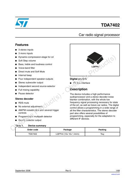
TDA7402<br />
<strong>Car</strong> <strong>radio</strong> <strong>signal</strong> <strong>processor</strong><br />
■ I 2 C bus interface<br />
Description<br />
LQFP44<br />
The device includes a high performance<br />
audio<strong>processor</strong> and a stereo decoder-noise<br />
blanker combination, with the whole low<br />
frequency <strong>signal</strong> processing necessary for state<br />
of the art, as well as future car <strong>radio</strong>s. The digital<br />
control allows a programming in a wide range of<br />
all the filter characteristics. The stereo decoder<br />
part also offers several possibilities of<br />
programming, especially for the adaptation to<br />
different IF devices.<br />
Obsolete Product(s) - Obsolete Product(s)<br />
Order code Package Packing<br />
TDA7402 LQFP44 (10x 10x 1.4mm) Tray<br />
September 2008 Rev 6 1/69<br />
www.st.com<br />
1
Contents TDA7402<br />
Contents<br />
1 Pin connections and block diagram . . . . . . . . . . . . . . . . . . . . . . . . . . . . 7<br />
2 Electrical specifications . . . . . . . . . . . . . . . . . . . . . . . . . . . . . . . . . . . . . . 9<br />
3 Audio<strong>processor</strong> part . . . . . . . . . . . . . . . . . . . . . . . . . . . . . . . . . . . . . . . . 15<br />
2/69<br />
3.1 Audio<strong>processor</strong> part features . . . . . . . . . . . . . . . . . . . . . . . . . . . . . . . . . . 15<br />
3.2 Input stages . . . . . . . . . . . . . . . . . . . . . . . . . . . . . . . . . . . . . . . . . . . . . . . 16<br />
3.2.1 Full differential stereo input 1 (FD1) . . . . . . . . . . . . . . . . . . . . . . . . . . . . 17<br />
3.2.2 Full differential stereo input 2 (FD2) . . . . . . . . . . . . . . . . . . . . . . . . . . . . 17<br />
3.2.3 Mono differential input 1 (MD1) . . . . . . . . . . . . . . . . . . . . . . . . . . . . . . . 17<br />
3.2.4 Mono differential input 2 (MD2) . . . . . . . . . . . . . . . . . . . . . . . . . . . . . . . 17<br />
3.2.5 Single ended stereo input (SE1), single ended mono input (AM)<br />
and FM-MPX input . . . . . . . . . . . . . . . . . . . . . . . . . . . . . . . . . . . . . . . . . 17<br />
3.3 AutoZero . . . . . . . . . . . . . . . . . . . . . . . . . . . . . . . . . . . . . . . . . . . . . . . . . . 17<br />
3.3.1 AutoZero for stereo decoder selection . . . . . . . . . . . . . . . . . . . . . . . . . . 17<br />
3.3.2 AutoZero remain . . . . . . . . . . . . . . . . . . . . . . . . . . . . . . . . . . . . . . . . . . 18<br />
3.4 Pause detector / MUX-output . . . . . . . . . . . . . . . . . . . . . . . . . . . . . . . . . . 18<br />
3.4.1 Loudness . . . . . . . . . . . . . . . . . . . . . . . . . . . . . . . . . . . . . . . . . . . . . . . . 18<br />
3.4.2 Attenuation . . . . . . . . . . . . . . . . . . . . . . . . . . . . . . . . . . . . . . . . . . . . . . . 18<br />
3.4.3 Peak frequency . . . . . . . . . . . . . . . . . . . . . . . . . . . . . . . . . . . . . . . . . . . 19<br />
3.4.4 Loudness order . . . . . . . . . . . . . . . . . . . . . . . . . . . . . . . . . . . . . . . . . . . 19<br />
3.4.5 Flat mode . . . . . . . . . . . . . . . . . . . . . . . . . . . . . . . . . . . . . . . . . . . . . . . . 19<br />
3.5 Soft Mute . . . . . . . . . . . . . . . . . . . . . . . . . . . . . . . . . . . . . . . . . . . . . . . . . 20<br />
3.6 Soft Step volume . . . . . . . . . . . . . . . . . . . . . . . . . . . . . . . . . . . . . . . . . . . 20<br />
3.7 Bass . . . . . . . . . . . . . . . . . . . . . . . . . . . . . . . . . . . . . . . . . . . . . . . . . . . . . 21<br />
3.7.1 Attenuation . . . . . . . . . . . . . . . . . . . . . . . . . . . . . . . . . . . . . . . . . . . . . . . 21<br />
3.7.2 Center frequency . . . . . . . . . . . . . . . . . . . . . . . . . . . . . . . . . . . . . . . . . . 21<br />
3.7.3 Quality factors . . . . . . . . . . . . . . . . . . . . . . . . . . . . . . . . . . . . . . . . . . . . 22<br />
3.7.4 DC mode . . . . . . . . . . . . . . . . . . . . . . . . . . . . . . . . . . . . . . . . . . . . . . . . 22<br />
3.8 Treble . . . . . . . . . . . . . . . . . . . . . . . . . . . . . . . . . . . . . . . . . . . . . . . . . . . . 23<br />
3.8.1 Attenuation . . . . . . . . . . . . . . . . . . . . . . . . . . . . . . . . . . . . . . . . . . . . . . . 23<br />
3.8.2 Center frequency . . . . . . . . . . . . . . . . . . . . . . . . . . . . . . . . . . . . . . . . . . 23<br />
3.9 Subwoofer application . . . . . . . . . . . . . . . . . . . . . . . . . . . . . . . . . . . . . . . 24<br />
3.10 Voice band application . . . . . . . . . . . . . . . . . . . . . . . . . . . . . . . . . . . . . . . 24<br />
Obsolete Product(s) - Obsolete Product(s)
TDA7402 Contents<br />
3.11 Compander . . . . . . . . . . . . . . . . . . . . . . . . . . . . . . . . . . . . . . . . . . . . . . . . 25<br />
3.11.1 Anti-clipping . . . . . . . . . . . . . . . . . . . . . . . . . . . . . . . . . . . . . . . . . . . . . . 25<br />
3.11.2 Characteristic . . . . . . . . . . . . . . . . . . . . . . . . . . . . . . . . . . . . . . . . . . . . . 26<br />
3.11.3 I 2 C bus timing . . . . . . . . . . . . . . . . . . . . . . . . . . . . . . . . . . . . . . . . . . . . 26<br />
3.12 AC coupling . . . . . . . . . . . . . . . . . . . . . . . . . . . . . . . . . . . . . . . . . . . . . . . 27<br />
3.13 Output selector . . . . . . . . . . . . . . . . . . . . . . . . . . . . . . . . . . . . . . . . . . . . . 27<br />
3.14 Subwoofer . . . . . . . . . . . . . . . . . . . . . . . . . . . . . . . . . . . . . . . . . . . . . . . . 28<br />
3.15 Speaker attenuator and mixing . . . . . . . . . . . . . . . . . . . . . . . . . . . . . . . . 30<br />
3.16 Audio<strong>processor</strong> testing . . . . . . . . . . . . . . . . . . . . . . . . . . . . . . . . . . . . . . . 30<br />
4 Stereo decoder part . . . . . . . . . . . . . . . . . . . . . . . . . . . . . . . . . . . . . . . . 31<br />
4.1 Stereo decoder part features . . . . . . . . . . . . . . . . . . . . . . . . . . . . . . . . . . 31<br />
4.2 Stereo decoder electrical characteristics . . . . . . . . . . . . . . . . . . . . . . . . . 31<br />
4.3 Notes about the characteristics . . . . . . . . . . . . . . . . . . . . . . . . . . . . . . . . 33<br />
4.3.1 Intermodulation suppression . . . . . . . . . . . . . . . . . . . . . . . . . . . . . . . . . 33<br />
4.3.2 Traffic <strong>radio</strong> (V.F.) suppression . . . . . . . . . . . . . . . . . . . . . . . . . . . . . . . . 33<br />
4.3.3 SCA (subsidiary communications authorization) . . . . . . . . . . . . . . . . . . 33<br />
4.3.4 ACI (adjacent channel interference) . . . . . . . . . . . . . . . . . . . . . . . . . . . 34<br />
4.4 Noise blanker part . . . . . . . . . . . . . . . . . . . . . . . . . . . . . . . . . . . . . . . . . . 34<br />
4.4.1 Noise blanker part features . . . . . . . . . . . . . . . . . . . . . . . . . . . . . . . . . . 34<br />
4.5 Multipath detector . . . . . . . . . . . . . . . . . . . . . . . . . . . . . . . . . . . . . . . . . . . 37<br />
4.5.1 Multipath detector features . . . . . . . . . . . . . . . . . . . . . . . . . . . . . . . . . . 37<br />
5 Functional description of stereo decoder . . . . . . . . . . . . . . . . . . . . . . . 38<br />
5.1 Stereo decoder mute . . . . . . . . . . . . . . . . . . . . . . . . . . . . . . . . . . . . . . . . 38<br />
5.2 InGain + infilter . . . . . . . . . . . . . . . . . . . . . . . . . . . . . . . . . . . . . . . . . . . . . 39<br />
5.3 Demodulator . . . . . . . . . . . . . . . . . . . . . . . . . . . . . . . . . . . . . . . . . . . . . . . 39<br />
5.4 De-emphasis and highcut . . . . . . . . . . . . . . . . . . . . . . . . . . . . . . . . . . . . . 40<br />
5.5 PLL and pilot tone detector . . . . . . . . . . . . . . . . . . . . . . . . . . . . . . . . . . . 40<br />
5.6 Fieldstrength control . . . . . . . . . . . . . . . . . . . . . . . . . . . . . . . . . . . . . . . . . 40<br />
5.7 EVEL input and gain . . . . . . . . . . . . . . . . . . . . . . . . . . . . . . . . . . . . . . . . 40<br />
5.8 Stereo blend control . . . . . . . . . . . . . . . . . . . . . . . . . . . . . . . . . . . . . . . . . 41<br />
5.9 Highcut control . . . . . . . . . . . . . . . . . . . . . . . . . . . . . . . . . . . . . . . . . . . . . 41<br />
Obsolete Product(s) - Obsolete Product(s)<br />
6 Functional description of the noise blanker . . . . . . . . . . . . . . . . . . . . . 43<br />
3/69
Contents TDA7402<br />
4/69<br />
6.1 Trigger path FM . . . . . . . . . . . . . . . . . . . . . . . . . . . . . . . . . . . . . . . . . . . . 43<br />
6.2 Noise controlled threshold adjustment (NCT) . . . . . . . . . . . . . . . . . . . . . 43<br />
6.3 Additional threshold control mechanism . . . . . . . . . . . . . . . . . . . . . . . . . . 44<br />
6.3.1 Automatic threshold control by the stereo blend voltage . . . . . . . . . . . . 44<br />
6.3.2 Over deviation detector . . . . . . . . . . . . . . . . . . . . . . . . . . . . . . . . . . . . . 44<br />
6.3.3 Multipath level . . . . . . . . . . . . . . . . . . . . . . . . . . . . . . . . . . . . . . . . . . . . 44<br />
6.3.4 AM mode of the noiseblanker . . . . . . . . . . . . . . . . . . . . . . . . . . . . . . . . 44<br />
7 Functional description of the multipath detector . . . . . . . . . . . . . . . . . 45<br />
7.1 Quality detector . . . . . . . . . . . . . . . . . . . . . . . . . . . . . . . . . . . . . . . . . . . . 45<br />
7.2 Testmode . . . . . . . . . . . . . . . . . . . . . . . . . . . . . . . . . . . . . . . . . . . . . . . . . 46<br />
7.3 Dual MPX usage . . . . . . . . . . . . . . . . . . . . . . . . . . . . . . . . . . . . . . . . . . . 46<br />
7.3.1 Feature description . . . . . . . . . . . . . . . . . . . . . . . . . . . . . . . . . . . . . . . . 46<br />
7.3.2 Configuration . . . . . . . . . . . . . . . . . . . . . . . . . . . . . . . . . . . . . . . . . . . . . 46<br />
8 I 2 C bus interface . . . . . . . . . . . . . . . . . . . . . . . . . . . . . . . . . . . . . . . . . . . 47<br />
8.1 Interface protocol . . . . . . . . . . . . . . . . . . . . . . . . . . . . . . . . . . . . . . . . . . . 47<br />
8.2 Auto increment . . . . . . . . . . . . . . . . . . . . . . . . . . . . . . . . . . . . . . . . . . . . . 47<br />
8.3 Transmitted data (send mode) . . . . . . . . . . . . . . . . . . . . . . . . . . . . . . . . . 47<br />
8.4 Subaddress (receive mode) . . . . . . . . . . . . . . . . . . . . . . . . . . . . . . . . . . . 48<br />
8.5 Data byte specification . . . . . . . . . . . . . . . . . . . . . . . . . . . . . . . . . . . . . . . 49<br />
9 Application information . . . . . . . . . . . . . . . . . . . . . . . . . . . . . . . . . . . . . 66<br />
10 Package information . . . . . . . . . . . . . . . . . . . . . . . . . . . . . . . . . . . . . . . . 67<br />
11 Revision history . . . . . . . . . . . . . . . . . . . . . . . . . . . . . . . . . . . . . . . . . . . 68<br />
Obsolete Product(s) - Obsolete Product(s)
TDA7402 List of tables<br />
List of tables<br />
Table 1. Device summary . . . . . . . . . . . . . . . . . . . . . . . . . . . . . . . . . . . . . . . . . . . . . . . . . . . . . . . . . . 1<br />
Table 2. Electrical characteristics . . . . . . . . . . . . . . . . . . . . . . . . . . . . . . . . . . . . . . . . . . . . . . . . . . . . 9<br />
Table 3. Absolute maximum ratings . . . . . . . . . . . . . . . . . . . . . . . . . . . . . . . . . . . . . . . . . . . . . . . . . 14<br />
Table 4. Thermal data. . . . . . . . . . . . . . . . . . . . . . . . . . . . . . . . . . . . . . . . . . . . . . . . . . . . . . . . . . . . 14<br />
Table 5. Supply. . . . . . . . . . . . . . . . . . . . . . . . . . . . . . . . . . . . . . . . . . . . . . . . . . . . . . . . . . . . . . . . . 14<br />
Table 6. Attack times vs. soft-step times . . . . . . . . . . . . . . . . . . . . . . . . . . . . . . . . . . . . . . . . . . . . . 26<br />
Table 7. Stereo decoder electrical characteristics . . . . . . . . . . . . . . . . . . . . . . . . . . . . . . . . . . . . . . 31<br />
Table 8. Noise blanker electrical characteristics. . . . . . . . . . . . . . . . . . . . . . . . . . . . . . . . . . . . . . . . 34<br />
Table 9. Multipath detector electrical characteristics . . . . . . . . . . . . . . . . . . . . . . . . . . . . . . . . . . . . 37<br />
Table 10. Transmitted data (send mode) . . . . . . . . . . . . . . . . . . . . . . . . . . . . . . . . . . . . . . . . . . . . . . 47<br />
Table 11. Reset condition . . . . . . . . . . . . . . . . . . . . . . . . . . . . . . . . . . . . . . . . . . . . . . . . . . . . . . . . . . 47<br />
Table 12. Subaddress (receive mode) . . . . . . . . . . . . . . . . . . . . . . . . . . . . . . . . . . . . . . . . . . . . . . . . 48<br />
Table 13. Main selector (0) . . . . . . . . . . . . . . . . . . . . . . . . . . . . . . . . . . . . . . . . . . . . . . . . . . . . . . . . . 49<br />
Table 14. Main loudness (1) . . . . . . . . . . . . . . . . . . . . . . . . . . . . . . . . . . . . . . . . . . . . . . . . . . . . . . . . 49<br />
Table 15. Volume (2) . . . . . . . . . . . . . . . . . . . . . . . . . . . . . . . . . . . . . . . . . . . . . . . . . . . . . . . . . . . . . 50<br />
Table 16. Treble filter (3) . . . . . . . . . . . . . . . . . . . . . . . . . . . . . . . . . . . . . . . . . . . . . . . . . . . . . . . . . . 50<br />
Table 17. Bass filter (4). . . . . . . . . . . . . . . . . . . . . . . . . . . . . . . . . . . . . . . . . . . . . . . . . . . . . . . . . . . . 51<br />
Table 18. Mixing programming (5) . . . . . . . . . . . . . . . . . . . . . . . . . . . . . . . . . . . . . . . . . . . . . . . . . . . 51<br />
Table 19. Soft mute (6) . . . . . . . . . . . . . . . . . . . . . . . . . . . . . . . . . . . . . . . . . . . . . . . . . . . . . . . . . . . . 52<br />
Table 20. Voiceband (7) . . . . . . . . . . . . . . . . . . . . . . . . . . . . . . . . . . . . . . . . . . . . . . . . . . . . . . . . . . . 52<br />
Table 21. Second source selector (8). . . . . . . . . . . . . . . . . . . . . . . . . . . . . . . . . . . . . . . . . . . . . . . . . 53<br />
Table 22. Second loudness (9). . . . . . . . . . . . . . . . . . . . . . . . . . . . . . . . . . . . . . . . . . . . . . . . . . . . . . 54<br />
Table 23. Subwoofer configuration / Bass (10). . . . . . . . . . . . . . . . . . . . . . . . . . . . . . . . . . . . . . . . . . 54<br />
Table 24. Compander (11) . . . . . . . . . . . . . . . . . . . . . . . . . . . . . . . . . . . . . . . . . . . . . . . . . . . . . . . . . 55<br />
Table 25. Configuration audio<strong>processor</strong> I (12) . . . . . . . . . . . . . . . . . . . . . . . . . . . . . . . . . . . . . . . . . . 55<br />
Table 26. Configuration audio<strong>processor</strong> II (13) . . . . . . . . . . . . . . . . . . . . . . . . . . . . . . . . . . . . . . . . . 56<br />
Table 27. Speaker, subwoofer and mixer level-control (14-20) . . . . . . . . . . . . . . . . . . . . . . . . . . . . . 57<br />
Table 28. Testing Audio<strong>processor</strong> (21). . . . . . . . . . . . . . . . . . . . . . . . . . . . . . . . . . . . . . . . . . . . . . . . 58<br />
Table 29. Stereo decoder (22) . . . . . . . . . . . . . . . . . . . . . . . . . . . . . . . . . . . . . . . . . . . . . . . . . . . . . . 58<br />
Table 30. Noise blanker I (23) . . . . . . . . . . . . . . . . . . . . . . . . . . . . . . . . . . . . . . . . . . . . . . . . . . . . . . 59<br />
Table 31. Noiseblanker II (24) . . . . . . . . . . . . . . . . . . . . . . . . . . . . . . . . . . . . . . . . . . . . . . . . . . . . . . 60<br />
Table 32. AM / FM noiseblanker (25) . . . . . . . . . . . . . . . . . . . . . . . . . . . . . . . . . . . . . . . . . . . . . . . . . 60<br />
Table 33. High cut (26) . . . . . . . . . . . . . . . . . . . . . . . . . . . . . . . . . . . . . . . . . . . . . . . . . . . . . . . . . . . . 61<br />
Table 34. Fieldstrength control (27) . . . . . . . . . . . . . . . . . . . . . . . . . . . . . . . . . . . . . . . . . . . . . . . . . . 62<br />
Table 35. Multipath detector (28) . . . . . . . . . . . . . . . . . . . . . . . . . . . . . . . . . . . . . . . . . . . . . . . . . . . . 62<br />
Table 36. Stereo decoder adjustment (29) . . . . . . . . . . . . . . . . . . . . . . . . . . . . . . . . . . . . . . . . . . . . . 63<br />
Obsolete Product(s) - Obsolete Product(s)<br />
Table 37. Stereo decoder configuration (30) . . . . . . . . . . . . . . . . . . . . . . . . . . . . . . . . . . . . . . . . . . . 64<br />
Table 38. Testing stereo decoder (31) . . . . . . . . . . . . . . . . . . . . . . . . . . . . . . . . . . . . . . . . . . . . . . . . 65<br />
Table 39. Document revision history . . . . . . . . . . . . . . . . . . . . . . . . . . . . . . . . . . . . . . . . . . . . . . . . . 68<br />
5/69
List of figures TDA7402<br />
List of figures<br />
Figure 1. Pin connections (top view) . . . . . . . . . . . . . . . . . . . . . . . . . . . . . . . . . . . . . . . . . . . . . . . . . . 7<br />
Figure 2. Block diagram . . . . . . . . . . . . . . . . . . . . . . . . . . . . . . . . . . . . . . . . . . . . . . . . . . . . . . . . . . . . 8<br />
Figure 3. Input-stages . . . . . . . . . . . . . . . . . . . . . . . . . . . . . . . . . . . . . . . . . . . . . . . . . . . . . . . . . . . . 16<br />
Figure 4. Loudness attenuation @ fP = 400Hz.. . . . . . . . . . . . . . . . . . . . . . . . . . . . . . . . . . . . . . . . . 18<br />
Figure 5. Loudness center frequencies @ Attn. = 15dB. . . . . . . . . . . . . . . . . . . . . . . . . . . . . . . . . . . 19<br />
Figure 6. 1 st and 2 nd order loudness @ Attn. = 15dB, fP=400Hz . . . . . . . . . . . . . . . . . . . . . . . . . . . 19<br />
Figure 7. Soft Mute timing . . . . . . . . . . . . . . . . . . . . . . . . . . . . . . . . . . . . . . . . . . . . . . . . . . . . . . . . . 20<br />
Figure 8. Soft Step timing . . . . . . . . . . . . . . . . . . . . . . . . . . . . . . . . . . . . . . . . . . . . . . . . . . . . . . . . . 20<br />
Figure 9. Bass control @ fC = 80Hz, Q = 1 . . . . . . . . . . . . . . . . . . . . . . . . . . . . . . . . . . . . . . . . . . . . 21<br />
Figure 10. Bass center frequencies @ gain = 14dB, Q = 1 . . . . . . . . . . . . . . . . . . . . . . . . . . . . . . . . . 21<br />
Figure 11. Bass quality factors @ Gain = 14dB, fC = 80Hz. . . . . . . . . . . . . . . . . . . . . . . . . . . . . . . . . 22<br />
Figure 12. Bass normal and DC Mode @ Gain = 14dB, fC = 80Hz. . . . . . . . . . . . . . . . . . . . . . . . . . . 22<br />
Figure 13. Treble control @ fC = 17.5kHz . . . . . . . . . . . . . . . . . . . . . . . . . . . . . . . . . . . . . . . . . . . . . . 23<br />
Figure 14. Treble center frequencies @ gain = 14dB . . . . . . . . . . . . . . . . . . . . . . . . . . . . . . . . . . . . . 23<br />
Figure 15. Subwoofer application with LPF 80/120/160Hz and HPF 90/135/180Hz . . . . . . . . . . . . . . 24<br />
Figure 16. Voiceband application with HPF 300/450/600/750Hz and LPF 3k/6kHz . . . . . . . . . . . . . . 24<br />
Figure 17. Compander block diagram . . . . . . . . . . . . . . . . . . . . . . . . . . . . . . . . . . . . . . . . . . . . . . . . . 25<br />
Figure 18. Compander characteristic. . . . . . . . . . . . . . . . . . . . . . . . . . . . . . . . . . . . . . . . . . . . . . . . . . 26<br />
Figure 19. Output selector . . . . . . . . . . . . . . . . . . . . . . . . . . . . . . . . . . . . . . . . . . . . . . . . . . . . . . . . . . 27<br />
Figure 20. Application 1 using internal highpass and mono low pass filter . . . . . . . . . . . . . . . . . . . . . 28<br />
Figure 21. Application 2 using internal highpass and external stereo low pass filter. . . . . . . . . . . . . . 29<br />
Figure 22. Application 3 using pure external filtering (e.g. DSP) . . . . . . . . . . . . . . . . . . . . . . . . . . . . . 29<br />
Figure 23. Output selector . . . . . . . . . . . . . . . . . . . . . . . . . . . . . . . . . . . . . . . . . . . . . . . . . . . . . . . . . . 30<br />
Figure 24. Vn timing diagram. . . . . . . . . . . . . . . . . . . . . . . . . . . . . . . . . . . . . . . . . . . . . . . . . . . . . . . . 36<br />
Figure 25. Trigger threshold vs. VPEAK . . . . . . . . . . . . . . . . . . . . . . . . . . . . . . . . . . . . . . . . . . . . . . . 36<br />
Figure 26. Deviation controlled trigger adjustment . . . . . . . . . . . . . . . . . . . . . . . . . . . . . . . . . . . . . . . 36<br />
Figure 27. Field strength controlled trigger adjustment . . . . . . . . . . . . . . . . . . . . . . . . . . . . . . . . . . . . 36<br />
Figure 28. Block diagram of stereo decoder . . . . . . . . . . . . . . . . . . . . . . . . . . . . . . . . . . . . . . . . . . . . 38<br />
Figure 29. Signals during stereo decoder's Soft Mute . . . . . . . . . . . . . . . . . . . . . . . . . . . . . . . . . . . . . 39<br />
Figure 30. Signal control via Soft Mute pin . . . . . . . . . . . . . . . . . . . . . . . . . . . . . . . . . . . . . . . . . . . . . 39<br />
Figure 31. Internal stereo blend characteristics . . . . . . . . . . . . . . . . . . . . . . . . . . . . . . . . . . . . . . . . . . 41<br />
Figure 32. Relation between internal and external LEVEL voltages for setup of stereo blend . . . . . . 41<br />
Figure 33. Highcut characteristics . . . . . . . . . . . . . . . . . . . . . . . . . . . . . . . . . . . . . . . . . . . . . . . . . . . . 42<br />
Figure 34. Block diagram of the noise blanker. . . . . . . . . . . . . . . . . . . . . . . . . . . . . . . . . . . . . . . . . . . 43<br />
Figure 35. Block diagram of the multipath detector . . . . . . . . . . . . . . . . . . . . . . . . . . . . . . . . . . . . . . . 45<br />
Figure 36. Dual MPX input diagram. . . . . . . . . . . . . . . . . . . . . . . . . . . . . . . . . . . . . . . . . . . . . . . . . . . 46<br />
Obsolete Product(s) - Obsolete Product(s)<br />
Figure 37. Application diagram (standard configuration) . . . . . . . . . . . . . . . . . . . . . . . . . . . . . . . . . . . 66<br />
Figure 38. Application diagram (Dual MPX mode). . . . . . . . . . . . . . . . . . . . . . . . . . . . . . . . . . . . . . . . 66<br />
Figure 39. LQFP44 (10x10) mechanical data and package dimensions . . . . . . . . . . . . . . . . . . . . . . . 67<br />
6/69
TDA7402 Pin connections and block diagram<br />
1 Pin connections and block diagram<br />
Figure 1. Pin connections (top view)<br />
SE1L<br />
SE1R<br />
FD1L+/SE3L<br />
FD1L-/SE2L<br />
FD1R+/SE3R<br />
FD1R-/SE2R<br />
FD2L+<br />
FD2L-<br />
FD2R+<br />
FD2R-<br />
AM<br />
1<br />
2<br />
3<br />
4<br />
5<br />
6<br />
7<br />
8<br />
9<br />
10<br />
11<br />
AM IF<br />
MD2G<br />
MPX<br />
MD2<br />
LEVEL<br />
MD1G/SE4L<br />
MPIN<br />
MD1/SE4R<br />
MPOUT<br />
MUX/PAUSE<br />
QUAL<br />
CREF<br />
SM<br />
ACOUTL<br />
GND<br />
ACOUTR<br />
SDA<br />
SWINL<br />
SCL<br />
SWINR<br />
VDD ACINLF<br />
44 43 42 41 40 39 38 37 36 35 34<br />
12 13 14 15 16<br />
17<br />
18 19 20 21 22<br />
33<br />
32<br />
31<br />
30<br />
29<br />
28<br />
27<br />
26<br />
25<br />
24<br />
23<br />
D00AU1131<br />
ACINLR<br />
ACINRF<br />
ACINRR<br />
OUTLF<br />
OUTLR<br />
OUTRF<br />
OUTRR<br />
OUTSWL<br />
OUTSWR<br />
OUTSSL<br />
OUTSSR<br />
Obsolete Product(s) - Obsolete Product(s)<br />
7/69
Pin connections and block diagram TDA7402<br />
8/69<br />
Figure 2. Block diagram<br />
ACINLF<br />
ACINLR<br />
ACINRF<br />
ACINRR<br />
SWINL<br />
SWINR<br />
ACOUTR<br />
ACOUTL<br />
SM<br />
MUX<br />
FD1L+<br />
FD1L-<br />
FD1R+<br />
ACIN<br />
FD1R-<br />
VOICE BANDPASS<br />
CHG<br />
OUTLF<br />
OUTLR<br />
MONO-FADER<br />
MONO-FADER<br />
FRONT<br />
TREBLE<br />
SOFT<br />
MUTE<br />
LOUDNESS<br />
IN-GAIN<br />
+ AUTO<br />
ZERO<br />
MAIN<br />
SOURCE<br />
SELECTOR<br />
FD2L+<br />
FD2L-<br />
OUTPUT<br />
SELECTOR<br />
REAR<br />
SW<br />
BASS<br />
SOFT<br />
STEP<br />
VOLUME<br />
+<br />
MIXER<br />
HP LP<br />
AUX<br />
OUTRF<br />
OUTRR<br />
MONO-FADER<br />
MONO-FADER<br />
FD2R+<br />
FD2R-<br />
INPUT-<br />
MULTIPLEXER<br />
SEL<br />
MAIN<br />
SER<br />
COMPANDER<br />
MIXING<br />
SELECTOR<br />
OUTSWL<br />
OUTSWR<br />
MONO-FADER<br />
MONO-FADER<br />
SUBWOOFER<br />
+ PHONE<br />
CONTROL<br />
ANTI CLIP.<br />
INPUT<br />
MD1<br />
NAVI<br />
MD1G<br />
MD2<br />
OUTSSL<br />
PHONE<br />
MD2G<br />
LOUDNESS<br />
MUTE IN GAIN<br />
SECOND<br />
SOURCE<br />
SELECTOR<br />
OUTSSR<br />
AM<br />
SEN<br />
SDA<br />
SCL<br />
DIGITAL CONTROL IIC BUS<br />
PAUSE<br />
BEEP<br />
25KHz<br />
LP<br />
DEMODULATOR<br />
+ STEREO ADJUST<br />
+ STEREO BLEND<br />
PILOT<br />
CANCELLATION<br />
80KHz<br />
LP<br />
MPX<br />
QUAL<br />
PIL.<br />
DET.<br />
PLL<br />
MULTIPATH<br />
DETECTOR<br />
VDD<br />
GND<br />
CREF<br />
Obsolete Product(s) - Obsolete Product(s)<br />
HIGH<br />
CUT<br />
S & H<br />
QUAL.<br />
SUPPLY<br />
D<br />
A<br />
PULSE<br />
FORMER<br />
AM/FM<br />
NOISE<br />
BANKER<br />
AM-IF<br />
LEVEL D00AU1130<br />
MPOUT<br />
MPIN
TDA7402 Electrical specifications<br />
2 Electrical specifications<br />
V S = 9V; T amb = 25°C; R L = 10kΩ; all gains = 0dB; f = 1kHz; unless otherwise specified.<br />
Table 2. Electrical characteristics<br />
Symbol Parameter Test condition Min. Typ. Max. Unit<br />
Input selector<br />
R in Input resistance all single ended Inputs 70 100 130 kΩ<br />
VCL Clipping level 2.2 2.6 VRMS SIN Input separation 80 100 dB<br />
G IN MIN Min. input gain -1 0 +1 dB<br />
G IN MAX Max. input gain 13 15 17 dB<br />
G STEP Step resolution 0.5 1 1.5 dB<br />
V DC<br />
DC steps<br />
Adjacent gain steps -5 1 5 mV<br />
G MIN to G MAX -10 6 10 mV<br />
V offset Remaining offset with autozero 0.5 mV<br />
Differential stereo inputs<br />
R in<br />
Input resistance<br />
(see Figure 3)<br />
G CD Gain only at true differential input<br />
CMRR Common mode rejection ratio<br />
Differential 70 100 130 kΩ<br />
-1 0 1 dB<br />
-5 -6 7 dB<br />
-11 -12 -13 dB<br />
V CM = 1V RMS @ 1kHz 46 70 dB<br />
V CM = 1V RMS @ 10kHz 46 60 dB<br />
e NO Output-noise @ speaker outputs 20Hz - 20kHz, flat; all stages 0dB 9 15 µV<br />
Differential mono inputs<br />
R in Input impedance Differential 40 56 72 kΩ<br />
Obsolete Product(s) - Obsolete Product(s)<br />
CMRR Common mode rejection ratio<br />
Beep control<br />
V CM = 1V RMS @ 1kHz 40 70 dB<br />
V CM = 1V RMS @ 10kHz 40 60 dB<br />
V RMS Beep level Mix-gain = 6dB 250 350 500 mV<br />
f Beep<br />
Beep frequency<br />
f Beep1 570 600 630 Hz<br />
f Beep2 740 780 820 Hz<br />
f Beep1 1.48 1.56 1.64 kHz<br />
f Beep1 2.28 2.4 2.52 kHz<br />
9/69
Electrical specifications TDA7402<br />
Table 2. Electrical characteristics (continued)<br />
Symbol Parameter Test condition Min. Typ. Max. Unit<br />
Mixing control<br />
M LEVEL Mixing ratio Main / mix source -6/-6 dB<br />
G MAX Max. gain 13 15 17 dB<br />
A MAX Max. attenuation -83 -79 -75 dB<br />
A STEP Attenuation step 0.5 1 1.5 dB<br />
Multiplexer output (1)<br />
R OUT Output impedance 225 300 W<br />
10/69<br />
R L Output load resistance 2 kΩ<br />
C L Output load capacitance 10 nF<br />
V DC DC voltage level 4.3 4.5 4.7 V<br />
Loudness control<br />
A STEP Step resolution 0.5 1 1.5 dB<br />
A MAX Max. attenuation -21 -19 -17 dB<br />
f Peak<br />
Volume control<br />
Peak frequency<br />
f P1 180 200 220 Hz<br />
f P2 360 400 440 Hz<br />
f P3 540 600 660 Hz<br />
f P4 720 800 880 Hz<br />
G MAX Max. gain 30 32 34 dB<br />
A MAX Max. attenuation -83 -79.5 -75 dB<br />
A STEP Step resolution 0 0.5 1 dB<br />
E A<br />
Attenuation set error<br />
G = -20 to +20dB -0.75 0 +0.75 dB<br />
G = -80 to -20dB -4 0 3 dB<br />
E T Tracking error 2 dB<br />
Obsolete Product(s) - Obsolete Product(s)<br />
V DC<br />
Soft mute<br />
DC steps<br />
Adjacent attenuation steps 0.1 3 mV<br />
From 0dB to G MIN 0.5 5 mV<br />
A MUTE Mute attenuation 80 100 dB<br />
T D<br />
Delay time<br />
T1 0.48 1 ms<br />
T2 0.96 2 ms<br />
T3 70 123 170 ms<br />
T4 200 324 600 ms<br />
V TH low Low threshold for SM Pin (2) 1 V<br />
V TH high High threshold for SM Pin 2.5 V
TDA7402 Electrical specifications<br />
Table 2. Electrical characteristics (continued)<br />
Symbol Parameter Test condition Min. Typ. Max. Unit<br />
R PU Internal pull-up resistor 32 45 58 kΩ<br />
V PU Internal pull-up voltage 3.3 V<br />
Bass control<br />
C RANGE Control range +14 +15 +16 dB<br />
A STEP Step resolution 0.5 1 1.5 dB<br />
f C<br />
Q BASS<br />
Center frequency<br />
Quality factor<br />
DC GAIN Bass-DC-gain<br />
Treble control<br />
f C1 54 60 66 Hz<br />
f C2 63 70 77 Hz<br />
f C3 72 80 88 Hz<br />
f C4 81 90 99 Hz<br />
f C5 90 100 110 Hz<br />
f C6 117 130 143 Hz<br />
f C7 135 150 165 Hz<br />
f C8 180 200 220 Hz<br />
Q 1 0.9 1 1.1<br />
Q 2 1.1 1.25 1.4<br />
Q 3 1.3 1.5 1.7<br />
Q 4 1.8 2 2.2<br />
DC = off -1 0 +1 dB<br />
DC = on 4 4.4 6 dB<br />
C RANGE Control range +14 +15 +16 dB<br />
A STEP Step resolution 0.5 1 1.5 dB<br />
f C<br />
Pause detector (3)<br />
V TH<br />
Center frequency<br />
Zero crossing threshold<br />
f C1 8 10 12 kHz<br />
f C2 10 12.5 15 kHz<br />
f C3 12 15 18 kHz<br />
Obsolete Product(s) - Obsolete Product(s)<br />
f C4 14 17.5 21 kHz<br />
Window 1 40 mV<br />
Window 2 80 mV<br />
Window 3 160 mV<br />
I DELAY Pull-up current 15 25 35 μA<br />
V THP Pause threshold 3.0 V<br />
11/69
Electrical specifications TDA7402<br />
Table 2. Electrical characteristics (continued)<br />
Symbol Parameter Test condition Min. Typ. Max. Unit<br />
Speaker attenuator<br />
12/69<br />
R in Input impedance 35 50 65 kΩ<br />
G MAX Max. gain 14 15 16 dB<br />
A MAX Max. attenuation -83 -79 -75 dB<br />
A STEP Step resolution 0.5 1 1.5 dB<br />
A MUTE Output mute attenuation 80 90 dB<br />
E E Attenuation set error 2 dB<br />
V DC DC steps Adjacent attenuation steps 0.1 5 mV<br />
Audio outputs<br />
VCLIP Clipping level d = 0.3% 2.2 2.6 VRMS RL Output load resistance 2 kΩ<br />
C L Output load capacitance 10 nF<br />
R OUT Output impedance 30 100 W<br />
V DC DC voltage level 4.3 4.5 4.7 V<br />
Voice bandpass<br />
f HP<br />
f LP<br />
Highpass corner frequency<br />
Lowpass corner frequency<br />
Subwoofer attenuator<br />
f HP1 81 90 99 Hz<br />
f HP2 122 135 148 Hz<br />
f HP3 162 180 198 Hz<br />
f HP4 194 215 236 Hz<br />
f HP5 270 300 330 Hz<br />
f HP6 405 450 495 Hz<br />
f HP7 540 600 660 Hz<br />
f HP8 675 750 825 Hz<br />
f LP1 2.7 3 3.3 kHz<br />
f LP2 5.4 6 6.6 kHz<br />
Obsolete Product(s) - Obsolete Product(s)<br />
R in Input impedance 35 50 65 kΩ<br />
G MAX Max. gain 14 15 16 dB<br />
A ATTN Max. attenuation -83 -79 -75 dB<br />
A STEP Step resolution 0.5 1 1.5 dB<br />
A MUTE Output mute attenuation 80 90 dB<br />
E E Attenuation set error 2 dB<br />
V DC DC steps Adjacent attenuation steps 1 5 mV
TDA7402 Electrical specifications<br />
Table 2. Electrical characteristics (continued)<br />
Symbol Parameter Test condition Min. Typ. Max. Unit<br />
Subwoofer lowpass<br />
f LP<br />
Lowpass corner frequency<br />
Differential outputs (4)<br />
R L<br />
R DL<br />
load resistance at each output<br />
load resistance differential<br />
f LP1 72 80 88 Hz<br />
f LP2 108 120 132 Hz<br />
f LP3 144 160 176 Hz<br />
1V RMS ; AC coupled; THD=1% 1 kΩ<br />
2V RMS; AC coupled; THD=1% 2 kΩ<br />
1V RMS ; AC coupled; THD=1% 2 kΩ<br />
2V RMS ; AC coupled; THD=1% 4 kΩ<br />
C LMAX Capacitive load at each output C Lmax at each output to ground 10 nF<br />
C DLMAX Capacitive load differential C Lmax between output terminals 5 nF<br />
V Offset DC offset at pins Output muted -10 10 mV<br />
R OUT Output impedance 30 100 W<br />
V DC DC voltage level 4.3 4.5 4.7 V<br />
e NO Output noise Output muted 6 15 µV<br />
Compander<br />
G MAX<br />
t Att<br />
t Rel<br />
V REF<br />
max. compander gain<br />
Attack time<br />
Release time<br />
Compander reference input-level<br />
(equals 0dB)<br />
Vi < -46dB 19 dB<br />
Vi < -46dB, Anti-clip = on 29 dB<br />
t Att1 6 ms<br />
t Att2 12 ms<br />
t Att3 24 ms<br />
t Att4 49 ms<br />
t Rel1 390 ms<br />
t Rel2 780 ms<br />
t Rel3 1.17 s<br />
Obsolete Product(s) - Obsolete Product(s)<br />
t Rel4 1.56 s<br />
V REF1 0.5 V RMS<br />
V REF2 1.0 V RMS<br />
V REF3 2.0 V RMS<br />
C F Compression factor Output <strong>signal</strong> / input <strong>signal</strong> 0.5<br />
13/69
Electrical specifications TDA7402<br />
Table 2. Electrical characteristics (continued)<br />
Symbol Parameter Test condition Min. Typ. Max. Unit<br />
General<br />
e NO<br />
14/69<br />
Output noise<br />
BW = 20Hz - 20kHz<br />
output muted<br />
all gains = 0dB single ended<br />
inputs<br />
S/N Signal to noise ratio<br />
all gains = 0dB<br />
flat; VO = 2VRMS bass, treble at +12dB;<br />
a-weighted; VO = 2.6VRMS 106<br />
100<br />
dB<br />
dB<br />
VIN = 1VRMS; all stages 0dB 0.005 0.1 %<br />
d distortion<br />
VOUT = 1VRMS ; bass & treble =<br />
12dB<br />
0.05 0.1 %<br />
SC Channel separation left/right 80 100 dB<br />
E T<br />
Total tracking error<br />
1. If configured as multiplexer-output<br />
2. The SM Pin is active low (mute = 0)<br />
3. If configured as pause-output<br />
4. If programmed as subwoofer diff. output<br />
Table 3. Absolute maximum ratings<br />
3<br />
10<br />
15<br />
20<br />
A V = 0 to -20dB -1 0 1 dB<br />
A V = -20 to -60dB -2 0 2 dB<br />
Symbol Parameter Value Unit<br />
V S Operating supply voltage 10.5 V<br />
T amb Operating temperature range -40 to 85 °C<br />
T stg Storage temperature range -55 to +150 °C<br />
V ESD ESD protection (human body mode) ±2000 V<br />
V ESD ESD protection (machine mode) ±200 V<br />
Table 4. Thermal data<br />
Obsolete Product(s) - Obsolete Product(s)<br />
Symbol Parameter Value Unit<br />
R th j-pins Thermal resistance junction-pins max 65 °C/W<br />
Table 5. Supply<br />
Symbol Parameter Test condition Min. Typ. Max. Unit<br />
V S Supply voltage 7.5 9 10 V<br />
I S Supply current V S = 9V 35 50 65 mA<br />
SVRR Ripple rejection @ 1kHz<br />
Audio<strong>processor</strong><br />
(all Filters flat)<br />
60 dB<br />
µV<br />
µV
TDA7402 Audio<strong>processor</strong> part<br />
3 Audio<strong>processor</strong> part<br />
3.1 Audio<strong>processor</strong> part features<br />
● Input multiplexer<br />
– 2 fully differential CD stereo inputs with programmable attenuation<br />
– 1 single ended stereo input<br />
– 2 differential mono input<br />
– 1 single ended mono input<br />
– In-gain 0..15dB, 1dB steps<br />
– internal offset cancellation (AutoZero)<br />
– separate second source selector<br />
● Beep<br />
– internal beep with 4 frequencies<br />
● Mixing stage<br />
– Beep, phone and navigation mixable to all speaker outputs<br />
● Loudness<br />
– programmable center frequency and frequency response<br />
– 15 x 1dB steps<br />
– selectable flat-mode (constant attenuation)<br />
● Volume<br />
– 0.5dB attenuator<br />
– 100dB range<br />
– soft-step control with programmable times<br />
● Compander<br />
– dynamic range compression for use with CD<br />
– 2:1 compression rate<br />
– programmable max. gain<br />
● Bass<br />
– 2nd order frequency response<br />
– center frequency programmable in 8 steps<br />
– DC gain programmable<br />
– + 15 x 1dB steps<br />
● Treble<br />
– 2nd order frequency response<br />
– center frequency programmable in 4 steps<br />
– +15 x 1dB steps<br />
● Voice bandpass<br />
– 2nd order butterworth highpass filter with programmable cut off frequency<br />
– 2nd order butterworth lowpass filter with programmable cut off frequency<br />
– selectable flat mode<br />
Obsolete Product(s) - Obsolete Product(s)<br />
15/69
Audio<strong>processor</strong> part TDA7402<br />
16/69<br />
● Speaker<br />
– 4 independent speaker controls in 1dB steps<br />
– control range 95dB<br />
– separate Mute<br />
● Subwoofer<br />
– single ended stereo output<br />
– independent stereo level controls in 1dB steps<br />
– control range 95dB<br />
– separate Mute<br />
● Mute Functions<br />
– direct mute<br />
– digitally controlled Soft Mute with 4 programmable mute-times<br />
● Pause Detector<br />
– programmable threshold<br />
3.2 Input stages<br />
In the basic configuration two full differential, two mono differential, one single ended stereo<br />
and one single ended mono input are available. In addition a dedicated input for the stereo<br />
decoder MPX <strong>signal</strong> is present.<br />
Figure 3. Input-stages<br />
SE2<br />
FD1-<br />
STEREO<br />
FD1+<br />
SE3<br />
FD2-<br />
STEREO<br />
FD2+<br />
SE4<br />
MD1G<br />
MONO<br />
MD1<br />
SE4R<br />
SE1<br />
STEREO<br />
AM<br />
MONO<br />
MPX<br />
100K<br />
100K<br />
100K<br />
100K<br />
100K<br />
100K<br />
100K<br />
100K<br />
100K<br />
100K<br />
1<br />
1<br />
1<br />
1<br />
15K 15K<br />
-<br />
+<br />
15K 15K<br />
15K 15K<br />
-<br />
+<br />
15K 15K<br />
28K 28K<br />
-<br />
+<br />
28K 28K<br />
28K 28K<br />
-<br />
+<br />
28K 28K<br />
SE4R<br />
MAIN SOURCE<br />
SELECTOR<br />
SE3<br />
FD1/SE2<br />
FD2<br />
MD1/SE4<br />
MUTE<br />
MD2<br />
SE1<br />
100K<br />
AM<br />
FM<br />
MD2<br />
MD1<br />
FM<br />
BEEP<br />
SE3<br />
FD1/SE2<br />
FD2<br />
MD1/SE4<br />
MD2<br />
SE1<br />
AM<br />
FM<br />
MIXING<br />
SELECTOR<br />
MUTE<br />
SECOND SOURCE<br />
SELECTOR<br />
MUTE<br />
IN GAIN<br />
MIXING STAGE<br />
Obsolete Product(s) - Obsolete Product(s)<br />
MD2G<br />
MONO<br />
MD2<br />
100K<br />
NOISE BLANKER<br />
+<br />
STEREO DECODER<br />
D00AU1142<br />
IN GAIN
TDA7402 Audio<strong>processor</strong> part<br />
3.2.1 Full differential stereo input 1 (FD1)<br />
The FD1 input is implemented as a buffered full-differential stereo stage with 100kΩ input<br />
impedance at each input. The attenuation is programmable in 3 steps from 0 to -12dB in<br />
order to adapt the incoming <strong>signal</strong> level. A 6dB attenuation is included in the differential<br />
stage, the additional 6dB are done by a following resistive divider. This input is also<br />
configurable as two single ended stereo inputs (see pin-out).<br />
3.2.2 Full differential stereo input 2 (FD2)<br />
The FD2 input has the same general structure as FD1, but with a programmable attenuation<br />
of 0 or 6dB embedded in the differential stage.<br />
3.2.3 Mono differential input 1 (MD1)<br />
The MD1 input is designed as a basic differential stage with 56kΩ input impedance. This<br />
input is configurable as a single ended stereo input (see pin-out).<br />
3.2.4 Mono differential input 2 (MD2)<br />
The MD2 input has the same topology as MD1, but without the possibility to configure it to<br />
single ended.<br />
3.2.5 Single ended stereo input (SE1), single ended mono input (AM) and<br />
FM-MPX input<br />
All single ended inputs offer an input impedance of 100kΩ. The AM pin can be connected by<br />
software to the input of the stereo-decoder in order to use the AM noiseblanker and AM High<br />
Cut feature.<br />
3.3 AutoZero<br />
The AutoZero allows a reduction of the number of pins as well as external components by<br />
canceling any offset generated by or before the In-Gain-stage (Please notice that externally<br />
generated offsets, e.g. generated through the leakage current of the coupling capacitors,<br />
are not canceled).<br />
The auto zeroing is started every time the DATA-BYTE 0 is selected and needs max. 0.3ms<br />
for the alignment. To avoid audible clicks the Audio<strong>processor</strong> is muted before the loudness<br />
stage during this time. The AutoZero feature is only present in the main <strong>signal</strong> path.<br />
Obsolete Product(s) - Obsolete Product(s)<br />
3.3.1 AutoZero for stereo decoder selection<br />
A special procedure is recommended for selecting the stereo decoder at the main inputselector<br />
to guarantee an optimum offset cancellation:<br />
1. Soft Mute or Mute the <strong>signal</strong>-path<br />
2. Temporary deselect the stereo decoder at all input selectors<br />
3. Configure the stereo decoder via IIC-Bus<br />
4. Wait 1ms<br />
5. Select the stereo decoder at the main input selector first<br />
17/69
Audio<strong>processor</strong> part TDA7402<br />
18/69<br />
The root cause of this procedure is, that after muting the stereo decoder (Step 1), the<br />
internal stereo decoder filters have to settle in order to perform a proper offset cancellation.<br />
3.3.2 AutoZero remain<br />
In some cases, for example if the µP is executing a refresh cycle of the I 2 C Bus<br />
programming, it is not useful to start a new AutoZero action because no new source is<br />
selected and an undesired mute would appear at the outputs. For such applications the<br />
TDA7402 could be switched in the AutoZero Remain Mode (Bit 6 of the subaddress byte).<br />
If this bit is set to high, the DATABYTE 0 could be loaded without invoking the AutoZero and<br />
the old adjustment value remains.<br />
3.4 Pause detector / MUX-output<br />
The pin number 40 (Pause/MUX) is configurable for two different functions:<br />
1. During pause detector OFF this pin is used as a mono output of the main input selector.<br />
This <strong>signal</strong> is often used to drive a level/equalizer display on the car <strong>radio</strong> front panel.<br />
2. During pause detector ON the pin is used to define the time constant of the detector by<br />
an external capacitor. The pause detector is driven by the internal stereo decoder<br />
outputs in order to use pauses in the FM <strong>signal</strong> for alternate frequency jumps. If the<br />
<strong>signal</strong> level of both stereo decoder channels is outside the programmed voltage<br />
window, the external capacitor is abruptly discharged. Inside the pause condition the<br />
capacitor is slowly recharged by a constant current of 25µA. The pause information is<br />
also available via I 2 C Bus (see I 2 C Bus programming).<br />
3.4.1 Loudness<br />
There are four parameters programmable in the loudness stage:<br />
3.4.2 Attenuation<br />
Figure 4 shows the attenuation as a function of frequency at f P = 400Hz<br />
Figure 4. Loudness attenuation @ f P = 400Hz.<br />
dB<br />
0.0<br />
Obsolete Product(s) - Obsolete Product(s)<br />
-5.0<br />
-10.0<br />
-15.0<br />
-20.0<br />
-25.0<br />
10.0 100.0 1.0K 10.0K<br />
Hz
TDA7402 Audio<strong>processor</strong> part<br />
3.4.3 Peak frequency<br />
Figure 5 shows the four possible peak-frequencies at 200, 400, 600 and 800Hz<br />
Figure 5. Loudness center frequencies @ Attn. = 15dB.<br />
3.4.4 Loudness order<br />
0.0<br />
-5.0<br />
dB<br />
-10.0<br />
-15.0<br />
3.4.5 Flat mode<br />
-20.0<br />
10.0 100.0 1.0K 10.0K<br />
Different shapes of 1st and 2nd-order loudness<br />
Figure 6. 1 st and 2 nd order loudness @ Attn. = 15dB, f P=400Hz<br />
dB<br />
0.0<br />
-5.0<br />
Obsolete Product(s) - Obsolete Product(s)<br />
-10.0<br />
-15.0<br />
-20.0<br />
10.0 100.0 1.0K 10.0K<br />
In flat mode the loudness stage works as a 0dB to -19dB attenuator.<br />
Hz<br />
Hz<br />
19/69
Audio<strong>processor</strong> part TDA7402<br />
3.5 Soft Mute<br />
20/69<br />
The digitally controlled Soft Mute stage allows muting/demuting the <strong>signal</strong> with a I 2 C bus<br />
programmable slope. The mute process can either be activated by the Soft Mute pin or by<br />
the I 2 C-bus. This slope is realized in a special S-shaped curve to mute slow in the critical<br />
regions (see Figure 7).<br />
For timing purposes the Bit0 of the I2C bus output register is set to 1 from the start of muting<br />
until the end of de-muting.<br />
Figure 7. Soft Mute timing<br />
Note: Please notice that a started mute action is always terminated and could not be interrupted<br />
by a change of the mute -<strong>signal</strong>.<br />
3.6 Soft Step volume<br />
1<br />
EXT.<br />
MUTE<br />
+SIGNAL<br />
REF<br />
-SIGNAL<br />
1<br />
I 2 C BUS<br />
OUT<br />
When the volume level is changed audible clicks could appear at the output. The root cause<br />
of those clicks could either be a DC offset before the volume stage or the sudden change of<br />
the envelope of the audio <strong>signal</strong>. With the Soft Step feature both kinds of clicks could be<br />
reduced to a minimum and are no more audible. The blend time from one step to the next is<br />
programmable in four steps.<br />
Figure 8. Soft Step timing<br />
V OUT<br />
Obsolete Product(s) - Obsolete Product(s)<br />
1dB<br />
0.5dB<br />
-0.5dB<br />
-1dB<br />
SS Time<br />
D97AU634<br />
Note: For steps more than 0.5dB the Soft Step mode should be deactivated because it could<br />
generate a hard 1dB step during the blend time.<br />
Time<br />
D00AU1170<br />
Time
TDA7402 Audio<strong>processor</strong> part<br />
3.7 Bass<br />
There are four parameters programmable in the bass stage:<br />
3.7.1 Attenuation<br />
Figure 9 shows the attenuation as a function of frequency at a center frequency of 80Hz.<br />
Figure 9. Bass control @ f C = 80Hz, Q = 1<br />
dB<br />
15.0<br />
10.0<br />
-5.0<br />
-10.0<br />
-15.0<br />
3.7.2 Center frequency<br />
5.0<br />
0.0<br />
10.0 100.0 1.0K 10.0K<br />
Figure 10 shows the eight possible center frequencies 60, 70, 80, 90, 100, 130, 150 and<br />
200Hz.<br />
Figure 10. Bass center frequencies @ gain = 14dB, Q = 1<br />
dB<br />
15.0<br />
12.5<br />
10.0<br />
Obsolete Product(s) - Obsolete Product(s)<br />
7.5<br />
5.0<br />
2.5<br />
0.0<br />
10.0 100.0 1.0K 10.0K<br />
Hz<br />
Hz<br />
21/69
Audio<strong>processor</strong> part TDA7402<br />
3.7.3 Quality factors<br />
3.7.4 DC mode<br />
22/69<br />
Figure 11 shows the four possible quality factors 1, 1.25, 1.5 and 2.<br />
Figure 11. Bass quality factors @ Gain = 14dB, f C = 80Hz<br />
15.0<br />
12.5<br />
10.0<br />
7.5<br />
5.0<br />
2.5<br />
0.0<br />
In this mode the DC-gain is increased by 4.4dB. In addition the programmed center<br />
frequency and quality factor is decreased by 25% which can be used to reach alternative<br />
center frequencies or quality factors.<br />
Figure 12. Bass normal and DC Mode @ Gain = 14dB, f C = 80Hz<br />
15.0<br />
12.5<br />
10.0<br />
7.5<br />
5.0<br />
2.5<br />
0.0<br />
10.0 100.0 1.0K 10.0K<br />
Obsolete Product(s) - Obsolete Product(s)<br />
10.0 100.0 1.0K 10.0K<br />
Note: The center frequency, Q and DC-mode can be set fully independently.
TDA7402 Audio<strong>processor</strong> part<br />
3.8 Treble<br />
There are two parameters programmable in the treble stage:<br />
3.8.1 Attenuation<br />
Figure 13. shows the attenuation as a function of frequency at a center frequency of<br />
17.5kHz.<br />
Figure 13. Treble control @ f C = 17.5kHz<br />
15.0<br />
10.0<br />
3.8.2 Center frequency<br />
5.0<br />
0.0<br />
-5.0<br />
-10.0<br />
-15.0<br />
10.0 100.0 1.0K 10.0K<br />
Figure 14. shows the four possible center frequencies 10k, 12.5k, 15k and 17.5kHz.<br />
Figure 14. Treble center frequencies @ gain = 14dB<br />
15.0<br />
12.5<br />
10.0<br />
Obsolete Product(s) - Obsolete Product(s)<br />
7.5<br />
5.0<br />
2.5<br />
0.0<br />
10.0 100.0 1.0K 10.0K<br />
23/69
Audio<strong>processor</strong> part TDA7402<br />
3.9 Subwoofer application<br />
24/69<br />
Figure 15. Subwoofer application with LPF 80/120/160Hz and HPF 90/135/180Hz<br />
dB<br />
0.0<br />
-10.0<br />
-20.0<br />
-30.0<br />
-40.0<br />
-50.0<br />
10.0 100.0 1.0K 10.0K<br />
Both filters, the lowpass and the highpass-filter, have butterworth characteristics so that their<br />
cut off frequencies are not equal, but shifted by the factor 1.125 to get a flat frequency<br />
response.<br />
3.10 Voice band application<br />
Hz<br />
Figure 16. Voiceband application with HPF 300/450/600/750Hz and LPF 3k/6kHz<br />
dB<br />
0.0<br />
-10.0<br />
Obsolete Product(s) - Obsolete Product(s)<br />
-20.0<br />
-30.0<br />
-40.0<br />
-50.0<br />
10.0 100.0 1.0K 10.0K<br />
Hz
TDA7402 Audio<strong>processor</strong> part<br />
3.11 Compander<br />
Signal compression<br />
A fully integrated <strong>signal</strong> compressor with programmable attack and decay times is present in<br />
the TDA7402 (see Figure 17).<br />
The compander consists of a <strong>signal</strong> level detection, an A/D Converter plus adder and the<br />
normal Soft Step volume stage. First of all the left and the right InGain-<strong>signal</strong> is rectified,<br />
respectively, and the logarithm is build from the summed <strong>signal</strong>. The following low-pass<br />
smooth the output-<strong>signal</strong> of the logarithm amplifier and improves the low frequency<br />
suppression. The low pass output-voltage then is A/D converted an added to the current<br />
volume-word defined by the I2C bus. Assuming reference level or higher at the compander<br />
input, the output of the ADC is 0. At lower levels the voltage is increasing with 1Bit/dB. It is<br />
obvious that with this configuration and a 0.5dB-step volume stage the compression rate is<br />
fixed to 2:1 (1dB less at the input leads to 0.5dB less at the output).<br />
The internal reference level of the compander is programmable in three steps from 0.5VRMS to 2VRMS . For a proper behavior of the compression circuit it is mandatory to have at a 0dB<br />
input <strong>signal</strong> exactly the programmed reference level after the InGain-stage. E.g. at a<br />
configured reference-level of 0.5VRMS the output of the InGain stage has to have also<br />
0.5VRMS at 0dB source-<strong>signal</strong> (Usually the 0dB for CD is defined as the maximum possible<br />
<strong>signal</strong>-level). To adapt the external level to the internal reference level the programmable<br />
attenuation in the differential stages and the InGain can be used.<br />
Figure 17. Compander block diagram<br />
INL<br />
INR<br />
AM<br />
MPIN<br />
3.11.1 Anti-clipping<br />
INPUT<br />
SELECT<br />
ANTI-CLIP<br />
ENABLE<br />
LIN<br />
RIN<br />
CLPIN<br />
+<br />
SOFT STEP VOLUME<br />
In a second application the compander-circuit can be used for a anti-clipping or limiting<br />
function. In this case one of the dedicated inputs (AM or MPin) is connected directly to the<br />
clip-detector of the power-amplifier. if no clipping is detected, the open-collector output of<br />
the power-amplifier is highohmic and the input-voltage of the rectifier is V REF . The level<br />
detector interprets this as a very small <strong>signal</strong> and reacts with the maximum programmed<br />
compander gain. In the application this gain has to be compensated by decreasing the<br />
INL<br />
INR<br />
8 Bit<br />
IIC-BUS<br />
VOLUME<br />
CONTROL<br />
8 Bit<br />
ADDER<br />
STEREO FULL<br />
WAVE RECTIFIER<br />
LOG<br />
AMPL<br />
CLKATT<br />
CLKREL<br />
OUTL<br />
OUTR<br />
6 Bit<br />
D<br />
A<br />
-<br />
+<br />
OUTL<br />
OUTR<br />
50Hz LOW-PASS<br />
Obsolete Product(s) - Obsolete Product(s)<br />
D00AU1147<br />
25/69
Audio<strong>processor</strong> part TDA7402<br />
26/69<br />
volume with the same value in order to get the desired output-level. In clipping situation the<br />
open collector current generates a voltage drop at the rectifier input, which forces the<br />
compander to decrease the gain until the clipping disappears.<br />
It is even possible to run the compression mode and the anti-clipping mode in parallel. In<br />
this case the maximum compander gain should be set to 29dB.<br />
3.11.2 Characteristic<br />
To achieve the desired compression characteristic like shown below the volume has to be<br />
decreased by 4dB.<br />
Figure 18. Compander characteristic<br />
3.11.3 I 2 C bus timing<br />
Output Level<br />
dB<br />
0<br />
-10<br />
-20<br />
-30<br />
-40<br />
-50<br />
-8dB<br />
-60<br />
0 -10 -20 -30 -40 -50 -60<br />
Input Level<br />
dB<br />
While the compander is working, a volume word coming from this stage is added to the I 2 C<br />
bus volume word, and the volume is changed with a soft slope between adjacent steps<br />
(Soft Step stage). As mentioned in the description of this stage, it is not recommended to<br />
change the volume during this slope. To avoid this while the compander is working and the<br />
volume has to be changed, the compander hold-bit is implemented (Bit 7 in the subaddress<br />
byte). The recommended timing for changing the volume during compander ON is the<br />
following:<br />
1. Set the compander hold bit<br />
2. Wait the actual Soft Step time<br />
3. Change the volume<br />
4. Reset the compander hold bit<br />
The Soft Step times are in compander ON condition automatically adapted to the attack time<br />
of the compander. In the following table the related Soft Step times are shown:<br />
Obsolete Product(s) - Obsolete Product(s)<br />
Table 6. Attack times vs. soft-step times<br />
2:1<br />
-38dB<br />
Attack time Soft Step time<br />
15dB<br />
6ms 0.16ms<br />
12ms 0.32ms<br />
24ms 0.64ms<br />
48ms 1.28ms
TDA7402 Audio<strong>processor</strong> part<br />
3.12 AC coupling<br />
In some applications additional <strong>signal</strong> manipulations are desired, for example surround<br />
sound or more band equalizing. For this purpose an AC coupling is placed before the<br />
speaker attenuator, which can be activated or internally shorted by the I 2 C bus. In short<br />
condition the input <strong>signal</strong> of the speaker attenuator is available at the AC outputs. The input<br />
impedance of this AC Inputs is 50kΩ.<br />
3.13 Output selector<br />
The output-selector allows to connect the main- or the second-source to the front, rear and<br />
subwoofer speaker attenuator, respectively. As an example of this programming the device<br />
is able to connect via software the main source to the back (rear) and the second source to<br />
the front (see Figure 17). In addition to this stage allows to setup different applications by<br />
I 2 C bus programming. Three examples are given in Figure 18, 19, and 20.<br />
Figure 19. Output selector<br />
MAIN SOURCE VOICE BAND<br />
SPEAKER FRONT<br />
LEFT CHANNEL<br />
BANDPASS<br />
MAIN SOURCE 25K<br />
RIGHT CHANNEL<br />
SECOND SOURCE<br />
25K<br />
LEFT CHANNEL<br />
SECOND SOURCE<br />
25K<br />
25K<br />
MS MONO<br />
ACOUT<br />
SEC.S MONO<br />
ACINF<br />
ACINR SWIN<br />
50K 50K 50K<br />
LOWPASS<br />
OFF/ON FC<br />
D00AU1155<br />
SPEAKER REAR<br />
SPEAKER SUBWOOFER<br />
Obsolete Product(s) - Obsolete Product(s)<br />
27/69
Audio<strong>processor</strong> part TDA7402<br />
3.14 Subwoofer<br />
28/69<br />
Several different applications are possible with the subwoofer circuit:<br />
1. Subwoofer filter OFF<br />
a) Main source stereo (AC coupled)<br />
b) Second source stereo (DC coupled)<br />
c) Main source mono differential (DC coupled)<br />
d) Second source mono-differential (DC coupled)<br />
2. Subwoofer filter ON<br />
a) Main source mono differential (DC coupled)<br />
b) Second source mono differential (DC coupled)<br />
c) Center speaker mode (filtered mono <strong>signal</strong> at SWL, unfiltered mono <strong>signal</strong> at<br />
SWR)<br />
In all applications the phase of the output-<strong>signal</strong> can be configured to be 0° or 180°. In the<br />
center speaker mode only at the filtered output the phase is changed.<br />
Figure 20. Application 1 using internal highpass and mono low pass filter<br />
220nF 220nF<br />
MAIN SOURCE VOICE BAND<br />
SPEAKER FRONT<br />
BASS-FILTER<br />
BANDPASS<br />
LEFT CHANNEL<br />
MAIN SOURCE<br />
RIGHT CHANNEL<br />
SECOND SOURCE<br />
LEFT CHANNEL<br />
SECOND SOURCE<br />
PROGRAMMING<br />
5/1xxxxxxx<br />
7/xxxxx1xx<br />
10/xxxx10xx<br />
12/1010xxxx<br />
25K<br />
25K<br />
25K<br />
25K<br />
ACINF<br />
MS MONO<br />
SEC.S MONO<br />
ACOUT<br />
ACINR<br />
50K 50K 50K<br />
LOWPASS<br />
OFF/ON FC<br />
SWIN<br />
SPEAKER REAR<br />
SPEAKER SUBWOOFER<br />
Obsolete Product(s) - Obsolete Product(s)<br />
D00AU1156
TDA7402 Audio<strong>processor</strong> part<br />
Figure 21. Application 2 using internal highpass and external stereo low pass filter<br />
EXTERNAL<br />
LOWPASS<br />
MAIN SOURCE VOICE BAND<br />
SPEAKER FRONT<br />
BASS-FILTER<br />
BANDPASS<br />
LEFT CHANNEL<br />
MAIN SOURCE<br />
RIGHT CHANNEL<br />
SECOND SOURCE<br />
LEFT CHANNEL<br />
SECOND SOURCE<br />
PROGRAMMING<br />
5/0xxxxxxx<br />
7/xxxxx1xx<br />
10/xxxx11xx<br />
12/1010xxxx<br />
25K<br />
25K<br />
25K<br />
25K<br />
MS MONO<br />
LOWPASS<br />
Figure 22. Application 3 using pure external filtering (e.g. DSP)<br />
ACINF<br />
SEC.S MONO<br />
220nF<br />
ACOUT<br />
220nF<br />
ACINR<br />
50K 50K 50K<br />
220nF<br />
OFF/ON FC<br />
EXTERNAL<br />
FILTERING<br />
SWIN<br />
SPEAKER REAR<br />
SPEAKER SUBWOOFER<br />
D00AU1157<br />
MAIN SOURCE VOICE BAND<br />
SPEAKER FRONT<br />
BASS-FILTER<br />
BANDPASS<br />
LEFT CHANNEL<br />
MAIN SOURCE<br />
RIGHT CHANNEL<br />
SECOND SOURCE<br />
LEFT CHANNEL<br />
SECOND SOURCE<br />
PROGRAMMING<br />
5/1xxxxxxx<br />
7/xxxxx0xx<br />
10/xxxx11xx<br />
12/1010xxxx<br />
25K<br />
25K<br />
25K<br />
25K<br />
ACINF<br />
MS MONO<br />
SEC.S MONO<br />
ACOUT<br />
220nF 220nF<br />
ACINR<br />
50K 50K 50K<br />
LOWPASS<br />
OFF/ON FC<br />
SWIN<br />
SPEAKER REAR<br />
Obsolete Product(s) - Obsolete Product(s)<br />
SPEAKER SUBWOOFER<br />
D00AU1163<br />
29/69
Audio<strong>processor</strong> part TDA7402<br />
3.15 Speaker attenuator and mixing<br />
30/69<br />
A mixing-stage is placed after each speaker attenuator and can be set independently to<br />
mixing mode. Having a full volume for the mix <strong>signal</strong> the stage offers a wide flexibility to<br />
adapt the mixing levels.<br />
Figure 23. Output selector<br />
FROM OUTPUT<br />
SELECTOR<br />
FROM MIXING<br />
SELECTOR<br />
FRONT<br />
REAR<br />
3.16 Audio<strong>processor</strong> testing<br />
VOLUME<br />
+15/-79dB<br />
1dB Step<br />
VOLUME<br />
+15/-79dB<br />
1dB Step<br />
VOLUME<br />
+15/-79dB<br />
1dB Step<br />
25K<br />
25K<br />
1 OUTF<br />
During the testmode, which can be activated by setting bit D 0 of the stereo decoder testing<br />
byte and the audio<strong>processor</strong> testing byte, several internal <strong>signal</strong>s are available at the FD2R<br />
pin. During this mode the input resistance of 100kOhm is disconnected from the pin. The<br />
internal <strong>signal</strong>s available are shown in the data byte specification.<br />
25K<br />
25K<br />
1 OUTR<br />
D00AU1164<br />
Obsolete Product(s) - Obsolete Product(s)
TDA7402 Stereo decoder part<br />
4 Stereo decoder part<br />
4.1 Stereo decoder part features<br />
● No external components necessary<br />
● PLL with adjustment free, fully integrated VCO<br />
● Automatic pilot dependent MONO/STEREO switching<br />
● Very high suppression of intermodulation and interference<br />
● Programmable roll off compensation<br />
● Dedicated RDS-Soft Mute<br />
● Highcut and stereo blend-characteristics programmable in a wide range<br />
● FM/AM noiseblanker with several threshold controls<br />
● Multipath-detector with programmable internal/external influence<br />
● I 2 C-bus control of all necessary functions<br />
4.2 Stereo decoder electrical characteristics<br />
V S = 9V, de-emphasis time constant = 50µs, MPX input voltage V MPX = 500mV (75kHz<br />
deviation), modulation frequency = 1kHz, input gain = 6dB, T amb = 27°C, unless otherwise<br />
specified.<br />
Table 7. Stereo decoder electrical characteristics<br />
Symbol Parameter Test condition Min. Typ. Max. Unit<br />
Vin MPX input level Input gain = 3.5dB 0.5 1.25 Vrms Rin Input resistance 70 100 130 kΩ<br />
G min Min. input gain 1.5 3.5 4.5 dB<br />
G max Max. input gain 8.5 11 12.5 dB<br />
G step Step resolution 1.75 2.5 3.25 dB<br />
SVRR Supply voltage ripple rejection V ripple = 100mV, f = 1kHz 55 dB<br />
a Max. channel separation 30 50 dB<br />
Obsolete Product(s) - Obsolete Product(s)<br />
THD Total harmonic distortion f in =1kHz, mono 0.02 0.3 %<br />
Mono/Stereo-switch<br />
Signal plus noise to noise ratio A-weighted, S = 2V rms 80 91 dB<br />
V PTHST1 Pilot threshold voltage for stereo, PTH = 1 10 15 25 mV<br />
V PTHST0 Pilot threshold voltage for stereo, PTH = 0 15 25 35 mV<br />
V PTHMO1 Pilot threshold voltage for mono, PTH = 1 7 12 17 mV<br />
V PTHMO0 Pilot threshold voltage for mono, PTH = 0 10 19 25 mV<br />
PLL<br />
S+N<br />
N<br />
Δf/f Capture range 0.5 %<br />
31/69
Stereo decoder part TDA7402<br />
Table 7. Stereo decoder electrical characteristics (continued)<br />
Symbol Parameter Test condition Min. Typ. Max. Unit<br />
De-emphasis and highcut<br />
τ DeempFM De-emphasis time constants FM<br />
32/69<br />
V LEVEL >> V HCH 25 50 75 µs<br />
V LEVEL >> V HCH 44 62.5 80 µs<br />
V LEVEL >> V HCH 50 75 100 µs<br />
V LEVEL >> V HCH 70 100 130 µs<br />
M FM Highcut time constant multiplier FM V LEVEL > V HCH 37.5 µs<br />
V LEVEL >> V HCH 47 µs<br />
V LEVEL >> V HCH 56 µs<br />
V LEVEL >> V HCH 75 µs<br />
M AM Highcut time constant multiplier AM V LEVEL
TDA7402 Stereo decoder part<br />
Table 7. Stereo decoder electrical characteristics (continued)<br />
Symbol Parameter Test condition Min. Typ. Max. Unit<br />
Intermodulation (Note 4.3.1)<br />
α2 f mod =10kHz, f spur =1kHz 65 dB<br />
α3 f mod=13kHz, f spur=1kHz 75 dB<br />
Traffic Radio (Note 4.3.2)<br />
α57 Signal f=57kHz 70 dB<br />
SCA - Subsidiary Communications Authorization (Note 4.3.3)<br />
α67 Signal f = 67kHz 75 dB<br />
ACI - Adjacent Channel Interference (Note 4.3.4)<br />
α114 Signal f=114kHz 95 dB<br />
α190 Signal f=190kHz 84 dB<br />
4.3 Notes about the characteristics<br />
4.3.1 Intermodulation suppression<br />
α2<br />
α3<br />
measured with: 91% pilot <strong>signal</strong>; fm = 10kHz or 13kHz.<br />
4.3.2 Traffic <strong>radio</strong> (V.F.) suppression<br />
VO( <strong>signal</strong>)<br />
( at1kHz)<br />
= -------------------------------------------------------------- ; f<br />
VO( spurious)<br />
( at1kHz)<br />
s = ( 2 ⋅ 10kHz)<br />
– 19kHz<br />
VO( <strong>signal</strong>)<br />
( at1kHz)<br />
= -------------------------------------------------------------- ; f<br />
VO( spurious)<br />
( at1kHz)<br />
s = ( 3 ⋅ 13kHz)<br />
– 38kHz<br />
VO( <strong>signal</strong>)<br />
( at1kHz)<br />
α57( V.W.F ) = ---------------------------------------------------------------------------------------<br />
VO( spurious)<br />
( at1kHz ± 23kHz)<br />
Obsolete Product(s) - Obsolete Product(s)<br />
measured with: 91% stereo <strong>signal</strong>; 9% pilot <strong>signal</strong>; fm=1kHz; 5% subcarrier<br />
(f=57kHz, fm=23Hz AM, m=60%)<br />
4.3.3 SCA (subsidiary communications authorization)<br />
α67<br />
VO( <strong>signal</strong>)<br />
( at1kHz)<br />
= -------------------------------------------------------------- ; f<br />
VO( spurious)<br />
( at1kHz)<br />
s = ( 2 ⋅ 38kHz)<br />
– 67kHz<br />
measured with: 81% mono <strong>signal</strong>; 9% pilot <strong>signal</strong>; fm=1kHz; 10%SCA - subcarrier<br />
(f S = 67kHz, unmodulated).<br />
33/69
Stereo decoder part TDA7402<br />
4.3.4 ACI (adjacent channel interference)<br />
34/69<br />
α114<br />
α190<br />
measured with: 90% mono <strong>signal</strong>; 9% pilot <strong>signal</strong>; fm=1kHz; 1% spurious <strong>signal</strong><br />
(f S = 110kHz or 186kHz, unmodulated).<br />
4.4 Noise blanker part<br />
4.4.1 Noise blanker part features<br />
● AM and FM mode<br />
● internal 2nd order 140kHz high-pass filter for MPX path<br />
● internal rectifier and filters for AM-IF path<br />
● programmable trigger thresholds<br />
VO( <strong>signal</strong>)<br />
( at1kHz)<br />
= -------------------------------------------------------------- ; f<br />
VO( spurious)<br />
( at4kHz)<br />
s = 110kHz – ( 3 ⋅ 38kHz)<br />
VO( <strong>signal</strong>)<br />
( at1kHz)<br />
= -------------------------------------------------------------- ; f<br />
VO( spurious)<br />
( at4kHz)<br />
s = 186kHz – ( 5 ⋅ 38kHz)<br />
● trigger threshold dependent on high frequency noise with programmable gain<br />
● additional circuits for deviation and fieldstrength dependent trigger adjustment<br />
● 4 selectable pulse suppression times for each mode<br />
● programmable noise rectifier charge/discharge current<br />
All parameters measured in FM mode if not otherwise specified.<br />
Table 8. Noise blanker electrical characteristics<br />
Symbol Parameter Test condition Min. Typ. Max. Unit<br />
VTR Trigger threshold (1) meas.with<br />
VPEAK=0.9V 111 30 mV OP<br />
110 35 mV OP<br />
101 40 mV OP<br />
100 45 mV OP<br />
Obsolete Product(s) - Obsolete Product(s)<br />
V TRNOISE<br />
Noise controlled<br />
Trigger threshold<br />
meas.with<br />
V PEAK=1.5V<br />
011 50 mV OP<br />
010 55 mV OP<br />
001 60 mV OP<br />
000 65 mV OP<br />
00 260 mV OP<br />
01 220 mV OP<br />
10 180 mV OP<br />
11 140 mV OP
TDA7402 Stereo decoder part<br />
Table 8. Noise blanker electrical characteristics (continued)<br />
Symbol Parameter Test condition Min. Typ. Max. Unit<br />
V RECT<br />
VRECTDE V<br />
V RECTFS<br />
Rectifier voltage<br />
Deviation dependent<br />
rectifier voltage<br />
Fieldstrength<br />
controlled rectifier<br />
voltage<br />
T SFM Suppression pulse duration FM<br />
T SAM Suppression pulse duration AM<br />
VRECTAD J<br />
SR PEAK<br />
V ADJMP<br />
Noise rectifier discharge (2)<br />
adjustment<br />
Noise rectifier (2)<br />
charge<br />
Noise rectifier adjustment<br />
through multipath (2)<br />
V MPX =0mV 0.5 0.9 1.3 V<br />
V MPX=50mV, f=150kHz 1.5 1.7 2.1 V<br />
V MPX =200mV, f=150kHz 2 2.5 2.9 V<br />
meas.with<br />
V MPX =500mV<br />
(75kHz dev.)<br />
meas.with<br />
VMPX =0mV,<br />
VLEVEL
Stereo decoder part TDA7402<br />
36/69<br />
Figure 24. Vn timing diagram<br />
V in<br />
DC<br />
Figure 25. Trigger threshold vs. V PEAK<br />
Figure 26. Deviation controlled trigger adjustment<br />
V<br />
PEAK<br />
[V ]<br />
OP<br />
2.8<br />
2.0<br />
1.2<br />
0.9<br />
V op<br />
VTH<br />
Figure 27. Field strength controlled trigger adjustment<br />
NOISE<br />
8 STEPS<br />
65mV<br />
30mV<br />
T R<br />
T HIGH<br />
MIN. TRIG. THRESHOLD NOISE CONTROLLED TRIG. THRESHOLD<br />
0.9V<br />
20 32.5 45 75<br />
MONO STEREO<br />
1.5V<br />
T F<br />
2.3V (00)<br />
1.8V (01)<br />
1.3V (10)<br />
noisy <strong>signal</strong> good <strong>signal</strong><br />
00<br />
01<br />
10<br />
260mV (00)<br />
220mV (01)<br />
180mV (10)<br />
140mV (11)<br />
Time<br />
V PEAK [V]<br />
Detector off (11)<br />
DEVIATION [KHz]<br />
Obsolete Product(s) - Obsolete Product(s)<br />
V PEAK<br />
» 3V<br />
ATC_SB OFF (11)<br />
0.9V<br />
E'
TDA7402 Stereo decoder part<br />
4.5 Multipath detector<br />
4.5.1 Multipath detector features<br />
● internal 19kHz band pass filter<br />
● programmable band pass and rectifier gain<br />
● selectable internal influence on stereo blend and/or Highcut<br />
Table 9. Multipath detector electrical characteristics<br />
Symbol Parameter Test Condition Min. Typ. Max. Unit<br />
f CMP<br />
Center frequency of<br />
multipath-bandpass<br />
G BPMP Bandpass gain<br />
GRECTM P<br />
Rectifier gain<br />
Stereo decoder locked<br />
on pilot tone<br />
19 kHz<br />
G1 6 dB<br />
G2 12 dB<br />
G3 16 dB<br />
G4 18 dB<br />
G1 7.6 dB<br />
G2 4.6 dB<br />
G3 0 dB<br />
ICHMP Rectifier charge current<br />
0.25<br />
0.5<br />
µA<br />
IDISMP Rectifier discharge current 4 mA<br />
Quality detector<br />
A Multipath influence factor<br />
00<br />
01<br />
10<br />
11<br />
0.70<br />
0.85<br />
1.00<br />
1.15<br />
Obsolete Product(s) - Obsolete Product(s)<br />
37/69
Functional description of stereo decoder TDA7402<br />
5 Functional description of stereo decoder<br />
Figure 28. Block diagram of stereo decoder<br />
MPX<br />
AM<br />
AM-IF<br />
38/69<br />
100K<br />
100K<br />
INGAIN<br />
3.5 ... 11dB<br />
STEP 2.5dB<br />
D00AU1135<br />
INFILTER<br />
LP 80KHz<br />
4.th ORDER<br />
PLL +<br />
PILOT-DET.<br />
F19<br />
F38<br />
STEREO<br />
NOISE BLANKER<br />
HOLDN<br />
NOISE<br />
The stereo decoder-part of the TDA7402 (see Figure 28) contains all functions necessary to<br />
demodulate the MPX-<strong>signal</strong> like pilot tone dependent Mono/Stereo switching as well as<br />
"stereo blend" and "highcut". Adaptations like programmable input gain, roll off<br />
compensation, selectable de-emphasis time constant and a programmable fieldstrength<br />
input allow to use different IF devices.<br />
5.1 Stereo decoder mute<br />
DEMODULATOR<br />
- PLOT CANC<br />
- ROLL-OFF COMP.<br />
- LP 25KHz<br />
SB CONTROL<br />
MULTIPATH DET.<br />
MPHCOUT<br />
MPSBOUT<br />
REF 5V<br />
VSBL<br />
MPSBINFL<br />
DEEMPHASIS<br />
+ HIGHCUT<br />
t=50.62..5.75,100μs<br />
(37.5,47,56,75μs)<br />
MPHCINFL<br />
5 bits<br />
HC<br />
CONTROL<br />
D<br />
VHCCH<br />
VHCCL<br />
The TDA7402 has a fast and easy to control RDS mute function which is a combination of<br />
the audio<strong>processor</strong>'s Soft Mute and the high ohmic mute of the stereo decoder. If the stereo<br />
decoder is selected and a Soft Mute command is sent (or activated through the SM-pin) the<br />
stereo decoder will be set automatically to the high-ohmic mute condition after the audio<strong>signal</strong><br />
has been softmuted. Hence a checking of alternate frequencies could be performed.<br />
Additionally the PLL can be set to "Hold" mode, which disables the PLL input during the<br />
mute time. To release the system from the mute condition simply the unmute command<br />
must be sent: the stereo decoder is unmuted immediately and the audio<strong>processor</strong> is softly<br />
unmuted. Figure 29 shows the output-<strong>signal</strong> VO as well as the internal stereo decoder mute<br />
<strong>signal</strong>. This influence of Soft Mute on the stereo decoder mute can be switched off by setting<br />
bit 3 of the Soft Mute byte to "0". A stereo decoder mute command (bit 0, stereo decoder<br />
byte set to "1") will also set the stereo decoder independently to the high-ohmic mute state.<br />
If any other source than the stereo decoder is selected the decoder remains muted and the<br />
MPX pin is connected to Vref to avoid any discharge of the coupling capacitor through<br />
leakage currents. No further mute command should be applied.<br />
A<br />
FM_L<br />
FM_R<br />
LEVELSB-LP<br />
LEVEL INPUT<br />
GAIN 0..6dB<br />
LEVELHC-LP<br />
QUALITY<br />
DETECTOR<br />
Obsolete Product(s) - Obsolete Product(s)<br />
-<br />
MP-IN<br />
MP-OUT<br />
-<br />
+<br />
LEVEL<br />
QUAL
TDA7402 Functional description of stereo decoder<br />
Figure 29. Signals during stereo decoder's Soft Mute<br />
Figure 30. Signal control via Soft Mute pin<br />
5.2 InGain + infilter<br />
The InGain stage allows adjustment of the MPX-<strong>signal</strong> to a magnitude of about 1Vrms internally, which is the recommended value. The 4th order input filter has a corner frequency<br />
of 80kHz and is used to attenuate spikes and noise, and acts as an anti-aliasing filter for the<br />
following switch capacitor filters.<br />
5.3 Demodulator<br />
SOFTMUTE<br />
PIN<br />
SOFTMUTE<br />
INFLUENCE<br />
IIC-BUS<br />
SOFTMUTE<br />
INFLUENCE<br />
PLL-HOLD<br />
INFLUENCE<br />
STDHMUTE<br />
INFLUENCE<br />
SOFTMUTE<br />
MUTED<br />
MP-HOLD<br />
PLL-HOLD<br />
STDHMUTE<br />
D00AU1165<br />
Obsolete Product(s) - Obsolete Product(s)<br />
In the demodulator block, the left and the right channels are separated from the MPX <strong>signal</strong>.<br />
In this stage the 19kHz pilot tone is cancelled. To reach a high channel separation the<br />
TDA7402 offers an I 2 C bus programmable roll-off adjustment which is able to compensate<br />
for the lowpass behavior of the tuner section. If the tuner's attenuation at 38kHz is in a range<br />
from 7.2% to 31.0%, the TDA7402 needs no external network in front of the MPX-pin. Within<br />
this range, an adjustment to obtain at least 40dB channel separation is possible. The bits for<br />
this adjustment are located together with the fieldstrength adjustment in one byte. This gives<br />
the possibility to perform an optimization step during the production of the car <strong>radio</strong>, where<br />
39/69
Functional description of stereo decoder TDA7402<br />
40/69<br />
the channel separation and the fieldstrength control are trimmed. The setup of the stereo<br />
blend characteristics which is programmable in a wide range is described in Chapter 5.8.<br />
5.4 De-emphasis and highcut<br />
The de-emphasis lowpass allows to choose a time constant between 37.5 and 100µs. The<br />
highcut control range will be 2 x τDeemp or 2.7 x τDeemp dependent on the selected time<br />
constant (see programming section). The bit D7 of the hightcut-byte will shift timeconstant<br />
and range.<br />
Inside the highcut control range (between VHCH and VHCL) the LEVEL <strong>signal</strong> is converted<br />
into a 5 bit word which controls the lowpass time constant between τDeemp ...3 (3.7) x τDeemp .<br />
Thereby the resolution will remain always 5 bits independently of the absolute voltage range<br />
between the VHCH and VHCL values. In addition the maximum attenuation can be fixed<br />
between 2 and 10dB.<br />
The highcut function can be switched off by I2C bus (bit D7 , Highcut byte set to "0").<br />
The setup of the highcut characteristics is described in Chapter 5.9.<br />
5.5 PLL and pilot tone detector<br />
The PLL has the task to lock on the 19kHz pilot tone during a stereo transmission to allow a<br />
correct demodulation. The included pilot tone-detector enables the demodulation if the pilot<br />
tone reaches the selected pilot tone threshold V PTHST. Two different thresholds are<br />
available. The detector output (<strong>signal</strong> STEREO, see Figure 2: Block diagram) can be<br />
checked by reading the status byte of the TDA7402 via I 2 C-bus. During a Soft Mute the PLL<br />
can be set into "Hold"-mode which freezes the PLL's state (bit D 4, Soft Mute byte). After<br />
releasing the Soft Mute the PLL will again follow the input <strong>signal</strong> only by correcting the<br />
phase error.<br />
5.6 Fieldstrength control<br />
The fieldstrength input is used to control the highcut and the stereo blend function. In<br />
addition the <strong>signal</strong> can be also used to control the noiseblanker thresholds and as input for<br />
the multipath detector. These additional functions are described in sections 5.3 and 6.<br />
Obsolete Product(s) - Obsolete Product(s)<br />
5.7 EVEL input and gain<br />
To suppress undesired high frequency modulation on the highcut- and stereo blend-control<br />
<strong>signal</strong> the LEVEL <strong>signal</strong> is lowpass filtered firstly. The filter is a combination of a 1st order<br />
RC lowpass at 53kHz (working as anti-aliasing filter) and a 1st-order switched capacitor<br />
lowpass at 2.2kHz. The second stage is a programmable gain stage to adapt the LEVEL<br />
<strong>signal</strong> internally to different IF devices (see Testmode section 5: LEVELHCC). The gain is<br />
widely programmable in 16 steps from 0dB to 6dB (step=0.4dB). These 4 bits are located<br />
together with the Roll-Off bits in the "Stereo decoder adjustment" byte to simplify a possible<br />
adjustment during the production of the car <strong>radio</strong>. This <strong>signal</strong> controls directly the Highcut<br />
stage whereas the <strong>signal</strong> is filtered again (fc=100Hz) before the stereo blend stage<br />
(see Figure 35).
TDA7402 Functional description of stereo decoder<br />
5.8 Stereo blend control<br />
The stereo blend control block converts the internal LEVEL voltage (LEVELSB) into an<br />
demodulator compatible analog <strong>signal</strong> which is used to control the channel separation<br />
between 0dB and the maximum separation. Internally this control range has a fixed upper<br />
limit which is the internal reference voltage REF5V. The lower limit can be programmed<br />
between 20 and 70% of REF5V in 3.3% steps (see Figure 31 and 32).<br />
To adjust the external LEVEL voltage to the internal range two values must be defined: the<br />
LEVEL gain LG and VSBL (see Figure 32). At the point of full channel separation the<br />
external level <strong>signal</strong> has to be amplified that internally it becomes equal to REF5V. The<br />
second point (e.g. 10dB channel sep.) is then adjusted with the VSBL voltage.<br />
Figure 31. Internal stereo blend characteristics<br />
The gain can be programmed through 4 bits in the "Stereo decoder adjustment" byte. All<br />
necessary internal reference voltages like REF5V are derived from a bandgap circuit.<br />
Therefore they have a temperature co-efficient near zero.<br />
Figure 32. Relation between internal and external LEVEL voltages for setup of<br />
stereo blend<br />
INTERNAL<br />
VOLTAGES<br />
REF 5V<br />
VSBL<br />
VMO<br />
SETUP OF VST<br />
5.9 Highcut control<br />
VST<br />
LEVEL<br />
LEVEL INTERN<br />
t<br />
FIELDSTRENGHT VOLTAGE<br />
INTERNAL<br />
VOLTAGES<br />
D00AU1168<br />
The highcut control set-up is similar to the stereo blend control set up: the starting point<br />
VHCH can be set with 2 bits to be 42, 50, 58 or 66% of REF5V whereas the range can be<br />
set to be 17, 22, 28 or 33% of VHCH (see Figure 33).<br />
REF 5V<br />
20%<br />
SETUP OF VMO<br />
LEVEL INTERN<br />
Obsolete Product(s) - Obsolete Product(s)<br />
VSBL<br />
70%<br />
VMO<br />
VST<br />
t<br />
FIELDSTRENGHT VOLTAGE<br />
41/69
Functional description of stereo decoder TDA7402<br />
42/69<br />
Figure 33. Highcut characteristics<br />
LOWPASS<br />
TIME CONSTANT<br />
3.7•τ'Deemp<br />
3•τDeemp<br />
τDeemp τ'Deemp<br />
D00AU1169<br />
VHCL<br />
OFF<br />
DEEMPHASIS SHIFT ON<br />
VHCH<br />
FIELDSTRENGHT<br />
Obsolete Product(s) - Obsolete Product(s)
TDA7402 Functional description of the noise blanker<br />
6 Functional description of the noise blanker<br />
In the automotive environment the MPX-<strong>signal</strong> as well as the AM <strong>signal</strong> is disturbed by<br />
spikes produced by the ignition and other radiating sources like the wiper motor. The aim of<br />
the noiseblanker part is to cancel the audible influence of the spikes. Therefore the output of<br />
the stereo decoder is held at the actual voltage for a time between 22 and 38µs in FM (370<br />
and 645µs in AM mode). The block diagram of the noise blanker is given in Figure 34.<br />
Figure 34. Block diagram of the noise blanker<br />
AMIF<br />
MPX<br />
MPOUT<br />
RECTIFIER +<br />
14-56KHz LPF<br />
(1st. order)<br />
In a first stage the spikes must be detected but to avoid a wrong triggering on high<br />
frequency (white) noise a complex trigger control is implemented. Behind the trigger stage a<br />
pulse former generates the "blanking"pulse.<br />
6.1 Trigger path FM<br />
140KHz HPF<br />
(1st. order)<br />
140KHz HPF<br />
(2nd. order)<br />
RECTIFIER<br />
The incoming MPX <strong>signal</strong> is highpass-filtered, amplified and rectified. This second order<br />
highpass filter has a corner-frequency of 140kHz. The rectified <strong>signal</strong>, RECT, is integrated<br />
(lowpass filtered) to generate a <strong>signal</strong> called PEAK. The DC-charge/discharge behavior can<br />
be adjusted as well as the transient behavior (MP discharge control). Also noise with a<br />
frequency 140kHz increases the PEAK voltage. The PEAK voltage is fed to a threshold<br />
generator, which adds to the PEAK voltage a DC dependent threshold VTH. Both <strong>signal</strong>s,<br />
RECT and PEAK+VTH are fed to a comparator which triggers a re-triggerable monoflop.<br />
The monoflop's output activates the sample and hold circuits in the <strong>signal</strong>path for the<br />
selected duration.<br />
6.2 Noise controlled threshold adjustment (NCT)<br />
AM/FM<br />
D00AU1132<br />
INTEGRATOR<br />
DISCHARGE<br />
CONTROL<br />
There are mainly two independent possibilities for programming the trigger threshold:<br />
1. the low threshold in 8 steps (bits D1 to D3 of the noiseblanker byte I)<br />
2. and the noise adjusted threshold in 4 steps (bits D4 and D5 of the noiseblanker byte I,<br />
see Figure 21).<br />
The low threshold is active in combination with a good MPX <strong>signal</strong> without noise; the PEAK<br />
voltage is less than 1V. The sensitivity in this operation is high.<br />
If the MPX <strong>signal</strong> is noisy (low fieldstrength) the PEAK voltage increases due to the higher<br />
noise, which is also rectified. With increasing of the PEAK voltage the trigger threshold<br />
increases, too. This gain is programmable in 4 steps (see Figure 25).<br />
RECT<br />
+<br />
+<br />
+<br />
-<br />
VTH<br />
PEAK<br />
MONOFLOP<br />
FM: 22 to 40μs<br />
AM: 370 to 6400μs<br />
THRESHOLD<br />
GENERATOR<br />
ADDITIONAL<br />
THRESHOLD<br />
CONTROL<br />
Obsolete Product(s) - Obsolete Product(s)<br />
HOLDN<br />
43/69
Functional description of the noise blanker TDA7402<br />
6.3 Additional threshold control mechanism<br />
6.3.1 Automatic threshold control by the stereo blend voltage<br />
44/69<br />
Besides the noise controlled threshold adjustment there is an additional possibility for<br />
influencing the trigger threshold which depends on the stereo blend control.<br />
The point where the MPX <strong>signal</strong> starts to become noisy is fixed by the RF part. Therefore<br />
also the starting point of the normal noise-controlled trigger adjustment is fixed (Figure 27).<br />
In some cases the behavior of the noiseblanker can be improved by increasing the threshold<br />
even in a region of higher fieldstrength. Sometimes a wrong triggering occurs for the MPX<br />
<strong>signal</strong> often shows distortion in this range which can be avoided even if using a low<br />
threshold. Because of the overlap of this range and the range of the stereo/mono transition it<br />
can be controlled by stereo blend. This increase of the threshold is programmable in 3 steps<br />
or switched off.<br />
6.3.2 Over deviation detector<br />
If the system is tuned to stations with a high deviation the noiseblanker can trigger on the<br />
higher frequencies of the modulation or distortion. To avoid this behavior, which causes<br />
audible noise in the output <strong>signal</strong>, the noiseblanker offers a deviation-dependent threshold<br />
adjustment. By rectifying the MPX <strong>signal</strong> a further <strong>signal</strong> representing the actual deviation is<br />
obtained. It is used to increase the PEAK voltage. Offset and gain of this circuit are<br />
programmable in 3 steps with the bits D 6 and D 7 of the noiseblanker byte I (bit combination<br />
'00' turns off the detector, see Figure 26).<br />
6.3.3 Multipath level<br />
To react on high repetitive spikes caused by a multipath-situation, the discharge time of the<br />
PEAK voltage can be decreased depending on the voltage-level at pin MPout. The TDA7402<br />
offers a linear as well as a threshold driven control. The linear influence of the multipath level<br />
on the PEAK-<strong>signal</strong> (D 7 of multipath control byte) gives a discharge slew rate of 1V/ms (a) .<br />
The second possibility is to activate the threshold driven discharge which switches on the<br />
18kOhm discharge if the multipath level is below 2.5V (D 7 of noiseblanker byte II byte).<br />
6.3.4 AM mode of the noiseblanker<br />
The TDA7402 noiseblanker is also suitable for AM noise cancelling. The detector uses in<br />
AM mode the 450kHz unfiltered IF output of the tuner for spike detection. A combination of<br />
programmable gain stage and lowpass filter forms an envelope detector which drives the<br />
noiseblanker's input via a 120kHz 1st order highpass. In order to blank the whole spike in<br />
AM mode the hold-times of the sample and hold circuit are much longer then in FM (640µs<br />
to 1.2ms). All threshold controls can be used like in FM mode.<br />
Obsolete Product(s) - Obsolete Product(s)<br />
a. The serrate is measured with R Discharge = infinite and V MPout = 2.5 V.
TDA7402 Functional description of the multipath detector<br />
7 Functional description of the multipath detector<br />
Using the multipath detector the audible effects of a multipath condition can be minimized. A<br />
multipath condition is detected by rectifying the spectrum around 19kHz in the fieldstrength<br />
<strong>signal</strong>. An external capacitor is used to define the attack and decay times for the stereo<br />
blend (see block diagram, Figure 34). Due to the very small charge currents this capacitor<br />
should be a low leakage current type (e.g ceramic). Using this configuration an adaptation to<br />
the user's requirement is possible without effecting the "normal" fieldstrength input (level) for<br />
the stereo decoder. This application is given in Figure 34. Another (internal) time constant is<br />
used to control the Highcut through the multipath detector<br />
Selecting the "internal influence" in the configuration byte the stereo-blend and/or the<br />
highcut is automatically invoked during a multipath condition according to the voltage<br />
appearing at the MP_OUT pin.<br />
Figure 35. Block diagram of the multipath detector<br />
LEVEL<br />
MP_IN<br />
LOWPASS<br />
53KHz<br />
BANDPASS<br />
19KHz<br />
GAIN 2 bits<br />
7.1 Quality detector<br />
High-Cut-Infl.<br />
Attach
Functional description of the multipath detector TDA7402<br />
7.2 Testmode<br />
46/69<br />
During the testmode, which can be activated by setting bit D 0 and bit D 1 of the stereo<br />
decoder testing byte, several internal <strong>signal</strong>s are available at the FD2R+ pin. During this<br />
mode the input resistance of 100kOhm is disconnected from the pin. The internal <strong>signal</strong>s<br />
available are shown in the Data byte specification.<br />
7.3 Dual MPX usage<br />
7.3.1 Feature description<br />
The TDA7402 is able to support a twin tuner concept via the Dual MPX Mode. In this<br />
configuration the MPX pin and the MD2G pin are acting as MPX1 and MPX2 inputs. The DC<br />
voltage at the MD2 pin controls whether one or both MPX <strong>signal</strong>s are used to decode the<br />
stereo FM <strong>signal</strong>. It is designed as a window comparator with the characteristic shown in<br />
Figure 3 (Please note that the thresholds have a hysteresis of 500mV).<br />
In this mode the stereo decoder high ohmic-mute mutes both inputs in parallel.<br />
Figure 36. Dual MPX input diagram<br />
MPX/<br />
MPX1<br />
MD2G/<br />
MPX2<br />
MD2/<br />
CONTROL<br />
7.3.2 Configuration<br />
100K 40K<br />
100K<br />
1<br />
1<br />
1<br />
40K<br />
CONTROL<br />
CIRCUITRY<br />
INGAIN<br />
3.5...11dB<br />
step 2.5dB<br />
D00AU1167<br />
The Dual MPX mode can be easily configured by setting bit 3 of subaddress 30 to LOW (see<br />
Byte 30 description and application diagram of Figure 38).<br />
Obsolete Product(s) - Obsolete Product(s)
TDA7402 I 2 C bus interface<br />
8 I 2 C bus interface<br />
8.1 Interface protocol<br />
● The interface protocol comprises:<br />
● a start condition (S)<br />
● a chip address byte (the LSB bit determines read / write transmission)<br />
● a subaddress byte<br />
● a sequence of data (N-bytes + acknowledge)<br />
● a stop condition (P)<br />
S = Start<br />
R/W = "0" -> Receive-Mode (Chip could be programmed by µP)<br />
"1" -> Transmission-Mode (Data could be received by µP)<br />
ACK = Acknowledge<br />
P = Stop<br />
Max clock speed 500kbits/s<br />
8.2 Auto increment<br />
CHIP ADDRESS SUBADDRESS DATA 1....DATA n<br />
MSB LSB MSB LSB MSB LSB<br />
S 1 0 0 0 1 1 0 R/W ACK C AZ I A A A A A ACK DATA ACK P<br />
If bit I in the subaddress byte is set to "1", the auto increment of the subaddress is enabled.<br />
8.3 Transmitted data (send mode)<br />
Table 10. Transmitted data (send mode)<br />
MSB LSB<br />
X X X X X P ST SM<br />
SM = Soft mute activated<br />
ST = Stereo<br />
P = Pause<br />
X = Not Used<br />
Obsolete Product(s) - Obsolete Product(s)<br />
The transmitted data is automatically updated after each ACK.<br />
Transmission can be repeated without new chipaddress.<br />
A Power-On-Reset is invoked if the Supply voltage is below than 3.5V. After that the<br />
following data is written automatically into the registers of all subaddresses:<br />
Table 11. Reset condition<br />
MSB LSB<br />
1 1 1 1 1 1 1 0<br />
The programming after POR is marked bold-face / underlined in the programming tables.<br />
With this programming all the outputs are muted to V REF (V OUT = V DD /2).<br />
47/69
I 2 C bus interface TDA7402<br />
8.4 Subaddress (receive mode)<br />
48/69<br />
Table 12. Subaddress (receive mode)<br />
MSB LSB<br />
I 2 I 1 I 0 A 4 A 3 A 2 A 1 A 0<br />
0<br />
1<br />
0<br />
1<br />
0<br />
1<br />
0<br />
0<br />
0<br />
0<br />
0<br />
0<br />
0<br />
0<br />
0<br />
0<br />
0<br />
0<br />
0<br />
0<br />
0<br />
0<br />
1<br />
1<br />
1<br />
1<br />
1<br />
1<br />
1<br />
1<br />
1<br />
1<br />
1<br />
1<br />
1<br />
1<br />
1<br />
1<br />
0<br />
0<br />
0<br />
0<br />
0<br />
0<br />
0<br />
0<br />
1<br />
1<br />
1<br />
1<br />
1<br />
1<br />
1<br />
1<br />
0<br />
0<br />
0<br />
0<br />
0<br />
0<br />
0<br />
0<br />
1<br />
1<br />
1<br />
1<br />
1<br />
1<br />
1<br />
1<br />
0<br />
0<br />
0<br />
0<br />
1<br />
1<br />
1<br />
1<br />
0<br />
0<br />
0<br />
0<br />
1<br />
1<br />
1<br />
1<br />
0<br />
0<br />
0<br />
0<br />
1<br />
1<br />
1<br />
1<br />
0<br />
0<br />
0<br />
0<br />
1<br />
1<br />
1<br />
1<br />
0<br />
0<br />
1<br />
1<br />
0<br />
0<br />
1<br />
1<br />
0<br />
0<br />
1<br />
1<br />
0<br />
0<br />
1<br />
1<br />
0<br />
0<br />
1<br />
1<br />
0<br />
0<br />
1<br />
1<br />
0<br />
0<br />
1<br />
1<br />
0<br />
0<br />
1<br />
1<br />
0<br />
1<br />
0<br />
1<br />
0<br />
1<br />
0<br />
1<br />
0<br />
1<br />
0<br />
1<br />
0<br />
1<br />
0<br />
1<br />
0<br />
1<br />
0<br />
1<br />
0<br />
1<br />
0<br />
1<br />
0<br />
1<br />
0<br />
1<br />
0<br />
1<br />
0<br />
1<br />
Function<br />
Compander hold<br />
off<br />
on<br />
AutoZero remain<br />
off<br />
on<br />
Auto Increment Mode<br />
off<br />
on<br />
Subaddress<br />
Main Source Selector<br />
Main Loudness<br />
Volume<br />
Treble<br />
Bass<br />
Mixing Programming<br />
Soft Mute<br />
Voice-Band<br />
Second Source Selector<br />
Second Source Loudness<br />
Subwoofer Config. / Bass<br />
Compander<br />
Configuration Audio<strong>processor</strong> I<br />
Configuration Audio<strong>processor</strong> II<br />
Subwoofer attenuator L<br />
Subwoofer attenuator R<br />
Speaker attenuator LF<br />
Speaker attenuator RF<br />
Speaker attenuator LR<br />
Speaker attenuator RR<br />
Mixing Level Control<br />
Testing Audio<strong>processor</strong><br />
stereo decoder<br />
Noise-Blanker I<br />
Noise-Blanker II<br />
AM / AM-Noiseblanker<br />
High-Cut Control<br />
Fieldstr. & Quality<br />
Multipath-Detector<br />
stereo decoder Adjustment<br />
Configuration stereo decoder<br />
Testing Sterodecoder<br />
Obsolete Product(s) - Obsolete Product(s)
TDA7402 I 2 C bus interface<br />
8.5 Data byte specification<br />
The status after power on reset is marked bold face / underlined in the programming tables.<br />
Table 13. Main selector (0)<br />
MSB LSB<br />
D 7 D 6 D 5 D 4 D 3 D 2 D 1 D 0<br />
0<br />
1<br />
0<br />
0<br />
:<br />
1<br />
1<br />
0<br />
0<br />
:<br />
1<br />
1<br />
0<br />
0<br />
:<br />
1<br />
1<br />
0<br />
1<br />
:<br />
0<br />
1<br />
0<br />
0<br />
0<br />
0<br />
1<br />
1<br />
1<br />
1<br />
Table 14. Main loudness (1)<br />
MSB LSB<br />
D 7 D 6 D 5 D 4 D 3 D 2 D 1 D 0<br />
0<br />
0<br />
:<br />
0<br />
0<br />
:<br />
1<br />
:<br />
0<br />
0<br />
:<br />
1<br />
1<br />
:<br />
0<br />
:<br />
0<br />
0<br />
:<br />
1<br />
1<br />
:<br />
0<br />
:<br />
0<br />
0<br />
1<br />
1<br />
0<br />
0<br />
1<br />
1<br />
0<br />
0<br />
:<br />
1<br />
1<br />
:<br />
1<br />
:<br />
0<br />
1<br />
0<br />
1<br />
0<br />
1<br />
0<br />
1<br />
0<br />
1<br />
:<br />
0<br />
1<br />
:<br />
1<br />
:<br />
Source selector<br />
FD1 / SE2<br />
SE3<br />
FD2<br />
SE1<br />
MD2<br />
MD1 / SE4<br />
Stereo decoder<br />
AM<br />
Input gain<br />
0dB<br />
1dB<br />
:<br />
14dB<br />
15dB<br />
Mute<br />
off<br />
on<br />
Attenuation<br />
0 dB<br />
-1 dB<br />
:<br />
-14 dB<br />
-15 dB<br />
:<br />
-19 dB<br />
not allowed<br />
Function<br />
Function<br />
Obsolete Product(s) - Obsolete Product(s)<br />
0<br />
1<br />
0<br />
0<br />
1<br />
1<br />
0<br />
1<br />
0<br />
1<br />
Center frequency<br />
200Hz<br />
400Hz<br />
600Hz<br />
800Hz<br />
Loudness order<br />
First order<br />
Second order<br />
49/69
I 2 C bus interface TDA7402<br />
Note: It is not recommended to use a gain more than 20dB for system performance reason. In<br />
general, the maximum gain should be limited by software to the maximum value, which is<br />
needed for the system.<br />
50/69<br />
Table 15. Volume (2)<br />
MSB LSB<br />
D 7 D 6 D 5 D 4 D 3 D 2 D 1 D 0<br />
0<br />
0<br />
:<br />
0<br />
0<br />
0<br />
:<br />
0<br />
0<br />
0<br />
:<br />
1<br />
1<br />
0<br />
0<br />
:<br />
0<br />
0<br />
0<br />
:<br />
0<br />
1<br />
1<br />
:<br />
1<br />
1<br />
0<br />
0<br />
:<br />
0<br />
0<br />
0<br />
:<br />
1<br />
0<br />
0<br />
:<br />
0<br />
0<br />
0<br />
0<br />
:<br />
1<br />
1<br />
1<br />
:<br />
1<br />
0<br />
0<br />
:<br />
1<br />
1<br />
0<br />
0<br />
:<br />
1<br />
1<br />
1<br />
:<br />
1<br />
0<br />
0<br />
:<br />
1<br />
1<br />
Table 16. Treble filter (3)<br />
MSB LSB<br />
0<br />
0<br />
:<br />
0<br />
0<br />
0<br />
:<br />
1<br />
0<br />
0<br />
:<br />
1<br />
1<br />
0<br />
0<br />
:<br />
0<br />
0<br />
1<br />
:<br />
1<br />
0<br />
0<br />
:<br />
1<br />
1<br />
D 7 D 6 D 5 D 4 D 3 D 2 D 1 D 0<br />
0<br />
1<br />
0<br />
0<br />
1<br />
1<br />
0<br />
1<br />
0<br />
1<br />
0<br />
0<br />
:<br />
0<br />
0<br />
1<br />
1<br />
:<br />
1<br />
1<br />
0<br />
0<br />
:<br />
1<br />
1<br />
1<br />
1<br />
:<br />
0<br />
0<br />
0<br />
0<br />
:<br />
1<br />
1<br />
1<br />
1<br />
:<br />
0<br />
0<br />
0<br />
0<br />
:<br />
1<br />
1<br />
1<br />
1<br />
:<br />
0<br />
0<br />
0<br />
1<br />
:<br />
0<br />
1<br />
0<br />
:<br />
1<br />
0<br />
1<br />
:<br />
0<br />
1<br />
0<br />
1<br />
:<br />
0<br />
1<br />
1<br />
0<br />
:<br />
1<br />
0<br />
Gain/attenuation<br />
(+32.0dB)<br />
(+31.5dB)<br />
:<br />
+20.0dB<br />
+19.5dB<br />
+19.0dB<br />
:<br />
+0.5dB<br />
0.0dB<br />
-0.5dB<br />
:<br />
-79.0dB<br />
-79.5dB<br />
Treble steps<br />
-15dB<br />
-14dB<br />
:<br />
-1 dB<br />
0 dB<br />
0 dB<br />
+1 dB<br />
:<br />
+14 dB<br />
+15dB<br />
Treble center frequency<br />
10.0 kHz<br />
12.5 kHz<br />
15.0 kHz<br />
17.5 kHz<br />
Attenuation<br />
Function<br />
Obsolete Product(s) - Obsolete Product(s)<br />
Subwoofer + center speaker mode<br />
On<br />
Off
TDA7402 I 2 C bus interface<br />
Table 17. Bass filter (4)<br />
MSB LSB<br />
D 7 D 6 D 5 D 4 D 3 D 2 D 1 D 0<br />
0<br />
1<br />
0<br />
0<br />
1<br />
1<br />
0<br />
1<br />
0<br />
1<br />
0<br />
0<br />
:<br />
0<br />
0<br />
1<br />
1<br />
:<br />
1<br />
1<br />
Table 18. Mixing programming (5)<br />
MSB LSB<br />
0<br />
0<br />
:<br />
1<br />
1<br />
1<br />
1<br />
:<br />
0<br />
0<br />
0<br />
0<br />
:<br />
1<br />
1<br />
1<br />
1<br />
:<br />
0<br />
0<br />
0<br />
0<br />
:<br />
1<br />
1<br />
1<br />
1<br />
:<br />
0<br />
0<br />
0<br />
1<br />
:<br />
0<br />
1<br />
1<br />
0<br />
:<br />
1<br />
0<br />
D 7 D 6 D 5 D 4 D 3 D 2 D 1 D 0<br />
0<br />
1<br />
0<br />
1<br />
0<br />
1<br />
0<br />
1<br />
0<br />
1<br />
0<br />
0<br />
1<br />
1<br />
0<br />
1<br />
0<br />
1<br />
0<br />
1<br />
Bass steps<br />
-15dB<br />
-14dB<br />
:<br />
-1 dB<br />
0 dB<br />
0 dB<br />
+1 dB<br />
:<br />
+14 dB<br />
+15dB<br />
Bass Q-factor<br />
1.0<br />
1.25<br />
1.5<br />
2.0<br />
Bass DC-mode<br />
Off<br />
On<br />
Function<br />
Function<br />
Mixing<br />
Mute<br />
enable<br />
Mixing source<br />
Beep<br />
MD1<br />
MD2<br />
FM mono<br />
Mixing target<br />
Speaker LF off<br />
Speaker LF on<br />
Speaker RF off<br />
Speaker RF on<br />
Speaker LR off<br />
Speaker LR on<br />
Speaker RR off<br />
Speaker RR on<br />
Stereo subw. using internal highpass filter<br />
On<br />
Off<br />
Obsolete Product(s) - Obsolete Product(s)<br />
51/69
I 2 C bus interface TDA7402<br />
52/69<br />
Table 19. Soft mute (6)<br />
MSB LSB<br />
D 7 D 6 D 5 D 4 D 3 D 2 D 1 D 0<br />
0<br />
0<br />
1<br />
1<br />
0<br />
1<br />
0<br />
1<br />
0<br />
1<br />
0<br />
1<br />
0<br />
1<br />
Table 20. Voiceband (7)<br />
MSB LSB<br />
0<br />
0<br />
1<br />
1<br />
0<br />
1<br />
0<br />
1<br />
0<br />
1<br />
D 7 D 6 D 5 D 4 D 3 D 2 D 1 D 0<br />
0<br />
1<br />
0<br />
1<br />
0<br />
1<br />
Soft Mute<br />
On (Mute)<br />
Off<br />
Mutetime = 0.48ms<br />
Mutetime = 0.96ms<br />
Mutetime = 123ms<br />
Mutetime = 324 ms<br />
Function<br />
Influence on stereo decoder highohmic mute<br />
on<br />
off<br />
Influence on pilot detector hold and MP hold<br />
on<br />
off<br />
Influence on Soft Mute<br />
on<br />
off<br />
Beep frequencies<br />
600 Hz<br />
780 Hz<br />
1.56 kHz<br />
2.4 kHz<br />
Function<br />
Voice band low pass enable<br />
Filter off<br />
Filter on<br />
Voice band low pass frequency<br />
3 kHz<br />
6 kHz<br />
Obsolete Product(s) - Obsolete Product(s)<br />
Voice band high pass enable<br />
Filter off<br />
Filter on
TDA7402 I 2 C bus interface<br />
Table 20. Voiceband (7) (continued)<br />
MSB LSB<br />
D 7 D 6 D 5 D 4 D 3 D 2 D 1 D 0<br />
0<br />
1<br />
0<br />
1<br />
0<br />
0<br />
0<br />
1<br />
1<br />
1<br />
1<br />
1<br />
0<br />
0<br />
1<br />
1<br />
0<br />
0<br />
1<br />
1<br />
Table 21. Second source selector (8)<br />
MSB LSB<br />
0<br />
1<br />
0<br />
1<br />
0<br />
1<br />
0<br />
1<br />
D 7 D 6 D 5 D 4 D 3 D 2 D 1 D 0<br />
0<br />
1<br />
0<br />
0<br />
:<br />
1<br />
1<br />
0<br />
0<br />
:<br />
1<br />
1<br />
0<br />
0<br />
:<br />
1<br />
1<br />
0<br />
1<br />
:<br />
0<br />
1<br />
0<br />
0<br />
0<br />
0<br />
1<br />
1<br />
1<br />
1<br />
0<br />
0<br />
1<br />
1<br />
0<br />
0<br />
1<br />
1<br />
0<br />
1<br />
0<br />
1<br />
0<br />
1<br />
0<br />
1<br />
High pass cut off frequency<br />
90Hz<br />
135Hz<br />
180Hz<br />
215Hz<br />
300Hz<br />
450Hz<br />
600Hz<br />
750Hz<br />
Anti clipping enable<br />
on<br />
off<br />
Anti clipping input<br />
MP-In<br />
AM<br />
Source selector<br />
FD1 / SE2<br />
SE3<br />
FD2<br />
SE1<br />
MD2<br />
MD1 / SE4<br />
Stereo decoder<br />
AM<br />
Input gain<br />
0dB<br />
1dB<br />
:<br />
14dB<br />
15dB<br />
Mute<br />
off<br />
on<br />
Function<br />
Function<br />
Obsolete Product(s) - Obsolete Product(s)<br />
53/69
I 2 C bus interface TDA7402<br />
54/69<br />
Table 22. Second loudness (9)<br />
MSB LSB<br />
D 7 D 6 D 5 D 4 D 3 D 2 D 1 D 0<br />
0<br />
1<br />
0<br />
0<br />
1<br />
1<br />
0<br />
1<br />
0<br />
1<br />
0<br />
0<br />
:<br />
0<br />
0<br />
:<br />
1<br />
:<br />
0<br />
0<br />
:<br />
1<br />
1<br />
:<br />
0<br />
:<br />
Table 23. Subwoofer configuration / Bass (10)<br />
MSB LSB<br />
0<br />
0<br />
:<br />
1<br />
1<br />
:<br />
0<br />
:<br />
0<br />
0<br />
:<br />
1<br />
1<br />
:<br />
1<br />
:<br />
0<br />
1<br />
:<br />
0<br />
1<br />
:<br />
1<br />
:<br />
D 7 D 6 D 5 D 4 D 3 D 2 D 1 D 0<br />
0<br />
0<br />
0<br />
0<br />
1<br />
1<br />
1<br />
1<br />
0<br />
0<br />
1<br />
1<br />
0<br />
0<br />
1<br />
1<br />
0<br />
1<br />
0<br />
1<br />
0<br />
1<br />
0<br />
1<br />
0<br />
1<br />
0<br />
1<br />
0<br />
1<br />
0<br />
0<br />
1<br />
1<br />
0<br />
1<br />
0<br />
1<br />
Attenuation<br />
0 dB<br />
-1 dB<br />
:<br />
-14 dB<br />
-15 dB<br />
:<br />
-19 dB<br />
not allowed<br />
Center frequency<br />
200Hz<br />
400Hz<br />
600Hz<br />
800Hz<br />
Loudness order<br />
First order<br />
Second order<br />
Subwoofer filter<br />
off<br />
80Hz<br />
120Hz<br />
160Hz<br />
Subwoofer outputs<br />
differential (mono)<br />
single ended (stereo)<br />
Subwoofer source<br />
Second source<br />
Main source<br />
Subwoofer phase<br />
180°<br />
0°<br />
Bass center frequency<br />
60Hz<br />
80Hz<br />
70Hz<br />
90Hz<br />
100Hz<br />
130Hz<br />
150Hz<br />
200Hz<br />
Function<br />
Function<br />
Obsolete Product(s) - Obsolete Product(s)
TDA7402 I 2 C bus interface<br />
Table 24. Compander (11)<br />
MSB LSB<br />
D 7 D 6 D 5 D 4 D 3 D 2 D 1 D 0<br />
0<br />
1<br />
0<br />
0<br />
0<br />
0<br />
1<br />
1<br />
1<br />
1<br />
0<br />
0<br />
1<br />
1<br />
0<br />
0<br />
1<br />
1<br />
0<br />
1<br />
0<br />
1<br />
0<br />
1<br />
0<br />
1<br />
0<br />
0<br />
1<br />
1<br />
0<br />
0<br />
1<br />
1<br />
0<br />
1<br />
0<br />
1<br />
0<br />
1<br />
0<br />
1<br />
Function<br />
Note: The Soft Step times are only programmable while the compander is not in use.<br />
0<br />
0<br />
1<br />
1<br />
0<br />
1<br />
0<br />
1<br />
Activity / reference level<br />
off<br />
0.5V RMS<br />
1V RMS<br />
2V RMS<br />
Attack-times<br />
6ms<br />
12ms<br />
24ms<br />
49ms<br />
Release-times<br />
390ms<br />
780ms<br />
1.17s<br />
1.56s<br />
Soft Step-time 1)<br />
160µs<br />
320µs<br />
640µs<br />
1.28ms<br />
2.56ms<br />
5.12ms<br />
10.2ms<br />
20.4ms<br />
Compander max. gain<br />
29dB<br />
19dB<br />
Obsolete Product(s) - Obsolete Product(s)<br />
Table 25. Configuration audio<strong>processor</strong> I (12)<br />
MSB LSB<br />
D 7 D 6 D 5 D 4 D 3 D 2 D 1 D 0<br />
0<br />
1<br />
0<br />
1<br />
Compander source<br />
Main selector<br />
Second source selector<br />
Soft Step<br />
off<br />
on<br />
Function<br />
55/69
I 2 C bus interface TDA7402<br />
56/69<br />
Table 25. Configuration audio<strong>processor</strong> I (12) (continued)<br />
MSB LSB<br />
D 7 D 6 D 5 D 4 D 3 D 2 D 1 D 0<br />
0<br />
0<br />
1<br />
1<br />
0<br />
1<br />
0<br />
1<br />
0<br />
0<br />
1<br />
1<br />
0<br />
1<br />
0<br />
1<br />
0<br />
1<br />
0<br />
1<br />
Main loudness<br />
flat<br />
Filter ON<br />
Table 26. Configuration audio<strong>processor</strong> II (13)<br />
MSB LSB<br />
D 7 D 6 D 5 D 4 D 3 D 2 D 1 D 0<br />
0<br />
0<br />
1<br />
1<br />
0<br />
1<br />
0<br />
1<br />
0<br />
1<br />
0<br />
0<br />
1<br />
1<br />
0<br />
1<br />
0<br />
1<br />
0<br />
1<br />
Second loudness<br />
flat<br />
Filter ON<br />
Front speaker<br />
not allowed<br />
Second source internal coupled<br />
Main source AC coupled<br />
Main source internal coupled<br />
Rear speaker<br />
not allowed<br />
Second source internal coupled<br />
Main source AC coupled<br />
Main source internal coupled<br />
Pause detector<br />
off<br />
on<br />
Pause ZC window<br />
160mV<br />
80mV<br />
40mV<br />
not allowed<br />
FD1 mode<br />
single ended<br />
differential<br />
FD1 attenuation<br />
-12dB<br />
-6dB<br />
-6dB<br />
0dB<br />
Function<br />
Function<br />
Obsolete Product(s) - Obsolete Product(s)
TDA7402 I 2 C bus interface<br />
Table 26. Configuration audio<strong>processor</strong> II (13) (continued)<br />
MSB LSB<br />
Function<br />
D7 D6 D5 D4 D3 D2 D1 D0 0<br />
1<br />
0<br />
1<br />
FD2 attenuation<br />
-6dB<br />
0dB<br />
MD1 mode<br />
single ended<br />
differential<br />
Table 27. Speaker, subwoofer and mixer level-control (14-20)<br />
MSB LSB<br />
D 7 D 6 D 5 D 4 D 3 D 2 D 1 D 0<br />
1<br />
:<br />
1<br />
1<br />
0<br />
0<br />
:<br />
0<br />
0<br />
:<br />
0<br />
0<br />
x<br />
0<br />
:<br />
0<br />
0<br />
0<br />
0<br />
:<br />
0<br />
0<br />
:<br />
1<br />
1<br />
1<br />
0<br />
:<br />
0<br />
0<br />
0<br />
0<br />
:<br />
0<br />
0<br />
:<br />
0<br />
0<br />
1<br />
0<br />
:<br />
0<br />
0<br />
0<br />
0<br />
:<br />
0<br />
1<br />
:<br />
0<br />
0<br />
x<br />
1<br />
:<br />
0<br />
0<br />
0<br />
0<br />
:<br />
1<br />
0<br />
:<br />
1<br />
1<br />
x<br />
1<br />
:<br />
0<br />
0<br />
0<br />
0<br />
:<br />
1<br />
0<br />
:<br />
1<br />
1<br />
x<br />
1<br />
:<br />
0<br />
0<br />
0<br />
0<br />
:<br />
1<br />
0<br />
:<br />
1<br />
1<br />
x<br />
1<br />
:<br />
1<br />
0<br />
0<br />
1<br />
:<br />
1<br />
0<br />
:<br />
0<br />
1<br />
x<br />
+15 dB<br />
:<br />
+1 dB<br />
0 dB<br />
0 dB<br />
-1 dB<br />
:<br />
-15 dB<br />
-16 dB<br />
:<br />
-78 dB<br />
-79 dB<br />
Mute<br />
Function<br />
The programming of all speaker, subwoofer and mixing level controls are the same.<br />
Obsolete Product(s) - Obsolete Product(s)<br />
57/69
I 2 C bus interface TDA7402<br />
Note: This byte is used for testing or evaluation purposes only and must not set to other values<br />
than "11101110" in the application!<br />
58/69<br />
Table 28. Testing Audio<strong>processor</strong> (21)<br />
MSB LSB<br />
D 7 D 6 D 5 D 4 D 3 D 2 D 1 D 0<br />
0<br />
1<br />
0<br />
1<br />
0<br />
1<br />
0<br />
1<br />
0<br />
0<br />
0<br />
0<br />
1<br />
1<br />
1<br />
1<br />
0<br />
0<br />
1<br />
1<br />
0<br />
0<br />
1<br />
1<br />
Table 29. Stereo decoder (22)<br />
MSB LSB<br />
0<br />
1<br />
0<br />
1<br />
0<br />
1<br />
0<br />
1<br />
0<br />
1<br />
Function<br />
Audio<strong>processor</strong> testmode<br />
off<br />
on<br />
Test-multiplexer<br />
Compander log amp. output<br />
Compander low pass output<br />
Compander DAC output<br />
200kHz oscillator<br />
not allowed<br />
not allowed<br />
NB-hold<br />
internal reference<br />
Compander testmode<br />
off<br />
on<br />
Clock<br />
external<br />
internal<br />
AZ function<br />
off<br />
on<br />
SC-clock<br />
Fast mode<br />
Normal mode<br />
Obsolete Product(s) - Obsolete Product(s)<br />
D 7 D 6 D 5 D 4 D 3 D 2 D 1 D 0<br />
0<br />
1<br />
0<br />
0<br />
1<br />
1<br />
0<br />
1<br />
0<br />
1<br />
0<br />
1<br />
STD unmuted<br />
STD muted<br />
IN-gain 11 dB<br />
IN-gain 8.5 dB<br />
IN-gain 6 dB<br />
IN-gain 3.5 dB<br />
Input AM pin<br />
Input MPX pin<br />
Function
TDA7402 I 2 C bus interface<br />
Table 29. Stereo decoder (22) (continued)<br />
MSB LSB<br />
D 7 D 6 D 5 D 4 D 3 D 2 D 1 D 0<br />
0<br />
0<br />
1<br />
1<br />
0<br />
1<br />
0<br />
1<br />
0<br />
1<br />
0<br />
1<br />
1. If De-emphasis-Shift enabled (Subaddr.26/Bit7 = 0)<br />
Table 30. Noise blanker I (23)<br />
MSB LSB<br />
D 7 D 6 D 5 D 4 D 3 D 2 D 1 D 0<br />
0<br />
0<br />
1<br />
1<br />
0<br />
1<br />
0<br />
1<br />
0<br />
0<br />
1<br />
1<br />
0<br />
1<br />
0<br />
1<br />
0<br />
0<br />
0<br />
0<br />
1<br />
1<br />
1<br />
1<br />
0<br />
0<br />
1<br />
1<br />
0<br />
0<br />
1<br />
1<br />
0<br />
1<br />
0<br />
1<br />
0<br />
1<br />
0<br />
1<br />
0<br />
1<br />
Forced MONO<br />
MONO/STEREO switch automatically<br />
Pilot threshold HIGH<br />
Pilot threshold LOW<br />
De-emphasis 50µs (37.5µs (1) )<br />
De-emphasis 62.5µs (46.9µs (1) )<br />
De-emphasis 75µs (56.3µs (1) )<br />
De-emphasis 100µs (75µs (1) )<br />
Noise blanker off<br />
Noise blanker on<br />
Low threshold 65mV<br />
Low threshold 60mV<br />
Low threshold 55mV<br />
Low threshold 50mV<br />
Low threshold 45mV<br />
Low threshold 40mV<br />
Low threshold 35mV<br />
Low threshold 30mV<br />
Function<br />
Function<br />
Noise controlled threshold 320mV<br />
Noise controlled threshold 260mV<br />
Noise controlled threshold 200mV<br />
Noise controlled threshold 140mV<br />
Overdeviation adjust 2.8V<br />
Overdeviation adjust 2.0V<br />
Overdeviation adjust 1.2V<br />
Overdeviation detector OFF<br />
Obsolete Product(s) - Obsolete Product(s)<br />
59/69
I 2 C bus interface TDA7402<br />
60/69<br />
Table 31. Noiseblanker II (24)<br />
MSB LSB<br />
D 7 D 6 D 5 D 4 D 3 D 2 D 1 D 0<br />
0<br />
1<br />
0<br />
0<br />
1<br />
1<br />
0<br />
1<br />
0<br />
1<br />
0<br />
0<br />
1<br />
1<br />
0<br />
1<br />
0<br />
1<br />
0<br />
0<br />
1<br />
1<br />
0<br />
1<br />
0<br />
1<br />
Table 32. AM / FM noiseblanker (25)<br />
MSB LSB<br />
D 7 D 6 D 5 D 4 D 3 D 2 D 1 D 0<br />
0<br />
0<br />
0<br />
0<br />
1<br />
1<br />
1<br />
1<br />
0<br />
0<br />
1<br />
1<br />
0<br />
0<br />
1<br />
1<br />
0<br />
1<br />
0<br />
1<br />
0<br />
1<br />
0<br />
1<br />
0<br />
1<br />
0<br />
1<br />
PEAK charge current<br />
low<br />
high<br />
Fieldstrength adjust<br />
2.3V<br />
1.8V<br />
1.3V<br />
OFF<br />
Blank Time FM / AM<br />
38µs / 1.2ms<br />
25.5µs / 800µs<br />
32µs / 1.0s<br />
22µs / 640µs<br />
Function<br />
Noise rectifier discharge resistor<br />
R = infinite<br />
RDC = 56k<br />
RDC = 33k<br />
RDC = 18k<br />
Strong multipath influence on PEAK 18k<br />
off<br />
on (18k discharge if VMPout< 2.5V)<br />
Stereo decoder mode<br />
FM<br />
AM<br />
AM rectifier gain<br />
6dB<br />
8dB<br />
10dB<br />
12dB<br />
14dB<br />
16dB<br />
18dB<br />
20dB<br />
Function<br />
Obsolete Product(s) - Obsolete Product(s)
TDA7402 I 2 C bus interface<br />
Table 32. AM / FM noiseblanker (25) (continued)<br />
MSB LSB<br />
D 7 D 6 D 5 D 4 D 3 D 2 D 1 D 0<br />
0<br />
0<br />
1<br />
1<br />
0<br />
1<br />
0<br />
1<br />
1 1 must be "1"<br />
Table 33. High cut (26)<br />
MSB LSB<br />
D 7 D 6 D 5 D 4 D 3 D 2 D 1 D 0<br />
0<br />
1<br />
0<br />
0<br />
1<br />
1<br />
0<br />
1<br />
0<br />
1<br />
0<br />
0<br />
1<br />
1<br />
0<br />
1<br />
0<br />
1<br />
0<br />
0<br />
1<br />
1<br />
0<br />
1<br />
0<br />
1<br />
0<br />
1<br />
Rectifier cut off frequency<br />
14.0kHz<br />
18.5kHz<br />
28.0kHz<br />
56.0kHz<br />
High cut<br />
off<br />
on<br />
max. high cut<br />
2dB<br />
5dB<br />
7dB<br />
10dB<br />
VHCH to be at<br />
42% REF5V<br />
50% REF5V<br />
58% REF5V<br />
66% REF5V<br />
VHCL to be at<br />
16.7% VHCH<br />
22.2% VHCH<br />
27.8% VHCH<br />
33.3% VHCH<br />
De-emphasis shift<br />
On<br />
Off<br />
Function<br />
Function<br />
Obsolete Product(s) - Obsolete Product(s)<br />
61/69
I 2 C bus interface TDA7402<br />
62/69<br />
Table 34. Fieldstrength control (27)<br />
MSB LSB<br />
D 7 D 6 D 5 D 4 D 3 D 2 D 1 D 0<br />
0<br />
0<br />
1<br />
1<br />
0<br />
1<br />
0<br />
1<br />
0<br />
0<br />
1<br />
1<br />
0<br />
1<br />
0<br />
1<br />
0<br />
0<br />
0<br />
0<br />
0<br />
0<br />
0<br />
0<br />
1<br />
1<br />
1<br />
1<br />
1<br />
1<br />
1<br />
1<br />
0<br />
0<br />
0<br />
0<br />
1<br />
1<br />
1<br />
1<br />
0<br />
0<br />
0<br />
0<br />
1<br />
1<br />
1<br />
1<br />
Table 35. Multipath detector (28)<br />
MSB LSB<br />
D 7 D 6 D 5 D 4 D 3 D 2 D 1 D 0<br />
0<br />
0<br />
1<br />
1<br />
0<br />
0<br />
1<br />
1<br />
0<br />
0<br />
1<br />
1<br />
0<br />
0<br />
1<br />
1<br />
0<br />
0<br />
1<br />
1<br />
0<br />
1<br />
0<br />
1<br />
0<br />
1<br />
0<br />
1<br />
0<br />
1<br />
0<br />
1<br />
0<br />
1<br />
0<br />
1<br />
0<br />
1<br />
0<br />
1<br />
0<br />
1<br />
VSBL to be at<br />
20.0% REF5V<br />
23.3% REF5V<br />
26.6% REF5V<br />
30.0% REF5V<br />
33.3% REF5V<br />
36.6% REF5V<br />
40.0% REF5V<br />
43.3% REF5V<br />
46.6% REF5V<br />
50.0% REF5V<br />
53.3% REF5V<br />
56.6% REF5V<br />
60.0% REF5V<br />
63.3% REF5V<br />
66.6% REF5V<br />
70.0% REF5V<br />
Function<br />
Quality detector co-efficient<br />
a=0.7<br />
a=0.85<br />
a=1.0<br />
a=1.15<br />
HCC level shift (only level through MPD)<br />
0.0V<br />
500mV<br />
1.0 V<br />
1.5 V<br />
Fast Load<br />
on<br />
off<br />
Bandpass Gain<br />
6dB<br />
12dB<br />
16dB<br />
18dB<br />
Function<br />
Obsolete Product(s) - Obsolete Product(s)
TDA7402 I 2 C bus interface<br />
Table 35. Multipath detector (28) (continued)<br />
MSB LSB<br />
D 7 D 6 D 5 D 4 D 3 D 2 D 1 D 0<br />
0<br />
1<br />
0<br />
1<br />
0<br />
1<br />
0<br />
0<br />
1<br />
1<br />
Table 36. Stereo decoder adjustment (29)<br />
MSB LSB<br />
D 7 D 6 D 5 D 4 D 3 D 2 D 1 D 0<br />
0<br />
0<br />
0<br />
:<br />
0<br />
:<br />
0<br />
1<br />
1<br />
1<br />
:<br />
1<br />
:<br />
1<br />
0<br />
0<br />
0<br />
:<br />
1<br />
0<br />
0<br />
0<br />
:<br />
1<br />
0<br />
0<br />
1<br />
:<br />
1<br />
0<br />
1<br />
0<br />
1<br />
0<br />
1<br />
0<br />
:<br />
1<br />
0<br />
0<br />
0<br />
:<br />
1<br />
:<br />
1<br />
0<br />
0<br />
0<br />
:<br />
1<br />
:<br />
1<br />
0<br />
0<br />
1<br />
:<br />
0<br />
:<br />
1<br />
0<br />
0<br />
1<br />
:<br />
0<br />
:<br />
1<br />
0<br />
1<br />
0<br />
:<br />
0<br />
:<br />
1<br />
0<br />
1<br />
0<br />
:<br />
0<br />
:<br />
1<br />
Rectifier gain<br />
Gain = 7.6dB<br />
Gain = 4.6dB<br />
Gain = 0dB<br />
disabled<br />
Charge current at MP out<br />
0.25µA<br />
0.50µA<br />
Multipath on high cut decay time<br />
2ms<br />
10ms<br />
Multipath influence on PEAK discharge<br />
off<br />
-1V/ms<br />
Roll off compensation<br />
not allowed<br />
7.2%<br />
9.4%<br />
:<br />
13.7%<br />
:<br />
20.2%<br />
not allowed<br />
19.6%<br />
21.5%<br />
:<br />
25.3%<br />
:<br />
31.0%<br />
LEVEL gain<br />
0dB<br />
0.4dB<br />
0.8dB<br />
:<br />
6dB<br />
Function<br />
Function<br />
Obsolete Product(s) - Obsolete Product(s)<br />
63/69
I 2 C bus interface TDA7402<br />
64/69<br />
Table 37. Stereo decoder configuration (30)<br />
MSB LSB<br />
D 7 D 6 D 5 D 4 D 3 D 2 D 1 D 0<br />
0<br />
1<br />
1. Using the multipath time-constants for stereo bland and high cut<br />
0<br />
1<br />
0<br />
1<br />
1<br />
x<br />
0<br />
1<br />
1<br />
x<br />
Function<br />
Multipath influence on high cut<br />
On<br />
Off<br />
Multipath influence on stereo blend<br />
On<br />
Off<br />
Level input over multipath detector (1)<br />
On<br />
Off<br />
Dual MPX mode<br />
On<br />
Off<br />
1 1 1 1 1 must be "1"<br />
Obsolete Product(s) - Obsolete Product(s)
TDA7402 I 2 C bus interface<br />
Table 38. Testing stereo decoder (31)<br />
MSB LSB<br />
D 7 D 6 D 5 D 4 D 3 D 2 D 1 D 0<br />
0<br />
1<br />
0<br />
0<br />
0<br />
0<br />
0<br />
0<br />
0<br />
0<br />
1<br />
1<br />
1<br />
1<br />
1<br />
1<br />
1<br />
1<br />
0<br />
0<br />
0<br />
0<br />
1<br />
1<br />
1<br />
1<br />
0<br />
0<br />
0<br />
0<br />
1<br />
1<br />
1<br />
1<br />
0<br />
0<br />
1<br />
1<br />
0<br />
0<br />
1<br />
1<br />
0<br />
0<br />
1<br />
1<br />
0<br />
0<br />
1<br />
1<br />
0<br />
1<br />
0<br />
1<br />
0<br />
1<br />
0<br />
1<br />
0<br />
1<br />
0<br />
1<br />
0<br />
1<br />
0<br />
1<br />
0<br />
1<br />
Function<br />
Note: This byte is used for testing or evaluation purposes only and must not set to other values<br />
than "11111100" in the application!<br />
0<br />
1<br />
Main testmode<br />
off<br />
on<br />
1 must be "1"<br />
Stereo decoder testmode<br />
off<br />
on<br />
Test <strong>signal</strong>s<br />
F228<br />
NB threshold<br />
Level for stereo blend<br />
Pilot magnitude<br />
VHCCL<br />
Pilot threshold<br />
VHCCH<br />
REF5V<br />
HOLDN<br />
NB peak<br />
AM rectifier<br />
VCOCON; VCO control voltage<br />
VSBL<br />
Pilot threshold<br />
Level for high cut<br />
REF5V<br />
Audio<strong>processor</strong> oscillator<br />
Off<br />
On<br />
Obsolete Product(s) - Obsolete Product(s)<br />
65/69
Application information TDA7402<br />
66/69<br />
9 Application information<br />
Figure 37. Application diagram (standard configuration)<br />
Figure 38. Application diagram (Dual MPX mode)<br />
220nF<br />
1<br />
2<br />
3<br />
4<br />
5<br />
6<br />
7<br />
8<br />
9<br />
10<br />
11<br />
SEL<br />
SER<br />
FD1L+<br />
FD1L-<br />
FD1R+<br />
FD1R-<br />
FD2L+<br />
FD2L-<br />
FD2R+<br />
FD2R-<br />
AM<br />
SEL<br />
SER<br />
FD1L+<br />
FD1L-<br />
FD1R+<br />
FD1R-<br />
FD2L+<br />
FD2L-<br />
FD2R+<br />
FD2R-<br />
VDD<br />
AM<br />
220nF<br />
220nF<br />
220nF<br />
220nF<br />
220nF<br />
220nF<br />
220nF<br />
470nF 470nF<br />
220nF<br />
220nF<br />
220nF<br />
220nF<br />
220nF<br />
13<br />
MPX1<br />
MPX<br />
220nF<br />
100nF<br />
VB1<br />
9<br />
16<br />
MPOUT<br />
470nF<br />
OUTSSR<br />
OUTSSR<br />
D00AU1161<br />
22<br />
12<br />
23<br />
AMIF<br />
AMIF<br />
220nF<br />
14<br />
LEVEL<br />
LEVEL<br />
15<br />
MPIN<br />
MPIN<br />
QUAL GND<br />
QUAL<br />
18<br />
SM<br />
SMUTE<br />
20<br />
SDA<br />
SDA<br />
21<br />
SCL<br />
SCL<br />
17<br />
=<br />
+<br />
-<br />
OUTSSL<br />
OUTSSL<br />
24<br />
OUTSWR<br />
OUTSWR<br />
25<br />
OUTSWL<br />
OUTSWL<br />
26<br />
OUTRR<br />
OUTRR<br />
27<br />
OUTRF<br />
OUTRF<br />
28<br />
OUTLR<br />
OUTLR<br />
29<br />
OUTLF<br />
ACINRR<br />
ACINRF<br />
ACINLR<br />
ACINLF<br />
SWINL<br />
SWINR<br />
OUTLF<br />
30<br />
ACOUTR<br />
ACOUTR<br />
37<br />
36<br />
35<br />
10μF<br />
CREF<br />
39<br />
220nF<br />
MD1<br />
41<br />
220nF<br />
MD1G<br />
MD1<br />
MD1G<br />
42<br />
47nF<br />
MUX<br />
40<br />
33<br />
31<br />
32<br />
ACOUTL<br />
MUX PAUSE<br />
MD2<br />
220nF<br />
220nF<br />
MD2G<br />
MD2G<br />
44<br />
MD2<br />
43<br />
ACOUTL<br />
38<br />
19<br />
34<br />
100nF<br />
1<br />
2<br />
3<br />
4<br />
5<br />
6<br />
7<br />
8<br />
9<br />
10<br />
11<br />
SEL<br />
SER<br />
FD1L+<br />
FD1L-<br />
FD1R+<br />
FD1R-<br />
FD2L+<br />
FD2L-<br />
FD2R+<br />
FD2R-<br />
AM<br />
SEL<br />
SER<br />
FD1L+<br />
FD1L-<br />
FD1R+<br />
FD1R-<br />
FD2L+<br />
FD2L-<br />
FD2R+<br />
FD2R-<br />
VDD<br />
AM<br />
100nF<br />
220nF<br />
220nF<br />
220nF<br />
220nF<br />
220nF<br />
220nF<br />
470nF 470nF<br />
220nF<br />
220nF<br />
220nF<br />
220nF<br />
100nF<br />
13<br />
MPX1<br />
MPX<br />
100nF<br />
100nF<br />
VB1<br />
9<br />
16<br />
MPOUT<br />
470nF<br />
OUTSSR<br />
OUTSSR<br />
D00AU1158<br />
22<br />
12<br />
23<br />
AMIF<br />
AMIF<br />
14<br />
LEVEL<br />
LEVEL<br />
15<br />
MPIN<br />
MPIN<br />
QUAL GND<br />
QUAL<br />
18<br />
SM<br />
SMUTE<br />
20<br />
SDA<br />
SDA<br />
21<br />
SCL<br />
SCL<br />
17<br />
=<br />
+<br />
-<br />
OUTSSL<br />
OUTSSL<br />
24<br />
OUTSWR<br />
OUTSWR<br />
25<br />
OUTSWL<br />
OUTSWL<br />
26<br />
OUTRR<br />
OUTRR<br />
27<br />
OUTRF<br />
OUTLR<br />
28<br />
OUTLR<br />
OUTRF<br />
29<br />
OUTLF<br />
ACINRR<br />
ACINRF<br />
ACINLR<br />
ACINLF<br />
SWINL<br />
SWINR<br />
OUTLF<br />
30<br />
ACOUTR<br />
ACOUTR<br />
37<br />
36<br />
35<br />
10μF<br />
CREF<br />
39<br />
220nF<br />
MD1<br />
41<br />
220nF<br />
MD1G<br />
MD1<br />
MD1G<br />
42<br />
47nF<br />
MUX<br />
40<br />
33<br />
31<br />
32<br />
ACOUTL<br />
MUX PAUSE<br />
VPX CONTROL<br />
100nF<br />
MD2G<br />
MPX2<br />
44<br />
MD2<br />
43<br />
ACOUTL<br />
38<br />
19<br />
34<br />
Obsolete Product(s) - Obsolete Product(s)
TDA7402 Package information<br />
10 Package information<br />
In order to meet environmental requirements, ST (also) offers these devices in ECOPACK ®<br />
packages. ECOPACK ® packages are lead-free. The category of second Level Interconnect<br />
is marked on the package and on the inner box label, in compliance with JEDEC Standard<br />
JESD97. The maximum ratings related to soldering conditions are also marked on the inner<br />
box label.<br />
ECOPACK is an ST trademark. ECOPACK specifications are available at: www.st.com.<br />
Figure 39. LQFP44 (10x10) mechanical data and package dimensions<br />
DIM.<br />
MIN.<br />
mm<br />
TYP. MAX. MIN.<br />
inch<br />
TYP. MAX.<br />
A 1.60 0.0630<br />
A1 0.05 0.15 0.0020 0.0059<br />
A2 1.35 1.40 1.45 0.0531 0.0551 0.0571<br />
b 0.30 0.37 0.45 0.0118 0.0146 0.0177<br />
c 0.09 0.20 0.0035 0.0079<br />
D 11.80 12.00 12.20 0.4646 0.4724 0.4803<br />
D1 9.80 10.00 10.20 0.3858 0.3937 0.4016<br />
D2 2.00 0.0787<br />
D3 8.00 0.3150<br />
E 11.80 12.00 12.20 0.4646 0.4724 0.4803<br />
E1 9.80 10.00 10.20 0.3858 0.3937 0.4016<br />
E2 2.00 0.0787<br />
E3 8.00 0.3150<br />
e 0.80 0.0315<br />
L 0.45 0.60 0.75 0.0177 0.0295<br />
L1 1.00 0.0394<br />
K 3.5˚(min.),7˚(max.)<br />
ccc 0.10 0.0039<br />
Note: 1. The size of exposed pad is variable depending of leadframe<br />
design pad size. End user should verify “D2” and<br />
“E2” dimensions for each device application.<br />
OUTLINE AND<br />
MECHANICAL DATA<br />
LQFP44 (10 x 10 x 1.40mm)<br />
Exposed Pad Down<br />
Obsolete Product(s) - Obsolete Product(s)<br />
7278839 C<br />
67/69
Revision history TDA7402<br />
11 Revision history<br />
68/69<br />
Table 39. Document revision history<br />
Date Revision Changes<br />
26-Apr-2002 1 Initial release<br />
21-Jun-2004 2 Technical migration from ST-PRESS to EDOCS<br />
26-Apr-2004 3 Revalidation<br />
26-Apr-2006 4 Minor text changes.<br />
23-Mar-2007 5<br />
18-Sep-2008 6<br />
Document reformatted.<br />
Package change, text modifications.<br />
Content of the Table 18, Table 19 and Table 24 reworked to improve<br />
readability, no technical changes.<br />
Obsolete Product(s) - Obsolete Product(s)
TDA7402<br />
Please Read <strong>Car</strong>efully:<br />
Information in this document is provided solely in connection with ST products. <strong>STMicroelectronics</strong> NV and its subsidiaries (“ST”) reserve the<br />
right to make changes, corrections, modifications or improvements, to this document, and the products and services described herein at any<br />
time, without notice.<br />
All ST products are sold pursuant to ST’s terms and conditions of sale.<br />
Purchasers are solely responsible for the choice, selection and use of the ST products and services described herein, and ST assumes no<br />
liability whatsoever relating to the choice, selection or use of the ST products and services described herein.<br />
No license, express or implied, by estoppel or otherwise, to any intellectual property rights is granted under this document. If any part of this<br />
document refers to any third party products or services it shall not be deemed a license grant by ST for the use of such third party products<br />
or services, or any intellectual property contained therein or considered as a warranty covering the use in any manner whatsoever of such<br />
third party products or services or any intellectual property contained therein.<br />
UNLESS OTHERWISE SET FORTH IN ST’S TERMS AND CONDITIONS OF SALE ST DISCLAIMS ANY EXPRESS OR IMPLIED<br />
WARRANTY WITH RESPECT TO THE USE AND/OR SALE OF ST PRODUCTS INCLUDING WITHOUT LIMITATION IMPLIED<br />
WARRANTIES OF MERCHANTABILITY, FITNESS FOR A PARTICULAR PURPOSE (AND THEIR EQUIVALENTS UNDER THE LAWS<br />
OF ANY JURISDICTION), OR INFRINGEMENT OF ANY PATENT, COPYRIGHT OR OTHER INTELLECTUAL PROPERTY RIGHT.<br />
UNLESS EXPRESSLY APPROVED IN WRITING BY AN AUTHORIZED ST REPRESENTATIVE, ST PRODUCTS ARE NOT<br />
RECOMMENDED, AUTHORIZED OR WARRANTED FOR USE IN MILITARY, AIR CRAFT, SPACE, LIFE SAVING, OR LIFE SUSTAINING<br />
APPLICATIONS, NOR IN PRODUCTS OR SYSTEMS WHERE FAILURE OR MALFUNCTION MAY RESULT IN PERSONAL INJURY,<br />
DEATH, OR SEVERE PROPERTY OR ENVIRONMENTAL DAMAGE. ST PRODUCTS WHICH ARE NOT SPECIFIED AS "AUTOMOTIVE<br />
GRADE" MAY ONLY BE USED IN AUTOMOTIVE APPLICATIONS AT USER’S OWN RISK.<br />
Resale of ST products with provisions different from the statements and/or technical features set forth in this document shall immediately void<br />
any warranty granted by ST for the ST product or service described herein and shall not create or extend in any manner whatsoever, any<br />
liability of ST.<br />
Obsolete Product(s) - Obsolete Product(s)<br />
ST and the ST logo are trademarks or registered trademarks of ST in various countries.<br />
Information in this document supersedes and replaces all information previously supplied.<br />
The ST logo is a registered trademark of <strong>STMicroelectronics</strong>. All other names are the property of their respective owners.<br />
© 2008 <strong>STMicroelectronics</strong> - All rights reserved<br />
<strong>STMicroelectronics</strong> group of companies<br />
Australia - Belgium - Brazil - Canada - China - Czech Republic - Finland - France - Germany - Hong Kong - India - Israel - Italy - Japan -<br />
Malaysia - Malta - Morocco - Singapore - Spain - Sweden - Switzerland - United Kingdom - United States of America<br />
www.st.com<br />
69/69