

Interfacial structure of V2AlC thin films deposited on -sapphire
Interfacial structure of V2AlC thin films deposited on -sapphire
Interfacial structure of V2AlC thin films deposited on -sapphire

Create successful ePaper yourself
Turn your PDF publications into a flip-book with our unique Google optimized e-Paper software.
348 D. P. Sigum<strong>on</strong>r<strong>on</strong>g et al. / Scripta Materialia 64 (2011) 347–350<br />
described in detail elsewhere [16]. During depositi<strong>on</strong>, the<br />
substrate was kept at floating potential and heated to<br />
750 °C. The film was grown to a thickness <str<strong>on</strong>g>of</str<strong>on</strong>g> approximately<br />
1.5 lm (±5%), as determined by scanning electr<strong>on</strong><br />
microscopy. The chemical compositi<strong>on</strong> <str<strong>on</strong>g>of</str<strong>on</strong>g> the film<br />
was quantified using energy-dispersive X-ray analysis<br />
with an EDAX Genesis 2000 system. The atomic c<strong>on</strong>centrati<strong>on</strong><br />
<str<strong>on</strong>g>of</str<strong>on</strong>g> each element deviates by less than 4% from<br />
the stoichiometric value. Hence, the compositi<strong>on</strong> <str<strong>on</strong>g>of</str<strong>on</strong>g> the<br />
film reported here is close to stoichiometric. Phase analysis<br />
was carried out by X-ray diffracti<strong>on</strong> (XRD) with a<br />
Bruker D5000 diffractometer in Bragg–Brentano geometry<br />
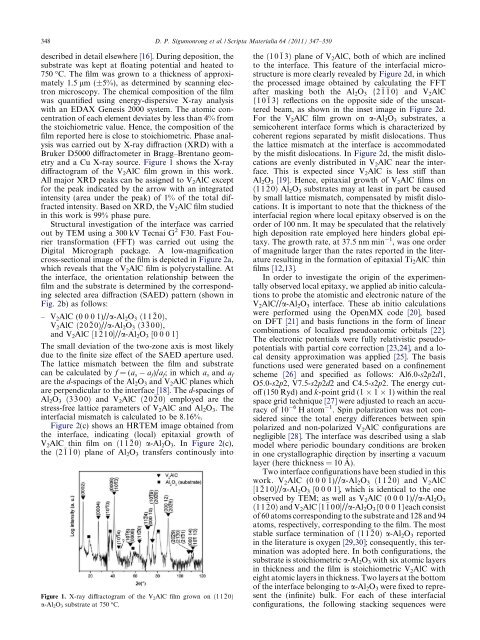
and a Cu X-ray source. Figure 1 shows the X-ray<br />
diffractogram <str<strong>on</strong>g>of</str<strong>on</strong>g> the <str<strong>on</strong>g>V2AlC</str<strong>on</strong>g> film grown in this work.<br />
All major XRD peaks can be assigned to <str<strong>on</strong>g>V2AlC</str<strong>on</strong>g> except<br />
for the peak indicated by the arrow with an integrated<br />
intensity (area under the peak) <str<strong>on</strong>g>of</str<strong>on</strong>g> 1% <str<strong>on</strong>g>of</str<strong>on</strong>g> the total diffracted<br />
intensity. Based <strong>on</strong> XRD, the <str<strong>on</strong>g>V2AlC</str<strong>on</strong>g> film studied<br />
in this work is 99% phase pure.<br />
Structural investigati<strong>on</strong> <str<strong>on</strong>g>of</str<strong>on</strong>g> the interface was carried<br />
out by TEM using a 300 kV Tecnai G 2 F30. Fast Fourier<br />
transformati<strong>on</strong> (FFT) was carried out using the<br />
Digital Micrograph package. A low-magnificati<strong>on</strong><br />
cross-secti<strong>on</strong>al image <str<strong>on</strong>g>of</str<strong>on</strong>g> the film is depicted in Figure 2a,<br />
which reveals that the <str<strong>on</strong>g>V2AlC</str<strong>on</strong>g> film is polycrystalline. At<br />
the interface, the orientati<strong>on</strong> relati<strong>on</strong>ship between the<br />
film and the substrate is determined by the corresp<strong>on</strong>ding<br />
selected area diffracti<strong>on</strong> (SAED) pattern (shown in<br />
Fig. 2b) as follows:<br />
– <str<strong>on</strong>g>V2AlC</str<strong>on</strong>g> (0 0 0 1)//a-Al2O3 ð1120Þ,<br />
<str<strong>on</strong>g>V2AlC</str<strong>on</strong>g> ð2020Þ//a-Al2O3 ð3300Þ,<br />
and <str<strong>on</strong>g>V2AlC</str<strong>on</strong>g> ½1210Š//a-Al2O3 [0001]<br />
The small deviati<strong>on</strong> <str<strong>on</strong>g>of</str<strong>on</strong>g> the two-z<strong>on</strong>e axis is most likely<br />
due to the finite size effect <str<strong>on</strong>g>of</str<strong>on</strong>g> the SAED aperture used.<br />
The lattice mismatch between the film and substrate<br />
can be calculated by f =(as af)/af; in which as and af<br />
are the d-spacings <str<strong>on</strong>g>of</str<strong>on</strong>g> the Al2O3 and <str<strong>on</strong>g>V2AlC</str<strong>on</strong>g> planes which<br />
are perpendicular to the interface [18]. The d-spacings <str<strong>on</strong>g>of</str<strong>on</strong>g><br />
Al2O3 ð3300Þ and <str<strong>on</strong>g>V2AlC</str<strong>on</strong>g> ð2020Þ employed are the<br />
stress-free lattice parameters <str<strong>on</strong>g>of</str<strong>on</strong>g> <str<strong>on</strong>g>V2AlC</str<strong>on</strong>g> and Al2O3. The<br />
interfacial mismatch is calculated to be 8.16%.<br />
Figure 2(c) shows an HRTEM image obtained from<br />
the interface, indicating (local) epitaxial growth <str<strong>on</strong>g>of</str<strong>on</strong>g><br />
<str<strong>on</strong>g>V2AlC</str<strong>on</strong>g> <str<strong>on</strong>g>thin</str<strong>on</strong>g> film <strong>on</strong> ð1120Þ a-Al2O3. In Figure 2(c),<br />
the ð2110Þ plane <str<strong>on</strong>g>of</str<strong>on</strong>g> Al2O3 transfers c<strong>on</strong>tinously into<br />
Figure 1. X-ray diffractogram <str<strong>on</strong>g>of</str<strong>on</strong>g> the V 2AlC film grown <strong>on</strong> ð1120Þ<br />
a-Al2O3 substrate at 750 °C.<br />
the ð1013Þ plane <str<strong>on</strong>g>of</str<strong>on</strong>g> <str<strong>on</strong>g>V2AlC</str<strong>on</strong>g>, both <str<strong>on</strong>g>of</str<strong>on</strong>g> which are inclined<br />
to the interface. This feature <str<strong>on</strong>g>of</str<strong>on</strong>g> the interfacial micro<str<strong>on</strong>g>structure</str<strong>on</strong>g><br />
is more clearly revealed by Figure 2d, in which<br />
the processed image obtained by calculating the FFT<br />
after masking both the Al2O3 {2110} and <str<strong>on</strong>g>V2AlC</str<strong>on</strong>g><br />
{1013} reflecti<strong>on</strong>s <strong>on</strong> the opposite side <str<strong>on</strong>g>of</str<strong>on</strong>g> the unscattered<br />
beam, as shown in the inset image in Figure 2d.<br />
For the <str<strong>on</strong>g>V2AlC</str<strong>on</strong>g> film grown <strong>on</strong> a-Al2O3 substrates, a<br />
semicoherent interface forms which is characterized by<br />
coherent regi<strong>on</strong>s separated by misfit dislocati<strong>on</strong>s. Thus<br />
the lattice mismatch at the interface is accommodated<br />
by the misfit dislocati<strong>on</strong>s. In Figure 2d, the misfit dislocati<strong>on</strong>s<br />
are evenly distributed in V 2AlC near the interface.<br />
This is expected since <str<strong>on</strong>g>V2AlC</str<strong>on</strong>g> is less stiff than<br />
Al2O3 [19]. Hence, epitaxial growth <str<strong>on</strong>g>of</str<strong>on</strong>g> <str<strong>on</strong>g>V2AlC</str<strong>on</strong>g> <str<strong>on</strong>g>films</str<strong>on</strong>g> <strong>on</strong><br />
ð1120Þ Al 2O 3 substrates may at least in part be caused<br />
by small lattice mismatch, compensated by misfit dislocati<strong>on</strong>s.<br />
It is important to note that the thickness <str<strong>on</strong>g>of</str<strong>on</strong>g> the<br />
interfacial regi<strong>on</strong> where local epitaxy observed is <strong>on</strong> the<br />
order <str<strong>on</strong>g>of</str<strong>on</strong>g> 100 nm. It may be speculated that the relatively<br />
high depositi<strong>on</strong> rate employed here hinders global epitaxy.<br />
The growth rate, at 37.5 nm min 1 , was <strong>on</strong>e order<br />
<str<strong>on</strong>g>of</str<strong>on</strong>g> magnitude larger than the rates reported in the literature<br />
resulting in the formati<strong>on</strong> <str<strong>on</strong>g>of</str<strong>on</strong>g> epitaxial Ti2AlC <str<strong>on</strong>g>thin</str<strong>on</strong>g><br />
<str<strong>on</strong>g>films</str<strong>on</strong>g> [12,13].<br />
In order to investigate the origin <str<strong>on</strong>g>of</str<strong>on</strong>g> the experimentally<br />
observed local epitaxy, we applied ab initio calculati<strong>on</strong>s<br />
to probe the atomistic and electr<strong>on</strong>ic nature <str<strong>on</strong>g>of</str<strong>on</strong>g> the<br />
V 2AlC//a-Al 2O 3 interface. These ab initio calculati<strong>on</strong>s<br />
were performed using the OpenMX code [20], based<br />
<strong>on</strong> DFT [21] and basis functi<strong>on</strong>s in the form <str<strong>on</strong>g>of</str<strong>on</strong>g> linear<br />
combinati<strong>on</strong>s <str<strong>on</strong>g>of</str<strong>on</strong>g> localized pseudoatomic orbitals [22].<br />
The electr<strong>on</strong>ic potentials were fully relativistic pseudopotentials<br />
with partial core correcti<strong>on</strong> [23,24], and a local<br />
density approximati<strong>on</strong> was applied [25]. The basis<br />
functi<strong>on</strong>s used were generated based <strong>on</strong> a c<strong>on</strong>finement<br />
scheme [26] and specified as follows: Al6.0-s2p2d1,<br />
O5.0-s2p2, V7.5-s2p2d2 and C4.5-s2p2. The energy cut<str<strong>on</strong>g>of</str<strong>on</strong>g>f<br />
(150 Ryd) and k-point grid (1 1 1) wi<str<strong>on</strong>g>thin</str<strong>on</strong>g> the real<br />
space grid technique [27] were adjusted to reach an accuracy<br />
<str<strong>on</strong>g>of</str<strong>on</strong>g> 10 6 H atom 1 . Spin polarizati<strong>on</strong> was not c<strong>on</strong>sidered<br />
since the total energy differences between spin<br />
polarized and n<strong>on</strong>-polarized <str<strong>on</strong>g>V2AlC</str<strong>on</strong>g> c<strong>on</strong>figurati<strong>on</strong>s are<br />
negligible [28]. The interface was described using a slab<br />
model where periodic boundary c<strong>on</strong>diti<strong>on</strong>s are broken<br />
in <strong>on</strong>e crystallographic directi<strong>on</strong> by inserting a vacuum<br />
layer (here thickness = 10 A ˚ ).<br />
Two interface c<strong>on</strong>figurati<strong>on</strong>s have been studied in this<br />
work. V 2AlC (0001)//a-Al 2O 3 ð1120Þ and V 2AlC<br />
½1210Š//a-Al2O3 [0 0 0 1], which is identical to the <strong>on</strong>e<br />
observed by TEM; as well as <str<strong>on</strong>g>V2AlC</str<strong>on</strong>g> (0 0 0 1)//a-Al2O3<br />
ð1120Þ and V 2AlC ½1100Š//a-Al 2O 3 [0 0 0 1] each c<strong>on</strong>sist<br />
<str<strong>on</strong>g>of</str<strong>on</strong>g> 60 atoms corresp<strong>on</strong>ding to the substrate and 128 and 94<br />
atoms, respectively, corresp<strong>on</strong>ding to the film. The most<br />
stable surface terminati<strong>on</strong> <str<strong>on</strong>g>of</str<strong>on</strong>g> ð1120Þ a-Al 2O 3 reported<br />
in the literature is oxygen [29,30]; c<strong>on</strong>sequently, this terminati<strong>on</strong><br />
was adopted here. In both c<strong>on</strong>figurati<strong>on</strong>s, the<br />
substrate is stoichiometric a-Al2O3 with six atomic layers<br />
in thickness and the film is stoichiometric V 2AlC with<br />
eight atomic layers in thickness. Two layers at the bottom<br />
<str<strong>on</strong>g>of</str<strong>on</strong>g> the interface bel<strong>on</strong>ging to a-Al2O3 were fixed to represent<br />
the (infinite) bulk. For each <str<strong>on</strong>g>of</str<strong>on</strong>g> these interfacial<br />
c<strong>on</strong>figurati<strong>on</strong>s, the following stacking sequences were