President's Corner (cont.) - American Association for Crystal Growth
President's Corner (cont.) - American Association for Crystal Growth
President's Corner (cont.) - American Association for Crystal Growth

Create successful ePaper yourself
Turn your PDF publications into a flip-book with our unique Google optimized e-Paper software.
<strong>American</strong> <strong>Association</strong> <strong>for</strong> <strong>Crystal</strong> <strong>Growth</strong><br />
Winter 2013 Vol. 38, Issue 1
GROWING CRYSTALS ?<br />
CZ or Bridgeman. Resistance or Induction. Vertical or<br />
Horizontal. ZIRCAR Ceramics, Inc. works hard <strong>for</strong> you<br />
Precision CNC machined growth chamber thermal<br />
insulation in Al2O3, ZrO2 and many other compositions<br />
We Can Help Call Today<br />
The low-mass thermal insulation products<br />
offered by ZIRCAR Ceramics, Inc., have<br />
been helping crystal growers obtain high<br />
yields of quality crystals <strong>for</strong> more than<br />
35 years.<br />
Specializing in CNC-machined ZrO2,<br />
Al2O3, Al2O3-SiO2 fiber products and<br />
Microporous thermal insulation. MoSi2<br />
and resistance wire heating elements.<br />
Resistance wire heating elements <strong>for</strong> growth and<br />
annealling systems with temperatures to 1300C<br />
Vacuum <strong>for</strong>med ceramic fiber and microporous insulation<br />
<strong>for</strong> effective management of system energy issues<br />
e-mail: dph@zircarceramics.com<br />
Tel: 1 845 651 6600 ext 13<br />
www.zircarceramics.com
EDITOR<br />
Candace Lynch<br />
Inrad Optics<br />
clynch@inradoptics.com<br />
201-767-1910 x 583<br />
ADVERTISING EDITOR<br />
David Bliss<br />
dfbliss@gmail.com<br />
DESIGN & LAYOUT<br />
Shoshana Nash<br />
aacg@comcast.net<br />
303-539-6907<br />
Volume 38, Issue 1 Winter 2013<br />
5 President’s <strong>Corner</strong><br />
7 ACCGE/West Review<br />
8 Interview with Lodewijk van den Berg<br />
12 Advanced Photonic <strong>Crystal</strong>s Profile<br />
14 Come to Keystone<br />
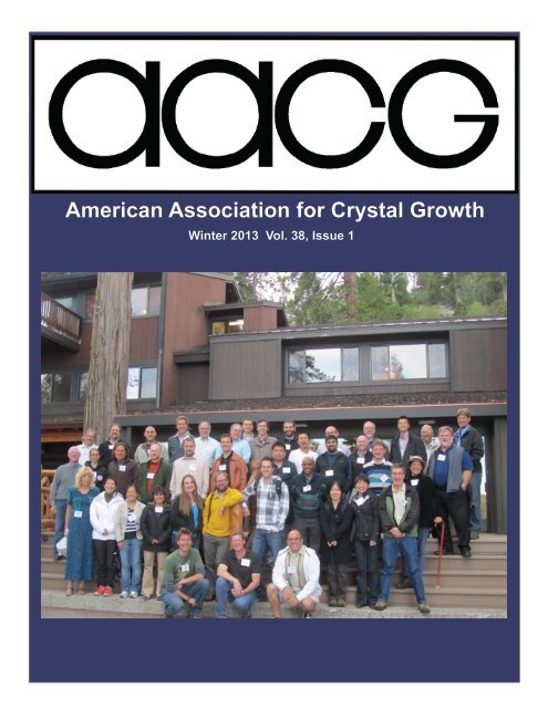
On the cover:<br />
Group photo taken at the 23rd ACCGE/West meeting<br />
in Fallen Leaf Lake, CA. All ACCGE/West<br />
photos are courtesy of David Kisailus.<br />
To opt out of receiving the newsletter, please email<br />
aacg@comcast.net, subject: newsletter opt out.<br />
AACG newsletter<br />
AACG OFFICERS<br />
PRESIDENT<br />
Peter Schunemann<br />
BAE Systems<br />
VICE PRESIDENT<br />
Robert Biefeld<br />
Sandia National Laboratory<br />
TREASURER<br />
Dave Vanderwater<br />
Philips-Lumileds Lighting<br />
SECRETARY<br />
Joan Redwing<br />
Pennsylvania State University<br />
SECTION PRESIDENTS<br />
WEST<br />
Edith Bourret-Courchesne<br />
Lawrence Berkeley Laboratory<br />
MID-ATLANTIC<br />
Glen Kowach<br />
The City University of New York<br />
CAPITAL<br />
Ronald G. Rosemeier<br />
Brimrose<br />
NEW ENGLAND<br />
David Bliss<br />
Air Force Research Laboratory<br />
AACG EXECUTIVE ADMINISTRATOR<br />
Shoshana Nash<br />
6986 S. Wadsworth Court, Littleton, CO 80128<br />
303-539-6907 and 888-506-1271 (toll-free)<br />
303-482-2775 (fax)<br />
AACG@comcast.net<br />
AACG Newsletter Winter 2013 3
4<br />
AACG Corporate Supporters<br />
AIXTRON<br />
www.aixtron.com<br />
Dr. Christof Sommerhalter<br />
c.sommerhalter@aixtron.com<br />
(847) 215-7335 ext. 1351<br />
AKZO Nobel High Purity Metalorganics<br />
www.akzonobel.com<br />
Taeho Ko<br />
taeho.ko@akzonobel.com<br />
(281) 817-9222<br />
<strong>American</strong> <strong>Crystal</strong> Technology<br />
www.axt.com<br />
Lisa Tan<br />
ltan@axt.com<br />
(510) 438-4707<br />
Coherent Advanced <strong>Crystal</strong> Group<br />
www.coherentinc.com<br />
Dominic Loiacono<br />
dominic.loiacono@coherentinc.com<br />
(973) 581-1717<br />
Dow Electric Materials<br />
www.dowelectronicmaterials.com<br />
Michele Davison<br />
mdavison@rohmhaas.com<br />
(978) 557-1837<br />
Heraeus Materials Technology<br />
www.heraeus.com<br />
John Lazzari<br />
john.lazzari@heraeus.com<br />
(201) 647-8672<br />
Fairfield <strong>Crystal</strong><br />
www.fairfieldcrystal.com<br />
Andy Timmerman<br />
swang@fairfieldcrystal.com<br />
Johnson Matthey<br />
www.noble.matthey.com<br />
Bob Staargaard<br />
staarrl@jmusa.com<br />
(610) 648-8443<br />
LayTec Gmbh<br />
www.laytec.de<br />
Dr. Elizabeth Steimetz<br />
steimetz@lyatec.de<br />
49-30-3980-0800<br />
Northrop Grumman<br />
www.northropgrumman.com<br />
David Kahler<br />
david.kahler@ngc.com<br />
Photonic Science<br />
www.photonic-science.com<br />
Diane Brau<br />
kelly@photonic-science.co.uk<br />
+44(0)1580<br />
ProChem<br />
www.prochemonline.com<br />
Reno Novak<br />
prochem1@aol.com<br />
(815) 398-1788<br />
SAFC Hitech<br />
www.safcglobal.com<br />
Sarah Leese<br />
sarah.leese@sial.com<br />
Thermcraft, Inc.<br />
www.thermcraftinc.com<br />
Tom Crafton<br />
t.crafton@thermcraftinc.com<br />
(336) 784-4800<br />
Veeco Instruments Inc.<br />
www.veeco.com<br />
Fran Brennan<br />
fbrennen@veeco.com<br />
Zircar Ceramics, Inc.<br />
www.zircarceramics.com<br />
David Hamling<br />
dph@zircarceramics.com<br />
(845) 651-6600 ext. 13<br />
Zircar Zirconia, Inc.<br />
www.zircarzirconia.com<br />
David Hoskins<br />
sales@zircarzirconia.com<br />
(845) 651-3040 ext. 37<br />
AACG Newsletter Winter 2013
President’s <strong>Corner</strong><br />
Community. It’s what the <strong>American</strong> <strong>Association</strong> of <strong>Crystal</strong><br />
<strong>Growth</strong> is all about.<br />
An experience this summer really highlighted the power<br />
of community and the networking opportunities that come<br />
from being a member of the AACG. Back on July 2nd<br />
Vince Fratello (a <strong>for</strong>mer AACG president and still the<br />
heart and soul of the organization) <strong>for</strong>warded a request<br />
from Roger Route at Stan<strong>for</strong>d (another long time member)<br />
looking <strong>for</strong> a <strong>cont</strong>act in the Float Zone silicon industry to<br />
help him find a reliable source of ultra-low-loss silicon<br />
<strong>for</strong> use as a test mass in the LIGO project (The Laser Interferometer<br />
Gravitational-Wave Observatory). I replied<br />
that I thought Ted Ciszek, Dave Witter, or Peter Rudolph<br />
would know the best people to <strong>cont</strong>act and I <strong>for</strong>warded<br />
the request to them. Peter Rudolph (recently retired from<br />
IKZ in Berlin and <strong>for</strong>mer president of the German <strong>Association</strong><br />
<strong>for</strong> <strong>Crystal</strong> <strong>Growth</strong> - DGKK) quickly replied with<br />
the names and <strong>cont</strong>act in<strong>for</strong>mation of two key experts in<br />
this technology – Dr. H. Riemann (from IKZ Berlin) and<br />
Dr. Wilfried Ammon (who was employed at Siltronic AG<br />
- <strong>for</strong>merly Wacker Siltronic) as well as the name and website<br />
of Topsil in Denmark, an important FZ Si producer in<br />
Europe. Ted Ciszek replied shortly thereafter confirming<br />
Peter’s suggestions as the best possible leads and added<br />
Shinetsu Handotai, a Japanese company with a US sales<br />
office, as another option worth considering. Finally Dave<br />
Witter replied with a more technical response, pointing out<br />
that years ago Texas Instruments had developed an inverted<br />
float zone process <strong>for</strong> growing ultra-high resistivity silicon<br />
(30,000 ohm-centimeters) that probably had the extremely<br />
low infrared absorption losses that Roger was looking <strong>for</strong>.<br />
He even still had a sample of this material in case Roger<br />
wanted to make some measurements.<br />
So within a matter of hours Roger had a direct line to the<br />
best sources in the world to help his project succeed, and<br />
all by sending a single email! It’s amazing how quickly you<br />
can get at the heart of a problem when you know the right<br />
people to talk to, particularly in a highly specialized field<br />
such as crystal growth. (In the wake of this event, I very<br />
naturally suggested that Roger should renew his AACG<br />
membership, which had recently expired, by clicking on<br />
the membership link at http://www.crystalgrowth.org/ or<br />
AACG president Peter Schunemann<br />
<strong>cont</strong>acting Shoshana Nash directly at aacg@comcast.<br />
net. He is now happily a member in good standing once<br />
again.)<br />
My faith in the crystal growth community was also refreshed<br />
when I attended the ACCGE/West Meeting from<br />
June 3-6 at Stan<strong>for</strong>d Sierra Camp in Fallen Leaf Lake,<br />
CA. Despite more than two decades of membership in<br />
the AACG, I had never be<strong>for</strong>e attended the West Coast<br />
Meeting, and I was greatly rewarded <strong>for</strong> finally doing so<br />
(Vince, an even more ancient AACG member, was also<br />
there <strong>for</strong> the first time, having recently migrated from<br />
Integrated Photonics in New Jersey to Quest Integrated<br />
Inc. in Kent, Washington). ACCGE/West is a delightful<br />
meeting, and one of the best kept secrets in crystal growth<br />
(which is saying a lot, given the propensity of crystal<br />
growers <strong>for</strong> keeping secrets!). The scenery was spectacular,<br />
and the venue homey and relaxing. When I drove into<br />
Stan<strong>for</strong>d Sierra Camp it felt more like summer camp than<br />
a scientific conference. The rustic wooden cabins were<br />
far more com<strong>for</strong>table and nicely furnished than the places<br />
I went as a kid, however, and when I entered the main<br />
lodge I found that instead of singing Kum Ba Yah the other<br />
“campers” were riveted by an exceptional plenary talk<br />
being given by Linda Sapochak (Program Director, Solid<br />
State and Materials Chemistry) from NSF. The evening<br />
<strong>cont</strong>inued with another excellent plenary talk by Hanchen<br />
Huang from the University of Connecticut, followed by<br />
free beer and wine and engaging scientific discussions in<br />
front of the fireplace. (Dave Vanderwater, our esteemed<br />
AACG Newsletter Winter 2013 5
treasurer, attended the meeting as always, and having assured<br />
the meeting was in the black authorized free beer<br />
and wine EVERY evening as well as during dinner and<br />
the poster session.) The rest of the conference over the<br />
next two and a half days was equally stimulating – with<br />
talks scheduled in the mornings and evenings around free<br />
afternoons perfect <strong>for</strong> hiking and getting to know fellow<br />
crystal growers. The single session <strong>for</strong>mat and the broad<br />
range of topics made <strong>for</strong> lively discussion and questions<br />
from experts and novices alike. My congratulations to<br />
Sean Hearne (Conference Chair), Luis Zepada-Ruiz, and<br />
David Kisailus (Program Chairs) <strong>for</strong> organizing a highly<br />
successful meeting.<br />
An occasional kind word from our colleagues is another<br />
benefit of being active in our community. I got a very<br />
nice email from one of our members this summer regarding<br />
the newsletter:<br />
Dear Peter:<br />
I wanted to complement you on the AACG newsletter, it<br />
6<br />
President’s <strong>Corner</strong> (<strong>cont</strong>.)<br />
was just a great, in<strong>for</strong>mative issue. I especially liked your<br />
Presidents <strong>Corner</strong> and David Bliss’s interview of Bruce<br />
Chai. Bravo and happy 4th of July.<br />
Sincerely,<br />
David Hoskins<br />
Sales Manager<br />
Zircar Zirconia, Inc<br />
Thank you, David, <strong>for</strong> your encouragement, but it is really<br />
Candace Lynch at Inrad Optics and Shoshana Nash, our<br />
Administrator at AACG Headquarters in Littleton, CO (as<br />
well as all those who <strong>cont</strong>ributed <strong>cont</strong>ent) who should be<br />
thanked <strong>for</strong> their dedicated ef<strong>for</strong>ts on the last newsletter,<br />
and <strong>for</strong> getting another one out to you so quickly. I hope<br />
you all enjoy the great <strong>cont</strong>ent in this issue as well.<br />
In your service,<br />
Pete Schunemann<br />
AACG President<br />
Complete X-ray Laue camera system replaces Polaroid film<br />
Digital Laue detectors – an alternative to high sensitivity films<br />
<strong>for</strong> both laboratories and synchrotrons wishing to carry out systematic bulk crystal orientation and micro crystal characterisation.<br />
The cameras allow unique back scattered geometry with<br />
collection time varying from near real time to a few minutes,<br />
depending on source, detector and crystal combination.<br />
Automated sample rotation, combined with shutterless<br />
acquisition brings simpler and more flexible data collection<br />
routines.<br />
The acquisition software delivers ready to be indexed digital<br />
images from PC, to Linux remote <strong>cont</strong>rolled machines.<br />
Indexation of Laue patterns can be per<strong>for</strong>med off line using<br />
dedicated software packages.<br />
An existing Laue set up can be upgraded with turnkey solution<br />
including beam delivery: i.e. X-ray source, collimators,<br />
goniometer/sample holder up to system installation/integration.<br />
Very high resolution detectors allowing strain analysis studies<br />
are available on demand.<br />
Laue system<br />
W111 pattern acquired with<br />
standard 04x08mm Cu<br />
source using 25kV, 25mA<br />
and 5 minutes exposure.<br />
Images courtesy SPL, Netherlands<br />
Contact<br />
Daniel BRAU Sales & Marketing Director - Photonic Science Limited Email : Info@photonic-science.com<br />
Tel : +33 (0) 4 76 93 57 20 Fax : +33 (0) 4 76 93 57 22 Web Site http://www.photonic-science.com<br />
AACG Newsletter Winter 2013
The Western Section of the <strong>American</strong> <strong>Association</strong> <strong>for</strong> <strong>Crystal</strong><br />
<strong>Growth</strong> hosted the 23rd <strong>American</strong> Conference on <strong>Crystal</strong><br />
<strong>Growth</strong> and Epitaxy–West (ACCGE/West) from June<br />
3-6, 2012, at the Stan<strong>for</strong>d Sierra Camp, Fallen Leaf Lake,<br />
CA. Sean Hearne of Sandia National Laboratory served<br />
as the Conference Chair, with Program Co-Chairs of Luis<br />
Zepeda-Ruiz (Lawrence Livermore National Laboratory)<br />
and David Kisailus (University of Cali<strong>for</strong>nia Riverside).<br />
There were a total of 53 paid attendees, with 5 guests, comprising<br />
a small but engaging group of devotees to the wonders<br />
of crystal growth.<br />
As so often occurs during springtime in the Sierra Nevada,<br />
the weather fluctuated wildly from summer, warm and sunny,<br />
to winter, cold and snowy, then back to spring, brisk but<br />
clear. Program Co-Chair Kisailus demonstrates the effects<br />
of these three seasons within three days in the accompanying<br />
photo.<br />
Figure 2: James DeYoreo (LBNL) presents an<br />
overview of his research during a cozy evening<br />
session featuring a crackling fire in the<br />
Sierra Camp Lodge.<br />
The technical program was led off on Sunday evening by<br />
Dr. Linda Sapochak, who gave a broad and captivating plenary<br />
talk entitled, “The Good, the Bad and the Beautiful:<br />
The Relevance of <strong>Crystal</strong>line Material Research to Advancing<br />
Materials Discovery and Development.” Sapochak<br />
leads the Solid State and Materials Chemistry program at<br />
the National Science Foundation and spoke about the increased<br />
emphasis on crystal growth research at NSF, motivated<br />
in part by the recent Materials Genome Initiative<br />
and the 2009 NRC report, “Frontiers in <strong>Crystal</strong>line Matter:<br />
From Discovery to Technology.”<br />
ACCGE/West Review<br />
Figure 1: If this is June in the Sierra Nevada, what<br />
is the appropriate attire <strong>for</strong> ACCGE/West?<br />
During the next days, technical sessions on “Fundamentals<br />
of Materials <strong>Growth</strong>,” “Biomaterials <strong>Growth</strong> and Processes,”<br />
and “Energy Materials <strong>Growth</strong> and Applications”<br />
featured a wide array of presentations, delivered by researchers<br />
ranging from established professionals to graduate<br />
students. Per the historical conduct of this conference,<br />
sessions featured many invited talks from research leaders<br />
who presented a broader perspective of their work, thus<br />
engaging attendees from all backgrounds. Technical sessions<br />
were held in mornings and evenings, allowing afternoon<br />
breaks to further engage conference participants<br />
in social activities, such as hikes along the beautiful trails<br />
from the camp. A poster session, held in conjunction with<br />
wine tasting and appetizers, featured other research, especially<br />
projects carried out by graduate students. Common<br />
meals, prepared and served with uncommon skill by camp<br />
personnel, and the open bar after the evening sessions also<br />
added to the intimate, workshop-like experience of the<br />
conference.<br />
The conference concluded at lunch on Wednesday, after<br />
three days of haphazard weather that surrounded high-level<br />
and enlightening discussions about crystal growth. The<br />
24th ACCGE/West conference will be chaired by David<br />
Kisailus (david@engr.ucr.edu) and will be held at, as all<br />
prior meetings, the stunning Stan<strong>for</strong>d Sierra Camp, from<br />
June 8-11, 2014.<br />
For more in<strong>for</strong>mation, please refer to the AACG website at<br />
www.crystalgrowth.org.<br />
AACG Newsletter Winter 2013 7
8<br />
Interview with Lodewijk van den Berg<br />
During the 1980s many AACG members were actively<br />
involved in the Space Program at NASA, studying the<br />
effects of crystal growth processes under microgravity<br />
conditions. Spacelab was a reusable laboratory that<br />
flew on the Space Shuttle, allowing scientists to per<strong>for</strong>m<br />
experiments in microgravity while in Earth orbit. The<br />
program <strong>cont</strong>ributed greatly to the scientific understanding<br />
of crystal growth, and resulted in innovations to<br />
the technology, notably the detached Bridgman growth<br />
technique. Recently, David Bliss spoke with one AACG’s<br />
most celebrated astronauts, Lodewijk van den Berg, about<br />
his life experience in crystal growth and his time as an<br />
astronaut in the NASA Spacelab program.<br />
DB: How did you first get started in crystal growth?<br />
LB: My first start in crystal growth was at the University<br />
of Delaware. I started by growing a metallic alloy<br />
<strong>for</strong> a professor who needed a few rods of nickel alloy <strong>for</strong><br />
teaching his class. It was a horizontal Bridgman process<br />
in a closed tube.<br />
DB: Was that the first university you attended?<br />
LB: No, be<strong>for</strong>e that, I started in the 1950s at the Technical<br />
University of Delft in the Netherlands in chemical engineering,<br />
and when I graduated, I was supposed to disappear<br />
into the oil industry, to a place like Royal Dutch Shell. But<br />
my adviser told me: “You are too young <strong>for</strong> a regular job. I<br />
have a friend in Delaware who owes me a favor, and he will<br />
give you financial support at the University.” Two months<br />
later we got an answer back: “Sure, we will be glad to have<br />
him, send him over”.<br />
I arrived in the middle of the fall semester, and I had to<br />
jump into classes while also working on the grant. In the<br />
second year Professor Karl Boer in the Physics department<br />
heard about my work on the alloy crystals and he was interested<br />
in cadmium sulfide crystals <strong>for</strong> solar cells. But the<br />
physicists knew nothing about materials or crystal growth,<br />
and I had to start from scratch.<br />
DB: How do you grow CdS crystals from the vapor?<br />
LB: I designed the furnace and built the temperature <strong>cont</strong>rollers<br />
<strong>for</strong> the right gradients and so <strong>for</strong>th. It was an open<br />
tube, a boat with CdS powder, a temperature gradient and<br />
Contributed by David Bliss<br />
Van den Berg with crystal grown in space.<br />
crystal growth in the cool zone. A constant flow of nitrogen<br />
through the tube provided the transport to the colder<br />
end. Then I modified it to add hydrogen sulfide gas in order<br />
to maintain the stoichiometry of the CdS crystals, and<br />
of course this gas had to be burned at the outlet. Strictly<br />
chemical engineering work.<br />
DB: Was that the subject of your master’s thesis?<br />
LB: Yes, and the grant went well, so the university had to<br />
arrange an extension <strong>for</strong> me to stay in the US <strong>for</strong> a longer<br />
time. The University said: “Now that you have your master’s<br />
degree, we want you to go <strong>for</strong> a PhD, so that you can<br />
stay here and grow these crystals.”<br />
They had a new program that they called applied science.<br />
It was a combination of chemical engineering, materials<br />
science, and physics. Originally, I was supposed to<br />
specialize in one discipline, but I ended up by taking<br />
the exams in all three areas. It took me more than eight<br />
years. At that time the DuPont company was building a<br />
AACG Newsletter Winter 2013
nylon and Dacron factory in Germany. They requested<br />
the University to provide someone who could translate<br />
their drawings from English to German, and translate the<br />
regulations from German to English. Dutchmen know<br />
German pretty well, so I was delegated by the physics<br />
department to do this. Very interesting work, given my<br />
chemical engineering background, but it did slow down<br />
the work <strong>for</strong> the degree.<br />
DB: Did you consider going back to the Netherlands<br />
after university?<br />
LB: Well, I finally finished the PhD, and I met an <strong>American</strong><br />
girl. We soon got married, but she didn’t want to go<br />
to live in Europe. So I applied <strong>for</strong> citizenship and soon<br />
found a job at EG&G at their laboratory in Santa Barbara,<br />
where they needed a crystal grower to grow mercuric<br />
iodide crystals. At that time their main consultant<br />
was none other than Professor Michael Schieber from the<br />
Hebrew University in Jerusalem. When I showed him<br />
the crystals I had grown, he was excited and insisted that<br />
I come to EG&G. I would need to have citizenship, but<br />
with help from EG&G my papers came through in six<br />
months.<br />
DB: Did you develop a new crystal growth process at<br />
EG&G?<br />
LB: I found that the biggest problem was preparation of<br />
the materials <strong>for</strong> crystal growth. You have to start with<br />
highly pure materials. I think this is a common problem<br />
you see in the literature. It is clear that many times the<br />
starting material is not pure enough to get high quality<br />
crystals. So the group that I worked with designed new<br />
furnaces to purify and grow HgI 2 <strong>for</strong> nuclear radiation<br />
detectors.<br />
DB: Where were you when they approached you to become<br />
an astronaut <strong>for</strong> NASA?<br />
LB: That was when I worked at EG&G in Santa Barbara,<br />
in the early 1980’s. NASA had decided that with<br />
the new shuttle, they needed good crystal growth experiments<br />
<strong>for</strong> the SpaceLab. So we put in a proposal, not<br />
thinking we would be selected, and we were very surprised<br />
that NASA came back and accepted our proposal.<br />
Of course, NASA was very interested in studying fluid<br />
dynamics, inspired partly by Rosenberger, so we designed<br />
a crystal growth system that could be used in space under<br />
low-gravity conditions. But when the operations group<br />
in Houston looked at the design and procedures of the experiment,<br />
they decided they could not train in two years<br />
one of their astronauts to become a full-fledged crystal<br />
Moving around in the Spacelab.<br />
grower. Instead NASA requested a group of volunteers<br />
from the scientific community to be trained as astronauts.<br />
NASA established an investigators’ working group, with<br />
my boss Wayne Schnepple as the head.<br />
He received a letter requesting a list of 16 names of people<br />
who would like to do this job of growing crystals in<br />
space. He asked me “How do we find 16 guys who are<br />
willing to do this?” We sent letters to all members of the<br />
AACG asking <strong>for</strong> volunteers to be trained as an astronaut<br />
<strong>for</strong> Spacelab 3. Out of that we received only 15 credible<br />
answers, because not many people want to do this, as it<br />
turns out. You have to sacrifice about two years from<br />
your career, not to mention the strain on your family.<br />
So Wayne said to me “We have to make a good impression<br />
on NASA, so why not put your name on the list as<br />
the 16th volunteer?” Of course I had poor eyes, and a<br />
lot of other little problems, so I agreed, knowing that on<br />
the first round of selection, I would be ruled out. Then,<br />
based on educational backgrounds, NASA whittled the<br />
list down to eight acceptable individuals. After that, the<br />
science PI’s on the Spacelab 3 program were to select<br />
the four most qualified to do the experiments. I was still<br />
on the list, because I had quite a few years of experience<br />
growing crystals. At that point, it was too late <strong>for</strong> me to<br />
say “No, I don’t really want to do this.” Wayne said, “<br />
The next step will be the NASA physical, and there you<br />
definitely will wash out. So don’t worry.”<br />
So seven of us men and one woman went <strong>for</strong> a threeday<br />
intensive physical at NASA. From 7:30 am to 4:30<br />
pm you never stop, except <strong>for</strong> a half-hour lunch. At the<br />
clinic, a nurse takes many blood samples from you and<br />
escorts you from one test station to another. This is after<br />
fasting <strong>for</strong> 24 hours. If you can take that <strong>for</strong> three days,<br />
AACG Newsletter Winter 2013 9
Interview with Lodewijk van den Berg (<strong>cont</strong>.)<br />
NASA will tell you that was a very good test we put you<br />
through to see how you could handle this deprivation. In<br />
the end I was one of the four selected to participate in operating<br />
the experiments planned <strong>for</strong> Spacelab 3.<br />
DB: How old were you when you were selected?<br />
LB: I was 53 years old. After we had been training <strong>for</strong><br />
about two years, NASA selected the primes and the backups.<br />
I was selected as one of the primes! So I had to go<br />
- end of story!<br />
DB: What was the training like?<br />
LB: There were two kinds of training, scientific and<br />
shuttle systems. We were trained to per<strong>for</strong>m basic operations<br />
of most of the 15 experiments on board. So we visited<br />
the laboratories of the PI’s to learn how to run their<br />
experiments. This was a very interesting experience, because<br />
how many crystal growers ever learn, <strong>for</strong> example,<br />
how to take photographs of the Magellan nebula, to take<br />
care of laboratory rats and monkeys, and to per<strong>for</strong>m autogenic<br />
biofeedback so that you can <strong>cont</strong>rol your heart rate,<br />
blood flow and blood pressure with the power of your<br />
own mind?<br />
The other side of it was astronaut training, and that was<br />
like going back to graduate school. We had to study, and<br />
practice, about twenty 70-page manuals <strong>for</strong> operation of<br />
the various shuttle systems covering safety, fire suppression,<br />
communication, food preparation, use of the bathroom<br />
system, and so <strong>for</strong>th.<br />
DB: When you came back from space, did you still have<br />
a job at EG&G?<br />
LB: Yes, that was in 1985, and I <strong>cont</strong>inued at EG&G<br />
until they closed in 1995. When EG&G eventually disbanded,<br />
Carl Rester of Constellation Technology in Florida<br />
bought the mercuric iodide laboratory. He moved everything,<br />
including me, and installed us in a <strong>for</strong>mer DoE<br />
facility. Vapor growth at low temperatures is nice because<br />
you can observe the process, but if you want to get large<br />
volume crystals, it is difficult because of the slow growth<br />
rate. You can’t grow these crystals from the melt, because<br />
they have a temperature dependent change in structure<br />
when they cool down.<br />
Another problem with melt growth of compounds is every<br />
time you heat them up, you have some degree of dissocia-<br />
10<br />
Operating HgI 2 crystal growth system in Spacelab.<br />
tion, and when they cool down, you have a stoichiometry<br />
problem. Vapor growth at lower temperatures is a better<br />
way, if you can find a large-scale process that is efficient<br />
and cost-effective.<br />
DB: And what happened to the HgI 2 growth ef<strong>for</strong>t?<br />
LB: About two years ago, the government stopped supporting<br />
the crystal growth ef<strong>for</strong>t at Constellation. I decided<br />
to retire then. Most of the equipment has been<br />
moved to RMD in Watertown, Massachusetts, <strong>for</strong> potential<br />
future use in growth of other detectors with high<br />
energy resolution at room temperature, like Thallium<br />
Bromide.<br />
DB: Finally, what would be your advice to future crystal<br />
growers?<br />
LB: The first thing is kind of emotional. If you like to<br />
do crystal growth, then go <strong>for</strong> it! But it won’t make you<br />
rich.<br />
On the whole, I see less demand <strong>for</strong> large single crystals.<br />
Most of the money is in thin films. But remember, even<br />
epitaxial growth requires a substrate, and that means single<br />
crystals, with issues like surface activity, homogeneity,<br />
and defect <strong>cont</strong>rol – all the bread and butter of bulk<br />
crystal growth. As a research field, I think that growth<br />
of sizable single crystals is still the only way to learn the<br />
fundamental properties of new compounds.<br />
AACG Newsletter Winter 2013
February 2-7, 2013<br />
SPIE Photonics West<br />
San Francisco, CA<br />
http://spie.org/x2584.xml<br />
March 3-7, 2013<br />
TMS 2013<br />
San Antonio, TX<br />
http://www.tms.org/meetings/annual13/AM-<br />
13home.aspx<br />
April 29-Mary 3, 2013<br />
SPIE Defense, Security, and Sensing 2013<br />
Baltimore, MD<br />
http://spie.org/defense-security-sensing.xml<br />
May 13-16, 2013<br />
CS MANTECH<br />
New Orleans, LA<br />
http://www.csmantech.org/index.html<br />
Upcoming Events<br />
July 21-26, 2013<br />
The 19th <strong>American</strong> Conference on <strong>Crystal</strong> <strong>Growth</strong> and<br />
Epitaxy & 16th Biennial Workshop on Organometallic<br />
Vapor Phase Epitaxy<br />
Keystone, CO<br />
http://www.crystalgrowth.org/AACGE-19.html<br />
August 11-16, 2013<br />
17th International Conference on <strong>Crystal</strong> <strong>Growth</strong> and<br />
Epitaxy<br />
Warsaw, Poland<br />
http://science24.com/event/iccge17/<br />
July 13-18, 2014<br />
ICMOVPE XVII<br />
Lausanne, Switzerland<br />
GROWTH STATION INSULATION!<br />
Custom Made Zirconia or Alumina<br />
Visit www.zircarzirconia.com<br />
or call (845) 651–3040<br />
Please submit conference in<strong>for</strong>mation to the editor <strong>for</strong><br />
inclusion in future issues.<br />
AACG Newsletter Winter 2013 11
Corporate Profile<br />
12<br />
Advanced Photonic <strong>Crystal</strong>s<br />
Advanced Photonic <strong>Crystal</strong>s (APC) was established in<br />
2002 as a spin-out from Clemson University by Dr. John<br />
J. Egan (CEO). APC’s mission is the production of superior<br />
single crystal optical materials via an advanced low<br />
temperature hydrothermal growth (HTG) process. From<br />
its inception, the company has worked closely with Dr.<br />
Joseph W. Kolis (Clemson) and has licensed a number of<br />
technologies from Clemson related to optical crystals and<br />
hydrothermal growth methods. One of Dr. Kolis’ <strong>for</strong>mer<br />
students, Dr. Henry G. Giesber III, is now a principal scientist<br />
at APC and was largely responsible <strong>for</strong> the R&D<br />
critical to the success of those technologies.<br />
All materials produced at APC are grown hydrothermally.<br />
HTG uses elevated temperatures and pressures to produce<br />
bulk crystals from solution. A thermal gradient generates<br />
a saturated solution in the feedstock region (hotter<br />
zone) and a supersaturated region in the cooler growth<br />
zone where the seed crystal is located (Figure 1). HTG<br />
at APC is per<strong>for</strong>med in modified Morey-type autoclaves<br />
lined with precious metals (Au or Pt). While Morey au-<br />
Contributed by Henry G. Giesber III<br />
Figure 1. Schematic of typical hydrothermal autoclave with temperature gradient.<br />
Ref: C. D. McMillen and J. W. Kolis Philosophical Magazine 92 (2012) 2686.<br />
toclaves can <strong>cont</strong>ain pressures of approximately 10,000<br />
psi at 450 °C, APC’s modified autoclaves can <strong>cont</strong>ain up<br />
to 60,000 psi at 700 °C. Current autoclaves in use have<br />
internal volumes of 400 ml and 1600 ml, with volumes up<br />
to 10 L anticipated in the future.<br />
The relatively low temperatures used <strong>for</strong> HTG can result<br />
in reduced thermal strain and impurity <strong>cont</strong>amination<br />
relative to crystals produced by traditional melt methods.<br />
For example, lutetium oxide (Lu 2 O 3 ) has an extremely<br />
high melting point of approximately 2500 °C. Using<br />
chemical know-how, the scientists at APC have grown<br />
this material below 650 °C. Although melt-grown Lu 2 O 3<br />
is usually highly <strong>cont</strong>aminated with iridium from the crucible,<br />
APC’s material is not <strong>cont</strong>aminated at all from the<br />
autoclave liner.<br />
APC’s first commercial product is potassium titanyl<br />
phosphate (KTP). KTP is used widely <strong>for</strong> nonlinear optical<br />
frequency conversion. Our KTP is highly grey track<br />
resistant and has been tested under some very demanding<br />
AACG Newsletter Winter 2013
conditions. We believe that grey tracking is mainly due to<br />
impurities within the material. This is minimized by using<br />
high purity starting material (>5N) and maintaining the oxidation<br />
state of Ti in the 4 plus state by chemical means. APC<br />
has also developed a KTP growth protocol with additional<br />
purification of the starting material (>7N) <strong>for</strong> increased<br />
per<strong>for</strong>mance. A typical boule is shown in figure 2. Using<br />
400 ml autoclaves, SHG parts up to 5x5x8 mm 3 and OPO<br />
crystals up to 30 mm long can be provided. Larger 1600<br />
ml autoclaves produce material suitable <strong>for</strong> 10x10x12 mm 3<br />
SHG parts.<br />
APC is currently in the 2nd year of a NSF Phase II SBIR<br />
award (IIP – 1058055) <strong>for</strong> HTG of KBe 2 BO 3 F 2 (KBBF) and<br />
its crystalline analogs such as RbBe 2 BO 3 F 2 (RBBF). Figure<br />
3 shows a hydrothermally grown RBBF crystal approxi-<br />
Figure 2. Typical KTP boule.<br />
Figure 3. Hydrothermally grown RBBF.<br />
mately 9 mm across the face and 4 mm thick. These materials<br />
are suitable <strong>for</strong> frequency conversion down to 176 nm<br />
and have very high laser damage thresholds. The growth<br />
and materials are covered under US patents 7,540,917 and<br />
7,731,795 and APC is the only commercial producer outside<br />
of China. This product will be launched during the last<br />
quarter of 2012.<br />
The layered structure of these materials presents a challenge<br />
<strong>for</strong> growth and fabrication. APC’s approach has been to produce<br />
RBBF – since the Rb ion is larger than the K ion, it fits<br />
better between the fluroborate layers and makes the material<br />
less micaceous. This increases the material hardness and<br />
robustness, making it easier to fabricate optical components.<br />
Other materials under development at APC are Sc 2 O 3 ,<br />
X:YAG, X:LuAG, Ce:Pr:LuBO 3 , with additional materials<br />
anticipated from our collaborators at Clemson University.<br />
Advanced Photonic <strong>Crystal</strong>s (www.apcrystal.com) is located<br />
in at a 3300 sq. ft. R&D and manufacturing facility<br />
in Fort Mill SC near the border of Charlotte NC. Our facility<br />
<strong>cont</strong>ains both office and laboratory space suitable <strong>for</strong><br />
preparatory and characterization and a hydrothermal growth<br />
room with numerous growth stations to handle a variety of<br />
commercial scale autoclaves. We currently have 17 growth<br />
stations with the ability to install 5 more.<br />
AACG Newsletter Winter 2013 13
The 19th <strong>American</strong> Conference on <strong>Crystal</strong> <strong>Growth</strong> and Epitaxy<br />
(ACCGE-19), together with the 16th U.S. Biennial<br />
Workshop on Organometallic Vapor Phase Epitaxy (OM-<br />
VPE-16) will be held next July 21st to July 25th, 2013 in<br />
Keystone, Colorado, USA.<br />
This conference is the premier <strong>for</strong>um <strong>for</strong> discussion of<br />
recent R&D activities in all aspects of epitaxial thin film<br />
and bulk crystal growth. The <strong>for</strong>mat of the conference is<br />
designed to maximize interaction among leading specialists<br />
and the wider crystal growth community, with oral and<br />
poster sessions as well as plenary and invited speakers to<br />
provide a broad picture of developments in the field.<br />
The OMVPE-16 workshop brings together specialists in<br />
the OMVPE field from industry, academia and government<br />
laboratories in an in<strong>for</strong>mal atmosphere and scenic surroundings.<br />
The workshop, <strong>cont</strong>inuing a tradition, started at<br />
Cornell in 1983, is an excellent opportunity to present and<br />
discuss new results in the OMVPE field. It also provides a<br />
venue <strong>for</strong> newcomers to the field to familiarize themselves<br />
with OMVPE science and technology.<br />
The organizing committee has planned a stimulating series<br />
of symposia, an awards banquet, as well as excursions<br />
to local areas of interest. Co-chairing the conference are<br />
Russ Dupuis <strong>for</strong> the OMVPE workshop and David Bliss<br />
<strong>for</strong> AACG. The program chairs are Andrew Yeckel and<br />
Luis Zepeda-Ruiz <strong>for</strong> AACG and Bob Biefeld and Andrew<br />
Allerman <strong>for</strong> OMVPE. Topic sessions will integrate fundamentals,<br />
experimental and industrial growth processes,<br />
characterization and applications in the following areas:<br />
Joint topics between the OMVPE Workshop and AACG:<br />
Thin Film <strong>Growth</strong>, Epitaxy, and Superlattices<br />
III/V Nitride and Other Wide Bandgap Semiconductors<br />
III-Vs on Silicon<br />
14<br />
ACCGE-19 and OMVPE-16<br />
Come to Keystone!<br />
Contributed by David Bliss and Russ Dupuis, Co-chairs, ACCGE-19<br />
Nanocrystals, Quantum Dots, and Nanowires<br />
Stress Evolution During <strong>Growth</strong><br />
Materials <strong>for</strong> Photovoltaics and Energy Technology<br />
For AACG:<br />
Biocrystallization<br />
Bulk <strong>Crystal</strong> <strong>Growth</strong><br />
Correlated Electron <strong>Crystal</strong>s<br />
Detector Materials–Scintillators and Semiconductors<br />
Electrodeposition and Electroless <strong>Crystal</strong> <strong>Growth</strong><br />
Two-dimensional Electronic Materials<br />
Fundamentals of <strong>Crystal</strong> <strong>Growth</strong><br />
Industrial <strong>Crystal</strong> <strong>Growth</strong> Technology and Equipment<br />
Modeling of <strong>Crystal</strong> <strong>Growth</strong><br />
Nonlinear Optical and Laser Host Materials<br />
This year a special symposium will honor the career of<br />
George Gilmer, “A Tribute to George H Gilmer: Atomistic<br />
Simulations of <strong>Crystal</strong> <strong>Growth</strong> and Materials Processing.”<br />
For the OMVPE workshop, topics will include:<br />
OMVPE growth of novel nanostructures and materials<br />
III/V nitrides and other wide bandgap materials<br />
III/V phosphides, arsenides and antimonides<br />
II-VI materials including oxides<br />
Quantum dots, nanowires and other nanocrystals<br />
Selective and non-planar growth<br />
OMVPE materials science<br />
OMVPE surface and reaction chemistry<br />
Real-time monitoring and <strong>cont</strong>rol<br />
Simulation and modeling of growth processes<br />
Doping issues in III/V and II-VI materials<br />
Relationship between epitaxy and device physics<br />
Production and process safety issues<br />
Role of OMVPE in emerging markets <strong>for</strong> epitaxial materials<br />
AACG Newsletter Winter 2013
In addition, nominations are now open <strong>for</strong> two awards to be<br />
presented at the conference: the AACG award <strong>for</strong> outstanding<br />
<strong>cont</strong>ributions to the field of crystal growth and epitaxy,<br />
and the Young Author award, to be presented to someone<br />
under 35 years of age who has shown outstanding achievement<br />
in the field of crystal growth/epitaxy/modeling primarily<br />
through published papers. The suggested <strong>for</strong>mat <strong>for</strong><br />
nominations will be: a letter describing the reason <strong>for</strong> the<br />
nomination, three supporting letters from others, and the<br />
curriculum vitae of the nominee. All nominations should<br />
be submitted in electronic <strong>for</strong>mat to either Tom Kuech<br />
(kuech@engr.wisc.edu) or to Chris Wang (wang@ll.mit.<br />
edu).<br />
This year we will take advantage of the wonderful conference<br />
space in Keystone <strong>for</strong> a combined ACCGE/OMVPE<br />
vendor exhibit to showcase the latest in crystal growth and<br />
related products. Any commercial company or institution<br />
that wishes to engage a booth at the show should <strong>cont</strong>act<br />
Gordon Banish at gbanish@thermaltechnology.com .<br />
Another important feature of the Keystone conference is<br />
the editing, selection, and publication of <strong>cont</strong>ributed papers<br />
in the Journal of <strong>Crystal</strong> <strong>Growth</strong>. The managing guest editor<br />
<strong>for</strong> the Journal is Tanya Paskova, with co-editor Roger<br />
Qiu.<br />
Local arrangements <strong>for</strong> amenities and activities with our<br />
hosts at Keystone are being coordinated by the Coloradobased<br />
team of John Geisz, Alexana Roshko, and Kris Bertness.<br />
Visit our website at<br />
www.crystalgrowth.org<br />
Please join us next July in Keystone <strong>for</strong> a stimulating meeting<br />
of crystal growth scientists, engineers, and technologists.<br />
You can register on line through the website http://<br />
crystalgrowth.us/accge19/index.php .<br />
A single registration fee will give attendees access to both<br />
meetings and a copy of the proceedings in the Journal of<br />
<strong>Crystal</strong> <strong>Growth</strong>.<br />
Some important dates to remember:<br />
Abstract Submission Begins: December 1, 2012<br />
Early registration Begins: December 1, 2012<br />
Abstract Submission ends: March 1, 2013<br />
Acceptance Notification: April 15, 2013<br />
ADVERTISE IN THE<br />
NEWSLETTER!<br />
The AACG newsletter is the<br />
most effective medium <strong>for</strong><br />
reaching the <strong>American</strong> crystal<br />
growth community.<br />
Contact the AACG Administrator at<br />
aacg@comcast.net <strong>for</strong> more in<strong>for</strong>mation.<br />
AACG Newsletter Winter 2013 15
16<br />
Recent Government Contracts Awarded<br />
NSF SBIR Phase I 2012<br />
“High Quality and Low Cost Bulk Aluminum Nitride<br />
Substrates <strong>for</strong> UV LEDs”<br />
Nitride Solutions Inc.<br />
Wichita, KS<br />
NSF SBIR Phase I 2012<br />
“Realization of Transparent Gallium Nitride Wafers by<br />
Ammonothermal <strong>Growth</strong>”<br />
SixPoint Materials Inc.<br />
Buelton, CA<br />
NSF SBIR Phase I 2012<br />
“Ultra-Thin Silicon Solar Cells with Novel Junction Design”<br />
AmberWave Inc.<br />
Salem, NH<br />
NSF SBIR Phase I 2012<br />
“Dry Epitaxial Lift-off High Efficiency Solar Cells”<br />
OptiCOMP Networks<br />
Portland, OR<br />
DOE STTR Phase I 2012<br />
“Wide Bandgap Gallium Phosphide Detectors”<br />
Zipton Labs LLC<br />
Scottsdale, AZ<br />
DOE SBIR Phase I 2012<br />
“Large Area GaN-Based Avalanche Photodiodes <strong>for</strong> Operation<br />
in Extreme Environments”<br />
SVT Associates, Inc.<br />
Eden Prairie, MN<br />
DOE SBIR Phase I 2012<br />
“High Efficiency Diamond Detectors”<br />
Coating Technology Solutions Inc.<br />
Somerville, MA<br />
DOE SBIR Phase I 2012<br />
“Improvement of Sb-based III-V Epi Materials <strong>for</strong> IR<br />
FPA Applications”<br />
Intelliepi-ir Inc.<br />
Richardson, TX<br />
Compiled by Mike Snure<br />
DOE SBIR Phase I 2012<br />
“Mixed Diphenylacetylene-Stilbene <strong>Crystal</strong>s <strong>for</strong> Fast<br />
Neutron Detection”<br />
Inrad Optics Inc.<br />
Northvale, NJ<br />
DOE SBIR Phase II 2012<br />
“Large-Area Semipolar Ammonothermal GaN Substrates<br />
<strong>for</strong> High Power LEDs”<br />
Soraa, Inc.<br />
Fremont, CA<br />
DOE SBIR Phase II<br />
“Novel Polishing Process to Fabricate Ultra Low Thickness<br />
Variation Diamond Substrates <strong>for</strong> Next Generation<br />
Beam Tracking Detectors”<br />
Sinmat Inc.<br />
Gainnesville, FL<br />
DOE SBIR Phase II 2012<br />
“Novel Method <strong>for</strong> <strong>Growth</strong> of Detector-Grade CZT<br />
<strong>Crystal</strong>s”<br />
Capesym Inc.<br />
Natick, MA<br />
DOD Army SBIR Phase I 2012<br />
“Dislocation reduction in LWIR HgCdTe epitaxial layers<br />
grown on alternate substrates”<br />
IRDT Solutions<br />
Huntington Beach, CA<br />
DOD MDA STTR Phase I 2012<br />
“High Operability HgCdTe Focal Plane Arrays on Si by<br />
Mitigation of Defects”<br />
Amethyst Research Inc.<br />
Ardmore, OK<br />
DOD Navy SBIR Phase I 2012<br />
“<strong>Crystal</strong>lization of Energetic Materials with Limited<br />
Solubility”<br />
NALAS Engineering Services Inc.<br />
Salem, CT<br />
AACG Newsletter Winter 2013
DOD Navy SBIR Phase I 2012<br />
“Planar, Low Switching Loss Bulk InAlN/GaN Based<br />
HEMTS <strong>for</strong> Power Conversion Applications”<br />
Kyma Technologies Inc.<br />
Raleigh, NC<br />
DOD Navy SBIR Phase I 2012<br />
“Atomic Layer Deposition Technology <strong>for</strong> Gallium Nitride<br />
Microwave Monolithic Integrated Circuits”<br />
Sundew Technologies LLC<br />
Broomfield, CO<br />
DOD AF SBIR Phase I 2012<br />
“Novel Silicon Carbide Epitaxy Process <strong>for</strong> Dramatic<br />
Improvements to Material Characteristics, Cost, and<br />
Throughput”<br />
Sinmat Inc.<br />
Gainesville, FL<br />
DOD AF SBIR Phase I 2012<br />
“Broadband High Operating Temperature Focal Plane<br />
Array (FPA)”<br />
EPIR Technologies Inc.<br />
Bolingbrook, IL<br />
AACG William Bonner<br />
Scholarship<br />
Each year the AACG will award $10,000 in scholarship<br />
money to a US member or members of the<br />
AACG who are working in the field of crystal growth.<br />
This program was established in 2003 to assist qualified<br />
men and women working in the field of crystal<br />
growth to <strong>cont</strong>inue their education towards a technical<br />
degree. Individuals competing <strong>for</strong> these scholarships<br />
must be presently working in the field of crystal<br />
growth and must complete and submit an application<br />
<strong>for</strong>m to the scholarship committee.<br />
For an application <strong>for</strong>m, <strong>cont</strong>act Shoshana Nash at<br />
aaacg@comcast.net. For more in<strong>for</strong>mation visit<br />
www.crystalgrowth.org<br />
2012 Harold M. Manasevit Young<br />
Investigator Award<br />
The Harold M. Manasevit Young Investigator Award has<br />
been established to recognize the exceptional technical<br />
<strong>cont</strong>ributions of a young investigator (35 years or younger)<br />
working in the Metalorganic Vapor Phase Epitaxy (MOVPE)<br />
technical area.<br />
Hal was a pioneer of MOVPE and reported the first epitaxial<br />
growth of III-V semiconductors by MOVPE in 1968.<br />
He later demonstrated the heteroepitaxial growth of GaAs,<br />
AlAs, AlGaAs, InP, InAs, GaInAs, InAsP, AlN, GaN, and<br />
GaP as well as various II-VI and IV-VI semiconductors on<br />
sapphire and other oxide substrates. This international award<br />
is presented every two years at the International Conference<br />
on Metal Organic Phase Epitaxy (ICMOVPE).<br />
The first Manasevit Award was given to Prof. Kimberly<br />
Dick-Thelander at ICMOVPE-XVI which was held May<br />
20-25, 2012 in Busan, South Korea. Prof. Dick-Thelander,<br />
currently an Assistant Professor at Lund University in the<br />
Division of Solid State Physics and the Division of Polymer<br />
and Materials Chemistry, received her PhD in the Division<br />
of Solid State Physics at Lund University.<br />
Prof. Dick-Thelander was cited <strong>for</strong> her work on heterostructure<br />
nanowires and three-dimensional branched ‘nanotree’<br />
structures, and is regarded as a world-leading scientist in<br />
these areas. She has made fundamental discoveries regarding<br />
the mechanism of nanostructure fabrication by studying<br />
nucleation and growth processes with in-situ transmission<br />
electron microscopy. Her expertise has led to the creation<br />
of novel three-dimensional nanostructures, which hold great<br />
promise <strong>for</strong> interconnected electronic and photonic devices.<br />
Prof. Dick-Thelander is author of 65 scientific papers in<br />
peer-reviewed international journals, including four review<br />
papers.<br />
Prof. Euijoon Yoon, ICMOVPE-XVI Chair, presented the<br />
award plaque and monetary award of $2000 at the banquet.<br />
The next ICMOVPE Conference - ICMOVPE XVII- will<br />
be held in Lausanne, Switzerland from July 13-18, 2014 on<br />
the campus of EPFL (Ecole Polytechnique Fédérale de Lausanne),<br />
the host institution.<br />
The Manasevit Award is sponsored by generous <strong>cont</strong>ributions<br />
of AIXTRON, Philips Lumileds, Akzo Nobel, Matheson<br />
Trigas/Nippon Sanso, SAFC Hitech, VEECO, AACG,<br />
Dockweiler Chemicals, Dow Advanced Materials, GHO<br />
Sensors, and LayTec.<br />
AACG Newsletter Winter 2013 17
Senior R&D <strong>Crystal</strong> <strong>Growth</strong> Engineer<br />
The Senior Research and Development Engineer will actively per<strong>for</strong>m<br />
research and development <strong>for</strong> both existing and new technologies<br />
in crystal growth that lead to new products. The position<br />
will also be responsible <strong>for</strong> the following: oversee and direct<br />
testing and material characterization, analyze and report test results,<br />
collaborate with technology partners such as technical institutions,<br />
government agencies and new and existing customers to<br />
design and develop new products, liaison with external vendors<br />
and technology development partners, provide guidance, develop<br />
and monitor testing to determine per<strong>for</strong>mance of newly developed<br />
products. Additionally, serve as a technical lead and mentor to<br />
Manufacturing <strong>Crystal</strong> <strong>Growth</strong> Engineering resources, assisting in<br />
the refinement and optimization of current crystal growth methods<br />
and processes. MS or PhD in Materials Science required. Minimum<br />
of 5 to 10 years in engineering practices is required. Familiarity<br />
with Czochralski, Hydrothermal and other <strong>for</strong>ms of crystal<br />
growth techniques required. Familiarity with knowledge of Six<br />
Sigma and Lean Manufacturing techniques is advantageous. Must<br />
be a self-starter and have excellent analytical and problem solving<br />
skills as well as good verbal and written communication skills.<br />
Send resume to dab@photonicsgrp.com .<br />
18<br />
Some like it hot:<br />
Heraeus Labware<br />
Position Openings<br />
Post-Doctoral Associate or Laboratory Technician<br />
Opening(s) in experimental crystal growth, at Illinois Institute of<br />
Technology (Prof. A. Ostrogorsky’s Lab). Applicants should have<br />
a background in one or preferably several of the following: bulk<br />
crystal growth, Czochralski process, Top Seeded Solution <strong>Growth</strong>,<br />
and should be familiar with, furnaces, vacuum equipment, induction<br />
power supplies, PID <strong>cont</strong>rol, etc. Key duties & responsibilities<br />
include: (i) to grow single crystals based on need of the sponsoring<br />
project. (ii) Keep the laboratory space functional, well organized,<br />
well supplied, and safe. (iii) Write weekly and monthly reports.<br />
Candidates should be capable of working independently and with<br />
others, leading a small team of students, and preferably have a<br />
strong record of publication. Research projects are focused on<br />
producing crystals having high purity and perfection <strong>for</strong> nuclear<br />
detector application.<br />
Please send a current CV and ask 2-3 references to send letters<br />
via email to AOstrogo@iit.edu .<br />
Current job openings are listed on the AACG website, along with<br />
additional details regarding the jobs posted above. If you would<br />
like to advertise an open position in the newsletter or on the website,<br />
please <strong>cont</strong>act aacg@comcast.net.<br />
Precious Metals are essential<br />
tools in laboratories and factories.<br />
Our product range extends from<br />
standard items to highly specific<br />
custom-made equipment.<br />
www.pt-labware.com<br />
AACG Newsletter Winter 2013<br />
Heraeus Materials Technology GmbH & Co. KG . Heraeusstraße 12-14 . 63450 Hanau, Germany . +49 6181 35 37 40 . heraeus-platinum-labware@heraeus.com
Photos from ACCGE/West
Important Dates:<br />
Abstract submission begins:<br />
December 1, 2012<br />
Abstract submission ends:<br />
March 1, 2013<br />
July 21st to July 25th, 2013<br />
Keystone, Colorado, USA<br />
ACCGE-19 provides a <strong>for</strong>um <strong>for</strong> the presentation and discussion of<br />
recent research and development activities in all aspects of epitaxial thin<br />
film and bulk crystal growth; sessions will integrate fundamentals, experimental<br />
and industrial growth processes, characterization and applications.<br />
The OMVPE-16 workshop <strong>cont</strong>inues a tradition, started at Cornell in<br />
1983, of bringing together specialists in the OMVPE field from industry,<br />
academia and government laboratories in an in<strong>for</strong>mal atmosphere and<br />
scenic surroundings. The workshop is an excellent opportunity to present<br />
and discuss new results in the OMVPE field. It also provides a venue <strong>for</strong><br />
newcomers to the field to familiarize themselves with OMVPE science<br />
and technology.<br />
Focused sessions on:<br />
Detector Materials: Scintillators and<br />
Semiconductors<br />
Two-dimensional Electronic materials<br />
Non-linear Optic and Laser Host materials<br />
Fundamentals, Theory, and Modeling<br />
<strong>Crystal</strong> <strong>Growth</strong><br />
III-Nitride and other wide bandgap crystals<br />
Nanocrystals, Quantum dots and Nanowires<br />
And other topics<br />
19th <strong>American</strong> Conference on<br />
<strong>Crystal</strong> <strong>Growth</strong> and Epitaxy (ACCGE-19)<br />
and 16th U.S. Biennial Workshop on<br />
Organometallic Vapor<br />
Phase Epitaxy (OMVPE-16)<br />
Conference Chairs:<br />
ACCGE:<br />
David Bliss<br />
Consultant<br />
dfbliss@gmail.com<br />
OMVPE:<br />
Russ Dupuis<br />
Georgia Institute of<br />
Technology<br />
dupuis@gatech.edu<br />
Program Chairs:<br />
ACCGE:<br />
Luis Zepeda-Ruiz<br />
Lawrence Livermore<br />
National Laboratory<br />
zepedaruiz1@llnl.gov<br />
Andrew Yeckel<br />
University of Minnesota<br />
yecke003@umn.edu<br />
OMVPE:<br />
Robert Biefeld<br />
Sandia National<br />
Laboratory<br />
rmbiefe@sandia.gov<br />
Andrew Allerman<br />
Sandia National<br />
Laboratory<br />
aaaller@sandia.gov<br />
Conference and registration in<strong>for</strong>mation: http://crystalgrowth.us/accge19/index.php