HERE - American Association for Crystal Growth
HERE - American Association for Crystal Growth
HERE - American Association for Crystal Growth

You also want an ePaper? Increase the reach of your titles
YUMPU automatically turns print PDFs into web optimized ePapers that Google loves.
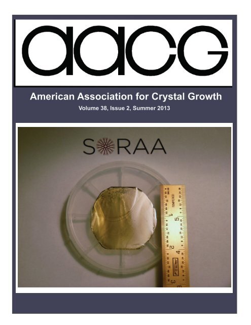
AACG newsletterEDITORCandace LynchInrad Opticsclynch@inradoptics.com201-767-1910 x 583ADVERTISING EDITORDavid Blissdfbliss@gmail.comDESIGN & LAYOUTShoshana Nashaacg@comcast.net303-539-6907Volume 38, Issue 2, Summer 20137 Obituary of Ichiro Sunagawa8 William Bonner Scholarship9 Upcoming Events10 Who will train the next generation ofcrystal growers? By Frank Bruni12 Interview with David Witter by DavidBliss16 Corporate profile: SORAAAACG OFFICERSPRESIDENTPeter SchunemannBAE SystemsVICE PRESIDENTRobert BiefeldSandia National LaboratoryTREASURERDave VanderwaterPhilips-Lumileds LightingSECRETARYJoan RedwingPennsylvania State UniversitySECTION PRESIDENTSWESTEdith Bourret-CourchesneLawrence Berkeley LaboratoryMID-ATLANTICGlen KowachThe City University of New YorkCAPITALRonald G. RosemeierBrimroseOn the cover:2-inch bulk SCoRA GaN crystal, produced at Soraa. See theprofile on page 16 <strong>for</strong> additionalin<strong>for</strong>mation.To opt out of receiving the newsletter, please emailaacg@comcast.net, subject: newsletter opt out.NEW ENGLANDDavid BlissAir Force Research LaboratoryAACG EXECUTIVE ADMINISTRATORShoshana Nash6986 S. Wadsworth Court, Littleton, CO 80128303-539-6907 (phone)303-482-2775 (fax)AACG@comcast.netAACG Newsletter Summer 2013 3
AACG Corporate SupportersAIXTRONwww.aixtron.comLayTec Gmbhwww.laytec.deAKZO Nobel High Purity Metalorganicswww.akzonobel.comAmbrell – Amerithermwww.ameritherm.com<strong>American</strong> <strong>Crystal</strong> Technologywww.axt.comCoherent Advanced <strong>Crystal</strong> Groupwww.coherentinc.com<strong>Crystal</strong> Photonicschai@crystalphotonics.comDockweiler Chemicalswww.dockchemicals.comDow Electric Materialswww.dowelectronicmaterials.comElmet Technologieswww.elmettechnologies.comElsevier BVwww.elsevier.comHeraeus Materials Technologywww.pt-labware.comWafer Technology Ltdwww.wafertech.co.ukFairfield <strong>Crystal</strong>www.fairfieldcrystal.comGT Advanced Technologieswww.gtat.comJohnson Mattheywww.noble.matthey.comK-Space Associateswww.kspace.comMTI Corp.www.mtixtl.comNorthrop Grummanwww.northropgrumman.comNuance Systemswww.nsi-mfg.comThe Olsen FoundationPhotonic Sciencewww.photonic-science.comProChemwww.prochemonline.comSAFC Hitechwww.safcglobal.comSTR Group, Inc.www.semitech.us/Schunk Graphite Technology, LLCwww.schunkgraphite.comThermal Technology Inc.www.thermaltechnologyinc.comThermcraft, Inc.www.thermcraftinc.comVeeco Instruments Inc.www.veeco.comW.C. Hereaus - Engineered Materials Divisionwww.heraeus.comWafertech LLCwww.wafertech.comZircar Ceramics, Inc.www.zircarceramics.comZircar Zirconia, Inc.www.zircarzirconia.com4AACG Newsletter Summer 2013
AACG Newsletter Summer 2013 5
Digital newsletters available on our website atwww.crystalgrowth.org6AACG Newsletter Summer 2013
ObituaryIchiro SunagawaIchiro Sunagawa died of pneumonia on December20th, 2012 at the age of 88. The mourning ceremonywas held in Tokyo on the 24th of December and the funeralwas on the 25th of December. The chief mournerwas his eldest son Jun.Professor Ichiro Sunagawa spent his career activelyinterested in understanding how crystals grow, and whythey exhibit elaborately varied morphology, perfection,and homogeneity. He graduated from Tohoku Universityin 1947 and received a DSc degree from HokkaidoUniversity in 1957 <strong>for</strong> his thesis ‘Morphological variationsin pyrite’.He served <strong>for</strong> 23 years as a mineralogist in the GeologicalSurvey of Japan and <strong>for</strong> 17 years as a Professorof Mineralogy at Tohoku University. From 1989 to2007 he served as Principal of the Yamanashi Instituteof Gemology and Jewelry Arts. In 1991 he was headof the organizing committee of the 9th InternationalConference on <strong>Crystal</strong> <strong>Growth</strong> <strong>for</strong> its meeting in Japan.His initial research work was on understanding theorigins of habit variations in natural minerals, such aspyrite, chalcopyrite, and calcite. This motivated him toinvestigate the surface microtopographs of the crystalfaces of minerals like hematite, diamond, and clays<strong>for</strong>med under a variety of geological conditions. Thisled to a deeper understanding of the morphologies ofcomplex systems based on crystal growth mechanismsat the atomic level.Ichiro SunagawaThis approach opened new windows in Earth andPlanetary Sciences and also in gemology, where heprovided the basic concepts <strong>for</strong> identifying naturalfrom synthetic gemstones. He published many scientificpapers and books on crystal growth, mineralogy,gemology, and diamonds.-with contributions from Dirk and Yumiko Ehrentrautand 50 years Progress in <strong>Crystal</strong> <strong>Growth</strong>AACG Newsletter Summer 2013 7
The William Bonner ScholarshipEach year the AACG offers $10,000 in scholarship moneyto a US member or members of the AACG who areworking in the field of crystal growth. This program wasestablished in 2003 to assist qualified men and womenworking in the field of crystal growth to continue theireducation towards a technical degree. The money <strong>for</strong>these scholarships comes from the Olsen Foundation, ofPrinceton, NJ. A scholarship board of the AACG overseesthe selection of applicants.This year the scholarship award winners are Ryan Franceand Sam Taylor.Ryan France received his MS degree from Boston Universityin 2006. He has worked <strong>for</strong> 5 years as a scientistat NREL, where he is per<strong>for</strong>ming heteroepitaxy of III-Vmaterials by MOVPE and MBE.Ryan France at NREL where he per<strong>for</strong>ms heteroepitaxyof III-V Materials by MOVPE and MBE.While working at NREL, Ryan will be continuing his educationin crystal growth fundamentals. He has completedhis first semester towards a PhD in Materials Science atColorado School of Mines.Sam Taylor graduated from Lehigh University with a BSin Materials Science in 2009. He has worked <strong>for</strong> 2 ½ yearsas an R&D Engineer at TRS Technologies where he doescrystal quality testing, failure analysis, and crystal growthof relaxor-based ferroelectric materials. He is in his firstsemester of graduate studies at Penn State, working towardsa master’s degree. The scholarship will allow Samto continue as a part-time student while working at TRSTechnologies.Sam Taylor is a R&D Engineer at TRSTechnologies while he works towards hismaster’s degree at Penn State.For an application <strong>for</strong>m, contact Shoshana Nashat aaacg@comcast.net. For more in<strong>for</strong>mationvisit www.crystalgrowth.org8AACG Newsletter Summer 2013
Upcoming EventsJuly 7-12, 2013Gordon Conference on Thin Film and <strong>Crystal</strong> <strong>Growth</strong>MechanismsBidde<strong>for</strong>d, MEhttp://www.grc.org/programs.aspx?year=2013&program=thinfilmJuly 21-26, 201319th <strong>American</strong> Conference on <strong>Crystal</strong> <strong>Growth</strong> andEpitaxyKeystone, COhttp://www.crystalgrowth.org/ConferenceLanding.htmlJuly 21-26, 2013International Conference on Defects in SemiconductorsBologna, Italyhttp://www.icds2013.eu/August 11-16, 2013International Conference on <strong>Crystal</strong> <strong>Growth</strong> andEpitaxyWarsaw, PolandAugust 25-30, 2013International Conference on Nitride SemiconductorsWashington, DChttp://www.mrs.org/icns-10/August 25-29, 2013SPIE Optics and Photonics 2013San Diego, CAhttp://www.spie.org/op2/September 29-October 2, 2013International Conference on Silicon Carbide and RelatedMaterials 2013Miyazaki, Japanhttp://icscrm2013.org/Please submit conference in<strong>for</strong>mation to the editor <strong>for</strong>inclusion in future issues.This humorous depiction of enantiomorphs was drawn by Bob Laudise to describe the differencebetween left and right-handed quartz. Thank you to Vince Fratello <strong>for</strong> sharing this cartoon.AACG Newsletter Summer 2013 9
Who will train the next generationof crystal growers?<strong>Crystal</strong> Technology - the synthetic crystal and epilayerproduction including crystal machining and required designand construction of equipment - <strong>for</strong>ms the foundationof the modern electronics revolution and underpinsall aspects of global commerce, communication, energyproduction and medical technology. It is fundamentalto the advances in electricity production, transport andstorage that will be critical to improving energy technologiesto reduce the impact of energy on global climatechange.Contributed by Frank BruniAt the invitation of Dr. Hans Scheel (www.hans-scheel.ch), a group of experienced technologists in this fieldfrom Europe, Asia and the United States convened <strong>for</strong> aweek-long meeting in Poulithra, Arcadia, Greece in May2012.The purpose of this meeting was to discuss the need <strong>for</strong>education and training of the future engineers and scientistswho will <strong>for</strong>m the first generation of specificallytrainedcrystal technologists. Having the basic knowledgeof crystal materials technology (CMT) will enableCMT engineers to consult and collaborate with leadingspecialists of related scientific fields.The goal of the meeting was to generate a white paperoutlining the need <strong>for</strong> this training regimen as well asto include recommended training courses at both undergraduateand graduate levels. This white paper will becirculated to leaders of industry, government and academiawith the goal of promoting this specialized trainingin universities and engineering schools.Among those present, in addition to Dr. Scheel, wereDr. Alexey Borodin, EZAN Chernogolovka, RussianAcademy of Sciences, Prof. Thierry Duffar, Professeurà l’Université de Grenoble, France, Dr. Frank Bruni,Consultant, Cali<strong>for</strong>nia, USA, Prof. Klaus Jacobs, GaNProject Berlin, Germany, Prof. Koichi Kakimoto, Instituteof Applied Mechanics, Kyushu University, Japan,Prof. Georg Roth, Institut für Kristallographie, RWTHAachen, Germany, Prof. Yasuhisa Sano, Dept. of PrecisionEngineering, Osaka University, Japan, Prof. Brian10Mrs. Regula Scheel, Dr. Hans Scheel and Prof. BrianTanner (in background).Tanner, Durham University and Kromek Company, UK,Prof. David Witter, Anaxtal Inc., South Carolina, USAand Prof. Kazuto Yamauchi, Dept. of Precision Engineering,Osaka University, Japan.The meeting was held at the Smyros Resort, located nearthe winter home of Dr. Scheel and Regula Hauser Scheelon the Aegean shore. Hans and Regula organized toursof historical archeological sites that were conducted inbetween technical sessions, presentations and discussions.Locations visited included Olympia, Epidauros, Mycenaeand Athens. A companion program ran in parallelwith the technical sessions and enabled the wives in attendanceto see additional sites of interest.All costs of the conference including meals, housing andexcursions (other than travel to Greece) were subsidizedby Dr. Scheel using retained revenues from prior workshopson crystal growth and technology. In this way theproceeds of the previous workshops could be dedicatedspecifically to the advancement of crystal technologisteducation.AACG Newsletter Summer 2013
At lunch on the harbor at Poulithra.Dr. Bruni (with his wife) returned to Greece in March of2013 to work with Dr. Scheel on completing the whitepaper. The finished document can be found at: https://files.secureserver.net/0fieEZc7s9vyn (use sapphire <strong>for</strong>the password) or through links on the site www.frankbruni.com.Dr. Hans Scheel serves drinks at his home onthe final night of the meeting.AACG Newsletter Summer 2013 11
Interview with David WitterContributed by David BlissDuring his career as a crystal grower and inventor, DavidWitter contributed to many research and development projectsin semiconductor, optical, and magnetic materials. Overthe years, he became an expert at designing control systems<strong>for</strong> crystal growing equipment. He met with David Blissrecently to talk about his experiences.DB: How did you get started in crystal growth?DW: When I started my freshman year at NC State UniversityI got a job as a technician in the Engineering ResearchDepartment growing crystals of sapphire and magnesiumaluminate spinel using a plasma torchfollowing the work of Tom Reed of MIT.After seven years in Ceramic Engineeringat NC State, I took my first job atthe new Union Carbide <strong>Crystal</strong> Products(UCC) plant in San Diego, CA in 1968working <strong>for</strong> G. A. Keig and Fedia Charvat.My education has always benefitedfrom a kind of in<strong>for</strong>mal apprenticeshipsystem.DB: Who did you work with in the earlydays?Morton Jones and Roland Johnson on GGG <strong>for</strong> lasers andmagnetic bubble memories. I was sharing an office withFrank Bruni <strong>for</strong> six months be<strong>for</strong>e he left TI <strong>for</strong> the newAllied Chemical plant in Charlotte.DB: How did you get to know Gordon Teal and Jack Kilby?DW: Gordon Teal came to TI from Bell Labs to be thefirst VP of Research in 1952. He had invented the Teal-Little crystal growth process that later became known asCzochralski growth. Mort Jones had been one of his firstcrystal growers at TI.In 1990, several of the crystal growthprofessionals at TI started the TexasSection of the AACG. I was installedas president. The first meeting washeld at Taffy’s Restaurant. I was ableto get Jack Kilby to come and speak tous when I told him that Gordon Tealwas coming to the meeting. It wasa great evening and Gordon broughtreprints of his first germanium andsilicon crystal growth publications.DW: In San Diego at UCC I met RalphHutcheson; he grew the first ruby lasercrystal <strong>for</strong> Ted Maiman’s laser. Ralphstarted Scientific Materials later in Bozeman,MT. Ted worked <strong>for</strong> the UCC sistercompany “KORAD” in Santa Monica,CA. We had several meeting withthem concerning our YAG and ruby laser components overlunch at the Ball restaurant in Santa Monica.After four years at UCC, I left San Diego and went to workat the Allied Chemical Corporation in Morristown, NJwhere Jack Gillman (dislocations in LiF) was the director. Iworked <strong>for</strong> Bob Linares and M. Alton Gilleo, both <strong>for</strong>merlyof Bell Labs. Then, four years later, Allied moved the groupto Charlotte, NC so I interviewed and found better opportunitieswere available at Lawrence Livermore National Laboratory,Texas Instruments (TI), Motorola and Airtron.I moved to TI Central Research in Dallas in 1976 to work <strong>for</strong>12David WitterJack arrived at the meeting after gettingoff of a plane from Japan just intime to say how significant Gordon’swork was to the invention of the integratedcircuit. Gordon passed awayin 2001 and Jack in 2003.As an Industry Professor at Texas A&M University, I wasasked to represent TI at a faculty senate meeting to recommendJack Kilby <strong>for</strong> an Honorary Doctorate. I rememberstepping outside the building with Jack during the deliberationso that he could smoke several cigarettes. He addedthe TAMU Doctorate to the many honorary doctorates thathe already had from other Universities.Later I worked <strong>for</strong> Jules Levine on the Kilby invention ofa solar array based on single crystal silicon spheres. Mypatented process <strong>for</strong> crystal growth of the spheres went intoproduction many years later at ATS Spheral Solar, but thereAACG Newsletter Summer 2013
were continuing bonding problems between silicon and aluminumand the company withdrew its IPO.DB: How did you manage the transition from GGG to silicon?DW: TI had a policy of promoting transfers with a JobOpportunities Bulletin that came out every Monday. It wasnot necessary to leave TI in order to gain experience withother projects. After the market <strong>for</strong> bubble memory burst in1980 (due to the success of CMOS and the Winchester harddisk technology), I worked on VLSI silicon and grew thefirst 125 mm silicon crystals at TI in the research building. Ifound the IDEA program at TI very useful <strong>for</strong> starting newprojects and in 1983 I became a Senior Member of TechnicalStaff because of my successful IDEA project. Thatproject resulted in the deployment of my automatic crystalgrowth control system using video from the recently inventedcharge-coupled device (CCD) cameras that were muchmore linear and sensitive than vidicon tubes.DB: Did you also work on compound semiconductors?DW: In 1988 two people, a Senior Member of TechnicalStaff and a TI Fellow, left a big hole in the TI crystal growthef<strong>for</strong>t of mercury cadmium telluride (MCT) by resigning inthe same month. I was requisitioned to manage the DefenseAdvanced Research Project Agency (DARPA) project <strong>for</strong>the Traveling Heater Method (THM) growth of MCT <strong>for</strong>cooled focal plane arrays (Javelin Missile). Later it was decidedthat the 90 day long THM process was too expensiveand too difficult <strong>for</strong> development of a reproducible product,and all 25 stations were shut down. A decision was madeto use Liquid Phase Epitaxy (LPE) (a four hour process).After that, I worked on the horizontal Bridgman growth ofcadmium zinc telluride <strong>for</strong> substrates <strong>for</strong> LPE of MCT.DB: Did you work on other projects at TI?DW: In 1991, I transferred to the Uncooled Focal PlaneArray group to make four inch diameter fine-grained bariumstrontium titanate (BST) wafers. BST was a photocapacitor<strong>for</strong> 8-12 micron infrared imaging. We set the phase transitiontemperature to 25 °C and put the device on a thermoelectriccooler to hold it at 25 degrees regardless of the ambient.The dielectric constant of each ceramic pixel changedfrom 500 to 25000 with a two degree change in temperature.A scene viewed through long wavelength infrared optics wasmechanically chopped to produce a video signal. The camerahad fantastic imaging capability due to the uni<strong>for</strong>mityand fine-grained structure in the ceramic wafers. However,laser reticulation of the pixels was slow and not easily replacedby ion milling, so the development ef<strong>for</strong>t shifted toPLZT (lanthanum stabilized lead zirconium titanate) whichnever made it into production of focal plane arrays.DB: Did you work on developing crystal growth equipmentor processing equipment?DW: In 1976 when I first joined TI Jerry Al<strong>for</strong>d, <strong>for</strong>merlyof UCC and Allied, called me to see if I could help himfind an application <strong>for</strong> his Ford Aerospace laser inspectiontechnology developed <strong>for</strong> textiles. I put him in touch withJoe Ayres in Sherman, TX and the whole wafer inspectiontechnology was born.My last years at TI be<strong>for</strong>e retiring in 1998 were in the siliconmaterials department which merged with MEMC in1994, leading to the construction of a $450M 200mm siliconcrystal growth factory. I was the materials manager <strong>for</strong>the critical supplies used in silicon crystal growth. Polysilicon,quartz crucibles, graphite heaters, graphite fiber insulationand boron quality were my responsibility. Everypolished wafer was scanned <strong>for</strong> defects on the commerciallaser inspection stations that had resulted from my earlierresponse to Jerry Al<strong>for</strong>d. Correlation of the scanned defectswith critical material lots and parts used in the growthfurnaces identified problems and kept the yields high.DB: After retirement, did you continue working?DW: Yes, I became Director of Engineering at NorthropGrumman SYNOPTICS in 2000 after I retired from TI andI also started consulting as ANAXTAL. At SYNOPTICS,I emphasized process automation. Weight control systems<strong>for</strong> Czochralski growth were substantially improved usinga rotary contactor with a transduced digital signal instead ofthe low voltage analog signal of the load cell. Since SYN-OPTICS is the merged Litton Airtron and Allied Chemicalfacility that I did not move to in 1976, I felt as though I wasreturning from a 24 year sabbatical at TI.DB: How do you think the US crystal growth communitycan sustain itself, given the migration of crystal growthtechnology to lower-cost countries?DW: The US has outsourced and off-shored much of ourmaterials manufacturing in the last 20 years. There<strong>for</strong>e,our crystal growth technology has suffered tremendously.Only a few companies survive as “National Treasures” andeven some of them have gone offshore <strong>for</strong> their crystallineproduct manufacturing. We need to think smarter and useAACG Newsletter Summer 2013 13
our knowledge more effectively. The National ResearchCouncil has made some recommendations in Report #12640of September 2009 entitled Frontiers of <strong>Crystal</strong>line Matter:From Discovery to <strong>Growth</strong>. Four of the five recommendationsrelate to the education of the next generation of crystalgrowth engineers and scientists. This education should bedone be<strong>for</strong>e the rest of us experienced crystal growers aregone. Some details of my attempt to follow the advice of theNRC are presented in my blog “crystallinematerialsnetwork.blogspot.com”. The link to the NRC Report is also availablethere.DB: Can you give an example of how we can leverage ourknowledge to do smarter production?DW: Consider the silicon solar industry that is now on itsback and going bankrupt as Asian companies are coming into buy up the failed company resources. We need to use asmarter and more energy efficient approach to silicon crystalgrowth. The solar industry has followed the semiconductorindustry into the trap of a very energy intensive “polysilicon”synthesis and remelting process. The resulting oxygenprecipitation defects are beneficial <strong>for</strong> electronic grade wafers,gettering impurities during device processing. However,in solar wafers oxygen precipitates act as recombinationcenters, killing the lifetime. The oxygen comes fromthe dissolution of the quartz crucible during remelting andcrystal growth. We need a new paradigm that avoids remelting– a “disruptive technology” that will save about fiftypercent of the energy used in the present manufacturing process.In 1987, I collaborated with Mohendra Bawa on USpatent 4,710,260 “Deposition of silicon above its meltingpoint”. This patent was never reduced to practice becausethe containment method was unfeasible. I have recently inventeda new containment material and method based on anitrogen economy instead of oxygen. My provisional patentin March of 2009 was followed by a non-provisional patentapplication in March of 2010 which should issue in 2013.With appropriate investors and partners, ANAXTAL silicontechnology will enable direct melt transfer from a silanefeedstock source to the silicon crystal growth process andsave the energy now lost due to the lack of vertical integration.14AACG Newsletter Summer 2013
Announcing theACCGE-19Photo ContestSponsored byJournal of <strong>Crystal</strong> <strong>Growth</strong>Photographs portraying scientific, technical, or artisticaspects of crystals, crystal growth, or characterizationare solicited. The photos will be displayedeach day as a slide show in addition to beingdisplayed in a prominent location at the meeting.Submissions will be voted on by conference attendees,who will be asked to judge entries placedin the following 3 categories:1) Natural untouched micrographs or photographs2) Photographs including digital manipulation (andcomputational simulations)3) Student microscopist/photographerJudging and AwardsAt the ballot box, the images and associated textwill be displayed <strong>for</strong> viewing and judging purposes.Winners will be announced during the Banquet andAwards Ceremony.First-place entries will receive an award and a prizeof $150. If a student wins best entry in the othercategories, they are only eligible <strong>for</strong> one prize. Winningphotos will be published in the AACG newsletter.Contest Rules1) The contest is open to all registered meeting attendees.2) Contestants are allowed to submit one entry percategory.3) Entries must be submitted by email as a highresolution JPEG with a maximum size of 10MB.4) Please do not put text on the photo unless it ispart of the image.5) In a separate text or Word file, please includethe title, name(s), and affiliation(s) along with adescription of the technical significance of the entry,and/or the artistry that it represents (50 wordsor less). Identify the appropriate category <strong>for</strong> judging(untouched micrograph or digitally modified).Student entries should be clearly noted.Entries should be submitted by email to the photocontest organizer, Candace Lynch, by July 5,2013. Please direct any questions or comments tothe organizer:Candace Lynch, Inrad OpticsPhone: 201-767-1910Email: candace.lynch@gmail.comAACG Newsletter Summer 2013 15
Corporate profileSORAAcontributed by Mark D’EvelynSoraa is a vertically-integrated solid state lighting company,with manufacturing capabilities at the wafer, device,and lamp level and development activities in bulkGaN crystals.Soraa was founded in 2008 by Professors Shuji Nakamura,Steve DenBaars, and Jim Speck, world-leadingpioneers in nitride based materials and devices, tocommercialize GaN-on-GaN TM light emitting diodes(LEDs). In 2012, Soraa introduced the world’s firstLED MR16 retrofit lamps with light quality superior tohalogen and efficiency superior to compact fluorescent.Soraa’s full spectrum GaN on GaN LED lamps havesuperior color rendering and beam characteristics comparedto lamps using LEDs created from non-nativesubstrates.SCoRA reactor schematicSoraa is headquartered in Fremont, Cali<strong>for</strong>nia, where itmanufactures its GaN on GaN LEDs in the company’sstate-of-the-art facility.At the LightFair International conference in late April2013, Soraa introduced several second-generation LEDMR16 products, including 65W and 75W halogenequivalentlamps.Soraa’s LEDs are fabricated on bulk GaN substratessynthesized by hydride vapor phase epitaxy (HVPE)and purchased from leading manufacturers. These substratesare significantly more expensive than the sapphirewafers used by most other LED manufacturersand there is obviously a strong desire to reduce costs.Soraa LED MR16 lampsBeginning in 2008, Soraa initiated an in-house researchand development ef<strong>for</strong>t to develop low cost,high quality bulk GaN substrates, with support froma number of U.S. government agencies. Soraa’snovel approach, called SCoRA (Scalable CompactRapid Ammonothermal), differs from conventionalammonothermal methods in that the high pressureapparatus is internally rather than externally heated,is cheaper and more scalable than superalloy autoclaves,and enables growth rates of up to 1 mm perday.Soraa’s bulk crystal growth team includes: Dr. MarkD’Evelyn, who joined Soraa in 2008 following 15years at GE Global Research, where he and his colleaguesworked on CVD and high pressure crystalgrowth of diamond, GaN growth by a not-so-scalablehigh pressure ammonothermal method, growthof radiation-detector crystals and solar-grade silicon,and various other electronic materials and ceramics;Dr. Dirk Ehrentraut, who has broad experiencein bulk crystal growth of GaN, ZnO, doped spinel,ABO 4, A 3B 5O 12, GaPO 4, and various thin-film materials,served as an Associate Professor at TohokuUniversity, and joined Soraa in 2011; and Dr. HakDo Yoo, who has broad manufacturing and researchexperience with silicon and gallium arsenide, servedas President of Silicon Technologies <strong>for</strong> SunPowerCorp., and joined Soraa in 2012.16AACG Newsletter Summer 2013
Recent Government Contracts AwardedNSF SBIR Phase I 2013“Low Cost Scalable Manufacturing of Patterned SapphireSubstrates (PSS) <strong>for</strong> High Efficiency LEDs”Sinmat, Inc. - Gainesville, FLNSF SBIR Phase I 2013“Coilable Single <strong>Crystal</strong> Fibers of Doped YAG <strong>for</strong> HighPower Laser Applications”Shasta <strong>Crystal</strong>s Inc. - Anderson, CANSF SBIR Phase II 2013“Epitaxially Grown GaSb Thin Films on GaAs SubstratesFor Near-Field Conversion of Heat to Electricity”MTPV LLC - Boston, MADOE SBIR Phase I 2013“Monitoring and Control of Chemical Composition of In-GaN Layers During MOCVD”Accustrata, Inc. - College Park, MDDOE STTR Phase I 2013“1200V/ 50A AlGaN-GaN-Si MOS-FETs and SchottkyRectifier”Alameda Applied Sciences Corporation - San Leandro, CADOE SBIR Phase I 2013“FLAAT <strong>Growth</strong> Technology <strong>for</strong> Low Cost Thick HighQuality GaN on 8” sapphire”Kyma Technologies - Raleigh, NCDOE SBIR Phase I 2013“Low Cost High Reproducibility Method <strong>for</strong> GaN SeedProduction”Kyma Technologies - Raleigh, NCDOE SBIR Phase I 2013“High Temperature (300°C) Silicon Carbide (SiC)-BasedVisit our website atIntegrated Gate Drivers <strong>for</strong> Wide Bandgap Power Devices”Arkansas Power Electronics International, Inc. - Fayetteville,ARDOE SBIR Phase II 2013“Thin Diamond Time-of-Flight Detectors”Applied Diamond Inc. - Wilmington, MaDOD Navy SBIR Phase I 2012“High Power Vertical Gallium Nitride (GaN) Transistors onNative GaN Substrates <strong>for</strong> Power Switching Applications”Avogy Inc. - San Jose, CADOD Navy STTR Phase I 2012“High-Power Semiconductor Laser in the 3.0- to 3.5-μmSpectral Range”sdPhotonics LLC - Oviedo, FLDOD Navy SBIR Phase I 2012“Cost-Effective Technologies <strong>for</strong> Fabrication of Piezo <strong>Crystal</strong>Vector Velocity Sensors”TRS Ceramics Inc. - State College, PADOD Army STTR Phase I 2012“HOVPE <strong>Growth</strong> of High Quality AlGaN on AlN Substrates”Structured Materials Industries - Piscataway, NJDOD Army STTR Phase I 2012“High-Quality AlGaN Epitaxial Films on GaN and AlNSubstrates”Adroit Materials - Raleigh, NCDOD Army STTR Phase I 2012“High Quality, Low Cost, and High Purity AlGaN Epitaxywith Reduced Surface Dislocation Density”Kyma Technologies, Inc. - Raleigh, NCADVERTISE IN THENEWSLETTER!The AACG newsletter is themost effective medium <strong>for</strong>reaching the <strong>American</strong> crystalgrowth community.Contact the AACG Administrator atwww.crystalgrowth.orgAACG Newsletter Summer 2013 aacg@comcast.net <strong>for</strong> more in<strong>for</strong>mation.17
Career OpportunitiesCoherent – East Hanover, NJCACG is seeking candidates to fill a position in ourmanufacturing growth department. Responsibilities willinclude but not limited to assisting production crystalgrowth.Previous experience in high temperature bulk crystalgrowth techniques is desired. An educational backgroundin ceramics, chemistry, or physics is desired.The candidate must be able to function within a teamenvironment; communicate, collaborate and interact withmanufacturing operations and R&D alike. Training willbe provided. Any technical degree from Associates toBA or BS in a relevant discipline. Must be able to workflexible hours.Please apply on the www. Coherent.com website,job#3608Cree – Durham, NCWe currently have the need <strong>for</strong> a Senior ProcessDevelopment Engineer to support our Materials grouplocated at our headquarter facility in Durham, NC.Materials Business is looking <strong>for</strong> a high potential,resourceful, hands-on, problem solving developmentengineer with a good understanding of the materialsbehavior and capacity to quickly grasp and resolvetechnical challenges . A well-built background insemiconductor manufacturing with strong leadershipskills is necessary to enable successful execution ofboth new process development and improvementof existing processes in a fast paced manufacturingenvironment.The successful candidate will maintain a regularinterface with Cree’s suppliers on quality issues andresolution, working with procurement and qualitycontrol teams.http://autohire.careershop.com/creeEquipment Available- (2) Czochralski <strong>Crystal</strong> Growers- Very lightly used (8-10 runs each)- Configured <strong>for</strong> silicon growth- Automated control system- 150 kg lift capacity- Furnace ID: 1000 mm- Pull chamber ID: 310 mm- Pull chamber height: 2500 mm- Includes (2) 22” graphite hot zones- Complete systemsContact: Bob StevensonGT Advanced Technologies603-681-3816bob.stevenson@gtat.com18AACG Newsletter Summer 2013
<strong>Crystal</strong> IS- Albany, New York<strong>Crystal</strong> IS is looking to hire a Senior <strong>Crystal</strong> <strong>Growth</strong>Engineer at its’ Albany, NY Corporate Headquarters.This is a new role that will have a tremendous opportunityto impact the growth and success of <strong>Crystal</strong> IS.We are looking <strong>for</strong> an experienced professional to leadthe process development, process improvement, and integrationof our core AlN bulk growth technology andassume responsible <strong>for</strong> process (and quality) transferfrom R&D to production.We are looking to identify and hire an inventive handsonleader focused on achieving results. The qualifiedcandidate will be a self-motivated team player who canlead technology and people.From a technology perspective we require demonstrated experiencegenerating new ideas that result in IP and leadingproblem solving and new technology implementation initiatives.From a people leadership perspective you should beable to demonstrate past successes leading, mentoring anddeveloping staff.http://www.cisuvc.com/about/careersCurrent job openings are listed on the AACG website,along with additional details regarding the jobs postedabove. If you would like to advertise an open position inthe newsletter or on the website, please contact aacg@comcast.net.AACG Newsletter Summer 2013 19