Reduction of Leakage current Generated by Degradation in Organic ...
Reduction of Leakage current Generated by Degradation in Organic ...
Reduction of Leakage current Generated by Degradation in Organic ...

Create successful ePaper yourself
Turn your PDF publications into a flip-book with our unique Google optimized e-Paper software.
P1-12 / H. D. Hwang<br />
<strong>Reduction</strong> <strong>of</strong> <strong>Leakage</strong> <strong>current</strong> <strong>Generated</strong> <strong>by</strong> <strong>Degradation</strong> <strong>in</strong><br />
<strong>Organic</strong> Th<strong>in</strong> Film Transistors us<strong>in</strong>g Pattern on Pentacene<br />
Surface <strong>by</strong> Atomic Force Microscope<br />
Hyun Doo Hwang 1 , Hyunsuck Kim 1 , Chang Ho Kim 2 and Jae-Hoon Kim 1,2 *<br />
1 Dept. <strong>of</strong> Electronics and Computer Eng<strong>in</strong>eer<strong>in</strong>g, Hanyang University, Seoul, Korea<br />
2 Research Institute <strong>of</strong> Information Display, Hanyang University, Seoul, Korea<br />
Phone: +82-2-2220-0343 , E-mail: jhoon@hanyang.ac.kr<br />
Abstract<br />
In this paper, we proposed a simple method <strong>of</strong> decreas<strong>in</strong>g<br />
the <strong>of</strong>f <strong>current</strong> generated <strong>by</strong> degradation for improve the<br />
electrical characteristics such as mobility and on/<strong>of</strong>f<br />
<strong>current</strong> ratio <strong>by</strong> mak<strong>in</strong>g the l<strong>in</strong>e patterns on the pentacene<br />
surface between the electrodes us<strong>in</strong>g atomic force<br />
microscope (AFM) lithography.<br />
1. Introduction<br />
Intensive <strong>in</strong>terest <strong>in</strong> organic th<strong>in</strong> film transistors<br />
(OTFTs) ow<strong>in</strong>g to their simple and low-temperature<br />
process has expedited efforts to develop commercial<br />
applications for OTFTs <strong>in</strong> electronic devices, such as<br />
driv<strong>in</strong>g elements for flexible displays, RFID tags, and<br />
large-area sensor [1-3]. However, <strong>in</strong> spite <strong>of</strong><br />
remarkable progress <strong>in</strong> device performances, OTFTs<br />
still suffer from the characteristic degradation <strong>by</strong><br />
moisture and oxygen <strong>in</strong> air [4]. The H2O molecules <strong>in</strong><br />
air makes the traps <strong>in</strong> pentacene layer that will be<br />
captur<strong>in</strong>g charges <strong>in</strong> on state, lead<strong>in</strong>g to an <strong>in</strong>crease <strong>in</strong><br />
the conductivity between source and dra<strong>in</strong> when the<br />
device is <strong>in</strong> <strong>of</strong>f state and result<strong>in</strong>g <strong>in</strong> a decrease <strong>of</strong> the<br />
on/<strong>of</strong>f <strong>current</strong> ratio [5]. <strong>Degradation</strong> <strong>by</strong> H2O<br />
molecules starts on the top surface <strong>of</strong> pentacene layer<br />
and slowly extends to the bottom <strong>of</strong> pentacene film<br />
[6].<br />
In this paper, we made a l<strong>in</strong>e pattern to reduce the<br />
<strong>in</strong>creas<strong>in</strong>g <strong>of</strong> leakage <strong>current</strong> <strong>by</strong> degradation for<br />
ma<strong>in</strong>tenance <strong>of</strong> on/<strong>of</strong>f <strong>current</strong> ratio <strong>by</strong> cutt<strong>in</strong>g <strong>of</strong>f the<br />
<strong>current</strong> path <strong>in</strong> pentacene surface us<strong>in</strong>g atomic force<br />
microscopy (AFM). AFM based nan<strong>of</strong>abrication<br />
methods attract much <strong>in</strong>terest for their ultra-high<br />
resolution, easy operation, and low equipment costs.<br />
AFM lithography methods are realized <strong>by</strong> us<strong>in</strong>g<br />
different <strong>in</strong>teraction forces between the tip and the<br />
sample surface, such as physical, chemical and<br />
• IMID 2009 DIGEST<br />
Keywords: AFM, nano pattern, OTFT, pentacene, leakage <strong>current</strong><br />
mechanical forces. Because the curvature radius <strong>of</strong><br />
AFM tip and the distance between the tip and the<br />
sample are both on the nano scale, local fields, such as<br />
force field and electric field, on the nano scale are<br />
generated. These local fields modify the sample<br />
surface and construct various nanostructures. AFM<br />
mechanical lithography makes scratch and <strong>in</strong>dention<br />
on various material surfaces on the nano scale <strong>by</strong><br />
apply<strong>in</strong>g a suitable force, and then nano patterns are<br />
obta<strong>in</strong>ed <strong>by</strong> controll<strong>in</strong>g the movement <strong>of</strong> the tip.<br />
2. Experimental<br />
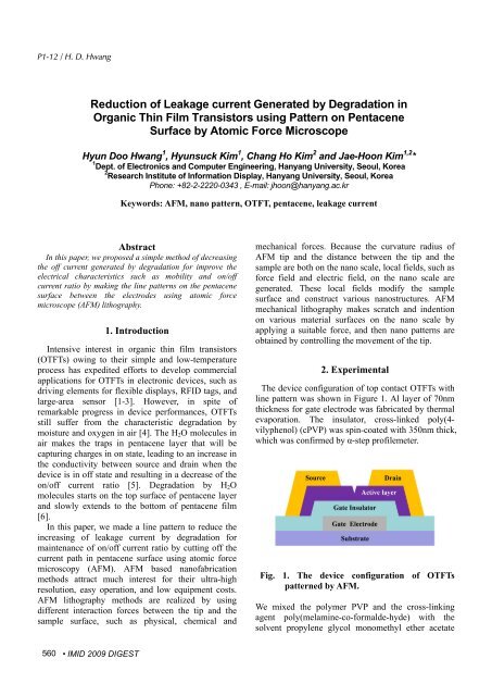
The device configuration <strong>of</strong> top contact OTFTs with<br />
l<strong>in</strong>e pattern was shown <strong>in</strong> Figure 1. Al layer <strong>of</strong> 70nm<br />
thickness for gate electrode was fabricated <strong>by</strong> thermal<br />
evaporation. The <strong>in</strong>sulator, cross-l<strong>in</strong>ked poly(4vilyphenol)<br />
(cPVP) was sp<strong>in</strong>-coated with 350nm thick,<br />
which was confirmed <strong>by</strong> α-step pr<strong>of</strong>ilemeter.<br />
Fig. 1. The device configuration <strong>of</strong> OTFTs<br />
patterned <strong>by</strong> AFM.<br />
We mixed the polymer PVP and the cross-l<strong>in</strong>k<strong>in</strong>g<br />
agent poly(melam<strong>in</strong>e-co-formalde-hyde) with the<br />
solvent propylene glycol monomethyl ether acetate
(PGMEA). The pentacene purified <strong>by</strong> sublimation was<br />
thermally evaporated under pressure <strong>of</strong> 10 -6 Torr. The<br />
thickness <strong>of</strong> the pentacene layer is 60nm, and the<br />
deposition rate was 0.5 Å/sec. The 400nm thick<br />
electrodes <strong>of</strong> gold were prepared. The channel length<br />
and width <strong>in</strong> our OTFTs were 50um and 300um,<br />
respectively. Atomic force microscopy lithography<br />
was performed us<strong>in</strong>g a PSIA XE-100 <strong>in</strong>strument.<br />
Diamond coated AFM probes (DT-NCHR) <strong>in</strong> contact<br />
mode were used dur<strong>in</strong>g drew a l<strong>in</strong>e on the pentacene<br />
film (Fig. 2). This AFM probe was also <strong>in</strong> some cases<br />
used for imag<strong>in</strong>g, but most <strong>of</strong> the AFM imag<strong>in</strong>g was<br />
performed <strong>in</strong> non-contact mode us<strong>in</strong>g NCHR or<br />
NCLR probes.<br />
Fig. 2. AFM images <strong>of</strong> l<strong>in</strong>e pattern on pentacene<br />
surface.<br />
3. Results and discussion<br />
Figure 3 shows the comparison <strong>of</strong> <strong>current</strong><br />
characteristics for the sample us<strong>in</strong>g oxidized<br />
pentacene with and without patterns <strong>in</strong><br />
Insulator/Semiconductor/Metal (ISM) structure (i.e.<br />
the l<strong>in</strong>es us<strong>in</strong>g AFM lithography). The slope <strong>in</strong> the I-V<br />
curve for patterned device is larger than without<br />
P1-12 / H. D. Hwang<br />
pattern’s one. This phenomenon could be expla<strong>in</strong>ed<br />
the pattern <strong>in</strong>terrupt the <strong>current</strong> flow near the<br />
pentacene surface, as a result, the leakage <strong>current</strong> was<br />
decreased.<br />
Normalized Current<br />
10 1<br />
10 0<br />
10 -1<br />
<strong>in</strong>creased<br />
decreased<br />
unpatterned Pn<br />
patterned Pn<br />
0 10 20 30 40<br />
Voltage [V]<br />
Fig. 3. Current versus voltage for leakage <strong>current</strong> <strong>in</strong><br />
ISM structure.<br />
Figure 4 shows the transfer characteristics <strong>of</strong> OTFTs<br />
with and without pattern on pentacene surface. The<br />
chemical reaction between pentacene and H2O<br />
molecules <strong>in</strong>duce free charge <strong>in</strong>creas<strong>in</strong>g the<br />
conductivity between source and dra<strong>in</strong> on the surface<br />
<strong>of</strong> pentacene accord<strong>in</strong>g to the time. The <strong>in</strong>creased<br />
conductivity <strong>by</strong> degradation leads to gradually<br />
<strong>in</strong>crease <strong>of</strong> leakage <strong>current</strong> shown <strong>in</strong> Figure 4(b). In<br />
contrast, a l<strong>in</strong>e pattern formed <strong>by</strong> AFM lithography<br />
with ~25nm depth reduced the leakage <strong>current</strong><br />
<strong>in</strong>creased <strong>by</strong> degradation <strong>by</strong> cutt<strong>in</strong>g <strong>of</strong>f the <strong>current</strong><br />
path <strong>in</strong> pentacene surface. The resistance <strong>of</strong> pentacene<br />
surface <strong>in</strong>creased <strong>by</strong> a pattern, and the surface leakage<br />
<strong>current</strong> <strong>by</strong> degradation was decreased.<br />
The threshold voltage shift to positive direction was<br />
caused <strong>by</strong> the electrical characteristics <strong>of</strong> degradation<br />
<strong>of</strong> cPVP <strong>in</strong>sulator layer (Fig. 4) [7]. The bias stress<br />
was caused <strong>by</strong> water absorbed <strong>in</strong>to the bottom<br />
dielectric layer far away from the conduct<strong>in</strong>g channel.<br />
The effect <strong>of</strong> absorbed water molecules is a slow<br />
change <strong>of</strong> the effective electric field dur<strong>in</strong>g device<br />
operation that leads to the positive shift <strong>in</strong> threshold<br />
voltage.<br />
IMID 2009 DIGEST •
P1-12 / H. D. Hwang<br />
(a)<br />
Dra<strong>in</strong>-Source Current [A]<br />
(b)<br />
Dra<strong>in</strong>-Source Current [A]<br />
1E-3<br />
1E-5<br />
1E-7<br />
1E-9<br />
1E-11<br />
1E-3<br />
1E-5<br />
1E-7<br />
1E-9<br />
1E-11<br />
0<br />
-45 -30 -15 0 15 30<br />
• IMID 2009 DIGEST<br />
1st measurement<br />
2nd measurement after 1 h<br />
3rd measurement after 24 h<br />
Gate-Source Voltage [V]<br />
1st measurement<br />
2nd measurement after 1 h<br />
3rd measurement after 24 h<br />
0<br />
-45 -30 -15 0 15 30<br />
Gate-Source Voltage [V]<br />
Fig. 4. The electrical characteristics <strong>of</strong> OTFTs (a)<br />
with and (b) without pattern on pentacene<br />
surface.<br />
4. Summary<br />
We proposed the simple method to improve the<br />
electrical characteristics <strong>of</strong> OTFT us<strong>in</strong>g the<br />
lithography <strong>by</strong> AFM. We could decreased the surface<br />
leakage <strong>current</strong> <strong>by</strong> mak<strong>in</strong>g the l<strong>in</strong>es hav<strong>in</strong>g enough<br />
depth and length on the pentacene surface between<br />
electrodes which have the perpendicular direction<br />
aga<strong>in</strong>st electric field for improv<strong>in</strong>g the characteristics<br />
such as mobility and on/<strong>of</strong>f ratio. Hereafter, additional<br />
experiments will be performed to analyze the<br />
electrical performance <strong>of</strong> OTFT for vary<strong>in</strong>g the depth,<br />
length, and numbers <strong>of</strong> l<strong>in</strong>es.<br />
8<br />
6<br />
4<br />
(Dra<strong>in</strong>-Source<br />
2<br />
Current)1/2 [mA]<br />
8<br />
6<br />
4<br />
(Dra<strong>in</strong>-Source<br />
2<br />
Current)1/2 [mA]<br />
Acknowledgement<br />
This research was supported <strong>by</strong> a grant(F0004120-<br />
2008-31) from Information Display R&D Center, one<br />
<strong>of</strong> the 21 st Century Frontier R&D Program funded <strong>by</strong><br />
the M<strong>in</strong>istry <strong>of</strong> Knowledge Economy <strong>of</strong> Korean<br />
government.<br />
5. References<br />
1. S. R. Forrest, Nature, 428, p.911-918 (2004).<br />
2. R. Rotzoll, S. Mohapatra, V. Olariu, R. Wenz, M.<br />
Grigas and K. Dimmler, Appl. Phys. Lett., 88,<br />
p.123502 (2006).<br />
3. L. Wang, D. F<strong>in</strong>e, S. I. Khondaker, T. Jung and A.<br />
Dodabalapu, Sens. Actuators, 113, p.539-544<br />
(2000).<br />
4. T. Jung, A. Dodabalapur, R. Wenz and S.<br />
Mohapatra, Appl. Phys. Lett., 87, p.182109<br />
(2005).<br />
5. Y. Qiu, Y. Hu, G. Dong, L. Wang, J. Xie and Y.<br />
Ma, Appl. Phys. Lett., 83, p.1644 (2003).<br />
6. M. L<strong>in</strong>g, Z. Bao and D. Li, Appl. Phys. Lett., 88,<br />
p.033502 (2006).<br />
7. T. N. Ng, J. H. Daniel, S. Sambandan, A. C. Arias,<br />
M. L. Chab<strong>in</strong>yc, and R. A. Street, J. Appl. Phys,<br />
103, p.044506 (2008).