Thermal Imaging with Novel Infrared Focal Plane Arrays - NASA Jet ...
Thermal Imaging with Novel Infrared Focal Plane Arrays - NASA Jet ...
Thermal Imaging with Novel Infrared Focal Plane Arrays - NASA Jet ...

You also want an ePaper? Increase the reach of your titles
YUMPU automatically turns print PDFs into web optimized ePapers that Google loves.
<strong>Thermal</strong> <strong>Imaging</strong> <strong>with</strong> <strong>Novel</strong> <strong>Infrared</strong> <strong>Focal</strong> <strong>Plane</strong> <strong>Arrays</strong> and Quantitative Analysis of<br />
<strong>Thermal</strong> Imagery<br />
S. D. Gunapala, S. B. Rafol, S. V. Bandara, J. K. Liu, J. M. Mumolo, A. Soibel, and D. Z. Ting<br />
Center for <strong>Infrared</strong> Sensors, <strong>Jet</strong> Propulsion Laboratory, California Institute of Technology, Pasadena, CA 91109, U.S.A.<br />
ABSTRACT<br />
We have developed a single long-wavelength infrared (LWIR) quantum well infrared photodetector (QWIP)<br />
camera for thermography. This camera has been used to measure the temperature profile of patients. A pixel coregistered<br />
simultaneously reading mid-wavelength infrared (MWIR)/LWIR dual-band QWIP camera was developed to<br />
improve the accuracy of temperature measurements especially <strong>with</strong> objects <strong>with</strong> unknown emissivity. Even the dualband<br />
measurement can provide inaccurate results due to the fact that emissivity is a function of wavelength. Thus we<br />
have been developing a four-band QWIP camera for accurate temperature measurement of remote object.<br />
Key Words: Quantum-wells, <strong>Focal</strong> planes, Dual-band infrared, Thermography<br />
1. INTRODUCTION<br />
There are many applications that require long<br />
wavelength, large, uniform, reproducible, low cost, low<br />
1/f noise, low power dissipation, and radiation hard<br />
infrared (IR) focal plane arrays (FPAs). However, the<br />
need for smaller, lighter and lower cost imaging<br />
radiometers is now apparent, particularly in missions<br />
that combine different types of remote sensing<br />
instruments. A quantum well designed to detect<br />
infrared (IR) light is called a quantum well infrared<br />
photodetector (QWIP). An elegant candidate for QWIP<br />
is the square quantum well of basic quantum<br />
mechanics [1]. When the quantum well is sufficiently<br />
deep and narrow, its energy states are quantized<br />
(discrete). The potential depth and width of the well can<br />
be adjusted so that it holds only two energy states: a<br />
ground state near the well bottom, and a first excited<br />
state near the well top. A photon striking the well will<br />
excite an electron in the ground state to the first excited<br />
state, then an externally-applied voltage sweeps it out<br />
producing a photocurrent (Fig. 1). Only photons having<br />
energies corresponding to the energy separation<br />
between the two states are absorbed, resulting in a<br />
detector <strong>with</strong> a sharp absorption spectrum. Designing a<br />
quantum well to detect light of a particular wavelength<br />
becomes a simple matter of tailoring the potential depth<br />
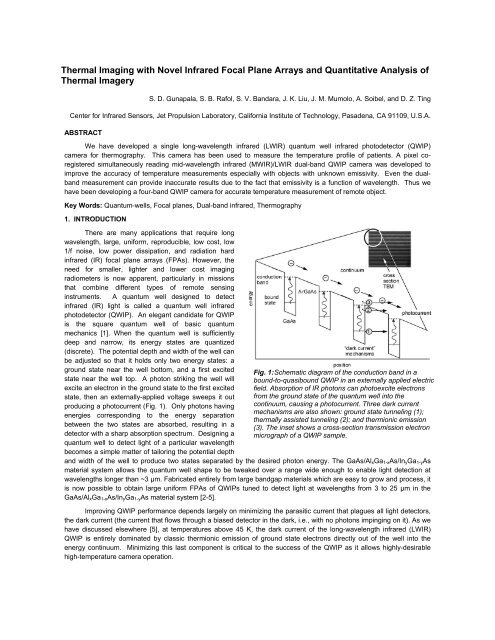
Fig. 1: Schematic diagram of the conduction band in a<br />
bound-to-quasibound QWIP in an externally applied electric<br />
field. Absorption of IR photons can photoexcite electrons<br />
from the ground state of the quantum well into the<br />
continuum, causing a photocurrent. Three dark current<br />
mechanisms are also shown: ground state tunneling (1);<br />
thermally assisted tunneling (2); and thermionic emission<br />
(3). The inset shows a cross-section transmission electron<br />
micrograph of a QWIP sample.<br />
and width of the well to produce two states separated by the desired photon energy. The GaAs/AlxGa1-xAs/InyGa1-yAs<br />
material system allows the quantum well shape to be tweaked over a range wide enough to enable light detection at<br />
wavelengths longer than ~3 µm. Fabricated entirely from large bandgap materials which are easy to grow and process, it<br />
is now possible to obtain large uniform FPAs of QWIPs tuned to detect light at wavelengths from 3 to 25 µm in the<br />
GaAs/AlxGa1-xAs/InyGa1-yAs material system [2-5].<br />
Improving QWIP performance depends largely on minimizing the parasitic current that plagues all light detectors,<br />
the dark current (the current that flows through a biased detector in the dark, i.e., <strong>with</strong> no photons impinging on it). As we<br />
have discussed elsewhere [5], at temperatures above 45 K, the dark current of the long-wavelength infrared (LWIR)<br />
QWIP is entirely dominated by classic thermionic emission of ground state electrons directly out of the well into the<br />
energy continuum. Minimizing this last component is critical to the success of the QWIP as it allows highly-desirable<br />
high-temperature camera operation.
Therefore, we have designed the bound-toquasibound<br />
[1] quantum well by placing the first excited<br />
state exactly at the well top as shown in Fig. 1.<br />
Dropping the first excited state to the well top causes<br />
the barrier to thermionic emission (roughly the energy<br />
height from the ground state to the well top) to be ~10<br />
meV more in our bound-to-quasibound QWIP than in<br />
the bound-to-continuum QWIP, theoretically causing<br />
the dark current to drop by a factor of ~6 at a<br />
temperature of 70 K [2,3]. The dark current as a<br />
function of temperature of the 8.5 µm peaked bound-toquasibound<br />
QWIP is shown in Fig. 2. This compares<br />
well <strong>with</strong> the factor of ~4 drop we experimentally<br />
observe compared to the bound-to-continuum QWIP<br />
having the same peak wavelength.<br />
Fig. 3: Responsivity spectrum of a bound-to-quasibound<br />
LWIR QWIP test structure at temperature T = 77 K. The<br />
spectral response peak is at 8.5 µm and the long wavelength<br />
cutoff is at 8.9 µm.<br />
Fig. 2: Dark current of 8.5 µm peaked bound-to-quasibound<br />
QWIP as a function of temperature. Data were taken <strong>with</strong> a<br />
200 µm diameter test structure and normalized to 25x25 µm 2<br />
pixel.<br />
2. TEST STRUCTURE RESULTS<br />
Each period of the multi-quantum well (MQW)<br />
structure consists of a 45 Å well of GaAs (doped n =<br />
5x10 17 cm -3 ) and a 500 Å barrier of Al0.3Ga0.7As.<br />
Stacking many identical quantum wells (typically 50)<br />
together increases photon absorption. Ground state<br />
electrons are provided in the detector by doping the<br />
GaAs well layers <strong>with</strong> Si. This photosensitive MQW<br />
structure is sandwiched between 0.5 µm GaAs top and<br />
bottom contact layers doped n = 5x10 17 cm -3 , grown on<br />
a semi-insulating GaAs substrate by molecular beam<br />
epitaxy (MBE). Then a 0.7 µm thick GaAs cap layer on<br />
top of a 300 Å Al0.3Ga0.7As stop-etch layer was grown<br />
in situ on top of the device structure to fabricate the<br />
light coupling optical cavity. The epitaxially grown<br />
material was processed into 200 µm diameter mesa<br />
test structures (area = 3.14x10 -4 cm 2 ) using wet<br />
chemical etching, and Au/Ge ohmic contacts were evaporated onto the top and bottom contact layers.<br />
The detectors were back illuminated through a 45° polished facet [5] and a responsivity spectrum is shown in Fig.<br />
3. The responsivity of the detector peaks at 8.5 µm and the peak responsivity (Rp) of the detector is 83 mA/W at bias VB<br />
= -1.1 V. The spectral width and the cutoff wavelength are ��/� = 10% and �c = 8.9 µm respectively. The measured<br />
absolute peak responsivity of the detector is small, up to about VB = -0.5 V. Beyond that it increases nearly linearly <strong>with</strong><br />
bias reaching RP = 420 mA/W at VB = -5 V. This type of behavior of responsivity versus bias is typical for a bound-toquasibound<br />
QWIP. The peak quantum efficiency was 1.4% at bias VB = -1.1 V for a 45° double pass.<br />
The peak detectivity is defined as , where RP is the peak responsivity, A is the area of the<br />
detector and A = 3.14x10 -4 cm 2 . The measured peak detectivity at bias VB = -1.1 V and temperature T = 65 K is 1x10 11<br />
D P � R P AB / i n<br />
cm�Hz/W. Figure 4 shows the bias dependence of peak detectivity as a function of temperature. These detectors show<br />
BLIP at bias VB = -2 V and temperature T = 72 K for a 300 K background <strong>with</strong> f/2 optics.
3. 640x512 FORMAT FOCAL PLANES<br />
Fig. 4: Detectivity as a function of temperatures at bias of<br />
1.1 V.<br />
Fig. 5: NEDT histogram of the 327,680 pixels of the 640x512<br />
array showing a high uniformity of the FPA.<br />
A 640x512 QWIP FPA hybrid was mounted onto a 330<br />
mW integral Sterling closed-cycle cooler assembly and installed<br />
into an Indigo Phoenix� camera-body, to demonstrate a handheld<br />
LWIR camera (shown in Fig. 6). The Phoenix� infrared<br />
camera system has been developed by Indigo Systems<br />
Corporation to meet the needs of the research, industrial and<br />
ruggedized OEM communities. The system is comprised of a<br />
camera head and a selection of two video processing back ends.<br />
The camera head was made of Indigo’s standard 640x512<br />
format readout ISC 9803, mated to long-wavelength QWIP<br />
detector materials. Two video processing units are the Real Time<br />
<strong>Imaging</strong> Electronics (RTIE) that provide conventional NTSC<br />
After the 2-D grating array was defined by<br />
the lithography and reactive ion etching, the<br />
photoconductive QWIPs of the 640x512 FPAs were<br />
fabricated by dry etching through the photosensitive<br />
GaAs/AlxGa1-xAs multi-quantum well layers into the<br />
0.5 µm thick doped GaAs bottom contact layer. The<br />
pitch of the FPA is 25 µm and the actual pixel size<br />
is 23x23 µm 2 . The 2-D gratings on top of the<br />
detectors were then covered <strong>with</strong> Au/Ge and Au for<br />
Ohmic contact and reflection. Figure 6 shows<br />
twelve processed QWIP FPAs on a 3 inch GaAs<br />
wafer. Indium bumps were then evaporated on top<br />
of the detectors for Si readout circuit (ROC)<br />
hybridization. A single QWIP FPA was chosen and<br />
hybridized (via indium bump-bonding process) to a<br />
640x512 CMOS multiplexer (ISC 9803) and biased<br />
at VB = -1.1 V. At temperatures below 72 K, the<br />
signal to noise ratio of the system is limited by array<br />
non-uniformity, multiplexer readout noise, and<br />
photo current (photon flux) noise. At temperatures<br />
above 72 K, temporal noise due to the QWIP’s<br />
higher dark current becomes the limitation. This<br />
initial array gave excellent images <strong>with</strong> 99.92% of<br />
the pixels working (number of dead pixels � 250),<br />
demonstrating the high yield of GaAs technology.<br />
The operability was defined as the percentage of<br />
pixels having noise equivalent differential<br />
temperature less than 100 mK at 300 K background<br />
and in this case operability happens to be equal to<br />
the pixel yield. Figure 5 shows the measured NE�T<br />
of the FPA at an operating temperature of T = 65 K,<br />
16 msec integration time, bias VB = -1.1 V for 300 K<br />
background <strong>with</strong> f/2 optics and the mean value is<br />
20 mK. This agrees reasonably <strong>with</strong> our estimated<br />
value of 10 mK based on test structure data. The<br />
net peak quantum efficiency of the FPA was 1.4%<br />
4. 640x512 PIXEL HAND-HELD CAMERA<br />
AND QUANTITATIVE INFRARED IMAGERY<br />
Fig. 6: Picture of the 640x512 hand-held long wavelength<br />
QWIP camera (QWIP Phoenix).
video as well as corrected parallel digital video out at video rates and the Digital Acquisition System (DAS) that provides<br />
high-speed (40 MHz) raw digital data acquisition and output <strong>with</strong> limited real time video for system setup and focusing.<br />
The other element of the camera is a 100 mm focal length germanium lens, <strong>with</strong> a 5.5 degree field of view. It is designed<br />
to be transparent in the 7-14 µm wavelength range, to be compatible <strong>with</strong> the QWIP’s 8.5 µm operation. The digital<br />
acquisition resolution of the camera is 14-bits, which determines the instantaneous dynamic range of the camera (i.e.,<br />
16,384).<br />
The measured mean NE�T of the QWIP camera is<br />
20 mK (the higher NEDT is due to the 65% transmission<br />
through the lens assembly) at an operating temperature of<br />
T = 65 K and bias VB = -1.1 V, for a 300 K background <strong>with</strong><br />
germanium f/2 optics. The uncorrected photocurrent nonuniformity<br />
(which includes a 1% non-uniformity of the ROIC<br />
and a 1.4% non-uniformity due to the cold-stop in front of<br />
the FPA not yielding the same field of view to all the pixels)<br />
of the 327,680 pixels of the 640x512 FPA is about 5% (=<br />
sigma/mean). The non-uniformity after two-point (17˚ and<br />
27˚ Celsius) correction improves to an impressive 0.02%.<br />
After correction, measurements of the residual nonuniformity<br />
were made at temperatures ranging from 12<br />
Celsius (the cold temperature limit of the blackbody) up to<br />
42 degrees Celsius. The non-uniformity at each<br />
temperature was found by averaging 16 frames, calculating<br />
the standard deviation of the pixel-to-pixel variation of the<br />
16 frames average and then dividing by the mean output,<br />
producing non-uniformity that may be reported as a<br />
Fig. 7. Residual non-uniformity after two-point<br />
correction as a function of scene temperature.<br />
This corrected non-uniformity range is<br />
comparable to 3-5 μm infrared cameras.<br />
percentage. For camera systems that have NE�T of about 20 mK, the corrected image must have less than 0.1% nonuniformity<br />
in order to be TV quality. Figure 7 shows the residual non-uniformity of the camera after two-point correction<br />
as a function of scene temperature. Also it is clearly evident from Fig. 7 that the camera’s performance is outstanding in<br />
this scene temperature range, and its residual non-uniformity did not exceed 0.03% <strong>with</strong>in the entire scene temperature<br />
range of 12 – 42 Celsius.<br />
98 0 F<br />
96 0 F<br />
94 0 F<br />
92 0 F<br />
90 0 F<br />
88 0 F<br />
86 0 F<br />
84 0 F<br />
82 0 F<br />
80 0 F<br />
78 0 F<br />
76 0 F<br />
Video images were taken at a frame rate of 30 Hz at temperatures as high as T = 65 K, using a ROIC capacitor<br />
having a charge capacity of 11x106 electrons (the maximum number of photoelectrons and dark electrons that can be<br />
counted in the time taken to read each detector pixel). Figure 8 shows one frame of a video image taken <strong>with</strong> a 9 µm<br />
cutoff 640x512 pixel QWIP Phoenix camera. The temperature was calculated assuming 0.8 emissivity using the<br />
following equation,<br />
� � R ( )<br />
~<br />
Fig. 8. This figure shows the temperature variation of the toes and elbows of a leprosy patient.<br />
�H<br />
I p � RpG<br />
� d�<br />
�(<br />
� ) M ( �,<br />
T T)<br />
�<br />
�L
where, G, R(�), E(�), �L, �H, M(�,TT), and RP are the optical gain, normalized responsivity verses wavelength function,<br />
emissivity as a function of wavelength, lower and upper limit of the detector wavelength response, spectral exitance of<br />
the source at temperature, and peak responsivity of the detector respectively.<br />
5. DUAL-BAND INFRARED IMAGERY<br />
The spectral response of QWIPs are inherently narrow-band and the typical full-width at half-maximum (FWHM) is<br />
about 10% of the peak wavelength. This makes it suitable for fabrication of negligible optical cross-talk dual-band<br />
detector arrays. This shortfall in single band detector measurement due to unknown emissivity can be overcome by<br />
taking the ratio of the signals measured at two different wavelengths using a dual-band detector. If we assume negligible<br />
variation of emissivity in thermal infrared wavelength range essentially produces a dual-band signal ratio, which is a<br />
singular function of the source temperature.<br />
�<br />
�<br />
det 1<br />
det 2<br />
�<br />
�<br />
�<br />
��<br />
1<br />
��<br />
2<br />
M<br />
( � , T ) R ( � ) S ( � ) d�<br />
Here M(�,T) is the spectral exitance of the source at temperature, T, R(�) is the spectral responsivity of the detector,<br />
and S(�) is the optical transfer function of the measurement system. As shown in above equation, the flux received by<br />
the detector (�det) is directly proportional to the emissivity of the source, �: 0 < � ≤ 1. Figure 9 shows estimated signal<br />
ratio of a 4.4µm – 5.1µm MWIR and a 8µm – 9µm LWIR dual band detector as a function of source temperature for<br />
different emissivities. The uncorrected signal ratio plotted in Figure 9(a) still shows range of source temperatures for a<br />
given signal ratio. The variation in signal ratio <strong>with</strong> different emissivities arises due to background (optics/windows & dark<br />
currents) of the system signal that can be subtracted to obtain the corrected signal ratio. Figure 9(b) clearly shows the<br />
overlap of signal ratio vs. source temperature curves, illustrating the accurate temperature reading of the source<br />
regardless of the emissivity. In practice, background subtraction is easily implemented by using a cold shutter in the<br />
camera system.<br />
6. PIXEL CO-REGISTERED SIMULTANEOUSLY READABLE DUAL-BAND QWIP DEVICE<br />
A coupled-quantum well structure was used in this device to broaden the responsivity spectrum. In the MWIR<br />
device, each period of the MQW structure contains a 300 Å thick un-doped barrier of Al0.25Ga0.75As, and a double<br />
quantum well region. The double QW region contains two identical quantum wells separated by a 45 Å of Al0.25Ga0.75As<br />
un-doped barrier. Each of the two quantum wells consists of 3 Å AlAs, 5 Å GaAs, 32 Å In0.3Ga0.7As, 5 Å GaAs, and 3 Å<br />
AlAs; the quantum well is doped n = 4x10 18 cm –3 . This period was repeated 13 times. In the LWIR device, each period<br />
of the MQW structure contains a 580 Å thick un-doped of Al0.25Ga0.75As barrier, and a triple quantum well region. The<br />
triple QW region contains three identical 50 Å GaAs quantum wells (doped to n = 5x10 17 cm –3) separated by 50 Å of<br />
1<br />
M ( � , T ) R ( � ) S ( � ) d�<br />
2<br />
1<br />
2
Al0.25Ga0.75As un-doped barriers. This period was repeated 16 times. These two photosensitive MQW structures are<br />
sandwiched between GaAs top and bottom contact layers doped n = 1x10 18 cm –3 , grown on a semi-insulating GaAs<br />
substrate by molecular beam epitaxy (MBE). Top contact was a 0.7 µm thick GaAs cap layer on top of a 350 Å<br />
Al0.25Ga0.75As stop-etch layer grown in situ on top of the dual-band device structure to fabricate the light coupling optical<br />
cavity [9-12]. The bottom contact layer was a 2 �m thick GaAs layer. A 0.4 �m thick un-doped AlGaAs layer was<br />
embedded between the top contact of the LWIR and bottom contact of the MWIR MQW regions. As shown in Fig. 10,<br />
the MWIR device uses a bound-to-continuum design to help further broaden the spectrum; a single monolayer of AlAs on<br />
each side of quantum well is used to help increase the oscillator strength. The LWIR device uses a standard bound-toquasibound<br />
design, where the upper levels involved in the infrared optical transition is in approximate resonance <strong>with</strong> the<br />
conduction band edge of the barrier. Note that the same AlGaAs barrier composition is used throughout the structures<br />
We modeled the device structures using a twoband<br />
model that includes band non-parabolicity<br />
effects [9], <strong>with</strong> material parameters taken from<br />
Reference [10]. For the LWIR structure, the<br />
calculated energy levels of the ground states in<br />
the unbiased triple-well are found to be at 147<br />
meV, 151 meV, and 155 meV below the AlGaAs<br />
barrier, while the upper states are in approximate<br />
resonance <strong>with</strong> the top of the barrier. For the<br />
Fig 10. Energy band diagram of the dual-band QWIP structure.<br />
MWIR structure, the energy levels of the ground<br />
states in the unbiased double-well are found to be<br />
at 276 meV and 277 meV below the AlGaAs<br />
barrier, while the upper states are slight above the top of the barrier. The modeling results are found to be in good<br />
agreement <strong>with</strong> experimental results. It is worth noting that the photo-sensitive MQW region of each QWIP device is<br />
transparent at other wavelengths which is an important advantage over conventional interband detectors. This spectral<br />
transparency makes QWIP an attractive detector material for pixel co-located dual-band FPAs <strong>with</strong> minimal spectral<br />
cross-talk.<br />
The MBE grown material was tested for absorption efficiency using a Fourier Transform <strong>Infrared</strong> (FTIR) spectrometer.<br />
The experimentally measured peak absorption (or internal) quantum efficiency ( a) of this material at room temperature<br />
was 19%. The epitaxially grown material was processed into 200 µm diameter mesa test structures (area = 3.14x10 –4<br />
cm 2 ) using wet chemical etching, and Au/Ge ohmic contacts were evaporated onto the top and bottom contact layers.<br />
The detectors were back illuminated through a 45° polished facet and a responsivity spectrum is shown in Fig. 11. The<br />
responsivity of the detector peaks at 4.6 µm and the peak responsivity (Rp) of the detector is 170 mA/W at bias VB = –1<br />
V. The spectral width and the cutoff wavelength are ��/� = 15% and �c = 5.1 µm respectively. The peak detectivity is the<br />
Fig 11. Responsivity spectrum of a bound-to-quasi-bound<br />
MWIR QWIP test structure at temperature T = 77 K. The<br />
spectral response peak is at 4.6 µm and the long wavelength<br />
cutoff is at 5.1 µm.<br />
peak signal-to-noise ratio normalized to unit area and<br />
bandwidth and given by<br />
, where RP<br />
is the peak responsivity (defined earlier), and A is the<br />
area of the detector A = 3.14x10 –4 cm 2 . The noise<br />
current in is given by the shot noise of the total current I<br />
(i.e., dark current + photo current) and given by in =<br />
(4egIB) 1/2 . The measured peak detectivity at bias VB = –<br />
1 V and temperature T = 90 K is 4x10 11 *<br />
D P � R P AB / i n<br />
cm Hz / W .<br />
These detectors show BLIP at a bias VB = –1 V and<br />
temperature T = 90 K for 300 K background <strong>with</strong> f/2.5<br />
optics.<br />
The experimentally measured LWIR responsivity<br />
spectrum is shown in Fig. 12. The responsivity of the<br />
detector peaks at 8.4 µm and the peak responsivity (RP)<br />
of the detector is 130 mA/W at bias VB = –1 V. The<br />
spectral width and the cutoff wavelength are ��/� = 10%<br />
and �c = 8.8 µm, respectively. The photoconductive gain<br />
g was experimentally determined as described in the<br />
previous section. The peak detectivity of the LWIR<br />
detector was calculated using experimentally measured
noise current in. The calculated peak detectivity at bias VB = –1 V and temperature T = 70 K is 1x10 11 cm Hz /W. These<br />
detectors show BLIP at bias VB = –1 V and<br />
temperature T = 72 K for a 300 K background<br />
<strong>with</strong> f/2.5 optics.<br />
Fig 12. Responsivity spectrum of a bound-to-quasibound LWIR<br />
QWIP test structure at temperature T = 77 K. The spectral<br />
response peak is at 8.4 µm and the long wavelength cutoff is at<br />
8.8 µm.<br />
7. 1024X1024 PIXEL DUAL-BAND QWIP<br />
FOCAL PLANE ARRAY<br />
After the 2-D grating array was defined by<br />
stepper based photolithography and dry etching,<br />
the MWIR detector pixels of the 1024x1024 pixel<br />
detector arrays, and the via-holes to access the<br />
detector-common, were fabricated by dry etching<br />
through the photosensitive GaAs/InyGa1yAs/AlxGa1-xAs<br />
MQW layers into the 0.5 µm thick<br />
doped GaAs intermediate contact layer. Then<br />
LWIR pixels and via-holes for MWIR pixels to<br />
access the array detector-common were<br />
fabricated. A thick insulation layer was deposited<br />
and contact windows were opened at the bottom<br />
of each via-hole and on the top surface. Ohmic<br />
contact metal was evaporated and unwanted<br />
metal was removed using a metal lift-off process. The pitch of the detector array is 30 µm and the actual MWIR and<br />
LWIR pixel sizes are 28x28 µm 2 . Five detector arrays were processed on a four-inch GaAs wafer. Indium bumps were<br />
then evaporated on top of the detectors for hybridization <strong>with</strong> ROICs. Several dual-band detector arrays were chosen<br />
and hybridized (via an indium bump-bonding process) to grade-A 1024x1024 pixel dual-band silicon ROICs. Figure 13<br />
shows a megapixel dual-band QWIP FPA mounted on a 124 pin LCC.<br />
Fig. 13. Picture a 1024x1024 pixel dual-band QWIP FPA<br />
mounted on a 124-pin lead less chip carrier.<br />
A MWIR:LWIR pixel co-registered simultaneously<br />
readable dual-band QWIP FPA has been mounted<br />
onto the cold finger of a pour fill dewar, cooled by<br />
liquid nitrogen, and the two bands (i.e., MWIR and<br />
LWIR) were independently biased. Some imagery<br />
was performed at a temperature of 68 K. An image<br />
taken <strong>with</strong> the first megapixel simultaneous pixel coregistered<br />
MWIR:LWIR dual-band QWIP camera is<br />
shown in Fig.14. The flame in the MWIR image (left)<br />
looks broader due to the detection of heated CO2<br />
(from a cigarette lighter) re-emission in a 4.1–4.3micron<br />
band, whereas the heated CO2 gas does not<br />
have any emission line in the LWIR (8–9 microns)<br />
band. Thus, the LWIR image shows only thermal<br />
signatures of the flame. This initial array gave good<br />
images <strong>with</strong> 99% of the MWIR and 97.5% of the<br />
LWIR pixels working in the center 512x512 pixels region, which is excellent compared to the difficultness in the<br />
fabrication process of this pixel co-registered simultaneously readable dual-band QWIP FPA. The digital acquisition<br />
resolution of the imaging system was 14-bits, which determines the instantaneous dynamic range of the camera (i.e.,<br />
16,384). However, the dynamic range of QWIP is 85 Decibels. Video images were taken at a frame rate of 30 Hz at<br />
temperatures as high as T = 68 K. The total ROIC well depth is 17x10 6 electrons <strong>with</strong> LWIR to MWIR well depth ratio of<br />
4:1.
NE�T provides the thermal<br />
sensitivity of an infrared imaging<br />
system and it is a very useful<br />
diagnostic tool to evaluate the full<br />
operational performance available.<br />
It is defined as the minimum<br />
temperature difference required at<br />
the target to produce signal-tonoise-ratio<br />
of one. We have used<br />
the following equation to calculate<br />
the noise equivalent temperature<br />
difference NE∆T of the FPA.<br />
Fig. 14. An image taken <strong>with</strong> the first megapixel simultaneous pixel co-<br />
Where is the blackbody<br />
detectivity, dPB/dT is the derivative<br />
of the integrated blackbody power<br />
registered MWIR:LWIR dual-band QWIP camera. The flame in the MWIR<br />
image (left) looks broader due to the detection of heated CO2 (from cigarette<br />
lighter) re-emission in 4.1–4.3-micron band, whereas the heated CO2 gas does<br />
not have any emission line in the LWIR (8–9 microns) band. Thus, the LWIR<br />
<strong>with</strong> respect to temperature, and �<br />
is the field of view angle [i.e.,<br />
image shows only thermal signatures of the flame.<br />
sin2 (�/2) = (4f2 +1) -1 AB<br />
NE�T<br />
�<br />
* 2<br />
DB<br />
( dPB<br />
/ dT)<br />
sin ( � / 2)<br />
*<br />
DB<br />
, where f is the f number of the optical system]. The estimated NE�T based on single pixel data of<br />
MWIR and LWIR detectors at 68 K are 22 and 24 mK, respectively.<br />
Sequence of consecutive frames is collected for equivalent noise determination as well as other optical properties of<br />
FPA. The photo response matrices of FPA is derived at the low and high blackbody temperatures (i.e., 295 K and 305<br />
K), and temporal noise matrix of FPA is estimated at the mid-point temperature by taking 64 frames of data. The<br />
temporal NE�T of pixels are numerically evaluated from the relations, NE�T = �Temporal�T/[Mean(TH) – Mean(TL)]. The<br />
mean signal Mean(TL) and Mean(TH) are evaluated at blackbody temperatures of TL = 295 K and TH = 305 K. The<br />
temporal noise is measured at 300K using<br />
64 frames, and �T ~10 K. The measured<br />
mean NE�T was estimated at 27 and 40<br />
mK for MWIR and LWIR bands respectively<br />
at a flat plate blackbody temperature of<br />
300K <strong>with</strong> f/2 cold stop.<br />
The experimentally measured NE�T<br />
histograms distributions at blackbody<br />
temperature of 300 K <strong>with</strong> f/2 cold stop are<br />
shown in the Fig. 15 (a) and (b). The<br />
experimentally measured MWIR NE�T<br />
value closely agrees <strong>with</strong> the estimated<br />
NE�T value based on the results of a<br />
single element test detector data. However,<br />
the measured LWIR NE�T value is higher<br />
than the estimated NE�T value based on<br />
the single pixel data. This is due to the fact<br />
that we could not completely independently<br />
optimize the operating bias of LWIR band<br />
due to a ROIC pixel short circuit occurred<br />
Fig. 15. NE∆T histogram of the 1024x1024 format simultaneously<br />
readable pixel co-registered dual-band QWIP FPA. Each spectral band of<br />
at the MWIR band.<br />
the FPA consisted of co-registered megapixel. The experimentally<br />
measured NE∆T of MWIR and LWIR detectors at 68 K are 27 and 40<br />
mK, respectively.
Fig. 16. MWIR:LWIR signal ratio as a function of scene<br />
temperature.<br />
We have calibrated this dual-band MWIR:LWIR sensor<br />
against a standard calibrated blackbody at various<br />
temperatures from 100-1000C. Figure 16 shows the<br />
experimentally measured MWIR:LWIR dual-band signal<br />
ratio as a function of blackbody scene temperature.<br />
Using this curve we could derive the scene (or target)<br />
temperature <strong>with</strong>out knowing the emissivity of the target<br />
assuming that emissivity is not changing as a function of<br />
wavelength between the MWIR and LWIR spectral<br />
regions. Figure 17 shows the MWIR and LWIR images<br />
of three different plates approximately heated to above<br />
300C. The absolute temperature of these targets were<br />
measured by a precision pre-calibrated thermocouple<br />
attached to each plate. The LWIR and MWIR signal<br />
counts are 3508 and 1602 ADUs respectively for the<br />
white painted aluminum plate. This ratio of 0.46 yields<br />
approximately 400C as the target temperature of the white painted aluminum plate. The thermocouple reading of the<br />
white painted aluminum plate was 344C. The remote temperature measurement error was 16.27% and most of that<br />
inaccuracy is attributed the fact that emissivity is a constant value between these two spectral regions.<br />
Fig. 17. 3D intensity verses area dual-band infrared (MWIR and LWIR) imagery of target plates, (a) bare aluminum plate<br />
at 300C, (b) white painted aluminum plate at 344C, and (c) black painted aluminum plate at 344C.<br />
9. NEW DIRECTIONS IN SURFACE TEMPERATURE MEASUREMENTS USING MULTIBAND RADIOMETRY<br />
We are currently developing a four-color spatially separated 2x2 super pixel IR FPA, since surface emissivities are a<br />
function of wavelength and dual-band is not sufficient to accurately remote sense target surface temperature. See figure<br />
18 for a picture of a 4-color QWIP IR FPA is being developed for the remote target surface temperature measurement<br />
applications. When attempting to determine the target surface temperature of an object based on radiometric<br />
measurements in multiple infrared wavebands, the number of unknowns (the temperature plus each waveband<br />
emissivity) is greater than the number of IR waveband measurements.
Fig. 18. Scanning Electron Micrograph (SEM) of a fourband<br />
QWIP detector array. The red square in the<br />
middle shows the 2x2 super pixel.<br />
Thus, it is essential to have some additional<br />
information about the emissivity, so that the number of<br />
unknowns is reduced, and an accurate value for<br />
temperature can be obtained. One method that has been<br />
considered is to represent the spectral emissivity as a<br />
simple analytical function, which contains fewer<br />
parameters than the number of wavebands. This<br />
approach was investigated using multiple wavebands.<br />
These calculations show that remote accurate temperature<br />
sensing is possible if the emissivity form used in the<br />
solution is capable of representing the true emissivity. But,<br />
inaccurate temperature values will be produced if the<br />
emissivity form used in the calculation is not accurately<br />
representing the true emissivity of the target surface. We<br />
feel that it is impossible to accurately remote sense the<br />
target surface temperature by assuming a simple analytical<br />
form for the spectral shape of the true emissivity of the<br />
target surface if it is unknown. In conclusion, some a prior<br />
knowledge of the target surface emissivity is required (i.e.,<br />
to reduce the number of unknowns) for accurate remote sensing of target surface temperature.<br />
10. ACKNOWLEDGMENT<br />
The authors thank R. Liang, M. Herman and E. Kolawa of JPL and M. Tidrow, of the U.S. Army Night Vision<br />
Electronics Sensor Directorate. The research described in this paper was carried out at the <strong>Jet</strong> Propulsion Laboratory,<br />
California Institute of Technology and government sponsorship acknowledged. Copyright 2012 California Institute of<br />
Technology.<br />
REFERENCES<br />
[1] S. D. Gunapala, S. V. Bandara, S. B. Rafol, and D. Z. Ting, “Quantum Well <strong>Infrared</strong> Photodetectors,”<br />
Semiconductors and Semimetals, Vol. 84, 59-151, Academic Press, 2011.<br />
[2] S. D. Gunapala, J. K. Liu, J. S. Park, T. L. Lin, and M. Sundaram “<strong>Infrared</strong> Radiation Detecting Device”, US<br />
Patent No. 6,211,529.<br />
[3] Sarath D. Gunapala, John K. Liu, Jin S. Park, Mani Sundaram, Craig A. Shott, Ted Hoelter, True-Lon Lin, S.<br />
T. Massie, Paul D. Maker, Richard E. Muller, and Gabby Sarusi “9 µm Cutoff 256x256 GaAs/AlxGa1-xAs<br />
Quantum Well <strong>Infrared</strong> Photodetector Hand-Held Camera”, IEEE Trans. Electron Devices, 44, pp. 51-57,<br />
1997.<br />
[4] W. Cabanski, R. Breiter, R. Koch, K. H. Mauk, W. Rode, J. Ziegler, H. Schneider, M. Walther, and R.<br />
Oelmaier, SPIE Vol. 4369, pp. 547-558 (2001).<br />
[5] S. D. Gunapala and S. V. Bandara, “Quantum Well <strong>Infrared</strong> Photodetector (QWIP) <strong>Focal</strong> <strong>Plane</strong> <strong>Arrays</strong>,”<br />
Semiconductors and Semimetals, Vol. 62, 197-282, Academic Press, 1999.<br />
[6] S. D. Gunapala, S. V. Bandara, A. Singh, J. K. Liu, S. B. Rafol, E. M. Luong, J. M. Mumolo, N. Q. Tran, J. D.<br />
Vincent, C. A. Shott, J. Long, and P. D. LeVan, “640x486 Long-wavelength Two-color GaAs/AlGaAs<br />
Quantum Well <strong>Infrared</strong> Photodetector (QWIP) <strong>Focal</strong> <strong>Plane</strong> Array Camera” IEEE Trans. Electron Devices, 47,<br />
pp. 963-971, 2000.<br />
[7] S. D. Gunapala, S. V. Bandara, J. K. Liu, E. M. Luong, S. B. Rafol, J. M. Mumolo, D. Z. Ting, J. J. Bock, M. E.<br />
Ressler, M. W. Werner, P. D. LeVan, R. Chehayeb, C. A. Kukkonen, M. Levy, P. LeVan, and M. A. Fauci,”<br />
<strong>Infrared</strong> Physics & Technology, Vol. 42, pp. 267-282, (2001).<br />
[8] E. L. Dereniak and G. D. Boreman, “<strong>Infrared</strong> Detectors and Systems” ISBN:0-471-12209-2, Wiley-<br />
Interscience, John Wiley & Sons, Inc., New York, 1996.<br />
[9] D. Z.-Y. Ting, E. T. Yu, D. A. Collins, D. H. Chow, and T. C. McGill, “Modeling of <strong>Novel</strong> Heterojunction<br />
Structures,” J. Vac. Sci. Technol. B 8, 810-816 (1990).<br />
[10] I. Vurgaftman, J. R. Meyer, and L. R. Ram-Mohan, “Band parameters for III–V compound semiconductors<br />
and their alloys,” J. Appl. Phys. 89, 5815-5875 (2001).


![Ana]ysis of Reaction Products and Conversion Time in the Pyrolysis ...](https://img.yumpu.com/11715548/1/190x242/anaysis-of-reaction-products-and-conversion-time-in-the-pyrolysis-.jpg?quality=85)