

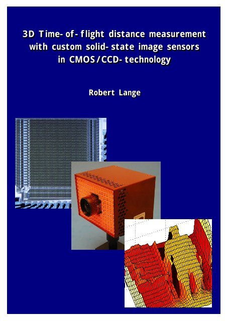
3D Time-of-flight distance measurement with custom - Universität ...
3D Time-of-flight distance measurement with custom - Universität ...
3D Time-of-flight distance measurement with custom - Universität ...

Create successful ePaper yourself
Turn your PDF publications into a flip-book with our unique Google optimized e-Paper software.
<strong>3D</strong> <strong>Time</strong>-<strong>of</strong>-<strong>flight</strong> <strong>distance</strong> <strong>measurement</strong><br />
<strong>with</strong> <strong>custom</strong> solid-state image sensors<br />
in CMOS/CCD-technology<br />
Robert Lange
<strong>3D</strong> <strong>Time</strong>-<strong>of</strong>-Flight Distance Measurement<br />
<strong>with</strong> Custom Solid-State Image Sensors in<br />
CMOS/CCD-Technology<br />
A dissertation submitted to the<br />
DEPARTMENT OF ELECTRICAL ENGINEERING AND<br />
COMPUTER SCIENCE AT UNIVERSITY OF SIEGEN<br />
for the degree <strong>of</strong><br />
DOCTOR OF TECHNICAL SCIENCES<br />
presented by<br />
Dipl.-Ing. Robert Lange<br />
born March 20, 1972<br />
accepted on the recommendation <strong>of</strong><br />
Pr<strong>of</strong>. Dr. R. Schwarte, examiner<br />
Pr<strong>of</strong>. Dr. P. Seitz, co-examiner<br />
Submission date: June 28, 2000<br />
Date <strong>of</strong> oral examination: September 8, 2000
To my parents
<strong>3D</strong> Distanzmessung nach dem<br />
„<strong>Time</strong>-<strong>of</strong>-Flight“- Verfahren mit<br />
kundenspezifischen Halbleiterbildsensoren<br />
in CMOS/CCD Technologie<br />
VOM FACHBEREICH ELEKTROTECHNIK UND INFORMATIK<br />
DER UNIVERSITÄT-GESAMTHOCHSCHULE SIEGEN<br />
zur Erlangung des akademischen Grades<br />
DOKTOR DER INGENIEURWISSENSCHAFTEN<br />
(DR.-ING.)<br />
genehmigte Dissertation<br />
vorgelegt von<br />
Dipl.-Ing. Robert Lange<br />
geboren am 20. März 1972<br />
1. Gutachter: Pr<strong>of</strong>. Dr.-Ing. R. Schwarte<br />
2. Gutachter: Pr<strong>of</strong>. Dr. P. Seitz<br />
Vorsitzender der Prüfungskommission: Pr<strong>of</strong>. Dr.-Ing H. Roth<br />
Tag der Abgabe: 28. Juni 2000<br />
Tag der mündlichen Prüfung: 8. September 2000
Meinen Eltern
Contents<br />
Contents .................................................................................................................... I<br />
Abstract ....................................................................................................................V<br />
Kurzfassung............................................................................................................IX<br />
1. Introduction.......................................................................................................... 1<br />
2. Optical TOF range <strong>measurement</strong> ....................................................................... 9<br />
2.1 Overview <strong>of</strong> range <strong>measurement</strong> techniques.......................................... 11<br />
2.1.1 Triangulation ................................................................................... 11<br />
2.1.2 Interferometry.................................................................................. 13<br />
2.1.3 <strong>Time</strong>-<strong>of</strong>-<strong>flight</strong> ................................................................................... 16<br />
2.1.4 Discussion....................................................................................... 24<br />
2.2 Measuring a signal’s amplitude and phase ............................................. 26<br />
2.2.1 Demodulation and sampling ........................................................... 26<br />
2.2.2 Aliasing ........................................................................................... 36<br />
2.2.3 Influence <strong>of</strong> system non-linearities ................................................. 46<br />
2.2.4 Summary......................................................................................... 47<br />
3. Solid-state image sensing ................................................................................ 49<br />
3.1 Silicon properties for solid-state photo-sensing....................................... 52<br />
3.1.1 Photodiodes in CMOS .................................................................... 52<br />
3.1.2 MOS photogate............................................................................... 57<br />
3.1.3 Transport mechanisms for charge carriers ..................................... 62<br />
3.1.4 Noise sources ................................................................................. 68<br />
3.1.5 Sensitivity and Responsivity ........................................................... 71<br />
3.1.6 Optical fill factor .............................................................................. 72<br />
3.2 Charge coupled devices: CCD - basic principles .................................... 73<br />
3.3 Active pixel sensors: CMOS APS............................................................ 81<br />
3.4 Discussion ............................................................................................... 83<br />
I
II<br />
4. Power budget and resolution limits................................................................. 85<br />
4.1 Optical power budget............................................................................... 85<br />
4.2 Noise limitation <strong>of</strong> range accuracy........................................................... 90<br />
5. Demodulation pixels in CMOS/CCD................................................................. 99<br />
5.1 Pixel concepts ....................................................................................... 102<br />
5.1.1 Multitap lock-in CCD ..................................................................... 102<br />
5.1.2 4-tap lock-in pixel.......................................................................... 104<br />
5.1.3 1-tap lock-in pixel.......................................................................... 109<br />
5.1.4 Summary: Geometry and speed performance.............................. 113<br />
5.2 Characterization <strong>of</strong> 1-tap pixel performance.......................................... 116<br />
5.2.1 Charge to voltage conversion ....................................................... 116<br />
5.2.2 Measurement setup, expectations and predictions ...................... 120<br />
5.2.3 Determination <strong>of</strong> optimal control voltages..................................... 130<br />
5.2.4 Influence <strong>of</strong> optical power and integration time @ 20 MHz .......... 134<br />
5.2.5 Demodulation contrast versus frequency and wavelength ........... 137<br />
5.2.6 Phase accuracy <strong>measurement</strong>s ................................................... 139<br />
5.2.7 Noise performance and dynamic range........................................ 142<br />
5.2.8 Comparison <strong>of</strong> measured <strong>distance</strong> accuracy <strong>with</strong> theory ............. 143<br />
5.2.9 Summary....................................................................................... 145<br />
5.3 Outlook: Two-photosite demodulation pixel .......................................... 147
6. Imaging TOF range cameras .......................................................................... 151<br />
6.1 Camera electronics................................................................................ 152<br />
6.1.1 Digital sequencer board................................................................ 152<br />
6.1.2 Driving electronics board .............................................................. 155<br />
6.1.3 Modulated illumination .................................................................. 158<br />
6.2 2D range camera................................................................................... 159<br />
6.2.1 108 pixel lock-in line sensor.......................................................... 159<br />
6.2.2 System architecture ...................................................................... 163<br />
6.2.3 2D range <strong>measurement</strong> ................................................................ 167<br />
6.3 <strong>3D</strong> range camera................................................................................... 169<br />
6.3.1 64 x 25 pixel lock-in image sensor................................................ 169<br />
6.3.2 System architecture ...................................................................... 171<br />
6.3.3 <strong>3D</strong> range <strong>measurement</strong> ................................................................ 173<br />
6.4 Discussion ............................................................................................. 180<br />
7. Summary and Perspective.............................................................................. 181<br />
8. Appendix .......................................................................................................... 187<br />
8.1 Physical constants................................................................................. 187<br />
8.2 Typical parameters <strong>of</strong> a 2 µm CMOS technology.................................. 188<br />
8.3 Conversion: LUMEN, WATT and CANDELA......................................... 189<br />
8.4 Measurement conditions (MCD) for Chapter 5...................................... 191<br />
References ........................................................................................................... 195<br />
Acknowledgments............................................................................................... 203<br />
Curriculum Vitae.................................................................................................. 205<br />
III
Abstract<br />
Since we are living in a three-dimensional world, an adequate description <strong>of</strong> our<br />
environment for many applications includes the relative position and motion <strong>of</strong> the<br />
different objects in a scene. Nature has satisfied this need for spatial perception by<br />
providing most animals <strong>with</strong> at least two eyes. This stereo vision ability is the basis<br />
that allows the brain to calculate qualitative depth information <strong>of</strong> the observed<br />
scene. Another important parameter in the complex human depth perception is our<br />
experience and memory. Although it is far more difficult, a human being is even<br />
able to recognize depth information <strong>with</strong>out stereo vision. For example, we can<br />
qualitatively deduce the <strong>3D</strong> scene from most photos, assuming that the photos<br />
contain known objects [COR].<br />
The acquisition, storage, processing and comparison <strong>of</strong> such a huge amount <strong>of</strong><br />
information requires enormous computational power - <strong>with</strong> which nature fortunately<br />
provides us. Therefore, for a technical implementation, one should resort to other<br />
simpler <strong>measurement</strong> principles. Additionally, the qualitative <strong>distance</strong> estimates <strong>of</strong><br />
such knowledge-based passive vision systems can be replaced by accurate range<br />
<strong>measurement</strong>s.<br />
Imaging <strong>3D</strong> <strong>measurement</strong> <strong>with</strong> useful <strong>distance</strong> resolution has mainly been realized<br />
so far <strong>with</strong> triangulation systems, either passive triangulation (stereo vision) or<br />
active triangulation (e.g. projected fringe methods). These triangulation systems<br />
have to deal <strong>with</strong> shadowing effects and ambiguity problems (projected fringe),<br />
which <strong>of</strong>ten restrict the range <strong>of</strong> application areas. Moreover, stereo vision cannot<br />
be used to measure a contrastless scene. This is because the basic principle <strong>of</strong><br />
stereo vision is the extraction <strong>of</strong> characteristic contrast-related features <strong>with</strong>in the<br />
observed scene and the comparison <strong>of</strong> their position <strong>with</strong>in the two images. Also,<br />
extracting the <strong>3D</strong> information from the measured data requires an enormous timeconsuming<br />
computational effort. High resolution can only be achieved <strong>with</strong> a<br />
relatively large triangulation base and hence large camera systems.<br />
V
VI<br />
A smarter range <strong>measurement</strong> method is the TOF (<strong>Time</strong>-Of-Flight) principle, an<br />
optical analogy to a bat’s ultrasonic system rather than human’s stereo vision. So<br />
far TOF systems are only available as 1D systems (point <strong>measurement</strong>), requiring<br />
laser scanners to acquire <strong>3D</strong> images. Such TOF scanners are expensive, bulky,<br />
slow, vibration sensitive and therefore only suited for restricted application fields.<br />
In this dissertation an imaging, i.e. non-scanning TOF-camera is introduced, based<br />
on an array <strong>of</strong> demodulation pixels, where each pixel can measure both the<br />
background intensity and the individual arrival time <strong>of</strong> an RF-modulated (20 MHz)<br />
scene illumination <strong>with</strong> an accuracy <strong>of</strong> a few hundreds <strong>of</strong> picoseconds (300⋅10 -12 s).<br />
The pixel’s working concept is based on the CCD principle (Charge Coupled<br />
Device), allowing the transportation, storage and accumulation <strong>of</strong> optically<br />
generated charge carriers to defined local sites <strong>with</strong>in the imaging device. This<br />
process is extremely fast and essentially loss-free. We call our new, powerful highfunctionality<br />
pixels demodulation pixels because they extract the target’s <strong>distance</strong><br />
and reflectivity from the received optical signal. This extracted information is<br />
modulated into the active optical signal during the time <strong>of</strong> propagation <strong>of</strong> the light<br />
(or time <strong>of</strong> <strong>flight</strong>) through the observed scene. Each pixel works like an individual<br />
high-precision stopwatch, and since its realization is mainly based on CMOS<br />
technology this new technique will benefit from the ongoing technology<br />
developments in terms <strong>of</strong> improved time- and hence <strong>distance</strong> resolution. Thanks to<br />
the use <strong>of</strong> CMOS, all commonly known CMOS APS (Active Pixel Sensor) features<br />
(Regions Of Interest addressing: ROI, AD conversion, etc.) can be implemented<br />
monolithically in the future.<br />
The imaging devices have been fabricated in a 2 µm CMOS/CCD process, a<br />
slightly modified CMOS process which is available as an inexpensive prototyping<br />
service (Multi Project Wafer: MPW). This process <strong>of</strong>fers the freedom to implement<br />
CCDs <strong>with</strong> sufficiently good performance for our application, although the<br />
performance is inferior to dedicated CCD technologies. We have realized and<br />
characterized several different pixel structures and will present these results here.<br />
The demodulation pixel <strong>with</strong> the best fill-factor and demodulation performance has<br />
been implemented (1) as a line sensor <strong>with</strong> 108 pixels and (2) as an image sensor<br />
<strong>with</strong> 64 x 25 pixels. Both devices have been integrated in separate range cameras<br />
working <strong>with</strong> modulated LED illumination and covering a <strong>distance</strong> range <strong>of</strong> 7.5 up to<br />
15 meters. For non-cooperative diffusely reflecting targets these cameras achieve
centimeter accuracy. With the single exception <strong>of</strong> the demodulation pixel array<br />
itself, only standard electronic and optical components have been used in these<br />
range cameras. For a resolution <strong>of</strong> 5 centimeters, an optical power <strong>of</strong> 600 fW per<br />
pixel is sufficient, assuming an integration time <strong>of</strong> 50 ms (20 Hz frame rate <strong>of</strong> <strong>3D</strong><br />
images). This low optical power implies that only 0.06 electrons are generated per<br />
modulation period (Tmod=50 ns at 20 MHz modulation frequency).<br />
Furthermore, we present an in-depth analysis <strong>of</strong> the influences <strong>of</strong> non-linearities in<br />
the electronics, aliasing effects, integration time and modulation functions. Also, an<br />
optical power budget and a prediction for the range accuracy is derived as a<br />
function <strong>of</strong> the ratio <strong>of</strong> active illumination to background illumination. The validity <strong>of</strong><br />
this equation is confirmed by both computer simulations and experimental<br />
<strong>measurement</strong>s <strong>with</strong> real devices. Thus, we are able to predict the range accuracy<br />
for given integration time, optical power, target <strong>distance</strong> and reflectance.<br />
With this work we demonstrate the first successful realization <strong>of</strong> an all-solid-state<br />
<strong>3D</strong> TOF range-camera <strong>with</strong>out moving parts that is based on a dedicated<br />
<strong>custom</strong>ized PhotoASIC. The measured performance is very close to the theoretical<br />
limits. We clearly demonstrate that optical <strong>3D</strong>-TOF is an excellent, cost-effective<br />
tool for all modern vision problems, where the relative position or motion <strong>of</strong> objects<br />
need to be monitored.<br />
VII
Kurzfassung<br />
Da wir in einer dreidimensionalen Welt leben, erfordert eine geeignete<br />
Beschreibung unserer Umwelt für viele Anwendungen Kenntnis über die relative<br />
Position und Bewegung der verschiedenen Objekte innerhalb einer Szene. Die<br />
daraus resultierende Anforderung räumlicher Wahrnehmung ist in der Natur<br />
dadurch gelöst, daß die meisten Tiere mindestens zwei Augen haben. Diese<br />
Fähigkeit des Stereosehens bildet die Basis dafür, daß unser Gehirn qualitative<br />
Tiefeninformationen berechnen kann. Ein anderer wichtiger Parameter innerhalb<br />
des komplexen menschlichen <strong>3D</strong>-Sehens ist unser Erinnerungsvermögen und<br />
unsere Erfahrung. Der Mensch ist sogar in der Lage auch ohne Stereosehen<br />
Tiefeninformation zu erkennen. Beispielsweise können wir von den meisten Photos,<br />
vorausgesetzt sie bilden Objekte ab, die wir bereits kennen, die <strong>3D</strong> Information im<br />
Kopf rekonstruieren [COR].<br />
Die Aufnahme, Speicherung, Weiterverarbeitung und der Vergleich dieser riesigen<br />
Datenmengen erfordert eine enorme Rechenleistung. Glücklicherweise stellt uns<br />
die Natur diese Rechenleistung zur Verfügung. Für eine technische Realisierung<br />
sollten wir aber nach einfacheren und genaueren Meßprinzipien suchen.<br />
Bildgebende <strong>3D</strong> Meßmethoden mit einer brauchbaren Distanzauflösung sind bisher<br />
nur in Form von passiven (z.B. Stereosehen) oder aktiven (z.B. Streifenprojektionsverfahren)<br />
Triangulationssystemen realisiert worden. Solche Triangulationssysteme<br />
bringen vor allem die Nachteile der Abschattungsproblematik und der Mehrdeutigkeit<br />
(Streifenprojektion) mit sich. Somit sind <strong>of</strong>tmals die möglichen Einsatzgebiete<br />
eingeschränkt. Außerdem erfordert Stereosehen kontrastreiche Szenen, denn sein<br />
Grundprinzip besteht in der Extrahierung bestimmter signifikanter (kontrastreicher)<br />
Merkmale innerhalb der Szenen und dem Positionsvergleich dieser Merkmale in<br />
den beiden Bildern. Überdies erfordert die Gewinnung der <strong>3D</strong> Information einen<br />
hohen Rechenaufwand. Hohe Meßauflösung hingegen kann man nur mit einer<br />
großen Triangulationsbasis gewährleisten, welche wiederum zu großen<br />
Kamerasystemen führt.<br />
IX
X<br />
Eine elegantere Methode zur Entfernungsmessung ist das „<strong>Time</strong>-<strong>of</strong>-Flight (TOF)“-<br />
Verfahren (Fluglaufzeitverfahren), ein optisches Analogon zum Ultraschall<br />
Navigationssystem der Fledermaus. Bisher wird das TOF- Verfahren nur eindimensional<br />
eingesetzt, also für die Distanzbestimmung zwischen zwei Punkten. Um mit<br />
solchen 1D Meßsystemen die <strong>3D</strong> Information der Szene zu erlangen, benutzt man<br />
Laserscanner. Diese sind aber teuer, groß, verhältnismäßig langsam und<br />
empfindlich gegen Erschütterungen und Vibrationen. Scannende TOF- Systeme<br />
sind daher nur für eine eingeschränkte Anzahl von Applikationen geeignet.<br />
In dieser Dissertation stellen wir erstmals eine nicht scannende bildgebende <strong>3D</strong>-<br />
Kamera vor, die nach dem TOF- Prinzip arbeitet und auf einem Array von<br />
sogenannten Demodulationspixeln beruht. Jedes dieser Pixel ermöglicht sowohl die<br />
Messung der Hintergrundintensität als auch die individuelle Ankunftszeit einer HFmodulierten<br />
Szenenbeleuchtung mit einer Genauigkeit von wenigen hundert<br />
Pikosekunden. Das Funktionsprinzip der Pixel basiert auf dem CCD Prinzip<br />
(Charge Coupled Device), welches den Transport, die Speicherung und die<br />
Akkumulation optisch generierter Ladungsträger in definierten örtlich begrenzten<br />
Gebieten auf dem Bildsensor erlaubt. Ladungstransport und -addition können von<br />
CCDs enorm schnell und beinahe verlustfrei durchgeführt werden. Wir bezeichnen<br />
diese neuartigen, hochfunktionalen und leistungsstarken Pixel als Demodulationspixel,<br />
weil man mit jedem von ihnen die Entfernungs- und Reflektivitätsinformation<br />
des zu vermessenden Ziels aus dem empfangenen optischen Signal extrahieren<br />
kann. Die gesuchte Information wird dem aktiven optischen Signal während der<br />
Ausbreitung des Lichts durch die Szene (<strong>Time</strong> <strong>of</strong> Flight) aufmoduliert. Jedes Pixel<br />
arbeitet wie eine individuelle Hochpräzisions- Stoppuhr. Da die Realisierung im<br />
wesentlichen auf CMOS- Technologie basiert, wird diese neue Technik von den<br />
stetig fortschreitenden Technologieentwicklungen und -verbesserungen pr<strong>of</strong>itieren<br />
und zwar in Form von besserer Zeitauflösung und damit höherer<br />
Distanzgenauigkeit. Dank der Benutzung einer CMOS- Technologie können<br />
zukünftig sehr leicht auch alle bekannten CMOS-APS- Eigenschaften (Active Pixel<br />
Sensor) monolithisch implementiert werden (z.B. Definition und Auslese von<br />
Bildsegmenten: regions <strong>of</strong> interest, A/D Wandlung auf dem Sensor, …).<br />
Die neuen Bildsensoren sind in einem 2 µm CMOS/CCD Prozess hergestellt<br />
worden, einem leicht modifizierten CMOS Prozess, der zur kostengünstigen<br />
Prototypenfertigung zur Verfügung steht (sogenannte MPWs, Multi Project Wafer).
Dieser Prozess bietet die Möglichkeit, CCD Strukturen zu realisieren. Obwohl diese<br />
CCDs nicht die Qualität spezieller CCD- Prozesse erreichen, genügen sie den<br />
Anforderungen unserer Anwendung vollkommen. Wir haben verschiedene<br />
Pixelstrukturen realisiert und charakterisiert und präsentieren in dieser Arbeit die<br />
Ergebnisse. Das Demodulationspixel mit dem besten Füllfaktor und den<br />
effizientesten Demodulationseigenschaften wurde als Zeilensensor mit 108 Pixeln<br />
und als Bildsensor mit 64 x 25 Pixeln fabriziert. Beide Sensoren sind in separaten<br />
Entfernungskameras implementiert, die jeweils modulierte LEDs als Lichtquelle<br />
benutzen und einen Entfernungsbereich von 7.5 Metern oder sogar 15 Metern<br />
abdecken. Für nicht kooperative diffus reflektierende Ziele erreichen beide<br />
Kameras eine Auflösung von wenigen Zentimetern. Mit Ausnahme der<br />
Bildsensoren werden in den Distanzkameras ausschließlich optische und<br />
elektrische Standardkomponenten eingesetzt. Bei einer Integrationszeit von 50 ms<br />
(20 Hz <strong>3D</strong>-Bild-Wiederholrate) genügt für eine Distanzauflösung von 5 Zentimetern<br />
eine optische Leistung von 600 Femtowatt pro Pixel (Wellenlänge des Lichts:<br />
630 nm). Bei dieser niedrigen optischen Leistung werden statistisch lediglich 0.06<br />
Elektronen innerhalb einer Modulationsperiode von 50 ns akkumuliert (20 MHz<br />
Modulationsfrequenz), also nur ein Elektron in jeder 16ten Periode.<br />
Wir führen eine ausführliche Analyse der Einflüsse von Nichtlinearitäten innerhalb<br />
der Elektronik, von Aliasing Effekten, von der Integrationszeit und von den<br />
Modulationssignalen durch. Außerdem stellen wir eine optische Leistungsbilanz auf<br />
und präsentieren eine Formel zur Voraussage der Distanzauflösung als Funktion<br />
des Verhältnisses der Hintergrundhelligkeit zur Intensität des aktiven optischen<br />
Signals sowie weiteren Kamera- und Szenenparametern. Die Gültigkeit dieser<br />
Formel wird durch Simulationen und echte Messungen verifiziert, so daß wir in der<br />
Lage sind, für eine vorgegebene Integrationszeit, optische Leistung und Zieldistanz<br />
und -reflektivität die Meßgenauigkeit des Systems vorherzusagen.<br />
Wir demonstrieren die ersten erfolgreichen Realisierungen bildgebender, rein elektronischer<br />
<strong>3D</strong>-Entfernungskameras nach dem Laufzeitprinzip ohne bewegte Teile,<br />
welche auf kundenspezifischen PhotoASICS beruhen. Die erzielten Meßresultate<br />
dieser Kameras sind beinahe ausschließlich vom natürlichen Quantenrauschen das<br />
Lichts limitiert. Wir zeigen, daß das optische <strong>3D</strong> TOF- Verfahren ein exzellentes<br />
kostengünstiges Werkzeug für alle modernen berührungslosen optischen Meßaufgaben<br />
zur Überwachung relativer Objektpositionen oder -bewegungen ist.<br />
XI
INTRODUCTION 1<br />
1. Introduction<br />
One can find time-<strong>of</strong>-<strong>flight</strong> <strong>measurement</strong> systems in nature’s navigation solutions<br />
for dolphins and bats, which use this sensor system for both navigation and object<br />
tracking (hunting). Moreover, humans have also used TOF techniques since a long<br />
time, for example by dropping rocks down deep holes and waiting for the echo or<br />
by trying to estimate the <strong>distance</strong> <strong>of</strong> a lightning discharge by evaluating the time<br />
delay between the lightning and the associated thunder. These TOF methods are<br />
based on the propagation time <strong>of</strong> sound [STR].<br />
Figure 1.1 Galileo Galilei’s experiment <strong>of</strong> the early 17 th century to prove that light<br />
travels through free space rather than existing instantaneously [HOF].<br />
The actual pioneer in optical time-<strong>of</strong>-<strong>flight</strong> <strong>measurement</strong> was Galileo Galilei, who<br />
was probably the first to imagine light as a kind <strong>of</strong> active event, something that<br />
travels through free space rather than existing instantaneously. He also tried to<br />
prove his idea by a simple experiment, described in one <strong>of</strong> his “Discorsi” that he<br />
wrote under house arrest in the early 17 th century. In the dark <strong>of</strong> night he placed two<br />
men (A and B) onto two neighboring hills, about 1 kilometer away from each other.<br />
Each <strong>of</strong> them carried a lantern, covered by their hands, so that one could not see<br />
the other’s lantern light initially. The experiment started <strong>with</strong> person A uncovering<br />
his lantern and waiting for B to uncover his lantern as well, as soon as he saw the
2 CHAPTER 1<br />
first lantern’s light (c.f. Figure 1.1). That way Galilei hoped to measure the<br />
propagation time that the light needed to travel from person A to person B and back<br />
to A, a hopeless attempt from today’s point <strong>of</strong> view, since we know that the light<br />
only needs 6.6 microseconds to travel the <strong>distance</strong> <strong>of</strong> 2 kilometers. So much more<br />
remarkable is Galilei’s conclusion from this experience. We know that Galilei was<br />
an excellent engineer: Before carrying out his experiment, he trained the<br />
experimenters to react quickly and measured their reaction times. He found that the<br />
measured speed <strong>of</strong> light was <strong>of</strong> the same order <strong>of</strong> magnitude as the reaction times<br />
that he had previously measured. Therefore, he concluded that either light exists<br />
instantaneously, as physics has taught previously, or that it propagates so<br />
incredibly quickly that it was not possible to measure its speed <strong>with</strong> the proposed<br />
experiment. A little later, in 1676 it was Roemer who succeeded in measuring the<br />
speed <strong>of</strong> light by using the departures from predicted eclipse times <strong>of</strong> a Jupiter<br />
moon, strictly speaking also a TOF experiment.<br />
It was only 200 years later, in1849, that Fizeau was more successful in measuring<br />
the time <strong>of</strong> <strong>flight</strong> on earth. He built a more precise, more mature and complicated<br />
experimental setup (illustrated in Figure 1.2) in the suburbs <strong>of</strong> Paris. Fizeau used a<br />
rotating cogwheel as a mechanical shutter for a focused light beam. This pulsed<br />
beam was projected onto a mirror, located 8633 m away. For an appropriate<br />
rotation speed <strong>of</strong> the cogwheel the complete light packet, which had been<br />
transmitted by a gap in the wheel was obstructed by a tooth after being reflected by<br />
the distant mirror, so that it could not be seen behind the cogwheel. As the <strong>distance</strong><br />
and the shutter rate (rotation period divided by the number <strong>of</strong> teeth) were known,<br />
Fizeau could calculate the speed <strong>of</strong> light. With this early TOF experiment he<br />
obtained an astonishingly precise result <strong>of</strong> 3.153⋅10 8 m/s.
INTRODUCTION 3<br />
light source<br />
observer<br />
lens<br />
lens<br />
beam splitter<br />
rotating<br />
cogwheel<br />
lens<br />
lens<br />
plane<br />
mirror<br />
Figure 1.2 Fizeau’s experimental setup used to determine the speed <strong>of</strong> light<br />
in 1849.<br />
Today, the speed <strong>of</strong> light (c=λ⋅ν) can be determined much more precisely, for<br />
example by the simultaneous <strong>measurement</strong> <strong>of</strong> frequency ν and wavelength λ <strong>of</strong> a<br />
stabilized helium-neon-laser or by the frequency <strong>measurement</strong> <strong>of</strong> an<br />
electromagnetic wave in a cavity resonator [BRK]. Since 1983 the speed <strong>of</strong> light<br />
has been fixed by definition to c=2.99792458⋅10 8 m/s. With this precise knowledge<br />
<strong>of</strong> the velocity <strong>of</strong> light, it is thus possible to modify Galilei’s or Fizeau’s experiments<br />
and to measure <strong>distance</strong>s. This can be done “simply” by measuring the elapsed<br />
time during which light travels from a transmitter to the target to be measured and<br />
back to the receiver, as illustrated in Figure 1.3. In practice, the active light source<br />
and the receiver are located very close to each other. This facilitates a compact<br />
setup and avoids shadowing effects.
4 CHAPTER 1<br />
<strong>3D</strong> object<br />
transmitter<br />
detector<br />
STOP<br />
80<br />
70<br />
60<br />
90<br />
100<br />
ns<br />
ns<br />
50<br />
"ns stop watch"<br />
10<br />
40<br />
20<br />
30<br />
receiver<br />
Figure 1.3 Basic principle <strong>of</strong> an (optical) TOF ranging system.<br />
START<br />
DISTANCE<br />
1m = 6.67ns<br />
The basic principle can be summarized as follows: A source emits a light pulse and<br />
starts a highly accurate stopwatch. The light pulse travels to the target and back.<br />
Reception <strong>of</strong> the light pulse by the detector mechanism stops the stopwatch, which<br />
now shows the time <strong>of</strong> <strong>flight</strong> <strong>of</strong> the light pulse. Considering the fact that the light<br />
pulse travels the <strong>distance</strong> twice (forth and back), a measured time <strong>of</strong> 6.67 ns<br />
corresponds to a <strong>distance</strong> <strong>of</strong> one meter. An essential property <strong>of</strong> this setup is the<br />
fact that emitter and detector are synchronous. At this point one can recognize a<br />
significant advantage <strong>of</strong> time-<strong>of</strong>-<strong>flight</strong> over a triangulation based ranging system:<br />
The TOF ranging technique does not produce incomplete range data (no shadow<br />
effects) because illumination and observation directions are collinear. It is obvious<br />
that the basic problem <strong>of</strong> establishing a TOF-ranging system is the realization <strong>of</strong> a<br />
high accuracy time-<strong>measurement</strong> mechanism. For a resolution <strong>of</strong> 1cm, an accuracy<br />
<strong>of</strong> better than 70 picoseconds is required. The stringent requirements for the<br />
receiver are one reason that, although already in 1903 Hulsmeyer carried out some<br />
experiments <strong>with</strong> electromagnetic radar, only in 1968 was Koechner one <strong>of</strong> the first<br />
to introduce an optical TOF ranging system [KOE]. Another problem was the lack <strong>of</strong><br />
high power (laser-) light sources. All these TOF ranging systems actually only<br />
measure the <strong>distance</strong> to a point (1D). In order to gain <strong>3D</strong> information, the laser<br />
beam has to be scanned over the scene in two directions. This requires high<br />
accuracy laser scanners, which are mostly bulky and sensitive to vibrations.
INTRODUCTION 5<br />
Propagation time, however, is not the only property <strong>of</strong> light that is important for this<br />
dissertation. In the early 1900’s another property <strong>of</strong> light was discovered, the socalled<br />
photoelectric effect. This is the ability <strong>of</strong> light to interact <strong>with</strong> matter, either<br />
liberating electrons from a metal plate, for example (external photoelectric effect or<br />
photoemission) or generating electron-hole pairs in semiconductor materials<br />
(internal photoelectric effect or photoconduction). Both effects can be explained by<br />
quantum physics. Albert Einstein as the first to understand the external<br />
photoelectric effect earned the Nobel Price for his explanation.<br />
The discovery <strong>of</strong> this photoelectric effect opened the doors to electronic image<br />
sensing. Already in 1939 the first electronic imaging devices, so called Orthicons<br />
(later Vidikons), were introduced. They are based on electron tubes and have been<br />
gradually replaced by solid-state cameras <strong>with</strong> the introduction <strong>of</strong> the CCD (Charge<br />
Coupled Device) in 1971 [BOY, AME]. This all-solid-state imaging device has<br />
dominated the optoelectronic market for more than two decades now. Only in the<br />
last few years has CMOS (Complementary Metal Oxide Semiconductor) technology<br />
definitely entered the imaging market [FOS]. This technology, mainly driven by the<br />
computer industry, is not only widely available and cheaper than CCD technology,<br />
the classical technology for solid-state imaging devices, but CMOS also makes it<br />
possible to implement additional functionality on-chip. Today’s CMOS sensors can<br />
<strong>of</strong>fer, for example, A/D- conversion and arbitrary access to individual pixels,<br />
enabling the definition <strong>of</strong> ROI’s (Regions Of Interest) [BLC]. In contrast to CCDs,<br />
CMOS sensors can be operated <strong>with</strong> low voltages (130 dB) [VIZ, BLC]. CMOS APS technology is also<br />
used to realize so-called smart pixels, image sensors <strong>with</strong> special functionality,<br />
such as temporal or local convolution, stereo vision, color vision, motion detection<br />
or velocity <strong>measurement</strong>, <strong>of</strong>ten inspired by visual systems found in nature [MOI].<br />
Until the middle <strong>of</strong> the 70’s, light barriers were almost exclusively used in machine<br />
vision. Only at the end <strong>of</strong> the 70’s first video cameras entered the machine vision<br />
market; they were used for object recognition and surveillance. Semiconductor<br />
imagers emerged only in the middle <strong>of</strong> the 80’s [KAP].
6 CHAPTER 1<br />
With this dissertation, both highly interesting and powerful fields <strong>of</strong> optoelectronics<br />
are combined for the first time: TOF-range <strong>measurement</strong> and <strong>custom</strong>ized image<br />
sensors <strong>with</strong> special functionality. We demonstrate an array <strong>of</strong> monolithically<br />
integrated pixels, where each pixel contains the complete demodulating receiver <strong>of</strong><br />
the TOF system. This development represents an enormous improvement for the<br />
field <strong>of</strong> <strong>3D</strong> TOF ranging. Instead <strong>of</strong> scanning a modulated beam over the scene and<br />
serially taking point <strong>distance</strong> <strong>measurement</strong>s to combine them into a <strong>3D</strong> image, the<br />
range <strong>measurement</strong>s for all observed points in the scene are now performed in<br />
parallel by the individual pixels. The actual correlation process between the<br />
received light and the synchronous reference signal, which is the essential process<br />
to measure the time delay, is performed in each pixel, immediately after the light is<br />
detected. All other electronic components <strong>with</strong>in the following signal processing<br />
chain in the range camera system are more or less uncritical, since the high-speed<br />
demodulation process is already performed <strong>with</strong>in the detection device. This is<br />
another advantage over conventional TOF systems, in which phase drifts <strong>of</strong> the<br />
system due to temperature variations and aging <strong>of</strong> critical electrical components are<br />
a serious problem, requiring calibrating reference <strong>measurement</strong>s.<br />
This work is subdivided into seven chapters:<br />
Chapter 2 roughly compares time-<strong>of</strong>-<strong>flight</strong> <strong>measurement</strong> <strong>with</strong> the other state-<strong>of</strong>-theart<br />
<strong>measurement</strong> principles: optical interferometry and triangulation. The basic<br />
working principles will be discussed, as well as typical advantages and<br />
disadvantages. Application examples will be given. Of the huge variety <strong>of</strong> operation<br />
principles for TOF ranging, a theoretical description <strong>of</strong> homodyne TOF<strong>measurement</strong><br />
is derived, <strong>with</strong> emphasis on the relevant questions for the fourphase<br />
<strong>measurement</strong> technique used in this work. In this homodyne operation<br />
mode, the phase delay (rather than the time delay) <strong>of</strong> a modulated light wave is<br />
measured. It is shown that by demodulating the incoming modulated light, the<br />
modulation signal’s amplitude and phase can be extracted. In particular, the<br />
influence <strong>of</strong> system non-linearities, the integrative nature <strong>of</strong> natural sampling, the<br />
choice <strong>of</strong> modulation signal, the total integration time and aliasing effects are<br />
discussed in detail. It is shown that the four phase <strong>measurement</strong> technique is<br />
insensitive to 1 st and 2 nd order non-linearities and to even harmonics, assuming<br />
properly chosen integration times for the sampling points.
INTRODUCTION 7<br />
Chapter 3 gives a short overview and comparison <strong>of</strong> CCD and CMOS image<br />
sensors. It is pointed out that we have to distinguish between CCD principle and<br />
CCD technology, since the latter is only a dedicated, optimized process for large<br />
area CCD imagers. The CCD principle can also be realized in (slightly modified)<br />
CMOS processes. We have used a 2.0µm CMOS/CCD process for all monolithical<br />
implementations presented in this work. This process makes it possible to realize<br />
CCDs <strong>with</strong> a charge transfer efficiency (CTE) between 96 % and 99.6 % at 20 MHz<br />
transport frequency, depending on the number <strong>of</strong> electrons to be transported (96 %:<br />
10,000 e - , 99.6 %: 1’000’000 e - ). Dedicated CCD processes reach typical CTE<br />
values <strong>of</strong> 99.9998 % and better. In spite <strong>of</strong> the inferior CTE performance compared<br />
<strong>with</strong> a CCD process, the availability <strong>of</strong> the CCD principle <strong>of</strong>fers enormous<br />
capabilities, such as virtually noise-free single electron level signal addition or fast<br />
signal sampling. For these useful properties, which have not been demonstrated<br />
<strong>with</strong> any transistor-based CMOS circuitry so far, a fair CCD performance is<br />
sufficient. This is <strong>of</strong> essential importance for an economic product development,<br />
since (1) CMOS processes are available as Multi-Project-Wafers (MPWs) for<br />
affordable prototyping and (2) additional functionality such as A/D conversion or<br />
any kind <strong>of</strong> signal processing can easily be implemented on chip. The advantages<br />
<strong>of</strong> both CCD and CMOS will be pointed out. The chapter is completed by an<br />
overview <strong>of</strong> those characteristics <strong>of</strong> silicon images sensors in general, that are <strong>of</strong><br />
special interest for the underlying TOF-application: spectral and temporal response,<br />
optical fill factor and noise sources.<br />
Since optical TOF ranging uses active illumination, an optical power budget is very<br />
important. In Chapter 4 we show the relations between the optical power <strong>of</strong> the<br />
light source, the number <strong>of</strong> electrons generated in a pixel <strong>of</strong> the imager and the<br />
resulting output voltage swing. This budget is influenced by the power and<br />
wavelength <strong>of</strong> the light source, the color, reflectivity and <strong>distance</strong> <strong>of</strong> the illuminated<br />
and imaged surface, the choice <strong>of</strong> optics <strong>of</strong> the camera as well as the quantum<br />
efficiency, integration time and internal electrical amplification <strong>of</strong> the image sensor.<br />
Also an estimation <strong>of</strong> the resolution limit is carried out. For this calculation, the<br />
quantum noise is mainly considered as a final theoretical limitation. Together <strong>with</strong><br />
the power budget, the range accuracy can then be calculated depending on the<br />
nature <strong>of</strong> the target and the technical properties <strong>of</strong> the TOF-camera.
8 CHAPTER 1<br />
The key element <strong>of</strong> the new <strong>3D</strong>-range camera, the demodulation-pixel imager, is<br />
introduced in Chapter 5. We show that a phase delay can be measured simply by<br />
electrooptically sampling the received modulated light. After the definition and an<br />
overview <strong>of</strong> the required properties <strong>of</strong> demodulation pixels, several implemented<br />
solutions will be introduced and their working principle will be described. The pixel<br />
layout <strong>with</strong> the best performance will be treated in more detail. Characterizing<br />
<strong>measurement</strong>s will show its excellent performance even at 20 MHz modulation<br />
frequency and the influence <strong>of</strong> control signal amplitude, modulation frequency and<br />
wavelength and optical power <strong>of</strong> the modulated light source on both measured<br />
contrast and time accuracy. For an optical power <strong>of</strong> only 600 fW per pixel, where<br />
only one electron is generated, statistically speaking, every 16 th modulation period<br />
(equivalent photocurrent: 200 fA), the measured time resolution is better than 300<br />
picoseconds (modulation frequency: 20 MHz, integration time 4·12.5 ms=50 ms;<br />
20 Hz frame rate). This small amount <strong>of</strong> received radiation power is therefore<br />
sufficient for a <strong>distance</strong> resolution <strong>of</strong> better than 5 cm, i.e. 0.67 % <strong>of</strong> the<br />
unambiguous <strong>distance</strong> range <strong>of</strong> 7.5 meters. A comparison <strong>of</strong> the measured results<br />
<strong>with</strong> the theoretical limitations deduced in Chapter 4 shows an excellent fit.<br />
Based on this pixel structure, two sensor arrays, a 108-pixel line and a 64x25-pixel<br />
imager, have been implemented and build into two separate range camera<br />
systems. In Chapter 6 we describe both, the sensor implementations and the<br />
complete camera systems in detail. Finally, the first real <strong>distance</strong> <strong>measurement</strong>s<br />
carried out <strong>with</strong> these camera systems are presented. Again, the accuracy<br />
achieved agrees reasonably well <strong>with</strong> the theory. As the demodulation sensor not<br />
only delivers the phase information in every pixel but at the same time modulation<br />
amplitude and background information, the <strong>3D</strong>-camera <strong>of</strong>fers both <strong>3D</strong> images and<br />
conventional 2D gray level images.<br />
A brief summary and an assessment <strong>of</strong> future developments and possible<br />
improvements close this work.
OPTICAL TOF RANGE MEASUREMENT 9<br />
2. Optical TOF range <strong>measurement</strong><br />
The basic principles <strong>of</strong> optical range <strong>measurement</strong> techniques (1) triangulation, (2)<br />
interferometry and (3) time-<strong>of</strong>-<strong>flight</strong> are introduced in this chapter. All these<br />
techniques mostly work <strong>with</strong> light, i.e. electromagnetic radiation fields in the<br />
wavelength range <strong>of</strong> 400-1000 nanometers (visible and NIR spectrum). We present<br />
a rough description <strong>of</strong> the basic working principles. The advantages and<br />
disadvantages <strong>of</strong> each principle are discussed and some examples are also given.<br />
More detailed and broader overviews over optical ranging principles can be found<br />
in the references [KAP], [BES], [ENG], [EN2], [SC1]. Figure 2.1 shows the family<br />
tree <strong>of</strong> contactless <strong>3D</strong> shape <strong>measurement</strong> techniques.<br />
Triangulation<br />
Contactless <strong>3D</strong> shape <strong>measurement</strong>s<br />
Microwave<br />
λ = 3 - 30 mm<br />
(10 - 100 GHz)<br />
depth detection by<br />
means <strong>of</strong> geometrical<br />
angle <strong>measurement</strong><br />
Light wave<br />
λ = 0.5 - 1 µm<br />
(300 - 600 THz)<br />
Interferometry<br />
depth detection by<br />
means <strong>of</strong> optical coherent<br />
time-<strong>of</strong>-<strong>flight</strong> <strong>measurement</strong><br />
Ultrasonic wave<br />
λ = 0.1 - 1 mm<br />
(0.3 - 3 MHz)<br />
<strong>Time</strong>-<strong>of</strong>-<strong>flight</strong> (TOF)<br />
depth detection by<br />
means <strong>of</strong> optical modulation<br />
time-<strong>of</strong>-<strong>flight</strong> <strong>measurement</strong><br />
Figure 2.1 Family tree <strong>of</strong> contactless <strong>3D</strong> shape <strong>measurement</strong> [SC1].<br />
Since TOF <strong>measurement</strong> is the underlying principle <strong>of</strong> this work, it is discussed in<br />
more detail. The first part <strong>of</strong> this chapter is closed by a discussion and a<br />
comparison <strong>of</strong> the different ranging techniques. It should be mentioned that also<br />
microwave (λ=3–30 mm) and ultrasound (λ=0.1-1 mm) techniques have their<br />
application-specific advantages. However, they are not included in this comparison.<br />
Due to diffraction limitations, both techniques are not suited for range<br />
<strong>measurement</strong>s <strong>with</strong> high angular resolution, at an acceptable size <strong>of</strong> the
10 CHAPTER 2<br />
<strong>measurement</strong> system. They find their applications in differential GPS or synthetic<br />
aperture radar (SAR) [SC1].<br />
Out <strong>of</strong> a large variety <strong>of</strong> modulation techniques for TOF, homodyne phase-shift<br />
modulation is chosen for the operation <strong>of</strong> the ranging sensors introduced in this<br />
work. Therefore, in the second part <strong>of</strong> this chapter, the equations will be derived for<br />
the four-phase realization <strong>of</strong> homodyne modulation. We show that sampling is<br />
always also a correlation process and analyze theoretically the influences <strong>of</strong><br />
sampling interval, modulation signal and integration time on the result <strong>of</strong><br />
demodulation and the system performance. Aliasing effects are discussed and it is<br />
shown that 1 st and 2 nd order non-linearities and even harmonics have no influence<br />
on the four-phase algorithm.
OPTICAL TOF RANGE MEASUREMENT 11<br />
2.1 Overview <strong>of</strong> range <strong>measurement</strong> techniques<br />
2.1.1 Triangulation<br />
This ranging technique has been known and used by nature for millions <strong>of</strong> years. It<br />
is, in the form <strong>of</strong> stereo-vision together <strong>with</strong> the depth-<strong>of</strong>-focus system (which so to<br />
speak also belongs to triangulation systems), the basis for human depth perception.<br />
Triangulation is a geometrical approach, where the target is one point <strong>of</strong> a triangle<br />
whose two remaining points are known parts <strong>of</strong> the <strong>measurement</strong> system. The<br />
<strong>distance</strong> <strong>of</strong> the target can then be determined by measuring the triangle’s angles or<br />
the triangulation base. Literature distinguishes passive and active triangulation<br />
techniques. Both principles are illustrated in Figure 2.2.<br />
Figure 2.2 Principles <strong>of</strong> passive (left) and active (right) triangulation rangefinding.<br />
Passive techniques rely on observing the same point from two different sites A and<br />
B <strong>of</strong> known <strong>distance</strong> x and measuring the viewing angles α and β <strong>with</strong> respect to<br />
the base AB. The observed point’s <strong>distance</strong> z can then be calculated using the<br />
following equation:<br />
x<br />
z =<br />
1<br />
+<br />
tan α<br />
1<br />
tan<br />
β<br />
Equation 2.1<br />
Since each point to measure must be identified from both viewing positions<br />
unambiguously, passive triangulation techniques require a scene <strong>with</strong> high contrast.<br />
Stereovision is one famous <strong>3D</strong> realization <strong>of</strong> passive triangulation [MAZ]. This<br />
technique uses at least two cameras to observe the scene from different angles.
12 CHAPTER 2<br />
Using 2D-correlation, typical object features are found and compared in both<br />
images. From the position <strong>of</strong> each feature’s centroid in both separate images, the<br />
angles α and β can be deduced and the <strong>distance</strong> can be calculated <strong>with</strong><br />
Equation 2.1, assuming that the <strong>distance</strong> <strong>of</strong> the cameras <strong>with</strong> respect to each<br />
other, as well as their orientation are known. The computational effort must not be<br />
underestimated. Shadowing effects are also typical problems <strong>with</strong> which all<br />
triangulation systems have to cope. Stereovision works pretty well for certain<br />
defined scenes, preferably chosen <strong>with</strong> rich contrast and relatively flat objects. For<br />
typical industrial scenes, however, it is <strong>of</strong>ten not suitable. Though the shadowing<br />
problem can be minimized by enlarging the number <strong>of</strong> cameras and realizing<br />
“multiple viewpoint triangulation systems”, this improvement has to be paid for by<br />
an enormous increase in computation. Nevertheless, shadowing and the need for<br />
significant contrast in the targeted scene remain a problem. Additionally, cost and<br />
overall system size, one major drawback <strong>of</strong> triangulation systems anyhow, increase<br />
<strong>with</strong> the number <strong>of</strong> cameras. Another famous member <strong>of</strong> passive triangulation<br />
systems is the theodolite.<br />
Active triangulation, as illustrated in Figure 2.2, uses a light source to project a<br />
point (in the simplest case) to the scene, which is observed by a position sensitive<br />
detector. Rather than measuring angles directly, active triangulation is based on the<br />
similarity <strong>of</strong> triangles, the object triangle and the image triangle, which is fully<br />
defined by the optical axis <strong>of</strong> the imaging device, the focal length h <strong>of</strong> the system<br />
and the position <strong>of</strong> the point projection x’ on the detector. With knowledge <strong>of</strong> the<br />
displacement x <strong>of</strong> the light source from the imaging device, the <strong>distance</strong> z <strong>of</strong> the<br />
target can be determined:<br />
x<br />
z = h ⋅<br />
x′<br />
Equation 2.2<br />
For a good <strong>distance</strong> resolution δz, small absolute <strong>distance</strong>s z, a large triangulation<br />
base x and a good local detector resolution δx’ are required. δz estimates to:<br />
2<br />
1 z<br />
δ z = ⋅ ⋅ δx′<br />
Equation 2.3<br />
h x<br />
With laser point projection, <strong>3D</strong> information can only be gained by scanning the laser<br />
point over the scene and thus sequentially acquiring a cloud <strong>of</strong> range points [RIX,<br />
BER]. A faster approach is to project a line (or light sheet) onto the <strong>3D</strong> scene. By<br />
replacing the position sensitive line sensor by an imaging array, a 2D <strong>distance</strong>
OPTICAL TOF RANGE MEASUREMENT 13<br />
pr<strong>of</strong>ile can then be measured <strong>with</strong> one shot, and for <strong>3D</strong> data the scan only needs to<br />
be performed in one direction (light sheet triangulation). In industrial inspection<br />
applications, such a 1D scan is <strong>of</strong>ten available free <strong>of</strong> cost, since the objects to<br />
measure are moving anyway, for example on an assembly-line. [KRA] presents<br />
such a scanning <strong>3D</strong> camera working <strong>with</strong> active light sheet triangulation and<br />
delivering 50 depth images per second in CCIR video format.<br />
Further advanced techniques even use 2D structured light illumination and 2D<br />
imaging to perform <strong>3D</strong> triangulation <strong>measurement</strong>s <strong>with</strong>out scanning. The most<br />
important members <strong>of</strong> this structured light group are phase shifting projected fringe,<br />
Gray code approach [BRE], phase shifting moiré [DOR], coded binary patterns,<br />
random texture [BES] or color-coded light. They typically use LCD (Liquid Crystal<br />
Display) projectors for the projection <strong>of</strong> the structured patterns.<br />
Triangulation systems are available for applications from mm-range (depth <strong>of</strong> focus)<br />
to 100km range (photogrammetry). Their main drawback is that for a good<br />
resolution they have to be large in size, since they need a large triangulation base.<br />
On the other hand, the larger this triangulation base, the more they are restricted by<br />
shadowing effects. Also, <strong>3D</strong> triangulation systems are relatively expensive since<br />
they require fast LCD projectors (only active systems) as well as large<br />
computational power.<br />
2.1.2 Interferometry<br />
Interferometry is described by the superposition <strong>of</strong> two monochromatic waves <strong>of</strong><br />
frequency ν, amplitude U1 and U2 and phase ϕ1 and ϕ2, respectively, resulting in<br />
another monochromatic wave <strong>of</strong> the same frequency ν, but <strong>with</strong> different phase and<br />
different amplitude [SAL]. In the easiest interferometer setup, the Michelson<br />
interferometer, illustrated in Figure 2.3, a laser beam (monochromatic and<br />
coherent) is split into two rays by a beam splitter. One ray is projected to a mirror <strong>of</strong><br />
constant displacement x1 (reference path) whereas the other beam is targeted on<br />
the object <strong>of</strong> variable <strong>distance</strong> x2 (<strong>measurement</strong> path). Both beams are reflected<br />
back to the beam splitter, which projects them onto an integrating detector.
14 CHAPTER 2<br />
Figure 2.3 Working principle <strong>of</strong> Michelson interferometer<br />
With the reference wave U1 and the object wave U2 defined as<br />
U1<br />
=<br />
2π⋅(<br />
2⋅x<br />
)<br />
j<br />
1<br />
I ⋅ λ<br />
1 e<br />
U2<br />
=<br />
2π⋅(<br />
2⋅x<br />
2 )<br />
j<br />
I ⋅ λ<br />
2 e<br />
(I1 and I2 are the optical intensities) we obtain the interference equation<br />
( 2 ⋅ x − 2 ⋅ x )<br />
Equation 2.4<br />
⎧2π<br />
⋅<br />
⎫<br />
I = I + + ⋅ ⋅<br />
2 1<br />
1 I2<br />
2 I1<br />
I2<br />
cos⎨<br />
⎬<br />
⎩ λ<br />
Equation 2.5<br />
⎭<br />
Note that we have to consider the double path lengths 2·x1 and 2·x2 respectively<br />
because the light waves travel the paths twice, forth and back. For equal reference<br />
and <strong>measurement</strong> path x1 and x2, as well as for path differences <strong>of</strong> exact multiples<br />
<strong>of</strong> the light’s half wavelength λ/2, the intensity on the detector reaches a maximum.<br />
This case is denoted as constructive interference. For a path difference λ/4 or<br />
n⋅λ/2 + λ/4, the intensity tends to a minimum: destructive interference.<br />
A movement <strong>of</strong> the object away from the system (or towards the system) results in<br />
an intensity peak <strong>of</strong> the interferogram (constructive interference) each time the<br />
object has moved by a multiple <strong>of</strong> the laser’s half wavelength. By recording and<br />
counting the number <strong>of</strong> minimum-maximum transitions in the interference pattern<br />
over time, when the object moves, the <strong>distance</strong> <strong>of</strong> movement can be incrementally<br />
determined at an accuracy <strong>of</strong> the light’s wavelength or even better [CRE].<br />
Interferometry therefore uses the light’s built-in scale, its wavelength, for performing
OPTICAL TOF RANGE MEASUREMENT 15<br />
highly accurate relative <strong>distance</strong> <strong>measurement</strong>s. This technique can be equivalently<br />
interpreted as a time-<strong>of</strong>-<strong>flight</strong> principle, since the runtime difference between the<br />
reference and <strong>measurement</strong> path is evaluated.<br />
Several other interferometer setups can be found, for example in [SAL] or [HEC].<br />
The principal drawback <strong>of</strong> classical interferometers is that absolute <strong>distance</strong><br />
<strong>measurement</strong>s are not possible and the unambiguous <strong>distance</strong> range is as low as<br />
half the wavelength. Enhanced approaches overcome this restriction. One nice<br />
example is Multiple-wavelength interferometry, where two very closely spaced<br />
wavelengths are used at the same time. That way beat frequencies down to GHz or<br />
even MHz range are synthetically generated, enabling absolute <strong>measurement</strong>s<br />
over several tens <strong>of</strong> centimeters at λ/100 resolution [ZIM, SC1]. Especially<br />
important for high sensitivity <strong>3D</strong> deformation <strong>measurement</strong>s is the electronic<br />
speckle pattern interferometry (ESPI), where a reference wave front interferes <strong>with</strong><br />
the speckle pattern reflected by the investigated object. With a conventional CCD<br />
camera the speckle interferogram, carrying information <strong>of</strong> the object deformation,<br />
can then be acquired. Like conventional interferometers, ESPI can also be<br />
improved in sensitivity and <strong>measurement</strong> range by the multiple-wavelength<br />
technique. [ENG]<br />
Another way to enlarge the <strong>measurement</strong> range is to use light sources <strong>of</strong> low<br />
coherence length. Such interferometers (white-light interferometry or low-coherence<br />
interferometry [BOU]) make use <strong>of</strong> the fact that only coherent light shows<br />
interference effects. If the optical path difference between the <strong>measurement</strong> and<br />
reference paths is higher than the coherence length <strong>of</strong> the light, no interference<br />
effects appear. For a path difference <strong>of</strong> the order <strong>of</strong> magnitude <strong>of</strong> the coherence<br />
length, however, interference takes place. The strength <strong>of</strong> interference, depends on<br />
the path difference between the reference and object beams, and thus absolute<br />
<strong>distance</strong>s can be measured.<br />
Interferometry finds its applications predominantly for highly accurate<br />
<strong>measurement</strong>s (λ/100 to λ/1000) over small <strong>distance</strong>s ranging from micrometers to<br />
several centimeters.
16 CHAPTER 2<br />
2.1.3 <strong>Time</strong>-<strong>of</strong>-<strong>flight</strong><br />
Similarly to interferometry, we can measure an absolute <strong>distance</strong> if we manage to<br />
measure the absolute time that a light pulse needs to travel from a target to a<br />
reference point, the detector. This indirect <strong>distance</strong> <strong>measurement</strong> is possible since<br />
we know the speed <strong>of</strong> light very precisely: c = 3⋅10 8 m/s = 2⋅150 m/µs =<br />
2⋅0.15 m/ns = 2⋅0.15 mm/ps [BRK, BRR]. In practice, the active light source and the<br />
receiver are located very closely to each other. This facilitates a compact setup and<br />
avoids shadowing effects. The basic principle <strong>of</strong> a TOF-ranging system is illustrated<br />
in Figure 1.3. A source emits a light pulse and starts a high accuracy stopwatch in<br />
the detector. The light pulse travels to the target and back. Reception <strong>of</strong> the light<br />
pulse by the detector mechanism stops the time <strong>measurement</strong> and the stopwatch<br />
now shows the time <strong>of</strong> <strong>flight</strong> <strong>of</strong> the light pulse. Considering the fact that the light<br />
pulse travels the path twice (forth and back) a measured time <strong>of</strong> 6.67 ns<br />
corresponds to a <strong>distance</strong> <strong>of</strong> 1 m and a time accuracy <strong>of</strong> better than seven<br />
picoseconds is required for a <strong>distance</strong> resolution <strong>of</strong> 1 mm. An essential property <strong>of</strong><br />
this setup is the fact that emitter and detector are operated synchronously. At this<br />
point one can already recognize a significant advantage <strong>of</strong> time-<strong>of</strong>-<strong>flight</strong> over a<br />
triangulation system: The TOF ranging technique does not produce incomplete<br />
range data (no shadow effects) because illumination and observation directions can<br />
be collinear.<br />
Also, the basic problem <strong>of</strong> establishing a TOF-ranging system is obvious here: the<br />
realization <strong>of</strong> a high accuracy time <strong>measurement</strong>. In the following subchapters<br />
different operation modes and the associated components (light source, modulator,<br />
demodulator, detector) for TOF applications are introduced.<br />
I. MODULATION SIGNALS<br />
Generally, TOF ranging systems use pulsed modulation [MOR] or continuous (CW)<br />
modulation [BEH] <strong>of</strong> the light source; combinations <strong>of</strong> both are also possible (e.g.<br />
pseudo-noise modulation). Both modulation principles have their specific<br />
advantages and disadvantages, which are treated in the following. Figure 2.4 gives<br />
an overview over the different types <strong>of</strong> modulation signals available for TOF<br />
systems.
OPTICAL TOF RANGE MEASUREMENT 17<br />
Pulsed<br />
modulation<br />
AM<br />
homodyne<br />
phase-shift<br />
Lightbeam<br />
(1D-illumination)<br />
0D-detector<br />
0D-mixer<br />
2D-scanner<br />
<strong>Time</strong>-<strong>of</strong>-<strong>flight</strong> <strong>measurement</strong><br />
AM<br />
heterodyne<br />
ZF-phase<br />
CW<br />
modulation<br />
Lightstripe<br />
(2D-illumination)<br />
1D-line-detector<br />
1D-mixer<br />
1D-scanner<br />
FM<br />
chirp<br />
modulation<br />
Pseudo-noise<br />
modulation<br />
AM<br />
+ sequential<br />
phase coding<br />
Lightvolume<br />
(<strong>3D</strong>-illumination)<br />
2D-detector-array<br />
2D-mixer<br />
No scanner<br />
Figure 2.4 Family tree <strong>of</strong> TOF modulation principles and <strong>3D</strong>-TOF realization<br />
[SC1].<br />
Pulsed modulation<br />
Pulsed light operation, as illustrated in Figure 1.3, is the most obvious method <strong>of</strong><br />
operating a TOF system, because the time <strong>of</strong> <strong>flight</strong> is measured directly. The actual<br />
time <strong>measurement</strong> is performed by correlation <strong>of</strong> a start and stop signal <strong>with</strong> a<br />
parallel running counter. The advantage <strong>of</strong> using pulsed light is the possibility <strong>of</strong><br />
transmitting a high amount <strong>of</strong> energy in a very short time. Thus the influence <strong>of</strong><br />
background illumination can be reduced and a high short-term optical signal-tonoise<br />
(and signal-to-background) ratio is attained while maintaining a low mean<br />
value <strong>of</strong> optical power. This is an important factor for eye safety, which is the<br />
limiting criterion for many <strong>measurement</strong> applications. Furthermore, it reduces the<br />
demand on a very high sensitivity and signal-to-noise ratio <strong>of</strong> the detector, thus<br />
enabling long <strong>distance</strong> <strong>measurement</strong>s. However, at the same time the receiver<br />
must <strong>of</strong>fer high dynamics and a large bandwidth. The basic problem for the<br />
receiving path is to detect exactly the arrival time <strong>of</strong> the back-scattered light pulse.
18 CHAPTER 2<br />
This is because (1) the optical threshold is not a fixed value but changes <strong>with</strong><br />
background and <strong>distance</strong> <strong>of</strong> the object, and (2) atmospheric attenuation leads to<br />
dispersion <strong>of</strong> the light pulse and flattens the slope <strong>of</strong> the received pulse. Also, it is<br />
tricky to produce very short light pulses <strong>with</strong> fast rise and fall times, which are<br />
necessary to assure an accurate detection <strong>of</strong> the incoming light pulse. Current<br />
lasers or laser diodes, the only optical elements <strong>of</strong>fering the required short pulse<br />
widths at sufficiently high optical power, still suffer from relatively low repetition<br />
rates for the pulses, which typically are in the range <strong>of</strong> some 10 kHz. Such low<br />
repetition rates drastically restrict the frame rate for TOF scanners.<br />
Nevertheless, due to the advantages gained concerning signal-to-background ratio,<br />
most <strong>of</strong> today’s TOF rangefinders are operated <strong>with</strong> pulsed modulation. [LEI, RIG]<br />
Continuous wave (CW) modulation<br />
CW-modulation <strong>of</strong>fers the possibility <strong>of</strong> using alternative modulation-, demodulationand<br />
detection-mechanisms. Compared to pulsed modulation a larger variety <strong>of</strong> light<br />
sources is available for this mode <strong>of</strong> operation because extremely fast rise and fall<br />
times are not required. Different shapes <strong>of</strong> signals are possible; sinusoidal waves or<br />
square waves are only some examples. For CW-modulation generally the phase<br />
difference between sent and received signals is measured, rather than directly<br />
measuring a light pulse’s turn-around time. As the modulation frequency is known,<br />
this measured phase directly corresponds to the time <strong>of</strong> <strong>flight</strong>, the quantity <strong>of</strong><br />
interest.<br />
The use <strong>of</strong> several modulation frequencies is known as heterodyne operation or<br />
frequency shifting [SC3]. Heterodyne mixing especially <strong>of</strong>fers the powerful<br />
possibility <strong>of</strong> synthetically generating beat frequencies. Thus the unambiguous<br />
<strong>distance</strong> range is increased while maintaining absolute accuracy. However, this<br />
requires relatively high bandwidth and linearity for both transmitting and receiving<br />
path.<br />
In this work we mainly whish to demonstrate the possibility <strong>of</strong> realizing <strong>3D</strong>-TOF <strong>with</strong><br />
<strong>custom</strong> photoASICs. Rather than examining all possible modulation modes, we<br />
focus on homodyne operation (phase shifting technique), as discussed in more<br />
detail in Chapter 2.2. The homodyne operation works <strong>with</strong> one single frequency<br />
and does not necessarily require a large bandwidth.
OPTICAL TOF RANGE MEASUREMENT 19<br />
Additionally, a large variety <strong>of</strong> intelligent CW modulation techniques is available. It<br />
is worth mentioning pseudo-random modulation and chirping (continuous frequency<br />
modulation) [XU]. Pseudo-random modulation, where pseudo noise words (PN<br />
modulation) are continuously repeated, <strong>of</strong>fers the advantage <strong>of</strong> a very high peak in<br />
the autocorrelation function. This technique, originally developed for communication<br />
technology, is therefore very noise-robust [SC2].<br />
A combination <strong>of</strong> both CW modulation and pulsed modulation would be ideal,<br />
combining their specific advantages <strong>of</strong> (1) better optical signal-to-background ratio<br />
than available from pure CW-modulation, (2) increased eye safety due to a low<br />
mean value <strong>of</strong> optical power and (3) larger freedom in choosing modulation signals<br />
and components. Combination in this content means, for example, a “pulsed sine”<br />
operation, i.e. a sequence <strong>of</strong> 1 ms high power sine modulation followed by 9 ms <strong>of</strong><br />
optical dead time. This dead time can be used for example for post processing<br />
tasks.<br />
II. COMPONENTS<br />
In the following, the necessary components for TOF systems will be described and<br />
associated <strong>with</strong> the corresponding modulation technique.<br />
Modulated light sources and electrooptical modulators<br />
The emitted light can be modulated in several ways. The use <strong>of</strong> LEDs or lasers<br />
allows direct modulation <strong>of</strong> the light source by controlling the electrical current.<br />
Since the light sent does not have to be coherent or monochromatic, other light<br />
sources are possible, in combination <strong>with</strong> additional large aperture optical<br />
modulators such as Kerr cells [HEC], Pockels cells [HEC, SC3], mechanical<br />
shutters or liquid crystal shutters. Pulsed operation <strong>with</strong> fast rise and fall times is<br />
only possible <strong>with</strong> directly controlled laser sources that allow pulses <strong>of</strong> less than ten<br />
femtoseconds [SUT]. The different light sources and modulators can be<br />
characterized in terms <strong>of</strong> light intensity, cut-<strong>of</strong>f frequency, linearity, wavelength,<br />
modulation depth (the ratio <strong>of</strong> signal amplitude to signal <strong>of</strong>fset), eye safety<br />
properties, size and price.<br />
LEDs are relatively inexpensive. They can be modulated up to some 100 MHz <strong>with</strong><br />
a 100% modulation depth and a very high linearity. They are available for a wide
20 CHAPTER 2<br />
range <strong>of</strong> wavelengths from blue (400 nm) to the near infrared (1200 nm) <strong>with</strong> an<br />
optical power <strong>of</strong> up to several milliwatts. Lasers, even laser diodes, are much more<br />
expensive than LEDs and are <strong>of</strong>ten larger. However, they <strong>of</strong>fer more optical power<br />
and are suited for operation up to some GHz, also at a wide range <strong>of</strong> wavelengths<br />
[SAL]. Practically, lasers and laser diodes are the only light sources suitable for<br />
pulsed TOF operation. All other light sources introduced here are actually used for<br />
CW modulated light, due to the reduced bandwidth requirements.<br />
Kerr cells are based on the quadratic electro-optic effect, where the polarization <strong>of</strong><br />
a polarized beam is rotated depending on the applied voltage. Together <strong>with</strong> a<br />
polarizer and a modulated control voltage <strong>of</strong> the cell, a polarized incoming beam<br />
can be modulated in intensity. Kerr cells can be used as modulators up to 10 GHz<br />
but voltages as high as 30 kV must be switched at this speed [HEC]. Pockels cells,<br />
making use <strong>of</strong> the linear electro-optic effect (pockels effect), work very similarly and<br />
also require polarized light for operation. Their cut-<strong>of</strong>f frequency <strong>of</strong> more than<br />
25 GHz is even higher than that <strong>of</strong> Kerr cells. The driving voltage requirements are<br />
a factor <strong>of</strong> 10 lower than for an equivalent Kerr cell. However, the Pockels cell still<br />
requires some kilovolts to switch from transparent to opaque mode. Therefore, the<br />
practical cut-<strong>of</strong>f frequency, which is limited by the cell’s capacitance, reaches only<br />
several hundred MHz [HEC, SAL, XU].<br />
Liquid crystal shutters are limited to some kHz <strong>of</strong> modulation frequency and are<br />
therefore not suited for high-resolution <strong>measurement</strong> applications in the 10 meter<br />
range [SAL]. An interesting alternative, however, might be the realization <strong>of</strong> a<br />
mechanical shutter. Miniaturized air turbines <strong>with</strong> a rotation speed <strong>of</strong> 427’000 rpm<br />
have been reported [SLO]. If one manages to rotate a light grating disc <strong>with</strong> such<br />
an air turbine, shutter frequencies as high as 1 MHz might become possible. For<br />
example, a disc <strong>of</strong> 10cm diameter and a slot width <strong>of</strong> 1 mm at the edge <strong>of</strong> the disc<br />
would contain about 150 slots. Such a disc would <strong>of</strong>fer a 1x1 mm 2 shutter aperture<br />
while allowing 1 MHz shutter frequency (=150*427000(1/min)/60(s/min)).<br />
Detectors and Demodulation<br />
The easiest and most straightforward way <strong>of</strong> realizing a TOF-receiver is to use any<br />
fast and sensitive electrooptical sensor as a detector. The time <strong>of</strong> <strong>flight</strong> can then be<br />
determined as follows: a linear analog ramp (or a fast digital counter) is started<br />
synchronously <strong>with</strong> the transmission <strong>of</strong> a laser pulse. Once the laser pulse reaches<br />
the detector the rise <strong>of</strong> the ramp is stopped. The resulting amplitude is then
OPTICAL TOF RANGE MEASUREMENT 21<br />
proportional to the time <strong>of</strong> <strong>flight</strong>. The difficulty <strong>of</strong> this detection mechanism is the<br />
definition <strong>of</strong> a trigger level for the detector, because the amplitude <strong>of</strong> the received<br />
light strongly depends on the <strong>distance</strong>, background and the surface to measure.<br />
For 1D-TOF ranging systems, high dynamic, high sensitivity PIN photo diodes or<br />
APDs (avalanche photo diodes) are used. PIN photo diodes have a very fast<br />
response. Typical cut-<strong>of</strong>f frequencies are 10 GHz and beyond. After the fast<br />
detection, the modulated light, now converted to an electrical signal, is electrically<br />
demodulated (using sophisticated special purpose ICs) leading to the desired<br />
phase difference between transmitter and receiver. This electrical demodulation<br />
<strong>of</strong>ten suffers from temperature drifts <strong>of</strong> the electric components involved. Therefore,<br />
regular reference <strong>measurement</strong>s and calibration are necessary to ensure<br />
reproducible <strong>measurement</strong>s. APDs and photomultiplier tubes [PAR] can be<br />
modulated in their sensitivity, enabling a direct demodulation or mixing <strong>of</strong> the<br />
incoming light. Today, TOF rangefinders and TOF laser scanners are available <strong>with</strong><br />
mm accuracy for cooperative and several cm resolution for non-cooperative targets<br />
over a <strong>distance</strong> <strong>of</strong> some 10 up to 100 meters and more [LEI, KAI].<br />
All these components only allow a 1D <strong>measurement</strong>, i.e. the <strong>distance</strong> <strong>measurement</strong><br />
<strong>of</strong> one point in the <strong>3D</strong> scene. The operation <strong>of</strong> many such receivers in parallel<br />
appears to be impractical due to large size and enormous demand on additional<br />
electronics. Therefore, 2D depth pr<strong>of</strong>iles or <strong>3D</strong> depth images can only be obtained<br />
from such 0D detectors by scanning the light beam over the observed surface.<br />
This, however, requires time, because every point has to be measured serially. It<br />
also requires mechanical scanners <strong>of</strong> very high precision. Those scanners are<br />
bulky, expensive, and sensitive to vibrations.<br />
III. <strong>3D</strong> TOF RANGING<br />
Instead <strong>of</strong> scanning a laser beam and serially acquiring the range data point-wise,<br />
we can illuminate the entire scene <strong>with</strong> a modulated light surface in order to<br />
perform a <strong>3D</strong> <strong>measurement</strong>, as illustrated in Figure 2.5. This, however,<br />
necessitates the use <strong>of</strong> a 2D-electrooptical demodulator and detector to measure<br />
the <strong>distance</strong>s <strong>of</strong> some hundreds or thousands <strong>of</strong> points <strong>of</strong> the observed scene in<br />
parallel.<br />
The 2D detection itself can be performed <strong>with</strong> CCDs or (active) photodiode arrays,<br />
so called active pixel sensors (APS). However, in contrast to discrete photodiodes,
22 CHAPTER 2<br />
these 2D detectors integrate the incoming light in every pixel and so the temporally<br />
coded information is lost. One would need to realize an electrical (de)modulator in<br />
every pixel, which demodulates the photocurrent <strong>of</strong> the pixel’s photodiode. In<br />
contrast to the 1D-case, where APD point-detectors <strong>with</strong> modulation capability can<br />
be used, for an imaging <strong>3D</strong> application such electrical 2D-demodulation devices are<br />
not available and would be hard to realize. The demodulation circuitry would have<br />
to be extremely sensitive and noise-free. Additionally, it would occupy space and<br />
thus lowers the device’s optical fill factor.<br />
<strong>3D</strong> scene<br />
Figure 2.5 Principle <strong>of</strong> a non-scanning <strong>3D</strong> TOF-camera<br />
IV. SPECIAL COMPONENTS FOR IMAGING <strong>3D</strong> TOF<br />
RF-modulated<br />
transmitter<br />
20 MHz<br />
phase<br />
RF<br />
2D-detector<br />
and 2D-<br />
RF-phase meter<br />
DISTANCE<br />
IMAGE<br />
1m = 6.67ns<br />
6.67ns = 48°<br />
What can, however, be done is to demodulate the light in the optical domain before<br />
it is detected. This can be achieved using large aperture optical modulators, such<br />
as Kerr cells or Pockels cells [SC3]. They enable the use <strong>of</strong> commercially available<br />
detector arrays (e.g. CCD or CMOS APS) for the optical to electrical conversion.<br />
There is no need for the detectors themselves to be very fast because they only<br />
integrate DC images containing the phase information (<strong>distance</strong> information,<br />
respectively), amplitude information and <strong>of</strong>fset information (background image). An<br />
interesting alternative is to use a two dimensional photomultiplier tube as optical<br />
demodulator: the so-called microchannel plate (MCP) [KA2, PHS, SAL]. An MCP<br />
can be switched on and <strong>of</strong>f in less than 500 ps (1 GHz modulation frequency).<br />
However, all these devices suffer from relatively high price and a need for elaborate<br />
electronics, since voltage amplitudes in the range <strong>of</strong> some kilovolts are necessary.<br />
A very interesting approach is the gated operation <strong>of</strong> a conventional 2D camera in<br />
combination <strong>with</strong> pulsed light. This setup has been suggested in [KAP] and [KA1],
OPTICAL TOF RANGE MEASUREMENT 23<br />
where an optical modulator works as an electrooptical shutter <strong>with</strong> varying<br />
sensitivity over time. A similar realization, making use <strong>of</strong> the built-in electronic<br />
shutter <strong>of</strong> a conventional CCD camera, rather than an additional optical modulator,<br />
is described in [DAS]. This system works as follows: A light pulse <strong>of</strong> some tens <strong>of</strong><br />
nanoseconds is transmitted by a laser and it synchronously starts the integration <strong>of</strong><br />
a standard CCD camera. With the electrical shutter mechanism <strong>of</strong> the CCD<br />
camera, only a very short period <strong>of</strong> time (also some tens <strong>of</strong> nanoseconds) is<br />
integrated. Thus, depending on the <strong>distance</strong> <strong>of</strong> the targets, only a fraction <strong>of</strong> the<br />
light pulse arrives before the integration stops. Performing two calibration<br />
<strong>measurement</strong>s, one <strong>with</strong>out laser illumination and one <strong>with</strong> non-pulsed, continuous<br />
laser illumination, enables <strong>distance</strong> calculation. However, compared to the total<br />
power consumption <strong>of</strong> nearly 200 Watts, the <strong>distance</strong> resolution <strong>of</strong> ± 20 cm for non<br />
cooperative targets in a 10 m range at 7 Hz frame rate is relatively poor. The<br />
reason for this low performance is that no repetitive integration is possible; the CCD<br />
has to be read out after every short time integration. This leads to a poor signal-tonoise<br />
ratio <strong>of</strong> this realization that can only be compensated by very high optical<br />
power <strong>of</strong> the laser. The power <strong>of</strong> laser sources, on the other hand, is limited by eye<br />
safety regulations.<br />
The restriction <strong>of</strong> conventional CCDs only allowing one short-time integration, as<br />
described above, requires innovative, smarter 2D demodulation arrays realized as<br />
<strong>custom</strong>ized PhotoASICs. The first such device, realized in CCD technology, was,<br />
however, not intended to be used in an optical ranging system but for a 2Dpolarimeter<br />
[POW]. For simplified <strong>3D</strong> TOF <strong>measurement</strong> <strong>with</strong>out mechanical<br />
scanners, the lock-in CCD sensor was invented [SP1-SP4]. Based on these lock-in<br />
structures, we present arrays <strong>of</strong> improved demodulation pixels in Chapter 5. In<br />
these pixels, CCD gates are arranged such that light generated charge carriers<br />
under the photo gate can be moved to different storage sites. This allows fast<br />
sampling <strong>of</strong> incoming light, enabling the <strong>measurement</strong> <strong>of</strong> phase and amplitude <strong>of</strong><br />
the modulated light, as described later in Section 2.2. A related architecture, which<br />
is operated <strong>with</strong> modified sinusoidal control signals, is the photonic mixer device<br />
(PMD) [SC2, XU]. This device has a modified differential amplifier in every pixel,<br />
which integrates the sum and the difference <strong>of</strong> two demodulation currents,<br />
demodulated <strong>with</strong> 180° phase difference.
24 CHAPTER 2<br />
With such demodulation pixels, <strong>3D</strong> cameras can be realized <strong>with</strong>out any<br />
mechanically moving parts and <strong>with</strong> no need for expensive and elaborate large<br />
aperture electrooptical modulators. These <strong>3D</strong> cameras <strong>of</strong> the future, presented in<br />
Chapter 6, are both inexpensive, small, relatively low-power (compared to existing<br />
TOF-systems) and vibration robust.<br />
2.1.4 Discussion<br />
In the previous sections we have introduced the three basic optical <strong>measurement</strong><br />
principles: triangulation, interferometry and time-<strong>of</strong>-<strong>flight</strong>. To measure always<br />
means to correlate. Even the trivial process <strong>of</strong> measuring a <strong>distance</strong> <strong>with</strong> a folding<br />
rule is a correlation process, where the object to be measured is correlated <strong>with</strong> the<br />
scale <strong>of</strong> the folding rule. In this context we might describe triangulation for example<br />
as a local correlation <strong>of</strong> imaged projected stripe patterns <strong>with</strong> the pixel pattern on<br />
the image sensor. Interferometry is a temporal correlation or optical interference<br />
between the object wave and the reference wave and time-<strong>of</strong>-<strong>flight</strong> is the temporal<br />
correlation <strong>of</strong> the received modulation signal (carried by light) <strong>with</strong> the electrical<br />
reference signal. Figure 2.6 shows a comparison <strong>of</strong> available implementations in<br />
terms <strong>of</strong> <strong>distance</strong> range and resolution.
OPTICAL TOF RANGE MEASUREMENT 25<br />
δz z<br />
Measurement uncertainty<br />
10 -1<br />
10 -2<br />
10 -3<br />
10 -4<br />
10 -5<br />
10 -6<br />
10 -7<br />
10 -8<br />
Depth <strong>of</strong> focus<br />
Projected fringe<br />
White-light IF<br />
Triangulation<br />
Interferometry<br />
<strong>Time</strong>-<strong>of</strong>-<strong>flight</strong> <strong>measurement</strong><br />
Photogrammetry<br />
Speckle IF Multi λ IF<br />
Theodolite<br />
1mm 1cm 10cm 1m 10m 100m 1km 10km<br />
Distance z<br />
Figure 2.6 Performance map <strong>of</strong> conventional optical <strong>3D</strong> systems [SC1].<br />
Absolutely independent <strong>of</strong> the progress and steady improvements in rangefinders,<br />
we experience a continuously improving and rapidly growing field <strong>of</strong> industry:<br />
microelectronics. For sure, each <strong>of</strong> the optical ranging methods introduced before<br />
has pr<strong>of</strong>ited in its own way from the ongoing miniaturization in microelectronics.<br />
However, while triangulation and interferometry saw more cost-effective<br />
implementations, their <strong>measurement</strong> accuracy was not substantially affected. In the<br />
case <strong>of</strong> triangulation, the <strong>measurement</strong> range and precision is critically determined<br />
by the triangulation baseline. Obviously, miniaturization <strong>of</strong> the complete system<br />
leads to a reduced triangulation baseline and therefore to reduced accuracy. The<br />
precision in interferometry is basically given by the wavelength <strong>of</strong> the employed<br />
coherent light source, a parameter that cannot be influenced greatly. The situation<br />
is completely different for time-<strong>of</strong>-<strong>flight</strong> (TOF) range imaging techniques. They have<br />
not only become cheaper, smaller and simpler to realize but their <strong>measurement</strong><br />
accuracy is also increasing steadily. This is because, generally speaking, <strong>with</strong><br />
decreasing minimum feature size, devices become faster and hence, a better time<br />
resolution is possible. Therefore, we believe that the time-<strong>of</strong>-<strong>flight</strong> <strong>measurement</strong><br />
principle will be used in more and more future applications.
26 CHAPTER 2<br />
2.2 Measuring a signal’s amplitude and phase<br />
While in 2.1.3 we have introduced different modulation signals and demodulation<br />
concepts, this chapter restricts itself to the description and discussion <strong>of</strong> homodyne<br />
four-phase detection, or lock-in sensing <strong>with</strong> four sampling points. This technique is<br />
used to operate our demodulation pixels introduced in Chapter 5. In the following<br />
we show how by demodulation and sampling respectively we can measure the<br />
amplitude, <strong>of</strong>fset, and above all the phase <strong>of</strong> a periodic signal (the optical input<br />
signal in our TOF application). Also, we treat the influence <strong>of</strong> signal distortions from<br />
the ideal sinusoidal case (square waves, triangle waves, ramp waves, …) – aliasing<br />
is <strong>of</strong> importance in this context – and the influence <strong>of</strong> system non-linearities<br />
2.2.1 Demodulation and sampling<br />
We know that for our TOF application the phase delay <strong>of</strong> a modulated light signal<br />
must be measured in the receiver. The received light is modulated in intensity and<br />
phase, where the phase modulation is caused by the scene’s <strong>3D</strong>-information. We<br />
can retrieve the signal’s amplitude and phase by synchronously demodulating the<br />
incoming modulated light <strong>with</strong>in the detector. Demodulation <strong>of</strong> a received<br />
modulated signal can be performed by correlation <strong>with</strong> the original modulation<br />
signal. This process is known as cross correlation. The <strong>measurement</strong> <strong>of</strong> the cross<br />
correlation function at selectively chosen temporal positions (phases) allows the<br />
phase <strong>of</strong> the investigated periodical signal to be determined. The correlation<br />
function ϕsg(τ) is defined as follows:<br />
+<br />
T<br />
1 2<br />
ϕsg<br />
( τ)<br />
= s(<br />
t)<br />
⊗ g(<br />
t)<br />
= lim ∫ s(<br />
t)<br />
⋅ g(<br />
t + τ)<br />
dt<br />
→∞<br />
T<br />
Equation 2.6<br />
T<br />
−<br />
T<br />
2<br />
With the received optical input signal s(t), <strong>of</strong> modulation amplitude a and phase ϕ<br />
and the demodulation or correlation signal g(t) defined as<br />
s( t)<br />
= 1+<br />
a ⋅ cos( ϖt<br />
− ϕ)<br />
and g( t)<br />
= cos( ϖt)<br />
, Equation 2.7<br />
the correlation function c(τ) can be calculated:
OPTICAL TOF RANGE MEASUREMENT 27<br />
c(<br />
τ)<br />
= ϕsg(<br />
τ)<br />
=<br />
1<br />
= lim<br />
T'→∞<br />
T'<br />
=<br />
a<br />
⋅ cos<br />
2<br />
[ 1+<br />
a ⋅ cos( ϖτ − ϕ)<br />
] ⊗ [ cos( ϖτ)<br />
]<br />
+<br />
−<br />
T'<br />
2<br />
∫<br />
[ 1+<br />
a ⋅ cos( ϖt<br />
− ϕ)<br />
] ⋅ [ cos( ϖt<br />
+ ϖτ)<br />
]<br />
T'<br />
2<br />
( ϕ + ϖτ)<br />
dt<br />
Equation 2.8<br />
We evaluate this function for different phases ϖτ. Choosing ϖτ0=0°, ϖτ1=90°,<br />
ϖτ2=180° and ϖτ3=270° allows us to recalculate the phase ϕ and amplitude a <strong>of</strong> the<br />
received optical signal s(t). Considering that the received signal is mostly<br />
superimposed on a background image, we must add an <strong>of</strong>fset K to the correlation<br />
function to obtain the real measured values C(τ)=c(τ)+K:<br />
a<br />
C(<br />
τ0<br />
) = c(<br />
τ0<br />
) + K = ⋅ cos(<br />
ϕ)<br />
+ K<br />
2<br />
a<br />
C(<br />
τ1)<br />
= c(<br />
τ1)<br />
+ K = − ⋅ sin()<br />
ϕ + K<br />
2<br />
a<br />
C(<br />
τ2<br />
) = c(<br />
τ2<br />
) + K = − ⋅ cos(<br />
ϕ)<br />
+ K<br />
2<br />
a<br />
C(<br />
τ3<br />
) = c(<br />
τ3<br />
) + K = ⋅ sin()<br />
ϕ + K<br />
2<br />
Equation 2.9<br />
With this evaluation <strong>of</strong> the correlation function at four selected points we can<br />
determine the phase ϕ and amplitude a <strong>of</strong> s(t):<br />
⎛ C( τ ) − C( τ ) ⎞<br />
ϕ = atan ⎜ 3 1 ⎟<br />
⎜<br />
⎟<br />
⎝ C( τ0<br />
) − C( τ2<br />
) ⎠<br />
2<br />
[ C(<br />
τ ) − C(<br />
τ ) ] + [ C(<br />
τ ) − C(<br />
τ ) ]<br />
3<br />
1<br />
0<br />
Equation 2.10<br />
a = Equation 2.11<br />
2<br />
Sampling a sinusoidal signal<br />
Another, slightly different approach is to sample the modulated signal<br />
synchronously. Sampling always means to convolve the input signal <strong>with</strong> a<br />
sampling function. In that sense, if one chooses the same sampling function as the<br />
function to sample we get the same conditions as described above. Before<br />
sampling, the input signal must be bandwidth limited in order to avoid aliasing<br />
effects. Assuming that we sample a periodic signal we can use the equations <strong>of</strong> the<br />
DFT (Discrete Fourier Transform) in order to calculate both amplitude and phase <strong>of</strong><br />
the base frequency and harmonics contained in the signal. Using N sampling points<br />
2<br />
2
28 CHAPTER 2<br />
N<br />
Ik (k=0..N-1) allows us to calculate − 1 harmonics <strong>of</strong> the base frequency, i.e. the<br />
2<br />
sampling frequency divided by the number <strong>of</strong> sampling points.<br />
Discrete Fourier Transform:<br />
1 ⎡N−1<br />
⎛ n ⎞ N−1<br />
⎛ n ⎞⎤<br />
DFT ( In<br />
) = ⋅ ⎢ ∑ Ik<br />
⋅ cos⎜2πk<br />
⎟ + i ⋅ ∑ Ik<br />
⋅ sin⎜<br />
− 2πk<br />
⎟⎥<br />
Equation 2.12<br />
N ⎣k<br />
= 0 ⎝ N⎠<br />
k=<br />
0 ⎝ N⎠⎦<br />
Magnitude <strong>of</strong> the n th coefficient:<br />
2<br />
2<br />
1 ⎡N−1<br />
⎛ n ⎞⎤<br />
⎡N−1<br />
⎛ n ⎞⎤<br />
An = ⋅ ⎢ ∑ Ik<br />
⋅ cos⎜2πk<br />
⎟⎥<br />
+ ⎢ ∑ Ik<br />
⋅ sin⎜<br />
− 2πk<br />
⎟⎥<br />
N ⎣k<br />
= 0 ⎝ N⎠⎦<br />
⎣k<br />
= 0 ⎝ N⎠⎦<br />
Amplitude <strong>of</strong> the n th harmonic:<br />
2<br />
2<br />
2 ⎡N−1<br />
⎛ n ⎞⎤<br />
⎡N−1<br />
⎛ n ⎞⎤<br />
ân<br />
= 2 ⋅ An<br />
= ⋅ ⎢ ∑ Ik<br />
⋅ cos⎜2πk<br />
⎟⎥<br />
+ ⎢ ∑ Ik<br />
⋅ sin⎜<br />
− 2πk<br />
⎟⎥<br />
N ⎢⎣<br />
k = 0 ⎝ N⎠⎥⎦<br />
⎢⎣<br />
k=<br />
0 ⎝ N⎠⎥⎦<br />
Offset:<br />
Argument/Phase <strong>of</strong> the n-th coefficient:<br />
Equation 2.13<br />
Equation 2.14<br />
∑ − 1 N 1<br />
A 0 = An<br />
= ⋅ I<br />
n=<br />
0<br />
k<br />
N<br />
Equation 2.15<br />
k=<br />
0<br />
⎛ N−1<br />
⎞<br />
⎜<br />
⎛ n ⎞<br />
∑ Ik<br />
⋅ sin⎜2πk<br />
⎟ ⎟<br />
⎜ k=<br />
0 ⎝ N⎠<br />
⎟<br />
ϕn<br />
= atan ⎜−<br />
N−1<br />
⎟<br />
Equation 2.16<br />
⎜<br />
⎛ n ⎞ ⎟<br />
⎜ ∑ Ik<br />
⋅ cos⎜2πk<br />
⎟<br />
⎟<br />
⎝ k=<br />
0 ⎝ N⎠<br />
⎠
OPTICAL TOF RANGE MEASUREMENT 29<br />
A 0<br />
P opt<br />
f=20 MHz, T=50 ns<br />
∆t<br />
A 1 A 2 A 3 A 0<br />
Figure 2.7 Optical sinusoidally modulated input signal, sampled <strong>with</strong> 4 sampling<br />
points per modulation period. The signal frequency <strong>of</strong> 20MHz defines<br />
the unambiguous <strong>distance</strong> range <strong>of</strong> 7.5 m.<br />
These general equations are simplified for our application, where we use a<br />
sinusoidal wave (only base frequency, no harmonics) as the modulation signal and<br />
synchronously sample this wave <strong>with</strong> four equally spaced sampling points <strong>of</strong><br />
duration ∆t. The optical input signal is illustrated in Figure 2.7. We can thus rewrite<br />
the above equations to:<br />
Phase ϕ, amplitude A and <strong>of</strong>fset B <strong>of</strong> a sinusoidal signal obtained by the four<br />
sampling points A0..A3:<br />
A3<br />
− A1<br />
ϕ = atan<br />
A0<br />
− A<br />
Equation 2.17<br />
2<br />
( A − A )<br />
2<br />
δ 3 1 + ( A0<br />
− A2<br />
)<br />
A = ⋅<br />
Equation 2.18<br />
∆t<br />
⋅ sin δ<br />
2<br />
2<br />
A0<br />
+ A1<br />
+ A2<br />
+ A3<br />
B = Equation 2.19<br />
4 ⋅ ∆t<br />
Using DFT, the finite number N <strong>of</strong> sampling points only allows the determination <strong>of</strong><br />
a finite number <strong>of</strong> N/2-1 discrete frequency components. For this case (N=4), the<br />
system is only sensitive to one discrete frequency. Since this frequency selectivity<br />
is a well-known property <strong>of</strong> lock-in amplifiers, we also call the demodulation pixels<br />
lock-in pixels.<br />
B<br />
A<br />
t
30 CHAPTER 2<br />
We see that we obtain nearly the same evaluation functions as <strong>with</strong> the correlationapproach.<br />
This comes as no surprise because the Fourier Transform is defined as<br />
the correlation <strong>with</strong> harmonic base functions, as selected in Equation 2.7. (This<br />
phenomenon is also described in the well-known Wiener-Khintchine theorem.)<br />
100%<br />
90%<br />
64%<br />
0%<br />
0<br />
1<br />
4∆t<br />
<strong>Time</strong> domain Frequency domain<br />
∆t<br />
1<br />
2∆t<br />
⎛<br />
rect⎜<br />
⎝<br />
t<br />
∆t<br />
⎞<br />
⎟<br />
⎠<br />
t<br />
Amplitude spectrum<br />
1<br />
2<br />
∆t ∆t<br />
− 3<br />
∆t<br />
f<br />
− 2<br />
∆t<br />
0<br />
− 1<br />
∆t<br />
180°<br />
0°<br />
1<br />
4∆t<br />
0<br />
Phase spectrum<br />
1<br />
2∆t<br />
⎛ ∆t<br />
⎞<br />
∆t<br />
⋅ sinc ⎜2π<br />
⋅ f ⋅ ⎟<br />
⎝ 2 ⎠<br />
1 2 3<br />
∆t ∆t ∆t<br />
1<br />
2<br />
∆t ∆t<br />
Figure 2.8 Influence <strong>of</strong> integrative sampling nature on measured amplitude and<br />
phase. Natural sampling has no influence on the phase for reasonable<br />
integration times ∆t. Since the sinc-spectrum is axially symmetrical,<br />
only the positive part <strong>of</strong> both amplitude and phase spectrum are<br />
shown.<br />
Due to the fact that no ideal sampling can be performed, A0..A3 represent the<br />
integrated sampling values. For ideal sampling the system would need an infinite<br />
bandwidth. The integrative nature <strong>of</strong> this practical sampling process can be<br />
interpreted as a convolution <strong>of</strong> the ideally sampled input signal <strong>with</strong> the sampling<br />
function, a rect(t/∆t) function, where ∆t is the integration time. Figure 2.8 shows the<br />
transfer function in the time and frequency domains. From the phase spectrum we<br />
can deduce that the natural sampling process has no influence on the measured<br />
f<br />
f
OPTICAL TOF RANGE MEASUREMENT 31<br />
phase as long as the integration time <strong>of</strong> each sampling point is shorter than the<br />
modulation period <strong>of</strong> the sampled signal, which is a reasonable claim. Only the<br />
measured amplitude is attenuated by a factor <strong>of</strong> δ / (∆t⋅sin δ) depending on the<br />
integration interval ∆t, <strong>with</strong> δ = π⋅∆t / T, T: modulation period. This factor, already<br />
considered in Equation 2.18, leads to a decrease in measured amplitude to 90% <strong>of</strong><br />
the real amplitude, if the integration time is chosen as a fourth <strong>of</strong> the modulation<br />
period ∆t = T/4 = 1/(4f). For ∆t = T/2 the measured amplitude is 64% <strong>of</strong> the real<br />
amplitude.<br />
In order to increase the SNR (signal to noise ratio) it is possible to perform a<br />
continuous, synchronous sampling <strong>of</strong> the periodic signal and to accumulate shorttime<br />
integrated sampling points ai belonging to the same phase to the long-time<br />
integrated values AI (see Figure 2.9). This technique can be described as a<br />
convolution or correlation <strong>of</strong> the input function <strong>with</strong> a square wave, the sampling<br />
function.<br />
A repetitively accumulated short-time integrated sampling point is given by:<br />
+<br />
⎪⎧<br />
⎛ t − j ⋅N<br />
⋅ tsamp<br />
⎞⎪⎫<br />
Ai<br />
= lim ∫ ⎨s(<br />
t − tϕ<br />
− ( i ⋅ tsamp<br />
) ) ⋅ ∑ rect⎜<br />
⎟⎬dt<br />
Tint<br />
→∞<br />
T<br />
j<br />
t<br />
int ⎪⎩<br />
⎜<br />
⎟<br />
⎝ ∆ ⎠⎪⎭<br />
−<br />
= s<br />
( t − t )<br />
ϕ<br />
Tint<br />
2<br />
2<br />
⎛ t ⎞<br />
⊗ squ⎜<br />
, N⋅<br />
tsamp<br />
⎟<br />
⎝ ∆t<br />
⎠<br />
With: squ(t/a,b): square wave <strong>with</strong> pulse width a and period b.<br />
a 0<br />
A<br />
a 1<br />
0<br />
∑<br />
= a0,<br />
i<br />
s(t-t ϕ)<br />
a 2<br />
a 3<br />
∆t t samp N·t samp 2·N·t samp<br />
Figure 2.9 Repetitive accumulating sampling.<br />
a 0<br />
a 1<br />
a 2<br />
a 3<br />
a 0<br />
Equation 2.20<br />
ampl.<br />
For very high frequencies a real system can no longer perform integration <strong>with</strong><br />
sharp integration boundaries. The necessary electrooptical shutter mechanism has<br />
characteristic rise/fall times and a frequency dependent efficiency as described in<br />
<strong>of</strong>fs.<br />
t
32 CHAPTER 2<br />
Chapter 5. Due to this low-pass characteristic <strong>of</strong> the demodulation pixel itself, the<br />
square-wave sampling function more and more approximates a sinusoidal sampling<br />
function at high frequencies. If the input signal is presumed to be a sine wave as<br />
well, the natural sampling process degenerates to an autocorrelation <strong>of</strong> a sine for a<br />
certain frequency range.<br />
Figure 2.10 summarizes the description <strong>of</strong> natural sampling in the time and<br />
frequency domains. Being discrete in the frequency domain (=multiplication <strong>of</strong> the<br />
continuous spectrum <strong>with</strong> the infinite repetition <strong>of</strong> the Dirac function) means being<br />
infinite in the time domain (=convolution <strong>with</strong> Dirac function). The DFT continuously<br />
repeats the measured samples in the time domain.<br />
For our TOF application we want to achieve the highest possible modulation<br />
frequency in order to achieve a good absolute <strong>distance</strong> resolution. Therefore, not<br />
only the demodulation pixel itself must <strong>of</strong>fer a sufficiently large bandwidth (see<br />
Chapter 5), but the associated control and driving electronics (see Chapter 6) must<br />
also be able to provide those time-critical signals. For a high accuracy and stability<br />
we generate the control signals digitally using a microcontroller for the overall<br />
timing and a fast CPLD (Programmable Logic Device) for the fast signals.<br />
Generating four different phase relations digitally out <strong>of</strong> an 80 MHz master clock,<br />
limits the highest possible modulation frequency to 20 MHz (modulation period:<br />
T=50 ns). The phase control signals are generated as follows:<br />
phase 0°: “..1100..”, 1 1 0 0<br />
phase 90°: “..0110..”,<br />
phase 180°: “..0011..”,<br />
phase 270°: “..1001..”.<br />
0 1 1 0<br />
0<br />
1<br />
0<br />
0<br />
1 1<br />
0<br />
1
OPTICAL TOF RANGE MEASUREMENT 33<br />
Tsamp<br />
<strong>Time</strong> domain Frequency domain<br />
∆t<br />
⎛<br />
rect ⎜<br />
⎝<br />
∑ ∞ +<br />
1<br />
δ<br />
Tsamp<br />
n=<br />
−∞<br />
input signal<br />
T<br />
T<br />
t ⎞<br />
⎟<br />
∆t ⎠<br />
( )<br />
t<br />
t<br />
t<br />
t − n ⋅ Tsamp<br />
t<br />
− 3<br />
∆t<br />
− 2<br />
∆t<br />
− 1<br />
∆t<br />
0<br />
0<br />
0<br />
0<br />
f =<br />
1<br />
T<br />
input signal<br />
⎛ ∆t<br />
⎞<br />
∆t<br />
⋅ sinc⎜<br />
2πf<br />
⋅ ⎟<br />
⎝ 2 ⎠<br />
f =<br />
1 2 3<br />
∆t ∆t ∆t<br />
1<br />
T<br />
∑ ∞ + ⎛<br />
⎜ k<br />
δ<br />
⎜<br />
f −<br />
k= −∞ ⎝ Tsamp<br />
1<br />
Tsamp<br />
t<br />
1<br />
T<br />
1<br />
f<br />
Tsamp<br />
Figure 2.10 Description <strong>of</strong> natural sampling in time and frequency domains.<br />
⎞<br />
⎟<br />
⎠<br />
f<br />
f<br />
f<br />
f<br />
(a)<br />
Input signal<br />
(b)<br />
Short time<br />
integration<br />
for sampling<br />
point<br />
generation<br />
(c)<br />
Attenuated<br />
input signal<br />
(d)<br />
Ideal<br />
sampling<br />
(c)<br />
Naturally<br />
sampled<br />
signal<br />
Due to the bandwidth conditions and the pixel architecture (Chapter 5 for more<br />
details) we use overlapping integration periods for the acquisition <strong>of</strong> the single
34 CHAPTER 2<br />
sampling points, i.e. the short time integration time is chosen to be half the<br />
modulation period, ∆t=T/2=25 ns for 20 MHz modulation frequency. This is<br />
possible, since the sampling points are acquired serially rather than in parallel.<br />
Although the amplitude decreases to sinc(0.5π)=64% this operation mode results in<br />
the best overall performance, since it <strong>of</strong>fers the most efficient use <strong>of</strong> the available<br />
optical power and additionally for shorter integration intervals a higher system<br />
bandwidth would be required.<br />
Spectral selectivity characteristic: influence <strong>of</strong> finite observation window<br />
To describe the situation completely we have to consider the fact that the<br />
observation window is finite. The size <strong>of</strong> the observation window is <strong>of</strong> essential<br />
importance for the spectral selectivity characteristic <strong>of</strong> the <strong>measurement</strong>. Assuming<br />
that other (asynchronously) modulated signals also reach the detector, it is obvious<br />
that, for a relatively short integration time, superimposed frequency components<br />
located near to the signal frequency will disturb the <strong>measurement</strong>. (In this context<br />
we mean the overall integration time, not the short-time integration to acquire the<br />
sampling points). This is a problem as long as the integration time is on the order <strong>of</strong><br />
the period <strong>of</strong> the beat frequency generated by the superposition <strong>of</strong> both received<br />
signals. We will call these signals <strong>measurement</strong> signal and spurious signal from<br />
now on, and for simplification we assume the same amplitude for both.<br />
Again, as for the short-time integration <strong>of</strong> sampling point acquisition, the integration<br />
or observation <strong>with</strong>in a finite observation window (multiplication <strong>with</strong> a rect(t/Tw) in<br />
the time domain) leads to a convolution <strong>with</strong> a sinc-function in the frequency<br />
domain. The longer the overall integration time, the smaller is the width <strong>of</strong> the sinc<br />
function. Thus the spectral selectivity between <strong>measurement</strong> and spurious signal<br />
improves. These contents are illustrated in Figure 2.11.
OPTICAL TOF RANGE MEASUREMENT 35<br />
f1<br />
f2<br />
TW<br />
TW<br />
<strong>measurement</strong> signal<br />
spurious signal<br />
resulting input signal<br />
⎛ ⎞<br />
⎜<br />
t<br />
rect ⎟<br />
⎝ TW<br />
⎠<br />
f1<br />
0 2 f<br />
t<br />
t<br />
t<br />
t<br />
t<br />
signal distortion<br />
by spurious signal<br />
⎛ T<br />
sinc ⎜2π<br />
⋅ ∆f<br />
⋅ W<br />
⎝ 2<br />
Figure 2.11 Spectral selectivity <strong>of</strong> digital lock-in.<br />
<strong>measurement</strong> signal<br />
⎞<br />
⎟<br />
⎠<br />
f<br />
spurious signal<br />
input signal<br />
0<br />
f1<br />
f1<br />
f2<br />
f2<br />
⎛ T<br />
sinc ⎜2π<br />
⋅ f ⋅ W<br />
⎝ 2<br />
1<br />
TW<br />
∆f<br />
0 f1<br />
2 f<br />
We only have to consider the superimposed signal power <strong>of</strong> the spurious signal’s<br />
sinc-spectrum into the spectrum <strong>of</strong> the <strong>measurement</strong> signal at its center frequency.<br />
This is because the DFT detection is only sensitive to discrete frequencies, as<br />
⎞<br />
⎟<br />
⎠<br />
f<br />
f<br />
f<br />
f<br />
f
36 CHAPTER 2<br />
mentioned before. The demodulation result for the <strong>measurement</strong> signal is then<br />
falsified due to frequency dispersion by:<br />
⎛ T ⎞<br />
sinc⎜2π<br />
⋅ ∆f<br />
⋅<br />
w<br />
⎟<br />
Equation 2.21<br />
⎝ 2 ⎠<br />
With TW=observation window/ integration time and ∆f=difference frequency <strong>of</strong><br />
<strong>measurement</strong> and spurious signal.<br />
If we postulate a signal suppression <strong>of</strong> better than 40 dB (factor 100) for<br />
neighboring frequencies, we need to choose integration times as listed below:<br />
f1 f2 ∆f TW<br />
20 MHz 21.0000 MHz 1 MHz 100 µsec<br />
20 MHz 20.1000 MHz 100 kHz 1 msec<br />
20 MHz 20.0100 MHz 10 kHz 10 msec<br />
20 MHz 20.0010 MHz 1 kHz 100 msec<br />
20 MHz 20.0001 MHz 100 Hz 1 sec<br />
These considerations are <strong>of</strong> special importance if two or more TOF cameras<br />
observe the same area so that their radiation fields are superimposed. If for any<br />
reason these modulation signals can’t be separated by using light <strong>of</strong> different<br />
wavelengths, one might want to separate the signals by using slightly different<br />
modulation frequencies. In that case the observation window defines the spectral<br />
selectivity concerning modulation frequency. Note that the above estimation<br />
presumes equal amplitudes <strong>of</strong> spurious signal and <strong>measurement</strong> signal.<br />
2.2.2 Aliasing<br />
Obviously the shape <strong>of</strong> the modulation signal has an influence on the <strong>measurement</strong><br />
result. As already mentioned, we only use four sampling points to sample the <strong>of</strong>fset<br />
containing signal. Therefore, Shannon’s law is only obeyed for a pure sinusoidal<br />
wave. If we consider using a square-wave modulated signal (infinite spectrum),<br />
taking only four sampling points will lead to aliasing effects. In most <strong>of</strong> the literature<br />
aliasing is only treated together <strong>with</strong> the amplitude spectrum. We, however, are<br />
especially interested in the influence <strong>of</strong> aliasing on the phase spectrum. For that<br />
purpose we first take a simple signal consisting <strong>of</strong> a cosine wave and one harmonic<br />
frequency <strong>of</strong> the same amplitude and triple frequency. This is to simplify the spectra
OPTICAL TOF RANGE MEASUREMENT 37<br />
and algorithms in order to understand clearly and easily what happens to the phase<br />
spectrum. In a next step we will transfer these results to a square wave. And lastly<br />
we will simulate aliasing effects on several other waveforms, presuming DFT<br />
detection <strong>with</strong> four sampling points.<br />
An important boundary condition is the chosen integration interval for the sampling<br />
point acquisition. As already discussed this is chosen to be half the modulation<br />
period ∆t=T/2 in the following calculations. From Figure 2.8 we can conclude that,<br />
for ∆t=T/2, all even harmonics <strong>of</strong> the basic frequency, namely 2f, 4f, 6f, … will be<br />
suppressed and do not contribute to the demodulation result. This is because these<br />
harmonics are eliminated by a zero crossing <strong>of</strong> the sinc-function. This simple<br />
example shows the importance <strong>of</strong> the choice <strong>of</strong> ∆t for aliasing effects.<br />
Aliasing phase error for 3f-harmonic using 4-tap DFT-detection.<br />
In order to simplify explanations we use the expression “tap” for “sampling point”<br />
from now on. We consider the input signal s(t) having a harmonic <strong>of</strong> triple base<br />
frequency and amplitude “1”.<br />
( ω t − ϕ ) + cos(<br />
3ω<br />
t − 3 )<br />
s( t)<br />
ϕ<br />
= cos 0 0<br />
0 0<br />
Equation 2.22<br />
The phase delay ϕ0 is caused by the <strong>distance</strong> dependent time delay in our TOF<br />
application. This time delay causes a phase delay <strong>of</strong> 3ϕ0 in the 3f-harmonic<br />
component.<br />
Transformed into the Fourier domain we obtain the spectrum S(f):<br />
S(<br />
f)<br />
=<br />
1<br />
2<br />
{<br />
δ<br />
+ δ<br />
−jϕ<br />
( ω − ω ) 0<br />
0 ⋅ e<br />
jϕ<br />
+ δ(<br />
ω + ω ) 0<br />
0 ⋅ e<br />
( ω − 3ω<br />
−j3ϕ<br />
) ⋅ e 0 + δ(<br />
ω + 3ω<br />
j3ϕ<br />
) ⋅ e 0 }<br />
0<br />
0<br />
Equation 2.23<br />
Now we consider the integration <strong>of</strong> the taps, i.e. convolution <strong>of</strong> s(t) <strong>with</strong> rect(t/∆t)<br />
and multiplication <strong>of</strong> S(f) <strong>with</strong> sinc(2π⋅f⋅∆t/2)=sinc(π⋅f⋅T/2) resulting in:<br />
Sint(<br />
f)<br />
=<br />
1<br />
2<br />
2<br />
<strong>with</strong> a =<br />
π<br />
{<br />
a ⋅<br />
+ b ⋅<br />
and<br />
− jϕ<br />
( δ(<br />
ω − ω ) e 0<br />
0 ⋅<br />
jϕ<br />
+ δ(<br />
ω + ω ) e 0<br />
0 ⋅ )<br />
− j3ϕ<br />
( δ(<br />
ω − 3ω<br />
) e 0<br />
0 ⋅<br />
j3ϕ<br />
+ δ(<br />
ω + 3ω<br />
) e 0<br />
0 ⋅ )}<br />
2 a<br />
b = − = −<br />
3π<br />
3<br />
Equation 2.24<br />
The coefficients a and b are obtained by evaluation <strong>of</strong> sinc(π⋅f⋅T/2) at f=1/T and<br />
f=3/T, respectively. By substituting b <strong>with</strong> a and considering -1 = e jπ = e -jπ we only
38 CHAPTER 2<br />
obtain positive coefficients and can easily deduce the amplitude and phase<br />
spectrum. We obtain:<br />
Sint(<br />
f)<br />
=<br />
a<br />
2<br />
2<br />
<strong>with</strong> a =<br />
π<br />
{<br />
+<br />
− jϕ<br />
( ( ) e 0<br />
jϕ<br />
δ ω − ω<br />
( ) e 0<br />
0 ⋅ + δ ω + ω0<br />
⋅ )<br />
j<br />
( ( 3 ) e<br />
( π−3ϕ0<br />
) j<br />
( 3 ) e<br />
( 3ϕ<br />
⋅ δ ω − ω<br />
0 −π)<br />
0 ⋅ + δ ω + ω0<br />
⋅ )<br />
1<br />
3<br />
⎫<br />
⎬<br />
⎭<br />
Equation 2.25<br />
Sampling <strong>with</strong> fsamp=4f0 (ω0=2πf) leads to aliasing. For this simple function<br />
(Equation 2.22 and Equation 2.23) the spectrum Sint,samp at f=f0, which is the place<br />
we are interested in, is only superimposed by the -3f0 component <strong>of</strong> the actual<br />
signal spectrum displaced to 4f0 by convolution <strong>with</strong> the sampling spectrum:<br />
1 j(<br />
3ϕ<br />
−π)<br />
⎞<br />
+ ⋅ e ⎟⎠<br />
3<br />
1 ⎛ − jϕ<br />
S = = ⋅ ⎜ 0<br />
0<br />
int, samp(<br />
f f0<br />
) e<br />
π ⎝<br />
We can split this into amplitude Af0 and phase ϕf0:<br />
( ) ( ) ( ) ( ) 2<br />
2<br />
1<br />
⎞ ⎛ 1<br />
⎞<br />
− ϕ + cos 3ϕ<br />
− π + sin − ϕ + sin 3ϕ<br />
− π<br />
1 ⎛<br />
Af 0 = ⋅ ⎜cos<br />
0<br />
0 ⎟ ⎜ 0<br />
0 ⎟<br />
π ⎝<br />
3<br />
⎠ ⎝ 3<br />
⎠<br />
ϕ<br />
f0<br />
⎛<br />
⎜ sin<br />
= atan ⎜<br />
⎜<br />
cos<br />
⎝<br />
( − ϕ ) + sin(<br />
3ϕ<br />
− π)<br />
0<br />
( ) ( )⎟ ⎟⎟⎟<br />
− ϕ + cos 3ϕ<br />
− π<br />
0<br />
1<br />
3<br />
1<br />
3<br />
0<br />
0<br />
⎞<br />
⎠<br />
Equation 2.26<br />
Equation 2.27<br />
Equation 2.28<br />
With the knowledge <strong>of</strong> this relationship, the real signal phase ϕ0 can be deduced<br />
from the aliasing disturbed measured phase ϕf0. In practical applications one could<br />
efficiently solve this by means <strong>of</strong> a look up table (LUT). Figure 2.12 illustrates the<br />
influence <strong>of</strong> natural sampling and aliasing on the amplitude and phase spectrum for<br />
the example given above. Figure 2.14 d shows the relation <strong>of</strong> the real phase to the<br />
measured phase and the corresponding error. Using the signal <strong>of</strong> Equation 2.22<br />
rather than a pure sine would result in a maximum phase error <strong>of</strong> ±19.5° if no LUT<br />
correction were performed.
OPTICAL TOF RANGE MEASUREMENT 39<br />
input signal<br />
short-time<br />
integration<br />
ideal sampling<br />
DFT-amplitude spectrum<br />
<strong>of</strong> naturally sampled signal<br />
Amplitude spectrum Phase spectrum<br />
S()<br />
f<br />
0.5<br />
⎛<br />
⎜<br />
f<br />
sinc 2π<br />
⋅<br />
⎝ 4f0<br />
()<br />
f<br />
S int<br />
0 f0<br />
0 f 3<br />
0.5<br />
⎛ 1⎞<br />
⎜ ⎟<br />
⎝ π ⎠<br />
0 f0<br />
0 f 3<br />
S ()<br />
int, samp f<br />
0<br />
⎞<br />
⎟<br />
⎠<br />
⎛ 1 ⎞<br />
⎜ ⎟<br />
⎝ 3π<br />
⎠<br />
0<br />
f<br />
()<br />
f<br />
F samp<br />
1<br />
f<br />
0.5<br />
1<br />
f0 0 f 2 0 f 4 0 f 6<br />
0<br />
aliasing<br />
ϕ()<br />
f<br />
ϕ0<br />
3ϕ0<br />
ϕ0<br />
f0<br />
3 f0<br />
4f0 0 f 8 0 f 12 f<br />
f<br />
()<br />
ϕint<br />
f<br />
π<br />
π − 3ϕ0<br />
f 3<br />
f0 0<br />
3ϕ0<br />
− π<br />
− π<br />
4f0 0 f 8 0 f 12 f<br />
Figure 2.12 Aliasing for s( t)<br />
= cos(<br />
ω0t<br />
− ϕ0<br />
) + cos(<br />
3ω0t<br />
− 3ϕ0<br />
) sampled <strong>with</strong> only<br />
four sampling points. Influence on amplitude and phase spectrum.<br />
f<br />
f
40 CHAPTER 2<br />
Aliasing phase error for a square wave using 4-tap DFT-detection.<br />
The deduction <strong>of</strong> the aliasing-caused phase error, which occurs if we use a square<br />
wave as modulation signal, detected <strong>with</strong> the 4-tap approach, works in the same<br />
way as the previous deduction. The only difference is that the square wave has an<br />
infinite frequency spectrum, which makes the notation more complex. Therefore,<br />
we will simplify wherever possible. A square wave ssq(t) can be spilt into a sum <strong>of</strong><br />
odd harmonics <strong>of</strong> the base frequency <strong>with</strong> decreasing amplitude for increasing<br />
frequency:<br />
ssq(<br />
t)<br />
= cos<br />
1<br />
− ⋅cos<br />
7<br />
1<br />
3<br />
( ω t − ϕ ) − ⋅ cos(<br />
3ω<br />
t − 3ϕ<br />
) + ⋅cos(<br />
5ω<br />
t − 5ϕ<br />
)<br />
0<br />
1<br />
9<br />
1<br />
5<br />
( 7ω<br />
t − 7ϕ<br />
) + ⋅cos(<br />
9ω<br />
t − 9ϕ<br />
) −...<br />
0<br />
0<br />
0<br />
In the Fourier domain this corresponds to the spectrum Ssq(f):<br />
Ssq(<br />
f)<br />
=<br />
−<br />
δ<br />
0<br />
0<br />
0<br />
j7ϕ<br />
ϕ<br />
( ω + 7ω<br />
) ⋅ e 0<br />
j5<br />
δ(<br />
ω + 5ω<br />
) ⋅ e 0 δ(<br />
ω + 3ω<br />
)<br />
+<br />
δ<br />
jϕ<br />
( ω + ω ) ⋅ e 0 δ(<br />
ω − ω )<br />
−j3ϕ<br />
− ϕ<br />
( ω − 3ω<br />
) ⋅ e 0<br />
j5<br />
δ(<br />
ω − 5ω<br />
) ⋅ e 0 δ(<br />
ω − 7ω<br />
)<br />
0<br />
3<br />
+<br />
0<br />
1<br />
0<br />
5<br />
+<br />
0<br />
−<br />
0<br />
−jϕ<br />
0 ⋅ e<br />
1<br />
0<br />
−j7ϕ<br />
0 ⋅ e<br />
7<br />
Equation 2.29<br />
⎪⎧<br />
j3ϕ<br />
1 δ<br />
⋅ e<br />
⎨...<br />
− 0 + 0 − 0<br />
2 ⎪⎩<br />
7<br />
5<br />
3<br />
0<br />
0<br />
0<br />
⎪⎫<br />
+ ... ⎬<br />
⎪⎭<br />
Equation 2.30<br />
Again, considering the integration <strong>of</strong> the sampling points, we multiply Ssq(f) <strong>with</strong><br />
sinc(π⋅f⋅T/2). This time multiplication <strong>with</strong> the sinc function eliminates all negative<br />
signs:
OPTICAL TOF RANGE MEASUREMENT 41<br />
Ssq,<br />
int(<br />
f)<br />
=<br />
+<br />
δ<br />
⎧<br />
1 ⎪<br />
⎨...<br />
2 ⎪<br />
⎩<br />
+<br />
δ<br />
j7ϕ<br />
ϕ<br />
( ω + 7ω<br />
) ⋅ e 0<br />
j5<br />
δ(<br />
ω + 5ω<br />
) ⋅ e 0 δ(<br />
ω + 3ω<br />
)<br />
jϕ<br />
( ω + ω ) ⋅ e 0 δ(<br />
ω − ω )<br />
−j3ϕ<br />
− ϕ<br />
( ω − 3ω<br />
) ⋅ e 0<br />
j5<br />
δ(<br />
ω − 5ω<br />
) ⋅ e 0 δ(<br />
ω − 7ω<br />
)<br />
0<br />
3π<br />
3 ⋅<br />
2<br />
+<br />
0<br />
7π<br />
7 ⋅<br />
2<br />
δ<br />
+<br />
0<br />
π<br />
1⋅<br />
2<br />
+<br />
+<br />
0<br />
5π<br />
5 ⋅<br />
2<br />
0 +<br />
5π<br />
5 ⋅<br />
2<br />
−jϕ<br />
⋅ e 0<br />
0<br />
π<br />
1⋅<br />
2<br />
+<br />
−j7ϕ<br />
0 ⋅ e<br />
7π<br />
7 ⋅<br />
2<br />
j3ϕ<br />
0 ⋅ e<br />
3π<br />
3 ⋅<br />
2<br />
0<br />
0<br />
⎫<br />
⎪<br />
+ ... ⎬<br />
⎪<br />
⎭<br />
Equation 2.31<br />
Now we sample <strong>with</strong> fsamp=4f0 (ω0=2πf) and observe aliasing, as in the previously<br />
examined case. The spectrum at f=f0 S sq,<br />
int, samp(<br />
f = f0<br />
) , looks like this:<br />
⎪⎧<br />
j11ϕ<br />
1 e 0<br />
Ssq,<br />
int, samp(<br />
f = f0<br />
) = ⎨...<br />
+<br />
π ⎪⎩<br />
121<br />
+<br />
−jϕ<br />
− ϕ<br />
e 0 j5<br />
e 0<br />
+<br />
1 25<br />
j7ϕ<br />
e 0<br />
49<br />
+<br />
+<br />
−j9ϕ<br />
e 0<br />
81<br />
j3ϕ<br />
e 0<br />
9<br />
We can split this into amplitude Asq,f0 and phase ϕsq,f0:<br />
A<br />
sq,<br />
f<br />
0<br />
1<br />
= ⋅<br />
π<br />
⎛ cos<br />
⎜...<br />
+<br />
⎝ 9<br />
⎛ sin<br />
+ ⎜...<br />
+<br />
⎝ 9<br />
⎛ sin<br />
... 0<br />
⎜ +<br />
ϕ atan 9<br />
sq,<br />
f0<br />
= ⎜<br />
⎜ cos<br />
... 0<br />
⎜ +<br />
⎝ 9<br />
+<br />
+<br />
−j13ϕ<br />
e 0<br />
169<br />
( 3ϕ<br />
) cos(<br />
− ϕ ) cos(<br />
− 5ϕ<br />
)<br />
0<br />
( 3ϕ<br />
) sin(<br />
− ϕ ) sin(<br />
− 5ϕ<br />
)<br />
0<br />
+<br />
+<br />
1<br />
1<br />
0<br />
0<br />
+<br />
+<br />
25<br />
25<br />
( 3ϕ<br />
) sin(<br />
− ϕ ) sin(<br />
− 5ϕ<br />
)<br />
+<br />
1<br />
( 3ϕ<br />
) cos(<br />
− ϕ ) cos(<br />
− 5ϕ<br />
)<br />
+<br />
1<br />
0<br />
0<br />
+<br />
+<br />
0<br />
0<br />
⎞<br />
+ ... ⎟<br />
⎠<br />
⎞<br />
+ ... ⎟<br />
⎠<br />
⎪⎫<br />
+ ... ⎬<br />
⎪⎭<br />
2<br />
2<br />
0 ⎞<br />
+ ... ⎟<br />
25 ⎟<br />
0 + ...<br />
⎟<br />
25 ⎠<br />
Equation 2.32<br />
Equation 2.33<br />
Equation 2.34
42 CHAPTER 2<br />
In Figure 2.13 we show an illustration <strong>of</strong> the sampling influences and aliasing<br />
situation when detecting a square wave <strong>with</strong> the 4-tap mechanism.<br />
input signal<br />
short-time<br />
integration<br />
ideal sampling<br />
Amplitude spectrum Phase spectrum<br />
S()<br />
f<br />
0.5<br />
ϕ()<br />
f<br />
()<br />
f<br />
S int<br />
DFT-amplitude spectrum<br />
<strong>of</strong> naturally sampled<br />
square wave<br />
⎛<br />
⎜<br />
f<br />
sinc 2π<br />
⋅<br />
⎝ 4f0<br />
0.5<br />
f 3<br />
0 f0<br />
0<br />
f 3<br />
0 f0<br />
0<br />
⎞<br />
⎟<br />
⎠<br />
F () samp f<br />
1<br />
0<br />
()<br />
f<br />
S samp<br />
int,<br />
0 f0<br />
f<br />
1<br />
f0 0 f 2 0 f 4 0 f 6<br />
0<br />
f<br />
4f0<br />
3ϕ0<br />
ϕ0<br />
f 3<br />
f0 0<br />
4f0 0 f 8 0 f 12 f<br />
aliasing<br />
f<br />
ϕ () int f<br />
3ϕ0<br />
ϕ0<br />
8f0 0 f 12<br />
f 3<br />
f0 0<br />
Figure 2.13 Aliasing for a square wave sampled <strong>with</strong> only four sampling points.<br />
Influence on amplitude and phase spectrum.<br />
f<br />
f<br />
f
OPTICAL TOF RANGE MEASUREMENT 43<br />
From Equation 2.34 we can deduce that there is a predictable connection between<br />
the measured phase and the real phase. (See also Figure 2.14 k.)<br />
Aliasing phase error for different input signals using 4-tap DFT-detection.<br />
In addition to these analytical considerations, it is helpful to use numerical<br />
simulation in order to obtain the relation between measured and real phase for<br />
periodic input signals differing from the pure sinusoidal wave. We have performed<br />
those simulations for the input signals discussed above and also for several other<br />
input signals. The results are shown in Figure 2.14, which shows the input signal,<br />
the measured and real phase as well as the predictable phase error. Figure 2.14<br />
(a), (c), (e) and (g) show that, for ∆t=T/2, even harmonics do not cause any phase<br />
error (see above). Figure 2.14 (i), (j) and (l) confirm that the short-time integration<br />
∆t plays an important role.<br />
The following table lists the harmonics and their coefficients used for the simulation.<br />
It also summarizes the resulting maximum phase error if no LUT correction is<br />
performed.<br />
Modulation signal even harmonics odd harmonics Error in<br />
degrees<br />
cos - - 0<br />
cos 2 - - 0<br />
cos(x) + cos(2x) 2 - 0<br />
cos(x) + cos(4x) 4 - 0<br />
cos(x) + cos(6x) 6 - 0<br />
cos(x) + cos(3x) - 3 ± 19.5<br />
cos(x) + cos(5x) - 5 ± 11.5<br />
cos(x) + cos(7x) - 7 ± 8.2<br />
cos(x) + cos(3x), ∆t=T/3 - 3 ± 0.3<br />
cos(x) + cos(5x), ∆t=T/5 - 5 0<br />
square wave - 1<br />
/3⋅3, 1 /5⋅5, 1 square wave, ∆t=T/3 -<br />
/7*7, …<br />
1<br />
/3⋅3,<br />
± 4.2<br />
1 /5⋅5, 1 /7⋅7, … ± 3.4<br />
triangle - 1<br />
/9⋅3, 1 /25⋅5, 1 /49⋅7, 1 ramp<br />
1<br />
/2⋅2,<br />
/81⋅9, … ± 2.6<br />
1 /4⋅4, 1 /6⋅6, …<br />
1<br />
/3⋅3, 1 /5⋅5, 1 /7⋅7, … ± 4.2<br />
square wave <strong>with</strong> linear<br />
combinations <strong>of</strong> above ± 5.4<br />
falling edge<br />
square wave <strong>with</strong><br />
exponential falling edge<br />
combinations <strong>of</strong> above ± 3.5
44 CHAPTER 2<br />
1<br />
0.5<br />
MODULATION SIGNAL<br />
0<br />
0 100 200 300 400 500 600 700 800 900 1000<br />
400<br />
200<br />
CORRECT PHASE AND CALCULATED PHASE<br />
0<br />
0 50 100 150 200 250 300 350<br />
1<br />
0<br />
ERROR = ± 0<br />
-1<br />
0 50 100 150 200 250 300 350<br />
1<br />
0.5<br />
0<br />
MODULATION SIGNAL<br />
cos<br />
-0.5<br />
0 100 200 300 400 500 600 700 800 900 1000<br />
400<br />
200<br />
CORRECT PHASE AND CALCULATED PHASE<br />
0<br />
0 50 100 150 200 250 300 350<br />
1<br />
0<br />
ERROR = ± 0<br />
-1<br />
0 50 100 150 200 250 300 350<br />
1<br />
0.5<br />
0<br />
400<br />
200<br />
cos(x) + cos(2x)<br />
MODULATION SIGNAL<br />
0 100 200 300 400 500 600 700 800 900 1000<br />
0<br />
0 50 100 150 200 250 300 350<br />
1<br />
0<br />
CORRECT PHASE AND CALCULATED PHASE<br />
-1<br />
0 50 100 150 200 250 300 350<br />
1<br />
0.5<br />
0<br />
400<br />
200<br />
ERROR = ± 0<br />
cos(x) + cos(4x)<br />
MODULATION SIGNAL<br />
0 100 200 300 400 500 600 700 800 900 1000<br />
0<br />
0 50 100 150 200 250 300 350<br />
1<br />
0<br />
CORRECT PHASE AND CALCULATED PHASE<br />
ERROR = ± 0<br />
-1<br />
0 50 100 150 200 250 300 350<br />
(a), (b)<br />
(c), (d)<br />
(e), (f)<br />
(g), (h)<br />
1<br />
0.5<br />
MODULATION SIGNAL<br />
0<br />
0 100 200 300 400 500 600 700 800 900 1000<br />
400<br />
CORRECT PHASE AND CALCULATED PHASE<br />
200<br />
0<br />
0 50 100 150 200 250 300 350<br />
1<br />
ERROR = ± 0<br />
0<br />
-1<br />
0 50 100 150 200 250 300 350<br />
1<br />
0.5<br />
0<br />
MODULATION SIGNAL<br />
cos 2<br />
0 100 200 300 400 500 600 700 800 900 1000<br />
400<br />
CORRECT PHASE AND CALCULATED PHASE<br />
200<br />
0<br />
0 50 100 150 200 250 300 350<br />
10<br />
0<br />
-10<br />
1<br />
0.5<br />
0<br />
ERROR = ± 19.46<br />
0 50 100 150 200 250 300 350<br />
cos(x) + cos(3x)<br />
MODULATION SIGNAL<br />
0 100 200 300 400 500 600 700 800 900 1000<br />
400<br />
CORRECT PHASE AND CALCULATED PHASE<br />
200<br />
0<br />
0 50 100 150 200 250 300 350<br />
10<br />
0<br />
ERROR = ± 11.53<br />
-10<br />
0 50 100 150 200 250 300 350<br />
cos(x) + cos(5x)<br />
0 100 200 300 400 500 600 700 800 900 1000<br />
400<br />
CORRECT PHASE AND CALCULATED PHASE<br />
200<br />
cos(x) + cos(6x)<br />
cos(x) + cos(7x)<br />
Figure 2.14 (a-h) Influence <strong>of</strong> modulation signal on phase accuracy I.<br />
1<br />
0.5<br />
0<br />
MODULATION SIGNAL<br />
0<br />
0 50 100 150 200 250 300 350<br />
5<br />
0<br />
-5<br />
ERROR = ± 8.21<br />
0 50 100 150 200 250 300 350
OPTICAL TOF RANGE MEASUREMENT 45<br />
1<br />
0.5<br />
0<br />
MODULATION SIGNAL<br />
0 100 200 300 400 500 600 700 800 900 1000<br />
400<br />
200<br />
CORRECT PHASE AND CALCULATED PHASE<br />
0<br />
0 50 100 150 200 250 300 350<br />
1<br />
0<br />
ERROR = ± 0.28<br />
-1<br />
0 50 100 150 200 250 300 350<br />
1<br />
0.5<br />
0<br />
400<br />
200<br />
cos(x) + cos(3x), ∆t=T/3<br />
MODULATION SIGNAL<br />
0 100 200 300 400 500 600 700 800 900 1000<br />
CORRECT PHASE AND CALCULATED PHASE<br />
0<br />
0 50 100 150 200 250 300 350<br />
4<br />
2<br />
0<br />
-2<br />
ERROR = ± 4.19<br />
-4<br />
0 50 100 150 200 250 300 350<br />
1<br />
0.5<br />
0<br />
400<br />
200<br />
MODULATION SIGNAL<br />
square wave<br />
0 100 200 300 400 500 600 700 800 900 1000<br />
CORRECT PHASE AND CALCULATED PHASE<br />
0<br />
0 50 100 150 200 250 300 350<br />
5<br />
0<br />
ERROR = ± 5.4<br />
-5<br />
0 50 100 150 200 250 300 350<br />
square wave <strong>with</strong> linear falling edge<br />
1<br />
0.5<br />
MODULATION SIGNAL<br />
0<br />
0 100 200 300 400 500 600 700 800 900 1000<br />
400<br />
CORRECT PHASE AND CALCULATED PHASE<br />
200<br />
0<br />
0 50 100 150 200 250 300 350<br />
4<br />
2<br />
0<br />
-2<br />
-4<br />
ERROR = ± 4.19<br />
0 50 100 150 200 250 300 350<br />
(i), (j)<br />
(k), (l)<br />
(m), (n)<br />
(o), (p)<br />
1<br />
0.5<br />
0<br />
MODULATION SIGNAL<br />
0 100 200 300 400 500 600 700 800 900 1000<br />
400<br />
CORRECT PHASE AND CALCULATED PHASE<br />
200<br />
0<br />
0 50 100 150 200 250 300 350<br />
1<br />
ERROR = ± 0<br />
0<br />
-1<br />
0 50 100 150 200 250 300 350<br />
0.5<br />
cos(x) + cos(5x), ∆t=T/5<br />
1<br />
MODULATION SIGNAL<br />
0<br />
0 100 200 300 400 500 600 700 800 900 1000<br />
400<br />
CORRECT PHASE AND CALCULATED PHASE<br />
200<br />
0.5<br />
0<br />
0 50 100 150 200 250 300 350<br />
2<br />
0<br />
-2<br />
1<br />
ERROR = ± 3.43<br />
0 50 100 150 200 250 300 350<br />
square wave, ∆t=T/3<br />
MODULATION SIGNAL<br />
0<br />
0 100 200 300 400 500 600 700 800 900 1000<br />
400<br />
CORRECT PHASE AND CALCULATED PHASE<br />
200<br />
0<br />
0 50 100 150 200 250 300 350<br />
4<br />
2<br />
0<br />
-2<br />
ERROR = ± 3.525<br />
0 50 100 150 200 250 300 350<br />
square wave <strong>with</strong> exponentially<br />
falling edge<br />
0<br />
0 100 200 300 400 500 600 700 800 900 1000<br />
400<br />
CORRECT PHASE AND CALCULATED PHASE<br />
200<br />
ramp<br />
triangle<br />
Figure 2.14 (i-p) Influence <strong>of</strong> modulation signal on phase accuracy II.<br />
1<br />
0.5<br />
MODULATION SIGNAL<br />
0<br />
0 50 100 150 200 250 300 350<br />
2<br />
0<br />
ERROR = ± 2.57<br />
-2<br />
0 50 100 150 200 250 300 350
46 CHAPTER 2<br />
2.2.3 Influence <strong>of</strong> system non-linearities<br />
Generally, the transfer characteristic <strong>of</strong> all components involved in the analogous<br />
output, ranging from the on chip output amplifier to the digitization, is not exactly<br />
linear. In this section we describe the influence <strong>of</strong> quadratic non-linearities on the<br />
measured phase using the 4-tap algorithm.<br />
From the four acquired sampling points A0..A3 the phase ϕ is calculated using the<br />
following equation:<br />
⎛ A ⎞<br />
⎜ 0 − A 2<br />
ϕ = arctan<br />
⎟<br />
Equation 2.35<br />
⎝ A1<br />
− A 3 ⎠<br />
Considering linear and quadratic distortions in the transfer function leads to the<br />
<strong>measurement</strong> <strong>of</strong> a⋅Ai + b⋅Ai 2 rather than Ai. For the measured phase ϕmeas this<br />
means:<br />
( ) ( )<br />
( ) ( ) ⎟⎟<br />
2 2<br />
A<br />
⎞<br />
0 − A 2 + b ⋅ A 0 − A 2<br />
2 2<br />
A − A + b ⋅ A − A<br />
⎛<br />
⎜ a ⋅<br />
ϕmeas<br />
= arctan<br />
⎜<br />
Equation 2.36<br />
⎝ a ⋅ 1 3 1 3 ⎠<br />
This can be rewritten as:<br />
( ) ( ) ( )<br />
( ) ( ) ( ) ⎟ ⎟⎟⎟<br />
⎛<br />
b<br />
⎞<br />
⎜ A 0 − A 2 + ⋅ A 0 − A 2 ⋅ A 0 + A 2<br />
ϕ = ⎜<br />
meas arctan<br />
a<br />
⎜<br />
b<br />
Equation 2.37<br />
⎜ A1<br />
− A 3 + ⋅ A1<br />
− A 3 ⋅ A1<br />
+ A 3<br />
⎝<br />
a<br />
⎠<br />
As can be seen from Figure 2.7, the sum “A0+A2” and “A1+A3” equal two times the<br />
<strong>of</strong>fset B. This is because cos(x) = -cos(x+180°). So we obtain:<br />
⎛<br />
⎜<br />
ϕ<br />
⎜<br />
meas = arctan<br />
⎜<br />
⎝<br />
( A − A ) + ⋅ ( A − A )<br />
( A − A ) + ⋅ ( A − A )<br />
⎛ A ⎞<br />
⎜ 0 − A 2<br />
= arctan<br />
⎟ = ϕ<br />
⎝ A1<br />
− A 3 ⎠<br />
0<br />
1<br />
2<br />
3<br />
2 ⋅ B ⋅ b<br />
a<br />
2 ⋅ B ⋅ b<br />
a<br />
0<br />
1<br />
2<br />
3<br />
⎞ ⎛ ⎛ 2 ⋅ B ⋅ b ⎞<br />
⎟ ⎜ ⎜1+<br />
⎟ ⋅<br />
⎟ ⎜ ⎝ a ⎠<br />
= arctan<br />
⎟ ⎜<br />
⎛ 2 ⋅ B ⋅ b ⎞<br />
⎟ ⎜ ⎜1+<br />
⎟ ⋅<br />
⎠ ⎝ ⎝ a ⎠<br />
( A − A )<br />
0<br />
( A − A )<br />
1<br />
2<br />
3<br />
⎞<br />
⎟<br />
⎟<br />
⎟<br />
⎟<br />
⎠<br />
Equation 2.38<br />
This means that the 4-tap algorithm is not sensitive to linear or quadratic distortions<br />
in the analogous transfer characteristic.
OPTICAL TOF RANGE MEASUREMENT 47<br />
2.2.4 Summary<br />
To summarize, demodulation pixels can be realized by giving them the ability to<br />
sample the incoming light in the time domain synchronously <strong>with</strong> its modulation<br />
frequency. With the DFT it is only possible to measure discrete frequencies. In<br />
order to enlarge the SNR, the sampling process must be repeated a large number<br />
<strong>of</strong> times, integrating the small signal amounts <strong>of</strong> each sampling point to a larger<br />
signal value. This successive integration <strong>of</strong> the sampling points (1) sharpens the<br />
system’s sensitivity to discrete frequencies only: spectral selectivity, (2) lowers the<br />
(unwanted) sensitivity to neighboring frequency components and (3) improves the<br />
SNR by increasing the signal strength. Due to this frequency selective integrating<br />
nature we also call our pixels “lock-in pixels”. Like a lock-in amplifier, they are only<br />
sensitive to the modulation frequency itself.<br />
With analytical calculations as well as some numerical simulations we have shown<br />
that the 4-tap algorithm is not sensitive to quadratic system non-linearties and is<br />
also insensitive to even harmonics <strong>of</strong> the modulation signal. Odd harmonics, as<br />
present in a square wave for example disturb the measured phase. This is caused<br />
by aliasing. In practice this is not a serious problem, since there is (usually) an<br />
unambiguous relationship between the real phase and the measured phase, so that<br />
the error can be corrected using a look up table (LUT). In the TOF application such<br />
a LUT correction was not necessary due to the low pass characteristics <strong>of</strong> both the<br />
demodulation pixels and the LED illumination. Although the LEDs are controlled by<br />
a digital signal (ideally a square wave), their output at 20 MHz is more sinusoidal<br />
(c.f. Chapter 5).
SOLID-STATE IMAGE SENSING 49<br />
3. Solid-state image sensing<br />
Solid-state imaging has experienced a rapid growth, especially in the last ten years.<br />
This development has benefited from the steady improvements and miniaturization<br />
in the semiconductor industry and is also part <strong>of</strong> today’s multimedia revolution. The<br />
first semiconductor solid-state imagers were photodiode arrays, where each diode<br />
was directly connected to the output by a metal wire. The large capacitance <strong>of</strong><br />
these metal wires, resulting in a relatively slow signal readout speed and poor noise<br />
performance was, however, the killing factor that prevented a wide propagation <strong>of</strong><br />
photodiode arrays, at least at that time.<br />
In 1970 Boyle introduced a new, amazingly simple device for semiconductor image<br />
sensing [BOY, AME], the so-called charge coupled device: CCD. These elements<br />
collect optically generated charge carriers under locally separated photogates.<br />
Bundled to charge packets in the single pixels, the optically generated charge<br />
carriers can then, after a certain integration time, be moved through the<br />
semiconductor into certain storage areas by making use <strong>of</strong> the charge-coupling<br />
principle. This method is explained in more detail below. From these storage areas<br />
they are then sequentially shifted to one output stage, where the charge is<br />
converted into a voltage (Figure 3.1 c.) The use <strong>of</strong> only one low-capacitance output<br />
stage is still one <strong>of</strong> the essential advantages <strong>of</strong> CCDs since it means both low noise<br />
and very high homogeneity between the single pixels. Additionally, <strong>with</strong> the chargecoupling<br />
principle, it is possible to perform certain sorts <strong>of</strong> signal processing [SP4].<br />
The essentially noise-free charge addition <strong>of</strong> single charge carriers is only one<br />
example <strong>of</strong> CCD’s amazing charge domain signal processing capabilities. However,<br />
to operate CCDs, voltages between 10 and 20V are necessary, very <strong>of</strong>ten requiring<br />
large currents <strong>of</strong> up to some amperes, since capacitances <strong>of</strong> some nan<strong>of</strong>arads<br />
have to be charged and discharged <strong>with</strong>in nanoseconds. This results in relatively<br />
large power dissipation, a major drawback <strong>of</strong> CCDs compared to some <strong>of</strong> today’s<br />
CMOS APS sensors. Other weak points <strong>of</strong> CCDs are the facts that (1) the complete<br />
sensor always has to be read out in order to reset the pixel values and to start a<br />
new image acquisition and (2) the image is after-exposed during readout, known as
50 CHAPTER 3<br />
the smearing effect, resulting in lines in the image having an origin in very bright<br />
points [TEU].<br />
(a)<br />
(c)<br />
Start<br />
CCD<br />
optical generation<br />
<strong>of</strong> signal charge<br />
charge<br />
transport<br />
Destination<br />
charge to voltage<br />
conversion in the<br />
output stage<br />
charge to voltage<br />
conversion<br />
Output<br />
Start<br />
charge to voltage<br />
conversion in the pixel<br />
CMOS-APS<br />
Column select<br />
Destination<br />
Row select<br />
Output<br />
Figure 3.1 CCD and CMOS-APS principle: Hydrostatic equivalent and principle<br />
architecture.<br />
Due to the steady miniaturization in microelectronics, photodiode arrays, in the form<br />
<strong>of</strong> CMOS APS sensors (Active Pixel Sensor), have experienced a sort <strong>of</strong><br />
renaissance in recent years. They are gradually beginning to replace CCDs in<br />
certain market areas, such as low-cost applications or applications where certain<br />
features/functionality are required (high speed, low power, logarithmic response, no<br />
blooming or smearing, temporal convolution, …). CMOS APS sensors, in contrast<br />
to the classical photodiode arrays, give each pixel its own buffer amplifier, which<br />
converts the charge signal into a voltage (or current) <strong>with</strong>in the pixel. With this<br />
principle it is avoided that the small photocurrent <strong>of</strong> each pixel has to drive the<br />
relatively large capacity <strong>of</strong> metal wires. The optical signal information is then read<br />
(b)<br />
(d)
SOLID-STATE IMAGE SENSING 51<br />
out by sequentially connecting the low impedance pixel-amplifier to the output,<br />
rather than the high-impedance nodes <strong>of</strong> the photodiodes. The APS principle,<br />
sketched in Figure 3.1 d, <strong>of</strong>fers low conversion capacitance and hence good<br />
sensitivity and low noise performance, gradually approaching CCD performance.<br />
Another advantage is the possibility to read out and reset single pixels by selecting<br />
them <strong>with</strong> the proper address at the row- and column- address decoder. This<br />
makes it possible to define so-called regions <strong>of</strong> interest (ROI) and to increase the<br />
image frame rate locally. Also, in general each pixel can be operated <strong>with</strong> an<br />
individual integration time. However, compared to CCDs, CMOS APS imagers <strong>of</strong>ten<br />
have a poorer image quality. This is because they suffer from an effect known as<br />
fixed pattern noise (FPN): due to variations in oxide thickness, size <strong>of</strong> gate area<br />
and doping concentrations over the sensor, each pixel has a different <strong>of</strong>fset (up to<br />
some 10mV differences) and a slightly different gain, (which can usually be<br />
neglected). Therefore, external FPN correction is required; an effort, which is not<br />
necessary if using CCDs. FPN correction subtracts a locally stored dark image from<br />
the actually acquired image, thus eliminating the fixed pattern noise. Recently,<br />
approaches such as sensor-integrated correlated double sampling (CDS) or the<br />
active column principle have been demonstrated, <strong>of</strong>fering ways to overcome the<br />
FPN problem [HOP, DEC, VOG].<br />
The basic difference between CCD (charge domain signal processing) and CMOS<br />
APS (in general voltage domain signal processing) is illustrated by the hydrostatic<br />
equivalents in Figure 3.1 a+b. CCD imagers locally collect charge carriers to<br />
transport them physically to the output stage, where they are converted into a<br />
voltage. In contrast, CMOS APS sensors generate the signal voltage already in the<br />
pixel. The information can then be directly connected to the output.<br />
Both CCD and CMOS APS are realized in MOS-technologies (Metal Oxide<br />
Semiconductor), mostly in silicon. The special processes, however, are optimized<br />
towards different goals. So it is usually not possible to realize good CCDs <strong>with</strong> a<br />
CMOS process or to realize efficient CMOS circuitry in a CCD technology. An<br />
overview <strong>of</strong> the most important and relevant electrical and optical properties <strong>of</strong><br />
silicon for image sensing is given in Section 3.1. The following sections then focus<br />
on specific principles and properties <strong>of</strong> CCD (Section 3.2) and CMOS APS sensors<br />
(Section 3.3). More detailed information can be found in the references [TEU, BEY,<br />
SEQ, SZ1, SZ2, PS1, PS2, FOS].
52 CHAPTER 3<br />
3.1 Silicon properties for solid-state photo-sensing<br />
Assuming that the energy <strong>of</strong> a photon penetrating the semiconductor is higher than<br />
the bandgap <strong>of</strong> the semiconductor material, it will be absorbed (“band to band”<br />
transition) and generate electron-hole pairs, a procedure known as<br />
photoconversion. Once generated, these free charge carriers generally move <strong>with</strong>in<br />
the semiconductor by thermal diffusion and self-induced drift before they recombine<br />
again after a certain lifetime τ [SZ1]. See also Figure 3.12. When they have<br />
recombined, they can no longer be detected and the optical information carried by<br />
the charge carriers is lost. In order to detect the carriers, the electron-hole pairs<br />
have to be separated by an electrical field, either in the space charge region <strong>of</strong> a<br />
(reverse biased) pn-junction, as is the case for photo diodes, or in the depletion<br />
zone <strong>of</strong> a photogate, as is the case in CCD imagers.<br />
3.1.1 Photodiodes in CMOS<br />
For conventional CMOS processes, (we assume p-substrate processes in the<br />
framework <strong>of</strong> this dissertation,) the designer has the freedom to realize different<br />
types <strong>of</strong> photodiodes <strong>with</strong> the available process mask sets, e.g. using the n+ active<br />
layer for an n+ in p-substrate diode (n+ diode) or the n-well layer for an n - in psubstrate<br />
diode (n-well diode). Figure 3.2 schematically shows these diodes in a<br />
cross sectional view. They are biased in reverse direction. Assuming that the<br />
doping concentration <strong>of</strong> one side <strong>of</strong> the pn junction is much larger than the<br />
concentration on the other side, nearly the complete space charge region <strong>of</strong> size<br />
wsc <strong>of</strong> the pn-junction extends to the lower doped region. The following is an<br />
approximation for an abrupt pn junction and complete depletion:<br />
2 ⋅ ε0<br />
⋅ ε<br />
w<br />
Si<br />
sc = ⋅ ( Vbi<br />
+ Vr<br />
)<br />
Equation 3.1<br />
q ⋅ Nlower<br />
(Vbi: built in potential ≈ 0.7..0.8 V; Vr: reverse bias voltage; Nlower: doping<br />
concentration <strong>of</strong> the lower doped region). The table in Figure 3.2 gives typical<br />
process characteristics <strong>of</strong> a 0.5µm standard CMOS process and calculates the<br />
corresponding width <strong>of</strong> the space charge region for a reverse bias <strong>of</strong> 5 V. The<br />
active region (active depth), in which optically generated charge carriers are
SOLID-STATE IMAGE SENSING 53<br />
immediately separated and captured, extends up to d0 + wsc, where d0 is the<br />
position <strong>of</strong> the pn-junction.<br />
VDD VSS V SS<br />
V DD<br />
n+ diode<br />
p - (substrate) n - (n-well) p + n +<br />
V SS V DD<br />
n-well diode<br />
V SS V DD<br />
Diffusion Depth <strong>of</strong><br />
junction<br />
Doping<br />
concentration<br />
n+ diffusion 200 nm 2⋅10 20 cm -3<br />
n-well 3700 nm 5⋅10 16 cm -3<br />
p-substrate 5⋅10 15 cm -3<br />
Photodiode wsc for Vr=5 V Active depth<br />
(wsc + junct.<br />
depth)<br />
n+ diode 1.2 µm 1.4 µm<br />
n-well diode 1.2 µm 4.9 µm<br />
Figure 3.2 Realizations <strong>of</strong> photodiodes in a CMOS process. The tables give<br />
typical values <strong>of</strong> doping concentration and depth <strong>of</strong> the diffusion<br />
regions for 0.5µm CMOS process. Also the width <strong>of</strong> the space<br />
charge region is calculated.<br />
Penetration depth <strong>of</strong> light<br />
The absorption <strong>of</strong> photons entering the semiconductor material is a statistical<br />
process. The sites <strong>of</strong> photon-absorption are statistically distributed <strong>with</strong> an<br />
exponential dependence <strong>of</strong> <strong>distance</strong> from the semiconductor surface and<br />
1<br />
wavelength <strong>of</strong> the incoming light. The <strong>distance</strong> where an amount <strong>of</strong> = 37%<br />
<strong>of</strong> the<br />
e<br />
total photon flux Φ(x) is already absorbed is called the penetration depth. That is<br />
the inverse <strong>of</strong> the absorption constant α [Sze].<br />
⎛ −x<br />
⎞<br />
⎜<br />
⎟<br />
( −α⋅x<br />
Φ = Φ ⋅<br />
)<br />
= Φ ⋅ ⎝ penetration<br />
depth<br />
( x)<br />
⎠<br />
o e<br />
o e<br />
Equation 3.2<br />
Figure 3.3 illustrates the exponential attenuation <strong>of</strong> the photon flux in silicon.
54 CHAPTER 3<br />
(a)<br />
Figure 3.3 Optical absorption. (a) Semiconductor under illumination.<br />
(b) Exponential decay <strong>of</strong> photon flux. [Sze].<br />
The absorption coefficient and hence the penetration depth depends on the light’s<br />
wavelength. The longer the wavelength the deeper in the semiconductor<br />
photoconversion takes place. This behavior is shown in Figure 3.4.<br />
penetration depth (um)<br />
20.0<br />
17.5<br />
15.0<br />
12.5<br />
10.0<br />
7.5<br />
5.0<br />
2.5<br />
Jellison empirical model<br />
0.0<br />
300 400 500 600 700 800 900<br />
wavelength (nm)<br />
Figure 3.4 Optical penetration depth <strong>of</strong> light into silicon. Theory and practical<br />
<strong>measurement</strong>s differ for long wavelengths. The available models<br />
predict a deeper penetration depth than can be observed by<br />
<strong>measurement</strong>s. (Dashed: theoretical model, solid: measured data.)<br />
[JE1], [JE2].<br />
(b)
SOLID-STATE IMAGE SENSING 55<br />
For light <strong>of</strong> long wavelength a large number <strong>of</strong> electron-hole pairs is generated far<br />
from the depletion region in the semiconductor bulk. After their generation, these<br />
charge carriers move by diffusion in random directions. The further away from the<br />
surface they have been generated, the higher is the probability that they either (1)<br />
are not detected at all, an effect lowering the spectral responsivity towards long<br />
wavelengths, or (2) they are detected in neighboring pixels. This effect leads to an<br />
increased crosstalk for long wavelengths.<br />
On the other hand, for very short wavelengths, photons are already absorbed in the<br />
covering thin-film layers (passivation layers for scratch protection and inter-layer<br />
dielectrics, mostly <strong>of</strong> SiO2 or Si3N4 type) leading to a responsivity decrease towards<br />
blue and UV.<br />
Quantum efficiency<br />
In the framework <strong>of</strong> this dissertation we have also realized some test diodes in a<br />
0.5µm CMOS technology. The measured quantum efficiency curves for the<br />
classical n+ and n-well diodes (sketched in Figure 3.2) are summarized in<br />
Figure 3.5. Quantum efficiency is the ratio <strong>of</strong> the number <strong>of</strong> collected electron-hole<br />
pairs to the number <strong>of</strong> incoming photons, hence the efficiency <strong>with</strong> which optical<br />
radiation <strong>of</strong> a certain wavelength is converted into an electrical signal. In addition to<br />
the decrease in efficiency towards short wavelengths (UV) and long wavelengths<br />
(IR), one can observe interference peaks in the curves, which are caused by<br />
reflections in the thin-film structure on top <strong>of</strong> the semiconductor [PS2, SP4].
56 CHAPTER 3<br />
Quantum efficiency in %<br />
100<br />
90<br />
80<br />
70<br />
60<br />
50<br />
40<br />
30<br />
20<br />
10<br />
0<br />
350 550 750 950<br />
Wavelenght in nm<br />
n+ diode<br />
n-well diode<br />
Figure 3.5 Measured quantum efficiency curves <strong>of</strong> n+ and n-well photo diodes<br />
realized in a 0.5µm CMOS process.<br />
A way to increase the quantum efficiency, especially towards UV, is shown in<br />
Figure 3.6. This improved performance is achieved by realizing small stripes <strong>of</strong><br />
photodiodes (finger structures) rather than one large area diode. In this way a<br />
space charge region and hence an electrical field is also present up to the<br />
semiconductor surface, where most <strong>of</strong> the blue light is absorbed.<br />
V SS<br />
V DD<br />
1.2µm 0.8µm<br />
n+ finger diode<br />
p - (substrate) n - (n-well) p + n +<br />
V SS V DD<br />
Quantum efficiency in %<br />
70<br />
60<br />
50<br />
40<br />
30<br />
20<br />
10<br />
0<br />
n+ diode<br />
n+ finger diode<br />
350 450 550 650 750 850 950 1050<br />
Wavelength in nm<br />
Figure 3.6 Quantum efficiency <strong>of</strong> n+ photo diode and n+ finger photo diode.<br />
Note the improved blue and UV response for the finger structure<br />
(15 % rather than 5 % quantum efficiency at 350 nm).
SOLID-STATE IMAGE SENSING 57<br />
3.1.2 MOS photogate<br />
The physical basis for a CCD device is the MOS photogate, also known as MOS<br />
capacitor or MOS-diode [SZ2]. This gate is biased in deep depletion mode, which<br />
means that a volume <strong>of</strong> depth xd in the semiconductor underneath the photogate is<br />
totally depleted. In this depletion zone no free charge carriers are available. (Here<br />
electrons correspond to minority carriers and holes to majority carriers, since a psubstrate<br />
process is used for this work.) If free minority carriers were available, the<br />
MOS gate would be in strong inversion, causing an inversion layer <strong>of</strong> electrons<br />
below the gate. For a MOS transistor this assumption is usually valid because free<br />
charge carriers come from the source and the drain. This is, however, not the case<br />
if we look at a photogate or CCD gate. In the latter case free charge carriers are<br />
only available if either generated optically (optical signal) or thermally (dark<br />
current). We therefore call this operation mode deep depletion (a sort <strong>of</strong> nonequilibrium<br />
mode <strong>of</strong> strong inversion).<br />
(a)<br />
(b)<br />
(c)<br />
(d)<br />
(I) (II) (III)<br />
Figure 3.7 MOS gate on p-type silicon (I) in deep depletion, (II) in weak<br />
inversion after integration <strong>of</strong> optically generated photoelectrons, (III)<br />
in strong inversion: saturation <strong>of</strong> photogate. (a) principle figure, (b)<br />
electrostatic potential and equivalent potential bucket, (c) electric<br />
field and (d) charge distribution diagram. [TEU].
58 CHAPTER 3<br />
The different operation modes <strong>of</strong> the MOS gate are illustrated in Figure 3.7.<br />
Figure 3.7 (I) shows the conditions when no free charge carriers are available. This<br />
causes the depletion region to extend deep into the semiconductor resulting in a<br />
deep space charge region (deep depletion). This mode can be interpreted as an<br />
empty potential bucket, since it <strong>of</strong>fers the capability to store electrons in the same<br />
way that an empty water bucket <strong>of</strong>fers the possibility to be filled <strong>with</strong> water.<br />
With the (preferentially) optical generation <strong>of</strong> electron hole pairs free charge carriers<br />
become available. The electron-hole pairs are separated in such a way that the<br />
electrons (minority carriers) are collected at the semiconductor surface while the<br />
holes (majority carriers) are rejected into the semiconductor bulk, where they<br />
recombine after a certain lifetime. The electrons begin to form an inversion layer<br />
and at the same time decrease the depth <strong>of</strong> the space charge region. This mode is<br />
known as weak inversion. Continuing the comparison <strong>with</strong> the water bucket, this<br />
integration process <strong>of</strong> optically generated electrons corresponds to filling the bucket<br />
<strong>with</strong> water (Figure 3.7 (II)). We call the sum <strong>of</strong> integrated electrons, which are<br />
acquired in the potential bucket, charge packets.<br />
After a certain number <strong>of</strong> electrons are generated, the potential bucket will be filled<br />
and no more free charge carriers can be held by the MOS diode (Figure 3.7 (III)).<br />
This mode is known as strong inversion. It is the equilibrium condition <strong>of</strong> the MOS<br />
diode for the gate voltage applied. It is also the mode a MOS transistor would be in<br />
for the applied voltage, since, in contrast to the MOS capacitor the MOS transistor<br />
<strong>of</strong>fers the required number <strong>of</strong> free electrons directly from its source and drain. In the<br />
CCD application strong inversion is the point which limits the charge handling<br />
capability <strong>of</strong> the CCD gate. If more electrons were generated, they would move to a<br />
neighboring pixel, a process called blooming.<br />
Width <strong>of</strong> depletion region<br />
The width <strong>of</strong> the depletion region xd, and thus the size <strong>of</strong> the “capture volume”, as a<br />
function <strong>of</strong> the doping concentration NA (p-type substrate) and the gate voltage VG<br />
is given by:<br />
2 ⋅ ε0<br />
⋅ εSi<br />
⋅ Φ<br />
x<br />
s<br />
d =<br />
q⋅<br />
N<br />
Equation 3.3<br />
A
SOLID-STATE IMAGE SENSING 59<br />
<strong>with</strong> the channel potential ΦS:<br />
⎧<br />
⎛<br />
⎞⎫<br />
⎪<br />
⎜<br />
2 ⎛<br />
Q ⎞<br />
2⋅<br />
C ⋅<br />
⎟⎪<br />
⎪<br />
⎜<br />
⎜ − + n<br />
ox VG<br />
VFB<br />
⎟<br />
Q ε ⋅ ε ⋅ ⋅<br />
⎝<br />
⎠ ⎟⎪<br />
Φ = − + n + 0 Si q NA<br />
Cox<br />
s V G VFB<br />
⎨<br />
⋅⎜1<br />
− 1+<br />
2<br />
⎟⎬<br />
Cox<br />
⎪ C ⎜<br />
ε0<br />
⋅ εSi<br />
⋅ q⋅<br />
N<br />
ox<br />
A ⎟⎪<br />
⎪<br />
⎜<br />
⎟⎪<br />
⎩<br />
⎝<br />
⎠⎭<br />
Equation 3.4<br />
In this equation Qn is the charge <strong>of</strong> integrated electrons per unit area. (This charge<br />
is <strong>of</strong> negative polarity, because electrons are collected. q, the elementary charge, is<br />
<strong>of</strong> positive polarity � Qn = -ne·q). VG is the gate voltage, VFB is the flatband voltage<br />
and (VG - VFB) is the effective gate voltage. (See [TEU] for more details). The oxide<br />
capacitance per unit area Cox is given by:<br />
ε0<br />
⋅ ε<br />
C<br />
ox<br />
ox =<br />
t<br />
Equation 3.5<br />
ox<br />
In Figure 3.8 the depletion width is shown as a function <strong>of</strong> typical doping<br />
concentrations and gate voltages. The higher the gate voltage and the lower the<br />
substrate doping, the deeper the depletion region is. For CCD applications the<br />
depletion region should usually be as deep as possible in order to directly capture<br />
as many optically generated charge carriers as possible.
60 CHAPTER 3<br />
(a)<br />
(b)<br />
Depletion width (um)<br />
Depletion width (um)<br />
12.00<br />
10.00<br />
8.00<br />
6.00<br />
4.00<br />
2.00<br />
0.00<br />
12.00<br />
10.00<br />
8.00<br />
6.00<br />
4.00<br />
2.00<br />
0.00<br />
2E14/cm^3<br />
1E14/cm^3<br />
4E14/cm^3<br />
1E15/cm^3<br />
1E16/cm^3<br />
1E17/cm^3<br />
0 2 4 6 8 10<br />
Effective gate voltage (V)<br />
2V 4V 6V 8V 10V<br />
1.00E+14 1.00E+15 1.00E+16 1.00E+17<br />
Substrate doping in 1/cm^3<br />
Figure 3.8 MOS photogate: (a) Depletion width versus gate voltage for fixed<br />
substrate doping. (b) Depletion width versus substrate doping for<br />
fixed effective gate voltage (VG-VFB). (Qn=0).<br />
The decrease in depletion depth as a function <strong>of</strong> optically generated electrons is<br />
illustrated in Figure 3.9 for typical CCD dimensions.
SOLID-STATE IMAGE SENSING 61<br />
Width <strong>of</strong> depletion layer (um)<br />
6.00<br />
5.00<br />
4.00<br />
3.00<br />
2.00<br />
1.00<br />
0.00<br />
0 500000 1000000 1500000 2000000 2500000 3000000<br />
Number <strong>of</strong> integrated electrons<br />
Figure 3.9 MOS photogate: Depletion width versus number <strong>of</strong> integrated free<br />
electrons. (Effective gate voltage:10 V, substrate doping 4⋅10 14 cm -3 ,<br />
gate size: 10 µm x 5 µm, oxide thickness: 40 nm).<br />
Free charge carriers (electron hole pairs) are generally generated both optically and<br />
thermally. It is, however, not possible to distinguish between optically generated<br />
and thermally generated electrons. Both are integrated in the same potential<br />
bucket. The thermal generation is therefore an unwanted effect (dark current) which<br />
is sometimes reduced by cooling the CCD devices.<br />
At this point we also understand the relatively large voltage requirements for CCDs.<br />
The larger the voltages applied to the CCD gates, the higher the CCD’s charge<br />
handling capability is. High voltages, on the other hand, increase the risk <strong>of</strong> oxide<br />
break-through. This again is the reason why CCD processes use relatively thick<br />
oxides, making them less suited for the realization <strong>of</strong> good MOS transistors.<br />
Most CCDs have transparent photogates <strong>of</strong> polysilicon and are illuminated from the<br />
front side (as the CCDs in this work). The polysilicon gates cause some additional<br />
losses in quantum efficiency, especially in the blue (short wavelengths) and also<br />
additional thin film interference peaks. Figure 3.10 shows the quantum efficiency<br />
<strong>measurement</strong>s <strong>of</strong> (CCD-) photogates (poly1 and poly2 photogates) realized in<br />
2.0µm Orbit CMOS/CCD process, the process we used in the framework <strong>of</strong> this<br />
dissertation for the realization <strong>of</strong> the demodulation pixels.
62 CHAPTER 3<br />
Very special processes avoid the reduced blue response by thinning the substrate<br />
to only several tens <strong>of</strong> microns, which is a quite complicated and expensive<br />
process. Such CCDs are illuminated from the back side and usually have a very<br />
good quantum efficiency.<br />
Quantum efficiency in %<br />
100<br />
90<br />
80<br />
70<br />
60<br />
50<br />
40<br />
30<br />
20<br />
10<br />
0<br />
Poly 2 Poly1<br />
400 600 800<br />
Wavelength in nm<br />
1000<br />
Figure 3.10 Measurement <strong>of</strong> quantum efficiency for poly1 and poly2 photogates<br />
realized in Orbit 2.0µm CMOS/CCD process. [HEK].<br />
3.1.3 Transport mechanisms for charge carriers<br />
Basically there are three independent transport mechanisms for free charge<br />
carriers in the semiconductor (Figure 3.11):<br />
Self-induced drift<br />
1. Self-induced drift<br />
2. Thermal diffusion<br />
3. Drift due to an electric field.<br />
Self-induced drift is based on the coulomb forces between free charge carriers <strong>of</strong><br />
the same polarity. It makes the charge carriers tend to move away from each other.<br />
In practice self-induced drift only contributes significantly to the overall charge
SOLID-STATE IMAGE SENSING 63<br />
transport if many free charge carriers are located close to each other. We will see<br />
later that for typical optical conditions in our TOF application, we deal <strong>with</strong> the<br />
transportation <strong>of</strong> single electrons. Therefore, self-induced drift is neglected.<br />
Self induced drift Thermal diffusion<br />
E<br />
Electric field<br />
Figure 3.11 Transport mechanisms for free electrons in a semiconductor.<br />
Thermal diffusion<br />
For temperatures larger than T=0°K, free charge carriers have thermal energy,<br />
which results in a permanent movement in random directions. The thermal velocity<br />
vth, i.e. the amount <strong>of</strong> the microscopic movement velocity, is given by:<br />
3kT<br />
v th =<br />
m<br />
Equation 3.6<br />
eff<br />
At room temperature (300K) we get vth≈10 7 cm/s for Si and GaAs. The charge<br />
carriers move fairly quickly but steadily change their directions due to collisions <strong>with</strong><br />
the fixed lattice or impurity atoms or other free charge carriers. The sum <strong>of</strong> these<br />
microscopic movements results in a macroscopic movement, again in random<br />
directions. This movement process, known as thermal diffusion, only ends when the<br />
free carriers recombine after a certain lifetime τn and τp respectively. Statistically<br />
speaking, after this time they have traveled a certain <strong>distance</strong>, the so-called<br />
diffusion length Ln:<br />
Ln<br />
= Dn<br />
⋅ τn<br />
Equation 3.7<br />
This diffusion length depends on the doping concentration <strong>of</strong> the semiconductor.<br />
This is expressed in the diffusivity Dn, which contains the doping dependent carrier<br />
mobility (electron mobility µn):
64 CHAPTER 3<br />
1<br />
kT<br />
Dn = ⋅ vth<br />
⋅ ldiff<br />
= µ n ⋅<br />
3<br />
q<br />
Equation 3.8<br />
Equivalently the electron needs a mean time tdiff to travel the <strong>distance</strong> ldiff by thermal<br />
diffusion:<br />
2<br />
l<br />
t<br />
diff<br />
diff = Equation 3.9<br />
Dn<br />
In Equation 3.8 ldiff is the mean free path between collisions <strong>of</strong> the charge carrier<br />
<strong>with</strong> the lattice or other carriers. Carrier diffusivity, mobility and lifetime depend on<br />
the state <strong>of</strong> the charge carrier, whether they are the majority carriers or the minority<br />
carriers. Generally, in photo elements, the minority carriers contribute to the<br />
photocurrent and are therefore <strong>of</strong> interest. In the case <strong>of</strong> the p-type process we<br />
used, electrons are the minority carriers. Therefore, we only gave the equations for<br />
electron diffusivity and diffusion length above.<br />
Figure 3.12 shows the dependency <strong>of</strong> mobility, lifetime and diffusion length as a<br />
function <strong>of</strong> the doping concentration for both electrons and holes in silicon at<br />
300° K.
SOLID-STATE IMAGE SENSING 65<br />
Figure 3.12 Mobility, lifetime and diffusion length <strong>of</strong> minority carriers versus<br />
impurity concentration in silicon. [SZ1, WON].<br />
Drift in an electric field<br />
When an electric field E is applied to a semiconductor sample, each electron will<br />
experience a force -q⋅E from the field and will be accelerated along the field (in the<br />
opposite direction) until it comes to a collision <strong>with</strong> the lattice atoms or impurity<br />
atoms. An additional velocity called the drift velocity will therefore be superimposed<br />
upon the random thermal motion <strong>of</strong> electrons. For low electrical fields E this mean<br />
drift velocity vn <strong>of</strong> free electrons is given by:<br />
vn n<br />
= −µ<br />
⋅ E<br />
Equation 3.10
66 CHAPTER 3<br />
The proportionality factor between the electrical field and the drift velocity is the<br />
carrier mobility µn (here electron mobility), given by:<br />
q ⋅ τ<br />
µ<br />
c<br />
n ≡<br />
m<br />
Equation 3.11<br />
eff<br />
τ c is the mean free time, or the average time between collisions <strong>of</strong> the carriers <strong>with</strong><br />
the lattice or impurity atoms. It strongly depends on the semiconductor material, the<br />
temperature and the doping concentration in the semiconductor (see also<br />
Figure 3.12).<br />
For very high electric fields this drift velocity approaches the thermal velocity, which<br />
cannot be exceeded in silicon and thus defines the maximum drift velocity vmax (or<br />
saturation velocity) in an electric field (10 7 cm/s for Si) (see Figure 3.13):<br />
3kT<br />
v max = v th =<br />
m<br />
Equation 3.12<br />
eff<br />
Figure 3.13 Drift <strong>of</strong> free charge carriers in an electric field: saturation velocity.<br />
[SZ2].<br />
The correct expression for the drift velocity, considering the saturation velocity is:<br />
µ n ⋅ E<br />
vn<br />
=<br />
µ n ⋅ E<br />
1+<br />
Equation 3.13<br />
vmax<br />
At this point it is worth mentioning two points:<br />
(1) Generally, the carrier drift velocity in metal is much lower than in<br />
semiconductors because <strong>of</strong> the lower mobility.
SOLID-STATE IMAGE SENSING 67<br />
(2) GaAs devices achieve higher cut-<strong>of</strong>f frequencies than silicon devices, since<br />
electrons have a six times higher mobility in low doped GaAs than in low doped<br />
silicon (N=10 14 ).<br />
Temporal response - numerical examples<br />
The following numerical example shows for the different influences <strong>of</strong> both thermal<br />
diffusion and drift in an electric field on the overall carrier movement. Generally,<br />
thermal diffusion is a non-directed random movement process. In the configuration<br />
illustrated in Figure 3.14 (a), however, the free electron can only move in a plane<br />
parallel to the semiconductor surface. This is because it is prevented from moving<br />
towards the semiconductor bulk by the electrical field created by the biased MOS<br />
gate. Also it cannot move to the left, since it sees a potential barrier there to the left<br />
neighboring gate, which is biased at 0V. Hence, the only direction the electron is<br />
allowed to move is towards the right neighboring gate. The abrupt potential steps<br />
between the gates and the flat shape <strong>of</strong> the potential under the single gates are<br />
idealized conditions, chosen to illustrate the diffusion mechanism only. For the psubstrate<br />
doping <strong>of</strong> 4⋅10 14 cm -3 <strong>of</strong> the process we used, we have an electron<br />
mobility <strong>of</strong> about 1300 cm 2 /Vs. With the Boltzmann constant k=1.3807⋅10 -23 J/K and<br />
elementary charge q=1.6⋅10 -19 C, this leads to a diffusivity Dn <strong>of</strong> 33.6 cm 2 /s at<br />
T=300° K. Assuming a gate length <strong>of</strong> 10 µm (=0.001 cm) we obtain a mean<br />
diffusion time <strong>of</strong> 30 nanoseconds. For a gate length <strong>of</strong> 30µm, however, the mean<br />
diffusion time would already be 270 nanoseconds, since the diffusion time<br />
increases <strong>with</strong> the square <strong>of</strong> the <strong>distance</strong> to travel.<br />
potential<br />
MOS gates<br />
0V 5V 10V 0V 5V 10V 0V 5V 10V<br />
xgate<br />
oxide<br />
potential<br />
xgate<br />
E<br />
potential<br />
xgate<br />
(a) Thermal diffusion (b) Drift in an electric field (c) Combination<br />
Figure 3.14 Transport mechanisms (II).<br />
For a linearly falling potential between two gates, as illustrated in Figure 3.14 (b),<br />
we obtain a constant electric field between the gates. Applying a potential<br />
E
68 CHAPTER 3<br />
difference <strong>of</strong> only 1 V between the gates <strong>of</strong> 10 µm length, this field is 10 5 V/m, a<br />
value at which the saturation velocity is not yet reached. The drift in such an electric<br />
field would take the electron only about 0.8 nanoseconds. For 30 µm gate length<br />
the traveling time would be 7 nanoseconds for the same potential difference. Also,<br />
for a fixed potential difference, the E-field drift time increases <strong>with</strong> the square <strong>of</strong> the<br />
drift length.<br />
In reality the process <strong>of</strong> carrier movement is a superposition <strong>of</strong> both cases<br />
discussed above. However, the real potential distribution is also a superposition <strong>of</strong><br />
both extreme cases sketched in Figure 3.14 (a+b), we do not have an abrupt<br />
potential step between two gates at different potential nor do we have a linearly<br />
falling potential distribution over the entire gate length. Generally, for typical doping<br />
concentrations, the horizontal electrical field in the semiconductor, caused by a<br />
potential gradient between two neighboring gates, the so-called fringing field, only<br />
extends to a relatively small area between the gates [BEY]. Therefore, for relatively<br />
long gates, the charge transport will be dominated by pure thermal diffusion and<br />
only for very short gates do the fringing fields have an influence. Figure 3.14 (c)<br />
shows a more realistic potential distribution.<br />
The estimation <strong>of</strong> the fringing field extension is relatively complex and also difficult<br />
to simulate, since it strongly depends on the semiconductor’s doping<br />
concentrations. Unfortunately semiconductor foundries keep these exact doping<br />
pr<strong>of</strong>iles secret. At least we know that there are additional impurities and implants,<br />
especially directly beneath the semiconductor surface (e.g. anti-punch through<br />
implants). Due to this lack <strong>of</strong> process-parameter knowledge and the complexity <strong>of</strong><br />
available simulation tools, it appears to be more practical, in the framework <strong>of</strong> this<br />
dissertation, to measure rather than to simulate the actual speed performance.<br />
3.1.4 Noise sources<br />
The performance <strong>of</strong> solid-state imagers is limited by several different noise sources.<br />
These can generally be divided into three classes: (1) photon shot noise,<br />
(2) photocharge conversion noise and (3) quantization noise.<br />
Shot noise (or quantum noise) describes the statistical Poisson-distributed nature <strong>of</strong><br />
the arrival process <strong>of</strong> photons and the generation process <strong>of</strong> electron-hole pairs.
SOLID-STATE IMAGE SENSING 69<br />
The standard deviation <strong>of</strong> the photon shot noise ∆Nshot is equal to the square root <strong>of</strong><br />
the number <strong>of</strong> photons or photogenerated charge carriers N:<br />
∆ Nshot = N<br />
Equation 3.14<br />
Photocharge conversion noise includes all noise sources that disturb the “optical“<br />
information in the process chain <strong>of</strong> converting the optically generated electron hole<br />
pairs into an analogous output signal. Figure 3.15 illustrates a source follower<br />
stage as a typical example <strong>of</strong> a detection stage in semiconductor imagers.<br />
Photocharge conversion noise is composed <strong>of</strong> several contributions, viz. reset<br />
noise, 1/f noise (flicker noise), amplifier Johnson noise (thermal noise) and shot<br />
noise <strong>of</strong> dark current. All these contributions increase <strong>with</strong> temperature.<br />
reset<br />
V reset<br />
C<br />
output<br />
diffusion<br />
Figure 3.15 Source follower photo detection stage. The output diffusion is directly<br />
connected to the gate <strong>of</strong> a source follower transistor. The lightproportional<br />
amount <strong>of</strong> charge collected on the capacitance C <strong>of</strong> the<br />
output diffusion node controls the current in the first amplifier stage.<br />
By activating the reset switch, the charge on the output node can be<br />
dumped to the reset source. [PS2].<br />
Reset noise, also known as kTC noise, describes the Johnson noise (resistor<br />
noise) influence <strong>of</strong> the transistor channel <strong>of</strong> the reset transistor on the charge at the<br />
output diffusion. Every time the reset transistor is activated, the output diffusion is<br />
charged to the reset voltage Vreset. This corresponds to a certain amount <strong>of</strong> reset<br />
charge Qreset on the conversion capacitance C (capacitance <strong>of</strong> the output diffusion<br />
node) varying by the reset charge noise ∆Qreset.<br />
∆ Qreset = k ⋅ T ⋅ C<br />
Equation 3.15
70 CHAPTER 3<br />
Flicker noise is caused by so-called semiconductor traps, which randomly capture<br />
and release charge carriers, leading to statistical variations <strong>of</strong> the mobility and<br />
concentration <strong>of</strong> free charge carriers in the transistor channel <strong>of</strong> the source follower<br />
transistor [PS2]. Referred back to an input equivalent amount <strong>of</strong> charge, one<br />
obtains the flicker noise contribution ∆Qflicker:<br />
4 ⋅ k ⋅ T ⋅ f<br />
∆ Q C<br />
l<br />
flic ker = ⋅<br />
⋅ B<br />
Equation 3.16<br />
gm<br />
⋅f<br />
s<br />
where fl is the corner frequency, a process and layout dependent parameter, fs is<br />
the sampling/ readout frequency, gm the transistor transconductance and B is the<br />
bandwidth.<br />
The noise equivalent input charge <strong>of</strong> the resistor noise in the channel <strong>of</strong> the source<br />
follower transistor (Amplifier Johnson noise) is:<br />
4 k T<br />
Qamp<br />
C<br />
⋅ B<br />
gm<br />
α ⋅ ⋅ ⋅<br />
∆ = ⋅<br />
Equation 3.17<br />
(α: 0.7..1, CMOS transistor parameter.)<br />
Neglecting the amplification <strong>of</strong> the source follower output stage (usually about 0.8-<br />
0.9) we can transform the above mentioned input noise out <strong>of</strong> the charge domain<br />
into the equivalent output noise in the voltage domain:<br />
∆Vreset<br />
=<br />
∆Vflic<br />
ker =<br />
∆Vamp<br />
=<br />
k ⋅ T<br />
C<br />
4 ⋅ k ⋅ T ⋅ fl<br />
⋅ B<br />
gm<br />
⋅f<br />
s<br />
4 ⋅ k ⋅ T ⋅ α<br />
gm<br />
⋅ B<br />
Equation 3.18<br />
Dark current corresponds to the thermal generation <strong>of</strong> free electron hole pairs,<br />
which competes <strong>with</strong> the optical generation and adds an <strong>of</strong>fset charge to the<br />
optically generated signal. Since thermally generated charge carriers are also<br />
quantized, dark current adds an additional Poisson-distributed shot noise<br />
contribution to the overall noise.<br />
The sum <strong>of</strong> photocharge conversion noise can be drastically suppressed if the<br />
sensor is operated at low temperatures (cooled imagers). With decreasing<br />
minimum feature size <strong>of</strong> current and future semiconductor processes, lower
SOLID-STATE IMAGE SENSING 71<br />
conversion capacitances C can be realized and that is one reason for steady<br />
improvement <strong>of</strong> imager performances. These and many other additional clever<br />
techniques (such as correlated double sampling) can be used to reduce<br />
photocharge conversion noise.<br />
Photon shot noise is a very important noise source, since it cannot be suppressed<br />
and, therefore, is the ultimate theoretical limitation <strong>of</strong> all photo detectors. Also, since<br />
photon shot noise increases <strong>with</strong> the amount <strong>of</strong> incoming photons, it finally<br />
dominates all other noise sources and hence limits the effective signal-to-noiseratio<br />
for higher illumination levels. Figure 3.16 summarizes the above discussion.<br />
Figure 3.16 Influence <strong>of</strong> single noise sources on the SNR. [TEU].<br />
3.1.5 Sensitivity and Responsivity<br />
The sensitivity s characterizes the conversion process <strong>of</strong> the optically generated<br />
charge into an analogous output voltage. In essence it is determined by the size <strong>of</strong><br />
the conversion capacitance C and the amplification Asf <strong>of</strong> the output stage, in this<br />
work, a two-stage source follower (C=40 fF and Asf=0.9). It is usually specified in<br />
terms <strong>of</strong> volts per electron.
72 CHAPTER 3<br />
A<br />
s =<br />
sf<br />
⋅ q<br />
C<br />
⎡ V ⎤<br />
⎢ ⎥<br />
⎣electron⎦<br />
Equation 3.19<br />
A small conversion capacitance C therefore leads to both low noise and high<br />
sensitivity.<br />
The responsivity r additionally takes into account the quantum efficiency <strong>of</strong> the<br />
optical detection mechanism. It is expressed in terms <strong>of</strong> volts per photon and<br />
depends on the wavelength <strong>of</strong> the light:<br />
r = QE<br />
3.1.6 Optical fill factor<br />
A<br />
() λ ⋅ s = QE()<br />
λ ⋅<br />
sf<br />
⋅ q<br />
C<br />
⎢ ⎥<br />
⎣photon⎦<br />
⎡<br />
V<br />
⎤<br />
Equation 3.20<br />
The last important measure we would like to mention for solid-state photo-sensing<br />
is the optical fill factor. This is the ratio <strong>of</strong> light sensitive pixel area to the total pixel<br />
area. In APS sensors a certain amount <strong>of</strong> pixel area is occupied by the in-pixel<br />
amplifier. Photons impinging on these areas do not in general contribute to the<br />
optically generated signal. They are either reflected or absorbed by opaque metal<br />
regions or they generate electron hole pairs, which are directly drained to a<br />
diffusion. CMOS APS sensors have typical optical fill factors between 30% and<br />
50%. In CCDs the optically generated charge is sometimes - depending on the<br />
CCD architecture - stored in an opaque region <strong>of</strong> the pixel, also decreasing the<br />
optical fill factor. CCDs usually have optical fill-factors between 50% and 100%.<br />
For our TOF application a large optical fill factor is <strong>of</strong> essential importance since we<br />
use active illumination. The optical power <strong>of</strong> the modulated illumination source is<br />
both expensive and limited by eye-safety regulations. This requires the best<br />
possible optical fill factor for an efficient use <strong>of</strong> the optical power and hence a high<br />
<strong>measurement</strong> resolution.
SOLID-STATE IMAGE SENSING 73<br />
3.2 Charge coupled devices: CCD - basic principles<br />
The underlying physical structure for charge-coupled devices is the MOS diode in<br />
deep depletion (see Section 3.1.2 for details). The operation sequence <strong>of</strong> CCD<br />
devices is to integrate optically generated charge carriers (photoelectrons) locally<br />
and to bundle them into charge packets in each pixel. The charge carriers are then<br />
physically transported to one output stage by a clever sequence <strong>of</strong> charging and<br />
discharging neighboring photogates. Each pixel-charge packet is subsequently<br />
transferred to the output stage, where it is converted into an analog voltage at the<br />
output.<br />
Collected charge<br />
Coupling two wells<br />
First well collapses<br />
Charge transferred<br />
A<br />
0 V<br />
0 V<br />
0 V<br />
0 V<br />
B<br />
10 V<br />
0 V<br />
0 V<br />
10 V 10 V 0 V<br />
5 V 10 V 0 V<br />
Figure 3.17 Charge transport in charge-coupled devices. [HEK].<br />
The CCD-transport mechanism, first demonstrated by Boyle, Smith, Amelio and<br />
Tompsett [BOY, AME], is illustrated in Figure 3.17. After an integration period in<br />
which the charge is collected under the only biased CCD-gate B, in a first step the<br />
neighboring gate C is biased to the same potential as gate B. Thus the two<br />
potential wells merge to one and the charge will equally distribute under both gates<br />
due to self induced coulomb drift and thermal diffusion. This process is called<br />
charge-coupling. In the next step the bias voltage <strong>of</strong> gate B is decreased and the<br />
potential well under this gate collapses. This results in the transport <strong>of</strong> the complete<br />
charge packet towards gate C. By repeating these steps the charge can be moved<br />
through the semiconductor. This transport mechanism works <strong>with</strong> a very high<br />
efficiency, the so-called charge transfer efficiency CTE. The CTE is defined as the<br />
0 V<br />
C<br />
10 V<br />
D<br />
0 V
74 CHAPTER 3<br />
amount <strong>of</strong> the charge packet that remains after the transport losses δ resulting from<br />
the transport from one pixel to the next. One pixel mostly consists <strong>of</strong> three or four<br />
CCD gates (three- / four-phase CCDs), however, also two-phase or even onephase<br />
CCDs have been reported (TEU).<br />
( − δ)<br />
CTE = 1<br />
Equation 3.21<br />
After transportation <strong>of</strong> the charge packet by N pixel positions, the following share <strong>of</strong><br />
the original charge remains:<br />
( ) N<br />
1−<br />
N<br />
CTE = δ<br />
Equation 3.22<br />
Typical CCD processes <strong>of</strong>fer CTE values between 0.9999 and 0.99999. The<br />
following table shows the influence <strong>of</strong> both CTE and number <strong>of</strong> charge transfers<br />
(number <strong>of</strong> pixels) on the remaining charge packet.<br />
CTE=0.99 CTE=0.999 CTE=0.9999 CTE=0.99999<br />
N=10 90% 99% 99.9% 99.99%<br />
N=100 37% 90% 99% 99.9%<br />
N=1000 0% 37% 90% 99%<br />
Remaining charge after N transfers for different CTE values.<br />
The CCDs as we have described them so far are called surface channel CCDs<br />
(SCCD). As can be seen in Figure 3.7 (b) the potential minimum in the vertical<br />
direction for the classical MOS diode in deep depletion or strong inversion mode is<br />
located directly at the junction between semiconductor and gate oxide. Since the<br />
photoelectrons tend to stay at the potential minimum, the charge transport, which is<br />
due to a superimposed potential difference in the horizontal direction, takes place at<br />
the junction between semiconductor and oxide surfaces. Unfortunately, this junction<br />
region is characterized by charge traps (caused by lattice mismatch, surface states<br />
and impurities), which typically capture free electrons and randomly release them at<br />
later times. This is one main technical limitation for a good CTE in SCCDs.
SOLID-STATE IMAGE SENSING 75<br />
(I) SCCD (II) BCCD<br />
Figure 3.18 Structure and potential distribution in SCCD (I) and BCCD (II)<br />
structures for empty (a and c) and filled (b and d) potential buckets.<br />
[TEU].<br />
In order to avoid these transportation losses, low doped n-channels are implanted<br />
into the semiconductor between the oxide and the bulk (illustrated in<br />
Figure 3.18 II). These so-called buried channels (the corresponding CCD is called<br />
buried channel CCD: BCCD) are positively biased <strong>with</strong> a voltage high enough to<br />
completely deplete the n-implant (usually done over the reset diffusion). This leads<br />
to a vertical potential minimum near the pn-junction between buried implant and psubstrate<br />
rather than at the semiconductor surface. The charge transport<br />
mechanism remains the same. The absolute potential level <strong>of</strong> the buried potential<br />
minimum can be influenced by the gate voltages, again enabling a switchable<br />
horizontal potential gradient, the basis for the CCD charge transport. Since the<br />
charge is transported in the buried channel some 100 nanometers away from the<br />
oxide/semiconductor junction, charge trapping losses are avoided. Therefore,<br />
BCCDs reach CTE values between 10 to 100 times better than SCCDs. The total<br />
width <strong>of</strong> the depletion region for BCCDs can be estimated by adding the depth <strong>of</strong><br />
the pn-junction to the extension <strong>of</strong> the space charge region into the lower doped
76 CHAPTER 3<br />
substrate (Equation 3.1). The capture volume is comparable to that <strong>of</strong> SCCDs for<br />
similar voltages.<br />
Figure 3.19 shows another advantage <strong>of</strong> BCCD devices over SCCDs. The<br />
transport deeper in the semiconductor additionally pr<strong>of</strong>its from increased fringing<br />
fields. The further away from the surface, the more blurred is the potential influence<br />
from neighboring CCD gates. Near the oxide there are regions under the photogate<br />
<strong>with</strong>out a potential gradient. In these regions charge transport can only take place<br />
by thermal diffusion and self-induced drift, slow transport processes compared to<br />
the drift in an electric field (compare Section 3.1.3).<br />
Figure 3.19 Horizontal potential distribution at different <strong>distance</strong>s from the<br />
surface. [TEU].<br />
To summarize, in BCCDs the depletion <strong>of</strong> the semiconductor is not achieved by the<br />
voltages on the CCD gates but by properly biasing the pn-junction between the lowdoped<br />
buried implant and the semiconductor substrate. The voltages on the CCD<br />
gates are only used to generate potential differences in the horizontal direction,<br />
which makes the charge transportation possible.
SOLID-STATE IMAGE SENSING 77<br />
(a)<br />
(b)<br />
CTE<br />
CTE<br />
1.000<br />
0.995<br />
0.990<br />
0.985<br />
0.980<br />
0.975<br />
0.970<br />
0.965<br />
0.960<br />
1.0000<br />
0.9995<br />
0.9990<br />
0.9985<br />
0.9980<br />
0.9975<br />
0.9970<br />
0.9965<br />
10000 100000<br />
Size <strong>of</strong> charge packet in #electrons<br />
1000000<br />
0 5 10 15 20 25<br />
Clock frequency in MHz<br />
Figure 3.20 Charge transfer efficiency <strong>of</strong> a SCCD realized in Orbit 2.0µm<br />
CMOS/CCD technology. (a) CTE vs. number <strong>of</strong> transported electrons<br />
@ 20 MHz clock frequency. (b) CTE vs. clock frequency @<br />
1,000,000 electrons charge packet. Gate amplitude for both<br />
<strong>measurement</strong>s: 10 V. [BLU].<br />
The CTE decreases for high modulation frequencies and small charge packets, as<br />
the <strong>measurement</strong>s <strong>of</strong> a surface channel CCD line shows (Figure 3.20). We realized<br />
this CCD line to characterize the CCD performance <strong>of</strong> the ORBIT 2.0µm<br />
CMOS/CCD technology, the same technology that we used for the demodulation<br />
pixels. At high frequencies an increasing number <strong>of</strong> charge carriers does not have<br />
enough time for the transfer from one pixel to the next. For a small number <strong>of</strong>
78 CHAPTER 3<br />
charge carriers the CTE decreases due to the missing or at least reduced<br />
contribution <strong>of</strong> self-induced drift on the charge transport; also trapping is a more<br />
serious problem for a small number <strong>of</strong> electrons to transport. [CAR] gives a very<br />
detailed description <strong>of</strong> how different parameters influence the CTE <strong>of</strong> a CCD.<br />
Today’s CCDs are realized <strong>with</strong> two or three different polysilicon layers. With these<br />
layers it is possible to overlap the single CCD gates in a small area. This leads to<br />
very thin gaps between the single gates, small enough that no potential barriers<br />
arise between the gates, which would possibly prohibit a complete charge transfer.<br />
(a)<br />
gate-poly<br />
metal<br />
diffusion<br />
substrate<br />
field oxide (thick)<br />
2nd-poly<br />
gate oxide (thin)<br />
poly-poly capacitor in CMOS<br />
potential<br />
5V<br />
(c)<br />
CCD in CMOS <strong>with</strong><br />
overlapping poly layers<br />
Figure 3.21 SCCD realization <strong>with</strong> a 2 poly MOS process: SCCD <strong>with</strong> overlapping<br />
poly layers (poly: polysilicon).<br />
Many available CMOS processes <strong>of</strong>fer two polysilicon layers. However the design<br />
rules prohibit the realization <strong>of</strong> transistor gates <strong>with</strong> the second poly layer. This<br />
10V<br />
(b)
SOLID-STATE IMAGE SENSING 79<br />
could possibly cause gate breakthroughs. The second poly layer is <strong>of</strong>fered only to<br />
realize poly-poly capacitors only on top <strong>of</strong> the thick field oxide instead <strong>of</strong> the thinner<br />
gate oxide. With a typical field oxide thickness <strong>of</strong> 0.6 µm (in contrast to 0.04 µm<br />
gate oxide) the voltage on the polysilicon plate over the field oxide has nearly no<br />
influence on the semiconductor potential. For this reason most CMOS processes<br />
are not suitable for realizing CCDs <strong>with</strong> overlapping poly (see Figure 3.21 a). The<br />
Orbit CMOS/CCD process allows the overlap <strong>of</strong> both poly layers over thin gate<br />
oxide and thus enables the realization <strong>of</strong> surface channel CCDs <strong>with</strong> overlapping<br />
polys (see Figure 3.21 b and c).<br />
(a)<br />
(b)<br />
(c)<br />
potential<br />
poly gate<br />
gate oxide (thin)<br />
substrate<br />
5V<br />
diffusion<br />
Standard CMOS transistor<br />
(2 transistors in series)<br />
10V<br />
gap too large,<br />
charge transport<br />
is not possible<br />
metal-wire<br />
field oxide (thick)<br />
Inter-poly gap CCD in CMOS<br />
(no diffusion between the gates)<br />
potential<br />
5V<br />
10V<br />
gap small enough,<br />
charge transport<br />
is possible<br />
Figure 3.22 SCCD realization <strong>with</strong> a one-poly MOS process:<br />
Inter-poly-gap SCCD.<br />
Generally, CCDs can also be realized in a technology <strong>with</strong> only one poly layer.<br />
However, that the gap between two neighboring gates must be made small enough<br />
(d)<br />
(e)<br />
(f)
80 CHAPTER 3<br />
<strong>with</strong>out causing short circuits. Actually, the first CCDs [BOY, AME] were produced<br />
as one poly CCDs. Other successful implementations <strong>of</strong> CCDs <strong>with</strong> inter-poly gaps<br />
are reported in [HOP], [FUR] and [KRA]. In most CMOS processes, however, it is<br />
not possible to realize two neighboring gates <strong>with</strong>out highly doped implant between<br />
the gates (see Figure 3.22 a and b). Only a few processes <strong>of</strong>fer special masks<br />
(“non active implant” masks) to prohibit such a diffusion between the MOS gates<br />
(Figure 3.22 d and e). Only if, additionally, the gap between the gates is small<br />
enough (only a hundred to a few hundred nanometers) will the potential barrier<br />
(Figure 3.22 c) disappear and a charge transfer become possible (Figure 3.22 f).<br />
Today such CCDs <strong>with</strong> inter-poly gaps still require special processes but, <strong>with</strong> the<br />
predictable future decrease in minimum feature size, sufficiently small inter-poly<br />
gaps will become available and allows the implementation <strong>of</strong> CCDs <strong>with</strong> pure<br />
CMOS processes. However, most <strong>of</strong> today’s CMOS processes only <strong>of</strong>fer silicide<br />
poly-layers for improved conductivity. Silicide gates are opaque and therefore not<br />
suited for the realization <strong>of</strong> photogates.<br />
The Orbit 2.0µm CMOS/CCD process additionally allows the realization <strong>of</strong><br />
overlapping polys over thin oxide, and hence makes possible the realization <strong>of</strong><br />
SCCDs. Also, as an option, a buried channel implant is available, which allows<br />
BCCD realization. However, according to our <strong>measurement</strong>s, the Orbit BCCDs are<br />
only slightly better than the SCCDs. The Orbit 2.0µm CMOS/CCD process is<br />
primarily a CMOS process, i.e. optimized for transistor structures rather than for<br />
CCDs.<br />
CCDs require relatively high control voltages to completely deplete the<br />
semiconductor (in the case <strong>of</strong> SCCDs). Also the voltage amplitude defines the<br />
charge-handling capability and hence the maximum signal amplitude (dynamic) that<br />
the device can handle. Since many CCD gates are connected, the total gate<br />
capacitance is <strong>of</strong>ten in the range <strong>of</strong> some nan<strong>of</strong>arads. Therefore, not only high<br />
voltages but also high power is necessary to control CCD imagers, a serious<br />
drawback for battery-powered systems. Charging and discharging the CCD gates<br />
can require up to several amperes for some 10 MHz clocking speed.
SOLID-STATE IMAGE SENSING 81<br />
3.3 Active pixel sensors: CMOS APS<br />
A possible realization <strong>of</strong> a CMOS APS sensor is shown in Figure 3.23. It is based<br />
on a photodiode that is reversely biased by connecting it to a reset source over the<br />
active channel <strong>of</strong> an MOS switch, the reset transistor. After this reset operation, the<br />
reset switch is opened and the photodiode floats. Optically generated free charge<br />
carriers now lead to a decrease in diode potential. Since the diode is also<br />
connected to the gate <strong>of</strong> a source follower transistor, the change in the diode<br />
potential leads to a change in conductivity <strong>of</strong> this transistor.<br />
1 Pixel<br />
VSS<br />
p+<br />
RESET0<br />
RSEL0<br />
RG:<br />
column reset VRS<br />
n+ n+<br />
RESET1<br />
RSEL1<br />
RSEL<br />
p-substrate<br />
VDD<br />
RESET2<br />
RSEL2<br />
Figure 3.23 Concept <strong>of</strong> a CMOS APS imager.<br />
BIAS_C<br />
CSEL0<br />
BIAS_C<br />
CSEL1<br />
BIAS_C<br />
CSEL2<br />
BIAS_C<br />
BIAS_A<br />
CSEL<br />
VDD<br />
BIAS_A<br />
OUT<br />
OUT
82 CHAPTER 3<br />
Over an address decoder matrix each pixel can be accessed individually by<br />
activating the corresponding row select and column select transistor switches. In<br />
this way each in-pixel source follower transistor can selectively be switched into a<br />
complete 2 stage source follower stage and change the output signal by it’s light<br />
dependent conductivity.<br />
CMOS APS, however, is not necessarily restricted to photodiodes; the light<br />
sensitive areas could also be realized as photogates [FOS] or even some CCD<br />
structures (see Chapter 5). APS only describes the principle <strong>of</strong> realizing active<br />
pixels, that means pixels <strong>with</strong> an active stage (buffer transistor).<br />
What has made CMOS APS a serious competitor on the imager market is above all<br />
the (more or less) unmodified use <strong>of</strong> relatively cheap, widely available CMOS<br />
processes. Not only are they available for prototyping services, enabling widely<br />
spread research activity in this area, but they also benefit from the steady process<br />
development driven by other industries (mainly computers).<br />
For the <strong>custom</strong>er, essential arguments for using CMOS sensors instead <strong>of</strong> CCD is<br />
their low price, high functionality (digital cameras on a chip), low voltage (1.2V-5V)<br />
and extremely low power consumption (20mW) [EMM]. Also they do not require<br />
elaborate driving electronics but can be directly controlled by microcontroller, DSP<br />
or FPGA logic.
SOLID-STATE IMAGE SENSING 83<br />
3.4 Discussion<br />
Both CCD and CMOS technologies are special MOS technologies. They differ in<br />
optimizations <strong>of</strong> process parameters <strong>with</strong> different emphases. In a CCD line the<br />
defect <strong>of</strong> a single CCD gate (oxide breakthrough) may make a complete column<br />
unusable, whereas for CMOS APS only a single pixel would be unusable for a<br />
comparable defect. CCDs therefore have thicker gate oxides and are characterized<br />
by a certain process s<strong>of</strong>tness. In addition to the possibility <strong>of</strong> realizing overlapping<br />
CCD gates for a barrier-free potential coupling in the semiconductor, today’s CCD<br />
processes <strong>of</strong>fer buried channel implants for enhanced CTE performance. Also the<br />
substrate doping concentrations are usually lower than for CMOS processes,<br />
leading to deeper depletion regions for the same gate voltages. Usually <strong>with</strong> CCD<br />
processes only one type <strong>of</strong> transistor (p- or n-type) can be realized. Therefore only<br />
limited electronics can be realized on-chip.<br />
CMOS processes are optimized for fast reliable transistors <strong>with</strong> both n and p<br />
channel. They are available in prototyping services - so called MPWs (Multi project<br />
wafer). This allows the relatively cheap and uncomplicated realization <strong>of</strong> test<br />
structures. Unfortunately such MPW services are not available for CCD processes.<br />
Concerning this work, we would like to benefit from both the functionality <strong>of</strong> the<br />
CCD principle (note: not necessarily CCD process) and the flexibility <strong>of</strong> CMOS<br />
processes. As we will see in Chapter 5, we do not need CCD structures <strong>with</strong> a very<br />
good CTE performance. This is because the demodulation principle only requires a<br />
few charge transfers. The advantage <strong>of</strong> the CCD principle (also if realized in<br />
CMOS) over CMOS circuitry is that it <strong>of</strong>fers noise-free signal addition and defined<br />
local and temporal charge separation, assuming proper CCD structures and timing.<br />
In this way first signal processing steps (temporal sampling or demodulation in our<br />
application) can already be realized in the pixel.
84 CHAPTER 3<br />
Orbit’s 2.0µm CMOS/CCD process <strong>of</strong>fers this possibility to realize both CCD and<br />
CMOS structures. For our application it is not important to have the best CCD<br />
performance as <strong>with</strong> pure CCD processes. A 2.0µm process is, however, coarse<br />
compared to today’s CMOS processes (0.18µm), a clear indication that such a<br />
process will probably not be supported for much longer. With future sub-micron<br />
CMOS processes it will be possible to realize 1-poly surface channel CCDs <strong>with</strong><br />
sufficient transfer efficiency. This will open the door to the realization <strong>of</strong> further<br />
signal processing tasks already in the pixel, using both the CCD principle and<br />
CMOS circuitry, while maintaining reasonable fill factors.
POWER BUDGET AND RESOLUTION LIMITS 85<br />
4. Power budget and resolution limits<br />
Since the time-<strong>of</strong>-<strong>flight</strong> principle uses active illumination, it is important to know the<br />
requirements for the optical power <strong>of</strong> the light source. For this purpose, two things<br />
have to be known: (1) how much optical power <strong>of</strong> modulated scene illumination is<br />
necessary to generate a given number <strong>of</strong> photoelectrons in one pixel and (2), how<br />
many photoelectrons per sampling point and pixel are necessary to achieve a<br />
certain range resolution? Both questions will be investigated and answered in this<br />
chapter.<br />
4.1 Optical power budget<br />
The number <strong>of</strong> generated electrons is related to the number <strong>of</strong> photons over the<br />
quantum efficiency <strong>of</strong> the imager. With the energy h⋅c/λ <strong>of</strong> one photon, the<br />
integration time Tint, the size <strong>of</strong> the light sensitive pixel area Apix, and the size <strong>of</strong> the<br />
image in the sensor plane Aimage, one can calculate the total amount <strong>of</strong> optical<br />
power Pimage that must arrive at the sensor. Consideration <strong>of</strong> optical losses klens <strong>of</strong><br />
the lens and filters leads to the power Plens in front <strong>of</strong> the lens over the aperture<br />
area. If the observed object is a Lambert reflector, one can calculate the optical<br />
power on the observed scene, which has to be a factor <strong>of</strong> (D/2R) 2 higher than the<br />
power in front <strong>of</strong> the lens (D: aperture <strong>of</strong> the lens, R: <strong>distance</strong> to target). One<br />
obtains the above factor by taking the ratio <strong>of</strong> the cosine-weighted (Lambert<br />
reflection characteristics) integral over the spherical cap <strong>of</strong> diameter D, (i.e. the<br />
share <strong>of</strong> optical power entering the lens), to the cosine-weighted integral over the<br />
complete hemisphere (c.f. Equation 4.1, Figure 4.1).
86 CHAPTER 4<br />
Figure 4.1<br />
P<br />
lens<br />
Lambert reflector<br />
θ<br />
I ~ cos θ<br />
Lambert reflector.<br />
= P<br />
= P<br />
obj<br />
obj<br />
⋅<br />
2π<br />
θ<br />
⎛<br />
⋅ ⎜<br />
⎝<br />
∫ ∫<br />
0 0<br />
π<br />
2π<br />
2<br />
∫∫<br />
0 0<br />
2<br />
f<br />
R<br />
c<br />
⎞<br />
⎟<br />
⎠<br />
R<br />
cosθ<br />
⋅ sinθ<br />
dθ<br />
dϕ<br />
cosθ<br />
⋅ sinθ<br />
dθ<br />
dϕ<br />
⎛ 1 ⎞<br />
⋅ ⎜ ⎟<br />
⎝ 2 ⋅ F /# ⎠<br />
2<br />
= P<br />
2θc<br />
obj<br />
⋅<br />
( sinθ<br />
)<br />
OBJECTIVE<br />
c<br />
2<br />
= P<br />
obj<br />
D<br />
⎛ D ⎞<br />
⋅ ⎜ ⎟<br />
⎝ 2 ⋅ R ⎠<br />
2<br />
Equation 4.1<br />
With the reflection coefficient ρ <strong>of</strong> the object we can then calculate the power <strong>of</strong> the<br />
light source needed. These relationships are illustrated in Figure 4.2 and<br />
summarized in the following equations:<br />
Optical power per pixel Ppix (Apix is the light sensitive pixel area):<br />
⎛<br />
2 ⎞<br />
⎜<br />
⎛ D ⎞<br />
P<br />
⎟<br />
⎜ light source ⋅ ρ ⋅ ⎜ ⎟ ⋅ klens<br />
⎝ 2 ⋅ R ⎠ ⎟<br />
P pixel = ⎜<br />
⎟<br />
⎜<br />
A<br />
Equation 4.2<br />
image<br />
⎟<br />
⎜<br />
⎟<br />
⎝<br />
Apix<br />
⎠<br />
Expressed in terms <strong>of</strong> power density Pi’ (watts per square-meter) one obtains the<br />
simple relation:
POWER BUDGET AND RESOLUTION LIMITS 87<br />
# electrons<br />
P lens<br />
optical power in<br />
front <strong>of</strong> lens<br />
P object<br />
optical power on object<br />
(Lambert reflector)<br />
2<br />
⎛ 1 ⎞<br />
P'pixel = P'obj<br />
⋅ ⎜ ⎟ ⋅ klens<br />
Equation 4.3<br />
⎝ 2 ⋅ F /# ⎠<br />
quantum<br />
efficiency<br />
losses <strong>of</strong> lens<br />
and filter<br />
<strong>distance</strong> <strong>of</strong> object,<br />
aperture <strong>of</strong> lens<br />
# photons<br />
P image<br />
optical power<br />
on sensor<br />
reflection coefficient<br />
<strong>of</strong> object<br />
energy <strong>of</strong><br />
photon<br />
pixel area,<br />
sensor area<br />
E pixel<br />
energy per pixel<br />
P pixel<br />
optical power<br />
on pixel<br />
integration<br />
time<br />
P light source<br />
required required optical optical power<br />
power <strong>of</strong> light <strong>of</strong> light source source<br />
Figure 4.2 Optical power budget: Strategy to estimate the optical power <strong>of</strong> the<br />
illumination required to generate a given number <strong>of</strong> electrons in a<br />
pixel as a function <strong>of</strong> scene and camera parameters.<br />
Optical energy per pixel Epix:<br />
Epixel = Ppixel<br />
⋅ Tint<br />
Equation 4.4<br />
Number <strong>of</strong> photons Np per pixel:<br />
Epixel<br />
Np = = Ppixel<br />
⋅ Tint<br />
⋅<br />
Ephoton<br />
1<br />
h ⋅ c<br />
λ<br />
Number <strong>of</strong> electrons Ne generated per pixel (see also Figure 4.3):<br />
Ne = Np<br />
⋅ QE(<br />
λ)<br />
= Ppixel<br />
⋅ Tint<br />
⋅<br />
1<br />
h ⋅ c<br />
λ<br />
⋅ QE(<br />
λ)<br />
Equation 4.5<br />
Equation 4.6
88 CHAPTER 4<br />
Required optical power <strong>of</strong> emitter Plight source:<br />
Aimage<br />
Ne<br />
⋅ ⋅ h ⋅ c<br />
Apix<br />
P light source =<br />
2<br />
Equation 4.7<br />
⎛ D ⎞<br />
ρ ⋅ ⎜ ⎟ ⋅ klens<br />
⋅ QE(<br />
λ)<br />
⋅ λ ⋅ Tint<br />
⎝ 2 ⋅ R ⎠<br />
Ne number <strong>of</strong> electrons per pixel<br />
Aimage image size in sensor plane<br />
Apix light sensitive area <strong>of</strong> pixel<br />
h Planck’s constant<br />
c speed <strong>of</strong> light<br />
ρ reflectivity <strong>of</strong> object<br />
D aperture <strong>of</strong> lens<br />
R <strong>distance</strong> <strong>of</strong> object<br />
klens losses <strong>of</strong> objective and filters<br />
QE(λ) quantum efficiency<br />
λ wavelength <strong>of</strong> light<br />
Tint integration time<br />
Figure 4.3 Reflectivity <strong>of</strong> concrete, blue cloth and vegetation and response <strong>of</strong><br />
human eye [HAM].<br />
This estimation assumes that the target is a Lambert reflector, i.e. the intensity<br />
distribution <strong>of</strong> back-scattered light does not depend on the illumination angle. The<br />
reflected intensity decreases <strong>with</strong> the cosine <strong>of</strong> the observation angle <strong>with</strong> respect
POWER BUDGET AND RESOLUTION LIMITS 89<br />
to the surface normal. The reflection coefficient has values between zero and one<br />
for Lambert reflectors (ρ=1 for a white sheet <strong>of</strong> paper). Retro-reflectors, for example<br />
in traffic signs, and mirrors lead to a directed reflection, which depends on the<br />
illumination angle <strong>with</strong> respect to the surface normal. In the reflection direction the<br />
equivalent reflectivity can then be larger than 1 (retro-reflector: ρ=100-1000, mirror:<br />
ρ=1000). Figure 4.3 shows the wavelength dependent reflection coefficients <strong>of</strong><br />
concrete, vegetation and blue cloth. Table 4.1 gives an overview over reflectivity<br />
values <strong>of</strong> typical diffusely reflecting materials at a wavelength <strong>of</strong> 900 nm.<br />
White paper up to 100% Carbonate sand (dry) 57%<br />
Snow 94% Carbonate sand (wet) 41%<br />
White masonry 85% Rough clean wood pallet 25%<br />
Limestone, clay up to 75% Smooth concrete 24%<br />
Newspaper 69% Dry asphalt <strong>with</strong> pebbles 17%<br />
Deciduous trees typ. 60% Black rubber tire 2%<br />
Coniferous trees typ. 30%<br />
Table 4.1 Typical reflectivity values for various materials [RIG].<br />
It is interesting to note that a given optical power density on the object always leads<br />
to the same number <strong>of</strong> electrons in the pixel, independent <strong>of</strong> its <strong>distance</strong>. If the<br />
same light power is used to illuminate an area <strong>of</strong> one square meter, one 5 m away<br />
from the sensor and another 50 m away from the sensor, the number <strong>of</strong> electrons<br />
generated in one pixel stays the same. This is because the angle <strong>of</strong> view for the<br />
observation <strong>of</strong> a fixed area also decreases <strong>with</strong> the <strong>distance</strong> <strong>of</strong> the object. Hence,<br />
the illumination beam has to have a smaller divergence to illuminate the object at a<br />
greater <strong>distance</strong> <strong>with</strong> the same power density. Put another way, <strong>with</strong> increasing<br />
<strong>distance</strong> <strong>of</strong> the target, assuming that the power density on the target remains the<br />
same, only the number <strong>of</strong> pixels illuminated by the target changes, not, however,<br />
the power in each <strong>of</strong> the illuminated pixels (c.f. Equation 4.3).
90 CHAPTER 4<br />
4.2 Noise limitation <strong>of</strong> range accuracy<br />
In Chapter 3 we discussed the fact that the performance <strong>of</strong> solid state imagers is<br />
limited by noise and that there are several different noise sources in both CCD<br />
sensors and photodiode arrays. The essential ones are electronic and optical shot<br />
noise, thermal noise, reset noise, 1/f noise and quantization noise. All <strong>of</strong> these<br />
noise sources can be reduced or eliminated by different signal processing<br />
techniques or cooling, except photon shot noise. Therefore, we first only investigate<br />
the influence <strong>of</strong> shot noise on the ranging accuracy.<br />
Quantum noise as final limitation<br />
Shot noise describes the statistical Poisson-distributed nature <strong>of</strong> the arrival process<br />
<strong>of</strong> photons and the generation process <strong>of</strong> electron-hole pairs. The standard<br />
deviation <strong>of</strong> shot noise is equal to the square root <strong>of</strong> the number <strong>of</strong> photons (optical<br />
shot noise) or photogenerated charge carriers (electronic shot noise). In the<br />
following the required number <strong>of</strong> photoelectrons per sampling point and pixel to<br />
achieve a given range resolution is derived.<br />
As introduced in Chapter 2, the phase can be calculated from the sampling points<br />
<strong>with</strong> the following equation (four-tap approach):<br />
Following the rules <strong>of</strong> error propagation<br />
∆ ϕ<br />
=<br />
2<br />
⎛ ∂ϕ<br />
⎞ 2<br />
⎜ ⋅ ∆<br />
A ⎟<br />
⎝ ∂ 0 ⎠<br />
⎛ A − ⎞<br />
ϕ =<br />
⎜ 1 A<br />
atan 3<br />
⎟ . Equation 4.8<br />
⎝ A0<br />
− A2<br />
⎠<br />
2<br />
⎛ ∂ϕ<br />
⎞<br />
⎜ A ⎟<br />
⎝ ∂ 1 ⎠<br />
⎛ ∂ϕ<br />
2<br />
⎞<br />
⎜ A ⎟<br />
⎝ ∂ 2 ⎠<br />
⎛ ∂ϕ<br />
2<br />
⎞<br />
⎜ A ⎟<br />
⎝ ∂ 3 ⎠<br />
2<br />
2<br />
2<br />
( A ) + ⎜ ⎟ ⋅ ∆ ( A ) + ⎜ ⎟ ⋅ ∆ ( A ) + ⎜ ⎟ ⋅ ∆ ( A )<br />
0<br />
1<br />
2<br />
3<br />
Equation 4.9<br />
and considering that each <strong>of</strong> the integrated sampling points A0..A3 shows a<br />
standard deviation <strong>of</strong> ∆ A i = Ai<br />
, one obtains the quantum noise limited phase<br />
error ∆ϕ:<br />
∆ ϕ<br />
=<br />
2<br />
2<br />
2<br />
2<br />
⎛ ∂ϕ<br />
⎞ ⎛ ∂ϕ<br />
⎞ ⎛ ∂ϕ<br />
⎞ ⎛ ∂ϕ<br />
⎞<br />
⎜ A0<br />
A1<br />
⋅ A2<br />
+ ⋅ A3<br />
A ⎟ ⋅ + ⎜<br />
0<br />
A ⎟ ⋅ + ⎜<br />
1<br />
A ⎟<br />
⎜<br />
2<br />
A ⎟<br />
⎝ ∂ ⎠ ⎝ ∂ ⎠ ⎝ ∂ ⎠ ⎝ ∂ 3 ⎠<br />
. Equation 4.10
POWER BUDGET AND RESOLUTION LIMITS 91<br />
Solving for special phase values (0°, 45°, 90°, 135°, 180°, …), and considering that<br />
all sampling points are composed <strong>of</strong> an Offset B (background plus DC-component<br />
<strong>of</strong> active illumination) and a phase-dependent component proportional to A⋅cos(ϕ0),<br />
where A and B are given in number <strong>of</strong> electrons, we obtain the range resolution ∆L:<br />
L L B<br />
∆ L = ⋅ ∆ϕ<br />
= ⋅<br />
Equation 4.11<br />
360°<br />
8 2 ⋅ A<br />
λ<br />
L: Non-ambiguity <strong>distance</strong> range ( mod c<br />
L = = ).<br />
2 2 ⋅ fmod<br />
A: (De)modulation amplitude, i.e. the number <strong>of</strong> photoelectrons per pixel and<br />
sampling point generated by the modulated light source. A depends on the<br />
modulation depth <strong>of</strong> the modulated signal and the demodulation contrast <strong>of</strong><br />
the pixel (c.f. Section 5.2.2) but also on the optical power <strong>of</strong> the modulated<br />
light source and the target’s <strong>distance</strong> and reflectivity.<br />
B: Offset or acquired optical mean value, i.e. the number <strong>of</strong> photoelectrons per<br />
pixel and sampling point generated by incoming light <strong>of</strong> the scene’s<br />
background and the mean value <strong>of</strong> the received modulated light (c.f.<br />
Figure 2.7).<br />
This range accuracy (Equation 4.11), which can only be improved by averaging, is<br />
the absolute limit <strong>of</strong> a lock-in range sensor working <strong>with</strong> four sampling points. One<br />
can see from the equation that a large background brightness (B-A B for A
92 CHAPTER 4<br />
number <strong>of</strong> pseudo-background-electrons Npseudo to B. (They are not correlated to<br />
the modulation signal and thus contribute to B rather than A.)<br />
L B + Npseudo<br />
∆ L = ⋅<br />
Equation 4.12<br />
8 2 ⋅ A<br />
One obtains this number <strong>of</strong> pseudo-electrons Npseudo simply by squaring the noiseequivalent<br />
number <strong>of</strong> noise electrons.<br />
2<br />
2 V<br />
( ) dark noise C<br />
N conv<br />
pseudo # dark noise electrons<br />
q A ⎟<br />
sf<br />
⎟<br />
⎛<br />
⋅ ⎞<br />
= = ⎜<br />
Equation 4.13<br />
⎝ ⋅ ⎠<br />
Example: We assume a measured dark noise <strong>of</strong> Vdark noise=0.63 mV rms, containing<br />
all noise sources except the photoelectron shot noise, namely the dark current shot<br />
noise and the thermal noise floor. With a typical output amplification <strong>of</strong> Asf=0.9 and<br />
a conversion capacitance <strong>of</strong> Cconv=40 fF this corresponds to an equivalent number<br />
<strong>of</strong> 175 dark noise electrons, leading to 30,000 pseudo-background-electrons.<br />
Vdark noise ≈ 0.63 mV rms<br />
Asf ≈ 0.9<br />
Cconv ≈ 40 fF<br />
V<br />
Q dark noise<br />
equivalent = ⋅ Cconv<br />
≈ 2.8⋅10<br />
Asf<br />
-17 C<br />
Qequivalent<br />
# dark noise electrons = ≈ 175<br />
q<br />
Npseudo=(175) 2 ≈ 30,000.<br />
Demodulation amplitude and effective <strong>of</strong>fset<br />
A closer look at Equation 4.11 and Figure 2.7 shows that the modulated light<br />
source contributes to both <strong>of</strong>fset and demodulation amplitude. Integrated over a<br />
certain integration time Tint, the mean optical power Popt,pixel directly adds a number<br />
<strong>of</strong> photoelectrons PEopt to the effective <strong>of</strong>fset Beff :<br />
B eff = background + Npseudo<br />
+ PEopt<br />
Equation 4.14<br />
Also the number <strong>of</strong> demodulation-photoelectrons A can be expressed as a function<br />
<strong>of</strong> the optical mean power or the total number <strong>of</strong> photoelectrons per pixel generated<br />
by the modulated light source PEopt. Only the modulation contrast Cmod, a<br />
parameter <strong>of</strong> the modulated light source, (usually 100%), and the demodulation
POWER BUDGET AND RESOLUTION LIMITS 93<br />
contrast Cdemod, which depends on the pixel performance, (usually less than 100%),<br />
have to be considered:<br />
A = Cmod<br />
⋅ Cdemod<br />
⋅PEopt<br />
Equation 4.15<br />
For 100% modulated optical signal we obtain:<br />
demod opt PE<br />
C A ⋅ = Equation 4.16<br />
Thus we can rewrite Equation 4.11:<br />
L background + Npseudo<br />
+ PEopt<br />
∆ L = ⋅<br />
Equation 4.17<br />
8 2 ⋅ Cmod<br />
⋅ Cdemod<br />
⋅ PEopt<br />
For the following example we assume a 100% modulated light source (Cmod=1) <strong>with</strong><br />
a total optical power <strong>of</strong> Popt=700 mW. The light source emits at 630 nm, where the<br />
sensor has a quantum efficiency <strong>of</strong> 65%. We use a CS-mount lens <strong>with</strong> a focal<br />
length <strong>of</strong> f=2.6 mm and a F/# <strong>of</strong> 1.0. The pixel size is 12.5 µm x 14.4 µm. With a<br />
beam divergence <strong>of</strong> 50° (LED) we get an image size at the sensor plane <strong>of</strong> 4.6mm 2<br />
({2.6 mm * tan25°} 2 ⋅π). With optical losses <strong>of</strong> lens (0.7) and interference filter (0.5)<br />
we obtain klens=0.35. Choosing an integration time <strong>of</strong> Tint=25 ms we can easily<br />
calculate the number <strong>of</strong> electrons Ne generated in one pixel by rearranging<br />
Equation 4.7:<br />
⎛<br />
⎞<br />
⎜<br />
⎟<br />
2<br />
⎜ P light source ⋅ ρ ⋅ D ⋅ klens<br />
⋅ QE(<br />
λ)<br />
⋅ λ ⋅ Tint<br />
⎟ 1<br />
Ne = ⎜<br />
⎟ ⋅<br />
Aimage<br />
2 Equation 4.18<br />
⎜<br />
4 ⋅ ⋅ h ⋅ c<br />
⎟ R<br />
⎜<br />
A<br />
⎟<br />
⎝<br />
pix<br />
⎠<br />
Choosing a target <strong>with</strong> 20% reflectivity we get the number <strong>of</strong> electrons per pixel,<br />
which now only depends on the <strong>distance</strong> R in meters (R/[m]):<br />
Ne ≈ 170,000 photoelectrons / (R/[m]) 2 . Hence, for a <strong>distance</strong> <strong>of</strong> 5 meters, we will<br />
integrate a number <strong>of</strong> 34,000 electrons in one pixel. The following overview<br />
summarizes the chosen parameters.
94 CHAPTER 4<br />
Cmod = 1 QE(λ) = 0.65 klens = 0.35<br />
Popt = 700 mW lens 1:1.0, 2.6 mm Tint = 25 ms<br />
λ = 630 nm D = 2.6 mm ρ = 0.2<br />
beam divergence = 50° Apixel = 180 µm 2 Aimage = 4.6 mm 2<br />
Figure 4.4 to Figure 4.8 clarify the influence <strong>of</strong> the single parameters and give<br />
numerical values for the range resolution that can be expected under certain<br />
conditions.<br />
Figure 4.4 shows both the received power and the number <strong>of</strong> generated electrons<br />
per pixel depending on target <strong>distance</strong> and reflectivity. Figure 4.5 illustrates the<br />
corresponding range resolution. In Figure 4.6 the demodulation contrast varies; this<br />
was previously chosen as 40%. The influence <strong>of</strong> an additional background<br />
illumination on the range resolution is shown in Figure 4.7.<br />
Figure 4.8 plots the range resolution versus the optical power per pixel rather than<br />
the <strong>distance</strong> in meters. Additionally the integration time varies. This figure is <strong>of</strong><br />
special importance. In Chapter 5 we present real range <strong>measurement</strong> values and<br />
compare them to the prediction <strong>of</strong> Figure 4.8. We will demonstrate an excellent fit<br />
between <strong>measurement</strong> and theory, which also confirms the predicted range<br />
accuracies <strong>of</strong> Figure 4.5, Figure 4.6 and Figure 4.7.<br />
Assuming an integration time <strong>of</strong> Tint = 25 ms, the modulation period <strong>of</strong> Tmod=50 ns,<br />
which we choose for our TOF application (fmod=20 MHz, L=7.5 m), is a factor <strong>of</strong><br />
500,000 times shorter than Tint. Therefore, if a number <strong>of</strong> 50,000 photoelectrons<br />
(c.f. Figure 4.4, light power: 700 mW) is generated in one pixel <strong>with</strong>in the<br />
integration time, only one photoelectron is collected every 10 th modulation period<br />
statistically speaking. Therefore, the demodulation pixels introduced in Chapter 5<br />
will have to work <strong>with</strong> single photoelectrons, and at this point we understand, why<br />
self-induced drift does not contribute to the charge transport in our application<br />
(compare Chapter 3.1.3). According to Figure 4.8, the number <strong>of</strong> only 50,000<br />
photoelectrons (1000 fW @ Tint=25 ms) leads to a range accuracy <strong>of</strong> about 2<br />
centimeters.
POWER BUDGET AND RESOLUTION LIMITS 95<br />
Power in femtowatts<br />
18000<br />
16000<br />
14000<br />
12000<br />
10000<br />
8000<br />
6000<br />
4000<br />
2000<br />
0<br />
rho=0.2<br />
rho=0.4<br />
rho=0.6<br />
rho=0.8<br />
rho=1.0<br />
1 2 3 4 5 6 7 8<br />
Distance in meters<br />
900000<br />
800000<br />
700000<br />
600000<br />
500000<br />
400000<br />
300000<br />
200000<br />
100000<br />
Figure 4.4 Received optical power per pixel and corresponding number <strong>of</strong><br />
generated electrons per pixel versus target <strong>distance</strong> R and<br />
reflectivity ρ.<br />
Light source: 700 mW, 50° beam divergence, pixel size: 12.5 x 14.5 µm 2 ,<br />
wavelength: 630 nm, quantum efficiency 65%, integration time Tint=25 ms, klens:<br />
0.35, lens aperture: 2.6 mm.<br />
Range accuracy (std) in cm<br />
20.0<br />
18.0<br />
16.0<br />
14.0<br />
12.0<br />
10.0<br />
8.0<br />
6.0<br />
4.0<br />
2.0<br />
0.0<br />
rho=0.2<br />
rho=0.4<br />
rho=0.6<br />
rho=0.8<br />
rho=1.0<br />
1 2 3 4 5 6 7<br />
Distance in meters<br />
Figure 4.5 Range accuracy ∆L versus target reflectivity ρ and <strong>distance</strong> R<br />
according to Equation 4.17.<br />
Demodulation contrast Cdemod=40%; noise-equivalent number <strong>of</strong> noise electrons<br />
Npseudo = 30,000; additional background = 0; non-ambiguous <strong>distance</strong> range<br />
L = 7.5 m (fmod=20 MHz); all other conditions as for Figure 4.4.<br />
0<br />
Number <strong>of</strong> electrons
96 CHAPTER 4<br />
Range accuracy (std) in cm<br />
80.0<br />
70.0<br />
60.0<br />
50.0<br />
40.0<br />
30.0<br />
20.0<br />
10.0<br />
0.0<br />
C_demod=5%<br />
C_demod=10%<br />
C_demod=20%<br />
C_demod=40%<br />
C_demod=100%<br />
1 2 3 4 5 6 7<br />
Distance in meters<br />
Figure 4.6 Range accuracy ∆L versus demodulation contrast Cdemod and target<br />
<strong>distance</strong> R according to Equation 4.17.<br />
Target reflectivity ρ = 0.5; all other conditions as for Figure 4.4 and Figure 4.5.<br />
Range accuracy (std) in cm<br />
35.0<br />
30.0<br />
25.0<br />
20.0<br />
15.0<br />
10.0<br />
5.0<br />
0.0<br />
#backgr. electr.: 20,000<br />
#backgr. electr.: 50,000<br />
#backgr. electr.: 100,000<br />
#backgr. electr.: 200,000<br />
#backgr. electr.: 500,000<br />
1 2 3 4 5 6 7<br />
Distance in meters<br />
Figure 4.7 Range accuracy ∆L versus background brightness and target<br />
<strong>distance</strong> R according to Equation 4.17.<br />
Target reflectivity ρ = 0.5; Cdemod = 40%; all other conditions as for Figure 4.4 and<br />
Figure 4.5.
POWER BUDGET AND RESOLUTION LIMITS 97<br />
R a n g e a c c u ra c y (s td ) in c m<br />
25.00<br />
20.00<br />
15.00<br />
10.00<br />
5.00<br />
0.00<br />
Integration time<br />
5 ms<br />
12.5 ms<br />
25 ms<br />
0 1000 2000 3000 4000 5000<br />
O p tic a l p o w e r in fe m to w a tts<br />
Figure 4.8 Range accuracy ∆L versus optical input power per pixel and<br />
integration time according to Equation 4.17.<br />
Cdemod = 40%; all other conditions as for Figure 4.4 and Figure 4.5.
DEMODULATION PIXELS IN CMOS/CCD 99<br />
5. Demodulation pixels in CMOS/CCD<br />
In Section 2.1.3 and 2.2 we have explained that we can measure <strong>distance</strong>s by<br />
measuring the phase <strong>of</strong> an RF-modulated optical radiation field. We have<br />
suggested measuring these phases in an array <strong>of</strong> so-called demodulation pixels,<br />
which are additionally capable <strong>of</strong> measuring the modulation signal’s amplitude as<br />
well as the background brightness. Such an array <strong>of</strong> demodulation pixels would<br />
make possible the realization <strong>of</strong> a <strong>3D</strong> range camera <strong>with</strong>out moving parts. This is<br />
because, rather than scanning the laser beam over a scene, the scene can be<br />
illuminated simultaneously <strong>with</strong> a light cone and each pixel in the imager array<br />
individually measures the <strong>distance</strong> <strong>of</strong> the corresponding point in the scene. We also<br />
suggested realizing the demodulation task by temporal sampling <strong>of</strong> the modulated<br />
optical wave.<br />
To realize such a fast sampling demodulation pixel, an efficient electrooptical<br />
shutter mechanism is needed. A quick estimate gives an idea <strong>of</strong> the required speed<br />
performance: Using a sinusoidal wave as modulation function for the TOFapplication<br />
restricts the non-ambiguous <strong>measurement</strong> range to half a modulation<br />
period π, not 2π because the modulated wave has to travel the <strong>distance</strong> from the<br />
<strong>3D</strong> camera to the target twice: forth and back. If we postulate a <strong>distance</strong> resolution<br />
<strong>of</strong> 7.5 cm and expect λ/200 phase resolution <strong>of</strong> the system, a reasonable value<br />
compared to existing systems, we need a 15 m rf-wave. With f=c/λ we obtain the<br />
modulation frequency <strong>of</strong> 20 MHz. For these values we have to take the single<br />
sampling points Ai at a repetition rate <strong>of</strong> 20 MHz, corresponding to an effective<br />
sampling rate <strong>of</strong> 80 MHz for 4 sampling points.<br />
For a better SNR, the pixels should <strong>of</strong>fer the possibility <strong>of</strong> successively adding<br />
short-time integrated sampling points <strong>with</strong>out additional noise. This technique also<br />
makes the system insensitive to frequencies other than the modulation frequency,<br />
and that’s why we also call our pixels lock-in pixels (c.f. Section 2.2 and<br />
Figure 2.10). All sampling points (four, to keep the previous definitions) have to be<br />
stored <strong>with</strong>in the pixel because the complete high-resolution detector array cannot
100 CHAPTER 5<br />
be read out at a frame rate <strong>of</strong> some tens <strong>of</strong> MHz. As the system uses active<br />
illumination and the information <strong>of</strong> interest is carried by the modulated light, the fill<br />
factor has to be as high as possible for good sensitivity (c.f. Chapter 3). Also the<br />
dynamic range <strong>of</strong> the pixels is <strong>of</strong> high importance. The intensity <strong>of</strong> back-scattered<br />
light decreases <strong>with</strong> the square <strong>of</strong> the target’s <strong>distance</strong> to the range camera (c.f.<br />
Chapter 4). Another boundary condition for the pixel realization is that, due to a<br />
limited research budget for this project, we only have access to semiconductor<br />
technologies <strong>of</strong>fered as MPWs (multi project wafers) that are more or less standard<br />
processes. We can summarize the physical demands on our detector into four<br />
principal tasks:<br />
1. Energy conversion.<br />
� Conversion <strong>of</strong> photons into electron-hole pairs.<br />
2. Fast separation <strong>of</strong> optically generated charge carriers (photoelectrons).<br />
� Avoidance <strong>of</strong> temporal blurring <strong>of</strong> the received time critical information.<br />
3. Repeated, noise-free addition <strong>of</strong> separated photoelectrons.<br />
� Improvement <strong>of</strong> SNR and insensitivity to spurious frequencies.<br />
4. In-pixel storage <strong>of</strong> the acquired sampling points.<br />
+<br />
∑<br />
A0<br />
= a0,<br />
i<br />
PIXEL<br />
Energy conversion Fast Separation Repeated addition In-pixel storage<br />
Figure 5.1 Physical demands on a demodulation pixel.<br />
All these demands, illustrated in Figure 5.1, can be realized excellently <strong>with</strong> the<br />
CCD principle. Better than any other electronic principle used in integrated circuits,<br />
the CCD principle allows nearly loss-free addition and directed transport (spatial<br />
distribution / shutter mechanism) <strong>of</strong> electrical signals in the charge domain.
DEMODULATION PIXELS IN CMOS/CCD 101<br />
This chapter is divided into three main sections: In Section 5.1 we introduce<br />
different realizations <strong>of</strong> demodulation pixels. They have all been realized in Orbit<br />
2 µm CMOS/CCD technology, a process <strong>of</strong>fered as MPW. This process has two<br />
different polysilicon layers (poly1 and poly2) that can both be used as transistor<br />
gates. Additionally the design rules allow these poly gates to overlap over the thin<br />
gate oxide. Hence it is possible to realize CCDs <strong>with</strong> this CMOS/CCD process (c.f.<br />
Section 3.2). The realized demodulation pixels vary in operational architecture,<br />
maximum demodulation frequency and fill factor, the latter being a very important<br />
parameter for realizing highly sensitive devices. All pixels fulfill the four physical<br />
demodulation demands described above. The characteristic features <strong>of</strong> the pixels<br />
introduced are summarized in Table 5.1 and Figure 5.8.<br />
Section 5.2 then summarizes the results <strong>of</strong> a detailed characterization <strong>of</strong> the<br />
demodulation performance for the 1-tap pixel, which is the pixel-realization <strong>with</strong> the<br />
best electrooptical properties (demodulation bandwidth and optical fill factor). This<br />
pixel has been fabricated twice; (1) <strong>with</strong> surface channel (SCCD) CCD structures<br />
and (2) <strong>with</strong> buried channel (BCCD) structures, allowing a direct comparison <strong>of</strong> both<br />
CCD types. Especially we focus on the efficiency <strong>of</strong> the shutter mechanism<br />
(sampling efficiency or demodulation contrast) and its dependency on sampling<br />
frequency and wavelength. Also, we present the measured phase accuracy as a<br />
function <strong>of</strong> the optical power received in the pixel and compare these results to the<br />
theory presented in Section 4.2. The 1-tap pixel is the basis for two lock-in sensor<br />
arrays we realized, a line-sensor <strong>with</strong> 108 pixels and an image sensor <strong>with</strong> 64x25<br />
pixels. Both arrays are implemented as range cameras, which are introduced in<br />
Chapter 6.<br />
Motivated by the outstanding results presented in Section 5.2, we present a very<br />
simple and only slightly modified pixel structure in Section 5.3 that overcomes the<br />
restrictions <strong>of</strong> the 1-tap pixel (serial integration <strong>of</strong> the single sampling points) by<br />
<strong>of</strong>fering two optically identical photosites.
102 CHAPTER 5<br />
5.1 Pixel concepts<br />
5.1.1 Multitap lock-in CCD<br />
This device, introduced in [SP2] and [SP4], consists <strong>of</strong> a light sensitive photogate<br />
that is connected to a 4-phase CCD-line, the pipeline-CCD. Every CCD-element,<br />
consisting <strong>of</strong> four CCD gates, is connected to an identical CCD-line, the readout-<br />
CCD, by so-called transfer gates (see Figure 5.2).<br />
metal wire contact n+ diffusion poly 2 poly 1 CCD channel light opening<br />
Dimensions: photogate: 45x15 µm 2 , pixel: 45x270 µm 2 , aspect ratio: 1:6, fill factor: 5.6%.<br />
potential<br />
light shield<br />
a 0<br />
vertical transfer for charge addition in readout CCD<br />
a 1<br />
CCD3 CCD1<br />
CCD4 CCD2<br />
Figure 5.2 Multitap lock-in pixel: layout and cross-sectional view.<br />
a 2<br />
PG DG<br />
dump diff.<br />
During the demodulation operation the upper CCD-line is clocked at maximum lossless<br />
speed so that photoelectrons from the photogate are transported into this CCD<br />
line. With an appropriate choice <strong>of</strong> the modulation frequency (modulation period<br />
equals the time <strong>of</strong> four CCD shifts) each CCD element <strong>with</strong>in the pipeline CCD<br />
carries one sampling point <strong>of</strong> the received modulated light after four CCD shifts. By<br />
clocking the pipeline CCD, the temporal modulation is converted into spatial charge<br />
distribution. This is the actual process <strong>of</strong> demodulation in the multitap-pixel. After<br />
these four sampling points have been taken, they can be stored into the readout-<br />
CCD by activating the transfer gates. During this transfer the additional<br />
photoelectrons generated under the photogate can be dumped to a diffusion so that<br />
a 3
DEMODULATION PIXELS IN CMOS/CCD 103<br />
no parasitic charge will be integrated. This complete procedure can be repeated<br />
until the amount <strong>of</strong> charge collected in the readout-CCD is large enough for a<br />
sufficient SNR. Now the acquired sampling points can be transported to the<br />
detection stage by clocking the readout-CCD. Each pixel has its own detection<br />
stage (APS-concept, active pixel sensor) that can be selected for readout <strong>with</strong> an<br />
address decoder.<br />
A general problem in using CCD technology is the CCD’s speed performance. The<br />
larger the length <strong>of</strong> a CCD gate, the longer the charge carriers need to travel from<br />
this gate into the neighboring CCD gate. In Chapter 3 we have discussed that (1)<br />
thermal diffusion, (2) self-induced drift (Coulomb forces) and (3) movement in an<br />
electrical field (fringing field) are the only transport mechanisms for free charge<br />
carriers in a semiconductor. Of these three the only directed and thus predictable<br />
mechanism is the movement in a fringing field, the others being statistical<br />
processes. Fringing fields, however, strongly depend on the semiconductor’s<br />
impurity concentration, which is orders <strong>of</strong> magnitudes higher in the CMOS process<br />
that we used than in a real CCD-process, used for commercial CCD sensors.<br />
Therefore, in our CMOS-CCDs the fringing fields only extend to a very small region<br />
between two adjacent gates. The transfer efficiency, only caused by thermal<br />
diffusion, decreases <strong>with</strong> the square root <strong>of</strong> the gate length. This is why, for good<br />
separation efficiency, the CCD gates have to be as short as possible, especially in<br />
our CMOS/CCD process. For the same reason the size <strong>of</strong> the photogate may not<br />
be chosen too large, otherwise the photoelectrons do not arrive in the pipeline-CCD<br />
in time and the demodulation efficiency decreases. This limits the fill factor that can<br />
be realized [CAR, SZ2].<br />
In order to transfer charge-packets from the pipeline CCD into the readout CCD,<br />
transfer gates had to be inserted between both CCD lines. Since only two polylayers<br />
are available and we have to follow special design rules, the insertion <strong>of</strong><br />
transfer gates forces the layout <strong>of</strong> relatively long gates in the pipeline CCD. This<br />
stands in contradiction to our requirement for a high transport speed and a high fill<br />
factor. The advantage <strong>of</strong> this pixel compared to other implementations is the<br />
possibility <strong>of</strong> realizing any number <strong>of</strong> storage sites. For this reason we call it the<br />
“multitap-approach”. It has been introduced as an 8-tap pixel in [SP2] but has also<br />
been realized <strong>with</strong> 16 taps for a special application. A larger number <strong>of</strong> storage<br />
sites <strong>of</strong>fers the possibility <strong>of</strong> operating a TOF-ranger <strong>with</strong> more complex modulation
104 CHAPTER 5<br />
signals as pseudo random noise. However, realizing a large number <strong>of</strong> in-pixel<br />
storage sites is always a trade-<strong>of</strong>f <strong>with</strong> the large fill factor desired.<br />
The fill factor <strong>of</strong> the multitap-CCD pixel illustrated in Figure 5.2 is 5.6%, which is an<br />
improvement <strong>of</strong> a factor 14 compared to the pixel originally introduced in [SP2].<br />
This improvement was achieved (1) by reducing the number <strong>of</strong> storage sites from<br />
8 to 4, (2) by using APS-readout and (3) by guiding the connecting metal wires<br />
perpendicular to the CCD, which allows the realization <strong>of</strong> an enlarged photo-gate.<br />
The multitap-CCD’s rectangular rather than square shape (aspect ratio <strong>of</strong> 1:6, if<br />
realized <strong>with</strong> 4 taps) makes it poorly suited to be arranged in an array. Building a<br />
line instead <strong>of</strong> a two-dimensional array improves the fill factor to 100%. However,<br />
the long gates in the pipeline CCD only allow 4 MHz clocking frequency. That<br />
corresponds to a maximum demodulation frequency <strong>of</strong> only 1 MHz using 4<br />
sampling points per modulation period.<br />
Summarizing, the multitap-pixel <strong>of</strong>fers a flexible number <strong>of</strong> in-pixel storage sites.<br />
With only 5.6% it has a poor fill factor. The large gate dimensions restrict the<br />
demodulation frequency to 1 MHz, which is not fast enough for high-resolution<br />
<strong>distance</strong> <strong>measurement</strong>s in the range <strong>of</strong> 0-10 m.<br />
5.1.2 4-tap lock-in pixel<br />
Instead <strong>of</strong> connecting the photogate on only one side to a complete CCD line, as<br />
described before, the 4-tap lock-in pixel follows a modified approach. The square<br />
photogate is symmetrically connected to a transfer gate on each <strong>of</strong> its four sides.<br />
These transfer gates can transport photoelectrons from the light sensitive<br />
photogate into storage gates (see Figure 5.3). The demodulation process happens<br />
immediately near the photo site. Only one CCD gate, the transfer gate, has to be<br />
passed by the photoelectrons to reach the storage gate, where they can repetitively<br />
be added over a large number <strong>of</strong> integration cycles. During demodulation operation<br />
<strong>of</strong> the device the transfer gates are successively opened and closed synchronously<br />
to the modulated input signal. With this mode <strong>of</strong> operation the input signal can be<br />
rapidly sampled and the sampling points are stored in the storage gates. After this<br />
accumulative demodulation process the sampling points can be read out.
DEMODULATION PIXELS IN CMOS/CCD 105<br />
(a)<br />
(b)<br />
(c)<br />
metal wire<br />
contact<br />
n+ diffusion<br />
poly 2<br />
poly 1<br />
CCD channel<br />
light opening<br />
Dimensions: photogate: 15x15 µm 2 , pixel: 95x110 µm 2 , aspect ratio: 1:1,<br />
fill factor: 2.2%.<br />
metal wire<br />
contact n+ diffusion<br />
poly 2 poly 1 light opening<br />
Dimensions: photogate: 15x15 µm 2 , pixel: 40x85 µm 2 , aspect ratio: 1:2,<br />
fill factor: 6.6%.<br />
store1 PG store3<br />
samp1 samp3<br />
potential<br />
a 1<br />
Figure 5.3 Four-tap lock-in pixel realized <strong>with</strong> (a) one- and (b) two output<br />
diffusions: layout and cross-sectional view (c).<br />
The 4-tap device has been realized in two different versions, one <strong>with</strong> a wheelshaped<br />
readout CCD, ending in only one sense diffusion node and one <strong>with</strong> two<br />
separate sense diffusion nodes, doubling the conversion capacitance and thus<br />
leading to only half the output voltage amplitude. The wheel-shaped CCD occupies<br />
a 3
106 CHAPTER 5<br />
a lot <strong>of</strong> space and diminishes the pixel’s fill factor to only 2.2%. In spite <strong>of</strong> the lower<br />
conversion gain the 2-side readout version is the preferable realization <strong>of</strong> both 4-tap<br />
pixels, because it <strong>of</strong>fers a three times higher fill factor (6.6%) and has a reduced<br />
demand on a highly efficient CCD charge transport. This is because the<br />
photoelectrons only have to pass three CCD gates from their generation site, the<br />
photogate, to the detection diffusion. The influences <strong>of</strong> the unconventionally shaped<br />
CCD gates <strong>of</strong> both realization versions have to be investigated thoroughly.<br />
The array-friendlier aspect ratio <strong>of</strong> 1:2 (1:1 respectively for the wheel-shaped<br />
version) and the short transport paths <strong>of</strong> the photoelectrons in the demodulation<br />
process are the major advantages <strong>of</strong> this 4-tap device compared to the multitap-<br />
CCD. However, it is not possible to realize more than four storage sites <strong>with</strong> this<br />
pixel architecture <strong>with</strong>out drastically enlarging the photogate. The photogate, on the<br />
other hand, should be as small as possible for a fast and efficient charge<br />
separation. This appeared to be a problem in the first implementation <strong>of</strong> this<br />
technique [SP1], where, due to an over-dimensioned size <strong>of</strong> the photogate<br />
compared to the relatively narrow transfer gates, an inhomogeneous sensitivity <strong>of</strong><br />
the single sampling points could be measured. By the modified, highly symmetrical<br />
pixel layouts shown in Figure 5.3 this problem <strong>of</strong> inhomogeneities between the<br />
sampling points was partly overcome, at least for low sampling frequencies.
DEMODULATION PIXELS IN CMOS/CCD 107<br />
Quantized sensor output<br />
Quantized sensor output<br />
1600<br />
1400<br />
1200<br />
1000<br />
800<br />
600<br />
400<br />
200<br />
0<br />
1200<br />
1000<br />
800<br />
600<br />
400<br />
200<br />
0<br />
200kHz<br />
1 2 3 4<br />
Sampling point<br />
2MHz<br />
1 2 3 4<br />
Sampling point<br />
0°<br />
90°<br />
180°<br />
270°<br />
0°<br />
90°<br />
180°<br />
270°<br />
Quantized sensor output<br />
Quantized sensor output<br />
1400<br />
1200<br />
1000<br />
800<br />
600<br />
400<br />
200<br />
0<br />
1200<br />
1000<br />
800<br />
600<br />
400<br />
200<br />
0<br />
1MHz<br />
1 2 3 4<br />
Sampling point<br />
10MHz<br />
1 2 3 4<br />
Sampling point<br />
Figure 5.4 4-tap lock-in pixel (<strong>with</strong> one output diffusion): Demodulation<br />
<strong>measurement</strong>s at 0°, 90°, 180° and 270° phase for different<br />
modulation frequencies (200 kHz-10 MHz, � sampling frequencies:<br />
800 kHz-40 MHz). Integration time: 0.5 ms, LED: 630 nm, square<br />
wave modulated, 50% duty cycle.<br />
Demodulation <strong>measurement</strong>s <strong>with</strong> the 4-tap lock-in pixel are shown in Figure 5.4<br />
for different modulation frequencies. We see from this figure that the demodulation<br />
works excellently for frequencies up to 1 MHz. For higher frequencies the contrast<br />
decreases and the 3 rd sampling point integrates an additional signal <strong>of</strong>fset, probably<br />
due to different transfer efficiencies <strong>of</strong> the single transfer gates.<br />
0°<br />
90°<br />
180°<br />
270°<br />
0°<br />
90°<br />
180°<br />
270°
108 CHAPTER 5<br />
(a)<br />
(c)<br />
Quantized sensor output<br />
1500<br />
1400<br />
1300<br />
1200<br />
1100<br />
1000<br />
900<br />
800<br />
700<br />
600<br />
500<br />
0ns 10ns 20ns 30ns 40ns 50ns<br />
1 2 3 4<br />
Sampling point<br />
Measured delay in nanoseconds<br />
50<br />
45<br />
40<br />
35<br />
30<br />
25<br />
20<br />
15<br />
10<br />
5<br />
0<br />
Quantized sensor output<br />
Measured delay<br />
Error<br />
1200<br />
1150<br />
1100<br />
1050<br />
1000<br />
950<br />
900<br />
850<br />
800<br />
0 10 20 30 40 50<br />
Real delay in nanoseconds<br />
0ns 10ns 20ns 30ns 40ns 50ns<br />
1 2 3 4<br />
Sampling point<br />
Figure 5.5 4-tap lock-in pixel (<strong>with</strong> one output diffusion): Phase <strong>measurement</strong>s<br />
at 10 MHz, (a) <strong>with</strong>out and (b) <strong>with</strong> correction <strong>of</strong> 3 rd sampling point.<br />
(c) Measured delay vs. real delay after correction <strong>of</strong> 3 rd sampling<br />
point. Standard deviation <strong>of</strong> <strong>measurement</strong> error: 1.2 ns. (1.2% <strong>of</strong><br />
modulation period).<br />
Phase <strong>measurement</strong>s performed <strong>with</strong> the 4-tap pixel at 10 MHz modulation<br />
frequency (40 MHz sampling frequency) are shown in Figure 5.5. For these<br />
<strong>measurement</strong>s an <strong>of</strong>fset value <strong>of</strong> 250 quantization levels (estimated empirically)<br />
had to be subtracted from the 3 rd sampling point. Figure 5.5 (a) illustrates the<br />
originally measured sampling point data for different signal delays, (b) shows the<br />
same data after the <strong>of</strong>fset subtraction from the 3 rd sampling point. The achieved<br />
time resolution is pretty poor: 1.2 nanoseconds. Also, in a real application, the<br />
<strong>measurement</strong> <strong>of</strong> the different sampling point sensitivities for each pixel in the array<br />
10<br />
8<br />
6<br />
4<br />
2<br />
0<br />
-2<br />
-4<br />
-6<br />
-8<br />
-10<br />
Error in nanoseconds<br />
(b)
DEMODULATION PIXELS IN CMOS/CCD 109<br />
and the necessary correction <strong>of</strong> the measured data appear to be impractical.<br />
Summarizing, the 4-tap pixel approach is only partly suited to range <strong>measurement</strong>s,<br />
since, for modulation frequencies higher than 1 MHz, it suffers from transfer<br />
inhomogeneities between the single transfer gates.<br />
5.1.3 1-tap lock-in pixel<br />
Both pixel concepts introduced so far suffer from a low optical fill factor. In-pixel<br />
storage always occupies space, in proportion to the number <strong>of</strong> sampling points to<br />
be stored. The multitap approach only works up to 1MHz modulation frequency<br />
(realized <strong>with</strong> 4 storage sites) because the demodulation process happens in the<br />
extended area <strong>of</strong> a CCD line <strong>with</strong> design-rule-limited long CCD gates. The four-tap<br />
lock-in pixel accesses the photogate <strong>with</strong> four different transfer gates, resulting in<br />
an inhomogeneous response <strong>of</strong> the four sampling points. All <strong>of</strong> these limitations can<br />
be traced back to the requirement <strong>of</strong> realizing four independent in-pixel storage<br />
sites. The one-tap lock-in pixel ignores this requirement and <strong>of</strong>fers only one storage<br />
site but attempts to maximize the fill factor. Therefore, the sampling points have to<br />
be stored externally.<br />
Figure 5.6 shows the layout and a cross-sectional view (including the potential<br />
distribution in the semiconductor) <strong>of</strong> the 1-tap pixel. The left and the right light<br />
sensitive photogates (PGL and PGR) have a length <strong>of</strong> 6 µm, the middle photogate<br />
a length <strong>of</strong> 2.5 µm; the pixel width is 21 µm. Each pixel also includes a reset<br />
transistor, a source follower transistor (buffer amplifier) and the select transistor<br />
(cascode <strong>with</strong> source follower). This leads to a pixel size <strong>of</strong> 65 µm by 21 µm and an<br />
optical fill factor <strong>of</strong> more than 20%. The pixel’s working principle is illustrated in<br />
Figure 5.7: By applying proper gate voltages to the photogates, the potential<br />
gradient in the semiconductor can be influenced (c.f. Chapter 3). If the control<br />
voltages <strong>of</strong> the photogates are changed synchronously <strong>with</strong> the modulated<br />
incoming light, optically generated charge carriers can either be integrated (if they<br />
belong to the sampling interval) or they are dumped to the dump diffusion (if they<br />
do not belong to the sampling interval). This process can be repeated until the<br />
integration gate (IG) has accumulated a sufficiently large signal. The addition or<br />
accumulation <strong>of</strong> single electrons under the integration gate is essentially noise free.<br />
This sampling mechanism is shown in Figure 5.7 (a), whereas (b) describes the
110 CHAPTER 5<br />
same process in terms <strong>of</strong> a correlation <strong>of</strong> the optically generated input signal s(t)<br />
<strong>with</strong> the sampling signal f(t+τ). The fast channeling <strong>of</strong> the optical input signal and<br />
distribution either to the dump diffusion or to the integration gate can be interpreted<br />
as a multiplication <strong>of</strong> the electrooptical signal s(t) <strong>with</strong> the sampling function f(t+τ).<br />
With the integration under the IG this corresponds to a correlation process. See<br />
also Section 2.2.1.<br />
potential<br />
metal wire<br />
contact n+ diffusion<br />
poly 2 poly 1 light opening<br />
Dimensions: photogate: 21x14.5 µm 2 , pixel: 21x65 µm 2 , aspect ratio: 1:3, fill factor: 22%.<br />
sense<br />
IG<br />
diff. OUTG<br />
PGM<br />
PGL PGR<br />
dump<br />
diff.<br />
Figure 5.6 One-tap lock-in pixel: Pixel layout and cross sectional view <strong>of</strong> the<br />
CCD part. (IG: integration gate; PGL/ PGM/ PGR: left/ middle/ right<br />
photogate).<br />
The trade<strong>of</strong>f <strong>of</strong> this mode <strong>of</strong> operation is that the overall integration time is longer<br />
than for the previously introduced pixels and a certain amount <strong>of</strong> light is wasted<br />
because the incoming light is either integrated or rejected. In both previous<br />
approaches, the dead-time <strong>of</strong> one sampling point was always the active-time <strong>of</strong><br />
some other sampling point, thus all incoming modulated light was used for<br />
evaluation during the demodulation period. This drawback can be partly<br />
compensated by choosing half the modulation period as integration time for each
DEMODULATION PIXELS IN CMOS/CCD 111<br />
sampling point, so that 50% <strong>of</strong> the received modulated light is evaluated and only<br />
50% is lost. This is an acceptable compromise when compared <strong>with</strong> the enormous<br />
improvement in fill factor (20% rather than 5%). This integration time <strong>of</strong> half the<br />
modulation period has no influence on the measured phase; it only attenuates the<br />
measured amplitude to 64% <strong>of</strong> the real amplitude, which is a consistent and<br />
predictable error (c.f. Section 2.2).<br />
opaque layer<br />
CCD gates<br />
oxide<br />
substrate<br />
potential<br />
intensity <strong>of</strong> incoming light<br />
sampling interval<br />
sampling interval<br />
sampling interval<br />
0V 10V 8V 0V 3.5V 0V 8V 10V<br />
integration<br />
direction<br />
(a)<br />
t<br />
dump<br />
direction<br />
dump<br />
diffusion<br />
potential<br />
i =<br />
s(<br />
t)<br />
⋅<br />
f(<br />
t<br />
+ τ)<br />
f(<br />
t<br />
+ τ)<br />
∫i = s(<br />
t)<br />
⋅ f(<br />
t + τ)<br />
= s(<br />
t)<br />
⊗ f(<br />
t)<br />
t=<br />
τ<br />
Q = ∫<br />
Figure 5.7 One-tap lock-in pixel: illustration <strong>of</strong> (a) sampling and (b) correlation<br />
process.<br />
The more serious drawback is the fact that the sampling points have to be acquired<br />
serially. This “serial tap-integration” reduces the application area <strong>of</strong> the pixel in <strong>3D</strong><strong>measurement</strong><br />
to scenes <strong>with</strong> relatively slow movements. The integrated sampling<br />
points Ai in Equation 2.17 contain both a fraction <strong>of</strong> integrated modulated light and<br />
a fraction <strong>of</strong> background light. If the sampling points are all taken at the same time<br />
(in parallel) they carry the same <strong>of</strong>fset, even if the scene changes (moves) during<br />
integration. With the subtraction <strong>of</strong> two sampling points the <strong>of</strong>fset disappears. The<br />
same is the case if the reflectance <strong>of</strong> an observed point changes during integration.<br />
However, if we acquire the sampling points serially and the reflectance or<br />
background intensity (<strong>of</strong>fset) changes from one sampling point to the other, the<br />
algorithm is no longer able to eliminate <strong>of</strong>fset and reflectance. Therefore, the 1-tap<br />
s(<br />
t)<br />
(b)<br />
s(<br />
t)
112 CHAPTER 5<br />
device reacts very sensitively to such modulation <strong>of</strong> the scene that may be<br />
superimposed on the temporal modulation. The good fill factor and the outstanding<br />
demodulation performance and speed compensate this drawback by making short<br />
integration times (only a few milliseconds) possible. For this reason the 1-tap<br />
device is the most promising pixel-architecture for this 2.0 µm CMOS/CCD process.<br />
Since all sampling points <strong>of</strong> one pixel are acquired <strong>with</strong> the same structure and<br />
stored at the same storage site, this pixel has a highly uniform response for all<br />
sampling points. The one side readout allows the photo site to be subdivided into<br />
three short CCD gates. With these three gates a potential gradient <strong>of</strong> temporally<br />
adjustable direction can be applied in the light sensitive region itself. Compared to<br />
the 4-tap pixel, the transfer gates are implemented in the photogate itself, which is<br />
now responsible for (1) optical generation, (2) fast separation and (3) repetitive<br />
addition <strong>of</strong> photoelectrons. Therefore, by neglecting the task <strong>of</strong> in-pixel sampling<br />
point storage, all demodulation requirements could be fulfilled in a small, completely<br />
light sensitive spatial area giving the pixel an improved speed response and fillfactor.<br />
Detailed <strong>measurement</strong>s are presented in Section 5.2, an improved pixel<br />
realization that overcomes the restriction <strong>of</strong> serial tap-integration is introduced in<br />
Section 5.3.<br />
This 1-tap device has been realized as a line sensor <strong>with</strong> 108 pixels and as an<br />
array <strong>with</strong> 64 by 25 pixels. Both sensors are integrated in an all solid-state real-time<br />
TOF range camera showing excellent performance (see Chapter 6).
DEMODULATION PIXELS IN CMOS/CCD 113<br />
5.1.4 Summary: Geometry and speed performance<br />
We have introduced different realizations <strong>of</strong> demodulation pixels. All have their<br />
individual advantages and disadvantages. These can be put down to the local sites<br />
and the spatial extension <strong>of</strong> the four demodulation mechanisms (c.f. Figure 5.1).<br />
These facts are summarized in Figure 5.8; the characteristic pixel features are<br />
listed in Table 5.1.<br />
Pixel structure Storage Photo Fill Aspect Maximum<br />
sites sensitive area factor ratio demodulation frequ.<br />
Multitap-CCD 4 * ) 45 x 15 µm 2 5.6% 1 : 6 500 kHz<br />
4-tap CCD 4 15 x 15 µm 2 6.6% 1 : 2 10-20 MHz<br />
1-tap CCD 1 21 x 13 µm 2 22.3% 1 : 3 > 20 MHz<br />
* ) Pixel concept allows easy extension to a larger number <strong>of</strong> storage sites.<br />
Table 5.1 Comparison <strong>of</strong> pixel features<br />
Figure 5.8 shows once more that realizing in-pixel storage <strong>of</strong> the sampling points<br />
lowers the optical fill factor. Also we see that only in the 1-tap pixel are the local<br />
sites <strong>of</strong> physical demodulation requirements located very close to each other in the<br />
light sensitive area. By contrast, the multitap-CCD uses dedicated CCD structures<br />
for each <strong>of</strong> the demodulation tasks: photogate � optical to electrical energy<br />
conversion, pipeline CCD � separation <strong>of</strong> charge carriers, transfer CCD � addition<br />
<strong>of</strong> charge carriers, readout CCD � storage <strong>of</strong> charge packets. Long paths<br />
unfortunately always mean low speed performance and system bandwidth. This<br />
can also be seen from Table 5.2, which shows the mean charge transfer time either<br />
exclusively caused by thermal diffusion or by drift in an electric field as a function <strong>of</strong><br />
the gate length (c.f. Section 3.1.3).
114 CHAPTER 5<br />
1<br />
3<br />
3 3 3<br />
4<br />
multitap-CCD<br />
4<br />
4<br />
4-tap CCD<br />
2<br />
3<br />
1<br />
3<br />
2<br />
2<br />
3<br />
3<br />
2<br />
Fast detection <strong>of</strong> light 2 Fast separation <strong>of</strong> charge carriers<br />
Repetitive integration for<br />
sufficiently large signal<br />
4<br />
4<br />
4<br />
4<br />
2<br />
Storage <strong>of</strong><br />
sampling points<br />
4<br />
4<br />
1-tap CCD<br />
1<br />
2<br />
3<br />
1<br />
Light sensitive area<br />
Figure 5.8 Local sites <strong>of</strong> physical demodulation requirements:<br />
Energy conversion, fast separation, addition and storage <strong>of</strong> charge<br />
carriers.<br />
For the multitap structure the charge carriers have to travel 4 gates each <strong>of</strong> about<br />
15 µm length to reach the next storage site. Since the fringing field influence on the<br />
charge transfer decreases more and more <strong>with</strong> increasing gate length for very long<br />
CCD gates, the complete transfer will be dominated by the diffusion process.<br />
Therefore, we expect a mean transfer time <strong>of</strong> about 68 ns per gate for the multitap-<br />
CCD pixel. Since this is only a statistical value we postulate a 10 times higher<br />
transfer time for a complete charge transfer <strong>of</strong> all charge carriers (important,<br />
because the remaining charge carriers would contribute to a wrong sampling point).<br />
Hence, the transfer time from one sampling point to the next should be about 3 µs<br />
(4⋅10⋅68 ns), resulting in a sampling frequency <strong>of</strong> about 350 kHz. Real<br />
<strong>measurement</strong>s show a slightly better performance than this rough estimate, which<br />
completely neglected fringing field influences. The multitap structure can be used<br />
up to 2 MHz sampling frequency, which, however, only enables a modulation<br />
frequency <strong>of</strong> 500 kHz.
DEMODULATION PIXELS IN CMOS/CCD 115<br />
Thermal diffusion drift E-field drift (1 V)<br />
Transport <strong>distance</strong> Transport time Transport <strong>distance</strong> Transport time<br />
30 µm 270 ns 30 µm (1 V) 7 ns<br />
15 µµµµm 68 ns 15 µm (1 V) 1.8 ns<br />
10 µm 30 ns 10 µm (1 V) 0.8 ns<br />
5 µm 7.5 ns 5 µm (1 V) 0.2 ns<br />
3⋅10 µm 90 ns 3⋅10 µm (1 V=3·0.33 V) 7 ns<br />
3⋅⋅⋅⋅5 µµµµm 23 ns 3⋅⋅⋅⋅5 µµµµm (1 V=3·0.33 V) 1.8 ns<br />
Table 5.2 Transfer time estimation <strong>with</strong> pure diffusion and pure E-field model.<br />
(p-substrate, NA=4⋅10 14 cm -3 , µn=1300 cm 2 /Vs, Dn=33.6 cm 2 /s).<br />
The 1-tap structure benefits from stronger fringing fields, since the pixel architecture<br />
allows the realization <strong>of</strong> shorter CCD gates. Also the transfer does not necessarily<br />
require high charge transfer efficiency, as in the multitap approach. According to<br />
Table 5.2 we can expect transfer times between 2 and 10 ns (depending on the<br />
actual fringing field influence) corresponding to demodulation frequencies up to<br />
100 MHz or even 500 MHz. The subdivision <strong>of</strong> the photogate into three separate<br />
gates results in a speed improvement <strong>of</strong> at least a factor <strong>of</strong> three (considering only<br />
diffusion), more probably a factor <strong>of</strong> 10 to 20, since <strong>with</strong> (1) smaller gate lengths<br />
and (2) more gate junctions (three instead <strong>of</strong> one) the fringing field influence<br />
increases. We demonstrate the 1-tap pixel <strong>with</strong> demodulation frequencies up to<br />
20 MHz (actual operation frequency <strong>of</strong> the <strong>3D</strong> cameras introduced in Chapter 6).<br />
For higher frequencies it would be even more difficult to realize the highly accurate<br />
control and driving electronics. But another fact also reduces the demodulation<br />
performance at high modulation frequencies, the penetration depth <strong>of</strong> the<br />
modulated light. So far we have only considered the transfer times <strong>of</strong> electrons that<br />
are already captured by the electric field <strong>of</strong> the CCD gates. Generally, however,<br />
depending on the wavelength (c.f. Figure 3.4), the electron hole pairs are<br />
generated (far) away from the semiconductor surface. They will first have to diffuse<br />
to the top, before being captured by the CCD-field. This random diffusion process<br />
takes time and additionally limits the pixel-bandwidth, especially for modulation light<br />
<strong>of</strong> long wavelength.
116 CHAPTER 5<br />
5.2 Characterization <strong>of</strong> 1-tap pixel performance<br />
In this section, we present the characterization <strong>measurement</strong>s for the 1-tap pixel. In<br />
the first part we characterize the on-chip output stage (source follower) in terms <strong>of</strong><br />
sensitivity, linearity and saturation. Then we outline the motivation for the<br />
<strong>measurement</strong>s, describe the <strong>measurement</strong> setup and discuss the results to be<br />
expected. With this knowledge, we present the <strong>measurement</strong>s <strong>of</strong> demodulation<br />
contrast and phase accuracy as a function <strong>of</strong> the control voltage amplitudes, the<br />
modulation speed, the wavelength and the power <strong>of</strong> the modulated light. We also<br />
present the results <strong>of</strong> noise <strong>measurement</strong>s and compare the measured phase<br />
accuracy <strong>with</strong> the prediction we presented in Section 4.2. We try to specify all<br />
<strong>measurement</strong> parameters completely so that the <strong>measurement</strong>s may be<br />
reproduced. In order not to confuse the reader and to keep the measured data<br />
clearly presented, we summarize some <strong>measurement</strong> details in the appendix<br />
(coded as <strong>measurement</strong> conditions: MCDxyS for SCCD <strong>measurement</strong>s and<br />
MCDxyB for BCCD <strong>measurement</strong>s).<br />
The 1-tap pixel has been realized (1) as a linear array containing 108 pixels and (2)<br />
as a 2D-array <strong>with</strong> 64 by 25 pixels. The line-sensor has been fabricated in two<br />
technologies: as BCCD and as SCCD. The pixel characterizations have been<br />
carried out <strong>with</strong> the line sensors. This <strong>of</strong>fers the possibility to compare the buried<br />
channel and surface channel CCD performance. More details <strong>of</strong> the overall sensor<br />
architectures can be found in Chapter 6, where the camera implementations are<br />
described.<br />
5.2.1 Charge to voltage conversion<br />
Sensitivity and Responsivity<br />
The sensitivity is defined as the ratio <strong>of</strong> output voltage to input charge (unit:<br />
Volt/electron). It is characterized by the output stage’s conversion capacitance and<br />
amplification. Since, in our implementation, the input charge can only be generated<br />
optically or thermally, it cannot be measured directly. So the sensitivity cannot really<br />
be distinguished in isolation from the responsivity, which is the ratio <strong>of</strong> output<br />
voltage to input light (unit: V/photon). The responsivity additionally contains the<br />
quantum efficiency and therefore depends on the wavelength. None <strong>of</strong> the
DEMODULATION PIXELS IN CMOS/CCD 117<br />
quantities quantum efficiency, conversion capacitance and amplification can be<br />
measured directly or independently from each other in the present implementation.<br />
Since we never know the exact process parameters, we can only roughly estimate<br />
amplification and conversion capacitance <strong>with</strong> an accuracy <strong>of</strong> about ± 10%:<br />
Conversion capacitance: Cc = 40 fF<br />
Amplification <strong>of</strong> SF stage: ASF = 0.9<br />
Quantum efficiency at 630nm: 65%<br />
� Sensitivity:<br />
� Responsivity:<br />
q<br />
S = ASF<br />
=3.6 µV/electron<br />
Cc<br />
q<br />
R( λ ) = QE(<br />
λ)<br />
⋅ S = QE(<br />
λ)<br />
⋅ ASF<br />
⋅ =2.35 µV/photon @ 630 nm<br />
Cc<br />
With the <strong>measurement</strong> conditions listed in MCD02 in the appendix we measure an<br />
output voltage swing <strong>of</strong> 3.60 V. The theoretical calculations (all parameters in<br />
MCD02) predict a swing <strong>of</strong> 3.25 V, which agrees very well <strong>with</strong> the <strong>measurement</strong><br />
(<strong>with</strong>in the expected uncertainty range <strong>of</strong> ± 10%).<br />
Saturation <strong>of</strong> output stage and CCD gates<br />
The maximum signal (charge) that can be handled by a CCD structure is limited by<br />
two independent (saturation) mechanisms. Firstly the charge must not exceed the<br />
CCD gate’s charge handling capability and secondly the output voltage swing<br />
caused by the signal charge must be <strong>with</strong>in the operation range <strong>of</strong> the output<br />
amplifier. The charge handling capability is essentially influenced by the voltage<br />
difference between the single CCD gates (Qmax=Cgate⋅∆Vmax). A high voltage<br />
difference allows more charge carriers to be integrated than a low voltage<br />
difference.<br />
It is the purpose <strong>of</strong> this section to investigate the voltage difference between the<br />
integration gate and the modulated photogate that defines a charge handling<br />
capability just leading to saturation <strong>of</strong> the output stage. In general, we expect the<br />
demodulation contrast to increase <strong>with</strong> high voltage amplitudes on the modulated<br />
photogates. It is obvious, however, that for a certain modulation amplitude,<br />
depending on the actual voltage <strong>of</strong> the integration gate IG and the amount <strong>of</strong>
118 CHAPTER 5<br />
charge already integrated, it will be possible for charge carriers integrated under IG<br />
to be transported back into the light sensitive pixel area and to be dumped to the<br />
dump diffusion. The maximum charge to be integrated <strong>with</strong>in the pixel is defined by<br />
the output stage. The conversion capacitance <strong>of</strong> 40 fF, together <strong>with</strong> the<br />
amplification <strong>of</strong> 0.9 and a maximum output voltage swing <strong>of</strong> 4 V, leads to a<br />
maximum number <strong>of</strong> about 1,100,000 electrons that can be integrated <strong>with</strong>out<br />
causing signal clipping due to saturation <strong>of</strong> the output stage.<br />
To determine the charge that leads to saturation <strong>of</strong> the output stage, we bias the<br />
gates PGM and PGR <strong>with</strong> 10 V (so that they are definitely at a higher potential than<br />
PGL) and use PGL as a variable barrier. In this way the potential difference<br />
between PGL and IG adjusts the amount <strong>of</strong> charge that IG can hold (c.f.<br />
Figure 5.9). The integration gate IG is always biased at 10.7 V, a reliable amplitude<br />
that avoids device damage by oxide break through. The illumination time is chosen<br />
to be long enough that the potential well, generated by the potential difference<br />
between IG and PGL, is always totally filled. Additionally generated charge carriers<br />
can no longer be held by IG.<br />
As the result <strong>of</strong> this <strong>measurement</strong> we find that a potential-difference <strong>of</strong> 2.2 V<br />
between IG and PGL defines the full-well charge that leads to saturation <strong>of</strong> the<br />
output stage (IG=10.7 V, PGL=8.5 V). For lower PGL voltages (e.g. 8 V) the output<br />
signal does not increase further, because the amount <strong>of</strong> charge that will be<br />
integrated then leads to saturation <strong>of</strong> the output stage. For higher PGL voltages<br />
(e.g. 9 V), the output signal decreases, because the full-well charge is smaller than<br />
the maximum charge that the output stage can handle. Therefore, the amplitude <strong>of</strong><br />
PGL should not exceed 8.5 V for the demodulation application (assuming<br />
IG = 10.7 V). Otherwise, the maximum signal that can be handled is no longer<br />
limited by the output stage but by the actual potential difference between IG and<br />
PGL.
DEMODULATION PIXELS IN CMOS/CCD 119<br />
potential<br />
OUTG<br />
2 V<br />
IG PGL PGM PGR<br />
10.7 V 8.5 V 10 V 10 V<br />
Figure 5.9 Connection between CCD-saturation (full well capacity) and<br />
saturation <strong>of</strong> the output stage.<br />
Linearity <strong>of</strong> the output stage<br />
In Section 2.2.3 we already discussed the insensitivity <strong>of</strong> the 4-tap algorithm to<br />
linear or quadratic distortions in the transfer characteristics. However, the algorithm<br />
is sensitive to higher order non-linearities. For this purpose we measure the<br />
linearity <strong>of</strong> the complete analog and digital conversion chain, containing the output<br />
stage implemented on the demodulation pixel chip and the additional analog<br />
electronics <strong>of</strong> the camera board and A/D conversion unit. This can be done by<br />
illuminating the pixels <strong>with</strong> a highly accurate, constant light source and measuring<br />
the output voltage swing versus the integration time. We choose a maximum<br />
integration time <strong>of</strong> 50 ms and we measure 22 points <strong>with</strong> an increment <strong>of</strong> 2.3 ms in<br />
integration time.
120 CHAPTER 5<br />
4000<br />
3500<br />
3000<br />
2500<br />
2000<br />
1500<br />
1000<br />
500<br />
Linearity <strong>measurement</strong> (I): FS46<br />
0<br />
0 5 10 15 20 25<br />
BRIGHT <strong>measurement</strong><br />
250<br />
200<br />
150<br />
100<br />
50<br />
Linearity <strong>measurement</strong> (II): FS46<br />
0<br />
0 5 10 15 20 25<br />
DARK <strong>measurement</strong><br />
Figure 5.10 Linearity <strong>measurement</strong>s <strong>of</strong> the output stage for different illumination<br />
intensities and integration times (0-50 ms).<br />
The <strong>measurement</strong> (Figure 5.10) is performed for two illumination intensities, one<br />
nearly leading to saturation <strong>of</strong> the output stage for the longest integration time<br />
(BRIGHT <strong>measurement</strong>) and the other <strong>with</strong> a factor <strong>of</strong> 100 lower intensity (DARK<br />
<strong>measurement</strong>). The <strong>measurement</strong> conditions chosen are summarized in MCD01 in<br />
the appendix. For the quantization <strong>of</strong> the analog output, we use the EPPI<br />
(Enhanced Parallel Port Interface, a CSEM product), a 12 bit frame grabber that<br />
can be connected to the parallel port <strong>of</strong> a PC.<br />
We can already judge by eye that the overall system linearity appears to be good<br />
(Figure 5.10). Only for very low output voltages (DARK <strong>measurement</strong>) does the<br />
linearity deteriorate. To judge the actual influence <strong>of</strong> this DARK <strong>measurement</strong><br />
nonlinearity, we approximate the measured curve <strong>with</strong> a polynomial. This can easily<br />
2<br />
3<br />
4<br />
be done <strong>with</strong> MATLAB (polynom: 13. 2 ⋅ x − 0.<br />
53 ⋅ x + 0.<br />
02 ⋅ x − 0.<br />
0003 ⋅ x , for<br />
0
DEMODULATION PIXELS IN CMOS/CCD 121<br />
we describe the <strong>measurement</strong>s that we will perform later and the setup that we use<br />
for these <strong>measurement</strong>s. In addition, we will make predictions about how the pixel<br />
performance will change as a function <strong>of</strong> different parameters.<br />
What is “demodulation contrast”?<br />
We already discussed in Section 4.2 that, for a good phase accuracy, not only the<br />
contrast (or modulation depth) <strong>of</strong> the modulated light source but also the shutter<br />
efficiency is <strong>of</strong> essential importance. Both define the measured contrast, which<br />
directly influences the ranging accuracy (c.f. Equation 4.10). In optics the<br />
modulation is defined as follows:<br />
Imax<br />
− I<br />
modulation =<br />
min<br />
Imax<br />
+ I<br />
Equation 5.1<br />
min<br />
Similarly, we define the demodulation contrast Cdemod as:<br />
measured amplitude<br />
Cde mod =<br />
measured <strong>of</strong>fset<br />
Equation 5.2<br />
There are several parameters attenuating the measured amplitude. In Chapter 2<br />
we mentioned that the integrative acquisition process <strong>of</strong> the sampling points Ai<br />
leads to a decrease in measured amplitude (c.f. Equation 2.18). For the <strong>distance</strong><br />
<strong>measurement</strong>, we operate the lock-in sensor at a modulation frequency <strong>of</strong> 20 MHz<br />
<strong>with</strong> a sampling interval <strong>of</strong> 25 ns. Thus, the integration time for the sampling point<br />
acquisition is half the modulation period. Therefore, according to Figure 2.7, the<br />
measured amplitude is only 64% <strong>of</strong> the real amplitude. In addition to this more<br />
system theoretical amplitude attenuation, there are also physical effects (shutter<br />
inefficiency) that lower the measured amplitude and increase the measured <strong>of</strong>fset.<br />
The demodulation contrast quantifies the CCD’s (im)perfection <strong>of</strong> charge<br />
separation. It should be as high as possible in order to achieve large signal<br />
amplitude and hence a good signal-to-noise ratio for the phase detection. The<br />
shutter efficiency depends on the following parameters:<br />
• Demodulation frequency: The higher the demodulation frequency (or sampling<br />
frequency) the shorter is the time available for the single charge carriers to travel
122 CHAPTER 5<br />
from their site <strong>of</strong> optical generation to the storage area. If they do not reach the<br />
right storage site in time, they will contribute to a wrong sampling point and lower<br />
the demodulation amplitude.<br />
• Fringing fields: The higher the fringing fields between two adjacent electrodes<br />
the higher is the speed <strong>of</strong> charge transfer and thus the resulting demodulation<br />
efficiency increases, especially at high frequencies.<br />
• Gate length: The smaller the gate length the more quickly the photoelectrons<br />
arrive at the storage sites and the higher becomes the influence <strong>of</strong> fringing<br />
fields. A small gate length is therefore the key parameter for a fast demodulation<br />
performance.<br />
• Wavelength: The use <strong>of</strong> long wavelength light leads to a large penetration depth<br />
<strong>of</strong> the incident light. This again causes long diffusion times and blurred diffusion<br />
directions. The effective charge capturing area grows. This reduces the<br />
sharpness (crosstalk) and leads to a lower demodulation contrast. Long diffusion<br />
times lower the demodulation cut-<strong>of</strong>f frequency, while the blurring effect (also<br />
opaque CCD gates directly collect photogenerated charge) also appears at low<br />
modulation frequencies or even under DC conditions.<br />
Optical <strong>measurement</strong> setup<br />
Figure 5.11 shows the optical test setup for the <strong>measurement</strong>s described below.<br />
The lock-in sensor chip is mounted on the camera board, which is fixed to an XYtable<br />
under a microscope. This microscope is used to illuminate the chip <strong>with</strong> a<br />
variable amount <strong>of</strong> optical power. LEDs <strong>of</strong> different wavelength are used to<br />
illuminate the pixels. They can be plugged into a fast LED driver module (MV-LED1<br />
[CS1]), which is capable <strong>of</strong> modulating them up to 20 MHz, depending on their<br />
internal capacitances.<br />
The light <strong>of</strong> the LED passes through an iris (or pinhole) and the objective <strong>of</strong> the<br />
microscope. The <strong>distance</strong> from the objective to the lock-in chip is adjusted such that<br />
the light beam is not in focus on the chip. In this way we get a homogenous light<br />
spot on top <strong>of</strong> the chip, leading to an equal illumination <strong>of</strong> all the pixels. By varying<br />
the <strong>distance</strong> <strong>of</strong> the objective to the chip we can adjust the size <strong>of</strong> the light spot and,<br />
hence, the illumination intensity on the chip. By measuring the total power <strong>of</strong> the<br />
light spot and the diameter <strong>of</strong> the spot, the total optical power on the photogate can
DEMODULATION PIXELS IN CMOS/CCD 123<br />
than be determined <strong>with</strong> the ratio <strong>of</strong> the spot size to the size <strong>of</strong> the photogate.<br />
Additionally it is possible to attenuate the optical power by introducing neutral<br />
density filters into the light path. This is the preferred method <strong>of</strong> changing the light<br />
intensity, since it is fairly fast and highly accurate.<br />
Camera board<br />
Chip<br />
LED-Module<br />
Figure 5.11 Optical <strong>measurement</strong> setup.<br />
Camera board<br />
Chip<br />
The signals to control the LED-module are TTL signals, generated by a digital<br />
pattern generator (sequencer, c.f. Chapter 6) that also controls the camera board,<br />
especially the demodulation gates PGL and PGR, so that modulation and<br />
demodulation are synchronous.
124 CHAPTER 5<br />
The optical input signal: AC-Performance <strong>of</strong> LEDs<br />
Since the control signal for the LEDs is digital, we get a square wave modulated<br />
LED output signal, at least for low modulation frequencies. Figure 5.12 shows the<br />
optical output signal <strong>of</strong> the 630 nm HP-LED for different modulation frequencies.<br />
1 MHz 10 MHz 20 MHz<br />
Figure 5.12 Speed performance and modulation shape <strong>of</strong> the LED light source<br />
for different modulation frequencies.<br />
(LED: Hewlett Packard HPWT-DH00, Detector: Siemens SFH203P photodiode)<br />
One can see from these <strong>measurement</strong>s that the cut-<strong>of</strong>f frequency <strong>of</strong> the 630 nm<br />
LEDs used is in the range <strong>of</strong> 20 MHz. The low-pass characteristic <strong>of</strong> the LEDs<br />
leads to an attenuation <strong>of</strong> the square waves’ harmonics for larger frequencies. This<br />
results in an optical output that gradually looks sinusoidal for frequencies larger<br />
than 5-10 MHz.<br />
Measuring the amplitude <strong>of</strong> a square- or sine-wave<br />
From Section 2.2.2 we know that sampling <strong>of</strong> a square wave <strong>with</strong> only four<br />
sampling points leads to aliasing. This is because a square wave is composed <strong>of</strong><br />
an infinite number <strong>of</strong> harmonics. We also discussed in Chapter 2 that the fact <strong>of</strong><br />
integrating the single sampling points over half the modulation period leads to lowpass<br />
filtering <strong>of</strong> the signal (convolution <strong>of</strong> the spectrum <strong>with</strong> a sinc-function), which<br />
decreases the measured amplitude (<strong>of</strong> the first harmonic) to 64% <strong>of</strong> the real<br />
amplitude.<br />
With our <strong>measurement</strong> setup, described above, we get a square wave modulation<br />
for lower modulation frequencies and a more sinusoidally shaped modulation for<br />
modulation frequencies beyond the LED’s cut-<strong>of</strong>f frequency. To determine the<br />
amplitude <strong>of</strong> a square wave exactly one would have to use an infinitesimally small<br />
(short) integration interval for the sampling process. For our integration interval <strong>of</strong><br />
half the modulation period, the measured amplitude, assuming 4-tap sampling <strong>of</strong> a
DEMODULATION PIXELS IN CMOS/CCD 125<br />
square wave and evaluation <strong>with</strong> Equation 2.13, strongly depends on the phase <strong>of</strong><br />
the sampled signal. This effect can easily be simulated. The simulation results for a<br />
pure square wave, a sine wave and the first harmonics <strong>of</strong> a square wave are shown<br />
in Figure 5.13. On the left hand side <strong>of</strong> the figure the input signals are shown. The<br />
graphs on the right hand side show the calculated amplitude <strong>of</strong> the corresponding<br />
signal <strong>with</strong> respect to the signal’s phase.<br />
1<br />
0.8<br />
0.6<br />
0.4<br />
0.2<br />
0<br />
1<br />
0.8<br />
0.6<br />
0.4<br />
0.2<br />
0<br />
1<br />
0.8<br />
0.6<br />
0.4<br />
0.2<br />
0<br />
1<br />
0.8<br />
0.6<br />
0.4<br />
0.2<br />
0<br />
MODULATION SIGNAL: ampitude=0.5<br />
0 50 100 150 200 250 300 350<br />
MODULATION SIGNAL: ampitude=0.5<br />
0 50 100 150 200 250 300 350<br />
0.5<br />
0.4<br />
0.3<br />
0.2<br />
0.1<br />
Square wave<br />
Calculated amplitude vs. phase<br />
Mean = 0.41<br />
Std = 0.04<br />
0<br />
0 50 100 150 200 250 300 350<br />
0.5<br />
0.4<br />
0.3<br />
0.2<br />
0.1<br />
Calculated amplitude vs. phase<br />
Mean = 0.33<br />
Std = 0.04<br />
0<br />
0 50 100 150 200 250 300 350<br />
Basic frequency and first two harmonics <strong>of</strong> a square wave<br />
MODULATION SIGNAL: ampitude=0.5<br />
0 50 100 150 200 250 300 350<br />
0.5<br />
0.4<br />
0.3<br />
0.2<br />
0.1<br />
Calculated amplitude vs. phase<br />
Mean = 0.33<br />
Std = 0.03<br />
0<br />
0 50 100 150 200 250 300 350<br />
Basic frequency and first harmonic <strong>of</strong> a square wave<br />
MODULATION SIGNAL: ampitude=0.5<br />
0 50 100 150 200 250 300 350<br />
0.5<br />
0.4<br />
0.3<br />
0.2<br />
0.1<br />
Sine wave<br />
Calculated amplitude vs. phase<br />
Mean = 0.32<br />
Std = 0<br />
0<br />
0 50 100 150 200 250 300 350<br />
Figure 5.13 Measured amplitude versus actual signal phase for different<br />
modulation signals. Left hand side: input signal, right hand side:<br />
calculated amplitude vs. the signal’s phase. The simulation <strong>of</strong> the<br />
measured amplitude is based on A = 1/2⋅√ [(A0-A2) 2 +(A1-A3) 2 ] where<br />
A0..A3 have been integrated over half the modulation period.
126 CHAPTER 5<br />
As one would expect, for the sine wave the measured amplitude does not depend<br />
on the actual phase (no aliasing). The calculated amplitude has a constant value <strong>of</strong><br />
0.32, 64% <strong>of</strong> the real amplitude 0.5. For the square wave, however, the measured<br />
amplitude indeed depends on the actual phase. It varies <strong>with</strong> a standard deviation<br />
<strong>of</strong> 0.04, which is a relative amplitude error <strong>of</strong> ± 8%. Therefore, if we measure the<br />
amplitude <strong>of</strong> the square wave input signal in order to determine the demodulation<br />
contrast <strong>of</strong> the pixels, we have to take into account the actual phase between the<br />
optical input signal and the sampling signal <strong>of</strong> the demodulation pixel.<br />
Now, what does that mean for our <strong>measurement</strong>s? If we look at the optical input<br />
signals, we see that the light source has a low-pass characteristic. For frequencies<br />
higher than about 5 MHz, the optical signal gradually looks like a sine wave<br />
(concerns the 630 nm LEDs that are also used for the range camera realizations).<br />
The delay between the optical modulation signal <strong>of</strong> the LEDs and the control<br />
voltages for the photogates (signal demodulation) is about 6 ns (measured). This<br />
corresponds to the following phases at the different modulation frequencies:<br />
1 kHz 6 ns = 0.00216°<br />
10 kHz 6 ns = 0.0216°<br />
100 kHz 6 ns = 0.216°<br />
1 MHz 6 ns = 2.16°<br />
10 MHz 6 ns = 21.6°<br />
20 MHz 6 ns = 43.2°<br />
We see that for frequencies less than 10 MHz the delay <strong>of</strong> 6 ns does not have a<br />
significant influence on the phase. One can see from Figure 5.13 that, as long as<br />
the phase is 0° or any multiple <strong>of</strong> π/2, the calculated amplitude <strong>of</strong> a 4-tap sampled<br />
square wave is correct. Therefore, we can use the algorithm<br />
A = 1/2⋅√ [(A0-A2) 2 +(A1-A3) 2 ] to calculate the amplitude and hence the demodulation<br />
contrast <strong>with</strong>out taking into account the actual signal phase. For frequencies lower<br />
than 10 MHz the phase <strong>of</strong> the optical input signals is about 0°, so we do not make<br />
any error in calculating the amplitude <strong>of</strong> the square wave. For 10 MHz and 20 MHz,<br />
the input signal is nearly a sinusoidal wave, where the measured amplitude does<br />
not depend on the phase. We measure the amplitude <strong>with</strong> a systematic error <strong>of</strong><br />
64% in that case. Strictly speaking, for an isolated determination <strong>of</strong> the pixels’<br />
demodulation performance at high frequencies one would have to correct the<br />
measured amplitude by a factor <strong>of</strong> 1 / 0.64 = 1.56. This is because, due to a
DEMODULATION PIXELS IN CMOS/CCD 127<br />
sinusoidal rather than square shaped input signal, the measured amplitude is<br />
attenuated to 64%, independently <strong>of</strong> the actual demodulation performance <strong>of</strong> the<br />
pixels. We do not make this correction, for two reasons: (1) We use exactly the<br />
same LEDs (HPWT-DH00, 630 nm) modulated at 20 MHz for the range cameras<br />
introduced in Chapter 6. The contrast values presented in Section 5.2.3 - 5.2.5<br />
therefore represent the real measured contrast, including the modulation shape and<br />
modulation depth <strong>of</strong> the optical input signal. And (2), as can be seen from<br />
Figure 5.12, for 20 MHz modulation the optical signal is not exactly a sinusoidal<br />
wave so that an amplitude correction by 56.25%, which corresponds to the pure<br />
sinusoidal wave, would not be absolutely correct.<br />
DC case: Stationary charge-separation/ shutter efficiency<br />
Before presenting the first measured values, we would like to introduce a very<br />
simple model, which gives a first feeling for the working principle <strong>of</strong> the pixel and for<br />
numerical values we can expect for the demodulation contrast. Figure 5.14<br />
illustrates why we do not get a 100% demodulation contrast even under ideal<br />
stationary conditions.<br />
potential<br />
incident light<br />
1/6 5/6<br />
optical generation <strong>of</strong><br />
charge carriers<br />
Figure 5.14 Simple model <strong>of</strong> shutter inefficiency (I).<br />
(1) A fraction <strong>of</strong> charge generated under the left photogate will always travel to the<br />
left and be integrated under the integration gate, independent <strong>of</strong> the<br />
photogates’ bias conditions. This is because there is no potential barrier<br />
between this photogate and the integration gate. The same is the case for the
128 CHAPTER 5<br />
right photogate, where a fraction <strong>of</strong> charge will always travel directly into the<br />
dump diffusion and will never be detected.<br />
(2) Charge carriers are not only collected under the transparent photogates but<br />
also under the adjacent opaque photogates, because (a) the geometry and<br />
position <strong>of</strong> the optical shield is never 100% precise. And (b), even more<br />
important, depending on its wavelength the light penetrates deep into the<br />
semiconductor before it generates electron hole pairs (c.f. Figure 3.4). Then it<br />
diffuses in all directions, not only perpendicularly to the semiconductor surface.<br />
This leads to the blurring effect, which we have already mentioned above.<br />
Here ideal perpendicular diffusion has been assumed. Nevertheless 50% <strong>of</strong> the<br />
charge generated under the left photo gate cannot be separated and will be<br />
collected under the integration gate. Such a behavior would correspond to a<br />
demodulation contrast <strong>of</strong> (5/6-1/6) / (5/6+1/6) = 4/6 = 67%.<br />
This means that, for this simple model, we cannot expect the demodulation contrast<br />
to be better than 67%, even for these idealized DC-conditions. So far, however, we<br />
have neglected two important parameters: (1) the demodulation frequency (the<br />
demodulation contrast will decrease <strong>with</strong> increasing frequencies) and (2) the<br />
influence <strong>of</strong> the light’s wavelength.<br />
Influence <strong>of</strong> the wavelength<br />
As already mentioned, we expect the wavelength <strong>of</strong> the light source used to have<br />
an influence on the achievable demodulation contrast. This is due to the<br />
wavelength-dependent penetration depth <strong>of</strong> incoming light, introduced in<br />
Section 3.1.1. Since, generally, electrical fields <strong>with</strong>in a CMOS-processed<br />
semiconductor exist only near the semiconductor surface, substrate-regions more<br />
than about 2 µm - 5 µm away from the surface are nearly field-free. Charge carriers<br />
that are optically generated in these regions move by thermal diffusion in any<br />
random direction. Either they recombine <strong>with</strong>in the substrate or they are collected<br />
by an electrical field near the surface. However, they can travel up to 100 µm<br />
before being captured by an electrical field (Section 3.1.3). Since red-light<br />
photoelectrons are generated deeper in the semiconductor than blue-light<br />
photoelectrons, their tendency to travel before being detected (crosstalk) is much<br />
higher.
DEMODULATION PIXELS IN CMOS/CCD 129<br />
To clarify the point: “A red-light-electron might diffuse directly into the integration<br />
gate (IG) although the photogates (PGL/ PGR) are biased in ‘dump-direction’. The<br />
blue-light electron, however, will be captured by the photogate’s electrical field<br />
before diffusing to the IG and will then be forced to travel to the dump site.”<br />
Therefore, we expect a better demodulation efficiency for short-wavelength-light<br />
than for long-wavelength light. This expectation will be confirmed in Section 5.2.3.<br />
potential<br />
incident light<br />
3/10 7/10<br />
optical generation <strong>of</strong><br />
charge carriers<br />
Figure 5.15 Simple model <strong>of</strong> shutter inefficiency (II), now considering a larger<br />
penetration depth <strong>of</strong> the light.<br />
In Figure 5.15 we have added these considerations to the previous shutter nonefficiency<br />
model: A certain proportion <strong>of</strong> the optically generated charge carriers also<br />
diffuses directly into the storage sites (and probably into gates even further away).<br />
For the dimensions chosen in Figure 5.15 this corresponds to a demodulation<br />
contrast <strong>of</strong> only (7/10-3/10) / (7/10+3/10) = 4/10 = 40%.<br />
Additionally, photoelectrons generated far from the electrically active zone need<br />
time to reach the demodulating electrical field. This temporal delay in arrival time<br />
will lead to an additional wavelength-dependent decrease in demodulation contrast<br />
for high frequencies.
130 CHAPTER 5<br />
5.2.3 Determination <strong>of</strong> optimal control voltages<br />
It is obvious that the demodulation contrast depends on the amplitude <strong>of</strong> the control<br />
voltages <strong>of</strong> the photogates. With our control and driving electronics we can switch<br />
the control signals between 0 V and an adjustable voltage value. Additionally, the<br />
setup allows the rise and fall times to be varied by changing an additional<br />
capacitive load on the driver’s output. Also, the pulse width can be varied by some<br />
nanoseconds. The rise and fall times as well as the duty cycle (pulse width) gain<br />
importance only for high modulation frequencies. Since, however, the exact<br />
adjustments <strong>of</strong> both rise and fall time and signal pulse width are very timeconsuming,<br />
we determine the best voltages firstly for 1 MHz and, based on these<br />
results, we only perform a fine-tuning for 20 MHz modulation. For both realizations,<br />
the demodulation contrast reaches a maximum for PGL/PGR modulated <strong>with</strong> 8 V<br />
amplitude (Figure 5.16). The ideal voltage <strong>of</strong> the middle photogate at 20 MHz<br />
modulation frequency is 3.5 V for the BCCD version and 6.5 V for the SCCD.
DEMODULATION PIXELS IN CMOS/CCD 131<br />
Contrast in %<br />
Contrast in %<br />
50<br />
45<br />
40<br />
35<br />
30<br />
25<br />
20<br />
15<br />
10<br />
50<br />
45<br />
40<br />
35<br />
30<br />
25<br />
20<br />
15<br />
10<br />
5<br />
0<br />
5<br />
0<br />
20MHz, PGLR=8V<br />
1MHz, PGLR=8V<br />
1MHz, PGLR=6V<br />
1MHz, PGLR=4V<br />
0 2 4 6 8 10<br />
PGM in V<br />
0 2 4 6 8 10<br />
PGL, PGR in V<br />
Modulation frequency: 1 MHz<br />
PGM=6V<br />
PGM=4V<br />
PGM=2V<br />
PGM=0V<br />
Contrast in %<br />
Contrast in %<br />
60<br />
50<br />
40<br />
30<br />
20<br />
10<br />
0<br />
60<br />
50<br />
40<br />
30<br />
20<br />
10<br />
0<br />
20MHz: PGLR=8V<br />
1MHz: PGLR=8V<br />
1MHz: PGLR=6V<br />
1MHz: PGLR=4V<br />
0 1 2 3 4 5 6<br />
PGM in V<br />
PGM=6V<br />
PGM=4V<br />
PGM=2V<br />
PGM=0V<br />
0 2 4 6 8 10<br />
PGLR in V<br />
Modulation frequency: 1 MHz<br />
SCCD BCCD<br />
Figure 5.16 Demodulation contrast vs. gate voltages @ 1 MHz and 20 MHz.<br />
PGLR: voltage amplitude <strong>of</strong> the left (PGL) and the right (PGR)<br />
photogate. [MCD03S; MCD03B; MCD04S; MCD04B].<br />
For 20 MHz operation, the shape <strong>of</strong> the modulation signal also gains importance.<br />
We find an optimal contrast for the following shape <strong>of</strong> gate voltage signals<br />
(Figure 5.17):
132 CHAPTER 5<br />
Figure 5.17 Control signal shape for modulated photogates (8 V, 20 MHz).<br />
It is significant that, for the BCCD realization, the difference <strong>of</strong> the PGM-voltage and<br />
the voltage amplitude <strong>of</strong> the modulated photogates does not have a great influence<br />
on the demodulation contrast. For a good contrast, above all the voltage <strong>of</strong> the<br />
middle photogate is important. As illustrated in Figure 5.18, this voltage, (to be<br />
more precise, the voltage difference between PGM and the zero-biased modulated<br />
photogate, PGL or PGR), determines the position <strong>of</strong> the potential minimum in the<br />
horizontal direction and hence the junction, which decides whether the<br />
photoelectrons travel to the left or to the right. The larger this potential difference,<br />
the more this potential minimum moves to the borders <strong>of</strong> the light sensitive area<br />
and the larger is the resulting shutter efficiency and demodulation contrast. This<br />
effect is most significant for the buried channel structure since the potential shapes<br />
in the buried channel (away from the surface) are smoother than directly at the<br />
surface, but it can also be observed for the surface channel device.<br />
In contrast to the BCCD, where the depletion width depends on the biasing <strong>of</strong> the<br />
buried channel, in SCCDs the voltage amplitude <strong>of</strong> the CCD gates also influences<br />
the depletion width. Since a deep depletion width results in a faster capturing<br />
process <strong>of</strong> the photoelectrons, we observe an increase in demodulation contrast for<br />
increasing modulation amplitudes. In addition, the size <strong>of</strong> the fringing fields grows<br />
for larger potential differences between two adjacent gates. In BCCDs a relatively<br />
small potential difference between the single CCD gates already leads to a<br />
sufficient fringing field.
DEMODULATION PIXELS IN CMOS/CCD 133<br />
potential<br />
potential<br />
INTG PGL PGM PGR<br />
10V 0V<br />
5V<br />
0V<br />
5V 0V<br />
0V 5V 0V 5V<br />
5V 4V<br />
4V<br />
0V<br />
5V<br />
0V<br />
PGM=4V<br />
potential<br />
potential<br />
INTG PGL PGM PGR<br />
10V 0V<br />
5V<br />
0V<br />
5V 0V<br />
PGM=0V PGM=0V<br />
PGM=4V<br />
BCCD SCCD<br />
Figure 5.18 Influence <strong>of</strong> the PGM voltage on the demodulation contrast for BCCD<br />
and SCCD realizations.<br />
Saturation velocity<br />
We know that the velocity <strong>of</strong> charge carriers increases linearly <strong>with</strong> the applied<br />
electrical field only for small electrical fields. For higher fields the velocity reaches a<br />
saturation value (10 7 cm/s in silicon). Now we want to examine if the saturation<br />
velocity is already reached for a potential difference <strong>of</strong> 10 V between two adjacent<br />
gates.<br />
Estimation:<br />
Gate length: 6 µm<br />
Potential difference: 10 V<br />
Electrical field: 1.7⋅10 4 V/cm<br />
Doping concentration (BCCD): 4⋅10 16 cm -3 .<br />
Electron mobility @ doping concentration 10 3 cm 2 /Vs<br />
Saturation velocity vs<br />
10 7 cm/s<br />
µ ⋅E<br />
Drift velocity: v =<br />
µ ⋅E<br />
1+<br />
v<br />
0.63 ⋅ 10 7 cm/s = 0.63 ⋅ vs<br />
s
134 CHAPTER 5<br />
We see that even for 10 V the saturation velocity is not yet reached. The results we<br />
presented (increase in demodulation contrast for increased PGL / PGR voltage) are<br />
reasonable because an increase in electrical field still causes an increased drift<br />
velocity and hence faster response <strong>of</strong> charge carriers to the electrical field, leading<br />
to a better demodulation contrast at high modulation frequencies.<br />
5.2.4 Influence <strong>of</strong> optical power and integration time @ 20MHz<br />
We discussed in Section 3.2 that the charge transfer efficiency <strong>of</strong> CCDs strongly<br />
depends on the number <strong>of</strong> charge carriers that are contained in the charge packet<br />
to transport (c.f. Figure 3.20). Therefore we expect the optical power, i.e. how<br />
many photoelectrons are generated (and hence have to be transported) per unit<br />
time, to have a noticeable influence on the demodulation contrast. This is<br />
investigated in the current section.<br />
In order to measure the influence <strong>of</strong> the number <strong>of</strong> generated photoelectrons per<br />
unit time on the contrast, two parameters are changed: (1) the optical power and (2)<br />
the integration times. For a good reproducibility <strong>of</strong> the <strong>measurement</strong>s we keep the<br />
output power <strong>of</strong> the LED constant and use neutral density filters (ND) to attenuate<br />
the power on the pixel. This has the advantage that the LED can be operated <strong>with</strong><br />
the same mean current (50 mA) for all <strong>measurement</strong>s. (Because <strong>of</strong> a currentdependent<br />
operating temperature, the LED changes its dynamic characteristics for<br />
different control currents). For each integration time we chose a different spot size<br />
(by adjusting the <strong>distance</strong> <strong>of</strong> the microscope’s objective to the sensor chip), the<br />
exact parameters are summarized in MCD05 in the appendix.<br />
We carry out <strong>measurement</strong>s <strong>of</strong> the demodulation contrast for 4 different optical<br />
power conditions (1) <strong>with</strong>out ND filter, (2) <strong>with</strong> 27% ND filter (3) <strong>with</strong> 8% ND filter<br />
and (4) <strong>with</strong> both intensity filters (2% attenuation). Since the total optical power and<br />
the size <strong>of</strong> the light spot are measured, we can recalculate the optical power on the<br />
light sensitive area <strong>of</strong> each pixel. The dark current is measured separately and<br />
subtracted from the measured values before calculating the demodulation contrast.<br />
These <strong>measurement</strong>s have only been performed for the surface-channel realization<br />
(SCCD); the results are shown in Figure 5.19 and Figure 5.20.
DEMODULATION PIXELS IN CMOS/CCD 135<br />
Figure 5.19<br />
Figure 5.20<br />
Contrast in %<br />
45<br />
40<br />
35<br />
30<br />
25<br />
20<br />
15<br />
10<br />
5<br />
0<br />
10 100 1000 10000 100000 1000000<br />
Optical power in femtowatts<br />
T_int=1.25ms<br />
T_int=12.5ms<br />
T_int=125ms<br />
Demodulation contrast versus optical power per pixel for different<br />
integration times (fmod=20 MHz). [MCD05].<br />
Contrast in %<br />
45<br />
40<br />
35<br />
30<br />
25<br />
20<br />
15<br />
10<br />
5<br />
0<br />
0 500 1000 1500 2000<br />
Output voltage swing in mV (average value)<br />
T_int=1.25ms<br />
T_int=12.5ms<br />
T_int=125ms<br />
Demodulation contrast versus total number <strong>of</strong> integrated electrons<br />
(output voltage swing) for different integration times (fmod=20 MHz).<br />
(Same data as for Figure 5.19). [MCD05].<br />
We see that the demodulation contrast does not depend on the optical power but<br />
only on the energy in each pixel (product <strong>of</strong> power and integration time). Assuming<br />
a reasonable integration time (optically generated signal must dominate the dark<br />
current signal), a large output voltage swing, either caused by high optical input<br />
power or by a long integration time, leads to a good demodulation contrast.
136 CHAPTER 5<br />
This is only possible, since the CCD-performance <strong>of</strong> adding and storing signals in<br />
the charge domain is nearly noise-free. Normally, one would expect a lower optical<br />
power to lead to a worse demodulation contrast, since we know, from CTE<br />
<strong>measurement</strong>s <strong>of</strong> CCDs that are realized in the same technology, that the CTE is<br />
better, the more charge is to be transported (c.f. Figure 3.20). This is because all<br />
three transport mechanisms (self-induced drift, diffusion and fringing fields)<br />
contribute to the charge transport. Self-induced drift strongly depends on the<br />
number <strong>of</strong> integrated electrons, because a smaller number <strong>of</strong> electrons leads to a<br />
reduced influence <strong>of</strong> self-induced drift on the overall charge transfer.<br />
For 20 MHz modulation, the short-time integration lasts only 25 ns (50 ns<br />
modulation period). In this period, only few electrons are generated and transported<br />
to the integration gate. In fact, as one can see from MCD05, for 175,000<br />
femtowatts, the highest optical power used, only 18 electrons are generated <strong>with</strong>in<br />
50ns, statistically speaking, i.e. only 9 electrons <strong>with</strong>in the active sampling time. For<br />
the lowest optical power used the conditions are much worse: one electron is<br />
generated, statistically speaking, only every 300 th modulation period. From these<br />
numbers, we understand that, under the above conditions, self-induced drift can<br />
have no influence at all on the charge transfer. We really move single electrons.<br />
Demodulation only works here <strong>with</strong> the help <strong>of</strong> statistics. This enormous<br />
performance is a big welcome surprise.<br />
In addition to the total optical power on one photogate, the average resulting output<br />
voltage swing is also listed in MCD05. This can be calculated <strong>with</strong> known quantum<br />
efficiency, wavelength, integration time, conversion capacitance and amplification<br />
<strong>of</strong> the output stage. Also the total number <strong>of</strong> electrons generated during the<br />
integration time is listed, as well as the number <strong>of</strong> electrons statistically generated<br />
during only one modulation period. Since these values are smaller than one, it is<br />
more meaningful to list the inverse value, which is the number <strong>of</strong> modulation cycles<br />
that have to pass until one electron is optically generated by the modulated light<br />
source, statistically speaking.
DEMODULATION PIXELS IN CMOS/CCD 137<br />
5.2.5 Demodulation contrast versus frequency and<br />
wavelength<br />
The application areas <strong>of</strong> the TOF- range cameras are essentially restricted by two<br />
important parameters: the required range resolution and the wavelength <strong>of</strong> the light<br />
used. While almost all range <strong>measurement</strong> applications demand the best possible<br />
range resolution, which requires a good demodulation bandwidth <strong>of</strong> the pixels,<br />
some applications additionally require the use <strong>of</strong> near infrared light (invisible for the<br />
human eye).<br />
In this section we present the <strong>measurement</strong>s <strong>of</strong> demodulation contrast for different<br />
modulation frequencies and wavelengths <strong>of</strong> the light source. As light sources, we<br />
use different kinds <strong>of</strong> LEDs. They all have a characteristic response time and<br />
dynamic behavior. We operate them <strong>with</strong> the MICROCHOP module MV-LED1<br />
[CS1], a fast LED driver module for the microbench. Figure 5.21 shows the<br />
measured modulated output signal <strong>of</strong> all the LEDs that we use.<br />
470 nm-LED signal @ 20 MHz<br />
(20 ns/div)<br />
630 nm-LED signal @ 20 MHz<br />
(20 ns/div)<br />
740 nm-LED signal @ 20 MHz<br />
(20 ns/div)<br />
850 nm-LED signal @ 200 kHz<br />
(1 µs/div)<br />
850 nm-LED signal @ 1 MHz<br />
(0.5 µs/div)<br />
Figure 5.21 Signal shape <strong>of</strong> the used LEDs for different modulation frequencies.<br />
(Measured <strong>with</strong> FEMTO 500 MHz photodiode module [FEM]<br />
PR-X-500M-SI-DC).<br />
The 850 nm LED can obviously only be used up to 1 MHz, since its characteristic<br />
20% / 80%-rise time <strong>of</strong> about 500 ns does not allow faster modulation. The output
138 CHAPTER 5<br />
signal <strong>of</strong> the 850 nm LED for 1 MHz is more saw-tooth shaped rather than a square<br />
wave. This also lowers the demodulation contrast. The real demodulation<br />
performance <strong>of</strong> the pixel for 850 nm light at frequencies higher than 200 kHz is<br />
therefore better than we can show <strong>with</strong> this slow LED.<br />
Contrast in %<br />
Contrast in %<br />
70<br />
60<br />
50<br />
40<br />
30<br />
20<br />
10<br />
70<br />
60<br />
50<br />
40<br />
30<br />
20<br />
10<br />
470nm<br />
630nm<br />
740nm<br />
850nm<br />
0<br />
1000 10000 100000 1000000 10000000 100000000<br />
0<br />
1kHz<br />
10kHz<br />
100kHz<br />
1MHz<br />
10MHz<br />
20MHz<br />
Modulation frequency in Hz<br />
400 500 600 700 800 900<br />
Wavelength in nm<br />
Contrast in %<br />
Contrast in %<br />
70<br />
60<br />
50<br />
40<br />
30<br />
20<br />
10<br />
470nm<br />
630nm<br />
740nm<br />
850nm<br />
0<br />
1000 10000 100000 1000000 10000000 100000000<br />
70<br />
60<br />
50<br />
40<br />
30<br />
20<br />
10<br />
0<br />
10kHz<br />
100kHz<br />
1MHz<br />
10MHz<br />
20MHz<br />
Modulation frequency in Hz<br />
400 500 600 700 800 900<br />
Wavelength in nm<br />
SCCD BCCD<br />
Figure 5.22 Demodulation contrast vs. modulation frequency and wavelength.<br />
Note that the optical output signal for 850 nm and 1 MHz is saw tooth<br />
shaped rather than a square wave. We obtain a better performance<br />
for faster NIR light sources. [MCD06S; MCD06B].<br />
The optical power for the 630 nm <strong>measurement</strong> at 20 MHz is 900 femtowatts per<br />
pixel. The power is measured only for the red LED. All other LEDs are operated<br />
<strong>with</strong> the same current and the optical power on each photogate is adjusted such<br />
that the output amplitude <strong>of</strong> the sensor is similar for all <strong>measurement</strong>s. (This can be<br />
achieved by different sizes <strong>of</strong> the LED spot). This means that, independently from<br />
the quantum efficiency at the specific wavelength, the power is chosen such that<br />
nearly the same number <strong>of</strong> electrons is generated per unit time. The absolute
DEMODULATION PIXELS IN CMOS/CCD 139<br />
optical power, used for the other wavelengths (470 nm, 740 nm, and 850 nm), can<br />
be recalculated from the ratio <strong>of</strong> the measured mean values <strong>of</strong> the sampling and<br />
the quantum efficiency <strong>of</strong> the specific wavelength, which is known. The<br />
<strong>measurement</strong> results are summarized in Figure 5.22. With another infrared LED,<br />
emitting at 810 nm (manufacturer: EPIGAP), we obtain a demodulation contrast <strong>of</strong><br />
better than 25% at 20 MHz.<br />
The <strong>measurement</strong>s show the expected contrast decrease for high frequencies and<br />
longer wavelengths (c.f. Section 5.2.2). Especially for high frequencies, the BCCD<br />
performance is superior to that <strong>of</strong> the SCCD. For 20 MHz modulation and 630 nm<br />
wavelength we still achieve a modulation contrast <strong>of</strong> better than 40% <strong>with</strong> the<br />
BCCD version, which is still quite good compared to the DC performance <strong>of</strong> about<br />
60%. Furthermore, we can state that the simple model described in Figure 5.14<br />
and Figure 5.15 makes an astonishingly good performance prediction for the DC<br />
case.<br />
5.2.6 Phase accuracy <strong>measurement</strong>s<br />
In the previous sections, we presented <strong>measurement</strong>s <strong>of</strong> the 1-tap pixel’s<br />
demodulation contrast versus several parameters for the BCCD and the SCCD<br />
realization <strong>of</strong> the 1-tap pixel. In the following we will only consider the BCCD<br />
version. In fact, however, we are interested in the time or phase resolution <strong>of</strong>fered<br />
by the demodulation pixels. For a real <strong>distance</strong> <strong>measurement</strong>, the received optical<br />
power varies <strong>with</strong> the <strong>distance</strong> <strong>of</strong> the target. It is therefore not practical to<br />
characterize the time resolution <strong>with</strong> a <strong>distance</strong> <strong>measurement</strong> setup, because at the<br />
same time the time delay (<strong>distance</strong>) changes; also the received power would<br />
change. With such a setup one cannot measure the time resolution isolated from<br />
the received power.
140 CHAPTER 5<br />
Measured delay in ns<br />
50<br />
40<br />
30<br />
20<br />
10<br />
0<br />
Measured delay Distance error<br />
0 10 20 30 40 50<br />
Delay in ns<br />
Figure 5.23 Phase delay for 736 fW optical power on one pixel (time error:<br />
260 ps rms � <strong>distance</strong> accuracy: 3.84 cm rms). [MCD07].<br />
For this reason we use the setup described in Section 5.2.2 for the phase accuracy<br />
<strong>measurement</strong>s presented below. With an analog delay line (EG&G-ORTEC 425A)<br />
we can delay the optical 20 MHz modulated signal in steps <strong>of</strong> nanoseconds. This<br />
allows different delays <strong>of</strong> the same light power to be measured <strong>with</strong> the<br />
demodulation pixels. As an example, one <strong>measurement</strong> is shown in Figure 5.23.<br />
The time error is converted into an equivalent <strong>distance</strong> error in this figure<br />
(50 ns=7.5 m, 500 ps=7.5 cm). For the optical power <strong>of</strong> 736 fW per pixel, we get an<br />
accuracy <strong>of</strong> 260 picoseconds.<br />
By attenuating the LED light (<strong>with</strong> ND-filters) the optical input power can be varied.<br />
For higher optical power, the <strong>distance</strong> accuracy increases and for lower power it<br />
decreases. This gives the possibility <strong>of</strong> measuring the range accuracy (or time<br />
resolution) versus the optical power received in each pixel. The results <strong>of</strong> these<br />
<strong>measurement</strong>s are shown in Table 5.3 and in Figure 5.24. All <strong>measurement</strong>s have<br />
been performed (1) <strong>with</strong>out averaging and (2) <strong>with</strong> an average over 16 runs.<br />
50<br />
30<br />
10<br />
-10<br />
-30<br />
-50<br />
Accuracy in cm
DEMODULATION PIXELS IN CMOS/CCD 141<br />
Resulting <strong>distance</strong> accuracy in cm<br />
25<br />
20<br />
15<br />
10<br />
5<br />
0<br />
No average<br />
Average: 16<br />
0 2000 4000 6000 8000 10000<br />
Optical power in fW per pixel<br />
Figure 5.24 Measured <strong>distance</strong> accuracy versus the received optical power per<br />
pixel.<br />
Table 5.3 transforms the optical power per pixel into the equivalent number <strong>of</strong><br />
electrons integrated totally and integrated per modulation period. We see that we<br />
still get a <strong>distance</strong> resolution <strong>of</strong> 4 cm if only one electron is generated, statistically<br />
speaking, every 13 th modulation period. Since the sampling interval is only half the<br />
modulation period, this means that one electron will be integrated to the sampling<br />
point only every 26 th modulation period for this range resolution. For generation <strong>of</strong> a<br />
photoelectron every 4 th modulation cycle, the range accuracy is 1.6 cm, i.e. a time<br />
resolution <strong>of</strong> 100 picoseconds or a phase resolution <strong>of</strong> 0.75 degrees. In [SP4] a<br />
phase resolution <strong>of</strong> 0.9 degrees has been reported for an 8-tap demodulation pixel<br />
operated at 8kHz modulation frequency, i.e. more than 3 orders <strong>of</strong> magnitude<br />
slower.<br />
In Section 5.2.8 we compare these measured results <strong>with</strong> the theory introduced in<br />
Section 4.2.
142 CHAPTER 5<br />
modulation frequency: 20 MHz<br />
Integration time per tap: 12.5 ms<br />
Filter<br />
transmit.<br />
No averaging<br />
Optical<br />
power in fW<br />
Average output<br />
voltage swing<br />
in mV<br />
Total<br />
#electrons<br />
in Tint<br />
Frame rate: 20 Hz = 1/(4⋅12.5 ms)<br />
#electr.<br />
in Tmod<br />
#mod. periods<br />
for gen. <strong>of</strong> 1<br />
electron<br />
STD <strong>of</strong><br />
<strong>distance</strong><br />
error in cm<br />
100% 9150 fW 941 mV 235200 0.94 1.1 1.6 cm<br />
27% 2500 fW 258 mV 64400 0.26 3.8 1.6 cm<br />
8% 750 fW 77 mV 19300 0.077 13 3.8 cm<br />
2% 200 fW 20 mV 5100 0.02 50 13 cm<br />
0.55% 50 fW 5.2 mV 1300 0.0051 200 55 cm<br />
Average: 16 runs<br />
100% 9150 fW 941 mV 235200 0.94 1.1 0.0 cm<br />
27% 2500 fW 258 mV 64400 0.26 3.8 0.5 cm<br />
8% 750 fW 77 mV 19300 0.077 13 1.5 cm<br />
2% 200 fW 20 mV 5100 0.02 50 4.7 cm<br />
0.55% 50 fW 5.2 mV 1300 0.0051 200 16.5 cm<br />
Table 5.3 Distance accuracy vs. received optical power, total number <strong>of</strong><br />
integrated electrons and number <strong>of</strong> integrated electrons per<br />
modulation cycle.<br />
5.2.7 Noise performance and dynamic range<br />
In this section, we present the <strong>measurement</strong>s <strong>of</strong> the noise floor, dark noise, “bright<br />
noise”, fixed pattern noise and also the resulting dynamic range D/R and signal-tonoise<br />
ratio SNR. The noise floor is measured in the dark <strong>with</strong>out previous signal<br />
integration (no integration time). It includes thermal noise, reset noise, 1/f-noise and<br />
the additional noise <strong>of</strong> all amplifiers in the acquisition path. Dark noise is measured<br />
in the dark <strong>with</strong> a certain integration time, it therefore includes the noise <strong>of</strong> the dark<br />
current. “Bright noise” is measured <strong>with</strong> integrated light; it includes photon shot<br />
noise and dark current noise. The dynamic range D/R is the ratio <strong>of</strong> maximum<br />
voltage swing to the floor noise; the signal-to-noise ratio SNR is the ratio <strong>of</strong><br />
maximum voltage swing to the “bright noise”.
DEMODULATION PIXELS IN CMOS/CCD 143<br />
Signal-to-noise ratio SNR:<br />
⎛ voltage swing in V<br />
SNR = 20 ⋅ log⎜<br />
⎝ rms noise <strong>of</strong> voltage swing in<br />
Dynamic range D/R:<br />
V<br />
⎞<br />
⎟<br />
⎠<br />
Equation 5.3<br />
⎛ maximum voltage swing in V ⎞<br />
D / R = 20 ⋅ log⎜<br />
⎟<br />
Equation 5.4<br />
⎝ floor noise in V ⎠<br />
Table 5.4 summarizes the measured noise performance, SNR and D/R <strong>of</strong> the<br />
BCCD realization <strong>of</strong> the demodulation pixel. The additional noise <strong>of</strong> the analog<br />
electronics <strong>of</strong> the camera board and the frame grabber is only 54 µV rms and can<br />
be neglected.<br />
Fixed pattern noise: 38 mV<br />
Noise floor: 0.60 mV<br />
Dark noise (12.5 ms): 0.63 mV=175 electrons<br />
Bright noise (12.5 ms, 9000 fW): 3 mV<br />
Voltage swing (9000 fW): 1100 mV<br />
Maximum voltage swing: 3000 mV<br />
Signal-to-noise ratio SNR: 50 dB<br />
Dynamic range D/R: 73 dB<br />
Table 5.4 Noise performance <strong>of</strong> buried channel 1-tap demodulation pixel.<br />
Integration time for the bright noise <strong>measurement</strong>: 12.5 ms.<br />
5.2.8 Comparison <strong>of</strong> measured <strong>distance</strong> accuracy <strong>with</strong> theory<br />
With the knowledge <strong>of</strong> the dark noise, we can now estimate the range accuracy <strong>of</strong><br />
the demodulation pixels by means <strong>of</strong> Equation 4.16. The demodulation contrast at<br />
20 MHz is Cdemod=40%, the modulation depth <strong>of</strong> the LEDs about Cmod=100%. The<br />
dark noise <strong>of</strong> 0.63 mV and 175 noise-equivalent electrons results in a number <strong>of</strong><br />
Npseudo=30,000 pseudo electrons. The <strong>measurement</strong>s have been performed under<br />
the microscope <strong>with</strong>out additional background illumination. The results are<br />
illustrated in Figure 5.25.
144 CHAPTER 5<br />
#Pseudo background electrons (floor noise): 30’000<br />
Modulation depth <strong>of</strong> the LEDs Cmod: 1<br />
Demodulation contrast Cdemod: 0.4<br />
“L” (Non-ambiguity <strong>distance</strong> range):<br />
750cm<br />
Optical mean power in fW: 9150 2500 750 200 50<br />
Resulting #photoelectrons PEopt: 235000 64000 19000 5100 1300<br />
Sigma in cm (theory): 0.7 1.6 3.9 12.2 45.1<br />
Sigma in cm (measured): 1.6 1.6 3.8 13.1 55.3<br />
These results are also plotted in the following graph and referenced in<br />
Section 5.2.6.<br />
Resolution in cm<br />
20<br />
15<br />
10<br />
5<br />
0<br />
Measurement<br />
Theory<br />
0 2500 5000 7500 10000<br />
Optical power in fW per pixel<br />
Figure 5.25 Estimated and measured <strong>distance</strong> resolution versus received optical<br />
power per pixel. (Integration time: 12.5 ms per sampling point,<br />
total 50 ms.)<br />
This excellent fit between <strong>measurement</strong> and theory confirms the validity <strong>of</strong><br />
Equation 4.16, which gives us the possibility to predict the range accuracy for<br />
given <strong>measurement</strong> conditions.
DEMODULATION PIXELS IN CMOS/CCD 145<br />
5.2.9 Summary<br />
The demodulation contrast depends on several parameters: amplitude <strong>of</strong> gate<br />
voltages, demodulation frequency, received optical power density and wavelength<br />
<strong>of</strong> modulated light. Since the CCD shutter mechanism used never has 100%<br />
efficiency, even under DC conditions, the demodulation contrast is never better<br />
than about 60%.<br />
The contrast decreases <strong>with</strong> higher modulation frequencies, since the<br />
photoelectrons do not have enough time to reach the storage site (dump site<br />
respectively). The gate voltages PGL and PGR should be chosen to be as high as<br />
possible. This is in order to generate high electrical fields in the semiconductor.<br />
Even for a voltage difference <strong>of</strong> 10 V between two adjacent photogates, the<br />
saturation velocity <strong>of</strong> electrons is not yet reached. Therefore, the experimentally<br />
measured optimum gate voltages <strong>of</strong> about 8 V are reasonable: an increase in<br />
electrical field still causes an increased drift velocity and hence faster response <strong>of</strong><br />
charge carriers to the electrical field. For modulation voltages higher than 8 V the<br />
maximum signal that can be handled decreases, since the charge handling<br />
capability <strong>of</strong> the pixel is essentially influenced by the potential difference between<br />
the modulation gate PGL and the integration gate IG (10.7 V).<br />
Furthermore, the demodulation contrast decreases <strong>with</strong> increasing wavelength.<br />
This is because the light penetrates deeper into the semiconductor before<br />
photoelectrons are generated. These photoelectrons then need more time to reach<br />
the depletion region, where they are separated to the dump- or integration site,<br />
depending on their arrival. Also photoelectrons generated far from the surface<br />
diffuse in random directions, so that they are equally likely to travel directly to the<br />
integration or dump site, independently <strong>of</strong> the actual biasing conditions <strong>of</strong> the<br />
modulated photogates PGL and PGR.<br />
For the BCCD realization <strong>of</strong> the 1-tap demodulation pixel we have measured a<br />
contrast <strong>of</strong> 40% using 20 MHz (more or less) sinusoidally modulated light <strong>of</strong> 630 nm<br />
wavelength. The SCCD performance is only slightly worse, so that the availability <strong>of</strong><br />
a buried channel process option is not necessarily needed. For lower modulation<br />
frequencies and blue light the contrast is better than 60%, quite close to the<br />
prediction <strong>of</strong> the simple model introduced in Figure 5.14. The contrast decrease<br />
towards higher modulation frequencies can at least partly be attributed to the more
146 CHAPTER 5<br />
sinusoidal rather than square shaped modulation signal. This also explains the less<br />
significant contrast decrease for the faster blue LED at high modulation frequencies<br />
(c.f. Figure 5.21 and Figure 5.22).<br />
With our <strong>measurement</strong>s we could prove the validity <strong>of</strong> the theoretical range<br />
accuracy predictions presented in Chapter 4. The actual surprise <strong>of</strong> the<br />
<strong>measurement</strong>s is that demodulation still works excellently if single electrons appear<br />
only every 10 th (3 cm range resolution) or even 50 th (13 cm range resolution)<br />
modulation cycle (50 ns), assuming an integration time <strong>of</strong> 50 ms. This astonishingly<br />
low optical generation rate <strong>of</strong> photoelectrons corresponds to a photocurrent <strong>of</strong> only<br />
320 fA (1 electron in 10⋅50 ns) or even only 64 fA, respectively (1 electron in<br />
50⋅50 ns).
DEMODULATION PIXELS IN CMOS/CCD 147<br />
5.3 Outlook: Two-photosite demodulation pixel<br />
The 1-tap pixel, introduced and characterized in the previous sections, suffers from<br />
one major drawback compared to pixel realizations <strong>with</strong> more storage sites: Since<br />
only one storage site is available per pixel, the sampling points have to be acquired<br />
sequentially rather than in parallel and therefore the pixel has problems in<br />
measuring fast changing scenes that require long integration times. In such scenes,<br />
each <strong>of</strong> the sequentially acquired sampling points per pixel could possibly belong to<br />
another region <strong>of</strong> the scene, assuming that the scene has changed (moved)<br />
between the acquisition <strong>of</strong> the sampling points.<br />
This problem can be overcome by a slightly modified pixel structure, the twophotosite<br />
demodulation pixel, which we suggest in this section for a future<br />
realization. The following things are changed <strong>with</strong> respect to the 1-tap device:<br />
(1) Since we use an integration time <strong>of</strong> half the modulation period, the<br />
photoelectrons that are dumped during integration <strong>of</strong> a sampling point directly<br />
correspond to the 180° delayed sampling point. Instead <strong>of</strong> draining this charge<br />
to a dump diffusion it will now be integrated in a second storage site <strong>with</strong>in the<br />
pixel.<br />
(2) The two-photosite demodulation pixel will consist <strong>of</strong> two equal structures<br />
according to the description under (1), which are operated in quadrature. In this<br />
way the first site acquires the sampling points A0 and A2 (phase 0° and 180°<br />
respectively) and the second site acquires the sampling points A1 and A3 (phase<br />
90° and 270°), so that all sampling points are acquired in parallel.<br />
(3) In order to achieve this, both photosites <strong>with</strong>in the pixel are illuminated <strong>with</strong> the<br />
same optical scene information. A special microlens array is suggested, which<br />
(a) makes an optical averaging <strong>of</strong> the complete optical information imaged to<br />
one pixel and (b) focuses the spatially averaged pixel information in equal<br />
proportions to both light sensitive photosites. In addition to the generation <strong>of</strong> two<br />
optically identical photosites, such a microlens structure can increase the optical<br />
fill factor up to 100%, a factor <strong>of</strong> 2 compared to the realization <strong>with</strong>out microlens<br />
array, and even a factor <strong>of</strong> 5 compared to our current 1-tap pixel realization.<br />
The microlens structure is relatively simple to realize and mount, since the chip<br />
structure only varies in one dimension.
148 CHAPTER 5<br />
When we implemented the 1-tap pixel realization, we considered implementing at<br />
least point (1) (2-tap instead <strong>of</strong> 1-tap pixel), since it is obvious that the photocharge<br />
that we currently dump <strong>with</strong> the 1-tap pixel corresponds exactly to the 180° shifted<br />
sampling point. However, we preferred at that early time to implement the easiest<br />
demodulation pixel in order to get a reliable demonstrator, rather than running the<br />
risk <strong>of</strong> receiving non-functional devices from the foundry by trying to implement too<br />
much functionality at a time.<br />
storage 0°<br />
Mod0°<br />
PGM<br />
Mod180°<br />
storage 180°<br />
CCDsep<br />
storage 90°<br />
Mod90°<br />
PGM<br />
Mod270°<br />
storage 270°<br />
0°/180°<br />
90°/270°<br />
Light sensitive<br />
(detection and<br />
demodulation)<br />
Opaque (storage)<br />
Figure 5.26 Two-photosite demodulation pixel: basic architecture.<br />
The basic structure <strong>of</strong> the new pixel is illustrated in Figure 5.26. The pixel consists<br />
<strong>of</strong> two light sensitive areas. Each <strong>of</strong> these areas is divided into two or three light<br />
sensitive modulation gates (here a 3-gate realization is shown). During<br />
demodulation/integration operation, the middle gate (if present) is kept at a fixed<br />
potential and the outer modulation gates are modulated in a balanced manner.<br />
Optically generated charge carriers are then distributed to the neighboring storage<br />
gates, depending on the actual potential gradient under the modulation gates. The<br />
storage gates are isolated from each other by an additional transportation gate. The<br />
two modulation-gate-pairs <strong>with</strong>in one pixel are operated <strong>with</strong> a relative phase<br />
difference <strong>of</strong> 90°, so that the one pair integrates the in-phase component (1 st and<br />
3 rd sampling point) and the other pair integrates the quadrature-phase component<br />
(2 nd and 4 th sampling point respectively). Each gate <strong>with</strong>in the pixel can be<br />
controlled individually.
DEMODULATION PIXELS IN CMOS/CCD 149<br />
dump diffusion<br />
dump gate<br />
storage 0°<br />
Mod0°<br />
PGM<br />
Mod180°<br />
storage 180°<br />
CCDsep<br />
storage 90°<br />
Mod90°<br />
PGM<br />
Mod270°<br />
storage 270°<br />
OUT gate<br />
sense diffusion<br />
Light sensitive<br />
(detection and demodulation)<br />
adressable<br />
in-pixel APS<br />
readout circuitry<br />
0°/180°<br />
90°/270°<br />
(a)<br />
Opaque (storage)<br />
sense diffusion<br />
OUTG 0°<br />
storage 0°<br />
Mod0°<br />
PGM<br />
Mod180°<br />
storage 180°<br />
OUTG 180°<br />
sense diffusion<br />
adressable in-pixel<br />
APS readout circuitry<br />
sense diffusion<br />
OUTG 90°<br />
storage 90°<br />
Mod90°<br />
PGM<br />
Mod270°<br />
storage 270°<br />
OUTG 270°<br />
sense diffusion<br />
adressable<br />
in-pixel APS<br />
readout circuitry<br />
0°/180°<br />
90°/270°<br />
Figure 5.27 Realization <strong>of</strong> the two-photosite pixel (a) <strong>with</strong> one and (b) <strong>with</strong> two<br />
readout stages per pixel.<br />
Figure 5.27 shows two possible realizations, <strong>with</strong> either one readout stage for all<br />
four sampling points or <strong>with</strong> two readout stages per pixel. For (b) two diffusions are<br />
short-circuited to one sense diffusion node, which can be accessed from two sides.<br />
This enables the readout <strong>of</strong> two sampling points per readout stage <strong>with</strong>out moving<br />
the sampled values through the light sensitive CCD gates. The drawback that the<br />
sense diffusion will have a larger capacitance (less than a factor two) and hence a<br />
worse conversion factor (voltage increase per electron) can be tolerated. It is<br />
important to mention that fixed-pattern noise due to the use <strong>of</strong> two readout stages<br />
per pixel is not a problem. This is because the balanced-mode sampling points are<br />
subtracted from each other in the phase algorithm (c.f. Equation 2.17). Fixed<br />
pattern noise mainly adds an <strong>of</strong>fset component to the pixel values. This <strong>of</strong>fset<br />
disappears after the subtraction, leading to pair-wise <strong>of</strong>fset-free charge integration.<br />
Due to the highly parallel, simple architecture, optical microstructures can be easily<br />
realized, produced and assembled, fulfilling the task <strong>of</strong> averaging the received light<br />
on each pixel and equally distributing the averaged light onto the two light sensitive<br />
areas. This results in two optically identical photo sites per pixel and makes it<br />
(b)
150 CHAPTER 5<br />
insensitive to edges or, generally speaking, to any spatial inhomogeniety imaged on<br />
one pixel. Such an optical structure is sketched in Figure 5.28.<br />
scene<br />
standard objective<br />
scene imaged<br />
on one pixel<br />
optical microstructure<br />
focused pixel illumination, distributed<br />
in two optically identical areas<br />
Figure 5.28 Microlens structure.<br />
Pixel<br />
imaged<br />
scene<br />
microlens<br />
array<br />
OptoASIC<br />
Like the 4-tap lock-in pixel (Section 5.1.2), the two-photosite demodulation pixel<br />
also contains four storage sites. But rather than accessing only one photosite from<br />
four sides, which leads to unsymmetrical sampling point sensitivity due to process<br />
inaccuracies, <strong>with</strong> this new pixel, two optically identical photosites are accessed<br />
from only two opposite sides. This two-side access is far less sensitive to process<br />
variations than the access from 4 sides. Also the photo site can be easily divided<br />
into several gates to accelerate photoelectrons and to achieve an efficient charge<br />
transfer.
IMAGING TOF RANGE CAMERAS 151<br />
6. Imaging TOF range cameras<br />
Now we introduce the time-<strong>of</strong>-<strong>flight</strong> range cameras that we realized <strong>with</strong> our 1-Tap<br />
lock-in pixel arrays. As mentioned before, we have implemented the demodulation<br />
pixel as a line sensor, carrying 108 pixels and, in a second fabrication run, as a<br />
TOF-imager <strong>with</strong> 64 by 25 pixels. With these sensors we realized both a 2D TOF<br />
line camera and a <strong>3D</strong> TOF imager. Both range cameras are controlled by a fast,<br />
flexible and compact digital sequencer. The sensor chip itself is plugged into a<br />
specially designed driver board, also a very flexible realization that allows the<br />
connection <strong>of</strong> nine DC levels and 24 AC signals (generated by the sequencer) <strong>of</strong><br />
variable amplitude, variable rise and fall time and variable pulse width to any <strong>of</strong> the<br />
sensor’s pins. The architectural setup <strong>of</strong> these camera PCBs is roughly described<br />
below. Also we introduce the LEDs that we use for the modulated light source as<br />
well as the corresponding driving electronics.<br />
In the second and third section <strong>of</strong> this chapter we then present both range camera<br />
realizations, which mainly differ in the LED arrangement <strong>of</strong> the illumination unit, the<br />
demodulation detector itself and the control-firmware loaded into the sequencer.<br />
Each <strong>of</strong> these sections starts <strong>with</strong> an overview <strong>of</strong> the sensor architecture, then<br />
describes the overall camera system architecture and finally introduces typical<br />
range <strong>measurement</strong>s <strong>of</strong> non-cooperative scenes that we performed <strong>with</strong> the<br />
cameras.
152 CHAPTER 6<br />
6.1 Camera electronics<br />
6.1.1 Digital sequencer board<br />
The task <strong>of</strong> the digital sequence unit is to generate bit patterns that control both the<br />
TOF-sensor chip and the modulated illumination unit. Since no delay lines are<br />
used, the four phase relations between sensor timing and illumination timing (0°,<br />
90°, 180°, 270° and 1 st to 4 th sampling point respectively), have to be generated<br />
digitally. For our targeted modulation frequency <strong>of</strong> 20 MHz we therefore need<br />
flexible digital circuitry that can be operated at 80 MHz and beyond.<br />
One possible solution is the realization <strong>of</strong> a RAM-based sequencer, where a<br />
complete bit-pattern is loaded into a memory, which is then repeatedly read out at<br />
80 MHz frequency (Tbit=12.5 ns). Assuming a 5 Hz frame rate (Tframe=200 ms),<br />
however, a memory size <strong>of</strong> 2 megabytes per digital channel (200 ms/12.5 ns<br />
=16,000,000 bit) would be necessary, i.e. 48 megabytes for 24 channels<br />
(@ 80 MHz and 200 ms frames). Such a RAM-based sequencer solution is surely<br />
possible but appears rather overkill for the required task. Also the generation and<br />
download <strong>of</strong> 48-megabyte bit patterns into the RAM would be time consuming and<br />
complicated.<br />
A closer look at the required timing shows that the necessary bit patterns actually<br />
contain far less information than 48 MB. The reason why such a large memory<br />
would be necessary is the quickly alternating modulation signal <strong>of</strong> 20 MHz<br />
frequency at four different phase relations. All other signals, such as those for<br />
addressing, reset, readout and frame synchronization <strong>of</strong> the external A/D converter,<br />
are slower (
IMAGING TOF RANGE CAMERAS 153<br />
control both the lock-in line sensor and the lock-in imager by programming different<br />
firmware . Photographs <strong>of</strong> the digital high-speed sequencer are in Figure 6.1.<br />
Figure 6.1 Digital high-speed sequencer. Left: top-view <strong>with</strong> microcontroller and<br />
40 PIN connector to driver board; right: bottom view <strong>with</strong> CPLD and<br />
freely programmable control switches. (Size: 90 mm x 110 mm).<br />
In addition, the sequencer board contains two DC/DC converters that generate the<br />
DC voltages 5 V and 8 to be supplied to the LED-drivers and the sensor drivers. All<br />
24 digital channels and the DC voltages are available at a 40 Pin plug, the<br />
connection to the driving electronics board.
154 CHAPTER 6<br />
VCC<br />
GND<br />
VCC<br />
R 4.7k<br />
Connector<br />
to program<br />
PIC (F877)<br />
GND<br />
4<br />
PICreset<br />
clock_P 13(30)<br />
ITS<br />
FRAME 7<br />
PIX 6<br />
GND 3, 4<br />
PIC<br />
16F877/C74<br />
DIP or (TQFP)<br />
1(18)<br />
10(27) RE2<br />
GND 12,31(6,29)<br />
VCC 11,32(7,28)<br />
RC0 15(32)<br />
Connector<br />
to EPPI<br />
RA5 7(24)<br />
RA4 6(23) FRAME<br />
RA3 5(22)<br />
RA2 4(21) 3 status signals<br />
RA1 3(20)<br />
PIX<br />
VCC<br />
R 4.7k<br />
TAP0<br />
TAP1<br />
IE<br />
RE1 9(26) ST2 2 additional status signals<br />
RE0 8(25) ST1<br />
RA0 2(19) LED_P<br />
RB0 33(8) row0<br />
RB1 34(9) row1<br />
RB2 35(10) row2<br />
RB3 36(11) row3<br />
RB4 37(14) row4<br />
RB5 38(15) PGL<br />
RB6 39(16) PGR<br />
RB7 40(17) INTG<br />
col0<br />
RC1 16(35) col1<br />
RC2 17(36) col2<br />
RC3 18(37) col3<br />
RC4 23(42) col4<br />
RC5 24(43) col5<br />
RC6 25(44) free1<br />
RC7 26(1) free2<br />
RD0 19(38) res0<br />
RD1 20(39) res1<br />
RD2 21(40) res2<br />
RD3 22(41) res3<br />
RD4 27(2) res4<br />
RD5 28(3) free3<br />
RD6 29(4) free4<br />
RD7 30(5) free5<br />
16 (slow) outputs<br />
VCC 1<br />
SDO 2<br />
SDI 3<br />
ispEN 4<br />
5<br />
MODE<br />
GND<br />
SCLK<br />
Crystal<br />
80MHz<br />
GND 7<br />
8 MCLK<br />
VCC 14<br />
Connector<br />
to program<br />
LATTICE<br />
6<br />
7<br />
8<br />
FREE-<br />
I/O's<br />
ispEN<br />
SDI<br />
SDO<br />
SCLK<br />
MODE<br />
TAP0<br />
TAP1<br />
IE<br />
11<br />
65<br />
14<br />
16<br />
39<br />
60<br />
37<br />
67<br />
68<br />
69<br />
ST2 58<br />
ST1 57<br />
LED_P 59<br />
ROW0 81<br />
ROW1 80<br />
ROW2 79<br />
ROW3 78<br />
ROW4 85<br />
PGL_P 84<br />
PGR_P 83<br />
INTG 82<br />
GND 1, 22, 43, 64<br />
VCC 21, 65<br />
41<br />
42<br />
43<br />
44<br />
45<br />
46<br />
47<br />
48<br />
72 LED_L<br />
91 ROW0<br />
92 ROW1<br />
93 ROW2<br />
94 ROW3<br />
95 ROW4<br />
96 PGL_L<br />
97 PGR_L<br />
98 INTG<br />
17<br />
HEX-<br />
18<br />
19<br />
20<br />
35<br />
34<br />
73 PIC_CLK<br />
Connector<br />
to LEDs<br />
LED_L 3<br />
GND 2<br />
+19.5V 1<br />
+8V 4<br />
70 FUTURE_2<br />
71 FUTURE_1<br />
28<br />
29<br />
30<br />
31<br />
32<br />
33<br />
21<br />
22<br />
23<br />
40<br />
86<br />
90<br />
FREE-<br />
SWITCH<br />
FREQ-<br />
SWITCH<br />
SWITCH<br />
6 x Control LED<br />
red<br />
green<br />
red<br />
green<br />
red<br />
green<br />
Figure 6.2 Digital high-speed sequencer: Block diagram.<br />
20, 10,<br />
4, 2 MHz<br />
TP<br />
TP<br />
SMA<br />
BNC<br />
SMA<br />
BNC<br />
DC/DC<br />
+5V, +8V<br />
POWER<br />
VCC (+5V)<br />
Connector<br />
to camera<br />
1 ROW0<br />
2 ROW1<br />
3 ROW2<br />
4 ROW3<br />
5 ROW4<br />
6 PGL_L<br />
7 PGR_L<br />
8 INTG<br />
9<br />
COL0<br />
10<br />
COL1<br />
11<br />
COL2<br />
12<br />
COL3<br />
13<br />
COL4<br />
14<br />
COL5<br />
15<br />
(-)<br />
16<br />
(-)<br />
17<br />
RES0<br />
18<br />
RES1<br />
19<br />
RES2<br />
20<br />
RES3<br />
21<br />
RES4<br />
22<br />
(-)<br />
23<br />
(-)<br />
24<br />
(-)<br />
GND 25, 26, 31, 32<br />
+19.5V 37, 38<br />
VCC 39, 40<br />
33 (ana out) N.C.<br />
34 (AGND) N.C.<br />
In Figure 6.2 we show the block diagram <strong>of</strong> the sequencer board. With several<br />
freely programmable control switches for both the CPLD and the microcontroller,<br />
the board <strong>of</strong>fers flexible adaptation to different needs. For example, it can be<br />
programmed in such a way that the integration time or the readout speed for the<br />
single pixels can be changed during operation by different switches. Other<br />
variations are possible. A total number <strong>of</strong> eight (+1 for the LED control) fast control<br />
signals (80 MHz) can be generated by the CPLD (or simply fed through the CPLD if<br />
the microcontroller should take control). Additionally, the operation mode <strong>of</strong> the<br />
CPLD can be controlled by the microcontroller via five separate status lines.<br />
GND<br />
+8V<br />
+ 19.5V<br />
GND<br />
19.5V<br />
19.5V<br />
GND
IMAGING TOF RANGE CAMERAS 155<br />
6.1.2 Driving electronics board<br />
We already discussed in Chapter 3 and Chapter 5 the need for relatively large<br />
voltages for the operation <strong>of</strong> CCDs. To summarize, the reasons are (1) good<br />
charge handling capability, (2) higher charge transfer efficiency and thus higher<br />
bandwidth due to increased fringing fields and, for surface channel CCDs, (3)<br />
deeper depletion region and hence larger capture volume. For the demodulation<br />
pixels, however, not only has the voltage to be high in amplitude (up to 10 V) but<br />
also the CCD gates (modulation gates, PGL and PGR to keep the definitions <strong>of</strong><br />
Chapter 5) have to be charged and discharged sufficiently quickly.<br />
Assuming a demodulation frequency <strong>of</strong> 20 MHz (50 ns modulation period) we want<br />
to achieve a rise-time <strong>of</strong> 5 ns to charge the modulation gates. With a typical<br />
capacitance <strong>of</strong> about 100 fF (to be more precise, modulation gates <strong>of</strong> the lock-in<br />
line sensor: 70 fF and those <strong>of</strong> the lock in imager: 90 fF) and a demanded voltage<br />
amplitude <strong>of</strong> 10 V, we estimate a charge <strong>of</strong> Q=C⋅V=1 pC to be generated at each<br />
modulation gate. For our lock-in imager <strong>with</strong> 64 x 25 pixels (resulting in 160 pF<br />
load), this results in 1.6 nC to be generated <strong>with</strong>in 5 ns, requiring a driver current <strong>of</strong><br />
320 mA. This appears not to be a problem but, for an array <strong>of</strong> 64 x 64 pixels, one<br />
already requires 820 mA driver current and for 128 x 128 pixels even 3.3 Amperes<br />
would be necessary. Since the driving electronics should be flexible and also suited<br />
to the operation <strong>of</strong> future generations <strong>of</strong> lock-in sensors, the gate drivers have to be<br />
realized <strong>with</strong> sufficient driving reserve.<br />
An interesting and very powerful realization for such gate drivers is the use <strong>of</strong><br />
74AHCXX logic family ICs, operated beyond specification at 10 V. The 74AHC08, a<br />
quadruple 2-input positive AND in Advanced High Speed CMOS technology, has<br />
rise and fall times <strong>of</strong> less than 7 ns for 220 pF load and a voltage swing <strong>of</strong> 10 V.<br />
This enables operation up to 50 MHz. Additionally, there are special, powerful gate<br />
drivers commercially available. In our driving electronics board we are using<br />
2 Ampere CMOS gate drivers, <strong>with</strong> specified 10 ns rise and fall times for 1000 pF<br />
load [ELA]. The driving electronics, however, does not only have to be powerful in<br />
terms <strong>of</strong> driving current but also <strong>of</strong>fer a good flexibility to adjust the voltage<br />
amplitudes, pulse widths and rise/fall times. Also, the signals have to be freely<br />
connectable to each <strong>of</strong> the sensor’s pins, since, in general, the prototyping<br />
PhotoASICs have different pinouts. In order to achieve this, the driver outputs are
156 CHAPTER 6<br />
connected to the sensor’s pins by loose wires, which can be plugged very flexibly<br />
into dedicated sockets. A photograph <strong>of</strong> the driver board is shown in Figure 6.3.<br />
Lens holder<br />
Filter holder<br />
TOF-ASIC<br />
Figure 6.3 Driver board. Left: top-view <strong>with</strong> mounted TOF-chip, filter holder on<br />
top <strong>of</strong> the sensor chip (filter not inserted), lens holder, gate drivers<br />
and shielded analog output; right: bottom view <strong>with</strong> flexible plugged<br />
wire-connections, trigger circuitry for signal recovery and 40 Pin<br />
connector to the sequencer board. (Size: 90 mm x 110 mm).<br />
The task <strong>of</strong> realizing adjustable signal amplitudes, rise and fall times and pulse<br />
widths is solved by the circuitry illustrated in Figure 6.4. First, the digital signal from<br />
the sequencer is recovered by two inverters in series (74AC14 contains a Schmitt<br />
trigger). The rise/fall time <strong>of</strong> the recovered signal is then synthetically enlarged by<br />
an RC low-pass filter and the amplitude is adjusted by the potentiometer P1. With<br />
the Schmitt-trigger in the gate driver, this circuitry allows the adjustment <strong>of</strong> the<br />
signal’s pulse width <strong>with</strong>in some nanoseconds. (For the operation <strong>of</strong> our 1-Tap pixel<br />
at 20 MHz we found a performance optimum for a duty cycle <strong>of</strong> 1:1.)<br />
The gate driver is supplied by an adjustable voltage (4.5 V to 15 V) that also<br />
defines the coarse output voltage amplitude. The output amplitude adjustment <strong>with</strong><br />
this regulation alone is not sufficient, since the gate driver requires a minimum<br />
supply voltage <strong>of</strong> 4.5 V and is not capable <strong>of</strong> generating smaller voltage amplitudes<br />
necessary for high system flexibility. The fine adjustment is achieved by an ohmic<br />
(DC) and capacitive (AC) voltage divider, also introduced in [TIE]. The slope <strong>of</strong> the<br />
signal, fed to the CCD gates, can be varied by the absolute capacitive load <strong>of</strong> the
IMAGING TOF RANGE CAMERAS 157<br />
gate drivers (CCD load plus load capacitors) on the camera board. This rise/fall<br />
time <strong>of</strong> the CCD gate signals influences the efficiency <strong>of</strong> the charge transfer (c.f.<br />
[SP4]) and the effective ON/OFF shutter ratio <strong>of</strong> the demodulation pixels.<br />
I<br />
II<br />
Coarse amplitude adjustment<br />
Signal recovery<br />
digital TTL<br />
signal from<br />
sequencer<br />
I<br />
5 V<br />
0 V<br />
5 V<br />
0 V<br />
74AC14<br />
Pulse width adjustment<br />
II<br />
LM317<br />
voltage<br />
regulator<br />
4.5 V - 15 V<br />
driver supply<br />
voltage<br />
III<br />
Gate<br />
IV<br />
15p<br />
driver<br />
22Ω<br />
330Ω<br />
200Ω<br />
P1: 2kΩ<br />
III<br />
IV<br />
trigger level <strong>of</strong> gate driver<br />
0 V<br />
Coarse amplitude<br />
0 V<br />
P2: 1kΩ<br />
Amplitude fine tuning<br />
and<br />
Adjustment <strong>of</strong> rise/fall time<br />
V<br />
C 2<br />
C 1<br />
10Ω<br />
V<br />
to CCD gate<br />
DC and AC fine tuned driving signal<br />
P1<br />
P2, C 1 /C 2 ,<br />
coarse voltage slope:<br />
C 1 + C 2<br />
Figure 6.4 Driver circuitry including signal recovery (I, II), pulse width<br />
adjustment (III, IV), coarse amplitude adjustment (IV) and fine<br />
amplitude tuning (V). For the fine-tuning <strong>of</strong> the signal amplitude a<br />
capacitive (AC) and ohmic (DC) voltage divider is used. The<br />
dimensions <strong>of</strong> these capacitors and resistors determine the signal<br />
slope. (RC low-pass).<br />
The driver board illustrated in Figure 6.3 contains 24 separate CCD driver<br />
channels. Eight <strong>of</strong> these channels <strong>of</strong>fer the above described pulse width and signal<br />
slope adjustment. The remaining 16 channels can be adjusted in amplitude by the<br />
coarse amplitude setting <strong>of</strong> the gate drivers and in signal slope by an additional<br />
capacitive load. For high flexibility, the discrete capacitors are plugged into sockets<br />
rather than being soldered (c.f. Figure 6.3 left). In addition, nine different DC<br />
signals can be provided to the PhotoASIC, four <strong>of</strong> which are targeted for use as
158 CHAPTER 6<br />
power supplies (1.25 V to 11.7 V <strong>with</strong> up to 40 mA each) and five DC channels to<br />
be used as fixed gate bias voltages (0 V to 13 V DC, 10 µA maximum).<br />
Figure 6.3 also shows the lens holder and the holder for an interference filter (filter<br />
not mounted in the photograph). We use an EALING interference filter (42-7344)<br />
<strong>with</strong> 633 nm center-wavelength and 38 nm half-intensity-bandwidth (HBW). The<br />
mean filter transmission <strong>with</strong>in the HBW is about 75 %. The interference filter is<br />
used to suppress background illumination by transmitting only the spectrum <strong>of</strong> the<br />
LED illumination used.<br />
6.1.3 Modulated illumination<br />
As modulated light source we use LEDs arranged in arrays (LED line for the line<br />
sensor and 2D LED-array for the TOF imager). Because <strong>of</strong> its excellent optical<br />
output power we use the Hewlett Packard (now Agilent) HPWT DH00 LEDs. They<br />
emit at a center wavelength <strong>of</strong> 630 nm <strong>with</strong> a spectral bandwidth <strong>of</strong> about 35 nm<br />
(FMHW) and a beam divergence <strong>of</strong> typically ± 25°. The optical output power<br />
(specified as luminous flux) depends on the LED category. It is specified <strong>with</strong> 2.5<br />
lumens (10 mW) for the D-category LEDs that we use for the 2D camera [HP1,<br />
HP2]. The LEDs are driven by a special current-protected and stabilized fast<br />
switching driving electronics developed at CSEM.<br />
In the Appendix we give the equations to calculate the optical power in terms <strong>of</strong><br />
watts from the luminous flux in terms <strong>of</strong> lumens, depending on the wavelength. The<br />
measured optical power <strong>of</strong> the LEDs we use in our illumination modules is 8.5 mW<br />
@ 50 mA for the line camera and 5 mW @ 50 mA for the <strong>3D</strong> camera. For the <strong>3D</strong><br />
camera, we unfortunately only received LEDs <strong>of</strong> lower power category from our<br />
distributor.
IMAGING TOF RANGE CAMERAS 159<br />
6.2 2D range camera<br />
We describe the line range camera in this section. This is the first non-scanning,<br />
imaging TOF range camera that is based on a <strong>custom</strong>ized PhotoASIC. This<br />
PhotoASIC is a line arrangement <strong>of</strong> the 1-tap pixel introduced and characterized in<br />
Chapter 5. Before introducing the camera setup and the first measured <strong>distance</strong><br />
pr<strong>of</strong>iles, we first give a rough overview <strong>of</strong> the sensor architecture.<br />
6.2.1 108 pixel lock-in line sensor<br />
So far, in Chapter 5, we have only described the 1-tap pixel itself. Here we discuss<br />
the line array arrangement <strong>of</strong> the pixel.<br />
Chip layout and architecture<br />
The lock-in line sensor was fabricated in ORBIT 2.0 µm CMOS/CCD technology<br />
using the American MOSIS (http://www.mosis.com) prototyping program The chip<br />
size is 2 mm by 2 mm (TINY), which allows the realization <strong>of</strong> 108 pixels. The pixel<br />
pitch is 16 µm, limited by the minimum pitch <strong>of</strong> the address decoder (design rule<br />
limited), which is used to readout the pixel <strong>of</strong> interest. Due to its extension in the<br />
horizontal direction, the realization <strong>of</strong> the lock-in line left a lot remaining space in<br />
the vertical direction. We used this available free space to connect the light<br />
sensitive demodulation part <strong>of</strong> each pixel to a 16 stage 4-phase CCD line that is<br />
accessed by the address decoder at the bottom end. This CCD line <strong>of</strong>fers<br />
additional flexibility to acquire and store several “line-images” before reading out<br />
the sensor. (For our <strong>measurement</strong>s we did not make use <strong>of</strong> this feature). The<br />
architectural overview <strong>of</strong> the 108-pixel lock-in line is shown in Figure 6.5 together<br />
<strong>with</strong> a micrograph <strong>of</strong> the sensor.
160 CHAPTER 6<br />
address 0000000<br />
(F6..F0)<br />
photo gates<br />
7 bit address decoder<br />
address 1101110<br />
(F6..F0)<br />
Figure 6.5 TOF line detector: 108 one-tap pixels accessed by a 7-bit address<br />
decoder. Top: architectural overview, bottom: micrograph <strong>of</strong> the chip.<br />
Line arrangement <strong>of</strong> pixels: RC string<br />
The arrangement <strong>of</strong> 1-tap pixels in a line leads to a problem that must not be<br />
neglected. Since all CCD gates driven by one signal driver are connected in series,<br />
the result is a relatively long and narrow polysilicon strip, which has to be<br />
interpreted as an RC string (c.f. Figure 6.6).
IMAGING TOF RANGE CAMERAS 161<br />
n+ diffusion<br />
poly 1<br />
poly 2<br />
cross sectional view <strong>of</strong> PGR modulation photogates<br />
Pixel #1 #2 #3 #4 #5 #6<br />
modulation input signal<br />
from gate driver<br />
oxide<br />
cross section line for PGR gates<br />
poly1 CCD<br />
gates<br />
substrate<br />
Figure 6.6 Cross sectional view <strong>of</strong> the right modulation CCD gate PGR for a line<br />
arrangement <strong>of</strong> 1-tap demodulation pixels. The sheet resistance <strong>of</strong><br />
the poly layer, together <strong>with</strong> the capacitance <strong>of</strong> each CCD gate,<br />
results in an RC string that reduces the electrical bandwidth <strong>of</strong> the<br />
pixel. For ease <strong>of</strong> understanding, the light-shield mask, the 16-stage<br />
CCD line between demodulation region and sense circuitry and the<br />
address decoder are not shown.<br />
With a size <strong>of</strong> 16 µm by 6 µm, a sheet resistance <strong>of</strong> 21 Ω/square and a gate<br />
capacitance <strong>of</strong> 85⋅10 -5 pF/µm 2 , each <strong>of</strong> the modulation gates has a typical ohmic<br />
resistance <strong>of</strong> 56 Ω and a capacitance <strong>of</strong> 82 fF (82⋅10 -15 F). With these parameters,<br />
we can simulate the time response and the amplitude spectrum <strong>of</strong> the RC string<br />
using SPICE. The simulation results are in Figure 6.7. For this simulation, we<br />
assume the polysilicon strip forming the modulated CCD gates to be connected<br />
only from one side. One can see from the simulation results that, for the one-side<br />
connected modulation gate, the low pass filter effect <strong>of</strong> the RC string prevents the<br />
operation <strong>of</strong> the CCD gates beyond 2-5 MHz. The 3 dB cut-<strong>of</strong>f frequency is only<br />
5 MHz for the 108 th CCD gate, the last gate in the RC string.
162 CHAPTER 6<br />
Gate voltage in volts<br />
10<br />
8<br />
6<br />
4<br />
2<br />
0<br />
1st CCD gate 14th CCD gate<br />
54th CCD gate 108th CCD gate<br />
0 50 100 150 200<br />
<strong>Time</strong> in ns<br />
Relative amplitude<br />
1<br />
0.8<br />
0.6<br />
0.4<br />
0.2<br />
0<br />
1st CCD gate 14th CCD gate<br />
54th CCD gate 108th CCD gate<br />
1.00E+05 1.00E+06 1.00E+07 1.00E+08 1.00E+09<br />
Frequency in Hz<br />
Figure 6.7 One-side connected modulation gates: <strong>Time</strong> response and amplitude<br />
spectrum for the photogates, modulated <strong>with</strong> a 20 MHz square wave.<br />
The electrical bandwidth <strong>of</strong> the CCD gates is worse, the farther away<br />
they are located from the connection to the driving electronics. The<br />
cut-<strong>of</strong>f frequencies are, for the 1 st gate: > 1 GHz, for the 14 th gate:<br />
27 MHz, for the 54 th gate: 5.3 MHz and for the 108 th gate: 5 MHz.<br />
This poor frequency response can be avoided by connecting the photo gates from<br />
both sides. The slowest response can then be observed for the CCD gates in the<br />
middle <strong>of</strong> the string. The SPICE simulation results for the 2-side connected<br />
modulation gate string are given in Figure 6.8. The 3 dB cut-<strong>of</strong>f frequency for the<br />
“slowest” gate (54 th CCD gate) is now about 20 MHz, an improvement by a factor <strong>of</strong><br />
4 compared to the one-side connected gate.<br />
Gate voltage in volts<br />
10<br />
8<br />
6<br />
4<br />
2<br />
0<br />
1st and 108th CCD gate<br />
14th CCD gate<br />
54th CCD gate<br />
0 50 100 150 200<br />
<strong>Time</strong> in ns<br />
Relative amplitude<br />
1<br />
0.8<br />
0.6<br />
0.4<br />
0.2<br />
0<br />
1st and 128th CCD gate<br />
14th CCD gate<br />
54th CCD gate<br />
1.00E+05 1.00E+06 1.00E+07 1.00E+08 1.00E+09<br />
Frequency in Hz<br />
Figure 6.8 Two-side connected modulation gates: <strong>Time</strong> response and amplitude<br />
spectrum. The cut-<strong>of</strong>f frequencies are now, for the 1 st and the last<br />
(108 th ) gate: > 1 GHz, for the 14 th gate: 29 MHz and for the 54 th gate:<br />
19 MHz (improvement by a factor <strong>of</strong> 4).<br />
However, even for the two-side connected modulation gates the time-response is<br />
still too slow for 20 MHz modulation. Therefore, for the implementation <strong>of</strong> the 108
IMAGING TOF RANGE CAMERAS 163<br />
pixel 1-tap lock-in CCD line, we have interrupted the RC string after every 27 th<br />
modulation gate in order to insert metallic connections to the polysilicon strips, in<br />
addition to connecting the modulation gates from two sides. This means that the<br />
load one has to drive consists <strong>of</strong> four 27-pixel RC-strings in parallel instead <strong>of</strong> a<br />
non-terminated 108 pixel RC string. According to our SPICE simulations<br />
(Figure 6.9) this results in a 30 times higher electrical cut-<strong>of</strong>f frequency for the<br />
slowest gate.<br />
Gate voltage in volts<br />
10<br />
8<br />
6<br />
4<br />
2<br />
0<br />
1st CCD gate 14th CCD gate<br />
0 20 40<br />
<strong>Time</strong> in ns<br />
Relative amplitude<br />
1<br />
0.8<br />
0.6<br />
0.4<br />
0.2<br />
0<br />
1st CCD gate 14th CCD gate<br />
1.00E+05 1.00E+06 1.00E+07 1.00E+08 1.00E+09<br />
Frequency in Hz<br />
Figure 6.9 Five-site connected modulation gates: after every 27 th pixel the RC<br />
chain is broken for a metal connection <strong>of</strong> the modulation gates: <strong>Time</strong><br />
response and amplitude spectrum. The cut-<strong>of</strong>f frequencies are now,<br />
for the 1 st gate: 230 MHz and for the 14 th gate: 150 MHz<br />
(improvement by a factor <strong>of</strong> 30). This realization has been chosen for<br />
the 108-pixel TOF-sensor.<br />
6.2.2 System architecture<br />
The 2D-camera<br />
Photographs <strong>of</strong> the TOF line camera are in Figure 6.10. In the middle <strong>of</strong> the<br />
camera one can see the objective (f=4 mm, F/#=1.2) mounted to the driver board,<br />
which is connected to the sequencer board. The modulated illumination module<br />
consists <strong>of</strong> a line arrangement <strong>of</strong> 64 HPWT-DH00 LEDs.
164 CHAPTER 6<br />
Figure 6.10 Photograph <strong>of</strong> the 108 pixel TOF line camera. The modulated light<br />
source consists <strong>of</strong> 64 LEDs (630nm, HPWT-DH00-00000), focused<br />
by a cylindrical lens. Between both LED arms is the camera module<br />
<strong>with</strong> the objective in the middle. On the top <strong>of</strong> the left photograph one<br />
can see the sequencer board and the driver board plugged together.<br />
Setup and performance <strong>of</strong> the modulated illumination unit<br />
The measured beam pr<strong>of</strong>ile is shown in Figure 6.11. Each LED has a light power <strong>of</strong><br />
approximately 8.5 mW at 630 nm (50° beam divergence). By focusing the LED light<br />
<strong>with</strong> a cylindrical lens in the vertical direction the optical power density can be<br />
locally increased by a factor <strong>of</strong> 7.5 in the (horizontal) observation plane, resulting in<br />
a power density <strong>of</strong> 10 µW/cm 2 at 7.5 m <strong>distance</strong>. With the objective used (1:1.2,<br />
4 mm) and a spectral filter <strong>with</strong> 50 % attenuation, this results in an optical power <strong>of</strong><br />
885 fW per pixel for a diffusely reflecting object <strong>of</strong> reflectance 0.7 (blue pair <strong>of</strong><br />
jeans) (c.f. Chapter 4). Such objects (reflectance <strong>of</strong> 0.7) at 7.5 m <strong>distance</strong> can be<br />
measured <strong>with</strong> an accuracy <strong>of</strong> better than 5 cm for 50 ms integration time<br />
(4⋅12.5 ms; 20 Hz frame rate). The accuracy increases for smaller <strong>distance</strong>s or<br />
longer integration times and decreases for less reflecting targets (c.f. Section 4.2).<br />
This power budget is summarized in Table 6.1.
IMAGING TOF RANGE CAMERAS 165<br />
Power density in uW/cm^2<br />
Intensity pr<strong>of</strong>ile at 2m <strong>distance</strong><br />
160<br />
140<br />
120<br />
100<br />
80<br />
60<br />
40<br />
20<br />
0<br />
0 10 20 30 40<br />
Position in cm<br />
Power density in uW/cm^2<br />
Intensity pr<strong>of</strong>ile at 7.5m <strong>distance</strong><br />
12<br />
10<br />
8<br />
6<br />
4<br />
2<br />
0<br />
0 50 100<br />
Position in cm<br />
Figure 6.11 Vertical beam pr<strong>of</strong>ile: pr<strong>of</strong>ile perpendicular to the optical line-sensor<br />
plane (measured <strong>with</strong> Newport 840 HandHeld optical power<br />
meter).<br />
In spite <strong>of</strong> the use <strong>of</strong> a cylindrical lens, only a small fraction <strong>of</strong> the modulated light is<br />
effectively used for the range <strong>measurement</strong>. With a total size <strong>of</strong> light sensitive pixel<br />
area <strong>of</strong> 16 µm (H) x 13 µm (V) and a focal length <strong>of</strong> 4 mm, the projected<br />
observation area <strong>of</strong> 1 pixel at 7.5 m <strong>distance</strong> is 30 mm (H) x 25 mm (V). Compared<br />
to the vertical beam pr<strong>of</strong>ile (Figure 6.11) one can estimate that only about 4% <strong>of</strong><br />
the optical power is imaged onto the light sensitive pixel area.<br />
The optical setup for the line sensor is therefore not ideal, since a lot <strong>of</strong> “expensive”<br />
optical power is lost. In the application <strong>of</strong> this line sensor one would be better using<br />
a more narrow illumination plane (e.g. a 1D expanded laser beam) or modified<br />
imaging optics instead <strong>of</strong> the standard lens we are currently using. The reason we<br />
did not further improve this setup nor evaluate the use <strong>of</strong> laser illumination is that<br />
we regard this line camera as the first step towards the development <strong>of</strong> the <strong>3D</strong><br />
camera introduced in Section 6.3. For the <strong>3D</strong> application the problem <strong>of</strong><br />
illuminating only a small strip disappears.
166 CHAPTER 6<br />
Boundary conditions Calculation<br />
Optical power at 7.5m <strong>distance</strong> 10 µW/cm 2 Projected pixel size on the target 30 mm x<br />
(The area, projected to one pixel, is only<br />
22.5 mm high, therefore the optical power<br />
density is 10 µW/cm 2 )<br />
25 mm<br />
Power on projected pixel area 73.1 µW<br />
Target Reflected power <strong>of</strong> projected pixel<br />
area<br />
51.2 µW<br />
Distance 7.5 m Effective diameter <strong>of</strong> objective 3.3 mm<br />
Reflectivity <strong>of</strong> target<br />
0.7 Power on pixel in fW 885<br />
Objective (CS-mount) Energy in pixel 11.1E-15 J<br />
Focal length 4 mm Energy <strong>of</strong> 1 photon 3.16E-19 J<br />
F/# 1.2 Number <strong>of</strong> photons per pixel 35,000<br />
Transmission <strong>of</strong> lens: 0.7 Number <strong>of</strong> electrons per pixel 22,800<br />
Transmission <strong>of</strong> filter:<br />
0.5 Sensitivity <strong>of</strong> output stage 3.6 µV/electr.<br />
Sensor Output voltage 82 mV<br />
Pixel size<br />
16 µm x #modulation cycles for generation 11<br />
13 µm <strong>of</strong> 1 electron<br />
Operating conditions Resulting <strong>distance</strong> accuracy < 5 cm<br />
Integration time 12.5 ms<br />
Wavelength 630 nm<br />
Quantum efficiency 0.65<br />
Conversion capacitance 40 fF<br />
Amplification <strong>of</strong> source follower 0.9<br />
Modulation frequency 20 MHz<br />
Table 6.1 Optical power budget for the 64-LED modulated light source.<br />
Phase homogeneity <strong>of</strong> the LEDs<br />
The optical and electrical performance <strong>of</strong> the LEDs we use for the modulated light<br />
source has already been discussed above and in Chapter 5 (c.f. Figure 5.11). In<br />
addition, for the <strong>distance</strong> <strong>measurement</strong>, it is important that there be no phase<br />
difference in the optical output <strong>of</strong> the LEDs. Such a phase difference could either be<br />
caused by electrical delays on the PCB that holds the LEDs or technological<br />
variations between the single LEDs. The next graph shows the measured phase <strong>of</strong><br />
the single LEDs. In Figure 6.12 we can see that the measured phase homogeneity<br />
<strong>of</strong> the LEDs is better than ± 0.5 ns. This is sufficient for a homogenous phase <strong>of</strong> the<br />
LED illumination in the far field.
IMAGING TOF RANGE CAMERAS 167<br />
Delay in ns<br />
3<br />
2<br />
1<br />
0<br />
-1<br />
1<br />
-2<br />
-3<br />
5<br />
9<br />
13<br />
17<br />
21<br />
25<br />
29<br />
33<br />
37<br />
41<br />
45<br />
49<br />
53<br />
57<br />
61<br />
LED#<br />
Figure 6.12 Phase homogeneity <strong>of</strong> the LEDs used in the LED line arrangement<br />
for the TOF line camera.<br />
6.2.3 2D range <strong>measurement</strong><br />
Finally we present the results <strong>of</strong> range <strong>measurement</strong>s performed <strong>with</strong> the TOF line<br />
range camera described above. For the first <strong>measurement</strong>s, illustrated in<br />
Figure 6.13, we have used two different targets, a black paperboard and a white<br />
sheet <strong>of</strong> paper.<br />
measured <strong>distance</strong> in m<br />
8<br />
7<br />
6<br />
5<br />
4<br />
3<br />
2<br />
1<br />
0<br />
Black paper (20ms)<br />
Black paper (5ms)<br />
White paper (5ms)<br />
0 2 4 6 8<br />
real <strong>distance</strong> in m<br />
Figure 6.13 Measurement results <strong>of</strong> TOF line camera (I). Measured <strong>distance</strong> <strong>of</strong><br />
black paper and white paper at different integration times (5 ms and<br />
20 ms).
168 CHAPTER 6<br />
In Figure 6.14 we present the <strong>measurement</strong> <strong>of</strong> a realistic indoor scene. The<br />
measured <strong>distance</strong> pr<strong>of</strong>ile is taken <strong>with</strong> the 108-pixel line sensor, operated <strong>with</strong><br />
20 MHz modulation frequency (7.5 m <strong>distance</strong> range) and 50 ms integration time<br />
(20 Hz frame rate). By reducing the modulation frequency to 7.5 MHz, the <strong>distance</strong><br />
range can be easily enlarged to 20 m.<br />
measured <strong>distance</strong> in meter<br />
8<br />
7<br />
6<br />
5<br />
4<br />
3<br />
2<br />
1<br />
0<br />
1 11 21 31 41 51 61 71 81 91 101<br />
Pixel #<br />
Figure 6.14 Measurement results <strong>of</strong> TOF line camera (II). Distance pr<strong>of</strong>ile <strong>of</strong> an<br />
indoor scene. Integration time: 50 ms (20 Hz frame rate), no<br />
averaging.
IMAGING TOF RANGE CAMERAS 169<br />
6.3 <strong>3D</strong> range camera<br />
In addition to the 1-tap pixel realization in a 108-pixel line sensor, we also<br />
implemented it in an array <strong>of</strong> 64 x 25 pixels. We describe the chip architecture, the<br />
camera realization and some measured <strong>3D</strong> images in this section.<br />
6.3.1 64 x 25 pixel lock-in image sensor<br />
The 64 x 25 pixel TOF-imager was fabricated in ORBIT 2.0 µm CMOS/CCD<br />
technology using the American MOSIS prototyping service.<br />
Chip layout and architecture<br />
As for the realization <strong>of</strong> the line sensor, we used a TINY chip size (2 mm x 2 mm).<br />
The 1600 pixels can be randomly accessed by an address decoder; the reset is<br />
performed row-wise. The chip architecture and a micrograph <strong>of</strong> the chip are shown<br />
in Figure 6.15.<br />
Electrical low-pass characteristic <strong>of</strong> the modulated photogates (RC string)<br />
We have shown in Section 6.2.1 that the serial connection <strong>of</strong> the CCD modulation<br />
gates results in an RC string that limits the maximum demodulation frequency,<br />
especially if the gates (i.e. the RC string) are connected only from one side. For the<br />
line sensor we could increase the electrical cut-<strong>of</strong>f frequency by a factor <strong>of</strong> 30 by<br />
additionally connecting the CCD gates <strong>with</strong> metal wires at 3 points <strong>with</strong>in the chain.<br />
This is not possible for the image sensor, which is introduced here, since the<br />
additional metal wires would drastically increase the pixel size and thus lower the<br />
optical fill factor. For the smaller number <strong>of</strong> pixels per line (64 instead <strong>of</strong> 108) the<br />
situation is, however, not as critical and the connection <strong>of</strong> the CCD gates from two<br />
sides results in a sufficiently fast time response. The SPICE simulation results are<br />
shown in Figure 6.16. The gate size <strong>of</strong> the modulation gates is 21 µm by 6 µm in<br />
this imager realization. This leads to a typical ohmic resistance <strong>of</strong> 75 Ω and a<br />
capacitance <strong>of</strong> 107 fF. The 3 dB cut-<strong>of</strong>f frequency for the slowest gate is 55 MHz.
170 CHAPTER 6<br />
Figure 6.15<br />
5bit row select address decoder<br />
25(L) x 64(C) 1 TAP<br />
Lock-in array<br />
Pixel address:<br />
col. 000000<br />
row 00000<br />
Pixel address:<br />
col. 111111<br />
row 11000<br />
6bit column select address decoder<br />
TOF image detector: 64 x 25 one-tap pixel array accessed by a 6-bit<br />
column and a 5-bit row address decoder. Top: architectural overview,<br />
bottom: micrograph <strong>of</strong> the chip.<br />
5bit row reset address decoder
IMAGING TOF RANGE CAMERAS 171<br />
Gate voltage in volts<br />
10<br />
8<br />
6<br />
4<br />
2<br />
0<br />
1st CCD gate 32th CCD gate<br />
0 50 100 150 200<br />
<strong>Time</strong> in ns<br />
Relative amplitude<br />
1<br />
0.8<br />
0.6<br />
0.4<br />
0.2<br />
0<br />
1st CCD gate 32th CCD gate<br />
1.00E+05 1.00E+06 1.00E+07 1.00E+08 1.00E+09<br />
Frequency in Hz<br />
Figure 6.16 <strong>Time</strong> response and amplitude spectrum <strong>of</strong> the modulation gates in<br />
the 64 x 25 pixels TOF-imager. The cut-<strong>of</strong>f frequencies are, for the<br />
1 st and the last (64 th ) gate: 270 MHz and for the 32 nd gate: 55 MHz.<br />
6.3.2 System architecture<br />
The complete <strong>3D</strong> camera system is shown in Figure 6.17. Again, system flexibility<br />
was an important factor in the camera design. The TOF-imager is controlled by the<br />
sequencer and driver boards introduced in Section 6.1; only the firmware had to be<br />
programmed anew for the sequencer.<br />
Figure 6.17 Imaging time-<strong>of</strong>-<strong>flight</strong> range camera (<strong>3D</strong>). Left: open housing: from<br />
left to right: LED board, LED driver board, heat sink for LED drivers,<br />
camera driver board, sequencer board. Right: housing closed. (Size:<br />
95 mm (H) x 125 mm (W) x 105 mm (D))
172 CHAPTER 6<br />
In order to adapt the camera to different application needs, we have produced the<br />
LED module as a stacked 2 PCB- module, one carrying the driving electronics and<br />
the other one carrying the LEDs. So it is possible to easily change the LED type<br />
and thus the wavelength <strong>of</strong> the light source. Figure 6.18 shows the 630 nm and an<br />
820 nm LED module, each containing 160 LEDs.<br />
Figure 6.18 LED modules for the <strong>3D</strong> camera (160 LEDs). Left: 630 nm module<br />
(visible), right: 820 nm module (NIR, invisible). The 630 nm module<br />
<strong>of</strong>fers a total optical power <strong>of</strong> 900 mW.<br />
The optical power <strong>of</strong> the HPWT-DH00 LEDs used for the 160-LED 630 nm module<br />
is, unfortunately, only about 5.5 mW (@ 50mA), rather than the 8.5 mW (@ 50mA)<br />
for the line sensor module (the distributor could only deliver LEDs <strong>of</strong> a lower power<br />
category). The total optical power <strong>of</strong> the 630 nm module is therefore about<br />
900 mW.<br />
Optical power budget<br />
Since, in contrast to the line camera, we cannot increase the light intensity on the<br />
object by additional optics, in general we receive less light in each pixel than <strong>with</strong><br />
the line camera. Therefore, we increase the integration time to 100 ms (4⋅25 ms,<br />
10 Hz frame rate). With the 2.6 mm 1:1.0 CS-mount lens used, we can calculate<br />
the number <strong>of</strong> electrons received per pixel as a function <strong>of</strong> the target reflectivity and<br />
<strong>distance</strong>. This optical power budget is given in Table 6.2. The range resolution for a<br />
target at 7.5 m <strong>distance</strong> <strong>with</strong> a reflectivity <strong>of</strong> 0.7 is better than 9 cm.
IMAGING TOF RANGE CAMERAS 173<br />
Boundary conditions Calculation<br />
Optical power <strong>of</strong> 160 LEDs 900mW Beam divergence at the target 7 m<br />
Beam divergence 50° Beam area at the target 38 m 2<br />
Target Projected pixel size on the target 180 mm x<br />
40 mm<br />
Distance 7.5 m Projected size <strong>of</strong> photogates in the<br />
target<br />
Reflectivity <strong>of</strong> target<br />
36 mm x<br />
40 mm<br />
0.7 Power on projected photogate area 34 µW<br />
Objective (CS-mount) Reflected power <strong>of</strong> projected pixel<br />
area<br />
24 µW<br />
Focal length 2.6 mm Effective diameter <strong>of</strong> objective 2.6 mm<br />
F/# 1.0 Power on pixel in fW 260<br />
Transmission <strong>of</strong> lens: 0.7 Energy in pixel 6.5E-15 J<br />
Transmission <strong>of</strong> filter:<br />
0.5 Energy <strong>of</strong> 1 photon 3.16E-19 J<br />
Sensor Number <strong>of</strong> photons per pixel 20,600<br />
Pixel size<br />
14.5 µm x<br />
12.5 µm<br />
Number <strong>of</strong> electrons per pixel 13,400<br />
Operating conditions Sensitivity <strong>of</strong> output stage 3.6 µV/electr.<br />
Integration time 25 ms Output voltage 48 mV<br />
Wavelength 630 nm<br />
Quantum efficiency 0.65 Resulting <strong>distance</strong> accuracy < 9 cm<br />
Conversion capacitance 40 fF<br />
Amplification <strong>of</strong> source follower 0.9<br />
Modulation frequency 20 MHz<br />
Table 6.2 Optical power budget for 160-LED modulated light source.<br />
6.3.3 <strong>3D</strong> range <strong>measurement</strong><br />
Range <strong>measurement</strong>s <strong>of</strong> <strong>3D</strong> scenes are illustrated in Figure 6.19 a to c.<br />
Figure 6.19 a shows photographs <strong>of</strong> the scene taken <strong>with</strong> a high-resolution b/w<br />
camera, in order to give the reader a more detailed impression <strong>of</strong> the scene. In<br />
Figure 6.19 b we show the measured <strong>3D</strong> data as a graphical representation, coded<br />
in both color and in the z-axis direction. In Figure 6.19 c we superimpose the 2Db/w<br />
data <strong>of</strong> the observed scene, also acquired <strong>with</strong> our <strong>3D</strong> TOF camera, on the <strong>3D</strong>grid,<br />
which results in a more physical impression <strong>of</strong> the scene.
174 CHAPTER 6<br />
Figure 6.19 a <strong>3D</strong> indoor scene: High-resolution b/w photograph.<br />
(Total integration time: 100 ms, 10 Hz frame rate.)
IMAGING TOF RANGE CAMERAS 175<br />
Figure 6.19 b <strong>3D</strong> indoor scene: Measured <strong>3D</strong> data. The <strong>distance</strong> information is<br />
coded both in the z-axis-direction and in color.<br />
(Total integration time: 100 ms, 10 Hz frame rate.)
176 CHAPTER 6<br />
Figure 6.19 c <strong>3D</strong> indoor scene: Measured <strong>3D</strong> and 2D b/w data. The <strong>distance</strong><br />
information is coded in the z-axis direction; the color <strong>of</strong> each<br />
pixel is the classical b/w intensity information, also measured<br />
<strong>with</strong> the TOF camera. (Tint: 100 ms, 10 Hz frame rate)
IMAGING TOF RANGE CAMERAS 177<br />
Finally, Figure 6.20 shows an 8-frame sequence <strong>of</strong> range images acquired <strong>with</strong> our<br />
<strong>3D</strong> TOF camera. The integration time for the acquisition <strong>of</strong> these range images was<br />
100 ms for each <strong>measurement</strong> (10 Hz frame rate).<br />
[FIGURES ON NEXT TWO PAGES]<br />
Figure 6.20 Sequence <strong>of</strong> range images: A person approaching the <strong>3D</strong> camera.<br />
The <strong>distance</strong> information is coded in both the z-direction and color<br />
(bright: close to the camera, dark: farther from the camera). The 2D<br />
b/w images on the left-hand side have been taken <strong>with</strong> the <strong>3D</strong><br />
camera simultaneously <strong>with</strong> the range images.<br />
(Tint: 100 ms, 10 Hz frame rate)
178 CHAPTER 6<br />
#1<br />
#2<br />
#3<br />
#4
IMAGING TOF RANGE CAMERAS 179<br />
#5<br />
#6<br />
#7<br />
#8
180 CHAPTER 6<br />
6.4 Discussion<br />
With flexible implementations <strong>of</strong> a sequencer board and driving electronics suited<br />
for CMOS/CCD circuitry we have built two TOF range cameras. These are the<br />
world’s first all-solid-state 2D and <strong>3D</strong> time-<strong>of</strong>-<strong>flight</strong> cameras that are based on<br />
<strong>custom</strong>ized photoASICs. The arrangement <strong>of</strong> the 1-tap pixels in a line results in an<br />
RC string that limits the modulation frequency for the modulated photogates. The<br />
cut-<strong>of</strong>f frequency can be increased by connecting the polysilicon strips from at least<br />
two sides. It is thus possible to operate the range cameras at a modulation<br />
frequency <strong>of</strong> 20 MHz, resulting in an unambiguous <strong>distance</strong> range <strong>of</strong> 7.5 meters.<br />
Over the full <strong>distance</strong> range we can measure non-cooperative targets <strong>with</strong> an<br />
accuracy <strong>of</strong> better than 10 centimeters. With the range <strong>measurement</strong>s performed<br />
we could affirm the ranging accuracy predicted in our estimations in Chapter 4.2.
SUMMARY AND PERSPECTIVE 181<br />
7. Summary and Perspective<br />
In this thesis we have presented the world’s first all-solid-state <strong>3D</strong> time-<strong>of</strong>-<strong>flight</strong><br />
range camera that is based on a <strong>custom</strong>ized photoASIC and does not require any<br />
mechanically moving parts. We achieve a <strong>distance</strong> resolution <strong>of</strong> a few centimeters<br />
over the range <strong>of</strong> several meters at a frame rate <strong>of</strong> 10 Hz for non-cooperative<br />
targets (reflectivity 0.7). The unambiguous <strong>distance</strong> range is 7.5 meters for 20 MHz<br />
modulation frequency and 20 meters for a modulation frequency <strong>of</strong> 7.5 MHz.<br />
We have given an overview <strong>of</strong> the existing range <strong>measurement</strong> techniques and<br />
compared them to the time-<strong>of</strong>-<strong>flight</strong> method. Optical interferometry mainly targets<br />
<strong>measurement</strong>s in the range <strong>of</strong> several centimeters, and is therefore not a real<br />
competitor in the 1-100 m range. The other popular ranging method, triangulation,<br />
either active or passive, suffers from shadowing effects and requires a large<br />
triangulation base and hence a large overall system size for good accuracy and<br />
<strong>distance</strong> range.<br />
Furthermore, we have described and compared the classical CCD image sensors<br />
<strong>with</strong> CMOS APS imagers, which have gained more and more importance in recent<br />
years. One <strong>of</strong> the “secrets” <strong>of</strong> this CMOS APS boom is that they can be fabricated<br />
<strong>with</strong> standard technologies that are steadily being miniaturized and improved,<br />
driven by the computer industry. This makes it possible to implement more and<br />
more functionality <strong>with</strong>in the sensor device and to realize more pixels on the same<br />
silicon area. From the existing range <strong>measurement</strong> techniques the time-<strong>of</strong>-<strong>flight</strong><br />
method benefits most from this development in the semiconductor industry. While<br />
all range <strong>measurement</strong> systems will more or less decrease in size (note:<br />
triangulation will always require a large triangulation base for good accuracy), the<br />
TOF method will additionally gain in <strong>measurement</strong> resolution. This is mainly<br />
because the miniaturization in integrated circuits in general also leads to faster,<br />
lower noise circuits and therefore improves the time- and thus <strong>distance</strong>-resolution<br />
<strong>of</strong> TOF systems. For these reasons and in view <strong>of</strong> the additional advantages (no
182 CHAPTER 7<br />
shadowing problems, compact setup) we are convinced that time-<strong>of</strong>-<strong>flight</strong> is the <strong>3D</strong><strong>measurement</strong><br />
technique <strong>of</strong> the future.<br />
To realize non-scanning <strong>3D</strong> TOF cameras, an array <strong>of</strong> so-called demodulation<br />
pixels is required. Each <strong>of</strong> the pixels in this array must have the functionality to<br />
measure the arrival time <strong>of</strong> a modulated (optical) radiation field in addition to the<br />
intensity. The task <strong>of</strong> measuring the time <strong>of</strong> <strong>flight</strong> can be solved by synchronously<br />
sampling a periodically CW modulated optical signal. We have introduced such<br />
“sampling” demodulation pixels <strong>of</strong> different architectures. Our pixels have been<br />
implemented in a 2 µm CMOS/CCD technology. They make use <strong>of</strong> both the<br />
advantages <strong>of</strong> a CMOS-APS, such as random pixel access, and also the<br />
advantages <strong>of</strong> the CCD technique, which allows the addition <strong>of</strong> optically generated<br />
charge carriers, essentially free <strong>of</strong> noise, and their movement and distribution into<br />
defined storage areas in the semiconductor. We were able to show that, for a good<br />
homogenous performance <strong>of</strong> the pixels, the light sensitive area (photogate) should<br />
be accessed from only one (or two) site(s) since process inhomogeneities make it<br />
impossible to achieve homogenous sampling point sensitivity for a four side<br />
accessed photogate.<br />
Especially since we use active illumination <strong>with</strong> the TOF method, the optical fill<br />
factor <strong>of</strong> the pixels is <strong>of</strong> essential importance. The 1-tap pixel that we implemented<br />
has an optical fill factor <strong>of</strong> 100% for the line sensor realization and 20% for the<br />
realization as an image sensor. That is already competitive <strong>with</strong> CMOS APS<br />
sensors. Additionally, the simple geometry <strong>of</strong> the light sensitive areas (lines <strong>of</strong> light<br />
sensitive areas, i.e. 100% fill factor in one dimension and 20% in the other<br />
dimension) makes it easy to realize and assemble highly efficient (cylindrical)<br />
microlenses. For these simple structures microlenses can drastically improve the<br />
optical fill factor (up to 100% for collimated light), so that, compared to our current<br />
setup, either the optical power or the integration time can be reduced by a factor <strong>of</strong><br />
five. (For other photodetector arrays <strong>with</strong> asymmetrical photosites an efficient fill<br />
factor improvement by microlenses is <strong>of</strong>ten a problem).<br />
We have extensively characterized and described the demodulation performance <strong>of</strong><br />
the 1-tap pixel. For 20 MHz modulation frequency we measured a demodulation<br />
contrast <strong>of</strong> 40 % for a 630 nm modulated light source. With a simple model we<br />
could show that, even under DC conditions, the shutter efficiency <strong>of</strong> the pixel can<br />
never be better than 60 % to 70 %, since a fraction <strong>of</strong> light always travels directly
SUMMARY AND PERSPECTIVE 183<br />
into the storage area. Additionally, the more sinusoidal rather than square shaped<br />
optical input signal at this frequency leads to an additional amplitude decrease so<br />
that the final operation limit in terms <strong>of</strong> modulation frequency is still not reached at<br />
20 MHz. The reason why we did not further increase the modulation frequency was<br />
the limitation <strong>of</strong> the available control and driving electronics and also limitations <strong>of</strong><br />
the light source we used. The measured time or phase accuracy strongly depends<br />
on the power <strong>of</strong> the modulated light and the integration time chosen for the signal<br />
acquisition. For an integration time <strong>of</strong> 12.5 ms and an optical power <strong>of</strong> 750 fW, the<br />
measured performance displays an accuracy <strong>of</strong> better than 250 picoseconds and<br />
1.8 degrees respectively, resulting in a <strong>distance</strong> resolution <strong>of</strong> better than 4 cm. This<br />
is a surprising performance, because the above mentioned optical power implies<br />
that one electron is generated, statistically speaking, only every 13 th modulation<br />
period. This means that single electrons are moved, distributed and added in the<br />
pixel <strong>with</strong> excellent reliability. The measured performance shows excellent fit to the<br />
theoretical resolution predictions derived in Section 4.2. We are confident,<br />
therefore, that we fully understand the relevant physical processes and their<br />
influence on the <strong>distance</strong> resolution in any TOF ranging technique that relies on the<br />
demodulation <strong>of</strong> modulated wave fields.<br />
Based on the 1-tap demodulation pixel we have built two range cameras: one TOF<br />
line camera (2D-range camera), working <strong>with</strong> the 108 pixel lock-in line sensor and<br />
one <strong>3D</strong> camera based on the 64 x 25 pixel lock-in imager. The measured range<br />
accuracy is again in excellent agreement <strong>with</strong> our theoretical prediction. With the<br />
<strong>3D</strong> camera we achieve a resolution <strong>of</strong> better than 10 cm for 100 ms integration time<br />
(10 Hz) at 7.5 meters <strong>distance</strong> for non-cooperative targets <strong>of</strong> 70% reflectivity. The<br />
range accuracy increases for shorter <strong>distance</strong>s or longer integration times (more<br />
optical energy). The range accuracy <strong>of</strong> the line camera is even better, since the<br />
LED light can be focussed in one dimension, leading to an increase in optical power<br />
density on the target. For this line sensor application, however, the illumination<br />
setup and imaging optics can still be improved, since currently only about 5% <strong>of</strong> the<br />
optically illuminated area is imaged on the pixels.<br />
The drawback <strong>of</strong> serial sampling point acquisition <strong>of</strong> our current pixel realization,<br />
that leads to <strong>measurement</strong> errors for quickly moving objects, can be overcome by a<br />
new pixel structure described in Section 5.3. This solves the homogeneity problem<br />
<strong>of</strong> accessing one light sensitive area <strong>with</strong>in the pixel from four sides, as previously
184 CHAPTER 7<br />
suggested, by using two optically identical photosites per pixel, both accessed from<br />
two highly symmetrical sides. The “optical identity” can be achieved by a microlens<br />
array that equally distributes and focuses the incoming optical power per pixel to<br />
both photosites. With such a structure it will be possible to integrate all four<br />
sampling points in parallel.<br />
In the near future it will be possible to fabricate CCD structures in sub-micron<br />
standard CMOS processes <strong>with</strong>out any special CCD process option. This is<br />
because, for smaller technologies, the minimum gap between two transistor gates<br />
becomes so small that the potential barrier between these gates can be removed<br />
<strong>with</strong> relatively low gate voltages <strong>of</strong> a few volts. The possibility to change from a<br />
modified (non-standard) 2.0µm CMOS/CCD process, as we used for the pixels<br />
presented here, to a standard CMOS process brings several advantages: (1) The<br />
devices will become cheaper, (2) it will be possible for the first time to realize the<br />
complete bandwidth <strong>of</strong> CCD signal processing combined <strong>with</strong> additional on-chip<br />
functionality in a single process, and (3), it will be possible to realize smaller<br />
structures. This is an enormous advantage, because the diffusion-limited transfer<br />
time <strong>of</strong> charge carriers from one CCD gate to another increases <strong>with</strong> the square <strong>of</strong><br />
the CCD gate’s length. With smaller technologies, shorter gates become possible,<br />
enabling a faster CCD transport. In particular, all <strong>of</strong> the pixels presented here will<br />
be realizable even <strong>with</strong> improved performance in such a technology. First results <strong>of</strong><br />
such inter-poly-gap CCDs are presented in [CAR, FUR, HOP, KRA]. An interesting<br />
but more demanding alternative to the 2D-demodulation device introduced here<br />
would be the use <strong>of</strong> a sensitivity-modulated array <strong>of</strong> avalanche photodiodes. Such a<br />
device is introduced in [BIB]; however, as long as the observed problems <strong>with</strong> too<br />
high dark current and much too large excess noise factor are not solved, this<br />
approach remains impractical.<br />
To summarize, we have shown that TOF is the range imaging technique <strong>of</strong> the<br />
future. We were able to demonstrate robust, compact range cameras (2D and <strong>3D</strong>)<br />
<strong>with</strong> excellent performance that is only limited in a very predictable manner by<br />
ubiquitous quantum noise <strong>of</strong> the employed light. The ongoing miniaturization in<br />
microelectronics will lead to faster demodulation devices so that we can expect<br />
devices for demodulation frequencies beyond 100 MHz in the future. Also, it will be<br />
possible to realize additional functionality such as on-chip A/D conversion, <strong>distance</strong>
SUMMARY AND PERSPECTIVE 185<br />
or phase calculation or even image processing tasks. This bright technological<br />
future <strong>of</strong> non-scanning TOF range cameras, combined <strong>with</strong> their photon noise<br />
limited performance and the absence <strong>of</strong> shadowing effects (from which all<br />
triangulation systems necessarily suffer), lead us to predict broad applications in<br />
safety, surveillance, inspection, production and autonomous navigation systems.
APPENDIX 187<br />
8.1 Physical constants<br />
8. Appendix<br />
Speed <strong>of</strong> light c 2.9979⋅10 8 m/s<br />
Permeability <strong>of</strong> vacuum µ0 1.2566⋅10 -6 H/m<br />
Permittivity <strong>of</strong> free space ε0 8.86⋅10 -12 F/m<br />
Relative permittivity <strong>of</strong> SiO2 εox 3.9<br />
Relative permittivity <strong>of</strong> Si εSi 11.9<br />
Electron charge q 1.6022⋅10 -19 C<br />
Boltzmann constant<br />
k 1.3807⋅10 -23 J/K<br />
8.6174⋅10 -5 eV/K<br />
Electron rest mass m0 9.1094⋅10 -31 kg<br />
Proton rest mass mp 1.6726⋅10 -27 kg<br />
Planck constant<br />
h 6.6261⋅10 -34 J s<br />
4.1357⋅10 -15 eV⋅s<br />
Reduced Planck constant (h/2π) h 1.0546⋅10 -34 J s<br />
6.5821⋅10 -16 eV⋅s<br />
Thermal potential at 300K (kT/q) φT 0.025852 V<br />
Electronvolt eV eV 1.6022⋅10 -19 J
188 CHAPTER 8<br />
8.2 Typical parameters <strong>of</strong> a 2 µm CMOS technology<br />
Layer Thickness<br />
/ depth<br />
Doping<br />
concentration<br />
Sheet<br />
resistance<br />
p substrate - 5⋅10 14 cm -3 3000 Ω/square<br />
APT implant (anti punch through) - 5⋅10 15 cm -3 -<br />
n+ 0.3 µm 10 20 cm -3 30 Ω/square<br />
p+ 0.3 µm 10 20 cm -3 70 Ω/square<br />
n-well 3.0 µm 1.5⋅10 16 cm -3 2500 Ω/sq.<br />
Metal1 0.6 µm - 0.06 Ω/sq.<br />
Metal2 1.2 µm - 0.03 Ω/sq.<br />
Poly1 0.5 µm - 20 Ω/square<br />
Poly2 0.5 µm - 25 Ω/square<br />
Interpoly oxide 0.08 µm - -<br />
Poly1 gate oxide 0.04 µm - -<br />
Poly2 gate oxide 0.045 µm - -<br />
Field oxide (poly to substrate) 0.6 µm - -<br />
Gate to oxide capacitances<br />
Poly1 80⋅10 -5 pF/µm 2<br />
Poly2 70⋅10 -5 pF/µm 2
APPENDIX 189<br />
8.3 Conversion: LUMEN, WATT and CANDELA<br />
Conversion <strong>of</strong> candela (cd) to watt (W)<br />
Iv<br />
Φ e<br />
Light intensity in candela<br />
[ W]<br />
= I [ cd]<br />
⋅ angle[<br />
sr]<br />
v<br />
1<br />
⋅<br />
V e<br />
( λ )<br />
V(λe) Spectral luminous intensity. Normalized to the human spectral<br />
daylight viewing sensitivity.<br />
Φe<br />
Radiant flux in watt<br />
Conversion <strong>of</strong> lumen (lm) to Watt (W)<br />
Φv<br />
Φe<br />
Φ e<br />
Luminous flux in lumen<br />
Radiant flux in watt<br />
[ W]<br />
= Φ [ lm]<br />
V(λe) Spectral luminous intensity<br />
v<br />
1<br />
⋅<br />
V e<br />
( λ )
190 CHAPTER 8<br />
Spectral luminous intensity V(λ) [RCA]<br />
wavelength in nm V(λ) normalized to<br />
683 lm/W<br />
wavelength in nm V(λ) normalized to<br />
683 lm/W<br />
380<br />
0.00004<br />
550<br />
0.995<br />
390 0.00012 560 0.995<br />
400 0.0004 570 0.952<br />
410 0.0012 580 0.870<br />
420 0.0040 590 0.757<br />
430 0.0116 600 0.631<br />
440 0.023 610 0.503<br />
450 0.038 620 0.381<br />
460 0.060 630 0.265<br />
470 0.091 640 0.175<br />
480 0.139 650 0.107<br />
490 0.208 660 0.061<br />
500 0.323 670 0.032<br />
510 0.503 680 0.017<br />
520 0.710 690 0.0082<br />
530 0.862 700 0.0041<br />
540 0.954
APPENDIX 191<br />
8.4 Measurement conditions (MCD) for Chapter 5<br />
MCD01:<br />
Sequencer (Justin’s sequencer + sequencer II)<br />
Quartz: 16 MHz<br />
clock division factor: 256 (CS0, CS1= 0, 1)<br />
sequencer clock: 62.5 kHz<br />
word period: 16 µs<br />
Camera setup<br />
Integration time: 50ms<br />
#clock cycles for integration<br />
time<br />
3125 (3125*16µs=50ms)<br />
measured points: 22<br />
integration time increment: 2.4ms<br />
diffusing foil: folex film systems: folapro<strong>of</strong> Laserfilm/DM beidseitig matt, 90MY<br />
light source Schott KL1500 electronic (cold-light source)<br />
IF Filter: Coherent-Ealing, CWL: 633nm, HBW: 38nm, XT: 38%<br />
camera board: miniaturized board (Elantec drivers)<br />
lens: 4mm, 1:1.2, CS mount<br />
Data acquisition: 12 bit enhanced parallel port interface (CSEM product)<br />
MCD02:<br />
LED: 630nm HPWT-DH00 not pulsed, Illumination <strong>with</strong> microscope<br />
Power <strong>of</strong> LED: 6.7uW (total behind ocular and 630nm Filter)<br />
Diameter <strong>of</strong> light spot (on chip): 19mm (behind the filter)<br />
Area <strong>of</strong> light spot: 19mm*19mm*pi/4=284mm 2<br />
� Power-density on chip: 23.6 fW/µm 2<br />
Size <strong>of</strong> photo gates: 144um 2<br />
� Power on photogate: 3.4pW<br />
Integration time: 125ms<br />
� Energy on PG: 425fJ<br />
Energy <strong>of</strong> 630nm photon: 3.16 E-19J<br />
� Number <strong>of</strong> incoming photons: 1’340’000 (per pixel)<br />
QE at 630nm: 65%<br />
� Number <strong>of</strong> integrated electrons: 900'000 (per pixel)<br />
Charge <strong>of</strong> integrated electrons: 1.44E-13C<br />
� Calculated output voltage swing: 3.25 V<br />
Measured output voltage: 3.60 V
192 CHAPTER 8<br />
MCD03S:<br />
Conditions SCCD<br />
Illumination <strong>with</strong> microscope; LED pulsed at 1MHz (1:1 on/<strong>of</strong>f ratio); 630nm IF-filter used; optical<br />
power measured behind the IF-filter<br />
IF-Filter<br />
(COHERENT-EALING 42-7344):<br />
CWL: 633nm; HBW: 38nm; XT: 82%<br />
LED: HPWT-DH00 LED average current 50mA<br />
Modulation frequency 1MHz Spot diameter: 22mm<br />
Total power <strong>of</strong> spot: 6.0µW, Spot area: 380⋅106µm2<br />
Wavelength: 630nm Size <strong>of</strong> photogates: 144µm2<br />
Integration time: 125ms<br />
Tap<br />
per Power on photogate: 2300 fW<br />
Energy <strong>of</strong> 630nm photon: 3.16 E-19J Energy on photogate: 288 fJ<br />
Quantum efficiency QE630nm: 65% #photons per photogate: 910’000<br />
Conversion capacitance: 40fF #electrons integrated per pixel: 590’000<br />
Amplification <strong>of</strong> SF stage: 0.9 charge <strong>of</strong> #electrons int. 95 E-15 C<br />
output voltage swing (measured) 2.3V output voltage swing (theory) 2.15V<br />
Again, measured output voltage swing and theoretically calculated voltage swing<br />
are nearly the same.<br />
MCD03B:<br />
Conditions BCCD<br />
Illumination <strong>with</strong> microscope; LED pulsed (average current: 50mA); 630nm IF-filter used; optical<br />
power measured behind the IF-filter<br />
IF-Filter<br />
(COHERENT-EALING 42-7344):<br />
CWL: 633nm; HBW: 38nm; XT: 82%<br />
LED: HPWT-DH00 Spot diameter: 17mm<br />
Total power <strong>of</strong> spot: 1.4µW, Spot area: 227⋅106µm2<br />
Wavelength: 630nm Size <strong>of</strong> photogates: 144µm2<br />
Integration time: 125ms<br />
Tap<br />
per Power on photogate: 888 fW<br />
MCD04S:<br />
Conditions SCCD<br />
LED 630nm (HPWT-DH00), 50mA average<br />
Amplitude C1 C2 Rise/fall time<br />
PGL, PGR: 8V 120pF 680pF 5ns<br />
IG 10.7V<br />
Integration time 125ms per Tap
APPENDIX 193<br />
MCD04B:<br />
Conditions BCCD<br />
Illumination <strong>with</strong> microscope; LED pulsed (average current: 50mA); 630nm IF-filter used; optical<br />
power measured behind the IF-filter<br />
IF-Filter<br />
(COHERENT-EALING 42-7344):<br />
CWL: 633nm; HBW: 38nm; XT: 82%<br />
LED: HPWT-DH00 Spot diameter: 17mm<br />
Total power <strong>of</strong> spot: 1.4µW, Spot area: 227⋅10 6 µm 2<br />
Wavelength: 630nm Size <strong>of</strong> photogates: 144µm 2<br />
Integration time: 125ms per Tap Power on photogate: 888 fW<br />
Ampl. C1 C2<br />
PGL: 8V 120pf 680pF<br />
PGR: 8V 120pF 680pF<br />
PGM: 3.5V<br />
IG: 10.7V<br />
MCD05:<br />
Integration time Measured optical power Spot diameter Spot area<br />
1.25ms 5.5uW 2.4mm 4.5mm 2<br />
12.5ms 5.5uW 10.3mm 83mm 2<br />
125ms 5.5uW 26.5mm 552mm 2<br />
Output voltage swing for different optical input power conditions:<br />
Quantum efficiency at 630nm: 65%<br />
Gain <strong>of</strong> SF: 0.9<br />
Conversion capacitance: 40fF<br />
Integration<br />
time<br />
Filter<br />
transm.<br />
Power on<br />
photogate<br />
in W<br />
#photons<br />
per<br />
photogate<br />
#electrons<br />
per pixel<br />
#electrons<br />
in Tmod<br />
(50ns)<br />
#modulation<br />
cycles for gen. <strong>of</strong><br />
1 elec. per pixel<br />
output voltage<br />
swing in mV<br />
1.25ms 100% 1.75E-10 6.93E+05 4.50E+05 18.0 0.06 1621<br />
27% 4.80E-11 1.90E+05 1.23E+05 4.9 0.2 444<br />
8% 1.44E-11 5.68E+04 3.69E+04 1.5 0.7 133<br />
2% 3.94E-12 1.56E+04 1.01E+04 0.4 2.5 36<br />
12.5ms 100% 9.51E-12 3.76E+05 2.44E+05 0.978 1 880<br />
27% 2.60E-12 1.03E+05 6.70E+04 0.268 3.7 241<br />
8% 7.79E-13 3.08E+04 2.00E+04 0.080 12.5 72<br />
2% 2.14E-13 8.46E+03 5.50E+03 0.022 45 20<br />
125ms 100% 1.44E-12 5.68E+05 3.69E+05 0.1477 7 1329<br />
27% 3.93E-13 1.56E+05 1.01E+05 0.0405 25 364<br />
8% 1.18E-13 4.66E+04 3.03E+04 0.0121 100 109<br />
LED:<br />
2% 3.23E-14 1.28E+04 8.31E+03 0.0033 300 30<br />
630nm<br />
Ampl. C1 C2<br />
PGL: 8V 120pF 680pF<br />
PGR: 10V 150pF 100nF<br />
PGM: 6.5V<br />
IG: 10.7V
194 CHAPTER 8<br />
MCD06S:<br />
Measurement conditions (SCCD)<br />
Illumination <strong>with</strong> microscope; no IF-filter used; average LED current: 50mA<br />
LEDs: 4 different Spot diameter: 22mm<br />
Wavelengths: 470, 630, 740, 850nm Spot area: 380⋅10 6 µm 2<br />
Integration time: 125ms per Tap Size <strong>of</strong> photogates: 144µm 2<br />
Total power <strong>of</strong> spot<br />
(meas. only for 630nm<br />
LED: HPWT-DH00):<br />
PGL 8V<br />
PGR 10V<br />
PGM 6.5V<br />
MCD06B:<br />
5.1µW @ 1kHz<br />
6.0µW @ 10kHz<br />
6.0µW @ 100kHz<br />
5.5µW @ 10MHz<br />
4.3µW @ 20MHz<br />
Measurement conditions (BCCD)<br />
Power on pixel<br />
(630nm LED):<br />
1930fW @ 1kHz<br />
2270fW @ 10kHz<br />
2270fW @ 100kHz<br />
2080fW @ 10MHz<br />
1630fW @ 20MHz<br />
Illumination <strong>with</strong> microscope; no IF-filter used; average LED current: 50mA<br />
LEDs: 4 different Spot diameter: 17mm<br />
Wavelengths: 470, 630, 740, 850nm Spot area: 227⋅10 6 µm 2<br />
Integration time: 125ms per Tap Size <strong>of</strong> photogates: 144µm 2<br />
Total power <strong>of</strong> spot<br />
(meas. only for 630nm<br />
LED: HPWT-DH00):<br />
PGL 8V<br />
PGR 8V<br />
PGM 3.5V<br />
MCD07:<br />
1.4µW @ 20MHz<br />
Power on pixel<br />
(630nm LED):<br />
Measurement conditions and <strong>distance</strong> accuracy achieved<br />
Number <strong>of</strong> average runs: (1) No AVG<br />
Control voltages: PGL PGM PGR<br />
8V 3.5V 8V<br />
Standard deviation <strong>of</strong> error<br />
Average voltage swing: 72 mV in ns: 0.26 ns<br />
Optical power on the photogate: 736 fW in cm: 3.84 cm<br />
integration timer per Tap 12.5ms<br />
resulting frame rate 20Hz<br />
modulation frequency: 20MHz<br />
888fW @ 20MHz
REFERENCES 195<br />
References<br />
[AME] G. Amelio et al., “Experimental Verification <strong>of</strong> the Charge Coupled Device<br />
Concept”, Bell Syst. Tech. Jour., Vol. 49, pp. 593-600, (1970).<br />
[BEH] G. Beheim and K. Fritsch, “Range finding using frequency-modulated laser<br />
diode”, Applied Optics, Vol. 25, pp. 1439-1442 (1986).<br />
[BER] J. Beraldin et al., “Registered intensity and range imaging at 10 megasamples<br />
per second”, Optical engineering, Vol. 31, No. 1, pp. 88-94,<br />
(1992).<br />
[BES] P. Besl, “Active Optical Range Imaging Sensors”, Machine Vision and<br />
Applications, Vol. 1, pp. 127- 152, (1988).<br />
[BEY] J. Beynon, et al., “Charge-coupled devices and their applications”,<br />
McGRAW-HILL Book Company, (1980).<br />
[BIB] A. Biber, “Avalanche photodiode image sensing in standard silicon<br />
BiCMOS technology”, Ph.D. Dissertation ETH Zurich, Switzerland, No.<br />
13544, (2000).<br />
[BLC] N. Blanc et al., “Digital low-power camera on a chip”, Proc. International<br />
COST 254 Workshop on Intelligent Communication Technologies and<br />
Applications, Neuchâtel, Switzerland, (1999).<br />
[BLU] C. Blumer, “Characterization <strong>of</strong> a SCCD, a BCCD and a new Narrowchannel-BCCD<br />
line”, Internship at CSEM Zurich, (1999).<br />
[BOU] S. Bourquin, “Low-coherence interferometry based on <strong>custom</strong>ized detector<br />
arrays”, Ph.D. Dissertation EPFL-Lausanne, Switzerland, No. 2171,<br />
(2000).<br />
[BOY] W. Boyle et al., “Charge coupled semiconductor devices”, Bell Syst. Tech.<br />
Jour., Vol. 49, pp. 587-593, (1970).<br />
[BRE] B. Breukmann, “Bildverarbeitung und optische Meßtechnik“, Franzis’,<br />
(1993).
196<br />
[BRK] Brockhaus, “Naturwissenschaften und Technik”, Bd. 3, ISBN 3-7653-0450-<br />
6, Mannheim, (1989).<br />
[BRR] H. Breuer, “dtv-Atlas zur Physik, Tafeln und Texte”, Bd.1, 2.Auflage, ISBN<br />
3-423-03226-x, (1990).<br />
[CAR] J.E. Carnes et al., “Free Charge Transfer in Charge-Coupled Devices”,<br />
IEEE Transactions on Electron Devices, Vol. 19, No.6, (1972).<br />
[COR] S. Coren et al., “Sensation and Perception”, Fourth Edition, Harcourt Brace<br />
College Publishers (1994).<br />
[CRE] K. Creath, “Phase-Measurement Interferometry Techniques”, Progress in<br />
Optics, Vol. XXVI, E. Wolf (Ed.), Elsevier, (1988).<br />
[CS1] CSEM Zurich, Badenerstrasse 569, CH-8048 Zurich.<br />
[DAS] Product brochure <strong>of</strong> Daimler-Benz Aerospace, “Laserkamera”, contact:<br />
wilfried.schroeder@ri.dasa.de.<br />
[DEC] S. Decker et al., “A 256x256 CMOS imaging array <strong>with</strong> wide dynamic<br />
range pixels and column-parallel output”, Proceedings <strong>of</strong> IEEE<br />
International Solid-State Circuits Conference, (1998).<br />
[DOR] R. G. Dorsch et al., “Laser triangulation: Fundamental uncertainty in<br />
<strong>distance</strong> <strong>measurement</strong>”, Applied Optics, Vol. 33, pp. 1306-1314, (1994).<br />
[ELA] Élantec Data Book, EL7202CS CCD driver, (1997).<br />
[EMM] Product data sheet, “APSVGA- Low-power CMOS digital video camera”,<br />
EM Marin, (1999).<br />
[EN2] K. Engelhardt, “Meßprinzipien, Eigenschaften und Limitierungen. Optische<br />
<strong>3D</strong>-Meßtechnik”, Technische Rundschau, Issue 31, pp. 44-51, (1993).<br />
[ENG] K. Engelhardt, “Methoden und Systeme der optischen 3-D Messtechnik”,<br />
XI. Internationaler Kurs für Ingenieurvermessung in Zürich, Ferd.<br />
Dümmlers Verlag Bonn, (1992).<br />
[FEM] http://www.femto.de<br />
[FOS] E. Fossum, “Active Pixel Sensors: Are CCD’s Dinosaurs?”, Proceedings <strong>of</strong><br />
the SPIE, Vol. 1900, pp. 2-14, (1993).
REFERENCES 197<br />
[FUR] M. Furumiya et al., “A ½-inch 1.3N-Pixel Progressive Scan CCD Image<br />
Sensor Employing 0.25 mm Gap Single-Layer Poly-Si Electrodes",<br />
Proceedings <strong>of</strong> IEEE International Solid-State Circuits Conference, San<br />
Francisco, (1999).<br />
[HAM] Hamamatsu prospectus, “Image Intensifiers”, (1994).<br />
[HAU] F. Hauser, “Internship at CSEM Zurich”, CSEM-internal report, (2000).<br />
[HEC] E. Hecht, A.Zajac, “OPTICS”, Addison-Wesley, (1974).<br />
[HEK] P. Heck, “Operation and characterization <strong>of</strong> a surface channel CCD-line”,<br />
Diploma work (Travail pratique de Diplôme), EPFL Lausanne/ CSEM<br />
Zurich, (1999).<br />
[HOF] B. H<strong>of</strong>fmann, “Einsteins Ideen”, Spektrum Akademischer Verlag, 1997;<br />
Translation <strong>of</strong>: “Relativity and Its Roots“, Scientific American Books, New<br />
York, (1983).<br />
[HOP] C. R. Hoople et al., “Characteristics <strong>of</strong> Submicrometer Gaps in Buried-<br />
Channel CCD Structures”, IEEE Transactions on electron devices, Vol. 38,<br />
No. 5, (1991).<br />
[HOP] G. Hopkinson, et al. “Noise reduction techniques for CCD image sensors”,<br />
J. Phys. E : Sci. Instrum., Vol. 15, pp. 1214-1222, (1982).<br />
[HP1] Hewlett Packard (now Agilent), “Super Flux LEDs, Technical Data”, Data<br />
sheet <strong>of</strong> HP SunPower Series, including HPWT-DH00, (1998).<br />
[HP2] Hewlett Packard (now Agilent), “Super Flux LED, Categories and Labels”,<br />
Application Note 1149-7, (1998).<br />
[JE1] G. Jellison et al. “Optical functions <strong>of</strong> silicon at elevated temperatures”,<br />
Journal <strong>of</strong> Applied Physics, 76, (1994).<br />
[JE2] G. Jellison, “Optical functions <strong>of</strong> silicon determined by two-channel<br />
polarization modulation ellipsometry”, North-Holland Physics Publishing,<br />
Optical Materials 1, pp. 41-47, (1992).<br />
[KA2] H. A. Kappner, “Verfahren und Anordnung zur dreidimensionalen<br />
optischen Erfassung von Objekten”, European Patent No. 0 192 993 A1,<br />
(1986).
198<br />
[KAI] I. Kaisto, et al., “Optical range finder for 1.5m - 10m <strong>distance</strong>s”, Applied<br />
Optics, Vol. 22, No. 20, 3258-3264, (1983).<br />
[KAP] H. Kappner, „Dreidimensionale sensorische Erfassung von Werkstücken“,<br />
documentation <strong>of</strong> OPSIS GmbH, Speyer, Germany, (1987).<br />
[KOE] W. Koechner, “Optical Ranging System Employing a High Power Injection<br />
Laser Diode”, IEEE Transactions on Aerospace and Electronic Systems,<br />
Vol. AES-4(1), pp. 81-91, (1968).<br />
[KRA] J. Kramer, “Photo-ASICs: Integrated Optical Metrology Systems <strong>with</strong><br />
Industrial CMOS Technology”, Ph.D. Dissertation ETH Zurich, Switzerland,<br />
No. 10186, (1993).<br />
[LA1] R. Lange et al., “<strong>Time</strong>-<strong>of</strong>-<strong>flight</strong> range imaging <strong>with</strong> a <strong>custom</strong> solid-state<br />
image sensor”, Proceedings <strong>of</strong> the SPIE, Vol. 3823, pp. 180-191, Munich,<br />
(1999).<br />
[LA2] R. Lange, et al, “Demodulation pixels in CCD and CMOS technologies for<br />
time-<strong>of</strong>-<strong>flight</strong> ranging”, Proceedings <strong>of</strong> the SPIE, Vol. 3965A, pp. 177-188,<br />
San Jose, (2000).<br />
[LA3] R. Lange, et al., “Seeing <strong>distance</strong>s - A fast time-<strong>of</strong>-<strong>flight</strong> <strong>3D</strong> camera”,<br />
Sensor Review, Vol. 20, Issue 3, July 2000, to be published, (2000).<br />
[LAX] S. Lauxtermann et al., “A high speed CMOS imager acquiring 5000<br />
frames/sec”, IEEE: IEDM Technical Digest, pp. 875-878, Washington DC,<br />
(1999).<br />
[LEI] http://www.leica.com/surv-sys/index.asp.<br />
[MAZ] “Echtzeit-<strong>3D</strong>-Board zur Tiefenauswertung stereoskopischer Bilder”,<br />
Prospectus <strong>of</strong> MAZ Mikroelektronik Anwendungszentrum Hamburg GmbH,<br />
(1999).<br />
[MOI] A. Moini, “Vision Chips or Seeing Silicon”, 3 rd Rev., Department <strong>of</strong><br />
Electronics Engineering, The University <strong>of</strong> Adelaide, Australia, (1997).<br />
[MOR] I. Moring et al., “Acquisition <strong>of</strong> three-dimensional image data by a scanning<br />
laser rangefinder”, Optical Engineering, Vol. 28, pp. 897-905, (1989).<br />
[PAR] J. Parker et al., “Reflective tomography: images from range-resolved laser<br />
radar <strong>measurement</strong>s”, Applied Optics, Vol. 27, pp. 2642-2643, (1988).
REFERENCES 199<br />
[PHS] “Laser-Radar Imaging <strong>with</strong>out Scanners”, Photonics Spectra, April 1994,<br />
pp. 28-30, (1994).<br />
[POW] H. Powel et al., ”Charge-coupled device image sensors as a demodulator<br />
in a 2D-polarimeter <strong>with</strong> a piezoelastic modulator”, Applied Optics, Vol. 29,<br />
No 8, pp. 1186-1190, (1990).<br />
[PS1] P. Seitz, “Solid-State Image Sensing”, in Handbook <strong>of</strong> Computer Vision<br />
and Applications, B. Jähne, H. Haussecker and P. Geissler (Eds.),<br />
Academic Press, (1999).<br />
[PS2] P. Seitz, “Image sensing <strong>with</strong> maximum sensitivity using industrial CMOS<br />
technology”, Proceedings <strong>of</strong> the SPIE, Vol. 3099, Munich, (1997).<br />
[RCA] RCA, “Electro-Optics Handbook”, Technical Series EOH-11, Commercial<br />
Engineering, Harrison, NJ 07029, (1974).<br />
[RIG] Internet: http://www.riegl.co.at, (1998).<br />
[RIX] M. Rioux, “Laser range finder based on synchronized scanners”, Applied<br />
Optics, Vol. 23, No 21, pp. 3837-3844, (1984).<br />
[SAL] B. Saleh, M. Teich, “Fundamentals <strong>of</strong> Photonics”, ISBN 0-471-83965-5,<br />
John Wiley & Sons, (1991).<br />
[SC1] R. Schwarte, “Principles <strong>of</strong> 3-D Imaging Techniques”, in Handbook <strong>of</strong><br />
Computer Vision and Applications, B. Jähne, H. Haussecker and P.<br />
Geissler (Eds.), Academic Press, (1999).<br />
[SC2] R. Schwarte et al., “Pseudo- noise (PN)- laserradar <strong>with</strong>out scanner for<br />
extremely fast <strong>3D</strong>-imaging and navigation”, MIOP ’97, Stuttgart, (1997).<br />
[SC3] R. Schwarte et al., “A new active <strong>3D</strong>-Vision system based on rf-modulation<br />
interferometry <strong>of</strong> incoherent light”, Photonics East-Intelligent Systems and<br />
Advanced Manufacturing, Proceedings <strong>of</strong> the SPIE, Vol. 2588,<br />
Philadelphia, (1995).<br />
[SEQ] C. Séquin, et al., “Charge Transfer Devices“, Academic Press, (1975).<br />
[SLO] J. Szydlo, et al., “Air-turbine driven optical low-coherence reflectometry at<br />
28.6 kHz scan repetition rate”, Optics communications, 154, pp. 1-4,<br />
(1998).
200<br />
[SP1] T. Spirig et al., “The lock-in CCD – Two-dimensional synchronous<br />
detection <strong>of</strong> light”, IEEE Journal <strong>of</strong> quantum electronics, Vol. 31, No. 9, pp.<br />
1705-1708, (1995).<br />
[SP2] T. Spirig et al., “The multitap lock-in CCD <strong>with</strong> <strong>of</strong>fset subtraction”, IEEE<br />
Transactions on electron devices, Vol. 44, No. 10, pp. 1643-1647, (1997).<br />
[SP3] T. Spirig, P. Seitz, “Vorrichtung und Verfahren zur Detektion und<br />
Demodulation eines intensitätsmodulierten Strahlungsfeldes”, German<br />
Patent No. DE 44 40 613 C 1, (1996).<br />
[SP4] T. Spirig, “Smart CCD/CMOS Based Image Sensors <strong>with</strong> Programmable,<br />
Real-time, Temporal and Spatial Convolution Capabilities for Applications<br />
in Machine Vision and Optical Metrology”, Ph.D. Dissertation ETH Zurich,<br />
Switzerland, No. 11993, (1997).<br />
[STR] T. Strand, “Optical three-dimensional sensing for machine vision”, SPIE’s<br />
Optical Engineering, Vol. 24 (1), pp. 33-40, (1985).<br />
[SUT] D. Sutter et al., “self-starting 6.5fs pulses from a Ti:sapphire laser using a<br />
semiconductor saturable absorber and double-chirped mirrors”, IEEE<br />
Journal <strong>of</strong> Selected Topics in Quantum Electronics , Vol. 4, pp. 169-178,<br />
(1998).<br />
[SZ1] S. Sze, “Semiconductor Devices, Physics and Technology”, 1 st edition,<br />
John Wiley & Sons, (1985).<br />
[SZ2] S. Sze, “Physics <strong>of</strong> semiconductor devices”, 2nd edition, John Wiley &<br />
Sons, (1981).<br />
[TEU] A. Theuwissen, “Solid-State Imaging <strong>with</strong> Charge-Coupled Devices“,<br />
Kluwer Academic Publishers, (1995).<br />
[TIE] U. Tietze, C. Schenk, “Halbleiter- Schaltungstechnik”, 10 th edition,<br />
Springer-Verlag, (1993).<br />
[TOR] J. R. A. Torrea et al., “Matching photometric-stereo images”, J. Opt. Soc.<br />
Am. A, Vol. 15, pp. 2966-2975, (1998).<br />
[VIZ] O. Vietze, “Active pixel image sensors <strong>with</strong> application specific<br />
performance based on standard silicon CMOS processes”, Ph.D.<br />
Dissertation ETH Zurich, Switzerland, No. 12038, (1997).
REFERENCES 201<br />
[VOG] T. Vogelsong et al., “Scientific/industrial camera-on-a-chip using Active<br />
Column Sensor TM CMOS technology”, Proceedings <strong>of</strong> the SPIE, Vol.<br />
3965A, San Jose CA, (2000).<br />
[WON] H. Wong, “Technology and device scaling considerations for CMOS<br />
imagers“, IEEE Transactions on Electron Devices, Vol. 43, No. 12, (1996).<br />
[XU] Z. Xu, “Investigation <strong>of</strong> <strong>3D</strong>-Imaging Systems Based on Modulated Light<br />
and Optical RF-Interferometry (ORFI) - ZESS-Forschungsberichte”, Shaker<br />
Verlag Aachen, ISBN 3-8265-6736-6, (1999).<br />
[ZIM] E. Zimmermann et al., “Stabilized three-wavelength source calibrated by<br />
electronic means for high-accuracy absolute <strong>distance</strong> <strong>measurement</strong>s”,<br />
Optics Letters, Vol. 21, pp. 531-533, (1996).
ACKNOWLEDGMENTS 203<br />
Acknowledgments<br />
This work has been carried out in the Image Sensing Group <strong>of</strong> the PSI (Paul<br />
Scherrer Institut), which later became part <strong>of</strong> CSEM (Centre Suisse d’Electronique<br />
et de Microtechnique SA) in Zurich, Switzerland. I would like to thank the section<br />
head <strong>of</strong> this group, Pr<strong>of</strong>. Peter Seitz for his supervision and guidance <strong>of</strong> this work<br />
during the last three years. He gave many fruitful inputs for this work and my<br />
publications. Especially he taught me how to be efficient in my work.<br />
Also I would like to thank Pr<strong>of</strong>. Rudolf Schwarte for agreeing to be my Ph.D. advisor<br />
and for leading me into the world <strong>of</strong> Photonics.<br />
Furthermore, I must not forget to thank Dr. Alice Biber for introducing me to CMOS<br />
IC design and for her permanent practical and mental support <strong>of</strong> my work. We had<br />
many interesting discussions about technical problems and other things in life. She<br />
always knew the right questions to ask. Additionally, Alice reviewed nearly every<br />
English sentence I produced during my work.<br />
I owe thanks to my <strong>of</strong>ficemate Dr. Nicolas Blanc, who always had an open ear to<br />
my problems and provided me <strong>with</strong> c<strong>of</strong>fee and other fruitful inputs.<br />
I gratefully acknowledge the invaluable help <strong>of</strong> Peter Metzler in all kinds <strong>of</strong> analog<br />
electronic problems. For digital electronics and CCD drivers I could pr<strong>of</strong>it from the<br />
pr<strong>of</strong>ound experience <strong>of</strong> Dr. Peter Schwider. For assisting me in “C” programming<br />
and English language problems, and for discussing the latest sports events I thank<br />
Graham Lang.
204<br />
I thank my friends Thomas Ammer, Dr. Gerd Blau, Vincenzo Monterosso (thanks<br />
for extending my horizons at the rock concert in Hallenstadion), Dr. Stephane<br />
Bourquin and Philipp Zeller for their social and technical support.<br />
It is a pleasure to express my thanks also to all other members <strong>of</strong> the Image<br />
Sensing Group, who contributed to this work in one way or the other: Dr. Kai<br />
Engelhardt, Dr. Stefan Lauxtermann, Dr. Roger Dangel, Martin Wäny, Georg Israel,<br />
Dr. Michel Willemin, Gerben Boer and not to forget Ernst Meier.<br />
I do not want to forget to thank my family, who were always interested in my work<br />
and my life. My parents, who made possible my complete education, and my<br />
brother Christoph and my sister Kathrin, who also were always there for me, when I<br />
needed them. Most important <strong>of</strong> all, my thanks go to my wife Anja for her love,<br />
support and patience over the last years.<br />
In case I should have forgotten anyone, I beg for generous forgiveness.<br />
The work was partly funded by the Swiss Priority Program OPTIQUE II, whom we<br />
thank for this support.
206<br />
Publication list<br />
1. R. Lange, P. Seitz, “Solid-state time-<strong>of</strong>-<strong>flight</strong> range camera”, IEEE Journal <strong>of</strong><br />
Quantum Electronics, submitted for publication, (2000).<br />
2. R. Lange, P. Seitz, “Seeing <strong>distance</strong>s - A fast time-<strong>of</strong>-<strong>flight</strong> <strong>3D</strong> camera”, Sensor<br />
Review, Vol. 20, No. 3, July 2000, pp. 212-217, MCB University Press, ISSN<br />
0260-2288, (2000).<br />
3. R. Lange, P. Seitz, “Demodulation pixels in CCD and CMOS technologies for<br />
time-<strong>of</strong>-<strong>flight</strong> ranging”, Proceedings <strong>of</strong> the SPIE, Vol. 3965A, pp. 177-188, San<br />
Jose CA, (2000).<br />
4. R. Lange, P. Seitz, “Real-time range camera based on a novel imager <strong>with</strong><br />
demodulation pixels”, SPIE’s International Technical Group Newsletter, Vol. 10,<br />
No. 2, Bellingham, (1999).<br />
5. R. Lange, P. Seitz, R. Schwarte, “<strong>Time</strong>-<strong>of</strong>-<strong>flight</strong> Entfernungskamera in<br />
CMOS/CCD- Technik mit pixelintegrierten optischen Lock-in-Verstärkern”,<br />
Berichtsband 70 zur Fachtagung Optische Formerfassung 1999, pp. 271-280,<br />
VDI-VDE, Stuttgart, (1999).<br />
6. R. Lange, P. Seitz, A. Biber, R. Schwarte, “<strong>Time</strong>-<strong>of</strong>-<strong>flight</strong> range imaging <strong>with</strong> a<br />
<strong>custom</strong> solid-state image sensor”, Proceedings <strong>of</strong> the SPIE, Vol. 3823, pp. 180-<br />
191, Munich, (1999).<br />
7. R. Lange, P. Seitz, “Solid-State <strong>Time</strong>-<strong>of</strong>-Flight Distance Measurement System<br />
Based on Novel Lock-in Sensors”, Proceeding <strong>of</strong> IWOM99, The International<br />
Workshop on Optical Metrology (CD), Liverpool John Moores University, School<br />
<strong>of</strong> Engineering, (2000).<br />
8. H. Heinol, R. Schwarte, Z. Xu, H. Neuhaus, R. Lange, “First Experimental results<br />
<strong>of</strong> a New <strong>3D</strong>-Vision System Based on RF-Modulation Interferometry”,<br />
Kongreßband OPTO96- Optische Sensorik Meßtechnik Elektronik, AMA<br />
Fachverband für Sensorik, pp. 67-72, Leipzig, (1996).<br />
9. Z. Xu, R. Schwarte, H. Heinol, R. Lange, J. Li, “Simulation <strong>of</strong> a <strong>3D</strong>-color vision<br />
system based on synthetic non-linear modulation”, Proceedings <strong>of</strong> the SPIE,<br />
Vol. 2904, pp. 361-369, Boston MA, (1996).<br />
Patent pending<br />
R. Lange, P. Seitz, “Device and method for spatially resolved photodetection<br />
and demodulation <strong>of</strong> modulated electromagnetic waves”, (2000).


