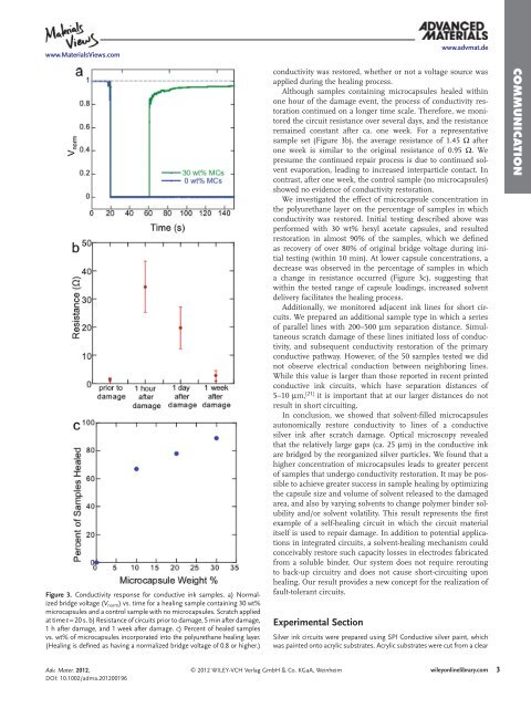
www.MaterialsViews.com Figure 3 . Conductivity response for conductive ink samples. a) Normalized bridge voltage ( V norm ) vs. time for a healing sample containing 30 wt% microcapsules and a control sample with no microcapsules. Scratch applied at time t = 20 s. b) Resistance of circuits prior to damage, 5 min after damage, 1 h after damage, and 1 week after damage. c) Percent of healed samples vs. wt% of microcapsules incorporated into the polyurethane healing layer. (<strong>Healing</strong> is defi ned as having a normalized bridge voltage of 0.8 or higher.) Adv. Mater. 2012, DOI: 10.1002/adma.201200196 © 2012 WILEY-VCH Verlag GmbH & Co. KGaA, Weinheim www.advmat.de conductivity was restored, whether or not a voltage source was applied during the healing process. Although samples containing microcapsules healed within one hour of the damage event, the process of conductivity restoration continued on a longer time scale. Therefore, we monitored the circuit resistance over several days, and the resistance remained constant after ca. one week. For a representative sample set ( Figure 3 b), the average resistance of 1.45 Ω after one week is similar to the original resistance of 0.95 Ω . We presume the continued repair process is due to continued solvent evaporation, leading to increased interparticle contact. In contrast, after one week, the control sample (no microcapsules) showed no evidence of conductivity restoration. We investigated the effect of microcapsule concentration in the polyurethane layer on the percentage of samples in which conductivity was restored. Initial testing described above was performed with 30 wt% hexyl acetate capsules, and resulted restoration in almost 90% of the samples, which we defi ned as recovery of over 80% of original bridge voltage during initial testing (within 10 min). At lower capsule concentrations, a decrease was observed in the percentage of samples in which a change in resistance occurred ( Figure 3 c), suggesting that within the tested range of capsule loadings, increased solvent delivery facilitates the healing process. Additionally, we monitored adjacent ink lines for short circuits. We prepared an additional sample type in which a series of parallel lines with 200–500 μ m separation distance. Simultaneous scratch damage of these lines initiated loss of conductivity, and subsequent conductivity restoration of the primary conductive pathway. However, of the 50 samples tested we did not observe electrical conduction between neighboring lines. While this value is larger than those reported in recent printed conductive ink circuits, which have separation distances of 5–10 μ m, [ 21 ] it is important that at our larger distances do not result in short circuiting. In conclusion, we showed that solvent-fi lled microcapsules autonomically restore conductivity to lines of a conductive silver ink after scratch damage. Optical microscopy revealed that the relatively large gaps (ca. 25 μ m) in the conductive ink are bridged by the reorganized silver particles. We found that a higher concentration of microcapsules leads to greater percent of samples that undergo conductivity restoration. It may be possible to achieve greater success in sample healing by optimizing the capsule size and volume of solvent released to the damaged area, and also by varying solvents to change polymer binder solubility and/or solvent volatility. This result represents the fi rst example of a self-healing circuit in which the circuit material itself is used to repair damage. In addition to potential applications in integrated circuits, a solvent-healing mechanism could conceivably restore such capacity losses in electrodes fabricated from a soluble binder. Our system does not require rerouting to back-up circuitry and does not cause short-circuiting upon healing. Our result provides a new concept for the realization of fault-tolerant circuits. Experimental Section Silver ink circuits were prepared using SPI <strong>Conductive</strong> silver paint, which was painted onto acrylic substrates. Acrylic substrates were cut from a clear wileyonlinelibrary.com 3 COMMUNICATION
COMMUNICATION 4 www.advmat.de cast acrylic sheet 0.15 cm thick, purchased from McMaster-Carr, catalog number 8560K175. Clear Flex 50, a two-part polyurethane elastomer, was purchased from Smooth On, Inc. Hexyl acetate, urea, resorcinol, and formalin were purchased from Aldrich Chemical Co. Ethylene-maleic anhydride copolymer (Zemac-400) powder with an average molecular weight of 400 kDa (Vertellus) was used as a 2.5 wt% aqueous solution. The commercial polyurethane prepolymer, Desmodur L75, was purchased from Bayer Material Science and was used as received. Microcapsule Preparation : Microcapsules were prepared with slight modifi cations using our previously published procedures . wileyonlinelibrary.com [ 29 , 30 ] Similarly, 100 mL of distilled water was placed in a 600 mL beaker, along with 25 mL of 2.5 wt% ethylene co-maleic anhydride as a surfactant. The beaker was placed in a temperature-controlled water bath equipped with a mechanical stirring blade (40 mm diameter), which was brought to 400 rpm. To the aqueous solution was added the solid wall-forming materials: urea (2.50 g), ammonium chloride (0.25 g), and resorcinol (0.25 g). Afterward, the pH was raised from 2.7 to 3.5 by addition of NaOH (aq). Desmodur L75 (4 g) in hexyl acetate (60 mL) was added to the stirring solution, creating an emulsion. After 10 min, 6.33 g of formalin solution was added, and the temperature was increased to 55 ºC. The reaction proceeded under continuous stirring for 4 h after which the reaction mixture was allowed to cool to room temperature. The microcapsules were fi ltered the next day using a Buchner funnel, washing with water, and were dried under air for 24 h before sieving. Microcapsule Analysis : After isolation via fi lteration, microcapsules were sieved to collect those with diameters ranging from 125–180 μ m. Optical micrographs of dried capsules in mineral oil on glass slides were taken using a Leica DMR Optical Microscope. Images of dried capsules were obtained using SEM (FEI/Philips XL30 ESEM-FEG) after sputter coating with a gold-palladium source. Thermogravimetric analysis (TGA) was performed on a Mettler-Toledo TGA851 e , calibrated by indium, aluminum, and zinc standards. A heating rate of 10 ºC min − 1 was used, and experiments were performed under nitrogen atmosphere from 25–450 ºC. For each experiment, approximately 5 mg of sample was used. Wheatstone Bridge Circuit : The conductive metal in each specimen acts as one resistor in an unbalanced constant voltage Wheatstone Bridge circuit. The voltage source is a BK Precision DC Power Supply (model 1710). The voltage gauge and voltage source are monitored by LabVIEW DAQ. Scratch damage was applied using a Corrocutter with razor blades at forces ranging from 28–30 N. A new razor blade was used for each measurement to ensure consistency in the integrity of the blade for each sample. Circuit Fabrication : Each circuit was 3 mm wide and ranged from 20–50 μ m in thickness, as measured by profi lometry. Each test sample contained three circuits to allow for testing of multiple samples at at the same time. Using a polydimethylsiloxane (PDMS) mold, a 1 mm thick fi lm of polyurethane elastomer containing 0, 10, 20, or 30 wt% microcapsules was deposited on top of the silver particle circuits. Wires were then attached to the circuits using copper pads and solder. Sample Imaging : To obtain cross-sectional images, a diamond saw was used to cut thin slices of the circuits; our cuts were made perpendicular to the direction in which the scratch was applied. The samples were analyzed by SEM with analysis in refl ectance mode. Not only are the conductive ink and capsule-containing polyurethane damaged, but the scratch also extends into the supporting polymer substrate. Supporting Information Supporting Information is available from the Wiley Online Library or from the author. Received: January 13, 2012 Published online: © 2012 WILEY-VCH Verlag GmbH & Co. KGaA, Weinheim www.MaterialsViews.com [ 1 ] Proceedings of EuroSIME, Paris (Eds: R. B. R. van Silfhout , Y. Li , W. D. van Driel , L. J. Ernst ) Shaker Publishing BV , Maastricht 2001. [ 2 ] P. Viswanadham , P. Singh , Failure Modes and Mechanisms in Electronic Packages , Chapman & Hall , London 1998 . [ 3 ] J. W. Hutchinson , Z. Suo , Adv. Appl. Mech. 1992 , 29 , 63 . [ 4 ] P. Servati , A. Nathan , Appl. Phys. Lett. 2005 , 86 , 033504 . [ 5 ] G. Crawford , Flexible Flat Panel Display Technology , John Wiley & Sons, Ltd. , Chichester, UK 2005 . [ 6 ] J. Vetter , P. Novák , M. R. Wagner , C. Velt , K.-C. Möller , J. O. Besenhard , M. Winter , M. Wohlfahrt-Mehrens , C. Vogler , A. Hammouche , J. Power Sources 2005 , 147 , 269 . [ 7 ] H. Gabrisch , J. Wilcox , M. M. Doeff , Electrochem. Solid-State Lett. 2008 , 11 , A25 . [ 8 ] J. Christensen , J. Newman , J. Electrochem. Soc. 2006 , 153 , A1019 . [ 9 ] Y. Itou , Y. Ukyo , J. Power Sources 2005 , 146 , 39 . [ 10 ] M. M. Caruso , S. R. Schelkopf , A. C. Jackson , A. M. Landry , P. V. <strong>Braun</strong> , J. S. Moore , J. Mater. Chem. 2009 , 19 , 6093 . [ 11 ] S. A. Odom , M. M. Caruso , A.D. Finke , A. M. Prokup , J. A. Ritchey , J. H. Leonard , S. R. White , N. R. Sottos , J. S. Moore , Adv. Funct. Mater. 2010 , 20 , 1721 . [ 12 ] B. J. Blaiszik , S. L. B. Kramer , M. E. Grady , D. A. McIlroy , J. S. Moore , N. R. Sottos , S. R. White , Adv. Mater. 2012 , 24 , 398 . [ 13 ] K. A. Williams , A. J. Boydston , C. W. Bielawski , J. R. Soc. Interface 2007 , 4 , 359 . [ 14 ] S. Gupta , Q. Zhang , T. Emrick , A. C. Balazs , T. P. Russell , Nat. Mater. 2006 , 5 , 229 . [ 15 ] G. V. Kolmakov , R. Revanur , R. Tangirala , T. Emrick , T. P. Russell , A. J. Crosby , A. C. Balazs , ACS Nano 2010 , 4 , 1115 . [ 16 ] A. Akoglu , A. Sreeramareddy , J. G. Josiah , Cluster Computing 2009 , 12 , 269 . [ 17 ] K. F. Teng , R. W. Vest , IEEE Trans. Comp. Hybrids and Manuf. Tech. 1987 , 10 , 545 . [ 18 ] R. K. F. Teng , A. A. Mostafa , A. Karim , IEEE Trans. Ind. Electron. 1990 , 37 , 419 . [ 19 ] M. H. Cheong , S. Wagner , IEEE Electron Dev. Lett. 2000 , 21 , 384 . [ 20 ] D. J. Hayes , W. R. Cox , M. E. Grove , J. Electron. Manuf. 1998 , 8 , 209 . [ 21 ] B. Y. Ahn , E. B. Duoss , M. J. Motala , X. Guo , S.-I. Park , Y. Xiong , J. Yoon , R. Nuzzo , J. A. Rogers , J. A. Lewis , Science 2009 , 323 , 1590 . [ 22 ] J. J. Adams , E. B. Duoss , T. F. Malkowski , M. J. Motala , B. Y. Ahn , R. G. Nuzzo , J. T. Bernhard , J. A. Lewis , Adv. Mater. 2011 , 23 , 1335 . [ 23 ] A. Russo , B. Y. Ahn , J. J. Adams , E. B. Duoss , J. T. Bernhard , J. A. Lewis , Adv. Mater. 2011 , 23 , 3426 . [ 24 ] M. Hosokawa , K. Nogi , M. Naito , T. Yokoyama , Nanoparticle Technology Handbook , Elsevier , Oxford 2007 . [ 25 ] P. R. Shepherd , P. S. A. Evans , B. J. Ramsey , D. J. Harrison , Electronics Lett. 1997 , 33 , 483 . [ 26 ] S.-C. Hung , O. A. Nafday , J. R. Haaheim , F. Ren , G. C. Chi , S. J. Pearton , J. Phys. Chem. C 2010 , 114 , 9672 . [ 27 ] J.-U. Park , S. Lee , S. Unarunotia , Y. Sun , S. Dunham , T. Song , P. M. Ferreira , A. G. Alleyene , U. Paik , J. A. Rogers , Nano Lett. 2010 , 10 , 584 . [ 28 ] B. Y. Ahn , D. J. Lorang , J. A. Lewis , Nanoscale 2011 , 3 , 2700 . [ 29 ] M. M. Caruso , B. J. Blaiszik , S. R. White , N.R. Sottos , J. S. Moore , Adv. Funct. Mater. 2008 , 18 , 1898 . [ 30 ] M. M. Caruso , B. J. Blaiszik , H. Jin , S. R. Schelkopf , D. S. Stradley , N. R. Sottos , S. R. White , J. S. Moore , ACS Appl. Mater. Interfaces 2010 , 2 , 1195 . Adv. Mater. 2012, DOI: 10.1002/adma.201200196