

Epitaxial growth and device fabrication of GaN based - Lehighton ...
Epitaxial growth and device fabrication of GaN based - Lehighton ...
Epitaxial growth and device fabrication of GaN based - Lehighton ...

You also want an ePaper? Increase the reach of your titles
YUMPU automatically turns print PDFs into web optimized ePapers that Google loves.
10th European Workshop on MOVPE, Lecce (Italy) 8−11 June 2003 INV.08<br />
<strong>Epitaxial</strong> <strong>growth</strong> <strong>and</strong> <strong>device</strong> <strong>fabrication</strong> <strong>of</strong> <strong>GaN</strong> <strong>based</strong> electronic <strong>and</strong> optoelectronic<br />
structures<br />
S. Müller 1) , R. Quay 1) , F. Sommer 1) , F. Vollrath 1) , R. Kiefer 1) , K. Köhler 1) , J. Wagner 1)<br />
1) Fraunh<strong>of</strong>er−Institut für Angew<strong>and</strong>te Festkörperphysik, Tullastrasse 72, 79108 Freiburg, Germany<br />
1.Introduction<br />
At the Fraunh<strong>of</strong>er IAF both single <strong>and</strong> multiwafer low−pressure MOVPE reactors are used for the <strong>growth</strong> <strong>of</strong> a)<br />
<strong>GaN</strong>/Al<strong>GaN</strong> layer sequences for the <strong>fabrication</strong> <strong>of</strong> high electron mobility transistors (HEMTs) <strong>and</strong> b) complex<br />
GaInN/<strong>GaN</strong>/Al<strong>GaN</strong> layer structures for violet <strong>and</strong> UV LEDs as well as violet emitting diode lasers. In the<br />
following both <strong>growth</strong> related issues as well as results on <strong>device</strong>s fabricated from these epitaxial layer sequences<br />
will be discussed in section 2 for electronic <strong>device</strong>s <strong>and</strong> in section 3 for light emitting diodes <strong>and</strong> diode lasers.<br />
2. Al<strong>GaN</strong>/<strong>GaN</strong> <strong>based</strong> HEMT<br />
High electron mobility transistors (HEMTs) <strong>based</strong> on <strong>GaN</strong>/Al<strong>GaN</strong> heterostructures are well suited for high power<br />
microwave amplifiers covering the 2 – 40 GHz frequency range [1−3]. The main advantages <strong>of</strong> <strong>GaN</strong> over Si <strong>and</strong><br />
GaAs stem from its wide b<strong>and</strong>gap, hence high breakdown field <strong>and</strong> high electron saturation velocity. This material<br />
<strong>of</strong>fers large potential to surpass existing <strong>device</strong> limitations in RF output power, operation voltage <strong>and</strong> operation<br />
temperature. The HEMT structures can be grown either on sapphire or on s.i. SiC substrates. Sapphire is available<br />
at significantly lower costs <strong>and</strong> in larger sizes than SiC <strong>and</strong> is successfully used for optoelectronic <strong>device</strong>s (see<br />
below). However, to develop full RF performance, the dissipated power has to be removed as effectively as<br />
possible. Therefore s.i. SiC is the substrate <strong>of</strong> choice providing an excellent thermal conductivity <strong>of</strong> 3.5 W/cm·K,<br />
which is an order <strong>of</strong> magnitude higher than that <strong>of</strong> sapphire.<br />
a) Epitaxy <strong>and</strong> characterization<br />
The HEMT structures are grown in an AIXTRON 2000 G3 HT 6´2" multiwafer reactor. On SiC a 500 nm thick<br />
Al<strong>GaN</strong> layer is grown followed by a 2.75 µm thick highly insulating <strong>GaN</strong> buffer layer. The spontaneous <strong>and</strong><br />
piezoelectric polarization <strong>of</strong> a 25 nm thick Al0.25 Ga0.75 N layer on top <strong>of</strong> the buffer results in a two−dimensional<br />
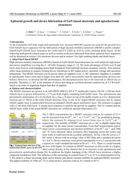
electron gas (2−DEG) at the <strong>GaN</strong>/Al<strong>GaN</strong> interface (Fig. 1) [4]. In Si−doped HEMT structures the Si−doped<br />
Al<strong>GaN</strong> supply layer is s<strong>and</strong>wiched between an undoped Al<strong>GaN</strong> spacer <strong>and</strong> barrier layer. The structure is capped<br />
with a 2 nm thick <strong>GaN</strong> layer. A similar layer sequence is used for the <strong>growth</strong> on sapphire. The Al−content <strong>and</strong> the<br />
Al<strong>GaN</strong> layer width <strong>of</strong> the actual HEMT structures are verified by spectral ellipsometry [5].<br />
The 2−DEG concentration for a HEMT−structure with an Al−content <strong>of</strong> 25 %<br />
can be increased from 4x10 12 cm −2 to 1.5x10 13 cm −2 by modulation doping,<br />
where the nominal Si−doping level varies from zero to 3x10 19 cm −3 ,<br />
respectively. The mobility <strong>of</strong> HEMT−structures on s.i. SiC is slightly higher than<br />
on sapphire for the same carrier concentration. From Hall measurements typical<br />
sheet carrier concentrations <strong>and</strong> electron mobilities <strong>of</strong> 8x10 12 cm −2 <strong>and</strong> 1400<br />
cm 2 /Vs were obtained. Sheet resistance (Rs) mappings across the wafers <strong>and</strong><br />
from wafer to wafer proved an excellent uniformity. In Fig. 2 the Rs across a 2"<br />
SiC wafer is shown with an average value <strong>of</strong> 483 Ohm <strong>and</strong> a st<strong>and</strong>ard deviation<br />
<strong>of</strong> ± 0.6 %. Device structures were grown reproducibly over a 2 year period with<br />
a typical on−wafer st<strong>and</strong>ard deviation in Rs <strong>of</strong> 1 − 4 %. There is a trend towards<br />
<strong>device</strong>s with higher Al content in HEMT structures as this results in a higher<br />
sheet carrier density in the channel due to an increase in the spontaneous <strong>and</strong><br />
piezoelectric polarization charge [4]. In addition the higher b<strong>and</strong>gap <strong>of</strong> the Al<strong>GaN</strong> layer promises a higher<br />
composite breakdown field. The influence <strong>of</strong> the increasing Al content from 25 % to 35 % is demonstrated in Fig.<br />
3. We observe a linear increasing sheet carrier density <strong>and</strong> almost constant mobility for undoped HEMT structures.<br />
The highest mobility <strong>of</strong> 1500 cm 2 /Vs is achieved for a structure with an Al−content <strong>of</strong> 30 %.<br />
Mueller Stefan
10th European Workshop on MOVPE, Lecce (Italy) 8−11 June 2003 INV.08<br />
b) Process technology <strong>and</strong> <strong>device</strong> performance<br />
Device <strong>fabrication</strong> was done on full 2" wafers by contact lithography. Device isolation<br />
was accomplished by a 180 nm deep mesa dry etch into the <strong>GaN</strong> buffer by chemically<br />
assisted ion beam etching using chlorine.<br />
Ti/Al/Au alloyed ohmic contacts were used, obtaining an average contact resistance <strong>of</strong><br />
0.6 Ohm*mm. The T−shaped Ni/Au−gates were defined by electron−beam lithography<br />
with a minimum gatelength <strong>of</strong> 0.15 µm. A scanning electron microscope image <strong>of</strong> the<br />
T−gate in the source drain area is shown in Fig. 4. All <strong>device</strong>s were passivated by a 100<br />
nm thick SiN layer <strong>and</strong> multi−finger transistors were fabricated using first level metal<br />
interconnects <strong>and</strong> galvanic Au air bridges. The quality <strong>of</strong> the grown epitaxial layers <strong>and</strong><br />
the subsequent processing technology is confirmed by CW load pull measurements at 2<br />
GHz <strong>and</strong> 40 GHz (Fig. 5 <strong>and</strong> 6, respectively). Results from a <strong>device</strong> with 2 mm<br />
gatewidth <strong>and</strong> a gatelength <strong>of</strong> 300 nm are shown in Fig. 5. A linear gain <strong>of</strong> 23 dB, a<br />
maximum output power <strong>of</strong> 11.6 W yielding 5.8 W/mm, <strong>and</strong> a power added efficiency<br />
beyond 55 % are obtained under CW operating conditions. For a 150 nm <strong>GaN</strong>/Al<strong>GaN</strong><br />
HEMT with a gatewidth <strong>of</strong> 8*60 µm, a linear gain beyond 5.5 dB, a maximum output<br />
power <strong>of</strong> 0.86 W yielding 1.8 W/mm, <strong>and</strong> a maximum PAE beyond 10 % are achieved<br />
(Fig. 6). The value <strong>of</strong> 0.86 W (1.8 W/mm) obtained for a single <strong>device</strong> at 40 GHz is, to<br />
our knowledge so far, the highest CW output power achieved with Al<strong>GaN</strong>/<strong>GaN</strong> <strong>based</strong><br />
HEMT technology. Even at 40 GHz, an advantage <strong>of</strong> at least a factor <strong>of</strong> 3 in power<br />
density is gained with <strong>GaN</strong> technology in comparison to the mature GaAs PHEMT<br />
process [6].<br />
3. LED <strong>and</strong> laser <strong>device</strong>s<br />
Blue light emitting diodes (LEDs) were the first <strong>device</strong>s to be realized from group<br />
III−nitride compound semiconductors, after Amano et al. solved the problem <strong>of</strong> viable<br />
p−type doping [7]. In the last couple years <strong>GaN</strong> <strong>based</strong> LEDs covering the spectral<br />
window from green to near UV, are extending their range <strong>of</strong> application, including<br />
traffic signals, display <strong>and</strong> automotive application, environmental protection or even<br />
general lightning. The key advantages <strong>of</strong> these solid state light sources are lower energy<br />
consumption, long <strong>device</strong> lifetime <strong>and</strong> mechanical robustness. In lightning applications<br />
white LEDs are expected to outperform both inc<strong>and</strong>escent <strong>and</strong> fluorescent light sources<br />
within the next decade. While single chip white LEDs − using a blue LED chip <strong>and</strong> a<br />
yellow phosphor converter − are already commercially available, white LEDs using a<br />
violet or UV pump LED <strong>and</strong> a tri−phosphor blend, which are expected to have an<br />
improved color rendering, are currently still under development. A prerequisite for use<br />
<strong>of</strong> these LEDs in general lightning application, however, is a further increase in the<br />
efficiency <strong>of</strong> the LED chips.<br />
Since the first demonstration <strong>of</strong> a III−N <strong>based</strong> blue laser diode (LD) by Nakamura et al.<br />
in 1996 [8], several other groups including Sony, Xerox or Osram have announced the<br />
successful <strong>fabrication</strong> <strong>of</strong> blue/violet laser <strong>device</strong>s [9−11]. Such short wavelength<br />
semiconductor diode lasers will find a variety <strong>of</strong> applications including high density<br />
optical data storage (DVD−RAM / Blue Ray Disk), laser printing, spectroscopy, sensing<br />
<strong>and</strong> projection displays. Ultra high density optical data storage in DVD systems with a<br />
capacity exceeding 10 gigabytes is one <strong>of</strong> the key applications <strong>of</strong> violet light emitting<br />
diode lasers. Unfortunately many <strong>of</strong> these lasers still suffer from short lifetime due to<br />
the high density <strong>of</strong> dislocation in the layers structure resulting from the large lattice<br />
mismatch between <strong>GaN</strong> <strong>and</strong> the substrate. The reliability can be significantly improved<br />
by using epitaxially lateral overgrown (ELOG) <strong>GaN</strong> [12, 13] on sapphire or even the<br />
epitaxial <strong>growth</strong> <strong>of</strong> the laser structure on freest<strong>and</strong>ing <strong>GaN</strong> substrates. Nagahama<br />
(Nichia) demonstrated laser <strong>device</strong>s with an estimated lifetime <strong>of</strong> 15000 hours under 30<br />
mW CW operation at 60 °C [14].<br />
a) Epitaxy <strong>of</strong> (AlInGa)N <strong>based</strong> LEDs for the <strong>fabrication</strong> <strong>of</strong> white LEDs<br />
Layer sequences for violet <strong>and</strong> near UV emitting (AlInGa)N <strong>based</strong> LEDs were grown by low pressure MOVPE,<br />
both in our single <strong>and</strong> multiwafer reactor on conventional (unpatterned) 2” sapphire substrates. The layer structure<br />
presented in Fig. 7 consists <strong>of</strong> <strong>of</strong> 25 nm LT <strong>GaN</strong> nucleation layer, a 2000 nm undoped <strong>GaN</strong> buffer, a 1500 nm<br />
Si−doped ([Si]=1E19 cm −3 ) n−contact layer, the active layer with an In<strong>GaN</strong>/<strong>GaN</strong> single or multiple quantum<br />
wells followed by a thin Al<strong>GaN</strong>:Mg electron blocking layer <strong>and</strong> the 200 nm thick Mg−doped ([Mg]=0.7..1.5E20<br />
cm −3 ) p−<strong>GaN</strong> contact layer. After the epitaxial <strong>growth</strong> the wafers were characterized by on wafer<br />
Mueller Stefan
10th European Workshop on MOVPE, Lecce (Italy) 8−11 June 2003 INV.08<br />
elelectroluminescence (EL) measurements. Indium contacts are used to connect the p− <strong>and</strong> n−type <strong>GaN</strong> layers for<br />
rapid testing. Fig. 8 shows the EL output power <strong>of</strong> such an LED as a function <strong>of</strong> drive current, exceeding 3 mW @<br />
20 mA with a peak wavelength <strong>of</strong> l = 395 nm.<br />
In order to realize luminescence converting (LUCO) LEDs, the<br />
above described <strong>and</strong> characterized epitaxial layer sequences were<br />
processed into mesa LEDs by st<strong>and</strong>ard optical lithography <strong>and</strong><br />
chemically assisted ion beam etching (CAIBE). Electrical contacts<br />
to the n− <strong>and</strong> p−<strong>GaN</strong> contact layers were fabricated by lift−<strong>of</strong>f<br />
technique, using Ti/Al/Ni/Au <strong>and</strong> Ni/Au as the n− <strong>and</strong> p−contact<br />
metalizations, respectively.<br />
Several alternative approaches exist towards the realization <strong>of</strong> white<br />
emitting single−chip LEDs <strong>based</strong> on the principle <strong>of</strong> luminescence<br />
conversion. The so far most widely used approach combines a blue<br />
emitting (AlGaIn)N <strong>based</strong> LED chip with a yellow emitting<br />
YAG:Ce phosphor, yielding white light by additive color mixing<br />
when the relative intensities <strong>of</strong> the blue <strong>and</strong> yellow light component<br />
are adjusted appropriately. This approach has certain advantages<br />
because <strong>of</strong> its simplicity <strong>and</strong> its good overall power efficiency, as<br />
only one <strong>of</strong> the two primary colors is generated by luminescence<br />
conversion, thus limiting conversion losses due to Stokes shift. On<br />
the other h<strong>and</strong> the range <strong>of</strong> color coordinates, which can be covered<br />
by this approach, as well as the color rendering achieved, are<br />
limited.<br />
To overcome these shortcomings, a violet/UV emitting LED chip is<br />
used as pump light source, whose short wavelength emission is not<br />
to be perceived by the human eye. The LED chip then excites a<br />
blend <strong>of</strong> three phosphors, converting the pump light into blue, green<br />
<strong>and</strong> red light (RGB−conversion), respectively [15]. This way, for a<br />
homogenous tri−color phosphor blend, a change in optical path<br />
length affects only the total amount <strong>of</strong> light converted, <strong>and</strong> thus the<br />
overall light intensity, <strong>and</strong> not the color coordinates as is the case<br />
for the more simple blue/yellow mixing LED. On the other h<strong>and</strong><br />
this approach is particularly dem<strong>and</strong>ing with respect to the required<br />
optical properties <strong>of</strong> the phosphors employed. Using near−UV<br />
emission in the 390 to 400 nm wavelength range to reduce losses in<br />
overall conversion efficiency by minimizing the quantum deficit,<br />
requires a blue emitting phosphor with a particularly small Stokes<br />
shift between absorption <strong>and</strong> emission, while maintaining a high<br />
conversion efficiency, <strong>and</strong> a red−emitting compound with a<br />
particularly large Stokes shift for direct pumping by the LED rather<br />
than by the emission <strong>of</strong> the blue phosphor. While ensuring the best<br />
quality <strong>of</strong> white light emission in terms <strong>of</strong> color tuning, color<br />
rendering, <strong>and</strong> independence <strong>of</strong> color impression on viewing angle,<br />
a certain price will have to be paid in terms <strong>of</strong> overall power<br />
efficiency as all three color components <strong>of</strong> the white light are<br />
generated by luminescence conversion. Such UV pumped single−chip white LEDs with RGB tri−color<br />
luminescence conversion have been realized at the IAF in close collaboration with Osram Opto Semiconductors,<br />
Osram GmbH, <strong>and</strong> Siemens AG as industrial partners. Rare earth doped oxide <strong>and</strong> sulfide materials have been<br />
identified as appropriate inorganic RGB phosphors for optical pumping at wavelengths just below<br />
Mueller Stefan
10th European Workshop on MOVPE, Lecce (Italy) 8−11 June 2003 INV.08<br />
the short−wavelength cut−<strong>of</strong>f <strong>of</strong> the sensitivity <strong>of</strong> the human eye. Powders <strong>of</strong> these phosphors were dispersed in<br />
epoxy resin <strong>and</strong> detailed tests were carried out to determine the<br />
optimum phosphor concentrations with respect to conversion<br />
efficiency as well as with respect to the targeted color coordinates.<br />
Fig. 9 shows the EL spectrum <strong>of</strong> an UV−pumped tri−phosphor white<br />
LED employing a LED chip emitting at 394 nm. Chip <strong>and</strong> converter<br />
were encapsulated in epoxy using a st<strong>and</strong>ard 5 mm radial LED<br />
package. Besides residual emission from the pump chip, three<br />
phosphor−related emission b<strong>and</strong>s centered at 460 nm, 550 nm, <strong>and</strong><br />
610 nm are resolved. The CIE color coordinates are x=0.365 <strong>and</strong><br />
y=0.359 at an injection current <strong>of</strong> 20 mA, resulting in a color<br />
temperature <strong>of</strong> 4300 K. These parameters are those <strong>of</strong> a warm white<br />
hue, which cannot be generated by single−phosphor blue/yellow<br />
LEDs. Further optimization <strong>of</strong> the individual phosphors <strong>and</strong> <strong>of</strong> the<br />
phosphor blend will be required to improve the overall conversion<br />
efficiency.<br />
b) Blue laser diodes<br />
The approach adopted by the Fraunh<strong>of</strong>er IAF for the <strong>fabrication</strong> <strong>of</strong><br />
short wavelength diode lasers is <strong>based</strong> on the MOVPE <strong>growth</strong> <strong>of</strong><br />
appropriate (AlGaIn)N layer sequences on 2” sapphire substrates.<br />
Based on our blue/violet LED structure, the layer sequence has been<br />
modified appropriately for the realization <strong>of</strong> the laser structure. The<br />
active region is composed <strong>of</strong> GaInN/<strong>GaN</strong> single or multiple QWs with<br />
an Al<strong>GaN</strong> electron barrier towards the p−contact, embedded between<br />
n− <strong>and</strong> p−doped <strong>GaN</strong> separate confinement layers <strong>and</strong> n− <strong>and</strong><br />
p−doped Al<strong>GaN</strong> cladding layers. Using c−plane sapphire substrate<br />
rules out the use <strong>of</strong> conventional cleaving to form the laser mirrors.<br />
Thus mirrors are prepared by chemically assisted ion beam etching<br />
(CAIBE) in conjunction with a resist mask defined by<br />
photolithography. A schematic view <strong>of</strong> an (AlGaIn)N <strong>based</strong> ridge<br />
waveguide diode laser on insulating sapphire substrate is shown in<br />
Fig. 10, featuring etched mirror facets <strong>and</strong> a mesa etch for n−contact<br />
formation. A typical epitaxial structure for short wavelength diode<br />
lasers realized on sapphire substrates is shown in Fig. 11.<br />
Pulsed output power vs. current characteristics <strong>of</strong> a series <strong>of</strong> 4x500<br />
µm 2 ridge waveguide laser <strong>device</strong>s on sapphire fabricated from<br />
different epitaxial series are shown in Fig. 12. There is a clear<br />
reduction in threshold current with increasing sample number from (a)<br />
to (e), reflecting the progress achieved in epitaxial layer design <strong>and</strong><br />
MOVPE <strong>growth</strong>. The lowest threshold current density measured for a<br />
4x500 µm 2 <strong>device</strong> is 13.9 kA/cm 2 , which corresponds to a threshold<br />
current <strong>of</strong> 279 mA. An extrapolation <strong>of</strong> the best values <strong>of</strong> Ith towards<br />
infinite cavity length yields Ith,oo = 6.3 kA/cm 2 . The slope efficiency<br />
amounts h = 415 mW/A per facet <strong>and</strong> the wavelength <strong>of</strong> the emitted<br />
laser light is l = 411 nm. The characteristic temperature T0 <strong>and</strong> T1,<br />
describing the temperature dependence <strong>of</strong> the threshold current <strong>and</strong> the<br />
slope efficiency, respectively, are 165 K <strong>and</strong> 210 K. All these data apply to <strong>device</strong>s without reflective facet coating<br />
<strong>and</strong> have been measured on wafer in pulse mode (200 ns pulse width, 0.2 % duty cycle) at 15 °C. Future work will<br />
focus on further lowering <strong>of</strong> threshold current <strong>and</strong> operating voltage as well as on a reduction <strong>of</strong> the defect density<br />
Mueller Stefan
10th European Workshop on MOVPE, Lecce (Italy) 8−11 June 2003 INV.08<br />
by using appropriate <strong>GaN</strong> substrates, a necessity for long lived diode lasers.<br />
Conclusions<br />
We have demonstrated the <strong>growth</strong> <strong>of</strong> <strong>GaN</strong>/Al<strong>GaN</strong> heterostructures by MOVPE for power HEMT applications. The<br />
electrical properties <strong>of</strong> the 2−DEG as well as the excellent uniformity <strong>of</strong> the wafers are ideal prerequisites for<br />
reproducible high yields for <strong>device</strong> <strong>fabrication</strong>. The quality <strong>of</strong> both epitaxy <strong>and</strong> processing is confirmed by CW<br />
load pull measurements at 2 GHz <strong>and</strong> 40 GHz with output power <strong>of</strong> 11.6 W <strong>and</strong> 0.86 W, respectively. Near UV<br />
emitting (AlInGa)N <strong>based</strong> LEDs covering the 380 to 430 nm wavelength range have been developed as pump<br />
sources for the <strong>fabrication</strong> <strong>of</strong> white LEDs. The optical output power <strong>of</strong> the near UV LED was up to 3 mW @ 20<br />
mA at l = 395 nm. Tricolor LUCO white LEDs have been produced <strong>and</strong> characterized <strong>and</strong> show superior color<br />
quality to that <strong>of</strong> YAG:Ce <strong>based</strong> white LEDs. Short wavelength diode laser structures have been grown on<br />
conventional 2” sapphire. Devices with uncoated mirror facets show lasing at l = 411 nm with a minimum<br />
threshold current <strong>of</strong> 278 mA, which corresponds to a threshold current density <strong>of</strong> 13.9 kA/cm −2 for the 500 µm*4<br />
µm <strong>device</strong>.<br />
Acknowledgement<br />
The authors acknowledge support <strong>of</strong> the German Federal Ministry <strong>of</strong> Education <strong>and</strong> Research (BMBF) <strong>and</strong> <strong>of</strong> the<br />
Federal Ministry <strong>of</strong> Defence (BMVg).<br />
References<br />
[1] Y.−F. Wu, B. P. Keller, S. Keller, P. Kapolnek, P. Kozodoy, S. P. DenBaars, <strong>and</strong> U. K. Mishra, Solid State<br />
Electron. 41, 1569−1574 (1997)<br />
[2] M. S. Shur, Solid State Electron. 42, 2131−2138 (1998)<br />
[3] H. Morkoc, A. Di Carlo, <strong>and</strong> R. Cingolati, Solid State Electron. 46, 157−202 (2002)<br />
[4] O. Ambacher, J. Smart, J. R. Shealy, N. G. Weimann, K. Chu, M. Murphy, R. Dimitrov, L. Wittmer, M.<br />
Stutzmann, W. Rieger, <strong>and</strong> J. Hilsenbeck, J. Appl. Phys. 85 3222−3233 (1999)<br />
[5] J. Wagner, H. Obloh, M. Kunzer, M. Maier, K. Köhler, <strong>and</strong> B. Johs, J. Appl. Phys. 89, No. 5 2779 (2001)<br />
[6] R. Quay, R. Kiefer, F. van Raay, H. Massler, S. Ramberger, S. Müller, M. Dammann, M. Mikulla, M.<br />
Schlechtweg, <strong>and</strong> G. Weimann, Int. Electron Dev. Meeting, San Francisco, session 28, (2002).<br />
[7] H. Amano, I. Akasaki, T. Kozawa, K. Hiramatsu, N. Sawak, K. Ikeda, <strong>and</strong> Y. Ishi, J. Lumin. 40−41, (1988)<br />
[8] S. Nakamura, M. Senoh, S. Nagahama, N. Iwasa, T. Yamada, T. Matsuhitah. Kiyoku, <strong>and</strong> Y. Sugimoto, Jpn.<br />
Mueller Stefan
10th European Workshop on MOVPE, Lecce (Italy) 8−11 June 2003 INV.08<br />
Appl. Phys. 35, L74 (1996)<br />
[9] M. Ikeda <strong>and</strong> S Uchida, phys. stat. sol. (a) 194, No.2, 407−413 (2002)<br />
[10] W. S. Wong, M. Kneissl, P. Mei, D. W. Treat, M. Teepe, <strong>and</strong> N. M. Johnson, Appl. Phys. Lett. 78, 1198<br />
(2001)<br />
[11] V. Kümmler, G. Brüderl, S. Bader, S. Miller, A. Weimar, A. Lell, V. Härle, U.T. Schwarz, N. Gmeinwieser,<br />
<strong>and</strong> W. Wegschneider, phys. stat. sol. (a) 194, No.2, 419−422 (2002)<br />
[12] A. Usui, H. Sunakawa, A. Sakai, <strong>and</strong> A. Yamaguchi, Jpn. J. Appl. Phys. 36 L899−L902 (1997)<br />
[13] O.H. Nam, M.D. Bremser, T. Zheleva, <strong>and</strong> R.F. Davis Appl. Phys. Lett. 71, 2638 (1997)<br />
[14] S. Nagahama, N. Iwasa, M. Senoh, T. Matsushita, Y. Sugimoto, H. Kiyoku, T. Kozaki, M. Sano, H.<br />
Matsushita, H. Umemoto, K. Chocho, <strong>and</strong> T. Mukai, Jpn. J. Appl. Phys. 39, L647−L650 (2000)<br />
[15] U. Kaufmann, M. Kunzer, K. Köhler, H. Obloh, W. Pletschen, P. Schlotter, R. Schmidt, J. Wagner, A. Ellens,<br />
<strong>and</strong> M. Kobusch, phys. stat. sol. (a) 188, 143 (2001)<br />
Mueller Stefan