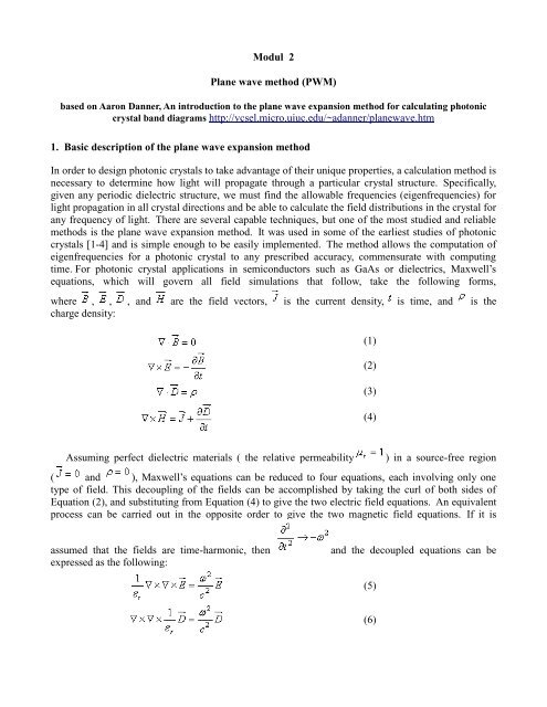
Modul 2 Plane wave method (PWM) crystal band diagrams http ...
Modul 2 Plane wave method (PWM) crystal band diagrams http ...
Modul 2 Plane wave method (PWM) crystal band diagrams http ...

Create successful ePaper yourself
Turn your PDF publications into a flip-book with our unique Google optimized e-Paper software.
<strong>Modul</strong> 2<br />
<strong>Plane</strong> <strong>wave</strong> <strong>method</strong> (<strong>PWM</strong>)<br />
based on Aaron Danner, An introduction to the plane <strong>wave</strong> expansion <strong>method</strong> for calculating photonic<br />
<strong>crystal</strong> <strong>band</strong> <strong>diagrams</strong> <strong>http</strong>://vcsel.micro.uiuc.edu/~adanner/plane<strong>wave</strong>.htm<br />
1. Basic description of the plane <strong>wave</strong> expansion <strong>method</strong><br />
In order to design photonic <strong>crystal</strong>s to take advantage of their unique properties, a calculation <strong>method</strong> is<br />
necessary to determine how light will propagate through a particular <strong>crystal</strong> structure. Specifically,<br />
given any periodic dielectric structure, we must find the allowable frequencies (eigenfrequencies) for<br />
light propagation in all <strong>crystal</strong> directions and be able to calculate the field distributions in the <strong>crystal</strong> for<br />
any frequency of light. There are several capable techniques, but one of the most studied and reliable<br />
<strong>method</strong>s is the plane <strong>wave</strong> expansion <strong>method</strong>. It was used in some of the earliest studies of photonic<br />
<strong>crystal</strong>s [1-4] and is simple enough to be easily implemented. The <strong>method</strong> allows the computation of<br />
eigenfrequencies for a photonic <strong>crystal</strong> to any prescribed accuracy, commensurate with computing<br />
time. For photonic <strong>crystal</strong> applications in semiconductors such as GaAs or dielectrics, Maxwell’s<br />
equations, which will govern all field simulations that follow, take the following forms,<br />
where , , , and are the field vectors, is the current density, is time, and is the<br />
charge density:<br />
Assuming perfect dielectric materials ( the relative permeability ) in a source-free region<br />
( and ), Maxwell’s equations can be reduced to four equations, each involving only one<br />
type of field. This decoupling of the fields can be accomplished by taking the curl of both sides of<br />
Equation (2), and substituting from Equation (4) to give the two electric field equations. An equivalent<br />
process can be carried out in the opposite order to give the two magnetic field equations. If it is<br />
assumed that the fields are time-harmonic, then and the decoupled equations can be<br />
expressed as the following:<br />
(1)<br />
(2)<br />
(3)<br />
(4)<br />
(5)<br />
(6)
Note that the forms for and are identical. This is expected because is constant in the<br />
equations. However, the relative permittivity is not constant in our structures (it is periodic), so the<br />
placement of the term is strict. The goal here is to find the energies and electromagnetic field<br />
configurations that are allowed to exist in a periodic structure. Essentially, what we are given in the<br />
problem is the , which will be a function of location, and we need to solve for and the fields.<br />
There are essentially three different choices of procedure at this point. All four equations, given a<br />
dielectric function, will yield one set of field distributions. (The and expansions give identical<br />
results.) After that, the other fields can simply be deduced from Maxwell’s equations. The question of<br />
which equation to solve depends on several factors. First, the equations for the magnetic fields<br />
(Equations (7) and (8)) are in a Hermitian form. Strictly speaking, the operator is<br />
Hermitian (see [5] for a detailed description of this property). Hermicity establishes that the<br />
eigenvalues are real, and that field distributions with the same eigenfrequency must be<br />
orthogonal. Usually, Hermitian eigenvalue problems are less complex computationally to solve [6], but<br />
the other forms should not be immediately overlooked as will be clear in the development which<br />
follows.<br />
Each of the decoupled equations above will yield three component equations if the vector<br />
operations are carried out. In Cartesian coordinates, they can be expressed as follows for the , ,<br />
and expansions, respectively. Expansions for are not simplified because in their full forms the<br />
extra terms generated by the inner make the expressions very long. (As seen in Equations (9) -<br />
(11), each equation of consists of four terms on the left side; each equation of or consists of<br />
eight terms; and each equation of would consist of sixteen terms. The chain rule applied repeatedly<br />
to the inner products creates the extra terms.)<br />
(7)<br />
(8)<br />
(9)
The fields themselves and the dielectric function can be expanded in Fourier series along the<br />
directions in which they are periodic. This Fourier expansion will be truncated to a fixed number of<br />
terms, limiting the accuracy of the calculation. The truncated problem will yield an eigenvalue<br />
equation for the fields which will allow calculation of the dispersion curves. It must be pointed out that<br />
regardless of which of the four decoupled equations is solved, the eigenvalues will be the same. For a<br />
fixed number of terms, the accuracy can be improved by a proper choice. For example, when solving a<br />
problem of air spheres embedded in a dielectric, using the expansion would yield much better<br />
convergence than the others, while using the or expansions would yield better results for<br />
dielectric spheres in air [6]. The analogy with the two-dimensional structures discussed here suggests<br />
that air cylinders drilled in a dielectric background may be a problem better suited for calculation using<br />
the expansion, in terms of matrix size. The accuracy differences among the three expansions result<br />
from the different resultant spatial orientations and positions of each field.<br />
The basic approach for calculating the field distribution and eigenfrequency given a dielectric<br />
function and propagation vector is to first expand and the three components of the appropriate field<br />
vector in Fourier series. These series are then substituted into the decoupled Maxwell’s equations and<br />
the terms are reorganized into an ordinary eigenvalue problem. When the eigenvalues are calculated<br />
(10)<br />
(11)
employing standard numerical <strong>method</strong>s (using a finite-sized matrix formed when the Fourier<br />
expansions are truncated), it is straightforward to use the eigenvalues to find the allowed propagation<br />
frequencies, and the eigenvectors to calculate the field distributions. The process is best illustrated by a<br />
simple example.<br />
2. Example: One-dimensional photonic <strong>crystal</strong><br />
The simplest example of a photonic <strong>crystal</strong> is a one-dimensional array of air slabs penetrating a<br />
dielectric background. Figure 1 shows the relevant axes. In this case, we will consider only <strong>wave</strong>s<br />
propagating in the +z direction. In most photonic <strong>crystal</strong> dispersion curves, it is usually difficult to<br />
distinguish curves as “transverse magnetic" (TM-like) or “transverse electric" (TE-like), but in this<br />
simple case there are two basic polarizations, viz., and . Here we consider the . case only,<br />
and begin the problem by assuming that the only field components present are , , and . Although the<br />
justification for this may not be immediately apparent, the symmetry in the problem permits<br />
this. There is also nothing wrong with using all components of and ; the mode separation is then<br />
easily seen. (Indeed, this is the <strong>method</strong> used in higher-dimensional photonic <strong>crystal</strong> problems.) Here,<br />
the purpose of the early simplification is to more clearly illustrate the <strong>method</strong>.<br />
Figure 1: One-dimensional photonic <strong>crystal</strong> consisting of air slabs of width d embedded in a dielectric<br />
background with a periodicity of a.<br />
With only one component, only a single line in Equation (9) remains, which demonstrates the<br />
justification for using the expansion:<br />
Now, Fourier series expansions for the field and dielectric can be applied. In this case, a Fourier<br />
expansion for the inverse dielectric function is used. Equivalently, the constant can be moved to<br />
the right side of the equation and could be expanded. This would form a generalized Hermitian<br />
eigenvalue problem, or an ordinary eigenvalue problem if an additional matrix inversion were carried<br />
out in the subsequent step. In the notation that follows, will represent all Fourier coefficients. The<br />
indices m and n are integers. The variable means “Fourier coefficients, indexed by the integer n, for the<br />
y-component of the electric field” and the variable means “Fourier coefficients, indexed by the integer m,<br />
(12)
for .” Ideally, the summations should be infinite, but will be truncated for computation purposes.<br />
Note that if propagation in a direction other than z had been included in the formulation, then the<br />
additional terms would have been included in Equation (14).<br />
After the Fourier expansions are substituted into Equation (12), the initial eigenvalue equation is<br />
obtained.<br />
To simplify, each side of this equation is multiplied by an orthogonal function , where p is an<br />
integer, and integrated over a unit cell, i.e., . For a nontrivial solution, p can take only one<br />
value so one summation on each side of the equation can be dropped. After reorganizing terms and<br />
renaming the sums to use only the letters m and n, the eigenequation takes its final form of<br />
This forms an ordinary eigenvalue problem, where the integers m and n are truncated symmetrically<br />
about zero as is appropriate for this type of Fourier expansion. This corresponds to including only<br />
lower order plane <strong>wave</strong>s in two dimensions. For example, if m and n were truncated to five terms (-2, -<br />
1, 0, 1, 2), then the full eigenvalue problem would appear as follows, using the<br />
notation :<br />
(13)<br />
(14)<br />
(16)<br />
(17)<br />
(15)
The matrix Q can be diagonalized using a variety of software packages and numerical <strong>method</strong>s, and the<br />
details will not be discussed here. After diagonalization, the eigenvalues and<br />
eigenvectors will be known. The eigenvalues give the dispersion diagram and the eigenvectors<br />
can be substituted back into the Fourier expansion for to find the field distribution at any given<br />
frequency.<br />
The only remaining problem is to find the dielectric coefficients , which can be obtained using<br />
the inverse Fourier transform:<br />
If the integral is split properly, then will be constant in the integration range. Depending upon<br />
where z = 0 is defined, the form of the result may take slightly different forms (but will make no<br />
difference as long as it is defined consistently):<br />
This is equivalent to the following, where the function :<br />
All information is now available to solve the Q matrix for the eigenvalues. Figure 2 shows the results<br />
for nine plane <strong>wave</strong>s (n and m are integers between -4 and 4 inclusive). In this case, a structure was<br />
chosen with a unit period, , and . Several <strong>band</strong>gaps are clearly visible for<br />
propagation in this direction. In this example we have examined only the case for propagation in<br />
the z direction. The interested reader is referred to [7] for a discussion of the case and off-axis<br />
propagation in the one-dimensional structure.<br />
In studies of photonic <strong>crystal</strong>s, the interest is usually not in the electric or magnetic field forms<br />
themselves. It is the eigenvalues that carry information on the location of the modes in<br />
momentum space. In the general case, varying values of , , and allows construction of a complete <strong>band</strong><br />
diagram. In more complicated structures, the <strong>band</strong> diagram is usually constructed at the boundaries of<br />
the Brillouin zone.<br />
(18)<br />
(20)<br />
(19)
Figure 2: Dispersion curve for propagation in the z direction for the one-dimensional photonic<br />
<strong>crystal</strong> structure. Note the presence of several <strong>band</strong>gaps.<br />
3. Fully vectorial, three-dimensional structures<br />
Essentially, the <strong>method</strong> remains the same for more complicated structures. Because of our interest in<br />
two-dimensional structures, we examine here the case of the triangular lattice of air holes embedded in<br />
a dielectric background. Using fabrication techniques described in the next chapter, arrays of holes can<br />
be created using electron beam lithography and etching <strong>method</strong>s. The result is a two-dimensional array<br />
of air holes in a semiconductor substrate. Therefore, for our interests the dielectric function will be<br />
periodic only in the xy plane (uniform in the z direction). This results in some simplification for<br />
the expansion. Although the structure studied is two-dimensional, propagation in all directions<br />
(including the out-of-plane propagation case) will be considered. Extension of this <strong>method</strong> to threedimensional<br />
structures is straightforward and will be explained. In the equations used, a is the lattice<br />
spacing of a unit cell; the lattice itself is triangular within a medium with dielectric<br />
constant perforated by infinite air holes (atoms) of diameter d. The 2D triangular lattice unit cell has<br />
been widely covered in literature [2, 3,5,8] and the <strong>method</strong> described here has been tested and gives<br />
equivalent results for the same problems. In this thesis, the triangular lattice supercell is further<br />
generalized to the Nx N case and <strong>method</strong> accuracy is treated. First, we discuss the unit cell.<br />
The general formulas for the Fourier expansions in the three-dimensional case, assuming use of<br />
the expansion, are<br />
(21)<br />
(22)
where the vectors are related to the directions of periodicity. They are actually the collection of<br />
reciprocal lattice vectors; the vectors represent the real lattice vectors, and their relationship is<br />
defined by [8]. For the structure studied here, the real and reciprocal lattice vectors are<br />
shown in Figures 3 and 4, respectively. Because it is a two-dimensional structure, there are two<br />
reciprocal lattice vectors, and . The lattice vectors shown can be expressed as<br />
(23)<br />
(24)<br />
(25)<br />
(26)<br />
Figure 3: Real lattice vectors for the 2D triangular lattice.
Figure 4: Reciprocal lattice vectors for the 2D triangular lattice.<br />
Equations (21) and (22) now become the following, specifically for the triangular lattice structure:<br />
At this point the same process is used as in the one-dimensional case discussed in Section 2.<br />
Equations (27) and (28) are substituted back into the appropriate decoupled Maxwell equation<br />
(Equation (9)). Again, both sides of the resulting equation are multiplied by an orthogonal<br />
function and integrated over a unit cell (see Figure 5). The rectangular area in Figure 5<br />
represents one possible area of integration for the unit cell. After algebraic simplification, the result is<br />
an ordinary eigenvalue equation with form similar to the one encountered in the one-dimensional case:<br />
The matrix is given by the following, where :<br />
(27)<br />
(28)<br />
(29)<br />
(30)
Although Equations (29) and (30) are more complicated to convert into matrix form suitable for<br />
diagonalization, the process is carried out exactly as in the one-dimensional case and will not be<br />
discussed further here. Certainly, more plane <strong>wave</strong>s must be used to maintain accuracy than in the onedimensional<br />
case, but the <strong>method</strong> is the same. The calculation of the Fourier dielectric<br />
coefficients is also more complicated due to the area integral, but the <strong>method</strong> for doing so is<br />
equivalent. The general formula for the dielectric coefficient is given by<br />
where the area of integration is represented by the rectangular area within the solid lines in Figure 5.<br />
After changing to cylindrical coordinates, the integration is easy to split into two parts (inside the air<br />
holes and in the dielectric background). The dielectric function in each part then becomes a constant<br />
and the integral thus simplifies for the unit cell to<br />
In the derivation of Equation (32), the following property has been used, where is the nth-order<br />
Bessel function:<br />
Figure 5: Unit cell. The dotted line represents the actual cell and the solid line represents the area<br />
covered by the integral in the dielectric Fourier coefficient computation.<br />
(31)<br />
(33)<br />
(32)
Using another property results in the simplification [8]<br />
In previous studies of the triangular lattice unit cell, 140 to 225 plane <strong>wave</strong>s were used [1,2,3] to<br />
calculate accurate dispersion curves. Villeneuve and Piché [2] tested the convergence to 841 plane<br />
<strong>wave</strong>s and found that only 225 were necessary for good convergence. The accuracy of any given set of<br />
curves is difficult to predict because the convergence rates can change between differing structures.<br />
The plane <strong>wave</strong> expansion <strong>method</strong> was carried out to construct dispersion curves for along the<br />
Brillouin zone shown in Figure 4. The <strong>method</strong> described using the expansion creates spurious modes<br />
with zero frequency, which were removed. Also, in the in-plane propagation case modes can be<br />
separated by polarization into TE-like ( is in the xy plane) and TM-like ( is in the xy plane)<br />
modes. Two examples have been carried out with = 13.2 using 441 plane <strong>wave</strong>s. TE-like modes<br />
were separated from the result and are shown in Figures 6 and 7 for values of and along the Brillouin<br />
zone. The gap between the first and second <strong>band</strong>s changes with the lattice dimensions, where d refers<br />
to the diameter of the air holes, and a to the lattice spacing. Figure 8 shows the variation.<br />
Figure 6: TE-like modes for air holes embedded in a background of = 13.2 with d/a = 0.5.<br />
(34)
Figure 7: TE-like modes for air holes embedded in a background of = 13.2 with d/a = 0.8.<br />
Figure 8: Variation of TE mode gap with lattice parameters. The two <strong>band</strong>s plotted are the two <strong>band</strong>s<br />
2.1.3 Supercell techniques<br />
with the lowest eigenfrequencies ( = 13.2).<br />
If a defect is introduced into the otherwise periodic structure then defect modes can arise in the<br />
photonic <strong>band</strong> structure. To study defect modes, the same plane <strong>wave</strong> expansion <strong>method</strong> can be<br />
used. The basic idea is to replace the unit cell by a more complicated unit cell and preserve the<br />
periodicity. For example, a 4 x 4 supercell with a central defect can give reasonable accuracy because<br />
the missing holes are spaced four lattice units apart. As long as confined modes do not couple to one<br />
another, then the results of the calculation should equally apply to the case of an isolated defect<br />
(missing hole) in a large array of perfect photonic <strong>crystal</strong>. Supercells are often used to calculate defect<br />
states in photonic <strong>crystal</strong>s [9,10], although different authors choose to use different sizes. Although a 4<br />
x 4 supercell is a reasonable size cell for most calculations, in order to study certain modes with more<br />
accuracy larger supercell structures may be needed. In this thesis, the dielectric coefficients for the<br />
general case of an N x N supercell with a point defect have been derived.<br />
The most basic example of a supercell is the unit cell itself (see Figure 5). The situation for a<br />
supercell is shown in Figure 2.9. The lattice spacing is now given byNa. For example, a 4 x 4 supercell
has an overall periodicity of 4a with a defect appearing in the lattice once per period (every four unit<br />
cells). The eigenvalue equation taking this into account is identical to the unit cell case (Equation 29),<br />
except the matrix now includes the effect of the N x N supercell,<br />
Figure 2.9: Example of a 4 x 4 supercell. The dotted line represents the supercell itself, and the solid<br />
line represents the area covered by the integral in the dielectric Fourier coefficient computation.<br />
where . Analogous to Equation (30) we obtain<br />
The Area factor that appears outside the integral in Equation (31) is now dependent on the size of the<br />
supercell. For example, in a 4 x 4 supercell this becomes . In addition, it is now more<br />
complicated to integrate in cylindrical coordinates, as many air holes are distributed at points other than<br />
the center of the coordinate system. This can be accounted for by making the following substitutions<br />
into Equation (31):<br />
(35)
where represents the position of a hole in the supercell. This creates constants which can be<br />
taken from the main integral and summed over all the positions of the photonic atoms as follows:<br />
The integral over � depends on the position of each photonic atom. As illustrated in Figure 10,<br />
depending on the supercell size N, several holes will be cut by the area of integration, and thus the<br />
integral about � will not be from 0 to 2� in each case. Fortunately, the cut atoms can be combined due<br />
to their symmetry such that only one integration needs to be carried out. To obtain the full equation, it<br />
is helpful to visualize the supercell in three parts: two offset rectangular lattices (each with period a in<br />
x, in y) intermeshed to form the whole photonic atoms around the defect, and an even number of half<br />
atoms at the edges. The numbers and positions of the atoms change with the supercell size. One of the<br />
rectangular lattices has an even number of atoms on a side and the other has an odd number of atoms<br />
on a side. The odd mesh includes the central whole atoms which will be removed later. The following<br />
quantities give these numbers, less one, as a function of N:<br />
In Equations (37) and (38), the Floor function returns the largest integer less than or equal to the<br />
argument. The crucial summation over these photonic atoms and<br />
Figure 10: N x N supercell area of integration. For a given N, the four corner atoms that the rectangle<br />
(37)<br />
(38)<br />
(36)
cuts will not be present; the whole atoms inside the rectangle must be included (except the central<br />
defect).<br />
the combined half-atoms is given by<br />
(The latter two large terms are the combined half-atoms, and the -1 removes the central atom.) When<br />
combined with the main equation, the final coefficients are obtained with complete generality of<br />
supercell size. When determining the accuracy of the supercell <strong>method</strong> for a given number of plane<br />
<strong>wave</strong>s, it is sometimes useful to create a supercell with no defects and compare the results to those of a<br />
unit cell. In this case, a +2 term can be added to Equation (39) to give the proper summation. (This<br />
effectively reinserts the central atom and the four quarter-atoms at the corners of the region of<br />
integration.) The Bessel function simplifications have been carried out as in the unit cell case:<br />
An example of a supercell calculation was carried out for a defect in a 2D photonic <strong>crystal</strong> for the<br />
out-of-plane propagation case using a 4 x 4 supercell. Figure 11 shows the fundamental mode in this<br />
case. This is a plot of , or the time-averaged electric field. Because of the tight confinement of the<br />
mode around the defect, a larger supercell would not give significantly different results in this case. It<br />
does become important for higher-order mode calculations or calculations at lower frequencies, where<br />
the confinement is not so tight. In this case, the confinement of the energy within a one lattice unit<br />
radius is 98.19%. The plot was generated by substituting the eigenvectors back into the Fourier<br />
expansion for the electric field.<br />
(39)<br />
(40)
Figure 11: Near field plot of lowest eigenmode ( ) for a structure of d/a = 0.3, = 0, =<br />
0, , = 12.25. 1089 plane <strong>wave</strong>s were used in each direction.<br />
Figure 12 shows the in-plane defect mode calculated using a 4 x 4 supercell. In this case, the defect<br />
mode is superimposed on the TE-like modes of the unit cell. Folded <strong>band</strong>s from the supercell itself are<br />
not shown for clarity. Note that the defect <strong>band</strong> appears almost in the middle of the gap. This<br />
demonstrates that adding a defect introduces a localized confined state that is not present in the bulk<br />
photonic <strong>crystal</strong>. The dispersion curve of the mode is independent of frequency because of this<br />
localization.<br />
Figure 2.12: In-plane defect mode of a 4 x 4 supercell (with central defect) superimposed on TE-like<br />
modes of a unit cell for air holes embedded in a background of = 13.2 with d/a = 0.8. (Folded <strong>band</strong>s<br />
are not shown.)<br />
2.2 Control of Accuracy<br />
As increasing numbers of plane<strong>wave</strong>s are used, the eigenvalues approach the correct values<br />
asymptotically. For the 4 x 4 supercell, Figure 2.1 shows this behavior. For this case, i = 12 should<br />
give sufficient accuracy for <strong>band</strong> <strong>diagrams</strong> around the point of calculation shown. (This should
correspond to i = 3 for a unit cell structure.) At high frequencies the accuracy for a given number of<br />
plane<strong>wave</strong>s decreases, and the size of the supercell, if too small, will give incorrect defect mode<br />
eigenvalues because of coupling between adjacent supercells.<br />
Figure 2.13: Plots of the four lowest eigenfrequencies (<strong>band</strong>s 1, 3, 5, 7 in ascending order) as a<br />
function of the (i x i) submatrix size, which is related to the number of plane <strong>wave</strong>s given by .<br />
The structure is a 4 x 4 supercell with d/a = 0.20, = 12.25, and the position of calculation is =<br />
0, = 0, . With increasing numbers of plane <strong>wave</strong>s used, each of the four curves<br />
approaches its actual value asymptotically.<br />
Still, the question remains which expansion ( , , or ) will give greater accuracy for a fixed<br />
matrix size. The relationship was analyzed in [11] and it was found that for air holes in a square lattice<br />
the expansion gave consistently better convergence results, even when large numbers of plane <strong>wave</strong>s<br />
(1000) were used. It is evident that for structures presented here, the expansion should be used for<br />
this <strong>method</strong>.<br />
Other <strong>method</strong>s exist for solving the eigenequation. Instead of solving for all the eigenfrequencies at<br />
once, iterative techniques can be used [5,9,12] to find eigenvalue and eigenvectors pairs one at a<br />
time. These <strong>method</strong>s seem to rely on ordinary Hermitian eigenvalue problems, so the is exclusively<br />
used. Computing time can be saved by use of the fast Fourier transform to carry out the operation<br />
in Fourier space, instead of real space as was done here [9]. These <strong>method</strong>s usually suffer from poor<br />
convergence times at high frequencies [13].<br />
The plane <strong>wave</strong> <strong>method</strong> presented here can also be extended to calculate transmission spectra<br />
[1,8,14], as well as modal characteristics [15,16].
3. References<br />
[1] M. Plihal and A. A. Maradudin, “Photonic <strong>band</strong> structure of two-dimensional systems: The<br />
triangular lattice,” Phys. Rev. B, vol. 44, no. 16, pp. 8565-8571, 1991.<br />
[2] P. R. Villeneuve and M. Piché, “Photoinc <strong>band</strong> gaps in two-dimensional square and hexagonal<br />
lattices,” Phys. Rev. B, vol. 46, no. 8, pp. 4969-4972, 1992.<br />
[3] R. D. Meade, K. D. Brommer, A. M. Rappe, and J.D. Joannopoulos, “Existence of a photonic <strong>band</strong><br />
gap in two dimensions,” Appl. Phys. Lett., vol. 61, no. 4, pp. 495-497, 1992.<br />
[4] K. M. Ho, C. T. Chan, and C. M. Soukoulis, “Existence of a photonic gap in periodic dielectric<br />
structures,” Phys. Rev. Lett., vol. 65, no. 25, pp. 3152-3155, 1990.<br />
[5] J. D. Joannopoulos, R. D. Meade and J.N. Winn, Photonic Crystals: Molding the Flow of<br />
Light. Princeton, NJ: Princeton University Press, 1995.<br />
[6] H. S. Sözüer and J. W. Haus, “Photonic <strong>band</strong>s: Convergence problems with the plane-<strong>wave</strong><br />
<strong>method</strong>,” Phys. Rev. B, vol. 45, no. 24, pp. 13962-13972, 1992.<br />
[7] J. D. Shumpert, “Modeling of periodic dielectric structures (electromagnetic <strong>crystal</strong>s),” Ph.D.<br />
dissertation, University of Michigan, 2001.<br />
[8] K. Sakoda, Optical Properties of Photonic Crystals. Berlin, Germany: Springer, 2001.<br />
[9] T. Søndergaard, “Spontaneous emission in two-dimensional photonic <strong>crystal</strong> microcavities,” IEEE<br />
J. of Quantum Elect., vol. 36, no. 4, pp. 450-457, 2000.<br />
[10] S. G. Johnson and J. D. Joannopoulos, Photonic Crystals: The Road from Theory to<br />
Practice. Boston, MA: Kluwer Academic Publishers, 2002.<br />
[11] Z. Y. Yuan, J. W. Haus, and K. Sakoda, “Eigenmode symmetry for simple cubic lattices and the<br />
transmission spectra,” Optics Express, vol. 3, no. 1, pp. 19-27, 1998.<br />
[12] S. G. Johnson and J. D. Joannopoulos, “Block-iterative frequency-domain <strong>method</strong>s for Maxwell’s<br />
equations in a plane<strong>wave</strong> basis,” Optics Express, vol. 8, no. 3, pp. 173-190, 2001.<br />
[13] S. G. Johnson (private communication), June 25, 2002.<br />
[14] A. Barra, D. Cassagne, and C. Jouanin, “Existence of two-dimensional absolute photonic <strong>band</strong><br />
gaps in the visible,” Appl. Phys. Lett., vol. 72, no. 6, pp. 627-629, 1998.<br />
[15] N. Yokouchi, A. J. Danner, and K. D. Choquette, “Effective index model of 2D photonic <strong>crystal</strong><br />
confined VCSELs,” presented at LEOS VCSEL Summer Topical, Mont Tremblant, Quebec, 2002.<br />
[16] J. C. Knight, T. A. Birks, R. F. Cregan, P. Russell, J.-P. de Sandro, “Photonic <strong>crystal</strong>s as optical<br />
fibres - physics and applications,” Optical Materials. vol. 11, pp. 143-151, 1999.<br />
Programs and <strong>PWM</strong> manual written by Shangping Guo<br />
<strong>http</strong>://phys.ubbcluj.ro/~evinteler/nanofotonica/pwmmanual_Guo.pdf<br />
<strong>http</strong>://phys.ubbcluj.ro/~evinteler/nanofotonica/programs<br />
1D photonic <strong>crystal</strong>: photo1d3.m, inplane1d.m, offplane1dte.m, offplane1dtm.m, gapkyte1d.m,<br />
gapkytm1d.m<br />
2D photonic <strong>crystal</strong>: square: sqideal2d.m, sq<strong>band</strong>.m (supercell), sqdos2d.m<br />
triangular:photo2dtm.m, triang2dte.m, triang2dtm.m<br />
honeycomb: honeyte.m, honeytm.m<br />
3D photonic <strong>crystal</strong>: diamond: diamond3d.m
Evaluation tests<br />
1.1D photonic <strong>crystal</strong><br />
Using program photo1d3.m obtain the following <strong>band</strong> structures for 1D photonic <strong>crystal</strong> (from<br />
Joannopoulos book p.46). Explain in what conditions appear the <strong>band</strong> gap. What represent the blue<br />
curves? Define the Brillouin zone in this case.<br />
2. Off-plane propagation<br />
Write <strong>PWM</strong> equations for TM and TE modes and compare with the code in offplane1dte.m and<br />
offplane1dtm.m. Using the previous programs plot the <strong>band</strong> structure for TM and TE modes. For which<br />
frequencies we have <strong>band</strong> gaps? Define the Brillouin zone in this case.<br />
3. 1D Band structure<br />
What is plotted with blue and green curves in programs gapkyte1d.m and gapkytm1d.m?
Explain the obtained plots.<br />
4. 2D Brillouin zone.<br />
Derive lattice vectors for direct (a1,a2) and reciprocal lattice (b1,b2) in two cases: square and<br />
triangular lattice. Compare the results with eqs.(23-26).<br />
Compare the results with the code for lattice vectors in the programs sqideal2d.m and triang2dte.m.<br />
Take in account that in code the complex plane is used, instead of usual bidimensional real space.<br />
What represents the variable G in the previous code?<br />
Using fig.4 plot the Brillouin zone for square and triangular lattice. Compare the frontier of the<br />
Brillouin zone with the code for <strong>wave</strong> vectors k1,k2,k3 in the programs sqideal2d.m and triang2dte.m..<br />
5. 2D Fourier transform of dielectric constant<br />
Derive Fourier coefficients of the inverse of dielectric constant (eq. 34) from its definition (eq.<br />
31). Write down for the case of square and triangular lattice (with lattice step a) of cylinders with<br />
radius R.<br />
Another derivation of it is first to calculate Fourier coefficients of dielectric constant (which in<br />
2D form a matrix) and after to invert the obtained matrix and get the Fourier coefficients of the inverse<br />
of dielectric constant. This is the way used in the programs sqideal2d.m and triang2dte.m.<br />
Show that the Fourier transform of dielectric constant is:<br />
For the full lattice G=m1b1+m2b2, replaces k (valid only for the unit cell case) , where b1,b2 are the<br />
reciprocal lattice vectors.<br />
Compare the result with the code for matrix eps2(x,y) and eps21 in triang2dte.m and respectively<br />
sqideal2d.m. What represents the coefficient f in the code?<br />
Hint: look in the <strong>PWM</strong> manual of Shangping Guo at derivation of equation (42).<br />
6. 2D <strong>PWM</strong> equation<br />
From relation (7) (in components in eq.(10))<br />
using the Fourier expansion of inverse of dielectric constant eq.(13) and H field (similar to relation 14<br />
for E field) derive <strong>PWM</strong> equation for H field (similar to relation 39 for E field):
Show that the matricial equation reduces to two independent relations for TM and TE <strong>wave</strong>s:<br />
for special orientation of polarization vectors of H as in figure.<br />
Compare with the code in programs sqideal2d.m and triang2dte.m. (take in account that the matrix M<br />
for eigenvalue problem is written in complex plane):<br />
Hint: look in the <strong>PWM</strong> manual of Shangping Guo at derivation of equation (31).<br />
7. 2D Eigenvalue problem<br />
In the programs sqideal2d.m and triang2dte.m we have the code E=sort(abs(eig(M))) that sorts the<br />
absolute value of eigenvalues of matrix M. Write alternative code for solving eigenvalues of matrix M<br />
using the Jacobi <strong>method</strong>.<br />
8. 2D dispersion curves<br />
Obtain the plots in fig.6 and 7 by modifying the programs triang2dte.m and triang2dtm.m. Obtain also<br />
dispersion curves for TM modes. Where is located the <strong>band</strong> gap for TE and TM modes?<br />
9. 2D supercell<br />
Obtain the plot in fig.2.12 by modifying the program sq<strong>band</strong>.m. What represents the straight line in<br />
figure 2.12?<br />
10. 3D diamond Brillouin zone.<br />
Derive lattice vectors for direct (a1,a2,a3) and reciprocal lattice (b1,b2,b3) for diamond lattice.<br />
Compare the results with the code for lattice vectors in the program diamond3d.m.
Plot the Brillouin zone for diamond lattice. Compare the frontier of the Brillouin zone with the code<br />
for <strong>wave</strong> vectors k1,k2,k3,k4,k5,k6 in the program diamond3d.m<br />
Plot the dispersion curves. Where is located the <strong>band</strong> gap?<br />
The simulation is one of the hallmarks in the study of photonic <strong>band</strong> gap structures and was first made<br />
in the article K. M. Ho, C. T. Chan, and C. M. Soukoulis, Phys. Rev. Lett. 65, 3152 (1990). It opened a<br />
way for the fabrication of the fi
st photonic structure with a complete photonic <strong>band</strong> gap (CPBG) and advanced the
eld considerably. One of its main conclusions is that, regarding a CPBG, the diamond structure fares<br />
much better than a simple face-centered-cubic (fcc) one: (i) the threshold value of the di-<br />
electric contrast ε to open a CPBG is 4 (8.2 for an fcc structure), (ii) a CPBG opens between the 2nd<br />
and 3rd <strong>band</strong>s (the 8th-9th <strong>band</strong>s for an fcc structure), and, consequently, is much more stable against<br />
disorder, and (iii) a CPBG is signi
cantly larger (15% and 5%, for the respective diamond and fcc closed packed lattice of spheres with a<br />
dielectric contrast ε = 12.96).<br />
Hint: look in the <strong>PWM</strong> manual of Shangping Guo at page 21