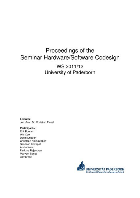
Proceedings of the Seminar Hardware/Software Codesign
Proceedings of the Seminar Hardware/Software Codesign
Proceedings of the Seminar Hardware/Software Codesign

Create successful ePaper yourself
Turn your PDF publications into a flip-book with our unique Google optimized e-Paper software.
<strong>Proceedings</strong> <strong>of</strong> <strong>the</strong><br />
<strong>Seminar</strong> <strong>Hardware</strong>/S<strong>of</strong>tware <strong>Codesign</strong><br />
Lecturer:<br />
Jun.-Pr<strong>of</strong>. Dr. Christian Plessl<br />
Participants:<br />
Erik Bonner<br />
Wei Cao<br />
Denis Dridger<br />
Christoph Kleineweber<br />
Sandeep Korrapati<br />
André Koza<br />
Pavithra Rajendran<br />
Maryam Sanati<br />
Gavin Vaz<br />
WS 2011/12<br />
University <strong>of</strong> Paderborn
Contents<br />
1 An Introduction to Automatic Memory Partitioning<br />
Erik Bonner . . . . . . . . . . . . . . . . . . . . . . . . . . . . . . . . . . 1<br />
2 Error Detection Technique and its Optimization for Real-Time Embedded<br />
Systems<br />
Wei Cao . . . . . . . . . . . . . . . . . . . . . . . . . . . . . . . . . . . . . 17<br />
3 CPU vs. GPU: Which One Will Come Out on Top? Why There is no<br />
Simple Answer<br />
Denis Dridger . . . . . . . . . . . . . . . . . . . . . . . . . . . . . . . . . 32<br />
4 Will Dark Silicon Limit Multicore Scaling?<br />
Christoph Kleineweber . . . . . . . . . . . . . . . . . . . . . . . . . . . . 52<br />
5 Guiding Computation Accelerators to Performance Optimization Dynamically<br />
Sandeep Korrapati . . . . . . . . . . . . . . . . . . . . . . . . . . . . . . . 66<br />
6 A Case for Lifetime-Aware Task Mapping in Embedded Chip Multiprocessors<br />
André Koza . . . . . . . . . . . . . . . . . . . . . . . . . . . . . . . . . . . 80<br />
7 Warp processing<br />
Maryam Sanati . . . . . . . . . . . . . . . . . . . . . . . . . . . . . . . . 98<br />
8 Performance Modeling <strong>of</strong> Embedded Applications with Zero Architectural<br />
Knowledge<br />
Pavithra Rajendran . . . . . . . . . . . . . . . . . . . . . . . . . . . . . . 109<br />
9 Improving Application Launch Times<br />
Gavin Vaz . . . . . . . . . . . . . . . . . . . . . . . . . . . . . . . . . . . . 122<br />
ii
An Introduction to Automatic Memory Partitioning<br />
Erik Bonner<br />
University <strong>of</strong> Paderborn<br />
berik@mail.uni-paderborn.de<br />
January 12, 2012<br />
Abstract<br />
This paper presents Automatic Memory Partitioning, a method for automatically<br />
increasing a program’s data parellism splitting by splitting its data structures into<br />
segments and assigning <strong>the</strong>m to separate, simultaneously accessible memory banks.<br />
Unlike o<strong>the</strong>r data optimization methods, Automatic Memory Partitioning uses dynamic<br />
analysis methods to identify partitionable memory. After partitioning, <strong>the</strong> set<br />
<strong>of</strong> partitioned memory regions is assigned to a set <strong>of</strong> available memory banks by<br />
solving a budgeted graph colouring problem by means <strong>of</strong> Integer Linear Programming<br />
(ILP). After introducing Automatic Memory Partitioning, this paper <strong>of</strong>fers a<br />
discussion on its merits and pitfalls.<br />
1 Introduction<br />
Field Programmable Gate-Arrays (FPGAs) and o<strong>the</strong>r embedded systems can organize<br />
memory into multiple memory banks, which can be accessed simultaneously. Since many<br />
applications are memory-bound, organizing memory into separate memory banks such<br />
that data parallelism is increased during execution can be a powerful means <strong>of</strong> improving<br />
program performance. Consider, for example, <strong>the</strong> code in Listing 1. If all memory were<br />
organized in a single memory bank, and <strong>the</strong> latency for a read were a single clock cycle,<br />
3 clock cycles would be necessary to access <strong>the</strong> memory required to compute <strong>the</strong> result<br />
sum. If, however, each <strong>of</strong> <strong>the</strong> arrays a, b and c were stored in seperate memory banks,<br />
<strong>the</strong> necessary result could be obtained in a single clock cycle.<br />
1 f o r ( i n t i = 0 ; i < ARRAY_SIZE ; i ++)<br />
2 sum [ i ] = a [ i ] + b [ i ] + c [ i ] ;<br />
Listing 1: An example <strong>of</strong> code that benefits from memory parallelization. Listing source:<br />
[3].<br />
2
Erik Bonner<br />
Arrays <strong>of</strong> data structures are <strong>of</strong>ten linearly traversed and, in each iteration, several<br />
components are accessed in <strong>the</strong> same basic block. An example is given in Listing 2. Two<br />
for-loops traverse an array <strong>of</strong> structs <strong>of</strong> type point3d, accessing all three fields x, y<br />
and z in each iteration. When serviced by a single memory bank, extracting <strong>the</strong> contents<br />
<strong>of</strong> each point3d object will have a latency <strong>of</strong> 3 cycles. However, if <strong>the</strong> contents <strong>of</strong> each<br />
point object can be distributed across several different memory banks, each position<br />
extraction can be performed in a single clock cycle.<br />
1 void f i n d _ s t a r s h i p ( p o i n t ∗ s t a r s , i n t n , p o i n t 3 d ∗ ship ,<br />
2 i n t m, i n t ∗ a v a i l )<br />
3 {<br />
4 i n t sx =0 , sy =0 , sz =0 , b =0;<br />
5<br />
6 / / f i n d g a l a x y c e n t e r<br />
7 f o r ( i n t i =0; i
An Introduction to Automatic Memory Partitioning<br />
Figure 1: An example <strong>of</strong> <strong>the</strong> memory used in Listing 1 paritioned and distributed across<br />
3 memory banks. Figure inspired by a similar diagram in [3].<br />
Memory Partitioning identifies seperately accessed memory regions and, by solving a<br />
budgeted graph-colouring algorithm using Integer Linear Programming, assigns (partitions)<br />
<strong>the</strong>m to a mimial set <strong>of</strong> memory banks (see Section 3.2). The particular focus <strong>of</strong><br />
this technique is <strong>the</strong> splitting <strong>of</strong> complex data structures into <strong>the</strong>ir constituent fields and<br />
assigning <strong>the</strong>m to different memory banks, thus greatly accelerating code similar to <strong>the</strong><br />
example given in Listing 2.<br />
After <strong>the</strong> introduction to <strong>the</strong> problem addressed by Automatic Memory Partitioning<br />
given in this section, Section 2 discusses current approaches to memory parallelization<br />
in <strong>the</strong> Literature. Section 3 <strong>the</strong>n discusses <strong>the</strong> Automatic Partitioning Method in detail.<br />
The evaluation results reported by <strong>the</strong> technique authors, Asher and Ro<strong>the</strong>m [3], are given<br />
in Section 4. Finally, critical discussion is provided in Section 5, before <strong>the</strong> paper is<br />
concluded in Section 6.<br />
2 Related Work<br />
A number <strong>of</strong> memory reshaping and partitioning techniques have been proposed in <strong>the</strong><br />
Literature for improving application performance. The majority <strong>of</strong> <strong>the</strong>se are based on<br />
static analysis <strong>of</strong> application source code, i.e analysis that can be performed at compile<br />
time.<br />
Zhao et al. [9] proposed Forma, which is an automatic data reshaping technique performed<br />
(transparently to <strong>the</strong> programmer) at compile time. The aim <strong>of</strong> Forma is to reshape<br />
arrays <strong>of</strong> structs in order to improve data locality and <strong>the</strong>reby optimize cache usage. For<br />
example, consider <strong>the</strong> code given in Listing 3. The for-loop on lines 3-6 traverses an array<br />
<strong>of</strong> point3d objects, accessing only <strong>the</strong> .x field in each iteration. If left unmodified,<br />
running <strong>the</strong> code in Listing 3 results in poor cache performance. Although only <strong>the</strong> .x<br />
field is used in each iteration, due to <strong>the</strong>ir proximity in memory to <strong>the</strong> .x field, <strong>the</strong> .y<br />
and .z fields <strong>of</strong> each structure element will also be fetched to cache, causing significant<br />
cache clutter.<br />
4
Erik Bonner<br />
1 / / compute a v e r a g e x c o o r d i n a t e<br />
2 i n t sumx = 0 , avg = 0 ;<br />
3 f o r ( i n t i = 0 ; i < NUM_STARS; i ++)<br />
4 {<br />
5 sumx += s t a r s [ i ] . x ;<br />
6 }<br />
7 avg = sumx /NUM_STARS;<br />
Listing 3: Code suitable for optimization with Forma.<br />
By combining statistics ga<strong>the</strong>red from execution pr<strong>of</strong>iling, which identify <strong>the</strong> usage<br />
frequency and affinity <strong>of</strong> <strong>the</strong> structure fields, with static code analysis, data structure object<br />
fields in Listing 3 can be partitioned and <strong>the</strong> stars array reshaped to support <strong>the</strong><br />
data locality present in <strong>the</strong> program execution. Figure 2 shows how <strong>the</strong> stars array<br />
could be reshaped to improve cache performance. Although Forma is primarily targeted<br />
at devices with traditional memory heirarchies, <strong>the</strong> data structure partitioning and array<br />
reshaping used can be adapted to target platforms with multiple memory banks.<br />
Figure 2: An example <strong>of</strong> reshaping an array <strong>of</strong> point3d objects using Forma. Using <strong>the</strong><br />
restructured array, <strong>the</strong> traversal in Listing 3 would enjoy a significantly improved cache<br />
performance.<br />
Lattner and Adve et al. [7] proposed a technique called Automatic Pool Allocation,<br />
which, by means <strong>of</strong> static pointer analysis, improves performance <strong>of</strong> heap-based data<br />
structures (such as linked-lists or trees) by partitioning allocation <strong>of</strong> individual complex<br />
objects into different memory pools. For example, <strong>the</strong> nodes in a linked list can be automatically<br />
allocated in different memory pools. By controlling allocation <strong>of</strong> objects within<br />
pools, <strong>the</strong> compiler can ensure that memory can be structured in an aligned format, which<br />
greatly improves data locality. Figure 3 compares <strong>the</strong> memory structure <strong>of</strong> a linked-list<br />
allocated using traditional allocators (such as malloc()) with one whose nodes have<br />
5
An Introduction to Automatic Memory Partitioning<br />
been allocated using Automatic Pool Allocation. Since <strong>the</strong> linked-list nodes are not scattered<br />
throughout memory in <strong>the</strong> latter example, a traversal <strong>of</strong> <strong>the</strong> linked-list will benefit<br />
from improved cache performance.<br />
(a) (b)<br />
Figure 3: An example <strong>of</strong> Automatic Pool Allocation. The figure on <strong>the</strong> left (a) shows a set<br />
<strong>of</strong> nodes belonging to a linked list, allocated using traditional methods in main memory.<br />
The nodes are scattered randomly throughout memory. The figure on <strong>the</strong> right (b) shows<br />
<strong>the</strong> same nodes allocated using Automatic Pool Allocation. Using this method, new nodes<br />
are allocated in so-called “pools”, which are dedicated memory regions ensuring contiguous<br />
node allocation.<br />
Like Forma, Automatic Pool Allocation is a static technique primarily intended for<br />
use during compilation for traditional, heirarchy-based memory architectures. However,<br />
also like Forma, Automatic Pool Allocation can be readily adapted to architectures using<br />
multiple memory banks.<br />
Curial et al. [5] proposed a method called MPADS (Memory-Pooling-Assisted Data<br />
Splitting), which can be considered a combination <strong>of</strong> Forma and Automatic Pool Allocation.<br />
Using this method, individual objects <strong>of</strong> complex data structure types are split among<br />
memory pools. In this aspect, MPADS <strong>of</strong>fers very similar functionality to <strong>the</strong> Automatic<br />
Memory Partitioning technique described in this paper. Unlike Automatic Memory Paritioning,<br />
however, MPADS accomplishes its memory splitting and allocation purely using<br />
static code analysis, which, <strong>the</strong>y argue, has <strong>the</strong> advantage <strong>of</strong> avoiding <strong>the</strong> generation <strong>of</strong><br />
large memory traces. On <strong>the</strong> o<strong>the</strong>r hand, MPADS is designed for use with commercial<br />
compilers, and <strong>the</strong>refore must be more minimalistic and pessimistic in its approach than<br />
o<strong>the</strong>r, research specific methods. For example, if <strong>the</strong>re is a chance that a potential memory<br />
transformation could modify <strong>the</strong> semantics <strong>of</strong> <strong>the</strong> target program, <strong>the</strong> transformation<br />
is abandoned.<br />
The main contribution <strong>of</strong> Automatic Memory Paritioning, which is not addressed by<br />
<strong>the</strong> related work, is a combination <strong>of</strong> data structure partitioning and dynamic code analysis.<br />
This entails analysing <strong>the</strong> program according to its dynamic behaviour, ra<strong>the</strong>r than<br />
6
Erik Bonner<br />
analysing its code statically at compile time. The pros and cons <strong>of</strong> using this approach are<br />
discussed in Section 5.<br />
3 Proposed Technique<br />
Automatic Memory Partitioning is a technique for optimizing linear traversal <strong>of</strong> data<br />
structure arrays on embedded devices (primarily FPGAs) that organize memory in a<br />
set <strong>of</strong> simultaneously accessible memory banks. By automatically partitioning program<br />
data structures such that individual structure components are placed in different memory<br />
banks, linear traversals <strong>of</strong> data structure arrays are significantly accelerated (see <strong>the</strong><br />
example in Section 1).<br />
Automatic Memory Partitioning consists <strong>of</strong> two main stages: identifying <strong>the</strong> set <strong>of</strong> disjoint<br />
memory access patterns within a program/kernel execution, and assigning memory<br />
regions to a minimal set <strong>of</strong> memory banks. These techniques are described in Sections<br />
3.1 and 3.2, respectively. Once memory has been redistributed into banks, all pointers<br />
accessing this memory must be updated. This process is described in Section 3.3.<br />
3.1 Linear Memory Pattern decomposition<br />
3.1.1 Linear Memory Patterns (LMPs)<br />
The first step in <strong>the</strong> proposed method is to decompose <strong>the</strong> overall memory signature <strong>of</strong><br />
a program execution into a set (lp0, ..., lpk) <strong>of</strong> disjunct Linear Memory Patterns (LMPs),<br />
where:<br />
• Each load in <strong>the</strong> code is associated with an LMP lpi.<br />
• Each LMP lpi represents a set <strong>of</strong> sequentially spaced memory addresses <strong>of</strong> <strong>the</strong> form<br />
αx + β, where β is <strong>the</strong> <strong>of</strong>fset <strong>of</strong> <strong>the</strong> first memory access, α <strong>the</strong> stride separating<br />
adjacent accesses and x an integer between 0 and some upper bound n.<br />
• Each memory operation in <strong>the</strong> program is mapped to exactly one LMP, which spans<br />
all memory addresses associated with that operation’s signature.<br />
3.1.2 Memory pr<strong>of</strong>iling<br />
Unlike <strong>the</strong> memory partitioning methods discussed in Section 2, <strong>the</strong> set <strong>of</strong> LMPs existing<br />
in a program’s memory signature is identified by means <strong>of</strong> dynamic program analysis.<br />
To obtain <strong>the</strong> memory trace <strong>of</strong> an execution, <strong>the</strong> program source code is instrumented<br />
such that a call to a custom function is inserted immediately prior to each memory operation<br />
opcode. When <strong>the</strong> instrumented binary is executed, <strong>the</strong> custom functions write <strong>the</strong><br />
identifier and operand address(es) <strong>of</strong> each memory operator to a log on disk. After execution,<br />
<strong>the</strong> contents <strong>of</strong> <strong>the</strong> log make up a complete memory trace <strong>of</strong> <strong>the</strong> program execution.<br />
Figure 4 shows a portion <strong>of</strong> a sample memory trace log.<br />
7
An Introduction to Automatic Memory Partitioning<br />
Figure 4: An example memory trace log. Image source [3].<br />
The example trace in Figure 4 logs four op codes (referred to as #7, #12, #17 and #22)<br />
consecutively operating on <strong>the</strong> fields <strong>of</strong> an array <strong>of</strong> adjacently allocated data structure<br />
objects. The address upon which each op code operates is given in <strong>the</strong> left-most table<br />
column, and <strong>the</strong> basic block to which <strong>the</strong>y belong is specified in <strong>the</strong> right-most column.<br />
3.1.3 Data structure decomposition<br />
Once <strong>the</strong> memory trace <strong>of</strong> an execution has been generated, it is analysed to determine a<br />
set <strong>of</strong> LMPs that can correctly represent <strong>the</strong> program memory pr<strong>of</strong>ile. For <strong>the</strong> analysis, an<br />
LMP is defined as a 4-tuple Rl, Rh, Op, S, where Rl and Rh define <strong>the</strong> upper and lower<br />
bounds on <strong>the</strong> memory range, repectivley; Op defines a set <strong>of</strong> memory operations that<br />
operate on addresses within this range; and S, which corresponds to α in Section 3.1.1,<br />
defines <strong>the</strong> stride between each potential access.<br />
Listing 4 shows an example code snippet for looping through an array <strong>of</strong> point3d<br />
objects and accessing <strong>the</strong> .x structure field. Since <strong>the</strong> array <strong>of</strong> structs is allocated as<br />
a contigious memory region <strong>of</strong> adjacent struct elements, each read <strong>of</strong> <strong>the</strong> .x field is<br />
seperated by a distance <strong>of</strong> size<strong>of</strong>(point) bytes. Fur<strong>the</strong>rmore, since <strong>the</strong> memory<br />
operation applied to this field is alternating between reading and writing, <strong>the</strong> LMP propery<br />
Op contains both read and write opcodes. Finally, <strong>the</strong> memory range defined by Rl and<br />
Rh spans 100*size<strong>of</strong>(point) bytes. The diagram in Figure 5 visualizes <strong>the</strong> LMP,<br />
denoted lp0, constructed from <strong>the</strong> code in Listing 4.<br />
1 p o i n t 3 d p a r r a y [ 1 0 0 ] ;<br />
2 f o r ( i n t i = 0 ; i < 100; i ++)<br />
3 {<br />
4 i f ( i%2 == 0)<br />
5 do_some_computation ( p a r r a y [ i ] . x ) ;<br />
6 e l s e<br />
8
Erik Bonner<br />
7 p a r r a y [ i ] . x = s o m e _ o t h e r _ c o m p u t a t i o n ( ) ;<br />
8 }<br />
Listing 4: Simple code for looping through an array <strong>of</strong> structs, alternating between reading<br />
and writing.<br />
Figure 5: A view <strong>of</strong> memory during <strong>the</strong> execution <strong>of</strong> <strong>the</strong> code in Listing 3. An LMP, lp0,<br />
can be constructed to represent <strong>the</strong> accesses to <strong>the</strong> field parray[i].x (marked in yellow).<br />
The LMP range, Rl and Rh; set <strong>of</strong> operations, Op; and stride, S, which is this case is<br />
equal to size<strong>of</strong>(point3d), are marked in <strong>the</strong> diagram.<br />
The pseudocode given in Figure 6 demonstrates how <strong>the</strong> set <strong>of</strong> LMPs for a given<br />
program execution can be extracted from its memory trace. The first loop, on Lines 1<br />
to 11, creates an LMP for each opcode in <strong>the</strong> set <strong>of</strong> all identified opcodes found in <strong>the</strong><br />
memory trace. Note that this part <strong>of</strong> <strong>the</strong> algorithm can be performed online, while <strong>the</strong><br />
memory trace is being generated. The second loop compares each identified LMP with<br />
all o<strong>the</strong>r identified LMPs to determine if any two can be merged. Two LMPs can be<br />
merged if <strong>the</strong>y operate on common memory cells. This will be true for two candidate<br />
LMPs if both <strong>of</strong> <strong>the</strong> following conditions hold:<br />
1. There is an intersection <strong>of</strong> <strong>the</strong> candidate ranges.<br />
2. Both candidates have <strong>the</strong> same <strong>of</strong>fset within <strong>the</strong>ir stride.<br />
When traversing an array <strong>of</strong> complex data types, <strong>the</strong> traversal stride represents <strong>the</strong><br />
size <strong>of</strong> <strong>the</strong> complex data type object, and <strong>the</strong> <strong>of</strong>fset within <strong>the</strong> stride indicates which<br />
field within <strong>the</strong> data structure is being accessed. For example, consider two functions:<br />
compute_x() and compute_y(). The function body <strong>of</strong> compute_x() is made <strong>of</strong><br />
up <strong>of</strong> <strong>the</strong> code given in Listing 4, while <strong>the</strong> body <strong>of</strong> compute_y() is nearly identical to<br />
that <strong>of</strong> compute_x(), with <strong>the</strong> exception that it operates on <strong>the</strong> parray[i].y field.<br />
The LMPs extracted from <strong>the</strong> traces <strong>of</strong> <strong>the</strong>se functions would have indentical strides and<br />
largely overlapping ranges. However, since <strong>the</strong>y are accessing different elements <strong>of</strong> <strong>the</strong><br />
point3d data structure, <strong>the</strong> <strong>of</strong>fset within <strong>the</strong>ir strides differ. Therefore, <strong>the</strong> LMPs <strong>of</strong> <strong>the</strong><br />
compute_x() and compute_y() functions will not be mergable.<br />
9
An Introduction to Automatic Memory Partitioning<br />
Two candidate LMPs are merged by setting <strong>the</strong> merged range to <strong>the</strong> minimum and<br />
maximum <strong>of</strong> <strong>the</strong>ir respective upper and lower range bounds, setting <strong>the</strong> LMP Op field to<br />
<strong>the</strong> union <strong>of</strong> <strong>the</strong> both candidate Ops and setting <strong>the</strong> merged stride to <strong>the</strong> greatest common<br />
devisor <strong>of</strong> <strong>the</strong> two candidate strides. After <strong>the</strong> second nested loop (Lines 12-23), <strong>the</strong><br />
set <strong>of</strong> disjoint LMPs present in program execution has been identified and is ready for<br />
assignment to <strong>the</strong> available memory banks.<br />
Figure 6: The algorithm used for extracting a set <strong>of</strong> LMPs from a memory trace. Image<br />
source [3].<br />
3.2 Memory bank allocation<br />
Once <strong>the</strong> set <strong>of</strong> LMPs present during execution have been identified, <strong>the</strong> memory referenced<br />
by each LMP must be assigned to memory banks in an optimal manner. In order<br />
to accomplish this, <strong>the</strong> set <strong>of</strong> LMPs must be assigned to a set <strong>of</strong> K memory banks with<br />
known capacities, such that:<br />
• Maximum memory parallelism can be achieved.<br />
• The capacity <strong>of</strong> each memory bank is sufficient to store all LMPs assigned to it.<br />
• A minimal number <strong>of</strong> banks are used.<br />
10
Erik Bonner<br />
The optimal assignment <strong>of</strong> LMPs to memory banks is attained by solving a modified<br />
graph colouring problem. The traditional graph colouring problem is formulated as follows.<br />
Given a graph G = (V, E), where V is a set <strong>of</strong> vertices and E is <strong>the</strong> set <strong>of</strong> edges<br />
connecting <strong>the</strong>m, a mapping φ : V → C is sought such that ∀(u, v) ∈ G, c(u) �= c(v),<br />
where <strong>the</strong> function c() assigns a “colour” to each vertex. In o<strong>the</strong>r words, given a graph,<br />
<strong>the</strong> graph colouring problem involves assigning a set <strong>of</strong> colours (or generally, some value)<br />
to <strong>the</strong> graph vertices such that no adjacent vertices are assigned <strong>the</strong> same colour. For <strong>the</strong><br />
assignment <strong>of</strong> LMPs to memory banks, <strong>the</strong> set <strong>of</strong> LMPs are <strong>the</strong> graph vertices and <strong>the</strong><br />
set <strong>of</strong> memory banks are <strong>the</strong> assignable colours. Two vertices are connected by an edge<br />
if <strong>the</strong>ir LMPs cannot be assigned to <strong>the</strong> same memory bank. Fur<strong>the</strong>rmore, an additional<br />
constraint is added to <strong>the</strong> problem: each LMP, or vertex, has an associated size, and each<br />
bank, or colour, has a limited capacity. LMPs must be assigned to banks such that no<br />
bank has its capacity exceeded. This is known as a budgeted graph colouring problem.<br />
Figure 7 shows a simple example <strong>of</strong> <strong>the</strong> budgeted graph colouring problem, solved for a<br />
set <strong>of</strong> 5 nodes and 3 colours.<br />
Figure 7: An example <strong>of</strong> a solved budgeted graph colouring problem. Each node has an<br />
associated size value and each colour has an associated capacity. Nodes must be assigned<br />
to colours such that <strong>the</strong> total size <strong>of</strong> all nodes assigned to a given colour does not exceed<br />
that colour’s capacity. Figure redrawn from [3].<br />
Generally, <strong>the</strong> problem <strong>of</strong> graph colouring is NP-complete [6]. A common problem<br />
for which graph colouring is used is <strong>the</strong> assignment <strong>of</strong> variables to registers in compilers<br />
[4]. Accordingly, a number <strong>of</strong> heuristic-based solution strategies have been proposed.<br />
In Automatic Memory Partitioning, <strong>the</strong> memory bank allocation problem is solved using<br />
Integer Linear Programming (ILP). Budgeted graph colouring is structured with an ILP<br />
problem as follows. For n LMPs and m memory banks, a set <strong>of</strong> mxn boolean variables are<br />
defined such that <strong>the</strong> variable xij is 1 if LMP i is assigned to memory bank j. Fur<strong>the</strong>rmore,<br />
for each memory bank, a boolean variable cj indicates whe<strong>the</strong>r that memory bank is<br />
currently being used. By minimizing (c0, ..., cm) subject to a number <strong>of</strong> constraints, an<br />
optimal bank allocation can be found. The minimization constraints are defined as:<br />
• Each LMP is assigned to exactly one memory bank:<br />
∀i( � m j=0 xij ≥ 1 and � m j=0 xij ≤ 1)<br />
11
• No memory bank is overfilled:<br />
∀j � n i=0 xij ∗ size<strong>of</strong>(LMPi) ≤ size<strong>of</strong>(bankj)<br />
An Introduction to Automatic Memory Partitioning<br />
• Confilicting LMPs cannot be assigned to <strong>the</strong> same bank:<br />
∀j(xvj + xwj) ≤ 1, where v and w are conflicting LMPs.<br />
The above ILP problem is solved using <strong>the</strong> freeware CVXOPT s<strong>of</strong>tware package.<br />
3.3 Pointer syn<strong>the</strong>sis<br />
Once memory has been correctly rearranged into a minimal set <strong>of</strong> memory banks, all<br />
pointers in <strong>the</strong> target program accessing this memory must be reassigned accordingly.<br />
Consider <strong>the</strong> memory bank depicted in Figure 8, which contains three LMPs. In original<br />
memory, each LMP has an associated starting address (Rl), size (Rh − Rl) and stride<br />
(S). When assigned to a memory bank, <strong>the</strong>se LMP properties must be updated such that<br />
memory is correctly addressed within <strong>the</strong> assigned bank.<br />
Figure 8: A single memory bank with three LMPs (lpi, lpj and lpk) assigned to it. Each<br />
LMP has an associated size and <strong>of</strong>fset within <strong>the</strong> bank.<br />
For each pointer Pold that accesses <strong>the</strong> LMP in original memory, <strong>the</strong> following steps<br />
are taken to determine its new value Pnew within <strong>the</strong> assigned memory bank. First, <strong>the</strong><br />
start address Rl is subtracted from Pold. Then, since <strong>the</strong> memory accessed by each LMP<br />
will be packed into <strong>the</strong> assigned memory bank linearly, <strong>the</strong> final LMP stride must be<br />
adjusted. This is accomplished by scaling each old pointer value by a factor ˆs, where ˆs<br />
is a multiple its LMP stride. Finally, <strong>the</strong> starting address ˆ b <strong>of</strong> <strong>the</strong> LMP within its newly<br />
assigned memory bank must be added. The complete pointer mapping is given by:<br />
�<br />
Pold − Rl<br />
Pnew =<br />
ˆs<br />
+ ˆ � �<br />
Pold Rl<br />
b = −<br />
ˆs ˆs + ˆ � � �<br />
Pold<br />
b = ± C<br />
ˆs<br />
where C is a constant for each LMP. The most expensive part <strong>of</strong> this mapping is <strong>the</strong><br />
operation Pold . However, when ˆs is a power <strong>of</strong> two, this can be implemented using bit-<br />
ˆs<br />
shifting, which is a cheap operation on FPGAs.<br />
4 Reported Results<br />
Automatic Memory Partitioning performance was evaluated by syn<strong>the</strong>sising a collection<br />
<strong>of</strong> memory-intensive programs from <strong>the</strong> NVIDIA CUDA SDK [8], CLAPACK SDK [1]<br />
and SystemRacer test suite [2]. The samples were syn<strong>the</strong>sized with single, as well as<br />
12
Erik Bonner<br />
(a) (b)<br />
Figure 9: Evaluation. The table on <strong>the</strong> left (a) lists <strong>the</strong> name <strong>of</strong> each test program (left<br />
column), <strong>the</strong> number <strong>of</strong> cycles per iteration when using a single memory bank (centerleft<br />
column) and multiple memory banks (center-right column), as well as <strong>the</strong> number <strong>of</strong><br />
memory banks used for Automatic Memory Partitioning (right column). These results are<br />
visualized in <strong>the</strong> graph on <strong>the</strong> right (b). Images from [3].<br />
.<br />
multiple memory banks, and <strong>the</strong> resulting performances were compared. All programs<br />
were syn<strong>the</strong>sized to Verilog using <strong>the</strong> SystemRacer syn<strong>the</strong>sis engine. Each memory bank<br />
was syn<strong>the</strong>sized with a single memory port and each memory port had a latency <strong>of</strong> 3<br />
cycles. A comparison <strong>of</strong> <strong>the</strong> performance measured for <strong>the</strong> test programs syn<strong>the</strong>sized<br />
with a single vs. multiple memory banks is given in Figure 9.<br />
In most cases, it was possible to syn<strong>the</strong>size <strong>the</strong> target code using more than one memory<br />
bank. In all such cases, performance improvements were recorded when running <strong>the</strong><br />
multiple bank versions. As can be expected, <strong>the</strong> more banks used, <strong>the</strong> greater <strong>the</strong> memory<br />
parallelism, and hence <strong>the</strong> greater <strong>the</strong> performance gains.<br />
5 Discussion<br />
This section provides additional discussion and remarks regarding <strong>the</strong> Automatic Memory<br />
Partitioning method.<br />
In <strong>the</strong> original paper by Asher et al. [3] it is claimed that, unlike previously existing<br />
methods, Automatic Memory Partitioning performs memory optimization by means <strong>of</strong><br />
dynamic analysis. Although this is true, <strong>the</strong>re are some significant limitations. A target<br />
application’s memory is partitioned based on an analysis <strong>of</strong> its memory trace, generated<br />
during a pr<strong>of</strong>iling run. For <strong>the</strong> method to work, it is necessary that memory addresses<br />
and usage are indentical between runs. For many applications, particularly those whose<br />
control flow is data-dependent, this means that <strong>the</strong> memory partitioning will only work<br />
on <strong>the</strong> exact input for which <strong>the</strong> memory trace was generated. Fur<strong>the</strong>rmore, to ensure<br />
that memory will be located in <strong>the</strong> same place between runs, <strong>the</strong> method relies on <strong>the</strong> use<br />
13
An Introduction to Automatic Memory Partitioning<br />
<strong>of</strong> custom memory allocators, ra<strong>the</strong>r than traditional functions such as malloc() that<br />
intentionally randomize memory allocation locations for security reasons. Since such<br />
allocators allocate memory in a predefined, predictable manner that is persistent between<br />
runs, a program using <strong>the</strong>se allocators can also be correctly analysed using static analysis.<br />
This weakens <strong>the</strong> claim that, by using dynamic analysis techniques, Automatic Memory<br />
Partitioning achieves results that are not obtainable using static methods.<br />
Ano<strong>the</strong>r point <strong>of</strong> discussion is <strong>the</strong> reported results. As discussed in Section 4, results<br />
were ga<strong>the</strong>red by syn<strong>the</strong>sizing a collection <strong>of</strong> sample programs with a single memory<br />
bank, and comparing performance with <strong>the</strong> same programs syn<strong>the</strong>sized with multiple<br />
memory banks. Clearly, <strong>the</strong> programs syn<strong>the</strong>sized with multiple memory banks outperformed<br />
those with single memory banks. This is more a pro<strong>of</strong> that <strong>the</strong> method works,<br />
ra<strong>the</strong>r than that it works well. Far more interesting would have been a comparison between<br />
sample programs optimized with Automatic Memory Partiotioning with those optimized<br />
using o<strong>the</strong>r methods in <strong>the</strong> Literature, such as MPADS. Fur<strong>the</strong>rmore, a number<br />
<strong>of</strong> <strong>the</strong> samples that were used from <strong>the</strong> CUDA SDK are already hand-optimized to use<br />
multiple (shared) memory banks. Syn<strong>the</strong>sizing <strong>the</strong>se to use a single memory bank would<br />
involve significant modifications to <strong>the</strong> original source code, with <strong>the</strong> explicit goal <strong>of</strong> reducing<br />
performance. When syn<strong>the</strong>sized for use with multiple memory banks, did <strong>the</strong>y<br />
use <strong>the</strong> modified, single-bank code, or <strong>the</strong> original SDK sample, written with a multiple<br />
memory bank archtecture in mind? In <strong>the</strong> paper, this is not clear.<br />
In addition to <strong>the</strong> performance <strong>of</strong> <strong>the</strong> syn<strong>the</strong>sized application, <strong>the</strong> performance <strong>of</strong> <strong>the</strong><br />
Automatic Memory Partioning procedure itself is also <strong>of</strong> interest. Discussion <strong>of</strong> this is<br />
largely left out <strong>of</strong> <strong>the</strong> original paper. Both <strong>the</strong> major phases <strong>of</strong> Automatic Memory Paritioning<br />
- memory partitioning and assignment <strong>of</strong> memory regions to available memory<br />
banks - can potentially be slow under <strong>the</strong> right circumstances. The partitioning <strong>of</strong> data<br />
structures relies on <strong>the</strong> use <strong>of</strong> execution traces, which could potentially become very large,<br />
particulalry for applications that process large amounts <strong>of</strong> data and contain frequent datadependent<br />
branching. The authors <strong>of</strong> <strong>the</strong> MPADS method (described in Section 2) explicitly<br />
state <strong>the</strong> importance <strong>of</strong> avoiding execution traces when performance is a concern [5].<br />
Fur<strong>the</strong>rmore, when <strong>the</strong> number <strong>of</strong> identified LMPs becomes large, <strong>the</strong> task <strong>of</strong> assigning<br />
memory banks becomes increasingly complex. In Automatic Memory Partitioning, this<br />
task is formulated as an ILP problem and solved using a heuristic solver. They reported<br />
speeds <strong>of</strong> under a second for a set <strong>of</strong> 10 LMPs. It would be interesting to see performance<br />
for larger LMP sets. Fur<strong>the</strong>rmore, it would be interesting to know how many LMPs can<br />
be expected when syn<strong>the</strong>sising larger programs.<br />
One advantage <strong>of</strong> using memory traces as <strong>the</strong> sole basis for memory analysis is <strong>the</strong> relative<br />
simplicity <strong>of</strong> <strong>the</strong> method. Static techniques <strong>of</strong>ten need to employ complex, language<br />
dependent pointer analysis, with additional measures for type-unsafe languages such as<br />
C and C++. By analysing <strong>the</strong> memory trace, ra<strong>the</strong>r than <strong>the</strong> code itself, <strong>the</strong>se complex<br />
methods can be avoided. Moreover, using memory traces allows <strong>the</strong> memory analysis<br />
method to be more language independent; Automatic Memory Partitioning can easily be<br />
used for any language that can be instrumented to generate suitable memory trace logs.<br />
On <strong>the</strong> o<strong>the</strong>r hand, <strong>the</strong> generation and analysis <strong>of</strong> memory traces can be a cumbersome<br />
14
Erik Bonner<br />
process, since <strong>the</strong>y can become very large.<br />
6 Conclusion<br />
This paper introduced a technique for automatically partitioning data structures across<br />
multiple memory banks on embedded devices such as FPGAs, which enhances application<br />
performance by increasing memory parallelism.<br />
After using a number <strong>of</strong> simple examples in Section 1 to illustrate <strong>the</strong> advantages<br />
<strong>of</strong> memory partitioning on architectures with simultaneously accessible memory banks, a<br />
number <strong>of</strong> relevant data partitioning methods currently existing in <strong>the</strong> Literature were discussed<br />
in Section 2. Although a number <strong>of</strong> <strong>the</strong> existing methods show promising results,<br />
all rely on static code analysis to identify memory partitioning opportunities. Following<br />
<strong>the</strong> literature review, Section 3 moved on to introduce a memory optimization technique<br />
that uses dynamic analysis: Automatic Memory Partitioning. Automatic Memory Partioning<br />
indentifies a target program’s memory access patterns by analysing its memory<br />
trace. Once a set <strong>of</strong> non-interfering memory access patterns have been identified, <strong>the</strong>y<br />
are assigned to a set <strong>of</strong> memory banks, taking care to minimize <strong>the</strong> number <strong>of</strong> banks used<br />
while maximimizing data parallelism. The results reported by <strong>the</strong> authors <strong>of</strong> <strong>the</strong> technique<br />
were given in Section 4. Finally, Section 5 <strong>of</strong>fered a critical disussion <strong>of</strong> <strong>the</strong> Automatic<br />
Memory Partitioning techique, evaluating its strengths and weaknesses.<br />
References<br />
[1] E. Anderson, Z. Bai, C. Bisch<strong>of</strong>, S. Blackford, J. Demmel, J. Dongarra, J. Du Croz,<br />
A. Greenbaum, S. Hammarling, A. McKenney, and D. Sorensen. LAPACK Users’<br />
Guide. Society for Industrial and Applied Ma<strong>the</strong>matics, Philadelphia, PA, third edition,<br />
1999.<br />
[2] Y. Ben-Asher and N. Rotem. Syn<strong>the</strong>sis for variable pipelined function units. In<br />
System-on-Chip, 2008. SOC 2008. International Symposium on, pages 1–4, nov.<br />
2008.<br />
[3] Yosi Ben-Asher and Nadav Rotem. Automatic memory partitioning: increasing<br />
memory parallelism via data structure partitioning. In <strong>Proceedings</strong> <strong>of</strong> <strong>the</strong> eighth<br />
IEEE/ACM/IFIP international conference on <strong>Hardware</strong>/s<strong>of</strong>tware codesign and system<br />
syn<strong>the</strong>sis, CODES/ISSS ’10, pages 155–162, New York, NY, USA, 2010. ACM.<br />
[4] G. J. Chaitin. Register allocation & spilling via graph coloring. SIGPLAN Not.,<br />
17:98–101, June 1982.<br />
[5] Stephen Curial, Peng Zhao, Jose Nelson Amaral, Yaoqing Gao, Shimin Cui, Raul<br />
Silvera, and Roch Archambault. Mpads: memory-pooling-assisted data splitting. In<br />
15
An Introduction to Automatic Memory Partitioning<br />
<strong>Proceedings</strong> <strong>of</strong> <strong>the</strong> 7th international symposium on Memory management, ISMM ’08,<br />
pages 101–110, New York, NY, USA, 2008. ACM.<br />
[6] M. R. Garey and D. S. Johnson. The complexity <strong>of</strong> near-optimal graph coloring. J.<br />
ACM, 23:43–49, January 1976.<br />
[7] Chris Lattner and Vikram Adve. Automatic Pool Allocation: Improving Performance<br />
by Controlling Data Structure Layout in <strong>the</strong> Heap. In <strong>Proceedings</strong> <strong>of</strong> <strong>the</strong> 2005<br />
ACM SIGPLAN Conference on Programming Language Design and Implementation<br />
(PLDI’05), Chigago, Illinois, June 2005.<br />
[8] NVIDIA. Nvidia cuda sdk, 2011.<br />
[9] Peng Zhao, Shimin Cui, Yaoqing Gao, Raúl Silvera, and José Nelson Amaral. Forma:<br />
A framework for safe automatic array reshaping. ACM Trans. Program. Lang. Syst.,<br />
30, November 2007.<br />
16
Error Detection Technique and its Optimization for<br />
Real-Time Embedded Systems<br />
Wei Cao<br />
University <strong>of</strong> Paderborn<br />
wcao@mail.upb.de<br />
January, 12 2012<br />
Abstract<br />
This paper discusses error detection techniques and <strong>the</strong> optimization <strong>of</strong> error detection<br />
implementation(EDI) in <strong>the</strong> context <strong>of</strong> different FPGAs, including FPGA<br />
with static configuration and FPGA with partial dynamic reconfiguration(PDR). In<br />
<strong>the</strong> error detection techniques, path tracking and variable checking are <strong>the</strong> main<br />
sources <strong>of</strong> performance overhead. According to <strong>the</strong>ir different implementation ways,<br />
<strong>the</strong>re are three basic error detection implementations: s<strong>of</strong>tware-only(SW-only) approach,<br />
in which both path tracking and variable checking are implemented in s<strong>of</strong>tware;<br />
mixed s<strong>of</strong>tware/hardware(mixed SW/HW) approach, in which path tracking<br />
leading to significant time overhead is moved into hardware and variable checking<br />
remains in s<strong>of</strong>tware; hardware-only(HW-only) approach, in which both <strong>of</strong> <strong>the</strong>m are<br />
performed in hardware. This paper introduces error detection approaches based on<br />
<strong>the</strong>se basic error detection implementations and discusses <strong>the</strong>m in detail. Fur<strong>the</strong>r<br />
more, considering <strong>the</strong> fact that an application normally consists <strong>of</strong> a number <strong>of</strong> processes,<br />
error detection can be optimized through applying it to every process, i.e.<br />
to achieve <strong>the</strong> efficient implementation <strong>of</strong> error detection through <strong>the</strong> refinement <strong>of</strong><br />
error detection. Therefore, two optimization algorithms are presented in this paper<br />
as well. One optimization algorithm focuses on <strong>the</strong> case <strong>of</strong> FPGA supporting only<br />
static configuration and <strong>the</strong> o<strong>the</strong>r one, on <strong>the</strong> case <strong>of</strong> FPGA supporting PDR. The<br />
improvement after <strong>the</strong> optimization will be shown through experimental results.<br />
1 Introduction<br />
Errors are always unavoidable in any system. If errors are not detected in time, <strong>the</strong>y can<br />
cause result deviations, even program crashes. In <strong>the</strong> context <strong>of</strong> errors, to detect errors is<br />
<strong>the</strong> only possibility to guarantee <strong>the</strong> effectiveness <strong>of</strong> an application’s execution. Therefore,<br />
error detection is indispensable for any system, especially for real-time systems, in<br />
which errors should be not only effectively detected, but also efficiently detected. To<br />
18
Wei Cao<br />
achieve this goal, many error detection techniques have been developed. Each error detection<br />
technique ei<strong>the</strong>r causes a certain number <strong>of</strong> time overheads, or requires a certain<br />
number <strong>of</strong> hardware resources, for some techniques even both. In real-time systems, each<br />
application has a deadline. Because <strong>of</strong> <strong>the</strong> existence <strong>of</strong> deadline, for error detection in<br />
real-time systems, time overhead is a more important factor than hardware cost. Consequently,<br />
<strong>the</strong> time for error detection should be minimized in order to satisfy <strong>the</strong> deadline<br />
<strong>of</strong> <strong>the</strong> application. There are various ways to optimize <strong>the</strong> time for error detection. To determine<br />
an appropriate error detection implementation for each process <strong>of</strong> <strong>the</strong> application<br />
in an intelligent manner is regarded as a considerable way.<br />
The main focus <strong>of</strong> this paper is <strong>the</strong> systematic discussion about error detection technique,<br />
including corresponding approaches and <strong>the</strong> explanation <strong>of</strong> an approach to <strong>the</strong> optimization<br />
<strong>of</strong> error detection implementation.<br />
2 Error Detection Technique<br />
Although <strong>the</strong> traditional approach <strong>of</strong> error detection, so called “one-size-fits-all” approach,<br />
is capable <strong>of</strong> providing a certain error coverage, this error coverage sometimes<br />
can be ra<strong>the</strong>r low and can not meet <strong>the</strong> expected requirements, i.e. <strong>the</strong> traditional approach<br />
is not able to supply sufficient reliability. Since every application has its own<br />
characteristics, <strong>the</strong> reliability provided by error detection can be dramatically improved<br />
if EDI for a specific application can be adjusted according to <strong>the</strong>se characteristics. To<br />
take full advantage <strong>of</strong> characteristics <strong>of</strong> each application, application-aware technique has<br />
been developed.<br />
2.1 Working Principle<br />
The purpose <strong>of</strong> application-aware technique is to improve <strong>the</strong> reliability <strong>of</strong> an application<br />
with <strong>the</strong> help <strong>of</strong> its characteristics, as stated above. Then, next question occurs: How to<br />
implement error detection in application-aware technique? The answer is as follows:<br />
1. The first step is to identify critical variables in a program. A critical variable is<br />
defined as "a program variable that exhibits high sensitivity to random data errors<br />
in <strong>the</strong> application"[6].<br />
2. Once critical variables have been identified, backward program slice, defined as "<strong>the</strong><br />
set <strong>of</strong> all program statements/instructions that can affect <strong>the</strong> value <strong>of</strong> <strong>the</strong> variable at<br />
a program location"[8], can be extracted as <strong>the</strong> second step.<br />
3. After <strong>the</strong> extraction <strong>of</strong> backward program slice, checking expressions are generated<br />
during <strong>the</strong> optimization <strong>of</strong> each slice at compile time. These expressions are<br />
<strong>the</strong>n inserted into <strong>the</strong> original code and will be chosen by checking instructions to<br />
compare <strong>the</strong> results.<br />
19
Error Detection Technique and its Optimization for Real-Time Embedded Systems<br />
Thus, along with <strong>the</strong> execution <strong>of</strong> <strong>the</strong> original code, instructions for tracking control paths<br />
and <strong>the</strong> checking expressions are utilized to implement error detection. The above three<br />
steps are <strong>the</strong> brief introduction for <strong>the</strong> principle <strong>of</strong> <strong>the</strong> application-aware technique. More<br />
details will be explained in a subsequent section(see Section 2.3.1).<br />
2.2 Error Detection Implementations<br />
In this paper, only transient faults are considered. Therefore, path tracking and variable<br />
checking can be implemented ei<strong>the</strong>r in s<strong>of</strong>tware, potentially resulting in high overheads,<br />
or in hardware, possibly exceeding <strong>the</strong> amount <strong>of</strong> available hardware resources. Based on<br />
different implementation combinations <strong>of</strong> path tracking and variable checking, <strong>the</strong>re are<br />
three types <strong>of</strong> error detection implementations:<br />
• SW-only: In <strong>the</strong> SW-only implementation, both path tracking and variable checking<br />
are implemented in s<strong>of</strong>tware. Compared with variable checking, path tracking<br />
causes significant time overheads while implemented in s<strong>of</strong>tware. Hence, <strong>the</strong> time<br />
cost overheads <strong>of</strong> SW-only implementation is numerous and <strong>the</strong> maximum among<br />
all <strong>the</strong> error detection implementations as well. Also because all error detection are<br />
implemented in s<strong>of</strong>tware, almost no hardware resource is needed.<br />
• HW-only: In <strong>the</strong> HW-only implementation, both path tracking and variable checking<br />
are performed in hardware. Thus, <strong>the</strong> time overheads decrease observably. But<br />
<strong>the</strong> disadvantage brought by hardware implementation is ra<strong>the</strong>r obvious as well:<br />
A huge amount <strong>of</strong> hardware is required, sometimes even beyond <strong>the</strong> amount <strong>of</strong><br />
available hardware resources.<br />
• Mixed SW/HW: Since path tracking causes significant time overhead, moving it<br />
into hardware becomes a natural way to reduce <strong>the</strong> general overhead drastically.<br />
After this movement, path tracking is <strong>the</strong>n performed in parallel with <strong>the</strong> execution<br />
<strong>of</strong> <strong>the</strong> application and as a result, plenty <strong>of</strong> time cost can be saved. Checking expressions<br />
for critical variables remain in s<strong>of</strong>tware, so <strong>the</strong> requirement for hardware<br />
in <strong>the</strong> mixed SW/HW implementation is not as much as HW-only implementation.<br />
To some degree, mixed SW/HW implementation can be regarded as a composition<br />
absorbing <strong>the</strong> advantages <strong>of</strong> SW-only implementation and HW-only implementation.<br />
Just because <strong>of</strong> <strong>the</strong> existence <strong>of</strong> <strong>the</strong>se basic error detection implementations, error detection<br />
approaches(see Section 2.3) and <strong>the</strong> optimization <strong>of</strong> error detection implementation(see<br />
Section 3) can be realized.<br />
2.3 Error Detection Approaches<br />
In this section, two extreme error detection approaches are discussed: complete SW-only<br />
approach and complete HW-only approach. In both complete approaches, all error detection<br />
are implemented in s<strong>of</strong>tware or performed in hardware. Given that <strong>the</strong> principle <strong>of</strong><br />
20
Wei Cao<br />
<strong>the</strong> path tracking in mixed SW/HW approach is similar with <strong>the</strong> one in complete HW-only<br />
approach and likewise, <strong>the</strong> principle <strong>of</strong> <strong>the</strong> variable checking in mixed SW/HW approach<br />
is similar with <strong>the</strong> one in complete SW-only approach, <strong>the</strong> mixed SW/HW approach is<br />
not discussed here considering principle convergence.<br />
2.3.1 Complete SW-Only Approach<br />
An approach to derive error detectors using static analysis[1] <strong>of</strong> an application is presented<br />
in [6]. Detector is defined as "<strong>the</strong> set <strong>of</strong> all checking expressions for a critical variable,<br />
one for each acyclic, intraprocedural control path in <strong>the</strong> program"[6]. The main steps <strong>of</strong><br />
deriving error detectors are described as follows:<br />
1. Identify critical variables in <strong>the</strong> program. Critical variables are program variables<br />
with <strong>the</strong> highest fan-outs (defined as <strong>the</strong> number <strong>of</strong> forward dependencies). These<br />
variables are <strong>of</strong> prime importance, as <strong>the</strong>ir errors can propagate to many locations in<br />
<strong>the</strong> program and result in program failure. If <strong>the</strong>se variables can be protected, a bigger<br />
error coverage can be achieved. The approach for identifying critical variables<br />
can be found in [5].<br />
2. Compute <strong>the</strong> backward program slice <strong>of</strong> critical variables. Started with <strong>the</strong> instruction<br />
that computes <strong>the</strong> value <strong>of</strong> critical variables, <strong>the</strong> static dependence graph <strong>of</strong><br />
<strong>the</strong> program is traversed backwards to <strong>the</strong> beginning <strong>of</strong> <strong>the</strong> function. The backward<br />
program slice is specialized for each acyclic control path and it consists <strong>of</strong> <strong>the</strong><br />
instructions that can legally modify <strong>the</strong> critical variables.<br />
3. Generate checking expressions through <strong>the</strong> optimization <strong>of</strong> <strong>the</strong> backward slice <strong>of</strong><br />
<strong>the</strong> critical variables. These checking expressions are inserted into <strong>the</strong> program<br />
immediately after <strong>the</strong> computation <strong>of</strong> <strong>the</strong> critical variable. In order to choose <strong>the</strong><br />
corresponding checking expressions for each control path, program is instrumented<br />
with tracking instructions to track control paths.<br />
4. Check at runtime. At runtime, <strong>the</strong> corresponding checks are performed at appropriate<br />
points, while each control path is tracked. When checks are executed, <strong>the</strong>y<br />
recompute <strong>the</strong> value <strong>of</strong> critical variable and <strong>the</strong>n compare this value with <strong>the</strong> value<br />
computed by <strong>the</strong> original program. If <strong>the</strong>se values do not match, <strong>the</strong> original program<br />
stops and initiates <strong>the</strong> recovery.<br />
2.3.2 Complete HW-Only Approach<br />
The technique mentioned in Section 2.3.1 is called Critical Variable Recomputation(CVR)<br />
technique. Compared with <strong>the</strong> complete s<strong>of</strong>tware implementation <strong>of</strong> CVR in Section<br />
2.3.1, <strong>the</strong> approach to be explained in this section is <strong>the</strong> hardware implementation <strong>of</strong> <strong>the</strong><br />
CVR technique. The approach is introduced in [4]. The core part <strong>of</strong> this approach is <strong>the</strong><br />
Static Detector Module(SDM), which consists <strong>of</strong> a path tracking submodule, a checking<br />
submodule and if necessary, an argument buffer called ARGQ, as shown in Figure 1.<br />
21
1) and convert it into • leaveFunc: This is invoked whenever program execu-<br />
view <strong>of</strong> <strong>the</strong> main protion returns from a function. The state machines are<br />
s analogous to a no- restored to <strong>the</strong>ir previous states, which are popped <strong>of</strong>f<br />
truction has a unique Error Detection <strong>of</strong> <strong>the</strong> Technique StateStack. and its Optimization for Real-Time Embedded Systems<br />
RSE module and op-<br />
Checking. The Checking submodule performs recomodule<br />
ARGQ can buffer putation dataoperations supplied by in parallel an SDM-protected with <strong>the</strong> program application execution. in order to support<br />
recomputation. The path tracking tracks <strong>the</strong> control path and indicates which instruction<br />
) is <strong>the</strong> hardware imescribed<br />
in Section 3.<br />
ts <strong>of</strong> two submodules:<br />
nd (2) <strong>the</strong> Checking<br />
o both submodules is<br />
. If necessary, an arfers<br />
data supplied by<br />
r to support recompunce<br />
all values necese<br />
ARGQ is accessed<br />
allows <strong>the</strong> SDM to<br />
quiring fur<strong>the</strong>r infor-<br />
Leon3<br />
check<br />
emitEdge,<br />
enterFunc,<br />
leaveFunc<br />
args<br />
Static Detector Module<br />
Checking<br />
Submodule<br />
path<br />
Path Tracking<br />
Submodule<br />
StateStack<br />
ARGQ<br />
Figure 2. Figure Static 1: Detector Static Detector Module Module[4] block diagram<br />
is being executed in order to supply <strong>the</strong> information that which operations should be<br />
recomputed subsequently. This submodule consists <strong>of</strong> hardware state machines and a<br />
stack structure, StateStack. Each state machine corresponds to a particular check and is<br />
constantly updated during program execution. For each state machine, a corresponding<br />
stack is set up in <strong>the</strong> StateStack. Therefore, <strong>the</strong> StateStack is <strong>the</strong> set <strong>of</strong> individual stacks.<br />
The benefit <strong>of</strong> such a structure in <strong>the</strong> StateStack is that <strong>the</strong> overhead for accessing <strong>the</strong><br />
stack is minimized, because each stack can be accessed with o<strong>the</strong>r stacks parallel. Three<br />
types <strong>of</strong> CHK instructions which are viewed as analogous to a no-operation instruction,<br />
are recognized by <strong>the</strong> path tracking submodule:<br />
• emitEdge(src,dest): This instruction is needed in <strong>the</strong> case <strong>of</strong> branches during <strong>the</strong><br />
program execution. Both <strong>of</strong> its arguments, src and dest, are inserted into <strong>the</strong> buffer<br />
ARGQ and according to <strong>the</strong>se arguments, <strong>the</strong> state machines for path tracking are<br />
updated.<br />
• enterFunc: This instruction is involved when program enters a function. In this<br />
case, <strong>the</strong> current states <strong>of</strong> state machines are pushed into <strong>the</strong> StateStack.<br />
• leaveFunc: Corresponding to <strong>the</strong> instruction enterFunc, leaveFunc is involved when<br />
program leaves a function. In this case, <strong>the</strong> states stored in <strong>the</strong> StateStack pop out <strong>of</strong><br />
<strong>the</strong> StateStack. The state machines are, <strong>the</strong>refore, recovered to <strong>the</strong> previous states.<br />
Checking submodule is responsible for recomputing in parallel with program execution<br />
and finding out when to recompute. Different from path tracking submodule, only one<br />
type <strong>of</strong> CHK instruction is recognized by checking submodule:<br />
22
if(path==1)<br />
Wei Cao<br />
x′ = w; x′ = s-2*t;<br />
<strong>the</strong>n<br />
<strong>the</strong>n else<br />
if(x′==x)<br />
else<br />
flag error and<br />
recover!<br />
agment with detectors<br />
ated via <strong>the</strong> instrumentation code<br />
puted by <strong>the</strong> original program) is<br />
omputed by <strong>the</strong> checking expresrror<br />
flag is raised and a recovery<br />
ain sources <strong>of</strong> performance overecking.<br />
In <strong>the</strong> context <strong>of</strong> transient<br />
mented ei<strong>the</strong>r in s<strong>of</strong>tware, potenoverheads,<br />
or in hardware, which<br />
ing <strong>the</strong> amount <strong>of</strong> resources.<br />
sed a s<strong>of</strong>tware-only, straightfore<br />
path tracking and <strong>the</strong> variable<br />
ware and executed toge<strong>the</strong>r with<br />
ath tracking alone incurs a time<br />
e overhead due to variable checkardware<br />
implementations <strong>of</strong> path<br />
are proposed in [15] and [14]. In<br />
s <strong>of</strong> implementing all error detecnd<br />
performing it in hardware, on<br />
e <strong>of</strong> possible alternatives characentation<br />
decision taken for each<br />
cision depends on various factors<br />
• check(num): This instruction is involved when a check needs to be done. The<br />
argument num indicates <strong>the</strong> ID <strong>of</strong> <strong>the</strong> check to be performed. As shown in Figure 1,<br />
<strong>the</strong> checking submodule receives <strong>the</strong> output <strong>of</strong> <strong>the</strong> path tracking submodule. Then<br />
with <strong>the</strong> help <strong>of</strong> this output, <strong>the</strong> checking submodule executes <strong>the</strong> appropriate check.<br />
3 Optimization <strong>of</strong> Error Detection Implementation<br />
In <strong>the</strong> above section, error detection approaches are elaborated. They provide error detection<br />
for applications with some time cost under <strong>the</strong> limitation <strong>of</strong> hardware resources. But<br />
for real-time systems, <strong>the</strong>re is an extra requirement for time: The execution <strong>of</strong> an application<br />
along with error detection must be finished before its deadline. In consideration <strong>of</strong><br />
this point, error detection has to be accelerated, i.e. error detection has to be optimized<br />
in order to reduce <strong>the</strong> entire execution time. Is <strong>the</strong>re any possibility to accelerate error<br />
detection? How can efficient implementation <strong>of</strong> error detection be achieved? The general<br />
idea for questions mentioned above is to determine an appropriate error detection implementation<br />
for each process in <strong>the</strong> application according to various factors. In this section,<br />
all relevant concerns about optimization will be explained. First <strong>of</strong> all, <strong>the</strong> general framework<br />
for optimization will be illustrated. System model will be explained next. At last,<br />
two optimization algorithms will be given to show how error detection implementations<br />
can be optimized.<br />
3.1 Optimization Framework<br />
C code<br />
Error detection<br />
instrumentation and<br />
overheads estimation<br />
Process<br />
graphs<br />
Overheads<br />
WCSL<br />
Mapping<br />
HW Architecture<br />
Optimization <strong>of</strong><br />
error detection<br />
implementation<br />
Fault-tolerant<br />
schedule syn<strong>the</strong>sis<br />
(cost function)<br />
ery overheads for each process, <strong>the</strong> architecture on which this application<br />
is mapped and <strong>the</strong> maximum number <strong>of</strong> faults that could<br />
Figure 2: Framework Overview[3]<br />
affect <strong>the</strong> system during one period. As an output it produces schedule<br />
tables that capture <strong>the</strong> alternative execution scenarios corresponding<br />
to possible fault occurrences.<br />
Among all fault scenarios <strong>the</strong>re exists one which corresponds to<br />
<strong>the</strong> worst-case in terms <strong>of</strong> schedule length. In <strong>the</strong> rest <strong>of</strong> <strong>the</strong> paper,<br />
we are interested in this worst-case schedule length (WCSL), which<br />
has to satisfy <strong>the</strong> imposed application deadline.<br />
In this context, our fault model assumes that a maximum number<br />
k <strong>of</strong> transient faults can affect <strong>the</strong> system during one period. To<br />
provide resiliency against <strong>the</strong>se faults re-execution is used. Once a<br />
fault is detected by <strong>the</strong> error detection technique, <strong>the</strong> initial state <strong>of</strong><br />
<strong>the</strong> process is restored and <strong>the</strong> process is re-executed.<br />
The above mentioned scheduling technique considers error detection<br />
as a black box. In this paper, we will try to minimize <strong>the</strong> WCSL<br />
<strong>of</strong> <strong>the</strong> application, by accelerating error detection in reconfigurable<br />
hardware in an intelligent manner, so that we meet <strong>the</strong> time and cost<br />
constraints imposed to our system. 23<br />
Figure 2 shows an overview <strong>of</strong> <strong>the</strong> general framework. The component emphasized<br />
in bold is <strong>the</strong> optimization framework represented in this section. The function <strong>of</strong> each<br />
component, including <strong>the</strong> optimization framework, is explained in <strong>the</strong> below. The goal<br />
is to minimize <strong>the</strong> worst-case schedule length(WCSL) <strong>of</strong> <strong>the</strong> application under hardware<br />
constraints.<br />
• C code: represents <strong>the</strong> initial application.<br />
2.3 Optimization Framework<br />
In Figure 2 we present an overview <strong>of</strong> our framework. The initial<br />
applications, available as C code, are represented as a set <strong>of</strong> process<br />
graphs. The code is processed through <strong>the</strong> error detection instru
Error Detection Technique and its Optimization for Real-Time Embedded Systems<br />
• Process graphs: can be obtained from <strong>the</strong> initial application and specifies <strong>the</strong> privilege<br />
relationship among all processes.<br />
• Error detection instrumentation framework: processes <strong>the</strong> initial application code<br />
by embedding error detectors into code and estimates <strong>the</strong> time overheads and hardware<br />
costs using <strong>the</strong> instrumented code.<br />
• Optimization framework: takes process graphs, overheads computed by error detection<br />
instrumentation framework, <strong>the</strong> mapping <strong>of</strong> processes to computation nodes<br />
and <strong>the</strong> system hardware architecture as its input. As <strong>the</strong> output, optimization<br />
framework produces an error detection implementation which is closer to optimal<br />
one.<br />
• Fault-tolerant schedule syn<strong>the</strong>sis tool: generates <strong>the</strong> worst-case schedule length(WCSL)<br />
as cost function according to <strong>the</strong> optimization result. More details about this tool<br />
will be explained in Section 3.2.<br />
3.2 Syn<strong>the</strong>sis <strong>of</strong> Fault-Tolerant Schedules<br />
In [2] an approach to <strong>the</strong> generation <strong>of</strong> fault-tolerant schedules is proposed. The input<br />
<strong>of</strong> <strong>the</strong> algorithm consists <strong>of</strong> a corresponding process graph obtained from <strong>the</strong> application,<br />
<strong>the</strong> worst-case execution time (WCET) <strong>of</strong> processes, <strong>the</strong> worst-case transmission time<br />
(WCTT) <strong>of</strong> messages, <strong>the</strong> error detection and recovery overheads for each process, <strong>the</strong><br />
architecture on which this application is mapped and <strong>the</strong> maximum number <strong>of</strong> faults that<br />
could affect <strong>the</strong> system during one period. The corresponding output <strong>of</strong> <strong>the</strong> algorithm is<br />
schedule tables taking possible execution scenarios with possible fault occurrences into<br />
account. In some certain fault scenario, <strong>the</strong> schedule length can be <strong>the</strong> worst compared<br />
with o<strong>the</strong>r scenarios. The schedule length in this scenario is called <strong>the</strong> worst-case schedule<br />
length(WCSL), which must meet <strong>the</strong> deadline <strong>of</strong> <strong>the</strong> application.<br />
3.3 System Model<br />
Taking from [3], "a set <strong>of</strong> real-time applications Ai is considered, modeled as acyclic directed<br />
graphs Gi(Vi, Ei) and executed with period Ti. The graphs Gi are merged into a<br />
single graph G(V, E), having <strong>the</strong> period T equal with <strong>the</strong> least common multiple <strong>of</strong> all Ti.<br />
This graph corresponds to a virtual application A. Each vertex Pj ∈ V represents a process,<br />
and each edge ejk ∈ E, from Pj to Pk, indicates that <strong>the</strong> output <strong>of</strong> Pj is an input for<br />
Pk. Processes are non-preemptable and all data dependencies have to be satisfied before<br />
a process can start executing. A global deadline D is considered , representing <strong>the</strong> time<br />
interval during which <strong>the</strong> application A has to finish."<br />
Figure 3 gives an intuitional understanding <strong>of</strong> <strong>the</strong> system model. P1 to P4 are four processes<br />
in an application and m1 to m2 are two messages sent from a process to ano<strong>the</strong>r.<br />
Figure 3c and e show <strong>the</strong> distributed architecture, on which <strong>the</strong> application runs. It is<br />
composed <strong>of</strong> a set <strong>of</strong> computation nodes, connected to a bus. In Figure 3a, b and d, <strong>the</strong><br />
24
Wei Cao<br />
processes are mapped to <strong>the</strong>se nodes and <strong>the</strong> mapping is illustrated with shading. Each<br />
node consists <strong>of</strong> a central processing unit, a communication controller, a memory subsystem,<br />
and also includes a reconfigurable Error device Detection (FPGA). Implementation For all <strong>the</strong> messages sent over<br />
<strong>the</strong> bus (between Proc. processes WCET mapped SW-only on different Mixed HW/SW computationHW-only nodes), <strong>the</strong>ir worst-case<br />
transmission time (WCTT) is given. Such a transmission is modeled as a communication<br />
process inserted on <strong>the</strong> edge connecting <strong>the</strong> sender and <strong>the</strong> receiver process.<br />
Here three error detection implementations(see Section 2.2) are considered for each process<br />
in <strong>the</strong> application. Every error detection implementation is possible to be selected<br />
and applied to any process.<br />
P1 a)<br />
P1 b)<br />
P3 m2 P3 U<br />
Table 1. WCET and overheads<br />
N1 P1<br />
a) N2 P3<br />
WCETi hi ρi WCETi hi ρi WCETi hi ρi<br />
bus<br />
P1 60 240 0 0 100 15 20 80 40 45<br />
N1 P1 P2<br />
P2 50 140 0 0 80 15 20 60 40 45<br />
P3 40 150 0 0 60 10 15 50 30 35 b) N2 P3<br />
P4 30 100 0 0 60 15 20 40 40 45 bus<br />
P1 d)<br />
P3 P1 P2<br />
P2 m1 P4 P2 m1 P 4<br />
FPGA1 FPGA2<br />
FPGA1<br />
bus<br />
c) N1 N2<br />
N1<br />
Bus<br />
e)<br />
Bus<br />
Figure 3. System model<br />
to be fault-tolerant Figure (i.e. we 3: use System a communication Model[3] protocol such as<br />
N1<br />
d) N2<br />
P1<br />
P3<br />
rec<br />
P1<br />
TTP [12]). Each node is composed <strong>of</strong> a central processing unit, a<br />
communication controller, a memory subsystem, and also includes a<br />
bus<br />
3.4 EDI Optimization<br />
reconfigurable device (FPGA). Knowing that SRAM-based FPGAs<br />
N1 P1<br />
are susceptible to single event upsets [23], we assume that suitable<br />
Based on different mitigation characteristics techniques between are employed FPGA(e.g. with [13]) static in order reconfiguration to provide and FPGA e) N2 P3<br />
P1 P2<br />
with PDR capabilities, sufficient reliability two alternative <strong>of</strong> <strong>the</strong> hardware optimization used for solutions error detection. based on a Tabu Search bus<br />
heuristic[7] will For beeach proposed process respectively. we consider three Before alternative <strong>the</strong> description implementations <strong>of</strong> optimization <strong>of</strong> algorithms<br />
in Section error 3.4.4 detection and (EDIs): SectionSW-only, 3.4.5, some mixed concepts HW/SW inside and HW-only. <strong>the</strong> algorithms For are intro- Fig<br />
duced first in <strong>the</strong> <strong>the</strong>SW-only Section 3.4.1, alternative, Section<strong>the</strong> 3.4.2 checking and Section code (illustrated 3.4.3. with light detection. For exam<br />
shading in Figure 1) and <strong>the</strong> path tracking instrumentation (illus- SW-only EDI for pr<br />
trated with dark shading in Figure 1) are implemented in s<strong>of</strong>tware costs (hi) and <strong>the</strong> rec<br />
3.4.1 Moves<br />
and interleaved with <strong>the</strong> actual code <strong>of</strong> <strong>the</strong> application. Since <strong>the</strong> tive EDI, for each<br />
Two types <strong>of</strong>time moves overhead will be<strong>of</strong> mentioned path tracking in is <strong>the</strong>significant, algorithms a natural : simple refinement moves and <strong>of</strong> swaps. WCTT A <strong>of</strong> messages<br />
simple move<strong>the</strong> applied technique to a is process to place is <strong>the</strong> defined path tracking as <strong>the</strong> transition instrumentation from one in hard- error detection for all processes (s<br />
implementation ware, to and, any <strong>of</strong> thus, <strong>the</strong>drastically adjacent reduce ones from its overhead. <strong>the</strong> ordered This set second H = {SW-only, alterna- mixed- tolerate a number o<br />
HW/SW, HW-only}, tive represents while <strong>the</strong> a swap mixed consists HW/SW <strong>of</strong> solution, two “opposite” in which simple <strong>the</strong> path moves, track- concerning represent process ex<br />
two processes ing mapped is moved onto <strong>the</strong> hardware same computation and done concurrently node. In <strong>the</strong> with case <strong>the</strong> <strong>of</strong> execution swap, because with <strong>of</strong> dark shading<br />
<strong>the</strong> hardware<strong>of</strong> limitation <strong>the</strong> application, on eachwhile computation <strong>the</strong> checking node, expressions <strong>the</strong> EDI <strong>of</strong> remain a process in s<strong>of</strong>t- performed<br />
checkerboard<br />
in<br />
pattern<br />
<strong>the</strong> hardwareware, has tointerleaved be movedwith more <strong>the</strong> into initial s<strong>of</strong>tware code. In before order to <strong>the</strong>fur<strong>the</strong>r EDI <strong>of</strong> reduce ano<strong>the</strong>r <strong>the</strong> process<br />
In<br />
is<br />
Figure 4a we p<br />
time overhead, <strong>the</strong> execution <strong>of</strong> <strong>the</strong> checking expressions can also SW-only solution. T<br />
implemented more into hardware.<br />
be moved to hardware (referred as <strong>the</strong> HW-only implementation). s<strong>of</strong>tware for all proc<br />
We assume that for each process its worst-case execution time ules as described in<br />
3.4.2 Selection<br />
(WCET<br />
<strong>of</strong> <strong>the</strong><br />
i) [22]<br />
Best<br />
is known,<br />
Move<br />
for each <strong>of</strong> <strong>the</strong> three possible implementa- schedule length (W<br />
In <strong>the</strong> algorithms, tions <strong>of</strong> <strong>the</strong>error operation detection "select (SW-only, <strong>the</strong> best mixed move" HW/SW also needs and HW-only). to be performed<br />
scenario<br />
and<br />
in which P<br />
"<strong>the</strong> best move" Also, should <strong>the</strong> corresponding be selected HW fromcost/area all <strong>the</strong> possible (hi) and <strong>the</strong> moves. reconfiguration But considering<br />
additional<br />
<strong>the</strong><br />
hardware<br />
time (ρi) needed to implement error detection are known.<br />
(i.e. unlimited rec<br />
For all <strong>the</strong> messages sent over <strong>the</strong> bus (between processes mapped WCSL is obtained b<br />
on different computation nodes), <strong>the</strong>ir worst-case transmission time time units. This mea<br />
(WCTT) is given. Such a transmission is modeled as a communica- error detection for al<br />
tion process inserted on <strong>the</strong> edge connecting <strong>the</strong> sender and <strong>the</strong> FPGA2 should be at<br />
25<br />
receiver process (Figure 3a and b). For processes mapped on <strong>the</strong> are <strong>the</strong> two extreme<br />
same node, <strong>the</strong> communication time is considered to be part <strong>of</strong> <strong>the</strong> no additional hardw<br />
process’ WCET and is not modeled explicitly.<br />
mal hardware cost.<br />
mal WCSL, subject<br />
P 2<br />
P 4<br />
c)<br />
N1<br />
N2<br />
P3
Error Detection Technique and its Optimization for Real-Time Embedded Systems<br />
efficiency <strong>of</strong> <strong>the</strong> algorithms, only moves which can affect <strong>the</strong> processes on <strong>the</strong> critical<br />
path <strong>of</strong> <strong>the</strong> worst-case schedule for <strong>the</strong> current solution, have been explored. When <strong>the</strong><br />
best move needs to be selected, processes on <strong>the</strong> critical path <strong>of</strong> <strong>the</strong> current solution are<br />
first identified, <strong>the</strong>n <strong>the</strong> search for <strong>the</strong> best move can be started according to <strong>the</strong> following<br />
criterion:<br />
1. For <strong>the</strong> moves, <strong>the</strong> simple ones into HW are first explored; if not possible, try <strong>the</strong><br />
swap ones.<br />
2. If <strong>the</strong>re exists moves which is not tabu, irrespective <strong>of</strong> simple ones or swap ones,<br />
select <strong>the</strong> move generating <strong>the</strong> best movement and stop exploring <strong>the</strong> o<strong>the</strong>r moves.<br />
3. If <strong>the</strong> WCSL gets closer to a minimum with <strong>the</strong> help <strong>of</strong> this move, <strong>the</strong>n this move<br />
will be accepted. If no such simple or swap move exists, <strong>the</strong>n <strong>the</strong> search has to be<br />
diversified.<br />
3.4.3 Diversification Strategy<br />
The diversification strategy in <strong>the</strong> algorithms consists <strong>of</strong> continuous diversification strategy<br />
and a restart strategy. The former uses an intermediate-term frequency memory to<br />
guarantee that if a process has not been involved in a move for a long time, it will be<br />
selected to be involved. Complemented to continuous diversification strategy, <strong>the</strong> restart<br />
strategy will restart <strong>the</strong> search process if <strong>the</strong>re’s no improvement <strong>of</strong> <strong>the</strong> best known solution<br />
for a certain number <strong>of</strong> iterations.<br />
3.4.4 EDI with static configuration<br />
Figure 4 shows <strong>the</strong> pseudocode <strong>of</strong> <strong>the</strong> optimization algorithm <strong>of</strong> EDI with static configuration.<br />
The EDI assignment optimization algorithm for FPGA with static reconfiguration<br />
begins with a random initial solution. This solution is considered as <strong>the</strong> current best solution.<br />
Next, <strong>the</strong> WCSL needs to be calculated for evaluation and <strong>the</strong> Tabu list is initialized<br />
as empty. After recording <strong>the</strong> WCSL, as <strong>the</strong> next step <strong>the</strong> algorithm will select <strong>the</strong> best<br />
move among possible moves based on <strong>the</strong> current situation. Later this best move is put<br />
into <strong>the</strong> tabu list and applied to <strong>the</strong> current solution. At this time, <strong>the</strong> current solution gets<br />
updated and once it has been updated, <strong>the</strong> new WCSL needs to be recalculated. According<br />
to <strong>the</strong> comparison <strong>of</strong> WCSL, <strong>the</strong> update <strong>of</strong> <strong>the</strong> current best solution is determined. Now<br />
using <strong>the</strong> diversification strategy, if no improvement occurs for a certain number <strong>of</strong> iterations,<br />
<strong>the</strong> search process is restarted. Generally, if <strong>the</strong> number <strong>of</strong> iterations has reached<br />
<strong>the</strong> maximal number allowed for iterations, <strong>the</strong> algorithm returns <strong>the</strong> current best solution<br />
and stops.<br />
3.4.5 EDI with PDR FPGAs<br />
Since FPGA now supports <strong>the</strong> capability <strong>of</strong> partial dynamic reconfiguration, it’s possible<br />
to overlap <strong>the</strong> execution <strong>of</strong> a process with reconfiguration <strong>of</strong> ano<strong>the</strong>r EDI. Thus, <strong>the</strong><br />
26
tain this by assigning <strong>the</strong> mixed HW/SW<br />
et us now consider an FPGA <strong>of</strong> only 25<br />
R capabilities. In this case (Figure 5c), we<br />
ixed HW/SW implementations for proc-<br />
PGA. Then, as soon as P1 finishes, we can<br />
orresponding to its detector Weimodule Cao and<br />
e mixed HW/SW EDI for P2. This reconrallel<br />
with <strong>the</strong> execution <strong>of</strong> P3, so all <strong>the</strong><br />
can be masked. As a consequence, P2 can<br />
3 finishes. Unfortunately, for P4 we cannot<br />
ith P2’s execution, since we only have 10<br />
we are forced to wait until P2 ends, <strong>the</strong>n<br />
ith P4’s mixed HW/SW detector module<br />
ule P4. Note that, even if <strong>the</strong> reconfiguraot<br />
be masked, we still prefer this solution<br />
e SW-only alternative <strong>of</strong> P4, because we<br />
CETSW-only - (ρmixed HW/SW + WCETmixed e 5c (WCSL = 430 time units) with Figure<br />
nits), we see that, by exploiting PDR capaetter<br />
performance than using static FPGAs<br />
puts an assignment S <strong>of</strong> EDIs to processes, so that <strong>the</strong> WCSL is<br />
minimized and <strong>the</strong> HW cost constraints are met.<br />
The exploration <strong>of</strong> <strong>the</strong> solution space starts from a random initial<br />
solution (line 1). In <strong>the</strong> following, based on a neighborhood search,<br />
successive moves are performed with <strong>the</strong> goal to come as close as<br />
possible to <strong>the</strong> solution with <strong>the</strong> shortest WCSL. The transition from<br />
one solution to ano<strong>the</strong>r is <strong>the</strong> result <strong>of</strong> <strong>the</strong> selection (line 5) and<br />
EDI_Optimization(G, N, M, W, C, k)<br />
1 best_Sol = current_Sol = Random_Initial_Solution();<br />
2 best_WCSL = current_WCSL = WCSL(current_Sol);<br />
3 Tabu = Ø;<br />
4 while (iteration_count < max_iterations) {<br />
5 best_Move = Select_Best_Move(current_Sol, current_WCSL);<br />
6 Tabu = Tabu U {best_Move};<br />
7 current_Sol = Apply(best_Move, current_Sol);<br />
8 current_WCSL = WCSL(current_Sol); Update(best_Sol);<br />
9 if (no_improvement_count > diversification_count)<br />
10 Restart_Diversification();<br />
11 }<br />
12 return best_Sol;<br />
end EDI_Optimization<br />
Figure 6. EDI optimization algorithm<br />
Figure 4: Optimization Algorithm <strong>of</strong> EDI with Static Configuration[3]<br />
WCSL <strong>of</strong> <strong>the</strong> application 44 can be fur<strong>the</strong>r improved. But because <strong>of</strong> <strong>the</strong> limitation <strong>of</strong> hardware<br />
resource, this is not always possible. In this case, <strong>the</strong> reconfiguration <strong>of</strong> an error<br />
detector module <strong>of</strong> a process has to wait until <strong>the</strong> execution <strong>of</strong> ano<strong>the</strong>r process is done.<br />
In <strong>the</strong> optimization algorithm for EDI with PDR FPGAs, scheduling <strong>of</strong> processes on <strong>the</strong><br />
processor and placement <strong>of</strong> <strong>the</strong> corresponding EDIs on <strong>the</strong> FPGA are simultaneously performed.<br />
To implement this, <strong>the</strong> fault-tolerant schedule syn<strong>the</strong>sis tool discussed in Section<br />
3.2 is not feasible, because <strong>the</strong> particular issues related to PDR have not been taken into<br />
account by <strong>the</strong> priority function <strong>of</strong> this tool, which decides <strong>the</strong> order <strong>of</strong> process execution.<br />
So under <strong>the</strong> PDR assumptions, <strong>the</strong> priority function has to be modified. The new priority<br />
function for <strong>the</strong> optimization algorithm now is described as:<br />
f(EST, W CET, area, P CP ) = x × EST + y × W CET + z × area + w × P CP<br />
In this priority function, <strong>the</strong> parameter EST(earliest execution start time <strong>of</strong> a process)<br />
gives information about <strong>the</strong> placement and reconfiguration <strong>of</strong> EDI modules on <strong>the</strong> FPGA,<br />
WCET and EDI area characterize <strong>the</strong> EDI <strong>of</strong> each process and PCP captures <strong>the</strong> particular<br />
characteristics <strong>of</strong> each application. Meanwhile, <strong>the</strong> value <strong>of</strong> each coefficient(x,y,z,w) in<br />
<strong>the</strong> priority function is defined between -1 and 1, with <strong>the</strong> value step <strong>of</strong> 0.25. Because <strong>of</strong><br />
<strong>the</strong> existence <strong>of</strong> <strong>the</strong>se coefficients, a new type <strong>of</strong> moves concerning <strong>the</strong> weights x,y,z and<br />
w can be added. Thus, under <strong>the</strong> assumptions <strong>of</strong> PDR FPGAs, <strong>the</strong> optimization algorithm<br />
for FPGA with static configuration can be extended as follows: In each iteration, different<br />
values for <strong>the</strong> weights are explored ahead <strong>of</strong> different EDI assignments to processes. It<br />
is checked first whe<strong>the</strong>r <strong>the</strong> changes <strong>of</strong> values <strong>of</strong> coefficients bring a better priority function<br />
leading to a smaller WCSL. If <strong>the</strong> answer is negative, different EDI assignments to<br />
processes are explored, exactly as done in <strong>the</strong> previous optimization algorithm.<br />
4 Experimental Results<br />
In [3] experiments were performed on syn<strong>the</strong>tic examples to show <strong>the</strong> result after applying<br />
<strong>the</strong> optimization algorithm. Process graphs were generated with 20, 40, 60, 80, 100<br />
27
Error Detection Technique and its Optimization for Real-Time Embedded Systems<br />
and 120 processes each, mapped on architectures consisting <strong>of</strong> 3, 4, 5, 6, 7 and 8 nodes<br />
respectively. 15 graphs were generated for each application size, out <strong>of</strong> which 8 have a<br />
random structure and 7 have a tree-like structure. Worst-case execution times for processes<br />
were assigned randomly within <strong>the</strong> 10 to 250 time units range.<br />
To determine time overheads and hardware cost for each EDI, two experiment classes<br />
were generated: <strong>the</strong> first one, testcase 1, was based on <strong>the</strong> estimation <strong>of</strong> overheads done<br />
by Pattabiraman et al. in [6] and by Lyle et al in [4]. For <strong>the</strong> o<strong>the</strong>r one, testcase 2, <strong>the</strong><br />
hardware used in it was assumed slower. Thus, if <strong>the</strong> same time overheads as testcase<br />
1 need to be reached, more hardware is required. Figure 5 shows <strong>the</strong> ranges used for<br />
randomly generating <strong>the</strong> overheads. Figure 5a shows <strong>the</strong> range status <strong>of</strong> testcase 1. As<br />
time<br />
overhead<br />
x100%<br />
3<br />
0.8<br />
0.7<br />
0.3<br />
0.25<br />
0.05<br />
SW<br />
only<br />
0.05 0.15<br />
mixed<br />
HW/SW<br />
testcase1<br />
0.5<br />
HW<br />
only<br />
1<br />
0.3<br />
0.25<br />
0.05<br />
HW<br />
cost<br />
time<br />
overhead<br />
x100%<br />
3<br />
0.8<br />
0.7<br />
SW<br />
only<br />
mixed<br />
HW/SW<br />
testcase2<br />
0.15 0.55 0.75<br />
x100%<br />
Figure 14. Comp<br />
a) b)<br />
Figure 12. Ranges for random generation <strong>of</strong> EDI overheads <strong>the</strong>oretical optimum wor<br />
Figure 5: Ranges for random generation <strong>of</strong> EDI overheads[3] <strong>of</strong> WCSLstatic. Of course,<br />
Syn<strong>the</strong>tic experiments<br />
tion only for <strong>the</strong> applicati<br />
EDI overheads<br />
shown, for <strong>the</strong> SW-only EDI, <strong>the</strong> range <strong>of</strong> time overhead can reach maximum 300% HW and fraction.<br />
minimum 80% <strong>of</strong> <strong>the</strong> worst-case testcase1 execution time <strong>of</strong> <strong>the</strong> corresponding testcase2 process; <strong>the</strong> HWFigure<br />
14 shows <strong>the</strong> av<br />
cost is absolutelyApplication 0. For <strong>the</strong> Mixed SW/HW EDI, <strong>the</strong> range <strong>of</strong> time overhead is between our heuristic and for <strong>the</strong><br />
size<br />
30% and 70%, and <strong>the</strong> HW cost overhead range is between 5% and 15%. Last, for HW- <strong>the</strong> differences between<br />
20 40 … 120 20 40 …<br />
only EDI, <strong>the</strong> range <strong>of</strong> time overhead decreases to 5%-25%, while <strong>the</strong>120 range for HW cost 1% for testcase1, and up<br />
increases to 50%-100%. In Figure 5b, <strong>the</strong> range <strong>of</strong> time overhead stays <strong>the</strong> same, buteffectiveness <strong>the</strong> <strong>of</strong> our appro<br />
range <strong>of</strong> HW HW cost fraction is pushed more to <strong>the</strong> right.<br />
Next, we were interest<br />
5% 10%<br />
…<br />
100% 5% 10%<br />
…<br />
100%<br />
tion assigned to each FPG<br />
4.1 Results for static Figure reconfiguration<br />
13. Syn<strong>the</strong>tic experiment space<br />
shows <strong>the</strong> average impr<br />
mixed HW/SW implementation, <strong>the</strong> time overhead range is between<br />
heuristic. It can be seen<br />
Here <strong>the</strong> SW-only EDI is taken to show <strong>the</strong> result after <strong>the</strong> optimization algorithm<br />
30% and 70%, and <strong>the</strong> HW cost overhead range is between 5% and<br />
64% for (compared to <strong>the</strong> b<br />
FPGA with static configuration is applied. To show <strong>the</strong> effectiveness <strong>of</strong> <strong>the</strong> optimization<br />
15%. Finally, <strong>the</strong> HW-only implementation would incur a time<br />
assigning more HW to F<br />
algorithm, <strong>the</strong> results generated by <strong>the</strong> optimization algorithm(indicated by "heuristic"<br />
overhead between 5% and 25% and a HW cost overhead between<br />
also observe that this hap<br />
in Figure 6) were compared with <strong>the</strong> <strong>the</strong>oretical optimum generated by <strong>the</strong> Branch<br />
50% and 100%. Figure 12b depicts <strong>the</strong> ranges for testcase2: <strong>the</strong><br />
point, and assigning more HW<br />
Bound(BB) algorithm. The performance improvement(PI) was calculated out as follows:<br />
time overhead ranges are <strong>the</strong> same, but we pushed <strong>the</strong> HW cost<br />
<strong>the</strong> saturation point, all p<br />
� �<br />
ranges more to <strong>the</strong> Wright. Also note that for testcase2, <strong>the</strong> centers <strong>of</strong><br />
length already have <strong>the</strong>ir<br />
CSLbaseline − W CSLstatic<br />
P I =<br />
× 100 %<br />
gravity <strong>of</strong> <strong>the</strong> considered areas are more uniformly distributed. The<br />
for o<strong>the</strong>r processes into H<br />
W CSLbaseline<br />
execution time overheads and <strong>the</strong> HW cost overheads for <strong>the</strong> proc-<br />
We would also like to p<br />
esses in our syn<strong>the</strong>tic examples are distributed uniformly in <strong>the</strong><br />
we can reduce <strong>the</strong> WCS<br />
intervals depicted in Figure 12a (testcase1) and Figure 12b (test-<br />
ment >50%), for testcas<br />
case2).<br />
WCSL by half, we need<br />
We also varied <strong>the</strong> size <strong>of</strong> every FPGA 28<br />
available for placement <strong>of</strong><br />
to <strong>the</strong> assumptions we m<br />
error detection. We proceeded as follows: we sum up all <strong>the</strong> HW<br />
(see Figure 12), namely<br />
cost overheads corresponding to <strong>the</strong> HW-only implementation, for<br />
need more HW in order<br />
all processes <strong>of</strong> a certain application:<br />
case1. As we can see from<br />
HW<br />
only<br />
1<br />
HW<br />
cost<br />
x100%<br />
Average improvement<br />
70%<br />
60%<br />
50%<br />
40%<br />
30%<br />
20%<br />
10%<br />
0%<br />
5%:<br />
10%:<br />
15%:<br />
testcase<br />
20%:<br />
25%:<br />
30%
d<br />
SW<br />
testcase2<br />
HW<br />
only<br />
0.55 0.75<br />
1<br />
HW<br />
cost<br />
x100%<br />
Wei Cao<br />
The W CSLstatic is <strong>the</strong> result calculated according to <strong>the</strong> optimization algorithm,<br />
while <strong>the</strong> W CSLbaseline is <strong>the</strong> optimal result. Figure 6 shows <strong>the</strong> final results. From<br />
Average improvement<br />
70%<br />
60%<br />
50%<br />
40%<br />
30%<br />
20%<br />
10%<br />
0%<br />
5%:<br />
10%:<br />
15%:<br />
20%:<br />
b)<br />
<strong>of</strong> EDI overheads<br />
Figure 14. Comparison with <strong>the</strong>oretical optimum<br />
<strong>the</strong>oretical Figure optimum 6: Comparison worst-case with schedule <strong>the</strong>oretical length, optimum[3] WCSLopt, instead<br />
<strong>of</strong> WCSLstatic. Of course, it was possible to obtain <strong>the</strong> optimal solution<br />
only for <strong>the</strong> application size <strong>of</strong> 20 and examples with up to 40%<br />
HW fraction.<br />
testcase2<br />
4.2 Results<br />
Figure<br />
for<br />
14<br />
PDR<br />
shows<br />
FPGAs<br />
<strong>the</strong> average improvement over all test cases for<br />
our heuristic and for <strong>the</strong> optimal solution. Considering all <strong>the</strong> cases,<br />
<strong>the</strong> differences between our heuristic and <strong>the</strong> optimum were up to<br />
40 … 120<br />
1% for testcase1, and up to 2.5% for testcase2, which shows <strong>the</strong><br />
effectiveness <strong>of</strong> our approach.<br />
follows: Next, we were interested to evaluate <strong>the</strong> impact <strong>of</strong> <strong>the</strong> HW frac-<br />
10%<br />
…<br />
100%<br />
tion assigned P I to each FPGA, on <strong>the</strong> WCSL improvement. Figure 15<br />
nt space<br />
shows <strong>the</strong> average improvement we obtained when running our<br />
rhead range is between<br />
heuristic. It can be seen that we shortened <strong>the</strong> WCSL with up to<br />
ge is between 5% and<br />
64% (compared to <strong>the</strong> baseline – SW-only solution). As expected,<br />
would incur a time<br />
assigning more HW to FPGAs increases <strong>the</strong> improvement. We can<br />
ost overhead between<br />
also observe that this happens up to a saturation point: beyond that<br />
ges for testcase2: <strong>the</strong><br />
point, assigning more HW area does not help. The reason is that, at<br />
pushed <strong>the</strong> HW cost<br />
<strong>the</strong> saturation point, all processes having an impact on <strong>the</strong> schedule<br />
stcase2, <strong>the</strong> centers <strong>of</strong><br />
length already have <strong>the</strong>ir best EDI assigned, while moving <strong>the</strong> EDI<br />
ormly distributed. The<br />
for o<strong>the</strong>r processes into HW does not impact <strong>the</strong> WCSL.<br />
verheads for <strong>the</strong> proc-<br />
We would also like to point out that, with only 15% HW fraction,<br />
uted uniformly in <strong>the</strong><br />
we can reduce <strong>the</strong> WCSL by more than half (i.e. get an improve-<br />
and Figure 12b (testment<br />
>50%), for testcase1. For testcase2, in order to reduce <strong>the</strong><br />
WCSL by half, we need ~40% HW fraction. This difference is due<br />
ilable for placement <strong>of</strong><br />
e sum up all <strong>the</strong> HW<br />
ly implementation, for<br />
to <strong>the</strong> assumptions we made when generating testcase2 examples<br />
(see Figure 12), namely that <strong>the</strong> hardware is slower and, thus, we<br />
need more HW in order to get <strong>the</strong> same performance as for testcase1.<br />
As we can see from Figure 15, this difference also influences<br />
<strong>the</strong> saturation point for testcase2 (~90% HW fraction, compared to<br />
~60% for testcase1).<br />
onsidering <strong>the</strong> size <strong>of</strong> 8.2 PDR Approach<br />
P DR � �<br />
W CSLstatic − W CSLP DR<br />
=<br />
× 100 %<br />
W CSLstatic<br />
fraction <strong>of</strong> 25%).<br />
5 Conclusion<br />
29<br />
25%:<br />
30%:<br />
35%:<br />
heuristic BB (optimum)<br />
testcase1 testcase2<br />
40%:<br />
5%:<br />
HW fraction<br />
a general view, for testcase 1, <strong>the</strong> biggest difference between <strong>the</strong> optimization algorithm<br />
and <strong>the</strong> optimum reached 1%, while for testcase 2, <strong>the</strong> biggest difference went up to 2.5%.<br />
Here <strong>the</strong> efficiency <strong>of</strong> implementing error detection on FPGAs with partial dynamic reconfiguration<br />
was tested, but <strong>the</strong> experiment setup was <strong>the</strong> same as in <strong>the</strong> static case. The<br />
efficiency was evaluated through <strong>the</strong> comparison with <strong>the</strong> results <strong>of</strong> <strong>the</strong> static approach.<br />
Similarly with <strong>the</strong> static approach, <strong>the</strong> performance improvement here is described as<br />
The W CSLP DR is <strong>the</strong> result generated by <strong>the</strong> optimization algorithm for FPGA with<br />
PDR. Figure 7 shows <strong>the</strong> final results. Through <strong>the</strong> comparison with <strong>the</strong> static approach,<br />
one result can be observed that <strong>the</strong> schedule length can be shortened with up to 36%<br />
for testcase 1(with a HW fraction <strong>of</strong> 5%) and with up to 34% for testcase 2(with a HW<br />
For error detection implementation, <strong>the</strong> SW-only approach in which both path tracking<br />
and variable checking are implemented in s<strong>of</strong>tware doesn’t require hardware resource,<br />
but it leads to considerably performance overhead; <strong>the</strong> HW-only approach in which both<br />
path tracking and variable checking are performed in hardware reduces <strong>the</strong> performance<br />
overhead, but it may lead to costs sometimes exceeding <strong>the</strong> amount <strong>of</strong> resources. Since<br />
10%:<br />
15%:<br />
20%:<br />
25%:<br />
30%:<br />
35%:<br />
40%:
transition from SW-only, to mixed HW/SW and <strong>the</strong>n to HW-only speed-limit regulations and h<br />
implementation <strong>of</strong> error detectors is smoo<strong>the</strong>r and more uniform dure in extreme situations. T<br />
(see Figure 12b). In o<strong>the</strong>r words, <strong>the</strong> gap (concerning HW cost) controller is as follows: base<br />
between mixed HW/SW and HW-only implementation is smaller in speed-limit regulations, <strong>the</strong> S<br />
Error Detection testcase2. As Technique expected, and<strong>the</strong> itsmaximum Optimization improvement for Real-Time (34%) Embedded in this Systems speed limit allowed in a ce<br />
second case corresponds to a HW fraction <strong>of</strong> ~25% (compared with process calculates <strong>the</strong> relati<br />
5% for testcase1).<br />
component is also used to<br />
40<br />
HW:<br />
5%: 10%: 15%: 20%: 25%: 30%: 35%: 40%:<br />
testcase1<br />
60%: 80%: 90%: 100%:<br />
need to use <strong>the</strong> brake assist<br />
trigger <strong>the</strong> execution <strong>of</strong> <strong>the</strong> A<br />
35<br />
30<br />
25<br />
20<br />
The ACC assembly (P9 and P<br />
BrakeAssist process is used t<br />
in front <strong>of</strong> <strong>the</strong> vehicle that m<br />
Average Improvement<br />
Average Improvement<br />
15<br />
10<br />
5<br />
0<br />
40<br />
35<br />
30<br />
25<br />
20<br />
15<br />
10<br />
5<br />
0<br />
20 Tasks 40 Tasks 60 Tasks 80 Tasks 100 Tasks 120 Tasks<br />
Application size<br />
testcase2<br />
20 Tasks 40 Tasks 60 Tasks 80 Tasks 100 Tasks 120 Tasks<br />
Application size<br />
ACC<br />
assembly<br />
P1 P2 P3 P4<br />
Figure 16. Improvement - PDR over static approach Figure 18. Ad<br />
Figure 7: Improvement- PDR over Static Approach[3]<br />
each application consists <strong>of</strong> a certain number <strong>of</strong> processes, EDI can be applied to each<br />
process. Through <strong>the</strong> optimization <strong>of</strong> <strong>the</strong> EDI for each process, <strong>the</strong> optimization 49 <strong>of</strong> <strong>the</strong><br />
WCSL for <strong>the</strong> application can be achieved. Two optimization algorithms are introduced,<br />
one for EDI on FPGA with static configuration and <strong>the</strong> o<strong>the</strong>r, for EDI on FPGA with<br />
PDR. For EDI on FPGA with static configuration, <strong>the</strong> optimization algorithm assigns<br />
different EDIs to processes to minimize <strong>the</strong> WCSL, while <strong>the</strong> optimization algorithm for<br />
EDI on FPGA with PDR explores different weight values <strong>of</strong> <strong>the</strong> priority function before<br />
<strong>the</strong> assignment <strong>of</strong> EDIs to processes. Experimental results have shown <strong>the</strong> improvement<br />
<strong>of</strong> <strong>the</strong> WCSL <strong>of</strong> <strong>the</strong> application after applying <strong>the</strong> corresponding algorithms and proved<br />
<strong>the</strong>ir effectiveness.<br />
References<br />
[1] D. Evans, J. Guttag, J. Horning, and Y.M. Tan. Lclint: A tool for using specifications<br />
to check code. In ACM SIGSOFT S<strong>of</strong>tware Engineering Notes, volume 19, pages<br />
87–96. ACM, 1994.<br />
[2] V. Izosimov, P. Pop, P. Eles, and Z. Peng. Syn<strong>the</strong>sis <strong>of</strong> fault-tolerant schedules with<br />
transparency/performance trade-<strong>of</strong>fs for distributed embedded systems. In <strong>Proceedings</strong><br />
<strong>of</strong> <strong>the</strong> conference on Design, automation and test in Europe: <strong>Proceedings</strong>, pages<br />
706–711. European Design and Automation Association, 2006.<br />
30<br />
P6<br />
P9<br />
P10<br />
P12<br />
sensors<br />
P7<br />
P8<br />
actuator
Wei Cao<br />
[3] A. Lifa, P. Eles, Z. Peng, and V. Izosimov. <strong>Hardware</strong>/s<strong>of</strong>tware optimization <strong>of</strong> error<br />
detection implementation for real-time embedded systems. In <strong>Hardware</strong>/S<strong>of</strong>tware<br />
<strong>Codesign</strong> and System Syn<strong>the</strong>sis (CODES+ ISSS), 2010 IEEE/ACM/IFIP International<br />
Conference on, pages 41–50. IEEE, 2010.<br />
[4] G. Lyle, S. Chen, K. Pattabiraman, Z. Kalbarczyk, and R. Iyer. An end-to-end approach<br />
for <strong>the</strong> automatic derivation <strong>of</strong> application-aware error detectors. In Dependable<br />
Systems & Networks, 2009. DSN’09. IEEE/IFIP International Conference on,<br />
pages 584–589. IEEE, 2009.<br />
[5] K. Pattabiraman, Z. Kalbarczyk, and R.K. Iyer. Application-based metrics for strategic<br />
placement <strong>of</strong> detectors. In Dependable Computing, 2005. <strong>Proceedings</strong>. 11th Pacific<br />
Rim International Symposium on, pages 8–pp. IEEE, 2005.<br />
[6] K. Pattabiraman, Z.T. Kalbarczyk, and R.K. Iyer. Automated derivation <strong>of</strong><br />
application-aware error detectors using static analysis: The trusted illiac approach.<br />
Dependable and Secure Computing, IEEE Transactions on, 8(1):44–57, 2011.<br />
[7] C.R. Reeves. Modern heuristic techniques for combinatorial problems. John Wiley<br />
& Sons, Inc., 1993.<br />
[8] F. Tip. A survey <strong>of</strong> program slicing techniques. 1994.<br />
31
CPU vs. GPU: Which One Will Come Out on Top?<br />
Why There is no Simple Answer<br />
Denis Dridger<br />
University <strong>of</strong> Paderborn<br />
dridger@mail.upb.de<br />
January, 12 2012<br />
Abstract<br />
Today’s applications need to process an enormous amount <strong>of</strong> data due to evergrowing<br />
user requirements. Since traditional single-core CPUs have reached <strong>the</strong>ir<br />
speed limits, vendors nowadays provide powerful multi-core architectures to cope<br />
with <strong>the</strong> computation load. Although <strong>the</strong>se architectures provide significant speedups<br />
compared to single-core CPUs, ano<strong>the</strong>r trend emerged in <strong>the</strong> past few years: performing<br />
general purpose computations on graphics processing units (GPUs). The<br />
fast-paced evolution <strong>of</strong> GPUs allows to use more and more computing power along<br />
with a reasonable programming model. Ever since many publications presented phenomenal<br />
speedups, up to several hundred fold over CPUs.<br />
In this paper we take a critical look at those claims and clarify that interpreting<br />
such speedups should be done carefully. In doing so we discuss <strong>the</strong> question whe<strong>the</strong>r<br />
achieving such speedups is realistic or just a myth. There are many parameters that<br />
should be considered when conducting speedup measurements in order to obtain a<br />
meaningful result. Unfortunately many publications <strong>of</strong>ten omit or conceal important<br />
details such as time for data transfers between GPU and CPU or performed optimizations<br />
to CPU code. In fact we find that many reported speedups might decrease<br />
easily by a factor <strong>of</strong> 10 or more, if such considerations were made.<br />
33
Denis Dridger<br />
1 Introduction<br />
Today, applications require an immense computing power to satisfy <strong>the</strong> ever-growing<br />
needs <strong>of</strong> <strong>the</strong> high-performance computing community. In <strong>the</strong> recent years <strong>the</strong> computing<br />
industry recognized that traditional single-core architectures can not meet <strong>the</strong>se demands<br />
anymore, and began to move toward multi-core and many-core systems [3]. Given <strong>the</strong><br />
fact that parallelism is <strong>the</strong> future <strong>of</strong> computing, hardware designers continuously focus<br />
on adding more processing cores. The recent trend, is to perform high-performance computations<br />
also on graphics processing units (GPUs). GPUs evolved to powerful graphics<br />
engines, which feature programmability, peak arithmetic and memory bandwidth and can<br />
compete with modern CPU architectures [1]. The number <strong>of</strong> available processing units<br />
in a GPU exceeds <strong>the</strong> number <strong>of</strong> available CPU cores by far. For example an NVIDIA’s<br />
GTX280 graphics card (which is not a high-end GPU anymore) possesses 240 processing<br />
units, while Intel’s iCore7 CPU provides only 4 cores. In addition GPU vendors also provide<br />
powerful programming models that enable <strong>the</strong> user to port many applications to <strong>the</strong><br />
GPU and leverage its massive parallel computing power. The most notable programming<br />
model is NVIDIA’s Compute Unified Device Architecture (CUDA) [7], which allows<br />
programming GPUs in a C-like language. After CUDA’s appearance in 2007, many researchers<br />
grabbed <strong>the</strong> opportunity to accelerate diverse algorithms on GPUs and reported<br />
significant speedups as high as 100X and far beyond, compared to CPU based approaches.<br />
However, Lee et al. [14] claim that achieving such speedups is a myth. Although<br />
this paper is very recent, it has already reached an immense popularity status. Motivated<br />
by this publication we take an objective look at it, as well as at many o<strong>the</strong>r papers that<br />
debate <strong>the</strong> CPU vs. GPU performance. In doing so we try to find evidence that supports<br />
or objects this claim. Studying different publications that report about<br />
• speedups that have been achieved on GPUs ([9, 12, 13, 18, 20, 22, 23, 24, 25, 27])<br />
• optimization opportunities for CPU and GPU ([8, 17, 19])<br />
• considerations when conducting performance comparisons between CPU and GPU<br />
([2, 10, 14, 26])<br />
we find that many papers in fact do not provide completely fair performance comparisons<br />
or conceal important details concerning performance comparisons. The study shows that<br />
<strong>the</strong>re is a number <strong>of</strong> parameters that influence <strong>the</strong> performance comparison results, which<br />
implies that reported results should be employed carefully. In many cases it is not very<br />
meaningful to say that GPU is X times faster than CPU because <strong>of</strong> <strong>the</strong> following parameters<br />
• used hardware (e.g. single-threaded CPU vs. high-end GPU)<br />
• performed optimizations (e.g. non optimized CPU code vs. optimized GPU code)<br />
• consideration <strong>of</strong> data transfers between CPU and GPU<br />
34
CPU vs. GPU: Which One Will Come Out on Top? Why There is no Simple Answer<br />
• used application (e.g. serial code vs. highly parallel code)<br />
• intention <strong>of</strong> <strong>the</strong> author (e.g. CPU vendor vs. GPU vendor)<br />
In this work we discuss <strong>the</strong> above mentioned influence parameters and try to answer <strong>the</strong><br />
question whe<strong>the</strong>r achieving such great speedups is a myth or really possible. The answer<br />
is: it depends! Though it is not possible to provide a definite answer to this question, this<br />
work provides some interesting insights that may help to understand where tremendous<br />
speedups <strong>of</strong> more than 100X might come from.<br />
The remainder <strong>of</strong> this paper is structured as follows. The next section introduces <strong>the</strong><br />
new trend <strong>of</strong> performing computations on GPUs. It covers a brief overview on <strong>the</strong> CUDA<br />
programming model and several examples <strong>of</strong> applications for which great speedups have<br />
been achieved. Section 3 provides information on technical aspects <strong>of</strong> CPUs and GPUs<br />
and highlights <strong>the</strong> differences between <strong>the</strong> both platforms. Here <strong>the</strong> features <strong>of</strong> each platform<br />
are described on a level that is reasonable for understanding <strong>the</strong> differences between<br />
<strong>the</strong> platforms as well as <strong>the</strong>ir approaches <strong>of</strong> processing data. The next two sections form<br />
<strong>the</strong> core <strong>of</strong> <strong>the</strong> paper. Section 4 tries to clarify why comparing <strong>the</strong> performance between<br />
CPU and GPU is not an easy task. In particular it is put straight why <strong>the</strong> results <strong>of</strong> such<br />
comparisons may vary from paper to paper by several orders <strong>of</strong> magnitude. In section<br />
5 we impartially discuss <strong>the</strong> claim that achieving 100X GPU speedups is just a myth, as<br />
suggested by Lee et al. [14] with <strong>the</strong> help <strong>of</strong> our previous considerations. Finally <strong>the</strong><br />
work is concluded in section 6.<br />
2 The New Trend: General Purpose Computing on GPUs<br />
The GPU is no more just a fixed-function processor, which was designed to accelerate 3D<br />
applications. Over <strong>the</strong> past few years <strong>the</strong> GPU evolved to a highly parallel and flexible<br />
programmable processor featuring special purpose arithmetic units. With GPUs one gets<br />
much computing power for low cost. Today’s GPUs can provide peak performance <strong>of</strong><br />
over 1 TFlop/s and peak bandwidth <strong>of</strong> over 100 GiB/s [9]. Figure 1 shows <strong>the</strong> performance<br />
increase over <strong>the</strong> past few years. As <strong>the</strong> figure suggests each year <strong>the</strong> <strong>the</strong>oretical<br />
performance was nearly doubled, which attracted <strong>the</strong> interest <strong>of</strong> more and more application<br />
developers and researchers.<br />
Ano<strong>the</strong>r very important reason why today’s GPUs are so attractive, is <strong>the</strong>ir programmability.<br />
With <strong>the</strong> appearance <strong>of</strong> CUDA, programmers do not need to deal with cumbersome<br />
graphics APIs anymore (that were actually designed to handle polygons and pixels) when<br />
porting an application to <strong>the</strong> GPU. CUDA is probably <strong>the</strong> best known and most used programming<br />
model that is currently available. All studied publications concerning GPU<br />
performance or optimizations use CUDA, <strong>the</strong>refore we will also focus on CUDA and<br />
NVIDIA’s GPU architecture in this work.<br />
CUDA also refers to NVIDIA’s hardware architecture, which is tightly coupled to <strong>the</strong><br />
programming model [7]. The hardware architecture is introduced in <strong>the</strong> next section. In<br />
35
Denis Dridger<br />
Figure 1: GPU performance increase over years. Figure is adapted from [5].<br />
this section we want to take a brief look at CUDA, <strong>the</strong> programming model and some<br />
application examples for which notable speedups have been achieved using CUDA.<br />
2.1 The CUDA Programming Model<br />
In <strong>the</strong> CUDA model a GPU is considered as an accelerator that is capable <strong>of</strong> executing<br />
parallel code and special purpose code like ma<strong>the</strong>matical arithmetics. The code that shall<br />
be accelerated on <strong>the</strong> GPU is referred to as a kernel. CUDA programs are basically C<br />
programs with extensions to leverage GPU’s parallelism and consist <strong>of</strong> two parts: <strong>the</strong><br />
non-critical part that shall run on <strong>the</strong> CPU and <strong>the</strong> critical part, <strong>the</strong> kernel, that shall run<br />
on <strong>the</strong> GPU. Executing a kernel, <strong>the</strong> GPU runs many threads concurrently, each <strong>of</strong> which<br />
executes <strong>the</strong> same program on different data. This approach is known as SPMD (Single<br />
Program, Multiple Data). An illustration <strong>of</strong> <strong>the</strong> thread execution in <strong>the</strong> CUDA model is<br />
shown in Figure 2.<br />
CUDA programs consist <strong>of</strong> mixed code for CPU and GPU. The CPU (host) code is<br />
an ordinary C program, whereas <strong>the</strong> GPU code is written as a C kernel, using additional<br />
keywords and structures. In addition <strong>the</strong>re are several restrictions on <strong>the</strong> kernel code: no<br />
recursion, no static variables and no variable numbers <strong>of</strong> function parameters. Both code<br />
fragments are compiled separately by <strong>the</strong> NVIDIA CUDA C compiler as shown in figure<br />
3. The kernel execution on GPU is launched by <strong>the</strong> host. The host code is also responsible<br />
for transferring data to and from GPU’s global memory, with <strong>the</strong> help <strong>of</strong> special API calls.<br />
36
CPU vs. GPU: Which One Will Come Out on Top? Why There is no Simple Answer<br />
Figure 2: The CUDA model considers <strong>the</strong> CPU as host, which runs code with no/low<br />
parallelism. The GPU is treated as an accelerator, which executes parallel code by running<br />
thousands <strong>of</strong> threads at <strong>the</strong> same time. Figure is adapted from [12].<br />
Figure 3: The CUDA compilation flow. Figure is adapted from [19].<br />
2.2 Application Examples<br />
Over <strong>the</strong> past few years researchers have ported different applications to <strong>the</strong> GPU, in<br />
particular using CUDA. The accelerated applications come from various areas including<br />
engineering, medicine, finance, cryptography and multimedia. In <strong>the</strong> majority <strong>of</strong> cases <strong>the</strong><br />
here applied algorithms solve problems that deal with searching, sorting, ma<strong>the</strong>matical<br />
computations and image processing.<br />
Next, several examples for accelerated algorithms are presented that were taken from<br />
recent publications. Although <strong>the</strong>re were no special criteria for selecting <strong>the</strong> papers, most<br />
<strong>of</strong> <strong>the</strong> chosen publications report significant speedups compared to corresponding CPU<br />
implementations. At this point we do not want to consider <strong>the</strong> performance comparison<br />
details such as exactly used hardware or performed optimizations. We will take a closer<br />
look at <strong>the</strong>se details in section 4 and 5. In all cases, <strong>the</strong> algorithms were implemented<br />
on high-end (or almost high-end) NVIDIA GPUs that were available at that time. The<br />
37
Denis Dridger<br />
corresponding CPU implementations, in contrast, were run only in best case on high-end<br />
CPUs. In addition, <strong>the</strong>se implementations were optimized questionably or not optimized<br />
at all.<br />
• Sparse matrix vector product (SpMV) is <strong>of</strong> great importance in linear algebra and<br />
hence in engineering and scientific programs. There has been much work improving<br />
<strong>the</strong> performance <strong>of</strong> SpMV on various systems in <strong>the</strong> last years. Vazquez et al. [24]<br />
implemented SmMV on GPU and achieved a speedup <strong>of</strong> 30X.<br />
• Fast Fourier transforms (FFT) is also a very important algorithm, which transforms<br />
signals in <strong>the</strong> time domain into <strong>the</strong> frequency domain. Naga et al. [9]<br />
achieved a speedup <strong>of</strong> 40X.<br />
• Fast Multipole Methods (FMM) is widely used for problems arising in diverse areas<br />
(molecular dynamics, astrophysics, acoustics, fluid mechanics, electromagnetics,<br />
scattered data interpolation etc.) because <strong>of</strong> its ability to achieve linear time and<br />
memory dense matrix vector products with a fixed prescribed accuracy. Gumerov<br />
et al. [11] achieved a speedup <strong>of</strong> 60X.<br />
• Database operations also have parallelization potential. Bakkum et al. [4] implemented<br />
a subset <strong>of</strong> <strong>the</strong> SQLite command processor on <strong>the</strong> GPU and achieved<br />
speedups between 20X and 70X.<br />
• Password recovery algorithms provide excellent opportunities to exploit parallelism<br />
since passwords can be checked independently. Hu et al. [12] and Phong<br />
et al. [18] achieved speedups <strong>of</strong> over 50X and 170X respectively.<br />
• Image processing is ano<strong>the</strong>r important application domain, which promises good<br />
speedup results due to <strong>the</strong> low data dependency. Zhiyi et al. [27] achieved speedups<br />
up to 200X.<br />
• Sum-product or “marginalize a product <strong>of</strong> functions problem“, is a ra<strong>the</strong>r simple<br />
kernel, which is used in different real-life applications. Silberstein et al. [22]<br />
achieved a speedup <strong>of</strong> 270X.<br />
3 Differences Between Today’s CPUs and GPUs<br />
In this section we highlight <strong>the</strong> differences between <strong>the</strong> two platforms and try to state<br />
some reasons why computing on GPUs may be a reasonable option.<br />
3.1 The CPU<br />
CPUs are designed to support a wide variety <strong>of</strong> applications, which can be single-threaded<br />
or multi-threaded. In oder to improve <strong>the</strong> performance <strong>of</strong> single-threaded applications, <strong>the</strong><br />
38
CPU vs. GPU: Which One Will Come Out on Top? Why There is no Simple Answer<br />
CPU makes use <strong>of</strong> instruction-level parallelism, where several instructions can be issued<br />
at <strong>the</strong> same time. Multi-threaded applications may leverage additional cores along with<br />
<strong>the</strong> SIMD (Same Instruction Multiple Data) technology. Modern CPUs possess four to<br />
eight cores, run at a frequency above 3GHz and provide o<strong>the</strong>r useful features such as<br />
branch prediction. Intel’s Hyper-Threading technology allows a single physical processor<br />
to execute two heavyweight threads (processes) at <strong>the</strong> same time, dynamically sharing <strong>the</strong><br />
processor resources [15]. An example for such a processor is Intel’s Core i7 CPU, which<br />
is used by Lee et al. in [14], to show that CPUs can/might compete against GPUs.<br />
However, providing all this architectural advances in order to support general purpose<br />
computing well, results in ra<strong>the</strong>r complex chips, and thus large chip areas, which in turn<br />
limits <strong>the</strong> number <strong>of</strong> cores that can be placed onto <strong>the</strong> chip. Since <strong>the</strong> number <strong>of</strong> application<br />
pieces that can be processed in parallel is limited by available parallel processing<br />
resources <strong>of</strong> <strong>the</strong> processor, GPUs become more interesting to researchers and application<br />
developers.<br />
3.2 The GPU<br />
The GPU provides many scalar processor cores, each <strong>of</strong> which is ra<strong>the</strong>r simple compared<br />
to a CPU core. Scalar processors are grouped into multiprocessors (also known as<br />
streaming processors) and can execute <strong>the</strong> same program in parallel using threads. CUDA<br />
threads are similar to ordinary operating system threads with <strong>the</strong> difference that <strong>the</strong> overhead<br />
for creating and scheduling threads is extremely low and can be safely ignored [6].<br />
The threads again, are grouped into thread blocks that are scheduled by <strong>the</strong> GPU to <strong>the</strong><br />
multiprocessors. The modern GPU is capable <strong>of</strong> running thousands <strong>of</strong> threads at <strong>the</strong> same<br />
time, which helps to hide memory latencies. If a thread block issues a long-latency memory<br />
operation, <strong>the</strong> multiprocessor will quickly switch to an o<strong>the</strong>r block while <strong>the</strong> memory<br />
request is satisfied by <strong>the</strong> memory controller. The GPU provides different memory types.<br />
Each processor core has a very small cache, each multiprocessor has a shared memory,<br />
which can be accessed by all cores located on this multiprocessor. The device itself provides<br />
a large global memory, which can be accessed by all multiprocessors. Shared memory<br />
is an on-chip memory and can be accessed extremely fast, while accessing <strong>the</strong> global<br />
memory, which is an <strong>of</strong>f-chip memory, takes much longer. For example a GeForce 8800<br />
consumes only 4 clock cycles for fetching data from shared memory while <strong>the</strong> same operation<br />
takes 400 to 600 clock cycles for <strong>the</strong> global memory [27]. However, <strong>the</strong> size <strong>of</strong> <strong>the</strong><br />
shared memory is with ca. 16KB quite small, while <strong>the</strong> global memory provides several<br />
hundreds <strong>of</strong> megabytes.<br />
Figure 4 illustrates <strong>the</strong> organization <strong>of</strong> multiprocessors, processor cores and memory<br />
on a GTX 280 GPU. Although this GPU was introduced already in 2008, and is surely<br />
not a high-end graphics device anymore, it was used in most recent publications that were<br />
studied in this work.<br />
However, having many cores and being able to run many threads in parallel does not<br />
make <strong>the</strong> GPU that fast yet. Data throughput is a feature that can be considered as <strong>the</strong><br />
most important one. Today’s GPUs provide a bandwidth <strong>of</strong> over 100 GiB/s to keep <strong>the</strong><br />
39
Denis Dridger<br />
Figure 4: GeForce GTX 280 GPU with 240 scalar processor cores, organized in 30 multiprocessors.<br />
Figure is adapted from [20].<br />
processors busy and thus exploit as much computation power as possible. Ga<strong>the</strong>r/Scatter<br />
is ano<strong>the</strong>r pr<strong>of</strong>itable feature <strong>of</strong> <strong>the</strong> GPU, which allows to read/write data from/to noncontiguous<br />
memory addresses in <strong>the</strong> global memory. This is important to treat applications<br />
with irregular memory accesses still in SIMD fashion [1, 14, 23]. Last but not least,<br />
each multiprocessor has several built-in function units to support fast execution <strong>of</strong> texture<br />
sampling and frequently-used arithmetic operations like square root, sin and cosine.<br />
These units also contribute to kernel’s speedup if <strong>the</strong> kernel makes use <strong>of</strong> <strong>the</strong> supported<br />
functions. Ryoo et al. [19] found that <strong>the</strong>se special units contribute about 30% to <strong>the</strong><br />
speedups <strong>of</strong> <strong>the</strong> evaluated trigonometry benchmarks. Lee et al. [14] suggest that <strong>the</strong> texture<br />
sampling unit <strong>of</strong> <strong>the</strong> GTX 280 GPU greatly contributed to <strong>the</strong> speedup <strong>of</strong> a collision<br />
detection algorithm (namely GJK).<br />
In addition, <strong>the</strong> performance <strong>of</strong> graphics hardware increases rapidly. Especially, faster<br />
than that <strong>of</strong> CPUs. But how can this be? Both chips consist <strong>of</strong> transistors, after all. The<br />
reason is that many transistors built into CPUs do not contribute to <strong>the</strong> actual computational<br />
work. Instead, <strong>the</strong>y are used for non-computational tasks like branch prediction and<br />
caching, while <strong>the</strong> highly parallel nature <strong>of</strong> GPUs enables <strong>the</strong>m to use additional transistors<br />
for computation [16]. Few years ago GPU vendors introduced for <strong>the</strong> first time <strong>the</strong><br />
support <strong>of</strong> double-precision floating-point arithmetics. This innovation removed one <strong>of</strong><br />
<strong>the</strong> major obstacles for <strong>the</strong> adoption <strong>of</strong> <strong>the</strong> GPU in many scientific computing applications<br />
[1].<br />
3.3 Summary in Table Form<br />
The table below summarizes <strong>the</strong> features <strong>of</strong> CPU and GPU respectively, and highlights <strong>the</strong><br />
differences between both platforms. Here, we ignore characteristics such as performance<br />
growth rate, cost and power consumption, because <strong>the</strong>y do not directly contribute to <strong>the</strong><br />
performance achievable on <strong>the</strong> device.<br />
40
CPU vs. GPU: Which One Will Come Out on Top? Why There is no Simple Answer<br />
Table 1: Comparison <strong>of</strong> CPU and GPU features that are relevant for <strong>the</strong> computing performance.<br />
In order to present <strong>the</strong> differences in an easy comprehensible way, we rate<br />
each feature with plus (+) symbols, where + implies that <strong>the</strong> respective feature is poorly<br />
supported, while +++++ implies that <strong>the</strong> respective feature is very well supported. The<br />
table is based on information obtained from [1, 8, 16, 14].<br />
CPU GPU comment<br />
Application domain +++++ ++ GPU requires highly parallel applications<br />
Number <strong>of</strong> cores + +++++<br />
Processor frequency +++++ ++<br />
Peak throughput +++ +++++<br />
Caches/shared memory +++++ +<br />
Ga<strong>the</strong>r/Scatter + +++++ Usually no hardware support on CPU<br />
Special function units + +++ Usually none/less in CPUs but few in GPUs<br />
Chip area that contributes ++ +++++ CPU ”wastes“ many transistors for caching<br />
to computation and control logic<br />
4 Considerations When Conducting Performance Comparisons<br />
The authors <strong>of</strong> [2], [10], [14] and [26] highlight important details regarding CPU/GPU<br />
speedup comparisons. They all agree that comparisons found in publications are <strong>of</strong>ten<br />
taken out <strong>of</strong> context. In this section we introduce four parameters that influence <strong>the</strong><br />
performance comparisons and should thus be considered while conducting performance<br />
comparisons.<br />
4.1 The Application<br />
It is obvious that some applications are perfectly suitable to run on <strong>the</strong> CPU, whereas<br />
o<strong>the</strong>rs perfectly fit on <strong>the</strong> GPU. In <strong>the</strong> extreme case, we have a single-threaded application,<br />
which would leverage <strong>the</strong> corresponding CPU features and run very well. Running <strong>the</strong><br />
same application on <strong>the</strong> GPU would even result in a slow down, because only a single<br />
processor would be active, which is comparatively slow. In addition <strong>the</strong> performance<br />
would suffer from <strong>the</strong> overhead migrating <strong>the</strong> data to and from GPU’s memory. On <strong>the</strong><br />
o<strong>the</strong>r hand, running a perfectly parallelizable code that is compute bound and is largely<br />
independent from o<strong>the</strong>r operations, would provide tremendous speedups on GPU, while<br />
<strong>the</strong> CPU implementation would have to get along with <strong>the</strong> few parallel units it has. Also<br />
applications that can work on small input data sets or can generate input data directly on<br />
GPU, (i.e. without <strong>the</strong> need to fetch it from CPU) may perform well on GPUs.<br />
41
Denis Dridger<br />
4.2 The <strong>Hardware</strong><br />
When comparing <strong>the</strong> performance between CPU and GPU, <strong>the</strong> achieved speedups strongly<br />
depend on which CPU and GPU is used. For example using <strong>the</strong> next best GPU model instead<br />
<strong>of</strong> <strong>the</strong> chosen one, <strong>the</strong> <strong>the</strong>oretical deliverable performance can be doubled. That<br />
is because GPUs evolve rapidly and thus a newer GPU usually features more processing<br />
cores and higher throughput bandwidth. Usually <strong>the</strong>re is also a performance gain<br />
choosing a better CPU model, though <strong>the</strong> expected gain is not that promising as in <strong>the</strong><br />
GPU case, since <strong>the</strong> number <strong>of</strong> additional cores is very limited. It seems obvious that<br />
speedups measured on a GPU would (probably) decrease if <strong>the</strong> used CPU would feature<br />
more cores. Thus, speedups may decrease by a half if a dual-core processor is used instead<br />
<strong>of</strong> a single-core processor and so forth.<br />
But how to provide meaningful measurement results if <strong>the</strong>re is such a wide variety <strong>of</strong><br />
available CPUs and GPUs on <strong>the</strong> market? Probably it is <strong>the</strong> best to take <strong>the</strong> best available<br />
hardware for both platforms. And, as Lee et al. [14] suggest, to compare GPUs to thread<br />
and SIMD parallelized CPU code. The result would <strong>the</strong>n declare <strong>the</strong> performance gain<br />
achievable on state-<strong>of</strong>-<strong>the</strong>-art hardware.<br />
For example comparing <strong>the</strong> execution time <strong>of</strong> a kernel using an high-end GPU on<br />
<strong>the</strong> one hand, and an obsolete single-threaded CPU on <strong>the</strong> o<strong>the</strong>r hand, does provide high<br />
speedup numbers, but does not provide very usable results. Authors, whose primary aims<br />
are not to report GPU speedups, but to inform about o<strong>the</strong>r concerns such as optimization<br />
techniques, <strong>of</strong>ten choose better comparable hardware to produce objective results. Such<br />
publications include [13], [14], [17] and [23]. In [8] achieved GPU results are compared<br />
even to several CPU platforms, which is very useful since notable performance gaps to<br />
o<strong>the</strong>r CPUs are directly visible. Correspondingly, <strong>the</strong> measured speedups in <strong>the</strong>se publications<br />
are all less than 10X. In contrast, it is not very surprising that authors, who try to<br />
deliver GPU speedups that are as high as possible, (in particular higher than any reported<br />
speedups for similar algorithms) tend to choose weaker CPUs. If we take a look at our<br />
papers, which report great speedups (as mentioned in section 2.2) we find an evidence. In<br />
[4], [11], [12], [18], [22] and [27] a sequential CPU program is used as reference, while<br />
state-<strong>of</strong>-<strong>the</strong>-art GPUs are used on <strong>the</strong> o<strong>the</strong>r hand. In [24] a dual-core CPU processor is<br />
used, while quad-core processors already existed for several years. Only Naga et al. [9]<br />
implemented <strong>the</strong>ir algorithm on a high-end quad-core CPU.<br />
4.3 Performing <strong>the</strong> Optimizations<br />
A program’s code may be optimized in order to better leverage <strong>the</strong> given hardware resources.<br />
Differences in execution times <strong>of</strong> an optimized and an unoptimized program can<br />
be significant. For example, in [14], Lee et al. suggest that <strong>the</strong> speedup <strong>of</strong> an algorithm,<br />
which was reported to be 114X over CPUs, decreased to only 5X after <strong>the</strong>ir carefully<br />
optimizations. Ryoo et al. [19] researched tree searching algorithms on CPU and GPU.<br />
They confirm <strong>the</strong> fact that <strong>the</strong> speedup gap is reduced significantly if using optimized<br />
CPU code. The gap was reduced from 8X to 1.7X for large trees. For smaller trees <strong>the</strong><br />
42
CPU vs. GPU: Which One Will Come Out on Top? Why There is no Simple Answer<br />
CPU implementation was even two times faster than <strong>the</strong> GPU implementation.<br />
In <strong>the</strong> most studied publications that achieve great speedups on GPUs, <strong>the</strong> description<br />
<strong>of</strong> CPU optimization is lacking in content, whereas <strong>the</strong> optimizations <strong>of</strong> <strong>the</strong> GPU version<br />
are explained in detail. Often authors do not consider CPU optimizations at all, or just<br />
mention that <strong>the</strong>y use ”optimized“ CPU code.<br />
We want to take a look at available tuning opportunities for both platforms to get some<br />
insights how <strong>the</strong> performance can be increased. While optimizing <strong>the</strong> code, one basic<br />
approach is to reduce/hide memory latencies. Therefor, CPU designs use large caches,<br />
whereas GPU designs seek to run thousands <strong>of</strong> threads in flight. The efficient utilization<br />
<strong>of</strong> <strong>the</strong> computing resources also depends on how to extract instruction-level parallelism,<br />
thread-level parallelism and data-level parallelism.<br />
4.3.1 CPU Optimizations<br />
• Scatter/Ga<strong>the</strong>r can be realized by hand-coding <strong>the</strong> instruction sequence. This significantly<br />
improves <strong>the</strong> SIMD performance. For example, Smelyanskiy et al. [23]<br />
managed to reduce <strong>the</strong> number <strong>of</strong> instructions needed to fetch data from 4 noncontiguous<br />
memory locations, from 20 (generated by compiler) to 13.<br />
• Cache blocking is <strong>the</strong> standard technique used to reduce low-level cache misses on<br />
CPUs. Cache blocking restructures loops with frequent iterations over large data<br />
arrays by dividing <strong>the</strong>m into smaller blocks. Then, each data element in <strong>the</strong> array is<br />
reused within <strong>the</strong> data block, such that <strong>the</strong> block <strong>of</strong> data fits within <strong>the</strong> data cache,<br />
before operating on <strong>the</strong> next block. Lee et al. made intensive use <strong>of</strong> cache blocking<br />
in [14], and observed that <strong>the</strong> performance <strong>of</strong> <strong>the</strong> ”Sort“ and ”Search“ benchmarks<br />
improved by 3-5X applying <strong>the</strong> technique.<br />
• Data layout is critical for processing data in parallel, especially if no hardware<br />
support for scatter/ga<strong>the</strong>r is available. Reordering data requires a good understanding<br />
<strong>of</strong> <strong>the</strong> underlying memory structure. For example in [14], Lee et al. improve<br />
<strong>the</strong> performance <strong>of</strong> <strong>the</strong> Lattice Boltzmann method (also known as LBM), by 1.5X<br />
reordering array data structures.<br />
4.3.2 GPU Optimizations<br />
Accessing GPU’s <strong>of</strong>f-chip memory is a major bottleneck in GPU computing. Hence,<br />
reducing global memory latency is <strong>the</strong> main concern when optimizing GPU code [19, 27].<br />
The basic techniques for hiding memory latency are listed below.<br />
• Using as many threads as possible is a very common approach to hide memory<br />
latency. This improves <strong>the</strong> utilization <strong>of</strong> <strong>the</strong> processors because a great number <strong>of</strong><br />
threads can run on <strong>the</strong> processors while many o<strong>the</strong>r threads are waiting until <strong>the</strong>ir<br />
read or write request to <strong>the</strong> global memory is satisfied. Switching between active<br />
threads and inactive threads is very fast on GPU’s and hence does not cause notable<br />
43
Denis Dridger<br />
overhead as already mentioned in <strong>the</strong> previous section. So a GPU code developer<br />
should try to create as many threads as possible in his program. To fully utilize<br />
today’s GPUs it is necessary to create 5,000 to 10,000 threads [20].<br />
• Reusing data that is already located in <strong>the</strong> shared memory avoids expensive accesses<br />
to <strong>the</strong> global memory. The thread that loads a datum to <strong>the</strong> shared memory<br />
may perform a synchronization operation, so that o<strong>the</strong>r threads <strong>of</strong> <strong>the</strong> same block<br />
may access this data too, instead <strong>of</strong> fetching it from global memory.<br />
• Loading data in blocks helps reducing <strong>the</strong> global memory latency for applications<br />
that can take advantage <strong>of</strong> contiguity in main memory. An example for such an<br />
application is <strong>the</strong> matrix multiplication. Ryoo et al. [19] load parts <strong>of</strong> <strong>the</strong> matrix as<br />
nxn blocks, which are <strong>the</strong>n processed by nxn threads in parallel. For example <strong>the</strong><br />
results for two 16x16 input blocks are computed by 256 threads.<br />
4.4 Data Transfers Between CPU and GPU<br />
Time needed for memory transfers between CPU and GPU is critical to <strong>the</strong> overall performance<br />
<strong>of</strong> <strong>the</strong> application [1, 8, 10, 13, 21]. Since it is not possible to exchange data<br />
between CPU and GPU at runtime, executing a kernel on <strong>the</strong> GPU usually involves <strong>the</strong><br />
following steps:<br />
1. CPU: copy input data from CPU memory to GPU memory<br />
2. CPU: launch n instances <strong>of</strong> <strong>the</strong> kernel<br />
3. GPU: process n pieces <strong>of</strong> data in parallel<br />
4. CPU: copy output data from GPU memory to CPU memory<br />
Gregg et al. [10] recognized that many published performance comparisons do not exactly<br />
say where <strong>the</strong> data resides before kernel execution and what happens to <strong>the</strong> data after<br />
kernel execution. They argue that considering memory transfer times may reduce <strong>the</strong><br />
achieved speedups significantly. Indeed, <strong>the</strong>y show that execution time for benchmarked<br />
kernels increases by factor 2 to 50 if considering transfer times. Fur<strong>the</strong>rmore, <strong>the</strong>y point<br />
out that measuring only <strong>the</strong> raw kernel execution time is meaningless if results produced<br />
by <strong>the</strong> GPU have to be used by <strong>the</strong> CPU afterwards. In this case <strong>the</strong> kernel may be fast<br />
but <strong>the</strong> execution time <strong>of</strong> <strong>the</strong> whole application would also include <strong>the</strong> time for copying<br />
<strong>the</strong> results from GPU to CPU. Ignoring transfer times in publications also complicates to<br />
understand whe<strong>the</strong>r it is even worth to perform <strong>the</strong> execution on GPU or not. Figure 5<br />
and Figure 6 show examples that demonstrate <strong>the</strong> impact <strong>of</strong> data transfer times.<br />
Surprisingly, many studied publications including [9], [14], [27] and [20] ignore <strong>the</strong><br />
time for memory transfers completely in <strong>the</strong>ir performance comparisons. No (or unclear)<br />
information on memory transfers is provided by [12], [18] and [24]. Bakkum et al. [4],<br />
who achieved 20X - 70X speedups porting database operations to GPU, include memory<br />
transfers in <strong>the</strong>ir comparisons. They state that excluding memory transfers would lead<br />
to speedups close to 200X, which would not be a fair comparison though. Authors <strong>of</strong><br />
[8], [23] and [25] also consider memory transfer times and achieve speedups, which are<br />
correspondingly low.<br />
44
CPU vs. GPU: Which One Will Come Out on Top? Why There is no Simple Answer<br />
Figure 5: Execution times <strong>of</strong> <strong>the</strong> SpMV kernel for growing matrices as input. The time for<br />
moving <strong>the</strong> matrix to GPU’s memory dominates <strong>the</strong> overall execution time <strong>of</strong> <strong>the</strong> kernel<br />
extremely. Figure is adapted from [10].<br />
Figure 6: Measured performance for stencil computations. Blue bars represent GPU<br />
implementations, o<strong>the</strong>r bars represent CPU based implementations. Considering time<br />
for data transfers to/from CPU, degrades <strong>the</strong> GPU performance dramatically. Figure is<br />
adapted from [8].<br />
45
Denis Dridger<br />
5 Discussion: is <strong>the</strong> “100X GPU Speedup” Just a Myth?<br />
5.1 Motivation<br />
In <strong>the</strong> recent years we have seen many claims concerning program speedups on GPU. To<br />
put it roughly, <strong>the</strong>se claims <strong>of</strong>ten sound like this: “You can compute a matrix 100 times<br />
faster using a graphics card instead <strong>of</strong> a CPU” or “Password cracking on a graphics card is<br />
200 times faster than on a CPU”. But is this true? Can one state that GPUs are that much<br />
better just like this? Lee et al. [14] say no. Moreover, <strong>the</strong>y argue that achieving such<br />
speedups is generally a myth. They argue that <strong>the</strong>re are several parameters that need to be<br />
considered to provide fair performance comparisons. And thus reported speedups would<br />
decrease significantly if adequately evaluated. In <strong>the</strong>ir work, <strong>the</strong>y reevaluated various<br />
claims that suggest GPU speedups about 100X, and ended up with much lower GPU<br />
speedups. Therefor <strong>the</strong>y implemented 14 algorithms on CPU and GPU respectively, and<br />
managed to damp down <strong>the</strong> originally reported GPU speedups for <strong>the</strong>se algorithms to an<br />
averaged speedup <strong>of</strong> 2.5X. The trick was, to use a state-<strong>of</strong>-<strong>the</strong>-art Intel CPU along with<br />
several code optimization techniques.<br />
Motivated by Lee et al., we investigated several publications in order to figure out<br />
which parameters this are and how <strong>the</strong>y might influence <strong>the</strong> speedups. In fact, we found<br />
evidence that many performance comparisons seem to be taken out <strong>of</strong> context. Especially<br />
noticeable is <strong>the</strong> fact that authors, who report huge speedups, tend to conceal important<br />
details <strong>of</strong> <strong>the</strong>ir performance comparisons, or compare <strong>the</strong>ir GPU implementations to<br />
poorly optimized or outdated CPUs. Some examples for such publications were already<br />
mentioned in section 2.2 and 4.2 respectively. Moreover, as figured out in section 4.4<br />
almost all publications (especially again those from section 2.2) ignore <strong>the</strong> time needed to<br />
transfer <strong>the</strong> data to and from <strong>the</strong> <strong>the</strong> GPU. Since considering <strong>the</strong> transfers is essential in<br />
real-life applications, <strong>the</strong> reported speedups would decrease even fur<strong>the</strong>r, because moving<br />
data is a very costly operation. Summing up, it is likely that <strong>the</strong>se speedups would<br />
decrease significantly if considering (just) <strong>the</strong>se two parameters. For example, if we assume<br />
that <strong>the</strong> program would be run parallelized on a quad-core CPU instead <strong>of</strong> on a<br />
single-threaded CPU, and memory transfers would account for “only” 2X <strong>of</strong> <strong>the</strong> speedup,<br />
<strong>the</strong>n a 100X speedup would (<strong>the</strong>oretically) decrease to 12.5X. If we <strong>the</strong>n apply elaborate<br />
optimizations to <strong>the</strong> CPU code, we might end up with a GPU speedup <strong>of</strong> less than 10X,<br />
which would be near to <strong>the</strong> results achieved by Lee et al.<br />
5.2 Intention <strong>of</strong> <strong>the</strong> Author<br />
So far we can say that reported speedups should be interpreted with care in order to<br />
obtain a meaningful outcome. How and whe<strong>the</strong>r <strong>the</strong> elaborated influence parameters play<br />
a role during performance comparisons, depends on <strong>the</strong> author himself. Anderson et al.<br />
[2] point out that <strong>the</strong>re are two distinct perspectives from which to make comparisons:<br />
application developers and computer architecture researchers. Application developers<br />
focus on demonstrating new application capabilities designing algorithms for a particular<br />
46
CPU vs. GPU: Which One Will Come Out on Top? Why There is no Simple Answer<br />
domain under a set <strong>of</strong> implementation constraints. Hence, when application developers<br />
report a 100x speedup using a GPU, <strong>the</strong> speedup numbers should not be misinterpreted<br />
as architectural comparisons, claiming that GPUs are 100x faster than CPUs.<br />
Architecture researchers, on <strong>the</strong> o<strong>the</strong>r hand, do not focus on a specific application domain<br />
but design architectures, which perform well for a variety <strong>of</strong> application domains. To<br />
evaluate designed architectures researchers <strong>of</strong>ten use benchmark suites, ra<strong>the</strong>r <strong>the</strong>n elaborated<br />
data structures and algorithms that solve a concrete problem. Benchmark suites are<br />
designed to evaluate architectural features instead <strong>of</strong> providing great speedups. Anderson<br />
also asks that every future comparison should have enough reference information, which<br />
allows to reproduce <strong>the</strong> reported speedups.<br />
As mentioned before, Lee et al. [14] state that published GPU speedups numbers are<br />
exaggerated in general, and that CPUs might keep up with GPUs in many cases. However,<br />
<strong>the</strong> fact that Lee et al. are members <strong>of</strong> <strong>the</strong> Intel Corporation, which does not want to lose<br />
<strong>the</strong> market share for general purpose computing, may suggest <strong>the</strong>ir intention. In o<strong>the</strong>r<br />
words, <strong>the</strong> intention <strong>of</strong> Lee et al. was to push down <strong>the</strong> speedup numbers that were<br />
achieved using GPUs. However, if we consult our influence parameters we discover that<br />
Lee et al. use an outdated GPU for <strong>the</strong>ir comparisons, while next generation GPUs were<br />
already available, which could provide as much as twice <strong>the</strong> performance. In addition,<br />
Lee et al. do not detail <strong>the</strong> implementations used for comparison, which again makes it<br />
hard to comprehend or reproduce <strong>the</strong> results.<br />
5.3 The Answer<br />
The answer on our question whe<strong>the</strong>r GPUs can achieve 100X speedups over CPUs or<br />
not is: it depends. The claim that a GPU implementation is 100X faster than <strong>the</strong> legacy<br />
sequential implementation, is valid and may be <strong>of</strong> great interest to application developers<br />
using <strong>the</strong> legacy implementation [2]. However, one can push down this speedup by<br />
adapting <strong>the</strong> introduced influence parameters nearly arbitrarily. Even if <strong>the</strong> parallelism <strong>of</strong><br />
a CPU implementation is limited by <strong>the</strong> number <strong>of</strong> available cores, one still can argue that<br />
adding ano<strong>the</strong>r CPU sockets will match <strong>the</strong> GPU in performance, as shown by Vuduc et<br />
al. in [26].<br />
Never<strong>the</strong>less, we can agree that GPUs still have <strong>the</strong> potential to significantly accelerate<br />
parallel algorithms. Even though many reported speedups are exaggerated, today’s,<br />
and especially future GPUs, are capable <strong>of</strong> providing notable speedups for certain, well<br />
optimized applications.<br />
6 Conclusions<br />
In this work we figured out that reported speedups <strong>of</strong> GPU accelerated algorithms <strong>of</strong>ten<br />
appear to be exaggerated. Therefor we first had a look at <strong>the</strong> basic concepts <strong>of</strong> general<br />
purpose computing on GPUs. Here <strong>the</strong> GPU architecture, its programming model and<br />
application examples were presented. Next, several parameters were discussed that influ-<br />
47
Denis Dridger<br />
ence <strong>the</strong> performance comparisons. Therefor several publications were studied that deal<br />
with algorithm acceleration on GPUs. We have seen that <strong>the</strong> parameters (1) chosen application,<br />
(2) chosen hardware, (3) performed code optimizations and (4) consideration <strong>of</strong><br />
memory transfers, have a very influential impact on <strong>the</strong> resulting speedup. Many authors<br />
however, do not provide very fair performance comparisons adapting <strong>the</strong>se parameters<br />
so that <strong>the</strong>ir GPU implementation outperform <strong>the</strong> corresponding CPU implementation<br />
by far. Adapting <strong>the</strong> parameters is mainly driven by authors intention, which can lead to<br />
speedups <strong>of</strong> 100X (and far beyond) over <strong>the</strong> CPU implementation. In turn, conducting absolutely<br />
“fair” performance comparisons <strong>of</strong>ten shows that GPU implementations provide<br />
reasonable speedups or even do not outperform <strong>the</strong> corresponding CPU implementations<br />
at all.<br />
References<br />
[1] D. Luebke S. Green J. E. Stone J. C. Phillips . D. Owens, M. Houston. "GPU<br />
Computing". In <strong>Proceedings</strong> <strong>of</strong> <strong>the</strong> IEEE, pages 879 – 899, Washington, DC, USA,<br />
2011. IEEE Computer Society.<br />
[2] Michael Anderson, Bryan Catanzaro, Jike Chong, Ekaterina Gonina, Kurt Keutzer,<br />
Chao-Yue Lai, Mark Murphy, David Sheffield, Bor-Yiing Su, and Narayanan Sundaram.<br />
"Considerations When Evaluating Microprocessor Platforms". In <strong>Proceedings</strong><br />
<strong>of</strong> <strong>the</strong> 3rd USENIX conference on Hot topic in parallelism, HotPar’11, pages<br />
1–1, Berkeley, CA, USA, 2011. USENIX Association.<br />
[3] Krste Asanovic, Ras Bodik, Bryan Christopher Catanzaro, Joseph James Gebis,<br />
Parry Husbands, Kurt Keutzer, David A. Patterson, William Lester Plishker, John<br />
Shalf, Samuel Webb Williams, and Ka<strong>the</strong>rine A. Yelick. "The Landscape <strong>of</strong> Parallel<br />
Computing Research: A View from Berkeley". Technical Report UCB/EECS-2006-<br />
183, EECS Department, University <strong>of</strong> California, Berkeley, Dec 2006.<br />
[4] Peter Bakkum and Kevin Skadron. "Accelerating SQL Database Operations on a<br />
GPU With CUDA". In <strong>Proceedings</strong> <strong>of</strong> <strong>the</strong> 3rd Workshop on General-Purpose Computation<br />
on Graphics Processing Units, GPGPU ’10, pages 94–103, New York, NY,<br />
USA, 2010. ACM.<br />
[5] NVIDIA Corporation. Compute unified device architecture programming guide version<br />
2.0. http://www.nvidia.com/object/cudadevelop.htm, 2008.<br />
[6] NVIDIA Corporation. "NVIDIA CUDA C Programming Guide". 2010.<br />
[7] NVIDIA Corporation. Nvidia cuda zone. http://www.nvidia.com/<br />
object/cuda_home.html, 2011.<br />
48
CPU vs. GPU: Which One Will Come Out on Top? Why There is no Simple Answer<br />
[8] Kaushik Datta, Mark Murphy, Vasily Volkov, Samuel Williams, Jonathan Carter,<br />
Leonid Oliker, David Patterson, John Shalf, and Ka<strong>the</strong>rine Yelick. "Stencil Computation<br />
Optimization and Auto-tuning on State-<strong>of</strong>-<strong>the</strong>-art Multicore Architectures". In<br />
<strong>Proceedings</strong> <strong>of</strong> <strong>the</strong> 2008 ACM/IEEE conference on Supercomputing, SC ’08, pages<br />
4:1–4:12, Piscataway, NJ, USA, 2008. IEEE Press.<br />
[9] Naga K. Govindaraju, Brandon Lloyd, Yuri Dotsenko, Burton Smith, and John Manferdelli.<br />
"High Performance Discrete Fourier Transforms on Graphics Processors".<br />
In <strong>Proceedings</strong> <strong>of</strong> <strong>the</strong> 2008 ACM/IEEE conference on Supercomputing, SC ’08,<br />
pages 2:1–2:12, Piscataway, NJ, USA, 2008. IEEE Press.<br />
[10] Chris Gregg and Kim Hazelwood. "Where is <strong>the</strong> Data? Why You Cannot Debate<br />
CPU vs. GPU Performance Without <strong>the</strong> Answer". In <strong>Proceedings</strong> <strong>of</strong> <strong>the</strong> IEEE International<br />
Symposium on Performance Analysis <strong>of</strong> Systems and S<strong>of</strong>tware, ISPASS<br />
’11, pages 134–144, Washington, DC, USA, 2011. IEEE Computer Society.<br />
[11] Nail A. Gumerov and Ramani Duraiswami. "Fast Multipole Methods on Graphics<br />
Processors". J. Comput. Phys., 227:8290–8313, September 2008.<br />
[12] Guang Hu, Jianhua Ma, and Benxiong Huang. "Password Recovery for RAR Files<br />
Using CUDA". In <strong>Proceedings</strong> <strong>of</strong> <strong>the</strong> 2009 Eighth IEEE International Conference<br />
on Dependable, Autonomic and Secure Computing, DASC ’09, pages 486–490,<br />
Washington, DC, USA, 2009. IEEE Computer Society.<br />
[13] Changkyu Kim, Jatin Chhugani, Nadathur Satish, Eric Sedlar, Anthony D. Nguyen,<br />
Tim Kaldewey, Victor W. Lee, Scott A. Brandt, and Pradeep Dubey. "FAST: Fast<br />
Architecture Sensitive Tree Search on modern CPUs and GPUs". In <strong>Proceedings</strong><br />
<strong>of</strong> <strong>the</strong> 2010 international conference on Management <strong>of</strong> data, SIGMOD ’10, pages<br />
339–350, New York, NY, USA, 2010. ACM.<br />
[14] Victor W. Lee, Changkyu Kim, Jatin Chhugani, Michael Deisher, Daehyun Kim,<br />
Anthony D. Nguyen, Nadathur Satish, Mikhail Smelyanskiy, Srinivas Chennupaty,<br />
Per Hammarlund, Ronak Singhal, and Pradeep Dubey. "Debunking <strong>the</strong> 100X GPU<br />
vs. CPU myth: an Evaluation <strong>of</strong> Throughput Computing on CPU and GPU". In<br />
<strong>Proceedings</strong> <strong>of</strong> <strong>the</strong> 37th annual international symposium on Computer architecture,<br />
ISCA ’10, pages 451–460, New York, NY, USA, 2010. ACM.<br />
[15] Deborah T. Marr, Frank Binns, David L. Hill, Glenn Hinton, David A. Koufaty,<br />
J. Alan Miller, and Michael Upton. "Hyper-Threading Technology Architecture and<br />
Microarchitecture". Intel Technology Journal, 6(1):4–16, 2002.<br />
[16] John D. Owens, David Luebke, Naga Govindaraju, Mark Harris, Jens Krüger, Aaron<br />
Lefohn, and Timothy J. Purcell. "A Survey <strong>of</strong> General-Purpose Computation on<br />
Graphics <strong>Hardware</strong>". Computer Graphics Forum, 26(1):80–113, 2007.<br />
49
Denis Dridger<br />
[17] S. J. Pennycook, S. D. Hammond, S. A. Jarvis, and G. R. Mudalige. "Performance<br />
Analysis <strong>of</strong> a Hybrid MPI/CUDA Implementation <strong>of</strong> <strong>the</strong> NASLU Benchmark". SIG-<br />
METRICS Perform. Eval. Rev., 38:23–29, March 2011.<br />
[18] Pham Hong Phong, Phan Duc Dung, Duong Nhat Tan, Nguyen Huu Duc, and<br />
Nguyen Thanh Thuy. "Password Recovery for Encrypted ZIP Archives Using<br />
GPUs". In <strong>Proceedings</strong> <strong>of</strong> <strong>the</strong> 2010 Symposium on Information and Communication<br />
Technology, SoICT ’10, pages 28–33, New York, NY, USA, 2010. ACM.<br />
[19] Shane Ryoo, Christopher I. Rodrigues, Sara S. Baghsorkhi, Sam S. Stone, David B.<br />
Kirk, and Wen-mei W. Hwu. "Optimization Principles and Application Performance<br />
Evaluation <strong>of</strong> a Multithreaded GPU Using CUDA". In <strong>Proceedings</strong> <strong>of</strong> <strong>the</strong> 13th ACM<br />
SIGPLAN Symposium on Principles and practice <strong>of</strong> parallel programming, PPoPP<br />
’08, pages 73–82, New York, NY, USA, 2008. ACM.<br />
[20] Nadathur Satish, Mark Harris, and Michael Garland. "Designing Efficient Sorting<br />
Algorithms for Manycore GPUs". In <strong>Proceedings</strong> <strong>of</strong> <strong>the</strong> 2009 IEEE International<br />
Symposium on Parallel&Distributed Processing, IPDPS ’09, pages 1–10, Washington,<br />
DC, USA, 2009. IEEE Computer Society.<br />
[21] Dana Schaa and David Kaeli. "Exploring <strong>the</strong> Multiple-GPU Design Space". In<br />
<strong>Proceedings</strong> <strong>of</strong> <strong>the</strong> 2009 IEEE International Symposium on Parallel&Distributed<br />
Processing, IPDPS ’09, pages 1–12, Washington, DC, USA, 2009. IEEE Computer<br />
Society.<br />
[22] Mark Silberstein, Assaf Schuster, Dan Geiger, Anjul Patney, and John D. Owens.<br />
"Efficient Computation <strong>of</strong> Sum-products on GPUs Through S<strong>of</strong>tware-managed<br />
Cache". In <strong>Proceedings</strong> <strong>of</strong> <strong>the</strong> 22nd annual international conference on Supercomputing,<br />
ICS ’08, pages 309–318, New York, NY, USA, 2008. ACM.<br />
[23] Mikhail Smelyanskiy, David Holmes, Jatin Chhugani, Alan Larson, Douglas M.<br />
Carmean, Dennis Hanson, Pradeep Dubey, Kurt Augustine, Daehyun Kim, Alan<br />
Kyker, Victor W. Lee, Anthony D. Nguyen, Larry Seiler, and Richard Robb. "Mapping<br />
High-Fidelity Volume Rendering for Medical Imaging to CPU, GPU and<br />
Many-Core Architectures". IEEE Transactions on Visualization and Computer<br />
Graphics, 15:1563–1570, November 2009.<br />
[24] F. Vazquez, G. Ortega, J. J. Fernandez, and E. M. Garzon. "Improving <strong>the</strong> Performance<br />
<strong>of</strong> <strong>the</strong> Sparse Matrix Vector Product with GPUs". In <strong>Proceedings</strong> <strong>of</strong> <strong>the</strong> 2010<br />
10th IEEE International Conference on Computer and Information Technology, CIT<br />
’10, pages 1146–1151, Washington, DC, USA, 2010. IEEE Computer Society.<br />
[25] Vasily Volkov and James W. Demmel. "Benchmarking GPUs to Tune Dense Linear<br />
Algebra". In <strong>Proceedings</strong> <strong>of</strong> <strong>the</strong> 2008 ACM/IEEE conference on Supercomputing,<br />
SC ’08, pages 31:1–31:11, Piscataway, NJ, USA, 2008. IEEE Press.<br />
50
CPU vs. GPU: Which One Will Come Out on Top? Why There is no Simple Answer<br />
[26] Richard Vuduc, Aparna Chandramowlishwaran, Jee Choi, Murat Guney, and Aashay<br />
Shringarpure. "On <strong>the</strong> Limits <strong>of</strong> GPU Acceleration". In <strong>Proceedings</strong> <strong>of</strong> <strong>the</strong> 2nd<br />
USENIX conference on Hot topics in parallelism, HotPar’10, pages 13–13, Berkeley,<br />
CA, USA, 2010. USENIX Association.<br />
[27] Zhiyi Yang, Yating Zhu, and Yong Pu. "Parallel Image Processing Based on CUDA".<br />
Computer Science and S<strong>of</strong>tware Engineering, International Conference on, 3:198–<br />
201, 2008.<br />
51
Will Dark Silicon Limit Multicore Scaling?<br />
Christoph Kleineweber<br />
University <strong>of</strong> Paderborn<br />
chkl@mail.uni-paderborn.de<br />
January 12, 2012<br />
Abstract<br />
The performance <strong>of</strong> processors has grown exponentially over decades, but it<br />
is doubtful if this scaling holds with upcoming multicore processors. To answer<br />
this question, this work reflects a study published by Esmaeilzadeh [7] et al., which<br />
presents an analytical model to make scaling predictions, relying on empirical data<br />
<strong>of</strong> current processor technologies. One <strong>of</strong> <strong>the</strong> most significant results is that dark<br />
silicon might become a relevant problem. Dark silicon is <strong>the</strong> fraction <strong>of</strong> <strong>the</strong> die area,<br />
which is unused, caused by power or application parallelism limits. We came to <strong>the</strong><br />
conclusion that <strong>the</strong> level <strong>of</strong> parallelism is <strong>the</strong> most relevant reason for dark silicon.<br />
1 Introduction<br />
The exa-scale challenge is a very frequently discussed topic in <strong>the</strong> area <strong>of</strong> computerengineering.<br />
During <strong>the</strong> last decades, a continuous performance growth <strong>of</strong> CPUs was<br />
retained. While <strong>the</strong> energy efficiency was improved with upcoming technology generations,<br />
<strong>the</strong> total power consumption <strong>of</strong> a CPU has grown with <strong>the</strong> performance in <strong>the</strong><br />
past.<br />
To overcome an exorbitant growth <strong>of</strong> power consumption, multicore CPUs and and<br />
GPUs were established to avoid <strong>the</strong> demand to make fur<strong>the</strong>r increases <strong>of</strong> <strong>the</strong> used single<br />
core frequency. This strategy implies <strong>the</strong> demand <strong>of</strong> applications with a certain level<br />
<strong>of</strong> parallelism to make performance improvements. Additionally <strong>the</strong> memory and communication<br />
bandwidth is a still existing challenge. To answer <strong>the</strong> question if <strong>the</strong> current<br />
technology may fulfill <strong>the</strong> upcoming performance needs with acceptable energy and chip<br />
area demands, Esmaeilzadeh et al. [7] investigated in a detailed analysis <strong>of</strong> different<br />
models and empirical measurements <strong>of</strong> currently available devices and tried to estimate<br />
<strong>the</strong> scalability <strong>of</strong> upcoming technologies with this knowledge. An interesting aspect in<br />
this area is <strong>the</strong> fraction <strong>of</strong> dark silicon in upcoming processor generations. Dark silicon is<br />
<strong>the</strong> part <strong>of</strong> a die, which is unused, e.g. caused by missing parallelism in an application or<br />
by power constraints. In <strong>the</strong> worst case, dark silicon may limit <strong>the</strong> possible performance<br />
53
Christoph Kleineweber<br />
improvements <strong>of</strong> upcoming chip generations, even if <strong>the</strong> growth <strong>of</strong> chip complexity continues<br />
as in <strong>the</strong> past. This paper reflects <strong>the</strong> work <strong>of</strong> Esmaeilzadeh et al. and compares<br />
<strong>the</strong> results to alternative models.<br />
1.1 Overview<br />
The remainder <strong>of</strong> this paper is structured as follows: The rest <strong>of</strong> this section introduces<br />
basic models related to scaling compute performance and explains <strong>the</strong> different types<br />
<strong>of</strong> considered multicore topologies. Section 2 presents an empirical study on current<br />
processor technologies and makes predictions on upcoming technologies and <strong>the</strong> resulting<br />
performance. This section consists <strong>of</strong> a device model, a core model and a multicore<br />
model. Section 3 concludes scaling limitations and presents sources <strong>of</strong> dark silicon. The<br />
following section 4 summarizes related word. The last chapter concludes and discusses<br />
<strong>the</strong> feasibility <strong>of</strong> <strong>the</strong> shown work.<br />
1.2 Basic Models<br />
In <strong>the</strong> past, different performance and scaling models have been proposed. These models<br />
are necessary to predict <strong>the</strong> upcoming processor technology and performance. This<br />
section presents Moore’s Law, Amdahl’s, and Pollack’s Rule. In <strong>the</strong> remainder <strong>of</strong> this<br />
paper, we will discuss <strong>the</strong> question if <strong>the</strong>se models are sufficient to make detailed scaling<br />
predictions and particularly predict <strong>the</strong> fraction <strong>of</strong> dark silicon.<br />
1.2.1 Moore’s Law<br />
Gordon E. Moore, one <strong>of</strong> <strong>the</strong> founders <strong>of</strong> Intel, noticed in 1965 that <strong>the</strong> complexity <strong>of</strong><br />
integrated circuits doubles every 18 months [11]. Complexity means in this context <strong>the</strong><br />
number <strong>of</strong> transistors per die area. Unexpectedly, this rule holds for decades and <strong>the</strong>reby it<br />
was <strong>the</strong> base for <strong>the</strong> appeared growth <strong>of</strong> compute performance. An interesting question is<br />
what <strong>the</strong> effect on <strong>the</strong> performance <strong>of</strong> upcoming increases <strong>of</strong> processor complexity might<br />
be, even if Moore’s Law holds.<br />
1.2.2 Pollack’s Rule<br />
One model to answer <strong>the</strong> question <strong>of</strong> <strong>the</strong> effect <strong>of</strong> an increased processor complexity is<br />
Pollack’s Rule [4]. Pollack’s Rule proposes that <strong>the</strong> increase <strong>of</strong> <strong>the</strong> performance <strong>of</strong> a chip<br />
is proportional to <strong>the</strong> growth <strong>of</strong> <strong>the</strong> square root <strong>of</strong> its complexity. This rule implies for<br />
instance that doubling <strong>the</strong> processor complexity results only in a performance growth <strong>of</strong><br />
40 %.<br />
1.2.3 Amdahl’s Law<br />
One important question while analyzing processor performance is <strong>the</strong> speedup caused<br />
by a new processor generation. Therefore Amdahl formulated a very general rule [1] in<br />
54
Will Dark Silicon Limit Multicore Scaling?<br />
1967, which enables us to compare two processor generations. According to Amdahl, <strong>the</strong><br />
speedup <strong>of</strong> a system is<br />
Speedup =<br />
1<br />
(1 − f) + f<br />
S<br />
where f represents <strong>the</strong> fraction that is optimized by an improved system, e.g. <strong>the</strong> parts <strong>of</strong><br />
<strong>the</strong> code, and S represents <strong>the</strong> speedup <strong>of</strong> this fraction. We will see some corollaries <strong>of</strong><br />
Amdahl’s Law, fitted to multicore processors in section 2.3.1.<br />
1.3 Multicore Topologies<br />
We consider different types <strong>of</strong> processors for <strong>the</strong> following analysis, which are also presented<br />
by Esmaeilzadeh et al. [7]. First we distinguish between regular multicore processors<br />
and GPU like processors, which are able to execute many threads per core. For each<br />
<strong>of</strong> <strong>the</strong>se types, we consider <strong>the</strong> following topologies.<br />
1.3.1 Symmetric Multicore<br />
A symmetric multicore processor is <strong>the</strong> most obvious one and consists <strong>of</strong> multiple, identical<br />
cores. The parallel fraction <strong>of</strong> a program is distributed across each <strong>of</strong> <strong>the</strong>se cores.<br />
Running serial code certainly results in executing <strong>the</strong> whole code on one single core,<br />
whereat large parts <strong>of</strong> <strong>the</strong> processor may be unused.<br />
1.3.2 Asymmetric Multicore<br />
This kind <strong>of</strong> multiprocessor consists <strong>of</strong> one large core and multiple small cores <strong>of</strong> <strong>the</strong><br />
same type. Typically <strong>the</strong> performance <strong>of</strong> <strong>the</strong> large core is much higher than <strong>the</strong> smaller<br />
cores’ performance, thus sequential tasks can be executed with a good performance on<br />
<strong>the</strong> large core and parallel tasks on <strong>the</strong> small cores and <strong>the</strong> large core.<br />
1.3.3 Dynamic Multicore<br />
The dynamic multicore topology is very similar to <strong>the</strong> asymmetric multicore topology.<br />
Contrary to <strong>the</strong> asymmetric multicore, ei<strong>the</strong>r <strong>the</strong> large core or <strong>the</strong> small cores are usable<br />
at <strong>the</strong> same time. During <strong>the</strong> execution <strong>of</strong> a sequential task, <strong>the</strong> small cores are shut down<br />
and during <strong>the</strong> execution <strong>of</strong> parallel tasks, <strong>the</strong> large core is shut down.<br />
1.3.4 Composed Multicore<br />
The composed multicore topology, in literature also called fused multicore, consists <strong>of</strong><br />
multiple small cores, which can be composed to one large core. This architecture implies<br />
<strong>the</strong> same behavior as <strong>the</strong> dynamic multicore topology where ei<strong>the</strong>r one large core or<br />
multiple small cores can be used at <strong>the</strong> same time.<br />
55<br />
(1)
Christoph Kleineweber<br />
2 Performance Models<br />
This section describes three models, used for estimating <strong>the</strong> upcoming performance scaling.<br />
We model future devices, CPU cores and multicore CPUs and combine <strong>the</strong>m to<br />
make predictions on future compute performance and <strong>the</strong> impact <strong>of</strong> dark silicon. The first<br />
device model describes upcoming semiconductor technologies. In <strong>the</strong> next step, we consider<br />
a core model to estimate <strong>the</strong> upcoming performance per core by having a look at <strong>the</strong><br />
performance per die area and power consumption <strong>of</strong> current processors. In combination<br />
with <strong>the</strong> device model, we can estimate <strong>the</strong> core performance <strong>of</strong> upcoming processors. In<br />
<strong>the</strong> last step we estimate <strong>the</strong> upcoming multicore speedup by combining <strong>the</strong> results from<br />
<strong>the</strong> core model with Amdahl’s Law and a second, more realistic model.<br />
2.1 Device Model<br />
The authors <strong>of</strong> [7] presented two different device scaling models. The first one is based on<br />
<strong>the</strong> ITRS technology roadmap 1 , <strong>the</strong> second model is a more conservative one, presented<br />
by Borkar [5]. Both <strong>of</strong> <strong>the</strong> models are presenting a roadmap <strong>of</strong> upcoming technologies,<br />
which are <strong>the</strong> base for fur<strong>the</strong>r predictions made in <strong>the</strong> remainder <strong>of</strong> this section. Both are<br />
presenting estimations for <strong>the</strong> upcoming technologies with a feature size from 45 nm to<br />
8 nm, <strong>the</strong> expected frequency, voltage, capacitance and power scaling factor. The results<br />
<strong>of</strong> both roadmaps are shown in Figure 1. We have to consider that <strong>the</strong> ITRS roadmap<br />
assumes different types <strong>of</strong> transistors than <strong>the</strong> conservative projection.<br />
Figure 1: Scaling factors for ITRS and conservative projections [7]<br />
1 Online at http://www.itrs.net<br />
56
2.2 Core Model<br />
2.2.1 Current Performance Behavior<br />
Will Dark Silicon Limit Multicore Scaling?<br />
Esmaeilzadeh et al. used empirical performance data, measured by <strong>the</strong> SPECmarks<br />
benchmark <strong>of</strong> 152 real processors from 600 nm to 45 nm. The benchmark results, shown<br />
in Figure 2, were taken from <strong>the</strong> SPEC website 2 . They presented <strong>the</strong> single-threaded core<br />
performance, called q, compared to <strong>the</strong> power consumption P (q) and chip area A(q). Any<br />
details on <strong>the</strong> processor and system architecture are not considered in this model. The performance<br />
q is given as SPEC CPU2006 score. The power consumption <strong>of</strong> a processor core<br />
was taken from <strong>the</strong> data sheets. The Thermal Design Power (TDP) was considered in this<br />
study. This value is <strong>the</strong> power, a processor can dissipate without reaching <strong>the</strong> junction<br />
temperature <strong>of</strong> <strong>the</strong> transistors. To build a model to predict upcoming performance, only<br />
one technology generation, in this case 45 nm, was considered (Figure 3). To estimate <strong>the</strong><br />
core area, die photos were used. The area consumed by level 2 and level 3 caches were<br />
excluded.<br />
Power and area constraints were considered decoupled in this study. Previous studies<br />
on multicore performance used Pollack’s Rule and assume power consumption to be proportional<br />
to <strong>the</strong> number <strong>of</strong> transistors, which means being proportional to <strong>the</strong> chip area,<br />
when only one feature size is considered. Given that frequency and voltage are not scaling<br />
as historically done, Pollack’s Rule is not practical for modeling <strong>the</strong> power consumption<br />
<strong>of</strong> a current or upcoming processor core.<br />
2.2.2 Estimate Optimal Design Points<br />
Figure 2: Power/Performance across nodes [7]<br />
To point out <strong>the</strong> most relevant design points, <strong>the</strong> Pareto frontier <strong>of</strong> <strong>the</strong> 45 nm design space<br />
was derived. For <strong>the</strong> power/performance design space, a cubic polynomial P (q) was<br />
assumed. The Pareto frontier <strong>of</strong> <strong>the</strong> area/performance design space A(q) was assumed<br />
2 Online at http://www.spec.org<br />
57
Christoph Kleineweber<br />
Figure 3: Power/Performance frontier, 45 nm [7]<br />
Figure 4: Area/Performance frontier, 45 nm [7]<br />
as a quadratic polynomial. This choice was taken according to Pollack’s Rule, which<br />
assumes a quadratic increase <strong>of</strong> chip area, with an performance increase. The coefficients<br />
<strong>of</strong> <strong>the</strong> polynomials P (q) and A(q) were fitted using <strong>the</strong> least square regression method.<br />
The results are presented in Figure 3 and Figure 4.<br />
2.2.3 Predicting Upcoming Performance<br />
To make predictions on upcoming processor core performance, we combine <strong>the</strong> results<br />
from <strong>the</strong> presented device model and <strong>the</strong> core model. Therefore, <strong>the</strong> 45 nm Pareto frontier<br />
was scaled to 8 nm and fitted to a new Pareto frontier for each technology. For that,<br />
<strong>the</strong> results from <strong>the</strong> device model (Section 2.1) were inserted to <strong>the</strong> data points <strong>of</strong> <strong>the</strong> core<br />
model. The SPECmark performance is <strong>the</strong>refore assumed as scaling with <strong>the</strong> frequency,<br />
which ignores aspects like <strong>the</strong> memory latency and bandwidth, thus <strong>the</strong> presented model<br />
has to be considered as an upper bound for upcoming processor performance. The predic-<br />
58
Will Dark Silicon Limit Multicore Scaling?<br />
tions, depending on <strong>the</strong> ITRS roadmap and <strong>the</strong> conservative model by Borkar are shown<br />
in Figure 5 and Figure 6.<br />
2.3 Multicore Model<br />
Figure 5: Conservative frontier scaling [7]<br />
Figure 6: ITRS frontier scaling [7]<br />
The next presented model estimates <strong>the</strong> possible scaling for multicore processors. We<br />
will consider two different scaling models, <strong>the</strong> first one is a corollary <strong>of</strong> Amdahl’s Law,<br />
<strong>the</strong> second one is a more realistic model, which was originally proposed by Guz et al. [8]<br />
and extended. This model is appliable to CPU- and GPU-like processors.<br />
2.3.1 Upper Bound by Amdahl’s Law<br />
To apply Amdahl’s Law to multicore processors, Hill and Marty [10] concluded <strong>the</strong><br />
speedup <strong>of</strong> all presented multicore topologies. This model can be considered as an upper<br />
59
Christoph Kleineweber<br />
bound for <strong>the</strong> multicore speedup. The model was extended to consider power and area<br />
constraints, but does not differentiate between CPU- and GPU-like processor architectures.<br />
The possible speedups, depending on <strong>the</strong> processor topology are shown be <strong>the</strong> equations<br />
2 to 9, where <strong>the</strong> possible number <strong>of</strong> cores is depending on <strong>the</strong> Chip area restrictions<br />
and <strong>the</strong> power restrictions. DIEAREA presents <strong>the</strong> maximum area budget and TDP <strong>the</strong><br />
power budget. The parameter q presents <strong>the</strong> performance <strong>of</strong> a singe core, <strong>the</strong> speedup<br />
is measured related to a baseline core with <strong>the</strong> performance qBaseline. The speedup <strong>of</strong> a<br />
single core cannot be larger than SU(q) = q/qBaseline.<br />
For <strong>the</strong> symmetric multicore topology, <strong>the</strong> parallel fraction <strong>of</strong> <strong>the</strong> code f is distributed<br />
over all NSym available cores, <strong>the</strong> serial fraction runs on only one core.<br />
NSym(q) = min( DIEAREA<br />
,<br />
A(q)<br />
T DP<br />
) (2)<br />
P (q)<br />
SpeedupSym(f, q) =<br />
1<br />
(1−f)<br />
SU (q) +<br />
f<br />
NSym(q)SU (q)<br />
For <strong>the</strong> asymmetric multicore topology, <strong>the</strong> large core dominates <strong>the</strong> area constraint<br />
and <strong>the</strong> small cores are dominating <strong>the</strong> power constraint. The variables qL and qS are<br />
describing <strong>the</strong> performance <strong>of</strong> <strong>the</strong> large core and <strong>the</strong> performance <strong>of</strong> a single small core.<br />
On this topology parallel code is executed on <strong>the</strong> large core and <strong>the</strong> small cores, sequential<br />
code is executed only on <strong>the</strong> large core.<br />
NAsym(qL, qS) = min( DIEAREA − A(qL)<br />
,<br />
A(qS)<br />
T DP − P (qL)<br />
SpeedupAsym(f, qL, qS) =<br />
1<br />
(3)<br />
) (4)<br />
P (qS)<br />
(1−f)<br />
SU (qL) +<br />
1<br />
NAsym(qL,qS)SU (qS)+SU (qL)<br />
Having a dynamic multicore topology, <strong>the</strong> area is still bounded by <strong>the</strong> area <strong>of</strong> <strong>the</strong> large<br />
core, if <strong>the</strong> area constraint is <strong>the</strong> dominating part. The number <strong>of</strong> small cores is not limited<br />
by <strong>the</strong> power consumption <strong>of</strong> <strong>the</strong> large core. For this topology, parallel core is executed<br />
only on <strong>the</strong> small cores.<br />
NDyn(qL, qS) = min( DIEAREA − A(qL)<br />
,<br />
A(qS)<br />
T DP<br />
) (6)<br />
P (qS)<br />
SpeedupDyn(f, qL, qS) =<br />
1<br />
(1−f)<br />
SU (qL) +<br />
f<br />
NDyn(qL,qS)SU (qS)<br />
One <strong>of</strong> <strong>the</strong> characteristics <strong>of</strong> <strong>the</strong> composed multicore topology is an area overhead,<br />
caused by <strong>the</strong> composed technology. The parameter τ describes this overhead. The model<br />
contains <strong>the</strong> assumption that <strong>the</strong> composed core has <strong>the</strong> same performance and power<br />
consumption as a scaled up single core. The execution behavior <strong>of</strong> parallel and sequential<br />
code is similar to <strong>the</strong> dynamic multicore.<br />
60<br />
(5)<br />
(7)
2.3.2 Realistic Model<br />
Will Dark Silicon Limit Multicore Scaling?<br />
NComposed(qL, qS) = min( DIEAREA T DP − P (qL)<br />
, ) (8)<br />
(1 + τ)A(qS) P (qS)<br />
SpeedupComposed(f, qL, qS) =<br />
1<br />
(1−f)<br />
SU (qL) +<br />
f<br />
NComposed(qL,qS)SU (qS)<br />
The next presented model is a more realistic model on <strong>the</strong> speedup <strong>of</strong> upcoming multicore<br />
processors. This model also considers technological details like <strong>the</strong> number <strong>of</strong> threads<br />
per core, and <strong>the</strong>reby <strong>the</strong> difference between CPU- and GPU-like architectures, <strong>the</strong> cache<br />
behavior, <strong>the</strong> memory bandwidth, <strong>the</strong> frequency, or <strong>the</strong> cycles per instruction (CPI) value.<br />
Also important for <strong>the</strong> performance <strong>of</strong> a processor is <strong>the</strong> used application. The application<br />
behavior is characterized by <strong>the</strong> level <strong>of</strong> parallelism and <strong>the</strong> memory access behavior.<br />
The performance <strong>of</strong> a fully parallel application, measured by <strong>the</strong> number <strong>of</strong> instructions<br />
per second can be calculated by equation 10.<br />
P erf = min(N freq<br />
η<br />
CP Iexe<br />
BWmax<br />
) (10)<br />
rmmL1b<br />
Thereby η represents <strong>the</strong> core utilization, which is depending on <strong>the</strong> memory behavior,<br />
rm is <strong>the</strong> fraction <strong>of</strong> instructions with memory access, mL1 is <strong>the</strong> predicted miss rate <strong>of</strong><br />
<strong>the</strong> first level cache and b is <strong>the</strong> number <strong>of</strong> bytes per memory access. The CP Iexe value<br />
and <strong>the</strong> frequency were estimated by <strong>the</strong> presented Pareto frontiers. Details on <strong>the</strong> values<br />
are explained by [7].<br />
To model application characteristics, PARSC applications were considered from previous<br />
studies [2], [3]. The level <strong>of</strong> parallelism f was obtained from this using Amdahl’s<br />
Law between 0.75 and 0.9999, depending on <strong>the</strong> considered benchmark.<br />
Now we compute <strong>the</strong> serial performance P erfs and parallel performance P erfP for<br />
each type <strong>of</strong> multicore processor using equation 10. The number <strong>of</strong> cores N is computed<br />
using <strong>the</strong> topology dependent equations 2, 4, 6, and 8. We are considering a 45 nm<br />
Nehalem core as <strong>the</strong> baseline performance P erfB. Now we obtain a speedup SSerial =<br />
P erfS/P erfB for <strong>the</strong> serial part <strong>of</strong> <strong>the</strong> benchmark and SP arallel = P erfP /P erfB for <strong>the</strong><br />
parallel part. The total speedup is given by equation 11 for each <strong>of</strong> <strong>the</strong> topologies.<br />
2.4 Combining <strong>the</strong> Models<br />
1<br />
Speedup = 1−f<br />
SSerial +<br />
f<br />
SP arallel<br />
In this section we are putting all things toge<strong>the</strong>r and predicting <strong>the</strong> performance <strong>of</strong> an upcoming<br />
multicore processor. We are assuming a power limit <strong>of</strong> 125 W and an area budget<br />
<strong>of</strong> 111 mm 2 , which corresponds to a Nehalem based 4-core processor at 45 nm technology,<br />
excluding level 2 and level 3 caches. For this prediction each area/performance<br />
61<br />
(9)<br />
(11)
Christoph Kleineweber<br />
design point <strong>of</strong> <strong>the</strong> Pareto frontier is considered. In <strong>the</strong> next step, iteratively one core<br />
is added in each step and <strong>the</strong> new power consumption and speedup is computed. The<br />
speedup is computed using <strong>the</strong> upper bound with Amdahl’s Law and <strong>the</strong> more realistic<br />
model. The power consumption is computed using <strong>the</strong> power/performance Pareto frontier.<br />
The iteration stops when <strong>the</strong> power or area limit is reached or we see a performance<br />
decrease. The difference between <strong>the</strong> allocated chip area up to this step and <strong>the</strong> total<br />
area budget is <strong>the</strong> fraction <strong>of</strong> dark silicon. These steps are repeated for all scaled Pareto<br />
frontiers with both <strong>of</strong> <strong>the</strong> multicore performance models, considering GPU- and CPU-like<br />
processors. The power and area budget is kept constant. Detailed results <strong>of</strong> this model<br />
are presented by [7]. Esmaeilzadeh et al. came to <strong>the</strong> conclusion that using Amdahl’s<br />
Law <strong>the</strong> maximum speedup at 8 nm is 11.3 using <strong>the</strong> conservative device scaling and 59<br />
considering <strong>the</strong> ITRS roadmap. In both cases <strong>the</strong> typical number <strong>of</strong> cores is predicted to<br />
be smaller than 512. They assume that dark silicon will dominate in 2024 relying on <strong>the</strong><br />
ITRS roadmap.<br />
3 Scaling Limitations and Dark Silicon<br />
Figure 7: Dark silicon bottleneck relaxation using CPU organization and dynamic topology<br />
at 8 nm with ITRS scaling [7]<br />
From our previous observations, we know obviously that limited application parallelism<br />
and a limited power budget are <strong>the</strong> main sources <strong>of</strong> dark silicon. To make a more<br />
detailed analysis, which <strong>of</strong> <strong>the</strong>se factors may dominate, we have a closer look to a hypo<strong>the</strong>tical<br />
CPU-like processor in 8 nm technology derived from <strong>the</strong> ITRS roadmap. In <strong>the</strong><br />
first part <strong>of</strong> Figure 7 only <strong>the</strong> power budget was limited. The different curves are presenting<br />
<strong>the</strong> speedup <strong>of</strong> <strong>the</strong> different PARSEC benchmarks, normalized to a 45 nm Nehalem<br />
62
Will Dark Silicon Limit Multicore Scaling?<br />
quad-core processor. We are considering a parallelism <strong>of</strong> 75 % to 99 % and assume that<br />
programmers can arrange this somehow. The markers are presenting <strong>the</strong> parallelism in<br />
<strong>the</strong> current implementations. We notice that most <strong>of</strong> <strong>the</strong> benchmarks have even at a level<br />
99 % parallelism only a speedup <strong>of</strong> 15.<br />
In <strong>the</strong> second part <strong>of</strong> Figure 7 we are considering a fixed limit <strong>of</strong> parallelism and vary<br />
<strong>the</strong> power budget. We see that eight <strong>of</strong> twelve benchmarks are accelerated not more than<br />
by a factor <strong>of</strong> ten, even with a practically unlimited power budget.<br />
This analysis shows that <strong>the</strong> level <strong>of</strong> parallelism is <strong>the</strong> most dominating source <strong>of</strong> dark<br />
silicon and a varying power budget is affecting <strong>the</strong> fraction <strong>of</strong> dark silicon more marginal.<br />
4 Alternative Models<br />
4.1 General Models<br />
Several o<strong>the</strong>r studies have been published in <strong>the</strong> area <strong>of</strong> performance and scaling predictions,<br />
but most <strong>of</strong> <strong>the</strong>m do not cover <strong>the</strong> generality and level <strong>of</strong> details as presented by<br />
Esmaeilzadeh et al. [7]. Examples are <strong>the</strong> corollaries to Amdahl’s Law by Hill and Marty<br />
[10] <strong>of</strong> <strong>the</strong> presentation <strong>of</strong> many core architectures by Borkar [4].<br />
4.2 Specialization Oriented Models<br />
A promising approach to overcome <strong>the</strong> problems pointed out by this work is using custom<br />
logic. Chung et al. [6] presented a model, which is combining traditional processors<br />
with custom logic, called unconventional cores (U-cores), implemented by FPGAs or<br />
GPGPUs. They came to <strong>the</strong> conclusion that <strong>the</strong>se technologies are useful when reducing<br />
<strong>the</strong> power consumption is a primary goal, but <strong>the</strong>se technologies also require a significant<br />
level <strong>of</strong> application parallelism to work efficient. Such solutions may help to reduce<br />
energy demands in some areas, but by <strong>the</strong> fact that limited parallelism is <strong>the</strong> most critical<br />
source <strong>of</strong> dark silicon (Section 3), it is doubtful that this technologies are suitable for <strong>the</strong><br />
majority <strong>of</strong> <strong>the</strong> applications.<br />
Hempstead, Wei, and Brooks presented a modeling framework for upcoming technology<br />
generations called Nagivo [9]. They also came to <strong>the</strong> conclusion that specialization<br />
to specific application may overcome energy problems. Fur<strong>the</strong>rmore <strong>the</strong>y made very optimistic<br />
assumptions regarding <strong>the</strong> possible parallelism, so it is also problematic to solve<br />
dark silicon problems with this approach.<br />
5 Conclusions<br />
Historically processor speedup was achieved by increasing <strong>the</strong> chip complexity and increasing<br />
<strong>the</strong> used frequency. This scaling failed in <strong>the</strong> last year, caused by an exorbitant<br />
growth <strong>of</strong> <strong>the</strong> energy consumption. The answer <strong>of</strong> <strong>the</strong> computer engineers were multicore<br />
processors, which results in many new problems. This work presented an analysis<br />
63
Christoph Kleineweber<br />
<strong>of</strong> <strong>the</strong> performance scaling <strong>of</strong> multicore CPUs and GPUs with a focus on <strong>the</strong> effect <strong>of</strong><br />
dark silicon. A device model, which predicts upcoming semiconductor technologies, a<br />
core model which predicts <strong>the</strong> upcoming single core performance and a multicore model,<br />
which enables us to make predictions on <strong>the</strong> speedup by using multicore processors were<br />
presented. We have seen that even with a optimistic technology scaling, proposed by <strong>the</strong><br />
ITRS roadmap, it is impossible to hold <strong>the</strong> historical performance growth.<br />
Finally we have to consider <strong>the</strong> question about <strong>the</strong> significance <strong>of</strong> this work. The<br />
relevant factor is here <strong>the</strong> plausibility <strong>of</strong> <strong>the</strong> made assumptions and used techniques.<br />
To simplify <strong>the</strong> analysis, in <strong>the</strong> proposed models, <strong>the</strong>re were no consideration <strong>of</strong> simultaneous<br />
multithreading (SMT). SMT may cause in a additional speedup, but also be a<br />
performance drawback.<br />
Ano<strong>the</strong>r problem is that only <strong>the</strong> on-chip components were considered in <strong>the</strong> power<br />
analysis. There is a consensus that <strong>the</strong> fraction <strong>of</strong> <strong>the</strong>se components will increase in future.<br />
O<strong>the</strong>r system components will demand a larger part <strong>of</strong> <strong>the</strong> total power consumption,<br />
which may reduce <strong>the</strong> speedup and increase <strong>the</strong> fraction <strong>of</strong> dark silicon.<br />
The presented empirical data was only containing Intel and AMD processors, particularly<br />
ARM or Tilera cores were not considered, caused by missing SPECmark results.<br />
However, <strong>the</strong> presented model seems to be feasible in general, even though some<br />
smaller assumption at different sections <strong>of</strong> <strong>the</strong> study were optimistic. Specially <strong>the</strong> mentioned<br />
sources <strong>of</strong> dark silicon might be realistic. The fact that limited application parallelism<br />
is <strong>the</strong> most important reason for dark silicon shows, that also programmers have a<br />
large amount <strong>of</strong> <strong>the</strong> upcoming challenge to speedup applications.<br />
References<br />
[1] Gene M. Amdahl. Validity <strong>of</strong> <strong>the</strong> single processor approach to achieving large scale<br />
computing capabilities. In <strong>Proceedings</strong> <strong>of</strong> <strong>the</strong> April 18-20, 1967, spring joint computer<br />
conference, AFIPS ’67 (Spring), pages 483–485, New York, NY, USA, 1967.<br />
ACM.<br />
[2] Major Bhadauria, Vincent M. Weaver, and Sally A. McKee. Understanding parsec<br />
performance on contemporary cmps. In <strong>Proceedings</strong> <strong>of</strong> <strong>the</strong> 2009 IEEE International<br />
Symposium on Workload Characterization (IISWC), IISWC ’09, pages 98–<br />
107, Washington, DC, USA, 2009. IEEE Computer Society.<br />
[3] Christian Bienia, Sanjeev Kumar, Jaswinder Pal Singh, and Kai Li. The parsec<br />
benchmark suite: characterization and architectural implications. In <strong>Proceedings</strong><br />
<strong>of</strong> <strong>the</strong> 17th international conference on Parallel architectures and compilation techniques,<br />
PACT ’08, pages 72–81, New York, NY, USA, 2008. ACM.<br />
[4] Shekhar Borkar. Thousand Core ChipsA Technology Perspective. In 2007 44th<br />
ACM/IEEE Design Automation Conference, pages 746–749. IEEE, June 2007.<br />
64
Will Dark Silicon Limit Multicore Scaling?<br />
[5] Shekhar Borkar. The Exascale challenge. <strong>Proceedings</strong> <strong>of</strong> 2010 International Symposium<br />
on VLSI Design, Automation and Test, pages 2–3, April 2010.<br />
[6] Eric S. Chung, Peter a. Milder, James C. Hoe, and Ken Mai. Single-Chip Heterogeneous<br />
Computing: Does <strong>the</strong> Future Include Custom Logic, FPGAs, and GPGPUs?<br />
2010 43rd Annual IEEE/ACM International Symposium on Microarchitecture, pages<br />
225–236, December 2010.<br />
[7] Hadi Esmaeilzadeh, Emily Blem, Karthikeyan Sankaralingam, and Doug Burger.<br />
Dark Silicon and <strong>the</strong> End <strong>of</strong> Multicore Scaling.<br />
[8] Zvika Guz, Evgeny Bolotin, Idit Keidar, Avinoam Kolodny, Avi Mendelson, and<br />
Uri C. Weiser. Many-core vs. many-thread machines: Stay away from <strong>the</strong> valley.<br />
IEEE Comput. Archit. Lett., 8:25–28, January 2009.<br />
[9] Mark Hempstead, Gu-yeon Wei, and David Brooks. Navigo: An Early-Stage Model<br />
to Study Power-Constrained Architectures and Specialization. 2009.<br />
[10] Mark D. Hill and Michael R. Marty. Amdahl’s Law in <strong>the</strong> Multicore Era. Computer,<br />
41(7):33–38, July 2008.<br />
[11] Gordon E. Moore. Cramming more components onto integrated circuits, reprinted<br />
from electronics, volume 38, number 8, april 19, 1965, pp.114 ff. Solid-State Circuits<br />
Newsletter, IEEE, 20(3):33 –35, sept. 2006.<br />
65
Guiding Computation Accelerators to Performance<br />
Optimization Dynamically<br />
Sandeep Korrapati<br />
University <strong>of</strong> Paderborn<br />
sandeep@uni-paderborn.de<br />
January, 13 2012<br />
Abstract<br />
Constant demand for performance optimization and increase in efficiency <strong>of</strong><br />
computation has paved to many advancements in <strong>the</strong> design <strong>of</strong> <strong>the</strong> embedded processors.<br />
Usage <strong>of</strong> application specific instruction set processors(ASIPs) is one <strong>of</strong> <strong>the</strong><br />
most popular approaches. The hardware, computation accelerators used in ASIPS,<br />
are customized as per <strong>the</strong> extensions to instruction set(ISE). In order to capitalize <strong>the</strong><br />
performance gain provided by <strong>the</strong>se customized accelerators, <strong>the</strong> applications have<br />
to be compiled with <strong>the</strong>se ISEs. An approach to (1)dynamically utilize <strong>the</strong>se customized<br />
accelerators for <strong>the</strong> applications that are not compiled with <strong>the</strong> ISEs, (2)<strong>the</strong><br />
problems faced due to <strong>the</strong> dynamic approach and (3)<strong>the</strong> methods used to resolve<br />
<strong>the</strong>m, are explained in detail in this paper.<br />
1 Introduction<br />
1.1 Introduction to Terminology<br />
Compilation <strong>of</strong> an application involves decoding <strong>of</strong> <strong>the</strong> instructions and storing <strong>the</strong>m in a<br />
convenient way so that it can referenced later easily. The compiler views <strong>the</strong>se decoded<br />
instructions as a graph, referred to as dataflow graph(DFG). A portion <strong>of</strong> this dataflow<br />
graph is <strong>of</strong>ten extracted to fuse <strong>the</strong>m into macro-ops or to map <strong>the</strong>m onto a specialized<br />
hardware. These portions <strong>of</strong> <strong>the</strong> DFG are referred to as subgraphs. Compiler requires a<br />
mapping that describes <strong>the</strong> flow <strong>of</strong> <strong>the</strong> control within <strong>the</strong>se instructions. Hence, it extracts<br />
a graph depicting <strong>the</strong> flow <strong>of</strong> control from <strong>the</strong> DFG. This is referred to as controlflow<br />
graph(CFG).<br />
1.2 Origin<br />
Present day embedded systems are expected to perform complex computations like, processing<br />
images, signals, video streams, etc., efficiently. General purpose processors may<br />
67
Sandeep Korrapati<br />
fail to meet <strong>the</strong> demands <strong>of</strong> complex instructions, in terms <strong>of</strong> performance and power<br />
costs. Customizing hardware is a commonly opted method for meeting <strong>the</strong>se performance<br />
requirements within a limited power and cost constraints. Traditionally, application specific<br />
integrated circuits(ASICs) are used in embedded systems to perform computation<br />
intensive tasks. ASICs are non programmable hardware customizations, that aid in realizing<br />
efficient solutions. In ASICs, <strong>the</strong> critical functionality is mapped directly onto <strong>the</strong><br />
hardware implementations, reducing <strong>the</strong> burden on <strong>the</strong> processor and <strong>the</strong>re by resulting in<br />
better performance. Although ASICs yield in better performance compared to <strong>the</strong> o<strong>the</strong>r<br />
solutions, lack <strong>of</strong> programmability makes it a bad choice as only few applications can<br />
fully benefit from <strong>the</strong>m. Any changes in <strong>the</strong> application may deprive it <strong>of</strong> <strong>the</strong> advantages<br />
<strong>of</strong> <strong>the</strong> ASICs. Moreover, introduction <strong>of</strong> an ASICs requires rewriting <strong>of</strong> <strong>the</strong> application<br />
to be able to take advantage <strong>of</strong> <strong>the</strong> ASICs.<br />
An alternative approach is to employ smaller, but compilable hardware, referred to as<br />
computation accelerators. These accelerators are customized as per certain specific complex<br />
operations, and <strong>the</strong> instruction set should incorporate <strong>the</strong>se instructions. The application<br />
specific instruction processors(ASIPs) utilize computation accelerators, incorporated<br />
into its processor pipeline. Computation accelerators can provide several advantages,<br />
including reduced latency for subgraph execution, increased execution bandwidth, improved<br />
utilization <strong>of</strong> pipeline resources, and reduced burden on <strong>the</strong> register file for storing<br />
temporary values. ASIPs unlike ASICs are reprogrammable, have time to market advantage<br />
over ASICs and produce a better performance when compared to traditional general<br />
purpose processors.<br />
The multiply accumulate(MAC) unit is one <strong>of</strong> <strong>the</strong> most widely used accelerator in<br />
industry. Accelerators find a common use in DSPs, where common computations like dot<br />
product, sum <strong>of</strong> absolute differences, and compare select, in signal and image processing,<br />
are mapped onto <strong>the</strong>m. Accelerators are fur<strong>the</strong>r classified into two types, generalized accelerators<br />
and specialized accelerators. The design <strong>of</strong> generalized accelerators is mainly<br />
architecture dependent. Some <strong>of</strong> <strong>the</strong>m being, 3-1 ALUs, closed-loop ALUs, etc. Larger<br />
<strong>the</strong> accelerator, bigger <strong>the</strong> subgraph it can support and thus higher performance enhancement.<br />
But, increase in capacity <strong>of</strong> <strong>the</strong> accelerators reduces <strong>the</strong> options <strong>of</strong> its deployability,<br />
only a fewer applications can benefit from <strong>the</strong>m. FPGA-style accelerators, configurable<br />
compute accelerators, and programmable carry functions are some <strong>of</strong> <strong>the</strong> successful bigger<br />
accelerators. As <strong>the</strong> name suggests, specialized accelerators target a particular application.<br />
These syn<strong>the</strong>sized accelerators are mostly employed in commercial tool chains,<br />
e.g. Tensilica Xtensa, ARC Architect, and ARM OptimoDE.<br />
Complex algorithms have been developed over <strong>the</strong> period, to identify <strong>the</strong> subgraphs<br />
that can be executed on <strong>the</strong> accelerators. These algorithms require instruction set extensions(ISE)<br />
for <strong>the</strong> instructions supported by <strong>the</strong> accelerators, to select <strong>the</strong> subgraphs.<br />
Then "control flow graph" to isolate subset <strong>of</strong> <strong>the</strong> subgraphs that would improve overall<br />
performance. Usually <strong>the</strong>se algorithms are incorporated into <strong>the</strong> compilation process,<br />
making <strong>the</strong> approach static. And hence, <strong>the</strong> applications that are not compiled with <strong>the</strong>se<br />
ISEs face binary compatibility problem, and cannot benefit from <strong>the</strong>se accelerators. The<br />
authors have proposed using dynamic binary translation(DBT) approach to overcome bi-<br />
68
Guiding Computation Accelerators to Performance Optimization Dynamically<br />
nary compatibility. It enables <strong>the</strong> applications not compiled with <strong>the</strong>se ISEs also to benefit<br />
from <strong>the</strong> computation accelerators.<br />
Dynamic binary translation, in principle looks at a short sequence <strong>of</strong> code, typically in<br />
<strong>the</strong> order <strong>of</strong> a single basic block, <strong>the</strong>n translates it and caches resulting sequence. Code is<br />
only translated as it is discovered and when possible. The overhead during <strong>the</strong> translation<br />
time can be amortized if translated code sequences are executed multiple times.<br />
Dynamic binary translation has been proven effective in embedded systems like power<br />
management, security, s<strong>of</strong>tware caches, instruction set translation, memory management<br />
etc. The authors have used this technique to collapse critical computations subgraphs<br />
into ISEs during runtime and <strong>the</strong>reby mapping <strong>the</strong>m onto <strong>the</strong> accelerators without <strong>the</strong><br />
necessity to recompile. As this processing has to be done during runtime, it poses certain<br />
limitations. The authors describe <strong>the</strong>ir implementation using dynamic binary translator,<br />
<strong>the</strong> difficulties in achieving it and <strong>the</strong> methods used to overcome <strong>the</strong>m.<br />
In <strong>the</strong> current document <strong>the</strong> work done in [3] will be explained in detail. In <strong>the</strong> Section<br />
2, similar works done to improve <strong>the</strong> performance is explained. In Section 3, <strong>the</strong><br />
methodology <strong>of</strong> algorithms employed in <strong>the</strong> static approaches is described in detail. Fur<strong>the</strong>r<br />
in Section 4, a similar implementation is explained, to give a better understanding <strong>of</strong><br />
<strong>the</strong> work done in [3]. And in <strong>the</strong> Section 5 <strong>the</strong> implementations used in [3] is explained.<br />
Then finally <strong>the</strong> work is concluded in Section 6 with an overview.<br />
2 Related Work<br />
Attempts to improve <strong>the</strong> performance <strong>of</strong> <strong>the</strong> embedded <strong>the</strong> systems have taken place in<br />
many areas. Most <strong>of</strong> research has been in <strong>the</strong> field <strong>of</strong> automating <strong>the</strong> generation <strong>of</strong> ISEs.<br />
Whenever a new accelerator is developed, or an existing accelerator is modified, an ISE<br />
suitable to <strong>the</strong> hardware should also be developed. Development <strong>of</strong> this ISE has to be<br />
monitored and tested well enough to guarantee full benefits <strong>of</strong> <strong>the</strong> hardware. By automating<br />
<strong>the</strong> process <strong>of</strong> generation <strong>of</strong> <strong>the</strong> ISE, time required to invest in its design and testing<br />
can be avoided. There by providing for early release <strong>of</strong> <strong>the</strong> product into market.<br />
There have also been researches in <strong>the</strong> hardware structure <strong>of</strong> an accelerator. Some<br />
<strong>of</strong> <strong>the</strong>m include, an attempt to serialize <strong>the</strong> register files access to increase <strong>the</strong> number<br />
<strong>of</strong> register file ports. Flexible configurable compute accelerator, which can be integrated<br />
into a pre-designed processor core through a simple interface, was ano<strong>the</strong>r attempt.<br />
Next is in <strong>the</strong> usage <strong>of</strong> an accelerator, as described in Section 1, most <strong>of</strong> <strong>the</strong> o<strong>the</strong>r<br />
practices use static approach. The identification <strong>of</strong> <strong>the</strong> subgraphs and mapping <strong>the</strong>m onto<br />
<strong>the</strong> accelerator is done during compilation, along with generating ISEs. Some researches<br />
also include dynamic hardware approaches, designed for systems with trace.<br />
The most related research from <strong>the</strong> authors was explained in [1]. This involves fusing<br />
<strong>of</strong> dependent micro-ops into macro-ops to run on 3-1 ALUs, <strong>the</strong>reby increasing <strong>the</strong><br />
instruction level parallelism. One limitation <strong>of</strong> this approach is that, it only focuses on a<br />
specific architecture. This is a co-designed virtual machine approach, with an enhanced<br />
superscalar microarchitecture. It is explained in detail in <strong>the</strong> Section 4.<br />
69
Sandeep Korrapati<br />
3 Static Approach<br />
The standard implementations <strong>of</strong> ASIPs incorporate <strong>the</strong>ir implementation into compilation.<br />
Hence <strong>the</strong> performance <strong>of</strong> accelerators in <strong>the</strong>se ASIPs greatly depends on <strong>the</strong><br />
compiler support. The compiler has two major tasks when targeting a computation accelerator.<br />
Firstly, it must identify <strong>the</strong> candidate subgraphs in <strong>the</strong> target application that<br />
can executed on <strong>the</strong> accelerator. This task gets complicated when an accelerator supports<br />
multiple functionality, especially when some <strong>of</strong> <strong>the</strong>m are a superset <strong>of</strong> o<strong>the</strong>rs. This task is<br />
commonly known as subgraph isomorphism. The second task is to select those candidate<br />
subgraphs, that can be executed on <strong>the</strong> accelerator. Candidates <strong>of</strong>ten overlap, hence <strong>the</strong><br />
compiler must select a subset <strong>of</strong> <strong>the</strong>se candidates in order to maximize performance gain.<br />
For <strong>the</strong> compiler to be able to identify <strong>the</strong>se subgraphs, <strong>the</strong> instructions supported<br />
by <strong>the</strong> accelerator have to be incorporated into <strong>the</strong> instruction set, i.e. an extension to<br />
instruction set(ISE) has to be designed as per <strong>the</strong> accelerator. When an application is<br />
compiled with <strong>the</strong>se ISEs, <strong>the</strong> subgraphs that can be executed by <strong>the</strong> accelerators are<br />
identified and replaced with suitable instructions to invoke an accelerator.<br />
Greedy compiler approach has been a common approach in <strong>the</strong> beginning. In this approach<br />
an operation(referred as seed) is selected and expanded till its compatible with <strong>the</strong><br />
accelerator. But, this approach produces only a sub-optimal solution and mostly breaks<br />
down for larger accelerators. There has been a lot <strong>of</strong> research in this area, and better and<br />
complex algorithms were developed.<br />
As it is during <strong>the</strong> compilation, identification <strong>of</strong> <strong>the</strong> sub-graphs and selection <strong>of</strong> <strong>the</strong><br />
candidate subgraphs for execution on <strong>the</strong> computation accelerator are done, <strong>the</strong> complexity<br />
<strong>of</strong> <strong>the</strong> algorithms and algorithm execution time are not highly restricted. Moreover<br />
<strong>the</strong> data flow and control flow information <strong>of</strong> <strong>the</strong>se subgraphs can be obtained from <strong>the</strong><br />
compilation as <strong>the</strong> subgraphs are already identified, <strong>the</strong>reby reducing any burden on <strong>the</strong><br />
execution. The availability <strong>of</strong> <strong>the</strong> control flow information eases up <strong>the</strong> scheduling <strong>of</strong> <strong>the</strong><br />
instructions, avoiding <strong>the</strong> conflicts.<br />
4 Dynamic approach for CISC processors<br />
The authors <strong>of</strong> [1], describe a dynamic approach to improve <strong>the</strong> performance <strong>of</strong> a traditional<br />
x86 processor with an enhanced superscalar microarchitecture, and a layer <strong>of</strong> concealed<br />
dynamic binary translation s<strong>of</strong>tware that is co-designed with <strong>the</strong> hardware. The<br />
main concept behind <strong>the</strong> optimization proposed here, is to combine dependent micro-op<br />
pairs into fused "macro-ops" and are managed throughout <strong>the</strong> pipeline as single entities.<br />
Authors state that, although a CISC instruction set architecture(ISA) already has<br />
instructions that are essentially fused micro-ops, higher efficiency and performance can<br />
be achieved by first cracking <strong>the</strong> CISC instructions and rearranging and fusing <strong>the</strong>m into<br />
different combinations than in <strong>the</strong> original code.<br />
The proposed implementation contains two major components, s<strong>of</strong>tware binary translator<br />
and <strong>the</strong> supporting hardware architecture. The interface between <strong>the</strong> two is <strong>the</strong> x86-<br />
70
Guiding Computation Accelerators to Performance Optimization Dynamically<br />
Figure 1: Overview <strong>of</strong> proposed x86 desing in [1]<br />
specific implementation instruction set. A two-level decoder has been introduced, as part<br />
<strong>of</strong> <strong>the</strong> proposed architecture. The decoder first translates <strong>the</strong> x86 instructions into microops.<br />
The second level decoder generates <strong>the</strong> decoded control signals used by <strong>the</strong> pipeline.<br />
The pipeline is designed to have two modes, one to process <strong>the</strong> x86 instructions(x86mode)<br />
and <strong>the</strong> o<strong>the</strong>r for fused macro-ops(macro-op mode). A pr<strong>of</strong>iling hardware is used<br />
to identify <strong>the</strong> frequently used code regions(hotspots). As hotspots are discovered, <strong>the</strong>y<br />
are organized into special blocks called, superblocks, translated and optimized as fused<br />
macro-ops. These fused macro-ops are placed into a concealed code cache. To reduce<br />
pipeline complexity, fusing is performed only for dependent micro-op pairs that have a<br />
combined total <strong>of</strong> two or fewer unique input register operands. When executing <strong>the</strong>se<br />
macro-ops, <strong>the</strong> first level <strong>of</strong> decode, as shown in Figure 1, is bypassed. It only passes<br />
through <strong>the</strong> second decode level.<br />
The dynamic binary translation s<strong>of</strong>tware optimizes <strong>the</strong>se hotspots by finding critical<br />
macro-op pairs for fusing, by analyzing overall micro-ops, reordering <strong>the</strong>m and fusing<br />
pairs <strong>of</strong> operations taken from different x86 instructions. For <strong>the</strong> optimized macro-op<br />
code, paired dependent micro-ops are placed in adjacent memory locations and are identified<br />
via a special fuse bit. Two main strategies are used for fusing. First, single-cycle<br />
micro-ops are given higher priority as <strong>the</strong> head <strong>of</strong> <strong>the</strong> pair. Second, higher priority is given<br />
to pairing micro-ops that are close toge<strong>the</strong>r in <strong>the</strong> original x86 code sequence. The reason<br />
being that, <strong>the</strong>se pairs are more likely to be in <strong>the</strong> program’s critical path and should be<br />
scheduled for fused execution in oder to reduce <strong>the</strong> critical path latency. Ano<strong>the</strong>r constraint<br />
considered is that, <strong>the</strong> oder <strong>of</strong> memory operations has to be maintained.<br />
Algorithm Functionality<br />
A forward two-pass scan algorithm is utilized to create fused macro-ops quickly and effectively.<br />
Once a data dependence graph is created, <strong>the</strong> first pass considers single-cycle<br />
micro-ops one-by-one as tail candidates. For each tail candidate, <strong>the</strong> algorithm looks<br />
backward in <strong>the</strong> micro-op stream, to find a head for it. The algorithms proceeds by looking<br />
from <strong>the</strong> second micro-op in <strong>the</strong> backward order, till <strong>the</strong> last(i.e. first <strong>of</strong> <strong>the</strong> actual<br />
stream) in <strong>the</strong> block containing <strong>the</strong> translated code(superblock). Its constraints are to find<br />
a nearest preceding micro-op as head, <strong>the</strong> micro-op should be <strong>of</strong> single-cycle and mainly,<br />
it should produce one <strong>of</strong> <strong>the</strong> tail candidate’s input operands. This emphasizes that <strong>the</strong><br />
fusing rules favor dependent pairs with condition code dependence. The pairs that have<br />
71
Sandeep Korrapati<br />
Figure 2: Two pass algorithm used in [1]<br />
Figure 3: Example <strong>of</strong> a Two pass algorithm from [1]<br />
satisfied <strong>the</strong> above conditions, will <strong>the</strong>n go through some tests(fusing tests). These tests<br />
make sure that no fused macro-ops can have more than two distinct source operands, break<br />
any dependence in <strong>the</strong> original code, or break memory ordering. Macro-ops having more<br />
than two source operands become an overhead on <strong>the</strong> pipeline, induce more latency than<br />
<strong>the</strong> actual performance gain obtained. As it is understood, breaking any dependence in<br />
<strong>the</strong> original code will result in undesired results. Fur<strong>the</strong>rmore, <strong>the</strong> memory ordering hardware<br />
can be left simple if <strong>the</strong> memory ordering is not broken while fusing <strong>the</strong> operations.<br />
This leads to <strong>the</strong> end <strong>of</strong> <strong>the</strong> first scan. In <strong>the</strong> second scan <strong>the</strong> multi-cycle micro-ops<br />
are considered as candidate tails. The same steps are run again to detect if a suitable head<br />
can be located in <strong>the</strong> superblock.<br />
The Figure 3 illustrates a good example, showing how an x86 code is decoded to<br />
micro-ops and <strong>the</strong>n how dependent pairs are fused into macro-ops. The translator first<br />
cracks <strong>the</strong> default operations <strong>of</strong> x86 into micro-ops, as depicted in Figure 3b. Reax<br />
denotes <strong>the</strong> native register to which <strong>the</strong> x86 eax register is mapped. The long immediate<br />
080b8658 is allocated to register R18 as it is used <strong>of</strong>ten. First a dependence graph is<br />
72
Guiding Computation Accelerators to Performance Optimization Dynamically<br />
built for <strong>the</strong> translated instructions. Then <strong>the</strong> two-pass fusing algorithm looks for pairs<br />
<strong>of</strong> dependent single-cycle ALU micro-ops during <strong>the</strong> first scan. It can be seen that in <strong>the</strong><br />
current example, <strong>the</strong> AND and <strong>the</strong> first ADD are fused(marked by :: in Figure 3c). There<br />
is a reordering in <strong>the</strong> instructions due to <strong>the</strong> fused pair. This would result in overwriting<br />
<strong>the</strong> value <strong>of</strong> Reax to be used in store operation, by AND operation moved up. Register<br />
assignments is used to resolve such issues, in this case R20 is assigned to hold <strong>the</strong> value<br />
from <strong>the</strong> ADD operation, such that it can be used in both AND and ST operation. As<br />
<strong>the</strong> fusing algorithm also considers multi-cycle micro-ops as candidate tails, during <strong>the</strong><br />
second pass, <strong>the</strong> last two dependent micro-ops are fused toge<strong>the</strong>r. Even though <strong>the</strong> tail is<br />
a multi-cycle micro-op, <strong>the</strong> head still remains to be a single-cycle micro-op, which is a<br />
constraint followed by this algorithm.<br />
The two-pass algorithm described here is proven to be more advantageous than <strong>the</strong><br />
single pass algorithm used in [2]. The single pass algorithm described <strong>the</strong>re, would fuse<br />
<strong>the</strong> first ADD with <strong>the</strong> following ST operation aggressively, which would not be on critical<br />
path. Using memory instructions as tails may also slow down <strong>the</strong> wakeup <strong>of</strong> <strong>the</strong> entire<br />
pair, thus loosing cycles when <strong>the</strong> head micro-op is critical for ano<strong>the</strong>r dependent microop.<br />
Although <strong>the</strong> two-pass algorithm comes with slightly higher translation overhead and<br />
fewer fused micro-ops overall, <strong>the</strong> generated code runs significantly faster in pipelined<br />
issue logic.<br />
Observation<br />
A co-designed virtual machine paradigm is applied to improve efficiency and performance<br />
<strong>of</strong> an x86 processor. With a cost-effective hardware support and co-designed runtime s<strong>of</strong>tware<br />
optimizers, <strong>the</strong> VM approach achieves higher performance for macro-op mode with<br />
minimal performance loss in x86 mode, during <strong>the</strong> startup. This optimizes <strong>the</strong> vast microops<br />
generated by <strong>the</strong> translator from <strong>the</strong> x86 code, and is applicable to CISC processors<br />
in general. The proposed implementation, improves <strong>the</strong> x86 IPC performance by 20% on<br />
average over a comparable conventional superscalar design. The large performance gain<br />
comes from macro-op fusing, which treats fused micro-ops as single entities throughout<br />
<strong>the</strong> pipeline to improve instruction level parallelism(ILP), which reduces <strong>the</strong> communication<br />
and management overhead. O<strong>the</strong>r features such as superblock code re-layout, a<br />
shorter decode pipeline for optimized hotspot code(as <strong>the</strong> first level decoder is skipped)<br />
and <strong>the</strong> use <strong>of</strong> 3-1 ALU(which results in reduced latency for some branches and loads),<br />
also contribute to <strong>the</strong> performance improvement. This implementation proved to be a<br />
promising approach, that addresses <strong>the</strong> thorny and challenging issues present in CISC<br />
ISA such as <strong>the</strong> x86.<br />
5 Dynamic Optimization for Computation Accelerators<br />
The authors <strong>of</strong> [3] have proposed an approach to dynamically optimize <strong>the</strong> utilization <strong>of</strong><br />
computation accelerators. It is a more generic approach when compared to <strong>the</strong> approach<br />
73
Sandeep Korrapati<br />
discussed in [1], which focuses mainly on CISC processors. One more significant feature<br />
<strong>of</strong> this approach is that, it is purely a s<strong>of</strong>tware oriented optimization. The authors<br />
have described in this paper, <strong>the</strong> techniques used to incorporate <strong>the</strong> accelerator utilization<br />
into dynamic binary translation technique, to overcome <strong>the</strong> binary compatibility problems<br />
posed by not compiling <strong>the</strong> applications with <strong>the</strong> ISEs. Due to its incorporation during<br />
runtime, <strong>the</strong>re are certain limitations on <strong>the</strong> implementation. Methods used to overcome<br />
<strong>the</strong>se limitations are also explained here.<br />
5.1 Integration<br />
The typical accelerator utilization process is integrated into a dynamic binary translation<br />
system by introducing <strong>the</strong> author’s optimization technique between <strong>the</strong> trace-formation<br />
and Superblock-cache modules.<br />
The basic flow <strong>of</strong> a dynamic binary translation technique consists <strong>of</strong> three stage and<br />
a manager module, responsible for high level control. In <strong>the</strong> first stage <strong>the</strong> instruction is<br />
interpreted and emulated. During <strong>the</strong> emulation, <strong>the</strong> hotspot regions are searched. If an<br />
hotspot region is identified, <strong>the</strong>n it is forwarded to <strong>the</strong> Trace Formation stage. Meanwhile<br />
<strong>the</strong> translator continuously translates <strong>the</strong> instructions until <strong>the</strong> stopping conditions are met.<br />
The translated instruction are formed into large block called superblock. The so formed<br />
superblocks undergo some optimization techniques, and <strong>the</strong> optimized code is placed into<br />
a cache called Superblock Cache. The blocks <strong>of</strong> code placed into <strong>the</strong> superblock cache are<br />
indexed using an address map table. After initial warmup, and some optimized blocks are<br />
put into superblock cache, <strong>the</strong> instructions being interpreted are compared with <strong>the</strong> ones<br />
present in <strong>the</strong> superblock cache, to check if suitable mapping is already present. If <strong>the</strong>re is<br />
a corresponding hit in <strong>the</strong> superblock cache, <strong>the</strong>n <strong>the</strong> instruction is fetched from <strong>the</strong> cache<br />
and executed. If <strong>the</strong>re is no hit, <strong>the</strong>n <strong>the</strong> instruction is passed to <strong>the</strong> interpretation stage<br />
and <strong>the</strong> process flow is continued.<br />
The binary accelerator utilization process, proposed by <strong>the</strong> authors in [1], is incorporated<br />
as one <strong>of</strong> <strong>the</strong> optimization technique in <strong>the</strong> Optmization Stage(indicated as gray part<br />
in <strong>the</strong> Figure 4). This is regarded as a special kind <strong>of</strong> instruction-set-specific optimization.<br />
Apart from this, only few o<strong>the</strong>r required optimization techniques have used in <strong>the</strong>ir<br />
implementation, to fully measure <strong>the</strong> performance <strong>of</strong> <strong>the</strong>ir technique. The o<strong>the</strong>r optimization<br />
techniques that were added include indirect branch(ex: jump) removal, superblock<br />
chaining(identifying <strong>the</strong> dependencies among he superblocks and scheduling <strong>the</strong>m in a<br />
proper way).<br />
Unlike static approach, which is done on a compiled code, where <strong>the</strong> data flow and<br />
control flow graph are already constructed, <strong>the</strong> dynamic approach that lacks constructed<br />
data or control flow faces many problems. Constructing <strong>the</strong> exact control flow graph could<br />
be time consuming and even impossible. Without a proper control flow, <strong>the</strong> dependencies<br />
among <strong>the</strong> data blocks cannot be identified.<br />
The authors mainly concentrate on generating Dataflow Analysis and Subgraph Mapping<br />
to map critical dataflow subgraphs into ISEs during runtime without any control flow<br />
information from compilation, using <strong>the</strong> dynamic binary translation.<br />
74
Guiding Computation Accelerators to Performance Optimization Dynamically<br />
5.2 Functional Description<br />
Figure 4: A typical DBT workflow from [3]<br />
The main factor to be considered is <strong>the</strong> execution time. In a static approach, <strong>the</strong> time<br />
taken for dataflow analysis and subgraph mapping is done on <strong>the</strong> intermediate code with<br />
<strong>the</strong> help <strong>of</strong> <strong>the</strong> control flow information from <strong>the</strong> compilation framework and hence not<br />
considered into <strong>the</strong> actual execution time. Where as in a dynamic approach <strong>the</strong> dataflow<br />
analysis and subgraph mapping is performed on <strong>the</strong> final binary code, fur<strong>the</strong>rmore without<br />
any control flow information. As this is performed during <strong>the</strong> runtime, <strong>the</strong> complexity <strong>of</strong><br />
<strong>the</strong> algorithms used have to be checked, <strong>the</strong> execution time <strong>of</strong> <strong>the</strong>se algorithms is also<br />
counted into <strong>the</strong> actual execution time <strong>of</strong> <strong>the</strong> application. One more constraint <strong>of</strong> working<br />
on final binary is that <strong>the</strong> number <strong>of</strong> intermediate variables are limited to <strong>the</strong> architecture<br />
registers. Although <strong>the</strong> number <strong>of</strong> intermediate variables are limited, <strong>the</strong> usage <strong>of</strong> system<br />
registers <strong>of</strong>fers extra benefits. The sections 5.3 and 5.4 explain major functionalities in<br />
detail.<br />
5.3 Dataflow Analysis<br />
Dataflow analysis is an important part to obtain compilation optimizations. The identified<br />
dataflow graphs are mapped onto <strong>the</strong> accelerators to increase <strong>the</strong> performance as <strong>the</strong>y<br />
can be executed easily <strong>the</strong>re. The dataflow analysis is split into two parts (1) Intra-block<br />
dataflow analysis, to identify <strong>the</strong> dependent instructions within a superblock and (2) Interblock<br />
dataflow analysis, to avoid unsafe code transformation which might be caused due<br />
to live-out registers <strong>of</strong> one block used in ano<strong>the</strong>r.<br />
Obtaining <strong>the</strong> overall dataflow information is not a better option during runtime as<br />
it could take longer time duration. And inturn it would effect <strong>the</strong> overall performance.<br />
Hence, in <strong>the</strong> current implementation <strong>the</strong> dataflow is analyzed block by block.<br />
75
Sandeep Korrapati<br />
5.3.1 Intra-block Dataflow Analysis:<br />
The usual algorithm used to build a dataflow graph is <strong>the</strong> simple brute-force algorithm run<br />
twice through <strong>the</strong> list <strong>of</strong> instructions. The first to identify an instruction and <strong>the</strong> second<br />
to check if each <strong>of</strong> <strong>the</strong>se instructions uses <strong>the</strong> result <strong>of</strong> any previous instruction. If such<br />
an instruction is found <strong>the</strong>n a dataflow edge is set from <strong>the</strong> previous instruction to <strong>the</strong><br />
current instruction. This resulting in an algorithm <strong>of</strong> O(n 2 ). Moreover <strong>the</strong>se algorithms<br />
run on intermediate code before register allocation, hence <strong>the</strong> <strong>the</strong>y can use any number <strong>of</strong><br />
variables to store temporary values.<br />
As <strong>the</strong> dynamic binary translation systems perform this check on <strong>the</strong> final binary form<br />
<strong>of</strong> an application, <strong>the</strong> number <strong>of</strong> variables are restricted to <strong>the</strong> number <strong>of</strong> <strong>the</strong> architecture<br />
registers. But, <strong>the</strong> usage <strong>of</strong> architecture registers provides an extra benefit, which is exploited<br />
by <strong>the</strong> authors. The algorithm maintains an array <strong>of</strong> size <strong>of</strong> number <strong>of</strong> registers,<br />
which is used to store <strong>the</strong> instruction number that has modified a register last. In any<br />
instruction <strong>the</strong>re is one target register, where <strong>the</strong> result is stored and at most two more<br />
registers, source registers, which contain <strong>the</strong> data required for performing <strong>the</strong> operation.<br />
For each instruction <strong>the</strong> source registers are checked for in <strong>the</strong> maintained array to see if it<br />
was modified by any previous instruction in <strong>the</strong> current block. If <strong>the</strong> corresponding entry<br />
is not zero, <strong>the</strong>n a dataflow edge is set from that instruction to <strong>the</strong> current instruction.<br />
Thereby <strong>the</strong> order <strong>of</strong> magnitude <strong>of</strong> <strong>the</strong> algorithm is reduced to O(n). This has also proven<br />
to be efficient upto 68% to 96.82% in <strong>the</strong> benchmarks run by <strong>the</strong> authors.<br />
5.3.2 Inter-block Dataflow Analysis<br />
Although <strong>the</strong> dataflow <strong>of</strong> <strong>the</strong> subgraphs is contained within <strong>the</strong> superblock in most cases,<br />
<strong>the</strong> subgraphs near <strong>the</strong> block borders have to handled with care. If <strong>the</strong>re are any liveout<br />
nodes(registers utilized with <strong>the</strong> block) from a block, <strong>the</strong>y have to be killed in <strong>the</strong><br />
successor block. O<strong>the</strong>rwise it might lead in an unsafe code transformation.<br />
For example if a target register used within <strong>the</strong> current subgraph is not used by its<br />
end, it is considered to be a live-out node. The successor blocks using <strong>the</strong>se registers<br />
have to be informed <strong>of</strong> <strong>the</strong>m so that <strong>the</strong>y can redefine <strong>the</strong>se registers before using <strong>the</strong>m.<br />
Consider <strong>the</strong> subgraph surrounded by dash lines in <strong>the</strong> Figure 5, which corresponds <strong>the</strong><br />
<strong>the</strong> instructions 1, 3 and 5 <strong>of</strong> <strong>the</strong> machine code. Form this subgraph, it can be seen that<br />
<strong>the</strong> register $2 is a live-out register. If <strong>the</strong> successor subgraphs, outside <strong>the</strong> superblock,<br />
redefine register $2 before using it, <strong>the</strong>n authors suggest that it can be ported to a 1-output<br />
accelerator, o<strong>the</strong>rwise <strong>the</strong> accelerator should be at least a 2-output one.<br />
The algorithm proposed by <strong>the</strong> authors uses register masks to identify <strong>the</strong>se live-out<br />
nodes and kills <strong>the</strong>m. The registers used as part <strong>of</strong> this block are given as input <strong>of</strong> this<br />
algorithm and <strong>the</strong> current masks <strong>of</strong> <strong>the</strong> source registers are set to zero. Implying that <strong>the</strong>se<br />
instructions are used by <strong>the</strong> current instruction. If <strong>the</strong> bit mask <strong>of</strong> a modified register is still<br />
set to one, it implies that it is a live-out register. This bit mask is passed on to <strong>the</strong> successor<br />
block to notify it <strong>of</strong> <strong>the</strong> live-out nodes. If <strong>the</strong>se live out node are killed by end <strong>of</strong> <strong>the</strong><br />
successor block, it implies that <strong>the</strong>re is a dependency between <strong>the</strong>se two subgraphs. This<br />
dependency information is used while scheduling to avoid unsafe code transformations.<br />
76
Guiding Computation Accelerators to Performance Optimization Dynamically<br />
Figure 5: An example <strong>of</strong> inter-block dataflow [3]<br />
Figure 6: An example unsafe subgraphs [3]<br />
This algorithm has also proven to be 19.9% to 54.51% effective for different applications.<br />
The downside is that, <strong>the</strong> algorithm being depth-first searching algorithm it takes longer<br />
time for certain applications as it is not restricted. It can be resolved by putting a check to<br />
<strong>the</strong> max-depth.<br />
5.4 Subgraph Mapping<br />
5.4.1 Safety Checking<br />
Now that <strong>the</strong> dataflow information with for <strong>the</strong> superblock is available, <strong>the</strong> subgraphs<br />
have to be identified to form <strong>the</strong>m into an ISE. Subgraph mapping involves 1) collapsing<br />
several instruction into an ISE and 2) reordering code to group <strong>the</strong> dependent instructions.<br />
The subgraphs have to be chosen in such a way that <strong>the</strong> safety <strong>of</strong> <strong>the</strong> code is intact.<br />
77
Sandeep Korrapati<br />
Figure 7: An example <strong>of</strong> subgraphs among blocks [3]<br />
Some <strong>of</strong> <strong>the</strong> unsafe subgraph mappings can be seen in <strong>the</strong> Figure 6. The graphs Figure<br />
6(a) and Figure 6(b) show subgraphs with cyclic dependency. The problem shown<br />
in Figure 6(a) is referred to as a non-convex subgraph. This graphs shows that a cyclicdependence<br />
is formed between <strong>the</strong> operations in and out <strong>of</strong> <strong>the</strong> sub-graph. Hence <strong>the</strong><br />
implementation <strong>of</strong> <strong>the</strong> authors makes sure <strong>the</strong> instructions <strong>of</strong> <strong>the</strong> subgraph does not have<br />
a side path. The Figure 6(b) shows two subgraphs possible to be ISEs, but have interdependency.<br />
Such situations are avoided by choosing only one subgraph for ISE at a<br />
time.<br />
The Figure 6(c) shows ano<strong>the</strong>r for <strong>of</strong> unsafe code transformation. It would be unsafe<br />
if <strong>the</strong> subgraph is placed at <strong>the</strong> third instruction as register $10 is overwriten by <strong>the</strong> 2nd<br />
operation. Hence <strong>the</strong> placement <strong>of</strong> <strong>the</strong> subgraphs have to be carefully chosen.<br />
5.4.2 Subgraph Mapping among Blocks<br />
One more advantage <strong>of</strong> <strong>the</strong> runtime optimization is that <strong>the</strong> boundaries <strong>of</strong> <strong>the</strong> block are<br />
known. Additionally a pr<strong>of</strong>iler can be used to identify <strong>the</strong> critical paths, which is not<br />
possible in static approaches. Using <strong>the</strong>se informations <strong>the</strong> instructions can be moved<br />
among <strong>the</strong> blocks to form a better subgraph. An example instance <strong>of</strong> this can be seen in<br />
<strong>the</strong> Figure 7.<br />
5.4.3 Subgraph Mapping Strategy<br />
After <strong>the</strong> initial check are done on <strong>the</strong> subgraphs obtained from <strong>the</strong> basic blocks, mapping<br />
strategy falls down to two basic steps. First, <strong>the</strong> subgraphs have to be enumerated to<br />
obtain <strong>the</strong>ir critical sections that can be executed on accelerator. Second, select a subset<br />
<strong>of</strong> <strong>the</strong>se subgraphs which would result in optimal performance. As <strong>the</strong> mapping has to be<br />
done during runtime, authors have come up a variant <strong>of</strong> greedy approach, which marks <strong>the</strong><br />
78
Guiding Computation Accelerators to Performance Optimization Dynamically<br />
nodes that have been considered once. Here an operation is selected as seed, is expanded<br />
till a jump in control is observed. While selecting <strong>the</strong> new seed, only <strong>the</strong> unmarked seeds<br />
are considered. The so obtained subgraphs are <strong>the</strong>n mapped onto <strong>the</strong> accelerators.<br />
6 Conclusion<br />
Most <strong>of</strong> <strong>the</strong> areas <strong>of</strong> research in improving <strong>the</strong> performance <strong>of</strong> <strong>the</strong> accelerators have been<br />
about <strong>the</strong> hardware(static or dynamic) and automating <strong>the</strong> generation <strong>of</strong> ISEs. But, <strong>the</strong><br />
authors <strong>of</strong> [3] have proposed a dynamic approach to utilize <strong>the</strong> accelerators. Ano<strong>the</strong>r approach,<br />
a co-designed virtual machine paradigm presented in [1] is also explained here to<br />
provide a better understanding <strong>of</strong> <strong>the</strong> work flow <strong>of</strong> <strong>the</strong> accelerators. The algorithms proposed<br />
by <strong>the</strong> authors for dataflow analysis and subraph mapping during <strong>the</strong> runtime using<br />
dynamic binary translations have proven to be relatively effective for <strong>the</strong> applications that<br />
are not compiled with <strong>the</strong> ISEs. Although <strong>the</strong>re are lot <strong>of</strong> safety checks to done, <strong>the</strong> usage<br />
<strong>of</strong> registers in <strong>the</strong> algorithms during runtime has paved for better results.<br />
References<br />
[1] S. Hu, I. Kim, M. H. Lipasti, and J. E. Smith. An approach for implementing efficient<br />
superscalar cisc processors. http://ieeexplore.ieee.org/xpls/<br />
abs_all.jsp?arnumber=1598111&tag=1, February 2006.<br />
[2] S. Hu and James E. Smith. Using dynamic binary translation to fuse dependent<br />
instructions. http://dl.acm.org/citation.cfm?id=977395.<br />
977670&coll=DL&dl=ACM&CFID=61907142&CFTOKEN=18787638,<br />
March 2004.<br />
[3] Ya-shuai, Lü Li Shen, Zhi ying Wang, and Nong Xiao. Dynamically utilizing<br />
computation accelerators for extensible processors in a s<strong>of</strong>tware approach. http:<br />
//dl.acm.org/citation.cfm?doid=1629435.1629443, October 2009.<br />
79
A Case for Lifetime-Aware Task Mapping in<br />
Embedded Chip Multiprocessors<br />
Andre Koza<br />
University <strong>of</strong> Paderborn<br />
koza@mail.uni-paderborn.de<br />
January, 13 2012<br />
Abstract<br />
System lifetime <strong>of</strong> embedded systems is an important factor for reliability. Unpredicted<br />
failures <strong>of</strong> essential components can become a bottleneck for overall system<br />
lifetime. There are different approaches to increase lifetime. One way is to add<br />
additional resources to <strong>the</strong> system to cover for component failure. Ano<strong>the</strong>r way is to<br />
change <strong>the</strong> way in which resources are used. In this seminar paper three approaches,<br />
which enhance system lifetime, are presented. One focuses on lifetime-cost Paretooptimal<br />
slack allocation. Slack denotes resources that are initially not required but<br />
tasks and memory <strong>of</strong> failed components can be remapped to <strong>the</strong>m. The o<strong>the</strong>r two<br />
approaches focus on lifetime-aware task mappings, i.e. task mappings with <strong>the</strong> goal<br />
to improve lifetime. As a result all three approaches increase system lifetime. While<br />
slack allocation needs additional investment in hardware, task mappings only need a<br />
change in s<strong>of</strong>tware.<br />
1 Introduction<br />
Lifetime reliability <strong>of</strong> embedded chip multiprocessors has become important as unforeseen<br />
system failures can have dramatic results, e.g. <strong>the</strong> failure <strong>of</strong> a security system in an<br />
automobile. System lifetime has to be addressed in <strong>the</strong> design <strong>of</strong> <strong>the</strong> system [6]. In recent<br />
strategies on <strong>the</strong> one hand a system-level approach is used, in which <strong>the</strong> hardware or <strong>the</strong><br />
communication architecture is changed [9]. On <strong>the</strong> o<strong>the</strong>r hand lifetime can be improved<br />
by changing <strong>the</strong> way resources are used, e.g. by task mapping [6] [7].<br />
In this seminar paper three recent approaches to improve system lifetime in embedded<br />
systems are discussed. At first we look at a method for cost-effective slack allocation<br />
[9], which focuses on how to allocate additional resources to overcome whole system<br />
failure, when single parts <strong>of</strong> <strong>the</strong> system fail. In <strong>the</strong> paper <strong>the</strong> authors use slack to increase<br />
system lifetime <strong>of</strong> NoC-based (Network on Chip) MPSoCs (MultiProcessor System-on-<br />
Chip). Slack means additional execution and storage resources that are not required in a<br />
81
Andre Koza<br />
standard running state but when components fail, tasks and data <strong>of</strong> failed components can<br />
be scheduled and mapped to <strong>the</strong>se resources. In <strong>the</strong>ir Critical Quantity Slack Allocation<br />
(CQSA) technique <strong>the</strong> authors try to find an optimal trade<strong>of</strong>f between cost and lifetime<br />
improvement. The challenge in slack allocation is that <strong>the</strong> design space can be large and<br />
complex, i.e. that <strong>the</strong>re are many different positions where and how much slack should<br />
be allocated. With CQSA it is possible to find designs within 1.4% <strong>of</strong> <strong>the</strong> lifetime-cost<br />
Pareto-optimal while only exploring 1.4% <strong>of</strong> <strong>the</strong> design space.<br />
After this system-level approach, which changes <strong>the</strong> hardware, <strong>the</strong> next two approaches<br />
are based on nature inspired technologies: simulated annealing (SA) [7] and ant colony<br />
optimization (ACO) [6]. They target <strong>the</strong> task allocation and scheduling <strong>of</strong> processes<br />
to avoid overusing some resources while o<strong>the</strong>rs are idling or at least less used. These<br />
overused resources age faster than o<strong>the</strong>rs, and due to wearout <strong>the</strong>y will eventually fail<br />
earlier. Therefore <strong>the</strong>y become a reliability bottleneck resulting in a reduced system lifetime.<br />
The authors <strong>of</strong> [7] propose a lifetime reliability-aware task allocation for MPSoCs.<br />
They use simulated annealing for <strong>the</strong> task allocation. Their motivation is that wearout related<br />
failures <strong>of</strong> components have to be considered during <strong>the</strong> task allocation and scheduling<br />
process. The failure <strong>of</strong> important components reduces <strong>the</strong> reliability and <strong>the</strong> system<br />
lifetime. To compensate this a task allocation is developed that takes several wearout related<br />
factors such as temperature, circuit structure or voltage into account. The algorithm<br />
used for that task allocation is based on simulated annealing.<br />
The third approach that is presented in this seminar paper also analyzes <strong>the</strong> task allocation<br />
to gain lifetime improvements. The authors <strong>of</strong> [6] propose a lifetime-aware task<br />
mapping technique based on <strong>the</strong> nature inspired ant colony optimization. They tried to<br />
find a method for improving system lifetime without having to invest in additional hardware<br />
like in slack allocation. Their starting point was temperature aware task mapping<br />
but <strong>the</strong>y came to <strong>the</strong> conclusion that when only regarding temperature, one receives high<br />
fluctuation in system lifetime. Therefore <strong>the</strong>y considered o<strong>the</strong>r factors like electromigration<br />
or time-dependent dielectric breakdown. In <strong>the</strong>ir ACO-based method artificial ants<br />
explore a graph representation <strong>of</strong> a task mapping. The ants share information about a<br />
good path in <strong>the</strong> task graph and according to that information <strong>the</strong> following ants select<br />
paths which previously has been proven to be good ones. The authors showed in a wide<br />
spectrum <strong>of</strong> benchmarks that <strong>the</strong>ir approach reaches system mean time to failure within<br />
17.9% <strong>of</strong> <strong>the</strong> observed optimum.<br />
This seminar paper is organized as follows: In Section 2 related work to <strong>the</strong> presented<br />
approaches is shortly introduced. Then, in Section 3 <strong>the</strong> different methods for improving<br />
system lifetime are described in detail while <strong>the</strong> focus lies on ACO-based task mapping.<br />
After that, in Section 4 <strong>the</strong> methods are compared with each o<strong>the</strong>r with respect to effectiveness<br />
and cost. The paper ends with a conclusion in Section 5.<br />
82
A Case for Lifetime-Aware Task Mapping in Embedded Chip Multiprocessors<br />
2 Related Work<br />
Two o<strong>the</strong>r approaches as <strong>the</strong> one presented in this paper also used slack allocation to<br />
optimize cost and lifetime. The first one focuses on minimizing <strong>the</strong> area while processing<br />
elements are selected. Then, changes to processor selection are made to get an increase<br />
in lifetime [10]. The o<strong>the</strong>r one works similar as <strong>the</strong> presented approach but does not use<br />
storage slack [5].<br />
The meta-heuristic simulated annealing was first introduced in [8] and [2]. There it<br />
was used to find an approximation to <strong>the</strong> NP-complete traveling salesman problem. It has<br />
been shown that <strong>the</strong> task allocation problem is also NP-complete and so <strong>the</strong> authors <strong>of</strong> [7]<br />
tried to adapt simulated annealing to this problem.<br />
Ant colony optimization is also a meta-heuristic and was first described in [4]. Prior<br />
to <strong>the</strong> work <strong>of</strong> [6], which is presented in this paper, ACO has been used to solve task<br />
mappings in [1] and [3]. There, performance and not system lifetime was optimized, in<br />
contrast to [6].<br />
3 Lifetime Improvements in Embedded Systems<br />
In this section <strong>the</strong> previously introduced approaches are described in detail. In this paper<br />
we focus on <strong>the</strong> ACO-based task mapping. To allow a comparison, first <strong>the</strong> two o<strong>the</strong>r<br />
methods for lifetime improvement are presented. We take a close look at <strong>the</strong> system-level<br />
approach <strong>of</strong> slack allocation before we come to <strong>the</strong> task allocations based on simulated<br />
annealing and ant colony optimization.<br />
3.1 Lifetime Improvement by Slack Allocation<br />
One way to increase system lifetime <strong>of</strong> embedded systems is to provide additional, not<br />
directly required resources, called slack, which compensates for failed components. Both<br />
data and tasks are remapped and rescheduled to <strong>the</strong>se previously underused resources to<br />
avoid complete system failure. While this method gives <strong>the</strong> chance to survive <strong>the</strong> failure<br />
<strong>of</strong> single components, <strong>the</strong> drawback is that one have to invest in additional hardware. In a<br />
system as a whole <strong>the</strong>re are many possibilities at which point and how much slack should<br />
be allocated. The goal is to find a lifetime-cost Pareto-optimal front [9]. This means that<br />
a slack allocation has to be found that has be best trade<strong>of</strong>f between lifetime and cost.<br />
The authors <strong>of</strong> [9] focuse on embedded network-on-chip multiprocessor systems-onchip<br />
(NoC-based MPSoCs) and try to optimize system lifetime and system manufacturing<br />
cost by selecting where and how much slack to allocate. The challenge <strong>of</strong> finding an<br />
optimal slack allocation is that <strong>the</strong> number <strong>of</strong> possible allocations is exponential in <strong>the</strong><br />
number <strong>of</strong> resources [9]. They have developed a technique called Critical Quantity Slack<br />
Allocation (CQSA) to reach <strong>the</strong> goals.<br />
The lifetime <strong>of</strong> embedded systems can be increased at system level in three ways.<br />
First, execution slack can be allocated by replacing slow processors with faster proces-<br />
83
Andre Koza<br />
sors. Second, storage slack can be allocated by replacing small memories with bigger<br />
memories. Third, <strong>the</strong> communication architecture can be changed. For that, switches<br />
and links are added or modified, and additionally more processors and memories are put<br />
into <strong>the</strong> system. The task is now to determine how to increase lifetime cost-effectively.<br />
CQSA focuses on slack allocation and does not deal with changing <strong>the</strong> communication<br />
architecture.<br />
3.1.1 General Working <strong>of</strong> CQSA<br />
For CQSA to work, <strong>the</strong> following is assumed to be given. The computation, storage and<br />
communication requirements are known for each task that is executed. There is also a<br />
fixed communication architecture for a single-chip multiprocessor. Last, an initial task<br />
mapping <strong>of</strong> computational task to processors, storage task to memories and communication<br />
to links and switches is given [9]. With this, CQSA determines a slack allocation that<br />
optimizes both system lifetime and cost.<br />
To survive a component failure enough slack has to be allocated. The amount <strong>of</strong> slack<br />
that is needed to compensate a failure <strong>of</strong> a component is defined as critical quantity <strong>of</strong><br />
slack for that component [9]. For a component C <strong>the</strong> critical quantity is described as es,<br />
ss where es means <strong>the</strong> execution slack and ss means <strong>the</strong> storage slack that is required<br />
for replacing <strong>the</strong> resources <strong>of</strong> C. These resources would become unreachable in case <strong>of</strong><br />
a failure. There is a distinction between processor, memory and switching components:<br />
While processors only have critical quantities <strong>of</strong> execution slack (es, 0), memories only<br />
have critical quantities <strong>of</strong> storage slack (0, ss). Switches can have both, execution and<br />
storage slack.<br />
The authors <strong>of</strong> CQSA state that it is most cost-effective to allocate slack around<br />
switches [9]. If slack is allocated to handle processor and memory failure, this allocation<br />
can at no additional cost also be used for <strong>the</strong> switch, which interconnects <strong>the</strong> processors<br />
and memories. By allocating slack for switches, <strong>the</strong> design space is partitioned and because<br />
switches connect many components, <strong>the</strong> complexity <strong>of</strong> CQSA only grows slowly<br />
with an increasing number <strong>of</strong> overall components.<br />
3.1.2 CQSA Algorithm<br />
The algorithm <strong>of</strong> CQSA consists <strong>of</strong> three stages. Stage 0 begins to allocate execution<br />
slack to overcome single component failure <strong>of</strong> processors. To archive this, execution<br />
slack is greedily increased until <strong>the</strong> smallest execution-slack-only critical quantity (es, 0)<br />
is reached [9]. That means that <strong>the</strong> amount <strong>of</strong> slack can at least cover for each single processor<br />
failure. Next, stage 1 also considers execution slack but now focuses on situations<br />
in which switches may fail. For switches that only need execution slack additional slack<br />
is allocated. For that to work each critical quantity (es, 0) with es > 0 is considered. In<br />
stage 2 additionally storage slack is considered. The stage is executed for each critical<br />
quantity (es, ss) with es ≥ 0 and ss > 0. At first, an exhaustive search is executed to find<br />
a slack allocation <strong>of</strong> (es, ss) that optimizes mean time to failure (MTTF). This allocation<br />
84
A Case for Lifetime-Aware Task Mapping in Embedded Chip Multiprocessors<br />
is probably not <strong>the</strong> Pareto-optimal front because it only considers MTTF and ignores cost.<br />
The MTTF-optimized allocation is used as an initial slack allocation which is compared<br />
with o<strong>the</strong>r allocations. The algorithm <strong>the</strong>n executes a loop that computes two new allocations<br />
for comparison. In <strong>the</strong> first one, execution slack is greedily increased (with regard<br />
to MTTF) and in <strong>the</strong> second one, storage slack is greedily increased (also with regard to<br />
MTTF). Then, that allocation (from <strong>the</strong> three computed ones) is selected that has <strong>the</strong> best<br />
cost-MTTF trade<strong>of</strong>f. The selected allocation is <strong>the</strong>n used as a starting point for ano<strong>the</strong>r<br />
iteration in <strong>the</strong> loop (and used in <strong>the</strong> comparison). This loop is repeated until no more<br />
allocations can be found.<br />
3.1.3 Evaluation <strong>of</strong> CQSA<br />
The authors used two setups to evaluate CQSA. In <strong>the</strong> first smaller setup <strong>the</strong>y did an exhaustive<br />
search for <strong>the</strong> global Pareto-optimal allocation <strong>of</strong> slack. They compared <strong>the</strong><br />
Pareto-optimal with <strong>the</strong> allocation found by CQSA. In <strong>the</strong> second setup <strong>the</strong>y used a<br />
large benchmark to estimate <strong>the</strong> scaling <strong>of</strong> CQSA. Additionally to <strong>the</strong> comparison with<br />
<strong>the</strong> Pareto-optimal allocation, three o<strong>the</strong>r slack allocation approaches were compared<br />
to CQSA: Optimal execution slack allocation (Optimal ESA), greedy slack allocation<br />
(Greedy SA) and random slack allocation (Random SA). In Optimal SA a set <strong>of</strong> Paretooptimal<br />
designs that only allocates execution slack is found. In Greedy SA execution and<br />
storage slack is added greedily in iterations. Each iteration selects that allocation that<br />
has <strong>the</strong> best cost-lifetime trade<strong>of</strong>f. In Random SA a random allocation <strong>of</strong> all possible<br />
allocations is chosen.<br />
As a result <strong>the</strong> authors observed that <strong>the</strong>ir approach is <strong>the</strong> most accurate in case <strong>of</strong> <strong>the</strong><br />
first setup where <strong>the</strong> optimal result found by exhaustive search was used as a reference.<br />
CQSA finds allocations within 1.81% <strong>of</strong> <strong>the</strong> optimum while exploring only 1.7% <strong>of</strong> <strong>the</strong><br />
design space. The o<strong>the</strong>r approaches all had worse results.<br />
In <strong>the</strong> larger setup <strong>the</strong> authors used <strong>the</strong> best found allocation by all approaches as<br />
observed optimum (as exhaustive search is impractical due to <strong>the</strong> large size <strong>of</strong> <strong>the</strong> setup).<br />
In that benchmark again CQSA showed <strong>the</strong> best results. Ano<strong>the</strong>r important observation<br />
was that <strong>the</strong> number <strong>of</strong> allocations that CQSA evaluated grows only by a factor <strong>of</strong> 10<br />
while <strong>the</strong> whole design space increased by a factor <strong>of</strong> 10 5 .<br />
To sum up over all examples, CQSA found slack allocations within 1.4% <strong>of</strong> <strong>the</strong><br />
lifetime-cost Pareto-optimal while only exploring 1.4% <strong>of</strong> <strong>the</strong> design space [9] on average.<br />
In <strong>the</strong> smaller benchmark CQSA was able in increase system lifetime by 22%. The<br />
authors however do not mention at what cost this lifetime improvement could be achieved.<br />
Only in one example run <strong>the</strong>y explicitly mention that <strong>the</strong>y improved lifetime by 50% at<br />
a 62% cost increase. This also shows <strong>the</strong> big drawback <strong>of</strong> slack allocation. One has to<br />
invest a significant amount <strong>of</strong> money to increase system lifetime. In <strong>the</strong> next two sections<br />
we will present methods where no additional investments in hardware must be made to<br />
receive an improvement in lifetime.<br />
85
Andre Koza<br />
3.2 Simulated Annealing<br />
In contrast to <strong>the</strong> previous introduced approach to increase lifetime by slack allocation, in<br />
this section a method is presented that targets <strong>the</strong> task allocation and scheduling process<br />
for lifetime improvement. In [7] <strong>the</strong> authors state that if tasks are allocated in a way that<br />
some processors are more used than o<strong>the</strong>rs, <strong>the</strong>y will age faster and eventually fail earlier.<br />
If <strong>the</strong>se processors are mandatory for <strong>the</strong> system, <strong>the</strong>y become a reliability bottleneck and<br />
reduce overall system lifetime. To handle this <strong>the</strong> authors developed a lifetime reliabilityaware<br />
task allocation and scheduling algorithm for MPSoCs. This algorithm is based on<br />
<strong>the</strong> nature inspired technique simulated annealing (SA).<br />
Task allocations in prior work that seek to increase system lifetime focused mainly<br />
on reducing <strong>the</strong> system temperature due to <strong>the</strong> strong relationship between temperature<br />
and lifetime [7]. It has been shown, however, that when only regarding temperature <strong>the</strong><br />
lifetime <strong>of</strong> embedded systems is not essentially increased [6]. Thus <strong>the</strong> authors propose to<br />
take o<strong>the</strong>r factors such as internal structure, operational frequency or voltage into account<br />
in a lifetime-aware task allocation. They investigated what errors can happen and how to<br />
increase lifetime reliability <strong>of</strong> embedded systems. As a result <strong>the</strong>y came to <strong>the</strong> conclusion<br />
that avoiding permanent hard errors leads to <strong>the</strong> best reliability and <strong>the</strong>refore lifetime<br />
improvement. The work is focused on time dependent dielectric breakdown, electromigration<br />
and negative bias temperature instability. They used <strong>the</strong>se failure mechanisms to<br />
estimate <strong>the</strong> MTTF <strong>of</strong> <strong>the</strong>ir systems.<br />
The problem <strong>of</strong> allocating tasks to processors is NP-complete [7]. Thus unless for<br />
very small problems exact approaches cannot be realized in an acceptable runtime. To<br />
overcome this <strong>the</strong> authors developed a heuristic approach based on SA to solve <strong>the</strong> task<br />
scheduling problem.<br />
3.2.1 Simulated Annealing Algorithm<br />
Simulated annealing is a meta-heuristic to find approximations to a global optimum <strong>of</strong><br />
very large functions in which exhaustive search is infeasible in an appropriate runtime.<br />
To find an approximation <strong>of</strong> an optimum solution <strong>of</strong> a problem in SA a random initial<br />
solution is chosen at <strong>the</strong> beginning. In case <strong>of</strong> a task allocation a random (valid) allocation<br />
<strong>of</strong> tasks to processors is chosen. Valid means that no predecessor criterions and<br />
deadlines are violated. That solution is probably not <strong>the</strong> optimum. In <strong>the</strong> next step <strong>of</strong> <strong>the</strong><br />
algorithm one single random change in <strong>the</strong> task allocation is executed. If <strong>the</strong> new allocation<br />
is better (i.e. nearer to <strong>the</strong> optimum than <strong>the</strong> previous solution) <strong>the</strong>n it is always<br />
accepted. On <strong>the</strong> o<strong>the</strong>r hand, if <strong>the</strong> solution becomes worse, it is only accepted with a<br />
certain probability. This probability is influenced by a variable called temperature. The<br />
higher <strong>the</strong> temperature <strong>the</strong> higher <strong>the</strong> probability that a worse solution is accepted. This is<br />
done because o<strong>the</strong>rwise <strong>the</strong> algorithm could get stuck in a local minima. The temperature<br />
starts at a high value and decreases over time via a cooling rate until an end temperature<br />
is reached. At each temperature <strong>the</strong> algorithm makes a certain number <strong>of</strong> moves before<br />
<strong>the</strong> temperature is decreased. With lower temperature <strong>the</strong> probability that worse solutions<br />
are accepted decreases. At <strong>the</strong> beginning <strong>of</strong> <strong>the</strong> algorithm <strong>the</strong> choice is nearly random<br />
86
A Case for Lifetime-Aware Task Mapping in Embedded Chip Multiprocessors<br />
Figure 1: Example <strong>of</strong> a simple task graph (taken from [7])<br />
(a) G (b) G<br />
Figure 2: Example <strong>of</strong> task graph transformations (taken from [7])<br />
if a worse solution is accepted. At <strong>the</strong> end <strong>the</strong> probability is very small and almost only<br />
improvements are accepted. If SA is run infinitely it will eventually output <strong>the</strong> optimum<br />
result. It had been shown that SA finds good approximations for <strong>the</strong> traveling salesman<br />
problem [2] [8] and in [7] it is adapted to find lifetime-aware task allocations.<br />
3.2.2 SA-based Task Allocation<br />
To describe a task allocation a directed acyclic task graph G = (V, E) is used where each<br />
node v ∈ V represents a task and each edge e ∈ E represents a precedence constraint.<br />
An illustration <strong>of</strong> a task graph can be found in Figure 1. A task allocation is <strong>the</strong>n represented<br />
as (schedule order sequence; resource assignment sequence). An example could<br />
be (0, 2, 1, 3, 4; P1, P1, P2, P1, P2). There are five tasks and two processors (P1 and P2).<br />
Task 0 is <strong>the</strong> first one scheduled and followed by 2, 1, 3 and 4. Tasks 0, 2 and 3 are<br />
executed on processor P1 and tasks 1 and 4 on P2 [7].<br />
To find new solutions from a random initial solution within <strong>the</strong> simulated annealing<br />
process, graph transformations are executed. First, <strong>the</strong>re is an expand task graph ˆG = (V,<br />
Ê). In this graph <strong>the</strong>re are <strong>the</strong> same nodes as in G but with additional edges. If G has a<br />
precedence constraint between two nodes, <strong>the</strong>re is a directed edge added in ˆG between<br />
<strong>the</strong>se two nodes. In <strong>the</strong> graph from Figure 1 <strong>the</strong>re would be an edge added from node 2<br />
to node 4. An illustration <strong>of</strong> ˆG resulting from G is given in Figure 2(a). Next, ano<strong>the</strong>r<br />
graph is created: an undirected complement graph ˜G = (V, ˜E). In this graph <strong>the</strong>re is an<br />
undirected edge (vi, vj) in ˜E if and only if <strong>the</strong>re is no precedence constraint between vi<br />
and vj [7] in ˆG. An illustration to this is shown in Figure 2(b).<br />
The authors define a valid schedule order as an order <strong>of</strong> tasks that conforms to <strong>the</strong><br />
partial order defined by task graph G. Fur<strong>the</strong>rmore, <strong>the</strong>y formulate a lemma as follows:<br />
“Given a valid schedule order A = (a1, a2, ..., a|v|), swapping adjacent nodes leads to<br />
ano<strong>the</strong>r valid schedule order, provided <strong>the</strong>re is an edge between those two nodes in graph<br />
˜G” [7]. Next, <strong>the</strong>y define a <strong>the</strong>orem as follows: “Starting from a valid schedule order A =<br />
87
Andre Koza<br />
(a1, a2, ..., a|v|), we are able to reach any o<strong>the</strong>r valid schedule order B = (b1, b2, ..., b|v|)<br />
after finite times <strong>of</strong> adjacent swapping” [7]. Then, to reach all possible solutions three<br />
kind <strong>of</strong> moves are presented that are used in <strong>the</strong> algorithm: “M1: Swap two adjacent<br />
nodes in both schedule order sequence and resource assignment sequence, if <strong>the</strong>re is an<br />
edge between <strong>the</strong>se two nodes in graph ˜G. M2: Swap two adjacent nodes in resource<br />
assignment sequence. M3: Change <strong>the</strong> resource assignment <strong>of</strong> a task” [7].<br />
With those definitions and <strong>the</strong> introduced moves, all possible task allocations can<br />
be reached. With M1, all o<strong>the</strong>r valid schedules can be reached, and with M2 and M3<br />
all resource assignments can be chosen. The authors set <strong>the</strong> temperature for simulated<br />
annealing to 100, <strong>the</strong> cooling rate to 0.95 and <strong>the</strong> end temperature to 10 −5 . At each<br />
temperature 1000 random moves are executed before <strong>the</strong> temperature is reduced. They<br />
decided if a found solution shows an improvement, if <strong>the</strong> MTTF <strong>of</strong> <strong>the</strong> system increases.<br />
For that a cost function is introduced, which reflects if a solution is valid and computes<br />
<strong>the</strong> MTTF according to <strong>the</strong> above mentioned failure mechanisms.<br />
3.2.3 Benchmarks <strong>of</strong> SA-based Task Allocation<br />
To test <strong>the</strong> lifetime improvements <strong>the</strong> authors generated random task graphs with a number<br />
<strong>of</strong> tasks from 20 to 260 and tested <strong>the</strong>m on different hypo<strong>the</strong>tical MPSoC platforms<br />
with 2 to 8 processors cores. They did <strong>the</strong> benchmarks on <strong>the</strong> SA-based task allocation<br />
and on one temperature-aware task scheduling algorithm based on list scheduling. The<br />
authors showed that <strong>the</strong>ir approach had better results than temperature-aware tasks mappings<br />
in terms <strong>of</strong> longer system lifetime. Depending on how many processors are used<br />
and how many tasks have to be mapped SA showed improvements from 0% - 81.81%.<br />
The results show that <strong>the</strong> more tasks have to be mapped and <strong>the</strong> more processor cores are<br />
used <strong>the</strong> better <strong>the</strong> improvement <strong>of</strong> SA gets.<br />
All in all, <strong>the</strong> simulated annealing based task allocation improves system lifetime<br />
when compared to a task allocation that only regards temperature. The authors however<br />
did not compare <strong>the</strong>ir approach to o<strong>the</strong>r lifetime-aware task mappings. Fur<strong>the</strong>r, <strong>the</strong>re is no<br />
benchmark which shows <strong>the</strong> lifetime increase when compared to a random task mapping<br />
which ignores lifetime. Compared to slack allocation, this method does not need fur<strong>the</strong>r<br />
investments in additional hardware.<br />
3.3 ACO-based Task Mapping<br />
In this section a method for increasing lifetime in embedded systems that focuses on task<br />
mappings is presented. The authors <strong>of</strong> [6] have developed a lifetime-aware task mapping<br />
technique based on ant colony optimization (ACO). Compared with o<strong>the</strong>r approaches like<br />
slack allocation <strong>the</strong> authors wanted to develop a method that does not increase system<br />
cost.<br />
O<strong>the</strong>r approaches that seek to increase system lifetime by task mappings focused on<br />
task mappings that optimize system temperature. It has been shown that <strong>the</strong>re is a strong<br />
relationship between system temperature and system lifetime. Therefore reducing temper-<br />
88
A Case for Lifetime-Aware Task Mapping in Embedded Chip Multiprocessors<br />
ature can result in a better lifetime [6]. However, <strong>the</strong> authors discovered a high fluctuation<br />
in lifetime when only considering temperature. So <strong>the</strong>y came to <strong>the</strong> conclusion that o<strong>the</strong>r,<br />
additional factors, which influence <strong>the</strong> task mapping, have to be considered when lifetime<br />
optimization is a goal.<br />
In general, finding an optimal task mapping has proven to be a NP-complete problem<br />
[1]. To handle this, a heuristic approach is needed that finds a solution that should be<br />
very close to <strong>the</strong> optimum. For that <strong>the</strong> authors developed a task mapping based on ant<br />
colony optimization. They decided for ACO because in <strong>the</strong> past task mappings have<br />
been effectively solved with ACO and it is usable in a changing environment (failure <strong>of</strong><br />
components).<br />
3.3.1 Problem Definition<br />
The authors developed a lifetime-ware task mapping. In <strong>the</strong>ir approach a task mapping<br />
is application-dependent and defined as <strong>the</strong> assignment <strong>of</strong> tasks to processors and <strong>of</strong> data<br />
arrays to memories [6]. The general goal <strong>of</strong> task mapping is to optimize one or more<br />
objectives. Here <strong>the</strong> goal is to optimize system lifetime. For that different objectives have<br />
to be considered.<br />
Because <strong>of</strong> <strong>the</strong> strong dependence <strong>of</strong> component lifetime and component temperature,<br />
minimizing system temperature is one factor to be considered. For that ei<strong>the</strong>r <strong>the</strong> peak<br />
system temperature Tmax or <strong>the</strong> average system temperature Tavg is minimized. Fur<strong>the</strong>rmore<br />
it is necessary not only to minimize overall temperature but it is also important to<br />
minimize component temperature. For example, if overall temperature is low, but one<br />
essential component experiences high temperature and fails early, as a result <strong>the</strong> system<br />
fails.<br />
When only regarding temperature different physical factors that can have an influence<br />
on system lifetime are ignored. To overcome this <strong>the</strong> authors <strong>of</strong> [6] use electromigration,<br />
time-dependent dielectric breakdown and <strong>the</strong>rmal cycling as additional factors in <strong>the</strong>ir<br />
approach. These three factors influence system MTTF and are called wearout-related<br />
permanent faults.<br />
With <strong>the</strong> use <strong>of</strong> temperature and different physical parameters to address component<br />
failure a lifetime-aware task mapping is designed. That task mapping is based on ACO,<br />
which is described in <strong>the</strong> next paragraph.<br />
3.3.2 Ant Colony Optimization<br />
Ant colony optimization (ACO) is a nature-inspired approach in which artificial ants explore<br />
paths in <strong>the</strong> solution space <strong>of</strong> a problem by leaving pheromone trails in which information<br />
about <strong>the</strong> quality <strong>of</strong> <strong>the</strong> path is stored [1]. Nature inspired means that natural<br />
processes are imitated.<br />
In ACO <strong>the</strong> indirect communication <strong>of</strong> ants when <strong>the</strong>y explore new food sources is<br />
imitated. An ant swarm can find shortest paths between food sources and <strong>the</strong> nest by this<br />
indirect communication [1]. When ants are moving out <strong>the</strong>y emit a chemical substance,<br />
89
Andre Koza<br />
which is called pheromone. The amount <strong>of</strong> pheromone on a trail increases <strong>the</strong> more<br />
ants takes <strong>the</strong> same path. Following ants can detect <strong>the</strong> pheromone and <strong>the</strong> higher <strong>the</strong><br />
pheromone concentration on a path <strong>the</strong> higher is <strong>the</strong> probability that an ant will take that<br />
path. To avoid a convergence against a certain path at an early stage <strong>of</strong> <strong>the</strong> exploration<br />
process in nature <strong>the</strong> pheromone evaporates over time. By evaporation, paths that are <strong>of</strong><br />
no fur<strong>the</strong>r use will be ignored as all <strong>of</strong> <strong>the</strong> pheromone on it fades away eventually [1].<br />
This behavior from nature is adapted in an artificial way to optimize a constructive<br />
search process for combinatorial problems [1]. Artificial ants explore a search space and<br />
when <strong>the</strong>y take a path that leads to a good solution <strong>the</strong>y leave an artificial pheromone trail<br />
on it so that following ants will take that path with a higher probability than o<strong>the</strong>r paths.<br />
3.3.3 Task Mapping<br />
To adapt this to <strong>the</strong> task mapping problem, <strong>the</strong> authors <strong>of</strong> [6] developed an approach based<br />
on ACO. In <strong>the</strong> following, some basics are introduced that are needed for <strong>the</strong> method.<br />
First, <strong>the</strong> task mapping requires a system description. This consists <strong>of</strong> a list <strong>of</strong> components<br />
including <strong>the</strong>ir capacities and links between <strong>the</strong>m [6]. Second, a task graph is needed<br />
which consists <strong>of</strong> a list <strong>of</strong> tasks including requirements and communication rates for that<br />
tasks. The authors <strong>the</strong>n defined <strong>the</strong>ir goal as follows: “Our goal is to determine <strong>the</strong> initial<br />
mapping <strong>of</strong> tasks to processors and data arrays to memories which results in <strong>the</strong> longest<br />
system lifetime” [6]. They only define an initial task mapping and do not care about<br />
efficient remapping <strong>of</strong> tasks in <strong>the</strong>ir paper.<br />
The ACO strategy is implemented via a construction graph (see Figure 3). This graph<br />
consists <strong>of</strong> nodes and directed edges. The set <strong>of</strong> nodes contains all system components<br />
and all tasks <strong>of</strong> <strong>the</strong> application. There are two types <strong>of</strong> edges: decision edges connect<br />
components to tasks and mapping edges connect tasks to components.<br />
The graph is traversed by artificial ants. At <strong>the</strong> beginning, a decision edge is chosen<br />
which ends in a task. This task is <strong>the</strong> first to be executed. Next, <strong>the</strong> ant choses a mapping<br />
edge that connects <strong>the</strong> task to a component. By this, a single task-to-component mapping<br />
is done. After that, ano<strong>the</strong>r decision edge is taken. This process is repeated until all<br />
tasks are mapped to components. An illustration <strong>of</strong> <strong>the</strong> process is given in Figure 3.<br />
There is a task graph containing all tasks, and a communication architecture containing<br />
all components, which are connected via a switch. The colors indicate associated tasks<br />
and components. At <strong>the</strong> beginning <strong>of</strong> <strong>the</strong> mapping, an ant starts at node T1 and choses<br />
one <strong>of</strong> <strong>the</strong> four mapping edges. In this case, <strong>the</strong> ant selects <strong>the</strong> edge that ends in node C2.<br />
That decision means that task T1 is executed on component C2. After that, again a task is<br />
chosen until all tasks are mapped to components.<br />
The ants choose edges by a weighted, random selection. The weight <strong>of</strong> an edge depends<br />
on <strong>the</strong> amount <strong>of</strong> pheromone on it. By this, ants will take paths that has been shown<br />
to be part <strong>of</strong> a good solution in <strong>the</strong> past with a higher probability than o<strong>the</strong>r paths. This<br />
procedure also allows for selecting o<strong>the</strong>r paths in order to search for new solutions that<br />
might be better than older ones. The evaporation <strong>of</strong> pheromones avoids that <strong>the</strong> algorithm<br />
gets stuck in a local minima.<br />
90
A Case for Lifetime-Aware Task Mapping in Embedded Chip Multiprocessors<br />
Figure 3: Task mapping process after completion (taken from [6])<br />
Figure 4: Overview <strong>of</strong> <strong>the</strong> ACO-based task mapping (taken from [6])<br />
After an ant has traversed <strong>the</strong> construction graph, <strong>the</strong> found solution is checked for validity<br />
and gets a score. Details about <strong>the</strong> validity check and <strong>the</strong> scoring follow in <strong>the</strong> next<br />
paragraphs. An illustration <strong>of</strong> <strong>the</strong> whole task mapping process can be found in Figure 4.<br />
Beginning with an ant traversing <strong>the</strong> construction graph, a mapping is found. This phase<br />
is called task mapping syn<strong>the</strong>sis. After that, <strong>the</strong> task mapping is checked for validity. If<br />
<strong>the</strong> solution is valid, <strong>the</strong> lifetime <strong>of</strong> <strong>the</strong> mapping is evaluated which results in a system<br />
MTTF. Then <strong>the</strong> task mapping is evaluated by giving it a score which depends on <strong>the</strong> validity<br />
and <strong>the</strong> MTTF. Invalid mappings get a bad score while valid mappings get a score<br />
that reflect <strong>the</strong> MTTF. Only if <strong>the</strong> found solution has <strong>the</strong> best score so far, <strong>the</strong> construction<br />
graph is fed by pheromones.<br />
3.3.4 Task Mapping Evaluation<br />
After an ant has traversed <strong>the</strong> construction graph, <strong>the</strong> resulting task mapping must be<br />
evaluated. For that it has to be checked if <strong>the</strong> mapping is valid. Valid means on <strong>the</strong><br />
one hand that no component capacities have been violated. Component capacities for<br />
processors are given in MIPS (million instructions per second) and for memories in KB<br />
(kilobyte). Then, for compute tasks processing requirements and for data tasks storage<br />
requirements are determined and possible violations are identified. On <strong>the</strong> o<strong>the</strong>r hand, <strong>the</strong><br />
communication traffic between tasks is checked to determine if any bandwidth capacities<br />
have been violated. If both component capacity and bandwidth capacity are not violated,<br />
<strong>the</strong> solution is valid.<br />
91
Andre Koza<br />
To determine <strong>the</strong> MTTF <strong>of</strong> a valid solution <strong>the</strong> authors <strong>of</strong> [6] use a system lifetime<br />
model which is described as follows. System lifetime resulting from a task mapping is defined<br />
as <strong>the</strong> amount <strong>of</strong> time between powering up a system and failure <strong>of</strong> a system so that<br />
its performance constraints can no longer be satisfied [6]. The performance constraints<br />
can be fulfilled until no more valid task re-mappings exist.<br />
The physical factors, which were listed in Section 3.3.1, are used for an estimation<br />
<strong>of</strong> permanent component failures due to wearout. The authors used a lognormal failure<br />
distribution for each <strong>of</strong> <strong>the</strong> factors and normalized <strong>the</strong>m so that MTTF is 30 years for <strong>the</strong><br />
characterization temperature <strong>of</strong> 345 K [6].<br />
In <strong>the</strong> next step component temperatures have to be determined in order to acquire<br />
component MTTF and <strong>the</strong> resulting system MTTF. The temperature <strong>of</strong> a component depends<br />
on <strong>the</strong> utilization and <strong>the</strong> power dissipation. The utilization <strong>of</strong> a component is<br />
determined based on <strong>the</strong> task mapping and <strong>the</strong> system description (a list <strong>of</strong> components<br />
including <strong>the</strong>ir capacities and links between <strong>the</strong>m, see above). With this data <strong>the</strong> component<br />
power dissipation can be acquired that leads to temperatures for each component.<br />
The temperature can <strong>the</strong>n be used to determine component MTTF based on <strong>the</strong> above<br />
mentioned normalized MTTF <strong>of</strong> 30 years for a temperature <strong>of</strong> 345 K. As this seminar<br />
paper focuses on lifetime improvement by <strong>the</strong> ACO technique, details on how component<br />
power dissipation and <strong>the</strong> resulting temperatures are determined, are omitted.<br />
Overall system MTTF is <strong>the</strong>n determined by an iterative simulation. In each iteration<br />
failure times <strong>of</strong> components are randomly selected based on <strong>the</strong> task mapping, component<br />
utilization and temperature. This means that not <strong>the</strong> MTTF <strong>of</strong> a component is chosen but<br />
one concrete failure time. In case <strong>of</strong> a component failure <strong>the</strong> remaining tasks and data<br />
are remapped. This remapping process is not lifetime-aware. It is <strong>the</strong>n checked if <strong>the</strong><br />
remapping still satisfies system performance constraints. If this is <strong>the</strong> case component<br />
utilization and temperature based on <strong>the</strong> remapping are calculated again and <strong>the</strong> received<br />
data is used in <strong>the</strong> next iteration. This is repeated until <strong>the</strong> system fails. This process is<br />
executed for several sample systems and at <strong>the</strong> end system MTTF is determined by <strong>the</strong><br />
mean <strong>of</strong> all sample failure times.<br />
System MTTF is used for scoring a solution <strong>of</strong> a task mapping. The score equals<br />
<strong>the</strong> ratio <strong>of</strong> <strong>the</strong> MTTF to a baseline MTTF for that system. The authors however do not<br />
mention how to obtain <strong>the</strong>se baseline MTTFs. They only write that <strong>the</strong>y are obtained by<br />
using task mappings created by hand for example systems. Invalid solutions are scored so<br />
that <strong>the</strong>y are never chosen above a valid solution.<br />
The scoring is used for placing pheromones on edges <strong>of</strong> <strong>the</strong> construction graph. The<br />
amount <strong>of</strong> pheromones equals <strong>the</strong> score. Pheromones are only deposited on <strong>the</strong> path if <strong>the</strong><br />
score <strong>of</strong> a solution is <strong>the</strong> highest found so far. To simulate <strong>the</strong> evaporation <strong>of</strong> pheromones<br />
over time, each time when an ant has explored a new task mapping and <strong>the</strong> score <strong>of</strong> it<br />
is computed, <strong>the</strong> pheromones on <strong>the</strong> edges (i.e. <strong>the</strong> edge weights) experience decay [6].<br />
That means <strong>the</strong> weight changes by a certain percentage that depends on <strong>the</strong> amount <strong>of</strong><br />
valid task mappings.<br />
92
A Case for Lifetime-Aware Task Mapping in Embedded Chip Multiprocessors<br />
3.3.5 Benchmarks<br />
The ACO-based task mapping and a simulated annealing based task mapping are benchmarked<br />
in order to compare <strong>the</strong> resulting system MTTF. As benchmark applications <strong>the</strong><br />
authors <strong>of</strong> [6] used a syn<strong>the</strong>tic application (synth), Multi-window Display (MWD) and an<br />
MPEG-4 Core Pr<strong>of</strong>ile Level 1 decoder (CPL1).<br />
For <strong>the</strong> benchmarks two variants <strong>of</strong> <strong>the</strong> ACO-based approach and two variants <strong>of</strong> an<br />
simulated annealing (SA) based approach were used. SA is chosen for comparison as it<br />
here represents a temperature-aware task mapping approach. It is important to mention<br />
that this is not <strong>the</strong> SA approach described in Section 3.2.<br />
The first variation <strong>of</strong> <strong>the</strong> ACO-based approach, called agnosticAnts, simulates a random<br />
selection <strong>of</strong> a task mapping. For that one single valid task mapping is generated<br />
before <strong>the</strong> search is stopped. Because at <strong>the</strong> beginning no pheromone trails have been laid<br />
out, all possible solutions have <strong>the</strong> same probability to be chosen as first one.<br />
The second approach used in <strong>the</strong> benchmarks is lifetimeAnts. There, a lifetime-aware<br />
task mapping is executed and <strong>the</strong> ants explore 20 valid task mappings before <strong>the</strong> search is<br />
stopped. The task mapping with <strong>the</strong> highest MTTF is chosen as a result <strong>of</strong> this approach.<br />
The authors chose <strong>the</strong> value 20 because according to experiments with higher and lower<br />
numbers this value shows a good trade<strong>of</strong>f between MTTF and runtime.<br />
Next, two variations <strong>of</strong> SA were used in <strong>the</strong> benchmarks. The first one, called avgSA<br />
finds task mappings with optimized average initial component temperature. The second<br />
one, maxSA, emphasizes <strong>the</strong> optimization <strong>of</strong> <strong>the</strong> maximum initial component temperature.<br />
The SA-based approaches were stopped when <strong>the</strong>y reached 50 valid task mappings.<br />
The authors used different design points for each benchmark. A design point is a<br />
communication architecture that consists <strong>of</strong> different processors and memories that are<br />
interconnected via switches. Different design points can have <strong>the</strong> same communication<br />
architecture but differ in <strong>the</strong> types <strong>of</strong> processors and / or memories. Additionally <strong>the</strong>y<br />
introduced different amounts <strong>of</strong> slack in each design point according to <strong>the</strong> method presented<br />
in [9].<br />
In <strong>the</strong> following paragraphs <strong>the</strong> results <strong>of</strong> <strong>the</strong> benchmarks are shown. At first <strong>the</strong> syn<strong>the</strong>tic<br />
application is evaluated. The authors designed that application small enough so that<br />
an exhaustive search <strong>of</strong> all possible valid task mappings is practicable. They compared<br />
<strong>the</strong> best found MTTF from <strong>the</strong> exhaustive search with that found from lifetimeAnts and<br />
observed that lifetimeAnts was able to create task mappings with an equivalent MTTF. For<br />
this benchmark <strong>the</strong>y used 16 different design points.<br />
After that, <strong>the</strong> authors executed so called real world benchmarks with MWD and<br />
CPL1. In this benchmarks optimal results could not be obtained due to <strong>the</strong> large number<br />
<strong>of</strong> possible valid task mappings. For example, even in <strong>the</strong> smallest <strong>of</strong> <strong>the</strong> real world<br />
benchmarks, <strong>the</strong> authors computed 1.224e10 possible valid task mappings. To overcome<br />
this, <strong>the</strong>y executed all four approaches several hundred times to receive an observed optimal<br />
task mapping which acted as a reference. This observed optimal task mapping is <strong>the</strong><br />
one with <strong>the</strong> highest system MTTF found by all runs <strong>of</strong> all approaches.<br />
The results <strong>of</strong> <strong>the</strong> real world benchmarks are shown in Table 1. The percentages in<br />
93
Andre Koza<br />
Benchmark agnosticAnts lifetimeAnts avgSA maxSA<br />
MWD 4-s 65.6% 77.3% 83.4% 82.4%<br />
CPL1 4-s 61.4% 83.9% 81.8% 81.8%<br />
CPL1 5-s 64.0% 85.1% 84.3% 83.1%<br />
Table 1: Benchmark <strong>of</strong> task mapping approaches as a percentage <strong>of</strong> <strong>the</strong> observed optimal<br />
results. Taken from [6].<br />
Benchmark Max. Initial Temp. Avg. Initial Temp.<br />
Avg Max Avg Max<br />
MWD 4-s 27.4% 44.3% 32.3% 47.9%<br />
CPL1 4-s 17.5% 24.5% 33.5% 53.2%<br />
CPL1 5-s 15.3% 23.2% 31.9% 101.7%<br />
Table 2: The percentages are lifetime ranges within 1% <strong>of</strong> <strong>the</strong> observed optimal temperature.<br />
This table shows a great variation <strong>of</strong> lifetimes even if <strong>the</strong> temperature interval is<br />
small. Taken from [6].<br />
<strong>the</strong> columns show <strong>the</strong> fraction <strong>of</strong> <strong>the</strong> observed optimal lifetime. For example lifetimeAnts<br />
in <strong>the</strong> benchmark CPL1 4-s (4 switches) reached 83.9% <strong>of</strong> <strong>the</strong> lifetime <strong>of</strong> <strong>the</strong> observed<br />
optimum. These percentages are averaged across all used design points in a benchmark.<br />
The benchmark shows that lifetimeAnts outperformed agnosticAnts in all test cases. The<br />
results <strong>of</strong> avgSA and maxSA are nearly <strong>the</strong> same as lifetimeAnts.<br />
The authors did ano<strong>the</strong>r evaluation <strong>of</strong> <strong>the</strong>ir benchmarks in which <strong>the</strong>y compared <strong>the</strong><br />
lifetime ranges for task mappings with temperatures within 1% <strong>of</strong> <strong>the</strong> observed optimum<br />
temperature. The results <strong>of</strong> this can be found in Table 2. The first column reflects <strong>the</strong><br />
benchmark application. The second column labeled with Max. Initial Temp. shows<br />
<strong>the</strong> lifetime ranges <strong>of</strong> all approaches within 1% <strong>of</strong> <strong>the</strong> observed optimal maximum initial<br />
component temperature. This lifetime ranges are on <strong>the</strong> one hand averaged and on<br />
<strong>the</strong> o<strong>the</strong>r hand <strong>the</strong> maximum range is shown. The third column shows <strong>the</strong> same for <strong>the</strong><br />
observed optimal average initial component temperature. For example, <strong>the</strong> maximum<br />
lifetime range for all tasks mappings which result in a maximum initial component temperature<br />
within 1% <strong>of</strong> <strong>the</strong> lowest is 44.3% for MWD 4-s. From this table <strong>the</strong> following<br />
result can be drawn. Task mappings which result in a low system temperature are <strong>of</strong>ten<br />
not optimized in lifetime. On <strong>the</strong> o<strong>the</strong>r hand, <strong>the</strong> authors observed in <strong>the</strong>ir benchmarks<br />
that task mappings which result in a high system lifetime also result in a low temperature.<br />
According to that, <strong>the</strong>y came to <strong>the</strong> conclusion that temperature-aware task mapping is<br />
a subset <strong>of</strong> lifetime-aware task mapping because temperature-aware task mappings only<br />
find task mappings which are optimized in temperature but not necessarily in lifetime<br />
while lifetime-aware task mappings show good results both in lifetime and in temperature.<br />
To sum up, ACO-based task mapping showed an improvement <strong>of</strong> 32.3% in lifetime<br />
when compared to a random task mapping approach [6]. This is achieved with no additional<br />
investment in hardware. The authors focused <strong>the</strong>ir work on <strong>the</strong> comparison between<br />
94
A Case for Lifetime-Aware Task Mapping in Embedded Chip Multiprocessors<br />
lifetime-aware and temperature-aware task mappings and concluded that when only regarding<br />
temperature <strong>the</strong>re is a high fluctuation <strong>of</strong> system lifetime.<br />
4 Comparison<br />
In this section <strong>the</strong> previously presented approaches to increase lifetime in embedded systems<br />
are compared to each o<strong>the</strong>r. The first approach we looked at was slack allocation.<br />
There additional resources are brought into <strong>the</strong> system that cover for potential future failures<br />
<strong>of</strong> components. In case <strong>of</strong> a failure, tasks and data <strong>of</strong> failed components are remapped<br />
to <strong>the</strong> slack resources. The goal <strong>of</strong> this approach is to find lifetime-cost Pareto-optimal<br />
slack allocations. As a result <strong>the</strong> approach CQSA found slack allocations within 1.4% <strong>of</strong><br />
<strong>the</strong> Pareto-optimal while only exploring 1.4% <strong>of</strong> <strong>the</strong> design space on average. Lifetime<br />
could be increased by 22% in a small benchmark. There is no data provided for real world<br />
benchmarks as in Section 3.3.<br />
The next two approaches we presented are focused on task mappings to increase lifetime.<br />
Both adapted nature inspired methods for <strong>the</strong> task mapping problem. Also both<br />
approaches considered not only system temperature to increase lifetime but additional<br />
physical failure mechanisms. The simulated annealing technique provides task mappings<br />
that showed lifetime improvements compared to a temperature-aware method. The results<br />
<strong>of</strong> this method vary from 0% (only in one benchmark) to up to 81.81% depending on how<br />
much tasks had to be mapped and how many processor cores were used.<br />
The third approach presented in this seminar paper was ACO-based task mapping.<br />
This approach was <strong>the</strong> focus <strong>of</strong> this work. The authors adapted <strong>the</strong> behavior <strong>of</strong> an ant<br />
swarm when searching new food sources for <strong>the</strong> task mapping problem. In benchmarks<br />
<strong>the</strong> ACO-based task mapping was compared to a random approach and to two SA-based<br />
temperature-aware approaches: one that targeted <strong>the</strong> average temperature and one that<br />
targeted <strong>the</strong> maximum temperature. As a result <strong>the</strong> ACO-based task mapping showed <strong>the</strong><br />
best lifetime improvements on average with <strong>the</strong> lowest runtimes. It reached 32.3% longer<br />
lifetime than a random task mapping approach.<br />
All three examined approaches showed lifetime improvements. The advantage <strong>of</strong><br />
<strong>the</strong> task mapping approaches is that no additional investments in hardware have to be<br />
made. It lacks on clear statements from <strong>the</strong> authors <strong>of</strong> [9] how much must be invested<br />
to achieve a certain lifetime improvement. Only in one mentioned example run <strong>the</strong>y<br />
received 50% more lifetime at a cost increase <strong>of</strong> 62%. This is compared to task mapping<br />
approaches where <strong>the</strong> increased hardware cost is at 0% a lot. There is a benchmark needed<br />
for a meaningful comparison <strong>of</strong> <strong>the</strong> SA-based approach and <strong>the</strong> ACO-based approach.<br />
Both approaches did benchmarks in which <strong>the</strong>y were compared to temperature-aware<br />
task mappings but both benchmarks differ a lot. For example <strong>the</strong> ACO-based approach<br />
is compared to two different temperature-aware approaches while <strong>the</strong> SA-based approach<br />
is only compared to one. Fur<strong>the</strong>rmore, in <strong>the</strong> ACO-based approach slack according to<br />
<strong>the</strong> method in [9] was used. From <strong>the</strong> available data <strong>the</strong>re cannot be drawn a conclusion<br />
which approach increases system lifetime most.<br />
95
Andre Koza<br />
5 Conclusion<br />
In this seminar paper we discussed three approaches to target system lifetime in embedded<br />
systems. There was on <strong>the</strong> one hand a system-level approach which improves lifetime<br />
by providing additional resources. On <strong>the</strong> o<strong>the</strong>r hand <strong>the</strong>re were two approaches which<br />
change <strong>the</strong> way resources are utilized within <strong>the</strong> system. Due to <strong>the</strong> lack <strong>of</strong> comparable<br />
benchmarks it cannot be said which approach has <strong>the</strong> best lifetime improvements. The<br />
advantage <strong>of</strong> task mappings over slack allocation is that <strong>the</strong>re is no additional cost for new<br />
hardware. As proposed in [6] a combination <strong>of</strong> slack allocation and lifetime-aware task<br />
mapping is promising. There a system benefits from both approaches and <strong>the</strong> designer <strong>of</strong><br />
a system can decide how much he is willing to invest in slack to receive an increase in<br />
lifetime.<br />
References<br />
[1] Markus Bank and Udo Honig. An ACO-based approach for scheduling task graphs<br />
with communication costs. In <strong>Proceedings</strong> <strong>of</strong> <strong>the</strong> 2005 International Conference on<br />
Parallel Processing, pages 623–629, Washington, DC, USA, 2005. IEEE Computer<br />
Society.<br />
[2] V. Černý. Thermodynamical approach to <strong>the</strong> traveling salesman problem: An efficient<br />
simulation algorithm. Journal <strong>of</strong> Optimization Theory and Applications,<br />
45:41–51, 1985. 10.1007/BF00940812.<br />
[3] C.-W. Chiang, Y.-C. Lee, C.-N. Lee, and T.-Y. Chou. Ant colony optimisation for<br />
task matching and scheduling. Computers and Digital Techniques, IEE <strong>Proceedings</strong>,<br />
153(6):373 –380, nov. 2006.<br />
[4] M. Dorigo, V. Maniezzo, and A. Colorni. Ant system: optimization by a colony<br />
<strong>of</strong> cooperating agents. Systems, Man, and Cybernetics, Part B: Cybernetics, IEEE<br />
Transactions on, 26(1):29 –41, feb 1996.<br />
[5] M. Glass, M. Lukasiewycz, F. Reimann, C. Haubelt, and J. Teich. Symbolic reliability<br />
analysis and optimization <strong>of</strong> ecu networks. In Design, Automation and Test in<br />
Europe, 2008. DATE ’08, pages 158 –163, march 2008.<br />
[6] Adam S. Hartman, Donald E. Thomas, and Brett H. Meyer. A case for lifetimeaware<br />
task mapping in embedded chip multiprocessors. In <strong>Proceedings</strong> <strong>of</strong> <strong>the</strong> eighth<br />
IEEE/ACM/IFIP international conference on <strong>Hardware</strong>/s<strong>of</strong>tware codesign and system<br />
syn<strong>the</strong>sis, CODES/ISSS ’10, pages 145–154, New York, NY, USA, 2010. ACM.<br />
[7] Lin Huang, Feng Yuan, and Qiang Xu. Lifetime reliability-aware task allocation<br />
and scheduling for MPSoC platforms. In <strong>Proceedings</strong> <strong>of</strong> <strong>the</strong> Conference on Design,<br />
Automation and Test in Europe, DATE ’09, pages 51–56, 3001 Leuven, Belgium,<br />
Belgium, 2009. European Design and Automation Association.<br />
96
A Case for Lifetime-Aware Task Mapping in Embedded Chip Multiprocessors<br />
[8] S. Kirkpatrick, C. D. Gelatt, and M. P. Vecchi. Optimization by simulated annealing.<br />
Science, 220(4598):671–680, 1983.<br />
[9] Brett H. Meyer, Adam S. Hartman, and Donald E. Thomas. Cost-effective slack<br />
allocation for lifetime improvement in NoC-based MPSoCs. In <strong>Proceedings</strong> <strong>of</strong> <strong>the</strong><br />
Conference on Design, Automation and Test in Europe, DATE ’10, pages 1596–<br />
1601, 3001 Leuven, Belgium, Belgium, 2010. European Design and Automation<br />
Association.<br />
[10] Changyun Zhu, Zhenyu (Peter) Gu, Robert P. Dick, and Li Shang. Reliable multiprocessor<br />
system-on-chip syn<strong>the</strong>sis. In <strong>Proceedings</strong> <strong>of</strong> <strong>the</strong> 5th IEEE/ACM international<br />
conference on <strong>Hardware</strong>/s<strong>of</strong>tware codesign and system syn<strong>the</strong>sis, CODES+ISSS<br />
’07, pages 239–244, New York, NY, USA, 2007. ACM.<br />
97
Warp processing<br />
Maryam Sanati<br />
University <strong>of</strong> Paderborn<br />
msanati@mail.uni-paderborn.de<br />
November 2011<br />
Abstract<br />
In this paper we talk about a framework for dynamic syn<strong>the</strong>sis <strong>of</strong> thread accelerators<br />
or thread warping. Warp processing is <strong>the</strong> process <strong>of</strong> converting typical s<strong>of</strong>tware<br />
instructions binary into an FPGA circuit binary dynamically for speedup. FPGAs are<br />
much faster than microprocessors because a microprocessor might be able to execute<br />
several operations in parallel while an FPGA can implement thousands <strong>of</strong> operations<br />
in parallel. Warp processing uses an on-chip processor to remap critical code regions<br />
from processor instructions to FPGA circuit using run-time syn<strong>the</strong>sis. This kind <strong>of</strong><br />
processing is building dynamic syn<strong>the</strong>sis for single process, single thread system.<br />
We can improve performance by thread warping which has <strong>the</strong> ability to adapt <strong>the</strong><br />
system to change <strong>the</strong> threads’ behavior, and different mixes <strong>of</strong> resident application.<br />
1 Introduction<br />
Here, we want to describe a new processing architecture known as warp processor. Warp<br />
processing gives a computer chip <strong>the</strong> ability to improve its performance. In this processor,<br />
a program runs on a microprocessor chip and <strong>the</strong> chip tries to detect <strong>the</strong> parts <strong>of</strong> program,<br />
which are executed frequently. Then it moves <strong>the</strong>se parts (<strong>the</strong> most frequently executed)<br />
to a field-programmable gate array (FPGA). An FPGA has <strong>the</strong> ability to execute some, but<br />
not all programs, 10,100 or even 1000 times faster than a microprocessor. As mentioned<br />
before FPGAs are faster for some programs, so if microprocessor finds out that FPGA<br />
is faster for a special part <strong>of</strong> <strong>the</strong> program it causes <strong>the</strong> program execution to warp, that<br />
means <strong>the</strong> microprocessor moves <strong>the</strong> selected part to FPGA.<br />
While some applications has no speedup on FPGAs, o<strong>the</strong>r highly parallelizable applications<br />
such as image processing, encryption, encoding, video/audio processing, ma<strong>the</strong>matical<br />
based simulations, and much more may perform 2x, 10x, 100x or even 1000x<br />
speed ups compared to fast microprocessors. Consumers who want to enhance <strong>the</strong>ir photos<br />
using Photoshop or edit videos on <strong>the</strong>ir PCs find <strong>the</strong>ir systems speedup with warp<br />
processing. Warp processing may eliminate tool flow restrictions and extra designer trade<br />
99
Maryam Sanati<br />
effort associated with traditional compile-time optimizations due to having optimization<br />
at runtime.<br />
2 Warp processing<br />
A warp processor dynamically detects <strong>the</strong> binaries critical regions, reimplement <strong>the</strong>m<br />
which causes in 2x to 100x speedup in comparison to executing on microprocessors. In<br />
general, s<strong>of</strong>tware bits are downloaded into hardware device. In traditional microprocessors<br />
<strong>the</strong>se bits represents sequential instructions that should be executed by programmable<br />
microprocessor. In FPGA, s<strong>of</strong>tware bits show a circuit to be mapped onto a logical fabric<br />
<strong>of</strong> an FPGA, which is configurable. In both situations, developers download <strong>the</strong> s<strong>of</strong>tware<br />
bits to prefabricated hardware device so, <strong>the</strong>y can implement <strong>the</strong>ir desired computation.<br />
Therefore, in both s<strong>of</strong>tware types <strong>the</strong>y do not need to design hardware.<br />
A computation might execute faster as a circuit on an FPGA than as sequential instructions<br />
on a microprocessor because a circuit allows concurrency, from <strong>the</strong> bit to <strong>the</strong> process<br />
level [1]. The most difficult part <strong>of</strong> <strong>the</strong> warp processing is dynamically reimplementing<br />
code regions on an FPGA which has many steps such as decompilation, partitioning, syn<strong>the</strong>sis,<br />
placement and routing and needs special tools for <strong>the</strong>se stages in order to minimize<br />
computation time and data memory comparing to main processor.<br />
From electrical view, programming <strong>of</strong> FPGA is <strong>the</strong> same as programming a microprocessor.<br />
Many research tools want to be able to compile popular high level programming<br />
languages such as C, C++, and Java to FPGA. Many <strong>of</strong> <strong>the</strong>se compilers use pr<strong>of</strong>iling to<br />
detect a kernels <strong>of</strong> a program, which are <strong>the</strong> most frequent executable part <strong>of</strong> <strong>the</strong> program,<br />
map those parts to circuit on an FPGA, and let <strong>the</strong> microprocessor to execute <strong>the</strong> rest <strong>of</strong><br />
<strong>the</strong> program.<br />
According to recent studies, <strong>the</strong>y showed that designers could do hardware/s<strong>of</strong>tware<br />
partitioning starting from binaries ra<strong>the</strong>r than from high-level code by using decompilation.<br />
In o<strong>the</strong>r words, warp processing is a process that an executing binary dynamically<br />
and transparently optimized by moving to an on-chip configurable logic.<br />
2.1 Component <strong>of</strong> warp processor<br />
Figure 1 provides an overview <strong>of</strong> a warp processor. The warp processor consists <strong>of</strong> a<br />
microprocessor which is our main processor and a warp-oriented FPGA (W-FPGA) sharing<br />
instructions and data caches or memory, an on-chip pr<strong>of</strong>iler, and an on-chip computer<br />
aided design module (Dynamic CAD tool). Initially, developer or end user downloads a<br />
program and it will execute only on main processor. During <strong>the</strong> execution <strong>of</strong> <strong>the</strong> application,<br />
pr<strong>of</strong>iler monitors <strong>the</strong> execution and dynamically detects <strong>the</strong> critical kernels. After<br />
binary’s kernel detection, <strong>the</strong> dynamic CAD tools map those critical regions to FPGA<br />
circuit. Then <strong>the</strong> binary updater updates <strong>the</strong> program binary to use new circuit. After updating<br />
took place, <strong>the</strong> execution time warps. That means <strong>the</strong> program’s execution speed<br />
up by a factor <strong>of</strong> two, 10 or even more.<br />
100
Figure 1: Warp processor architecture/overview<br />
Warp processing<br />
As we mentioned before pr<strong>of</strong>iler is in charge <strong>of</strong> monitoring application’s behavior to<br />
determine <strong>the</strong> critical kernels, which can be implemented as hardware by warp processor.<br />
Branch frequencies stored in a cache which pr<strong>of</strong>iler updates that, when a backward<br />
branch occurs. In this way, pr<strong>of</strong>iler is able to determine <strong>the</strong> critical kernels accurately. After<br />
detecting critical regions by pr<strong>of</strong>iling, <strong>the</strong> on-chip CAD module executes partitioning,<br />
syn<strong>the</strong>sis, mapping, and routing algorithm. Dynamic CAD first analyzes <strong>the</strong> pr<strong>of</strong>iling<br />
result that shows which critical kernels should be implemented in hardware. After selecting<br />
<strong>the</strong> binary kernels, CAD tool will decompile critical regions to control/data flow<br />
graph and syn<strong>the</strong>size <strong>the</strong> critical kernels to produce an optimized hardware circuit that is<br />
later mapped onto W-FPGA based on mapping, routing, and placement technology. Warp<br />
processors use executing binary code ra<strong>the</strong>r than source code to syn<strong>the</strong>size circuits. As<br />
binary code does not have high-level constructs such as loops, arrays, and functions, syn<strong>the</strong>sis<br />
from <strong>the</strong>m might produce slower or bigger circuits. We also have <strong>the</strong> alternative to<br />
replace on-chip CAD tools by a s<strong>of</strong>tware task on <strong>the</strong> main processor. This s<strong>of</strong>tware task<br />
is sharing computation and memory resource with <strong>the</strong> main application. We can also have<br />
multiprocessor system with multiple warp processors on a single device. In this case, we<br />
do not need multiple on-chip CAD tools. Here, instead <strong>of</strong> multiple on-chip CAD modules,<br />
just a single one is sufficient for supporting each <strong>of</strong> <strong>the</strong> processors in a round-robin<br />
fashion [2]. In this situation, we can also execute s<strong>of</strong>tware tasks instead <strong>of</strong> implementing<br />
CAD tools.<br />
Researchers found many decompilation techniques in order to recover high-level constructs<br />
such as loops, arrays, functions, etc. <strong>the</strong>re are two efficient techniques:<br />
101
Maryam Sanati<br />
Figure 2: Dynamic CAD tools<br />
-Loop rolling<br />
-Operator strength promotion<br />
Loop rolling detects an unrolled loop in a binary and replaces <strong>the</strong> code with a rerolled<br />
loop, thus letting a circuit syn<strong>the</strong>sizer unroll <strong>the</strong> loop by an amount that matches <strong>the</strong> available<br />
FPGA resources. Previous decompilation techniques also use loops to detect arrays<br />
and syn<strong>the</strong>sizers need arrays to effectively use FPGA smart buffers, which increase data<br />
reuse and thus decrease time-consuming memory access [1]. Also with loop rerolling<br />
technique we can significantly reduce <strong>the</strong> time for circuit syn<strong>the</strong>sis by <strong>the</strong> help <strong>of</strong> reducing<br />
control/data flow graph size. Operator strength promotion detects strength reduceoperation.<br />
That means in this technique operations like shifts and adds which are strength<br />
reduced operations replaced by a multiplication which is a stronger operation. Therefore,<br />
<strong>the</strong> compiler uses multiplier, which is fast functional unit if it is available on FPGA.<br />
Without our two new decompilation techniques, <strong>the</strong> binary approach would have<br />
yielded 33 percent less average speed up, with a worse case <strong>of</strong> 65 percent less. Without<br />
any decompilation, <strong>the</strong> binary approach actually yielded an average slowdown (not<br />
speedup) <strong>of</strong> 4x [1]. By using warp processors, we can improve performance and energy<br />
efficiency for <strong>the</strong> embedded applications. Warp processors are good for embedded<br />
systems that execute <strong>the</strong> same application for extended periods repeatedly and good for<br />
systems which s<strong>of</strong>tware updates and backward compatibility are essential. These kinds<br />
<strong>of</strong> processors are extremely useful and efficient for data-intensive applications such as<br />
image/video processing, scientific research or even games.<br />
2.2 Dynamic CAD<br />
FPGA CAD tasks, shown in Figure 2 include:<br />
102
Warp processing<br />
-Decompilation<br />
-Behavioral syn<strong>the</strong>sis: converting a control/data flow graph to a data path and register<br />
transfers<br />
-Register transfer syn<strong>the</strong>sis: converting register transfers to logic<br />
-Logic syn<strong>the</strong>sis: minimizing logic<br />
-Technology mapping: mapping logic to FPGA compatible resources<br />
-Placement: placing logic/computer resource within specific FPGA resources<br />
-Routing: creating connections between logic/computer resources<br />
The traditional desktop counterparts which do <strong>the</strong> same tasks have long execution<br />
time between minutes to hours, large memory resources, sometimes even more than 50<br />
megabytes, and large code size that can require hundreds to thousands <strong>of</strong> lines <strong>of</strong> source<br />
code. However CAD algorithm must provide very fast execution times when using small<br />
instruction and data memory resources and also minimizing <strong>the</strong> data amount <strong>of</strong> memory<br />
used during execution and providing excellent result. Our on-chip CAD tool starts with<br />
<strong>the</strong> s<strong>of</strong>tware binary and in decompilation step converts <strong>the</strong> s<strong>of</strong>tware loops into high-level<br />
representation that are more suitable for syn<strong>the</strong>sis. At this point each assembly instruction<br />
converted to equivalent register transfers, which provides a binary independent representation<br />
instruction set. Decompilation tool builds a control/flow graph for <strong>the</strong> s<strong>of</strong>tware<br />
region after converting <strong>the</strong> instructions into register transfers and <strong>the</strong>n generate a data<br />
flow graph by parsing <strong>the</strong> semantic strings for each register transfer. The parser uses<br />
definition-use and use-definition analysis to build data flow graph by combining each<br />
register transfer trees. While control and data flow graph generated, decompilation uses<br />
standard compiler optimizations in order to remove <strong>the</strong> overhead introduced by <strong>the</strong> assembly<br />
code and instruction set. The next step is to recover high-level constructs such<br />
as loops and if statements after recovering control/data flow graph. After all <strong>the</strong>se steps,<br />
on-chip CAD tools performs partitioning to decide which <strong>of</strong> <strong>the</strong> critical s<strong>of</strong>tware kernels<br />
introduced by on-chip pr<strong>of</strong>iler are most suitable for implementing in hardware, to maximize<br />
speedup while reducing energy. In behavioral and register transfer syn<strong>the</strong>sis our<br />
dynamic CAD converts <strong>the</strong> control/data flow graph <strong>of</strong> each critical kernel into a hardware<br />
circuit description. The next job is to execute logic syn<strong>the</strong>sis to optimize <strong>the</strong> hardware<br />
circuit.The core <strong>of</strong> logic syn<strong>the</strong>sis algorithm is an efficient 2-level logic minimizer that is<br />
15x faster and uses 3x less memory that Espresso-II. The trade <strong>of</strong>f here is a two percent<br />
increase in circuit size [1].<br />
After this step, CAD tool performs technology mapping to map <strong>the</strong> hardware circuit<br />
onto configurable logic blocks (CLBs) and lookup tables (LUTs) <strong>of</strong> <strong>the</strong> configurable logic<br />
fabric. Our technology mapper uses a hierarchical bottom up graph-clustering algorithm.<br />
After mapping <strong>the</strong> hardware circuit into a network <strong>of</strong> CLBs, <strong>the</strong> on-chip CAD tool places<br />
<strong>the</strong> CLB nodes onto <strong>the</strong> configurable logic. The most compute and memory intense FPGA<br />
CAD task is routing. Typically <strong>the</strong> tool reroute a circuit many times till <strong>the</strong> time that<br />
tool finds a valid or sufficiently optimized rating. This requires large amount <strong>of</strong> memory<br />
for updating and restoring routing resource graph and long execution times. We reduced<br />
execution time and memory use by developing a fast lean routing algorithm and designing<br />
a CAD oriented FPGA fabric [4].<br />
103
Maryam Sanati<br />
2.3 Warp processing scenarios<br />
Figure 3: Warp processing scenarios<br />
There are two different scenarios depending on application runtime. In figure 3a we<br />
can see <strong>the</strong> execution <strong>of</strong> short-running application. In this case, running dynamic CAD<br />
tools take more time than <strong>the</strong> application. Here for <strong>the</strong> first few executions <strong>the</strong>re is no<br />
speedup with warp processing, but it can also benefit from warp processing as long as <strong>the</strong><br />
warp processor can remember <strong>the</strong> application’s hardware configuration. Figure 3b depicts<br />
longer-running applications require hours or even days for warp processing like scientific<br />
computing. In this case, pr<strong>of</strong>iling and dynamic CAD finish some time before <strong>the</strong> end <strong>of</strong><br />
first execution <strong>of</strong> <strong>the</strong> application and <strong>the</strong> rest <strong>of</strong> <strong>the</strong> application can benefit from warped<br />
execution. Therefore, <strong>the</strong> difference between <strong>the</strong>se 2 scenarios is that in <strong>the</strong> short-running<br />
application, <strong>the</strong>y will be mapped after several executions by saving and <strong>the</strong>n reusing <strong>the</strong><br />
application’s saved FPGA configuration. However, in longer-running applications, <strong>the</strong>y<br />
can be warped even during a single execution and <strong>the</strong>re is no need for saving <strong>of</strong> <strong>the</strong> FPGA<br />
configuration although <strong>the</strong> application can still use saved configuration for its future executions.<br />
3 Single-threaded Application<br />
In each program <strong>the</strong>re are many paths <strong>of</strong> execution. The programs with only one path<br />
<strong>of</strong> execution called single threaded program and <strong>the</strong> ones that have two or more paths<br />
called multi-threaded programs. Each single threaded program has <strong>the</strong> ability to execute<br />
only one task at a time and should finish each task in a sequence before starting <strong>the</strong> next<br />
one. According to different demands and needs, sometimes single threaded programs are<br />
working properly, however asking to accomplish multiple simultaneous tasks sometimes<br />
lead you to use multiple threads.<br />
Thread warping can improve performance <strong>of</strong> a multiprocessor by speeding up individual<br />
thread and concurrent execution <strong>of</strong> more threads.<br />
104
Warp processing<br />
We followed and worked on <strong>the</strong> result <strong>of</strong> many experiments on single-threaded benchmark<br />
applications. Warp processing would not provide speedup for all <strong>of</strong> <strong>the</strong>m, <strong>the</strong>refore<br />
we only consider <strong>the</strong> ones which amenable to speedup using FPGAs. For o<strong>the</strong>rs we need<br />
to rewrite <strong>the</strong>m or develop new decompilation techniques, on <strong>the</strong> o<strong>the</strong>r hand, warp processing<br />
can not result in slow down. If it can not speed up <strong>the</strong> application, <strong>the</strong> binary<br />
updater lets <strong>the</strong> binary to execute on <strong>the</strong> microprocessor alone. Our present warp FPGA<br />
fabric supports approximately 50000 equivalent logic gates, roughly equal in logic capacity<br />
to a small Xilinx Spartan3 FPGA [1].<br />
The communication between <strong>the</strong> microprocessor and <strong>the</strong> FPGA is implemented in<br />
<strong>the</strong> current architecture using <strong>the</strong> combination <strong>of</strong> shared memory, memory-mapped communication,<br />
and interrupts. Digital signal processors (DSPs) use data address generators.<br />
The FPGA uses <strong>the</strong> same to stream data required by FPGA circuit from memory.<br />
The microprocessor uses interrupts I order to be aware <strong>of</strong> hardware completion and uses<br />
memory-mapped communication to initialize and enable <strong>the</strong> FPGA. We need at least one<br />
cycle and at most two cycles for single data transfer between microprocessor and FPGA.<br />
Comparing DSP to warp processor shows that DSP uses arithmetic-level parallelism<br />
to improve performance like warp processing, but warp processing is usually faster while<br />
<strong>the</strong>re are some benchmarks that DSP is a little faster for. DSP can execute only several<br />
operations in parallel, while warp processing support wider range <strong>of</strong> parallelism. The<br />
cases that have little parallelism are faster on DSPs because <strong>of</strong> its faster clock frequency.<br />
4 Multi-threaded Applications<br />
Thread warping is a dynamic optimization technique that uses a single processor on a<br />
multiprocessor system to dynamically syn<strong>the</strong>size threads into custom accelerator circuits<br />
on FPGA. In o<strong>the</strong>r words warp processing in modern processing architecture, multi core<br />
devices are connected on boards or backplanes in order to make large multiprocessor<br />
systems. In single thread, <strong>the</strong> program contains only one execution sequence, but <strong>the</strong>re<br />
can be more execution paths as well. Therefore <strong>the</strong> first step is to create threads to execute<br />
function f().In <strong>the</strong> case that <strong>the</strong> number <strong>of</strong> processors are not enough for <strong>the</strong> number <strong>of</strong><br />
threads (step 1), OS will put <strong>the</strong>m in a queue to wait for a processor to be available<br />
(step 2). Our framework is responsible for analyzing <strong>the</strong> waited threads and utilize <strong>the</strong><br />
on-chip CAD tools as it creates accelerator circuits for f() (step 3). CAD tools create<br />
custom accelerator circuits for <strong>the</strong> f() function. It takes 32 minutes for <strong>the</strong> CAD finishes<br />
mapping <strong>the</strong> accelerators onto <strong>the</strong> FPGA. If <strong>the</strong> application has not finished yet, operating<br />
system scheduled threads to accelerators and microprocessors, using thread-level and finegrained<br />
parallelism.<br />
Thread warping hides <strong>the</strong> FPGA by dynamically syn<strong>the</strong>sizing accelerators, allowing<br />
s<strong>of</strong>tware developers to take advantage <strong>of</strong> <strong>the</strong> performance improvements <strong>of</strong> custom circuits<br />
without any changes to <strong>the</strong> tool flow. Just as multi thread programs make use <strong>of</strong><br />
more processors without rewriting or recompiling code [3]. During execution at different<br />
points, thread warping is able to create different accelerator versions according to <strong>the</strong><br />
105
Maryam Sanati<br />
Figure 4: (a) On-chip CAD tool flow , (b) accelerator syn<strong>the</strong>sis tool flow<br />
available amount <strong>of</strong> FPGA.<br />
4.1 On-chip CAD tools<br />
Figure 4 shows on-chip CAD tool flow, which first analyzes <strong>the</strong> thread queue and creates<br />
custom accelerators for waiting threads using accelerator syn<strong>the</strong>sis tool flow. We need<br />
to define some terms first. A thread creator is a function that contains application programming<br />
interface (API) call that creates threads. A thread is <strong>the</strong> unit <strong>of</strong> execution that<br />
operating system schedules. A thread group is a collection <strong>of</strong> threads that created from<br />
some instruction address that share input data. A thread function is a function that a thread<br />
executes.<br />
As we can see in figure 4a queue analysis determines <strong>the</strong> union <strong>of</strong> waiting thread<br />
functions and thread counts shows <strong>the</strong> occurrences <strong>of</strong> each thread function in <strong>the</strong> queue.<br />
Then if <strong>the</strong> accelerator has not been created before, accelerator syn<strong>the</strong>sis creates a custom<br />
circuit for each thread function and put it in accelerator library. There is update s<strong>of</strong>tware<br />
binary which used to communicate between microprocessor and accelerator created by<br />
accelerator syn<strong>the</strong>sis. Specifying <strong>the</strong> number <strong>of</strong> accelerators to place in <strong>the</strong> FPGA for<br />
each thread function is <strong>the</strong> accelerator instantiation responsibility. The output <strong>of</strong> this step<br />
is converted to an FPGA bitstream by place and rout tool. Schedulable resource list (SRL)<br />
has <strong>the</strong> list <strong>of</strong> available processing resources in order to inform <strong>the</strong> operating system about<br />
<strong>the</strong> available processing resources. The thread queue has a limited size. If <strong>the</strong> number <strong>of</strong><br />
threads reaches <strong>the</strong> predefined size, OS invokes <strong>the</strong> on-chip CAD. As mentioned before<br />
accelerator syn<strong>the</strong>sis creates a new accelerator when new thread function arrives and <strong>the</strong><br />
accelerator <strong>of</strong> that thread does not exist in <strong>the</strong> library. Then because <strong>of</strong> <strong>the</strong> change in<br />
thread counts, accelerator instantiation will change <strong>the</strong> type and amount <strong>of</strong> accelerator in<br />
<strong>the</strong> FPGA.<br />
Figure 4b shows <strong>the</strong> tool flow <strong>of</strong> accelerator syn<strong>the</strong>sis, which starts with decompilation<br />
and hardware/s<strong>of</strong>tware partitioning. Then memory access synchronization analyzes<br />
thread function, detects threads with similar memory access patterns, combine <strong>the</strong>m into<br />
thread groups that share memory channels and have synchronized execution. High-level<br />
106
Warp processing<br />
syn<strong>the</strong>sis converts <strong>the</strong> decompiled representation <strong>of</strong> <strong>the</strong> thread function into custom circuit,<br />
represented as a net list. If <strong>the</strong> entire thread function is not implemented on <strong>the</strong><br />
FPGA, <strong>the</strong> binary updater will modify <strong>the</strong> s<strong>of</strong>tware binary in order to communicate with<br />
accelerators.<br />
With parallel access, multiple threads can read <strong>the</strong> same data from memory. Thus,<br />
memory access synchronization (MAS) is able to combine memory access from multiple<br />
accelerators onto a single channel and use a single read to service many accelerators.<br />
MAS unrolls loops to generate fixed-address reads in <strong>the</strong> control/data flow graph <strong>of</strong> each<br />
thread function.<br />
OS gives <strong>the</strong> priority to <strong>the</strong> fastest resource that is compatible with <strong>the</strong> thread function,<br />
which is usually an accelerator. However, in <strong>the</strong> cases that thread functions contain o<strong>the</strong>r<br />
calls (such as create, join, mutexes, or semaphore functions), <strong>the</strong> OS schedules that thread<br />
to microprocessor. There are some cases that no microprocessor or accelerator for <strong>the</strong> first<br />
thread in <strong>the</strong> queue is available, but <strong>the</strong>re may o<strong>the</strong>r threads exist in <strong>the</strong> queue that have<br />
available accelerators. The problem is, when <strong>the</strong> head can not be scheduled, o<strong>the</strong>r threads<br />
in <strong>the</strong> queue can not as well, although <strong>the</strong>y have available accelerators. In order to avoid<br />
this problem, scheduler scans <strong>the</strong> thread queue until finds a thread that can be scheduled.<br />
If <strong>the</strong>re is no resource available or available resources do not apply to any waiting threads,<br />
scheduler can avoid <strong>the</strong> worst case by not scanning <strong>the</strong> queue. The scheduler is invoked<br />
when a thread is created or completed, a lock is released and also when a synchronization<br />
request block a s<strong>of</strong>tware thread.<br />
To evaluate <strong>the</strong> performance <strong>of</strong> <strong>the</strong> framework, <strong>the</strong>y develop a C++ simulator, which<br />
creates a parallel execution graph (PEG). Nodes in this graph represent sequential execution<br />
blocks (SEBs), which are a block that ends with a pthread call, or represent <strong>the</strong><br />
end <strong>of</strong> a thread. Pthread defines a set <strong>of</strong> C programming language types, functions and<br />
constants. Edges <strong>of</strong> this graph show <strong>the</strong> synchronization between SEBs.<br />
5 Conclusion<br />
FPGA can benefit a wide range <strong>of</strong> applications such as video and audio processing, encryption<br />
and decryption, encoding, compression and decompression, bioinformatics and<br />
anything that needs intensive computing and operates on large streams <strong>of</strong> data.We studied<br />
many research and various experiments and showed that <strong>the</strong> basic concept <strong>of</strong> warp<br />
processing, which is <strong>the</strong> concept <strong>of</strong> dynamically mapping s<strong>of</strong>tware kernels to an on-chip<br />
FPGA for improving performance and energy efficiency, is possible. The simplicity <strong>of</strong><br />
<strong>the</strong> W-FPGA’s configuration logic fabric lets us to achieve lower power consumption and<br />
higher execution frequencies compared to a traditional FPGA for <strong>the</strong> application considered.<br />
Warp processing benefits were most apparent for application with much concurrency.<br />
In multi-thread warping we need additional CAD tools that can determine which and how<br />
many threads to syn<strong>the</strong>size.<br />
107
Maryam Sanati<br />
References<br />
[1] Frank Vahid Greg Stitt Roman Lysecky, Warp Processing: Dynamic Translation <strong>of</strong><br />
Binaries to FPGA Circuits, IEEE Computer Society 2008<br />
[2] Roman Lysecky Greg Stitt Frank Vahid, Warp Processors, ACM Translation on Design<br />
Automation <strong>of</strong> Electronics System, Vol. 11,No. 3, July 2006<br />
[3] Frank Vahid Greg Stitt, Thread Warping: A Framework for Dynamic Syn<strong>the</strong>sis <strong>of</strong><br />
Thread Accelerators, ACM 2007<br />
[4] Frank Vahid Roman Lysecky S. Tan, Dynamic FPGA Routing for Just-in-Time Compilation<br />
, IEEE / ACM 2004<br />
[5] http://www.en.wikipedia.org<br />
[6] http://www.cs.ucr.edu<br />
108
109
Performance Modeling <strong>of</strong> Embedded Applications<br />
with Zero Architectural Knowledge<br />
University <strong>of</strong> Paderborn<br />
Pavithra Rajendran<br />
January 4, 2012<br />
Abstract<br />
Performance evaluation <strong>of</strong> embedded systems is a key phase in <strong>the</strong> design and<br />
development <strong>of</strong> embedded systems. Modern day embedded systems have short<br />
product development life cycle hence it becomes essential to come out with a performance<br />
model which can be done early in <strong>the</strong> design phase so that rework can be<br />
minimized. Most <strong>of</strong> <strong>the</strong> performance estimation techniques require knowledge on<br />
<strong>the</strong> system architecture if it has to be done during design phase, unfortunately not<br />
all target architecture information is available early in <strong>the</strong> design phase.<br />
Objective <strong>of</strong> <strong>the</strong> paper is to present a model done by Marco Lattuada And Fabrizio<br />
Ferrandi that estimates performance without requiring any information on <strong>the</strong><br />
processor architecture except GNU GCC intermediate representation and compare<br />
it against o<strong>the</strong>r similar model. The model will use linear regression technique on<br />
internal register level representation <strong>of</strong> GNU GCC compiler so that compiler optimization<br />
is exploited. The paper also describes briefly on my ideas how <strong>the</strong> model<br />
can extended to evaluate performance <strong>of</strong> modern day embedded systems that are<br />
highly complex with advanced architectures like branching, pipelining, streaming,<br />
buffer cache and power management which cannot be efficiently derived based on<br />
linear methods.<br />
1 INTRODUCTION<br />
The concept <strong>of</strong> early performance evaluation in design and minimal architectural dependency<br />
are primary criteria for modern day embedded systems. Flexibility, time-tomarket<br />
and cost requirements form integral part in development cycle and this can be<br />
only achieved by early performance evaluation. Fixing time related constraints later in<br />
development cycle will cost more as it may cause rework in design and development.<br />
This complexity demands a new model that can evaluate performance with least architectural<br />
knowledge. Increased use <strong>of</strong> Multi-Processor System on Chip (MPSoC) in<br />
embedded systems has increased complexity <strong>of</strong> evaluation due to multiple components<br />
and its heterogeneity that demands architectural knowledge. This means performance<br />
estimation is done in early design phase so that alternate solutions can be compared<br />
110
University <strong>of</strong> Paderborn<br />
Pavithra Rajendran<br />
without actually knowing all <strong>the</strong> details <strong>of</strong> <strong>the</strong> components that will be used later in<br />
product development. Similar works results show that early evaluation technique [5]<br />
aptly fits <strong>the</strong> modern day time-to-market pressure, short life <strong>of</strong> <strong>the</strong> product to fit market<br />
competition. But modern day embedded systems are real-time and more complex. For<br />
example modern real-time embedded systems have multimedia application which has<br />
to encode/decode a stream with high speed, while at <strong>the</strong> same not compromising on <strong>the</strong><br />
quality. Performance with quality is <strong>the</strong> key for time critical embedded systems. Monitoring<br />
device used in Nuclear power plants or devices to monitor forest fire, missing<br />
a deadline or time critical decision will cause severe damage. Moreover <strong>the</strong>se modern<br />
days systems are developed with huge market competition to produce at low cost. They<br />
have to be reliable but at <strong>the</strong> same time show competitive performance. The proposed<br />
methodology does not require any knowledge on target processor but <strong>the</strong> system design<br />
exploits <strong>the</strong> information provided by GNU GCC compiler about <strong>the</strong> target processor.<br />
Reminder <strong>of</strong> this paper is indexed as below. Section 2 compares <strong>the</strong> o<strong>the</strong>r similar works.<br />
Section 3 describes <strong>the</strong> proposed methodology by Lattuda. Section 4 gives an comparision<br />
<strong>of</strong> experimental results <strong>of</strong> similar models. Section 5 describes enhancements that<br />
can be done to <strong>the</strong> methodology for modern day embedded system. Section 6 concludes<br />
<strong>the</strong> paper.<br />
2 COMPARISON OF RELATED WORK<br />
Generic methods to do performance evaluation can be categorized as<br />
1. Direct measures.<br />
2. Estimation by simulation.<br />
3. Estimation using ma<strong>the</strong>matical model.<br />
4. Prediction.<br />
Most <strong>of</strong> <strong>the</strong> time direct measures need developers to know accurate knowledge <strong>of</strong><br />
<strong>the</strong> target architecture to do performance evaluation. This is not possible because not all<br />
components will be available early in design phase and most <strong>of</strong> <strong>the</strong> time <strong>the</strong> components<br />
are prone to change later in design due to cost, new technology in chip or o<strong>the</strong>r factors.<br />
So this model can not be fully utilized early in design phase. Hence techniques based<br />
on simulation are preferred. In simulation methodology each and every component can<br />
be simulated by running behavior simulator model using MATLAB or Neural network.<br />
The advantage <strong>of</strong> simulation model is its accuracy, at <strong>the</strong> same time it can be applied<br />
for smaller components only and cannot be generalized for a bigger set since simulation<br />
behavior could change. This disadvantage leads to <strong>the</strong> third model based on ma<strong>the</strong>matical<br />
model. In this model estimation can be derived by correlating numerical functions<br />
against performance <strong>of</strong> <strong>the</strong> component. This model is less accurate but at <strong>the</strong> same time<br />
much faster. Prediction model can be based on simulation results or pr<strong>of</strong>ile study. The<br />
simulation based predictive model retains <strong>the</strong> limitations <strong>of</strong> <strong>the</strong> simulation model while<br />
<strong>the</strong> pr<strong>of</strong>ile based study needs <strong>the</strong> designer to know architecture <strong>of</strong> <strong>the</strong> target system.<br />
111
Performance Modeling <strong>of</strong> Embedded Applications with Zero Architectural Knowledge<br />
2.1 Direct Estimation Model<br />
Direct measures to do performance evaluation require deep knowledge in architectural<br />
characteristics <strong>of</strong> <strong>the</strong> target system to be designed.<br />
Brandolese et al. [1] presented a model that divided <strong>the</strong> source code structure into<br />
basic elements called atoms which are used in hierarchical analysis <strong>of</strong> <strong>the</strong> performance.<br />
In this model, performance evaluation is calculated by summing <strong>the</strong> execution time<br />
taken for all <strong>the</strong> atoms plus different overhead scenarios in <strong>the</strong> system. Execution time <strong>of</strong><br />
each atom depends on time taken to execute a particular program path in ideal condition<br />
plus a deviation factor derived from ma<strong>the</strong>matical model. Disadvantage <strong>of</strong> this model<br />
is reference time, deviations could not be linearly mapped, increased complexity to<br />
estimate <strong>the</strong> execution time and its deviation for a larger system. Also this model could<br />
not consider <strong>the</strong> target architecture characteristics like parallelism, memory etc.<br />
To overcome this disadvantage Beltrame, Brandolese et al. [4] came out with a subsequent<br />
more flexible model. This model derives performance estimation by summing<br />
<strong>the</strong> execution delay <strong>of</strong> an operation plus overhead due to deviations and a co-efficient<br />
factor that considers target system performance characteristics like parallelism. Problem<br />
with <strong>the</strong> model is that it does not consider <strong>the</strong> heterogeneity <strong>of</strong> <strong>the</strong> target system which<br />
can potentially use mutli-processors.<br />
Hwang et al. [12] came out with a model which considers pipeline, branch delay<br />
and memory organization but this still requires exact timings for executing different<br />
basic blocks in different processors.<br />
Most direct estimation techniques posses <strong>the</strong> same disadvantage: <strong>the</strong>y require <strong>the</strong><br />
designer to have some knowledge <strong>of</strong> <strong>the</strong> architecture <strong>of</strong> <strong>the</strong> target component to guarantee<br />
accuracy. This requirement was affordable when <strong>the</strong> designer dealt with a single<br />
or few processing elements but with MPoCs in modern day real-time embedded system,<br />
this is no-more a realistic approach.<br />
2.2 Simulation and Ma<strong>the</strong>matical Model<br />
Performance techniques based on automation like simulation or ma<strong>the</strong>matical models<br />
are faster and more accurate than direct estimation. They can easily apply multiprocessor<br />
characteristic to figure performance evaluation on memory access and parallelism.<br />
Question is how much degree <strong>of</strong> target system architecture should be known by <strong>the</strong><br />
designer.<br />
Lajola et al. [6] used ma<strong>the</strong>matical model with <strong>the</strong> GNU GCC compiler to generate<br />
assembler level C code with timing annotations. This can be used for providing very<br />
accurate and fast estimation. Disadvantage <strong>of</strong> <strong>the</strong> model is that regenerating C code in<br />
target system requires understanding <strong>the</strong> target architecture or at least <strong>the</strong> instruction<br />
sets <strong>of</strong> <strong>the</strong> target processor.<br />
Oyamada et al. [7] comes with a simulation based model, that is based on instruction<br />
set <strong>of</strong> target processor but follows a non-linear approach based on neural network. Using<br />
neural network simulation makes <strong>the</strong> model more accurate and faster but it makes <strong>the</strong><br />
estimation complex if developer wants to break <strong>the</strong> code into subparts.<br />
112
University <strong>of</strong> Paderborn<br />
Pavithra Rajendran<br />
2.3 Prediction Model<br />
Prediction technique is also used in performance estimation. Suzuki et al. [10] used a<br />
prediction which a considers set <strong>of</strong> benchmark execution time and average cycle count to<br />
determine <strong>the</strong> performance <strong>of</strong> <strong>the</strong> system. The drawback <strong>of</strong> this model is that it does not<br />
consider overheads, loops or recursion. Giusto et al. [9] came out with a similar model<br />
but with a linear approach which can be applied to similar application execution path<br />
without even estimating. Moreover <strong>the</strong> entire prediction model does not consider <strong>the</strong><br />
architectural features such as parallelism, pipelining, compiler optimization, etc. Above<br />
all <strong>the</strong>y lack accuracy when randomly applied across different processors.<br />
In Summary,<br />
1. Direct evaluation Model : Cannot be effectively used as most <strong>of</strong> <strong>the</strong> target components<br />
wont be available during performance evaluation design phase.<br />
2. Simulation Model : Will require knowledge about target architecture for accuracy.<br />
3. Ma<strong>the</strong>matical Model : Linear and additive in nature but deviations are higher.<br />
4. Prediction Model : Lack <strong>of</strong> Accuracy.<br />
3 PROPOSED METHOLOGY - Marco Lattuada and<br />
Fabrizio Ferrandi [2]<br />
Comparison study between all <strong>the</strong> similar work show that it is necessary to come out<br />
with a performance estimation model which<br />
(a) Should consider <strong>the</strong> possible characteristics <strong>of</strong> <strong>the</strong> target processors, but without<br />
requiring to know architecture itself nor <strong>of</strong> its Instruction Set hence extensible.<br />
(b) Should consider target architecture characteristics like compile-time optimizations,<br />
pipelining, parallelism etc.<br />
(c) Should be linear so that every component can be analyzed individually.<br />
(d) Should take into account <strong>the</strong> dynamic behavior <strong>of</strong> <strong>the</strong> application to find correlation<br />
among source code, input data and performance.<br />
3.1 Linear Regression Technique<br />
Linear regression form in ma<strong>the</strong>matical notation is <strong>of</strong> <strong>the</strong> form:<br />
Y = f(X, β, ɛ) (1)<br />
Where Y is <strong>the</strong> execution time <strong>of</strong> <strong>the</strong> model or subset <strong>of</strong> <strong>the</strong> model that depends on<br />
X which is <strong>the</strong> dependent source code parameters, β is <strong>the</strong> input for those parameters<br />
and ɛ is <strong>the</strong> error co-efficient.<br />
113
Performance Modeling <strong>of</strong> Embedded Applications with Zero Architectural Knowledge<br />
Expanding <strong>the</strong> function, it can be written as<br />
This can be simplified as below<br />
Y = β0 + β1X1 + β2X2 + βkXk + ... + ɛ (2)<br />
Executiontime/Cycletime = β0 + �<br />
βi.xi<br />
Linear regression technique can be divided into two steps: model building and model<br />
application. During model building we set bench mark execution time and develop and<br />
tune <strong>the</strong> characters which we can call it as training sets as denoted in simulation model.<br />
This is usually done by running IPROF on <strong>the</strong> target system or by generating neural<br />
networks or simulators in MATLAB or similar simulation tools. During <strong>the</strong> latter step,<br />
we apply <strong>the</strong> analyzed factor over ano<strong>the</strong>r subset <strong>of</strong> <strong>the</strong> application and derive at <strong>the</strong><br />
execution time directly.<br />
3.2 Model Description<br />
The proposed model basically consists <strong>of</strong> following major components:<br />
1. Converts source code in a language independent intermediate representation called<br />
GIMPLE<br />
2. Performs <strong>the</strong> target independent optimizations.<br />
3. Translates <strong>the</strong> GIMPLE representation into <strong>the</strong> RTL (Register Transfer language)<br />
representation.<br />
4. Performs <strong>the</strong> target dependent optimizations .<br />
5. Converts RTL representation into assembly language.<br />
Each RTL instruction is composed <strong>of</strong> a combination <strong>of</strong> RTL operations: an RTL<br />
operation is mainly characterized by an operator (e.g., plus, minus), a data type (e.g.,<br />
SI Single Precision Integer), some operands (e.g., registers, results <strong>of</strong> o<strong>the</strong>r RTL operations)<br />
and annotations.<br />
For example as illustrated in <strong>the</strong> figure 2 and figure 3 , RTL instruction is composed<br />
<strong>of</strong> a set operation which writes in a register (reg) <strong>the</strong> result <strong>of</strong> a PLUS operation executed<br />
on a register and on a constant integer.<br />
The RTL sequences based analysis meets <strong>the</strong> requirements listed in a previous section<br />
for <strong>the</strong> following reasons:<br />
1. RTL representations <strong>of</strong> <strong>the</strong> same application are different for different target processor.<br />
This is because regenerating source code from GNU GCC compiler code<br />
considers <strong>the</strong> characteristics <strong>of</strong> target architecture hence it considers target architecture<br />
performance characters like compiler optimization, pipelining and memory<br />
hierarchy.<br />
114<br />
i∈F<br />
(3)
University <strong>of</strong> Paderborn<br />
Pavithra Rajendran<br />
Figure 1: Lattuda and Ferrandi’s Model<br />
2. The language is target independent: source code can be generated from assembly<br />
code on any target processor system.<br />
3. Target-independent optimizations have already been performed because code is generated<br />
after middle end compilation.<br />
4. Portion <strong>of</strong> target application can analyzed independently.<br />
115
Performance Modeling <strong>of</strong> Embedded Applications with Zero Architectural Knowledge<br />
Figure 2: C Code and GIMPLE<br />
5. Pr<strong>of</strong>iling can be done on target machine and can be coupled with <strong>the</strong> RTL representation.<br />
3.3 Model Building<br />
Proposed model consists <strong>of</strong> three preprocessing steps: Normalization, Main introduction<br />
and Clustering, that are done before linear regression.<br />
Normalization is applied for accuracy. Usually estimation techniques consider<br />
overall execution delay without considering nei<strong>the</strong>r magnitude <strong>of</strong> <strong>the</strong> input nor <strong>the</strong> size<br />
<strong>of</strong> application. Absolute error or deviation cannot provide accurate information hence<br />
relative error must be considered. This is achieved through normalization in <strong>the</strong> proposed<br />
model where:<br />
Input : For each RTL sequence class, <strong>the</strong> fraction <strong>of</strong> <strong>the</strong> sequences <strong>of</strong> <strong>the</strong> application<br />
which belong to that class when compared to whole application<br />
Output : The average number <strong>of</strong> cycles required by an RTL sequence <strong>of</strong> that application,<br />
<strong>the</strong> range <strong>of</strong> this new dependent variable is less sensible than <strong>the</strong> original one.<br />
These can be easily calculated by dividing <strong>the</strong> number <strong>of</strong> sequence occurrence to<br />
overall count. For example <strong>the</strong> normalization <strong>of</strong> operation ashift:SI-plus:SI is 0.09<br />
which is obtained by dividing its occurrence by overall count <strong>of</strong> sequences that is 1/11<br />
which is 0.09.<br />
Normally simulation does not consider <strong>the</strong> startup time <strong>of</strong> <strong>the</strong> application itself or<br />
function call overhead. This can be compromised in <strong>the</strong> model by introducing a fake<br />
operation called Main introduction. This can be considered as a constant.<br />
Last comes <strong>the</strong> clustering where we group similar RTL sequences. In a large application,<br />
<strong>the</strong>re might be millions <strong>of</strong> RTL sequences. The number <strong>of</strong> RTL sequences can<br />
be minimized by co-relating an equivalence relation among < op : type > classes. This<br />
relation should describe which operations can be considered performance-equivalent.<br />
For example plus and minus, less than and greater than, same operation on similar type<br />
116
University <strong>of</strong> Paderborn<br />
Pavithra Rajendran<br />
Figure 3: RTL Representation and Assemble Language<br />
<strong>of</strong> data should posses same execution time. This will reduce <strong>the</strong> number <strong>of</strong> training sets<br />
and hence <strong>the</strong> model becomes simplified.<br />
3.4 Model Application<br />
Once <strong>the</strong> analysis and model building is done, <strong>the</strong>n <strong>the</strong> linear formula explained in<br />
section 4.1 is applied. Basic execution cycle time is calculated first and repeated cycles<br />
are executed to calculate <strong>the</strong> deviations<br />
4 COMPARISON OF EXPERIMENTAL RESULTS<br />
The RTL methodology proposed exploits linear regression technique when compared to<br />
<strong>the</strong> o<strong>the</strong>r models in <strong>the</strong> section 2.<br />
1. It is more accurate on heterogeneous system than [9] as it converts source code to<br />
RTL form only and regenerates assembler code irrespective <strong>of</strong> target architecture.<br />
117
Performance Modeling <strong>of</strong> Embedded Applications with Zero Architectural Knowledge<br />
RTL also makes use <strong>of</strong> <strong>the</strong> target architecture compiler optimization features while<br />
regenerating source code.<br />
2. The average error deviation obtained by models [10] is 6.03 % which is <strong>the</strong> lowest<br />
when compared to o<strong>the</strong>r model but it can be only applied for simpler applications<br />
without loops, recursion etc.<br />
3. Most linear model described in section 2 exhibits an error ranging 0.06% to 19.3<br />
% and non linear model ranges 0.03% to 20.5% . The deviation is minimal if <strong>the</strong><br />
architecture is known and input data is unknown. But in RTL linear model error does<br />
not depend on architecture and show 8.6 % deviation in a worst case scenario.<br />
4. Lajolos model [6] exhibits <strong>the</strong> least deviation with less than 4 % but <strong>the</strong> system requires<br />
architectural knowledge to regenerate <strong>the</strong> code and cycle iteration is minimal.<br />
5. Oyamada et al. [7] successfully created a similar model that produced almost same<br />
result around 10.8% in worst case scenario. The model works perfectly in heterogeneous<br />
systems but it largely uses neural network to train <strong>the</strong> sets and hence this<br />
model is non-linear and simple to extend when compared to <strong>the</strong> RTL model that uses<br />
clustering.<br />
6. All models based on assembly level code show better result than RTL and are more<br />
accurate but <strong>the</strong>y require <strong>the</strong> developer to know <strong>the</strong> instruction set <strong>of</strong> <strong>the</strong> target processor.<br />
5 PROPOSED FUTURE WORK<br />
Lattuadas work which wat was reviewed above considers certain features like linear<br />
regression technique with early evaluation during design phase. But it does not consider<br />
evaluation <strong>of</strong> modern day embedded systems which may result in complex and millions<br />
<strong>of</strong> sequences if we go with RTL sequence model. This will take ages if we do not have<br />
AI neural network to create training sets. Hence it will start tilting towards non-linear<br />
approach for complex systems.<br />
Major drawbacks <strong>of</strong> Lattuadas Model are<br />
1. Does not consider <strong>the</strong> length <strong>of</strong> sequences created by RTL.<br />
2. Clustering becomes complex for large applications.<br />
3. No automated clustering.<br />
C/C++ based models [8] can be executed to simulate <strong>the</strong> complete behavior <strong>of</strong> a<br />
system, and obtain some performance information. Just like testing, <strong>the</strong>se approaches<br />
can give good confidence in <strong>the</strong> correctness <strong>of</strong> <strong>the</strong> system, but no formal guarantees on<br />
<strong>the</strong> upper limits <strong>of</strong> performance. Abstract interpretation models can be used to verify<br />
formally and automatically <strong>the</strong> properties like <strong>the</strong> system never takes more than X units<br />
<strong>of</strong> time to process an event. These analyses provide formal guarantees but analysis can<br />
118
University <strong>of</strong> Paderborn<br />
Pavithra Rajendran<br />
Figure 4: Proposed Model<br />
take huge amount <strong>of</strong> time and memory. The approach should be to opt for a model that<br />
can analyze <strong>the</strong> critical components in detail using modular approach [11] [3] and less<br />
critical components using abstract translation technique but at <strong>the</strong> same time easy to<br />
119
Performance Modeling <strong>of</strong> Embedded Applications with Zero Architectural Knowledge<br />
create training sets. Above model can be extended and represented as in figure 4.These<br />
are <strong>the</strong> ideal characteristic steps that are needed for a fast and portable performance<br />
analsysis which needs zero architectural knowledge <strong>of</strong> <strong>the</strong> target systems.<br />
1. Convert Source code into machine independent virtual code.<br />
2. Cluster <strong>the</strong> operations using neural network.<br />
3. Regenerate code using target architecture.<br />
4. Execute performance estimation cycle using trained neural network.<br />
5. Apply <strong>the</strong> deviation co-efficient using dynamic programming.<br />
6. Apply backtracking algorithm to decide which execution path must be applied while<br />
estimating real-time applications.<br />
6 CONCLUSION<br />
Early performance estimation is <strong>the</strong> way to go due to <strong>the</strong> complexity and heterogeneity<br />
<strong>of</strong> <strong>the</strong> current and future embedded systems. Todays market scenario require comparing<br />
multiple architecture during design time hence fast and accurate performance estimation<br />
tools are needed to help <strong>the</strong> design architecture exploration. This proposed future<br />
work is an integrated methodology for faster estimation without architectural knowledge<br />
supported by neural networks. The estimator provides flexibility and precision even for<br />
complex processors, with pipeline and cache memories. The estimator is fast compared<br />
to o<strong>the</strong>r linear models and better than non-linear models in worst case scenario.<br />
References<br />
[1] F. Salice C. Brandolese, W. Fornaciari and D. Sciuto. Source-level execution time<br />
estimation <strong>of</strong> c programs. pages 98103, 2001.<br />
[2] Marco Lattuada Fabrizio Ferrandi Politecnico di Milano. Performance modeling<br />
<strong>of</strong> embedded applications with zero architectural knowledge. pages 277286, New<br />
York, NY, USA, 2010. ACM, 2010.<br />
[3] C. Pilato F. Ferrandi, M. Lattuada and A. Tumeo. Performance estimation for task<br />
graphs combining sequential path pr<strong>of</strong>iling and control dependence regions. In<br />
MEMOCODE09: <strong>Proceedings</strong> <strong>of</strong> <strong>the</strong> 7th IEEE/ACM international conference on<br />
Formal Methods and Models for <strong>Codesign</strong>, pages 131140, 2009.<br />
[4] W. Fornaciari F. Salice D. Sciuto G. Beltrame, C. Brandolese and V. Trianni. Modeling<br />
assembly instruction timing in superscalar architectures. In ISSS 02: 15th<br />
international, 2002.<br />
120
University <strong>of</strong> Paderborn<br />
Pavithra Rajendran<br />
[5] M Gries. Methods for evaluating and covering <strong>the</strong> design space during early design<br />
development. Tech.Rep.UCB/ERL M03/32, Electronics Research Lab, University<br />
<strong>of</strong> California at Berkeley, 2003.<br />
[6] M. Lazarescu M. Lajolo and A. Sangiovanni-Vincentelli. A compilation-based<br />
s<strong>of</strong>tware estimation scheme for hardware/s<strong>of</strong>tware co-simulation. In CODES 99:<br />
<strong>the</strong> Seventh International Workshop on <strong>Hardware</strong>/S<strong>of</strong>tware <strong>Codesign</strong>, 1999, pages<br />
8589, 1999.<br />
[7] F. Zschornack M. S. Oyamada and F. R. Wagner. Applying neural networks to<br />
performance estimation <strong>of</strong> embedded s<strong>of</strong>tware. J. Syst.Archit., 54(1-2):224240,,<br />
2008.<br />
[8] Sangkwon Na Moo-Kyoung Chung and Chong-Min Kyung. ystem-level performance<br />
analysis <strong>of</strong> embedded system using behavioral c/c++ model. IEEE INSPEC<br />
Accession Number: 8540449 , no. 14, pp.188 - 191, 2005.<br />
[9] G. Martin P. Giusto and E. Harcourt. Reliable estimation <strong>of</strong> execution time <strong>of</strong><br />
embedded s<strong>of</strong>tware. In DATE 01: Conference on Design, Automation and Test in<br />
Europe, pages 580589, 2001.<br />
[10] K. Suzuki and A. Sangiovanni-Vincentelli. Efficient s<strong>of</strong>tware performance estimation<br />
methods for hardware/s<strong>of</strong>tware codesign. n DAC 96: 33rd Design Automation<br />
Conference, pages 605610, 1996.<br />
[11] Marcel Verhoef Paul Lieverse Wandeler, Lothar Thiele. System architecture evaluation<br />
using modular performance analysis. Case Study, 2006.<br />
[12] S. Abdi Y. Hwang and D. Gajski. Cycle-approximate retargetable performance<br />
estimation at <strong>the</strong> transaction level. n DATE 08: Conference on Design, Automation<br />
and Test in Europe, pages 38,, 2008.<br />
121
122
Improving Application Launch Times<br />
Gavin Vaz<br />
University <strong>of</strong> Paderborn<br />
gavinvaz@mail.uni-paderborn.de<br />
December, 2 2011<br />
Abstract<br />
Application launch times are very noticable to <strong>the</strong> user. The user has to wait<br />
for <strong>the</strong> entire application to load, and only <strong>the</strong>n can he interact with it. If this wait<br />
is too long, it affects <strong>the</strong> users satisfaction. The primary cause <strong>of</strong> slow application<br />
launch times is attributed to hard disk latencies. This paper looks at how application<br />
launch times can be reduced by predicting when an application might be launched,<br />
and preloading it into main memory in order to reduce disk latencies. It also looks<br />
at how hybrid hard disks could be used to reduce application launch times by around<br />
24%. The paper also takes a look at optimization techniques that are able to reduce<br />
application launch times <strong>of</strong> already fast solid state drives by 28%.<br />
1 Introduction<br />
Application launch times are one <strong>of</strong> <strong>the</strong> most evident performance parameters from <strong>the</strong><br />
users perspective. Waiting for an application to load might not be a very ardent experience,<br />
<strong>the</strong>reby reducing user satisfaction. Over <strong>the</strong> past decade, <strong>the</strong> computational power<br />
<strong>of</strong> processors and <strong>the</strong> speed <strong>of</strong> main memory have been steadily improving. However, <strong>the</strong><br />
size <strong>of</strong> applications have also been growing rapidly. Resulting in slow application launch<br />
times in spite <strong>of</strong> having faster processors and memory.<br />
Youngjin Joo et al. [9] performed a study on application launch times in order to<br />
determine how much time was used by <strong>the</strong> CPU, <strong>the</strong> memory, <strong>the</strong> hard disk drive(HDD),<br />
and for data transfer during an application launch. Their study (See Fig. 1) showed that<br />
<strong>the</strong> CPU and memory constituted for merely 20 to 30 percent <strong>of</strong> <strong>the</strong> application launch<br />
time, <strong>the</strong> remaining time was accounted for by <strong>the</strong> HDD, with disk rotational latency and<br />
seek times accounting for nearly half <strong>of</strong> <strong>the</strong> total application launch time.<br />
HDDs are block devices. A block being <strong>the</strong> smallest addressable unit <strong>of</strong> a HDD and<br />
addressed by using its logical block address (LBA). In order to read a block, <strong>the</strong> HDD<br />
controller must first move <strong>the</strong> head into position over <strong>the</strong> appropriate cylinder; <strong>the</strong> time<br />
taken to do this is known as <strong>the</strong> seek time <strong>of</strong> <strong>the</strong> disk. The desired disk block might not be<br />
123
Gavin Vaz<br />
Figure 1: Breakdown <strong>of</strong> an applications launch time [9].<br />
below <strong>the</strong> head, and so <strong>the</strong> HDD controller must wait for <strong>the</strong> disk to rotate until <strong>the</strong> desired<br />
block is under <strong>the</strong> head; this time is known as <strong>the</strong> rotational latency <strong>of</strong> <strong>the</strong> disk. Thus,<br />
seek time and rotational latency toge<strong>the</strong>r constitute <strong>the</strong> disk latency and are <strong>the</strong> outcome<br />
<strong>of</strong> mechanical limitations <strong>of</strong> a HDD.<br />
An application(file) is made up <strong>of</strong> many such blocks, which might not be contagious,<br />
and in reality might be distributed across many cylinders <strong>of</strong> <strong>the</strong> HDD. In addition to<br />
this, most <strong>of</strong> <strong>the</strong> applications nowadays use shared libraries which also need to be loaded<br />
from <strong>the</strong> disk when <strong>the</strong> application is launched. And so when an application is launched,<br />
hundreds <strong>of</strong> blocks are requested from <strong>the</strong> HDD resulting in a lot <strong>of</strong> time being wasted<br />
just because <strong>of</strong> seek and rotational latencies. Hence, seek and rotational latencies are <strong>the</strong><br />
primary and most important cause <strong>of</strong> slow application launches.<br />
The problem <strong>of</strong> disk latencies have been addressed by many techniques, one <strong>of</strong> <strong>the</strong>m<br />
being disk caches. Disk caches are effective only when <strong>the</strong> same data is requested(accessed)<br />
repeatedly, <strong>the</strong>reby eliminating seek and rotational latencies by reading <strong>the</strong> data directly<br />
from <strong>the</strong> cache instead <strong>of</strong> from <strong>the</strong> disk. However, in <strong>the</strong> case <strong>of</strong> an application launch,<br />
unless <strong>the</strong> application has been previously launched, <strong>the</strong> data that <strong>the</strong> application requests<br />
for will not be present in <strong>the</strong> disk cache, proving it to be ineffective in reducing application<br />
launch times.<br />
Nowadays, some computer manufactures provide application developers with some<br />
“Launch Time Performance Guidelines” [8] that need to be followed in order to improve<br />
application performance at launch time. This involves delaying <strong>the</strong> loading and initialization<br />
<strong>of</strong> subsystems that are not required immediately, until later. This helps to speed up<br />
<strong>the</strong> launch time considerably. However, this approach cannot help reduce <strong>the</strong> latency <strong>of</strong><br />
<strong>the</strong> code that is absolutely necessary to launch <strong>the</strong> application.<br />
On <strong>the</strong> o<strong>the</strong>r hand, some applications load a part <strong>of</strong> <strong>the</strong>ir application code into main<br />
memory when <strong>the</strong> operating system boots up. This is done so that <strong>the</strong> application appears<br />
to load faster when <strong>the</strong> user launches it. In addition to wasting precious main memory,<br />
this scheme gives <strong>the</strong> user <strong>the</strong> perception that <strong>the</strong> operating system takes a long time to<br />
load and doesn’t really reduce <strong>the</strong> overall application launch time.<br />
Ano<strong>the</strong>r approach that operating systems commonly employ is to optimize <strong>the</strong> HDD<br />
by reducing file fragmentation on <strong>the</strong> disk. This is done by periodically defragmenting<br />
<strong>the</strong> HDD. This results in lower seek and rotational latencies, meaning that applications<br />
are able to load faster.<br />
124
Improving Application Launch Times<br />
Micros<strong>of</strong>t claims that “Windows ReadyBoot” [4] helps decrease <strong>the</strong> time required to<br />
boot <strong>the</strong> system by preloading <strong>the</strong> files required during <strong>the</strong> booting phase. ReadyBoot<br />
saves a file trace <strong>of</strong> <strong>the</strong> files used when <strong>the</strong> system boots up. It <strong>the</strong>n uses idle CPU time to<br />
analyze file traces from five previous boots making a note <strong>of</strong> <strong>the</strong> accessed files along with<br />
<strong>the</strong>ir location on disk. During subsequent system boots, ReadyBoot prefetches <strong>the</strong>se files<br />
into an in-RAM cache, saving <strong>the</strong> boot process <strong>the</strong> time required to retrieve <strong>the</strong> files from<br />
<strong>the</strong> disk.<br />
This paper looks at different approaches that have been employed to tackle <strong>the</strong> problem<br />
<strong>of</strong> slow application launch times. Section 2 looks at how adaptive prefetching can be used<br />
to predict what applications a user might run in <strong>the</strong> near future and fetch <strong>the</strong>m into main<br />
memory in order to achieve faster application launch times. Section 3 looks at how hybrid<br />
hard disks(H-HDD) could be used to improve application launch times. Section 4 looks<br />
at how <strong>the</strong> performance <strong>of</strong> a solid state drives(SSD) could be fur<strong>the</strong>r improved to reduce<br />
application launch times. Section 5 compares <strong>the</strong> pricing schemes <strong>of</strong> HDDs, H-HDDs<br />
and SSDs. We conclude <strong>the</strong> paper in Section 6.<br />
2 Adaptive Prefetching<br />
Prefetching is a well know concept and has been used to prefetch instructions for processors,<br />
prefetch data from main memory into <strong>the</strong> processor cache [15] and prefetching links<br />
on webpages [7] to name a few. This section takes a closer look at Preload [6] which is an<br />
adaptive prefetcher that is capable <strong>of</strong> predicting when an application might be launched<br />
by <strong>the</strong> user and preloads it into main memory. This helps reduce HDD latencies and hence<br />
reduce application launch times.<br />
2.1 Preload<br />
Preload consists <strong>of</strong> <strong>the</strong> following two components:<br />
1. Data ga<strong>the</strong>ring and model training<br />
2. Predictor<br />
These components are fairly isolated and are connected toge<strong>the</strong>r using a shared probabilistic<br />
model. Data is ga<strong>the</strong>red by monitoring <strong>the</strong> user actions and is used to train <strong>the</strong><br />
model. The predictor uses this model to predict which application will be launched and<br />
<strong>the</strong>n prefetches that application.<br />
Typical GUI applications have larger binaries, larger working sets, longer running<br />
times and are inherently more complex when compared to o<strong>the</strong>r Unix programs. The<br />
goal <strong>of</strong> preload is to achieve faster “application” start-up times. In order to do this, it<br />
needs to distinguish between an “application” and ano<strong>the</strong>r program. Preload ignores any<br />
processes that are very short-lived, or who’s address space are smaller than a specified<br />
size. By ignoring <strong>the</strong>se processes, Preload is able to keep <strong>the</strong> size <strong>of</strong> <strong>the</strong> model down.<br />
125
Gavin Vaz<br />
The processes running on <strong>the</strong> system are filtered according to <strong>the</strong> above criteria to obtain<br />
a list <strong>of</strong> running applications. Information <strong>of</strong> all <strong>the</strong>se running applications are collected<br />
periodically by <strong>the</strong> data ga<strong>the</strong>ring component. The period <strong>of</strong> this cycle is a configurable<br />
parameter and is set to twenty seconds if not explicitly specified. Finally, a list <strong>of</strong> <strong>the</strong><br />
applications memory maps are fetched for each application and are used to update <strong>the</strong><br />
model [6].<br />
The predictor, like <strong>the</strong> data ga<strong>the</strong>ring component is also invoked periodically. It uses<br />
<strong>the</strong> trained model along with <strong>the</strong> list <strong>of</strong> presently running applications to predict which applications<br />
should be prefetched. For every application that is not running, <strong>the</strong> probability<br />
<strong>of</strong> it starting in <strong>the</strong> next cycle is computed. The predictor <strong>the</strong>n uses <strong>the</strong>se per-application<br />
probabilities to assign probabilities to <strong>the</strong>ir maps. It <strong>the</strong>n sorts <strong>the</strong> maps based on <strong>the</strong>ir<br />
probabilities, and proceeds with prefetching <strong>the</strong> top ones into main memory. In order to<br />
minimize <strong>the</strong> system load due to prefetching, system load and memory statistics are used<br />
to decide how much prefetching is performed in each cycle [6].<br />
2.2 Implementation Overhead<br />
Preload runs as a daemon process on <strong>the</strong> system and has a modest memory footprint [6].<br />
The model which resides in main memory consumes less than 3MB <strong>of</strong> memory for around<br />
hundred applications. The process is asleep for most <strong>of</strong> <strong>the</strong> time waking up periodically<br />
or whenever <strong>the</strong> processor is idle. This ensures that it does not affect <strong>the</strong> performance <strong>of</strong><br />
o<strong>the</strong>r applications running on <strong>the</strong> system. Once launched, Preload takes a few cycles to<br />
settle down into a steady state. After this, it stops making any new I/O requests and hence<br />
does not interfere with power-saving schemes used in most modern systems.<br />
2.3 Performance Evaluation<br />
In order to evaluate its performance, <strong>the</strong> application launch times obtained with Preload<br />
were compared to those obtained when <strong>the</strong> page cache was cleared (cold-cache) and to<br />
those when <strong>the</strong> application was already present in <strong>the</strong> page cache (warm-cache). The<br />
cold-cache scheme represents an application launch when a user has not launched <strong>the</strong><br />
application before and so <strong>the</strong>re are no application related entries in <strong>the</strong> page cache. On<br />
<strong>the</strong> o<strong>the</strong>r hand, <strong>the</strong> warm-cache scheme represents an application launch when a user has<br />
previously launched an application. Table 1 shows <strong>the</strong> time taken for various applications<br />
to launch for <strong>the</strong> three different scenarios. It is apparent from <strong>the</strong> results, that Preload is<br />
able to reduce application launch times when compared to <strong>the</strong> cold application launch.<br />
The average reduction in application launch time by using Preload is around 44%. It can<br />
also be seen that Preload is more effective at reducing application launch times for large<br />
applications, making it a good solution for improving application launch times.<br />
126
Improving Application Launch Times<br />
Application Cold Warm Preload Gain Size<br />
OpenOffice.org Writer 15s 2s 7s 53% 90 MB<br />
Firefox Web Browser 11s 2s 5s 55% 38 MB<br />
Evolution Mailer 9s 1s 4s 55% 85 MB<br />
Gedit Text Editor 6s 0.1s 4s 33% 52 MB<br />
Gnome Terminal 4s 0.4s 3s 25% 27 MB<br />
Table 1: Application start-up time with cold and warm caches, and with preload [6].<br />
3 Hybrid Disks<br />
Figure 2: Hybrid disk logical hierarchy [9].<br />
A hybrid disk(H-HDD) is a traditional HDD combined with embedded flash memory.<br />
The embedded flash memory could be arranged as a new level <strong>of</strong> hierarchy between <strong>the</strong><br />
main memory and <strong>the</strong> disk (see Fig. 2(a)) or at <strong>the</strong> same level <strong>of</strong> hierarchy as <strong>the</strong> disk (see<br />
Fig. 2(b)).<br />
Flash memory when used in a configuration represented by Figure 2(a), can be used<br />
as a second level disk cache [11]. Introducing nonvolatile flash memory at this level helps<br />
retain <strong>the</strong> contents <strong>of</strong> <strong>the</strong> flash disk cache even after <strong>the</strong> system is rebooted. However, this<br />
scheme produces a low hit ratio unless <strong>the</strong> flash cache is very large [9]. Flash memory<br />
in this configuration can also be used as Write-Only Disk Caches(WODC) [14]. The<br />
WODC holds blocks <strong>of</strong> data that are to be written to <strong>the</strong> disk. This data can <strong>the</strong>n be<br />
transferred to <strong>the</strong> HDD asynchronously with virtually no latency, resulting in improved<br />
HDD performance. However, application launches have very little write traffic making<br />
WODC ineffective in this scenario.<br />
When flash memory is used at <strong>the</strong> same hierarchy level as that <strong>of</strong> <strong>the</strong> disk (see Fig.<br />
2(b)), a small portion <strong>of</strong> it can be used to pin data. This is referred to as “OEM-pinned<br />
data”. Table 2 shows <strong>the</strong> different cache allocation depending on <strong>the</strong> different sizes <strong>of</strong><br />
127
Gavin Vaz<br />
Flash size 128 MB 256 MB<br />
H-HDD firmware 10 MB 10 MB<br />
Write cache 32 MB 32 MB<br />
OEM-pinned data 15 MB 79 MB<br />
SuperFetchTM pinned data 71 MB 135 MB<br />
Table 2: Manufacturer recommendation for <strong>the</strong> flash memory partition in <strong>the</strong> H-HDD [9].<br />
Linux Ubuntu 8.04 Windows Vista Ultimate<br />
Evolution 2.22.1 16.9 MB Excel 2007 15.0 MB<br />
Firefox 3.0b5 27.1 MB Labview 8.5.1 45.0 MB<br />
F-Spot 0.4.2 27.4 MB Outlook 2007 16.7 MB<br />
Gimp 2.4.5 15.6 MB Photoshop CS2 62.4 MB<br />
Rhythmbox 0.11.5 17.9 MB Powerpoint 2007 14.7 MB<br />
Totem 2.22.1 10.7 MB Word 2007 27.3 MB<br />
Table 3: Code block size required for application launch [9].<br />
flash memory. The OEM-pinned data cache can be used to pin application data in order to<br />
improve application launch times. However, due to <strong>the</strong> size limitation <strong>of</strong> <strong>the</strong> OEM-pinned<br />
data cache, it is not possible to pin all <strong>the</strong> data required to launch an application (see Table<br />
3). This section looks at a method proposed by Youngjin Joo et al. [9] that improves <strong>the</strong><br />
application launch time by pinning only a small subset <strong>of</strong> <strong>the</strong> application data. The idea<br />
here is to select an optimal pinned-set for an application given <strong>the</strong> size limitation <strong>of</strong> <strong>the</strong><br />
OEM-pinned data cache, so that <strong>the</strong> seek time and rotational latency <strong>of</strong> <strong>the</strong> HDD can be<br />
minimized.<br />
3.1 Pinned-set Selection<br />
The following steps need to be performed in order to obtain <strong>the</strong> pinned-set <strong>of</strong> an application.<br />
1. Determine <strong>the</strong> application launch sequence from <strong>the</strong> raw block requests<br />
2. Derive an access cost model <strong>of</strong> H-HDDs<br />
3. Formulate pinned-set optimization as an ILP problem<br />
Figure 3 shows <strong>the</strong> framework <strong>of</strong> <strong>the</strong> method used to determine this pinned-set selection.<br />
The first step is to extract <strong>the</strong> application launch sequence for a given application.<br />
S<strong>of</strong>tware based disk I/O pr<strong>of</strong>iling tools like Blktrace [3] (Linux) and TraceView[12]<br />
(Windows) are able capture raw block requests during <strong>the</strong> application launch. However,<br />
on a typical computer system, <strong>the</strong>re might be o<strong>the</strong>r processes running as well. These<br />
processes might also request blocks from <strong>the</strong> disk. These rogue block requests have no<br />
128
Improving Application Launch Times<br />
Figure 3: Framework <strong>of</strong> <strong>the</strong> proposed method <strong>of</strong> pinned-set selection [9].<br />
connection to <strong>the</strong> application launch but are captured by <strong>the</strong> pr<strong>of</strong>iling tools. The application<br />
launch sequence extractor is used to clean up <strong>the</strong> application launch sequence by<br />
eliminating <strong>the</strong>se rogue block requests. After a sufficient number <strong>of</strong> raw block request<br />
sequences have been obtained from <strong>the</strong> disk I/O pr<strong>of</strong>iling tool, <strong>the</strong> application launch sequence<br />
extractor performs <strong>the</strong> following steps to target and eliminate such rogue block<br />
requests.<br />
1. Any block requests that access read-write blocks are removed, as application code<br />
blocks are only considered for pinning.<br />
2. Block requests which do not occur in all <strong>the</strong> raw block request sequences are removed.<br />
3. Block requests which do not occur in <strong>the</strong> same position in all <strong>the</strong> raw block request<br />
sequences are removed.<br />
Once <strong>the</strong> clean application launch sequence has been obtained, <strong>the</strong> access cost matrix<br />
can now be built using <strong>the</strong> application launch sequence along with <strong>the</strong> H-HDD performance<br />
specification. Youngjin Joo et al. also proposed an ILP formulation [9] for a<br />
given application launch sequence and access cost matrix.<br />
3.2 Implementation Overhead<br />
Generating a clean application launch sequence can take up to 0.6 seconds. While, computing<br />
<strong>the</strong> access cost matrix takes up to 1.5 seconds. However, <strong>the</strong> time taken to solve<br />
<strong>the</strong> ILP problem dominates <strong>the</strong> computation time. The time required to solve <strong>the</strong> ILP<br />
129
Gavin Vaz<br />
Figure 4: Computation times required to solve <strong>the</strong> ILP problem (pinned-set size: 10% <strong>of</strong><br />
<strong>the</strong> application launch sequence size) [9].<br />
is proportional to <strong>the</strong> size <strong>of</strong> <strong>the</strong> application launch sequence; i.e. <strong>the</strong> larger <strong>the</strong> application<br />
launch sequence is, <strong>the</strong> more time it will take to solve <strong>the</strong> ILP. Figure 4 shows<br />
how <strong>the</strong> computation time increases with <strong>the</strong> increase in size <strong>of</strong> <strong>the</strong> application launch<br />
sequence. This however, seems to be an acceptable trade<strong>of</strong>f as <strong>the</strong> computation does not<br />
have to be repeated once <strong>the</strong> pinned-set has been obtained. However, over <strong>the</strong> course <strong>of</strong><br />
time, <strong>the</strong> application data may change or <strong>the</strong> blocks <strong>of</strong> an application might be relocated<br />
during disk optimization. Thus making <strong>the</strong> current pinned-set ineffective and forcing a<br />
re-computation <strong>of</strong> <strong>the</strong> pinned-set.<br />
The time taken to compute <strong>the</strong> ILP solution can in fact be reduced. However, this<br />
is obtained by compromising <strong>the</strong> quality <strong>of</strong> <strong>the</strong> solution. For example, a solution within<br />
0.01% <strong>of</strong> <strong>the</strong> <strong>the</strong>oretical bound can be obtained in 65 seconds, but this can be reduced to<br />
26 seconds by accepting an error <strong>of</strong> 0.2% [9].<br />
3.3 Performance Evaluation<br />
In order to evaluate <strong>the</strong> performance <strong>of</strong> <strong>the</strong>ir proposed pinning method, Youngjin Joo et<br />
al. compared it with <strong>the</strong> following two pinning approaches [9].<br />
3.3.1 First-Come First-Pinned<br />
The first-come first-pinned (FCFP) policy pins <strong>the</strong> blocks in <strong>the</strong> order in which <strong>the</strong>y appear<br />
in <strong>the</strong> application launch sequence. The blocks are pinned until <strong>the</strong>y fill <strong>the</strong> pinnedset<br />
partition <strong>of</strong> <strong>the</strong> flash memory. Now, when an application is launched, all <strong>the</strong> starting<br />
block requests are serviced by <strong>the</strong> flash memory; eliminating disk seek times and rotational<br />
latencies during this phase. Due to which, <strong>the</strong>re is a reduction in <strong>the</strong> total H-HDD<br />
access time. This reduction is proportional to <strong>the</strong> size <strong>of</strong> <strong>the</strong> pinned data set.<br />
3.3.2 Small-Chunks-First<br />
Disk seek time and rotational latencies are independent <strong>of</strong> <strong>the</strong> block size; i.e. it does<br />
not matter if <strong>the</strong> <strong>the</strong> block requested is large or small, we are still going to see nearly<br />
130
Improving Application Launch Times<br />
Figure 5: Values <strong>of</strong> thhd for various sizes <strong>of</strong> pinned-set. The x-axes are normalized to <strong>the</strong><br />
size <strong>of</strong> <strong>the</strong> application launch sequence [9].<br />
<strong>the</strong> same delays caused because <strong>of</strong> disk latencies. The small-chunks-first (SCF) policy<br />
fills in <strong>the</strong> pinned-set partition <strong>of</strong> <strong>the</strong> flash memory by pinning <strong>the</strong> smallest blocks first.<br />
Thereby maximizing <strong>the</strong> number <strong>of</strong> blocks stored in flash memory. This in turn, reduces<br />
<strong>the</strong> number <strong>of</strong> block requests that are sent to <strong>the</strong> disk and hence avoids delays caused by<br />
disk seek time and rotational latencies.<br />
In order to evaluate <strong>the</strong>se approaches, ten raw block request sequences for each benchmark<br />
application were captured and used as an input to <strong>the</strong> application launch sequence<br />
extractor. The resulting clean application launch sequence was <strong>the</strong>n used to calculate <strong>the</strong><br />
access cost matrix for each application. This was <strong>the</strong>n used with <strong>the</strong> ILP solver to obtain<br />
<strong>the</strong> pinned-set for different sizes <strong>of</strong> flash memory.<br />
Figure 5 shows <strong>the</strong> H-HDD access time (thdd) for various pinned-set sizes for Evolution,<br />
Firefox, Photoshop and Powerpoint. The shaded area represents <strong>the</strong> region where<br />
Youngjin Joo et al. think that it would be beneficial to increase <strong>the</strong> pinned-set size while<br />
using <strong>the</strong>ir proposed method. The optimal pinned-set size for applications running on<br />
Micros<strong>of</strong>t Windows is around 30% <strong>of</strong> <strong>the</strong> application launch sequence and that for application<br />
running on Linux is around 20%. This suggests that relatively small pinned-sets<br />
are effective with <strong>the</strong>ir proposed method.<br />
Table 4 shows <strong>the</strong> results <strong>of</strong> <strong>the</strong> experiment when 10% <strong>of</strong> <strong>the</strong> application data was<br />
pinned to <strong>the</strong> flash memory. It also shows <strong>the</strong> improvement in <strong>the</strong> application launch<br />
time (tlaunch) and <strong>the</strong> H-HDD access time (thdd) for <strong>the</strong> different pinning approaches.<br />
The proposed method is able to reduce <strong>the</strong> H-HDD access time by 34% if 10% <strong>of</strong> <strong>the</strong><br />
application data was pinned. This improvement in H-HDD performance, saw a reduction<br />
<strong>of</strong> 24% in <strong>the</strong> average application launch time [9].<br />
4 Solid State Drives<br />
A solid state drive (SSD) is made up <strong>of</strong> a number <strong>of</strong> NAND flash memory modules which<br />
have no mechanical parts. Thereby, eliminating <strong>the</strong> disk seek time and rotational latencies<br />
that are observed in traditional HDDs. A reasonable solution for improving application<br />
131
Gavin Vaz<br />
Application<br />
No pinning (sec) FCFP SCF Proposed<br />
thdd tlaunch thdd tlaunch thdd tlaunch thdd tlaunch<br />
Evolution 5.70 7.26 93.1% 94.6% 77.7% 82.5% 59.4% 68.1%<br />
Firefox 6.82 8.23 89.8% 91.6% 65.3% 71.3% 53.8% 61.7%<br />
Photoshop 17.36 30.78 89.7% 94.2% 78.1% 87.7% 71.6% 84.0%<br />
Powerpoint 7.25 12.95 95.3% 97.4% 84.9% 91.6% 80.1% 88.8%<br />
Table 4: thhd and tlaunch for a pinned-set <strong>of</strong> 10% <strong>of</strong> <strong>the</strong> application launch sequence size<br />
[9].<br />
launch times would be to replace a traditional HDD with a SSD. But with growing application<br />
sizes, it is only a matter <strong>of</strong> time before SSDs will eventually appear to be slow.<br />
This section looks at how application launch times can be fur<strong>the</strong>r improved on SSDs by<br />
using <strong>the</strong> Fast Application STarter (FAST) application prefetching method proposed by<br />
Youngjin Joo et al. [10].<br />
Many <strong>of</strong> <strong>the</strong> optimization techniques used with traditional HDDs cannot be used with<br />
SSDs. For example, defragmenting a SSD to improve its performance doesn’t make any<br />
sense, as <strong>the</strong> physical location <strong>of</strong> data does not affect access latencies. Employing such a<br />
technique would only shorten <strong>the</strong> life <strong>of</strong> <strong>the</strong> SSD. In fact when a modern operating system<br />
detects a SSD, it disables <strong>the</strong> optimization techniques used for traditional HDDs. For<br />
example, when Windows 7 detects that a SSD is being used, it disables disk defragmentation,<br />
Superfetch, and Readyboost [13].<br />
4.1 FAST<br />
Figure 6(a) shows how a typical application launch is handled. Here si is <strong>the</strong> i-th block<br />
request generated during <strong>the</strong> launch and n being <strong>the</strong> total number <strong>of</strong> blocks requested.<br />
After a block is fetched, <strong>the</strong> <strong>the</strong> CPU can proceed with <strong>the</strong> launch process (ci) until ano<strong>the</strong>r<br />
page miss occurs. This cycle is repeated until <strong>the</strong> application is launched.<br />
Let <strong>the</strong> time spent for si and ci be denoted by t(si) and t(ci), respectively. Then, <strong>the</strong><br />
computation (CPU) time, tcpu , is expressed as<br />
tcpu =<br />
n�<br />
t(ci) (1)<br />
i=1<br />
and <strong>the</strong> SSD access (I/O) time, tssd , is expressed as<br />
tssd =<br />
n�<br />
t(si) (2)<br />
i=1<br />
Then, <strong>the</strong> application launch time can be expressed as<br />
tlaunch = tssd + tcpu<br />
132<br />
(3)
Improving Application Launch Times<br />
Figure 6: Various application launch scenarios (n = 4) [10].<br />
The main idea <strong>of</strong> FAST is to overlap <strong>the</strong> I/O with <strong>the</strong> CPU, so as to minimize tssd.<br />
This is obtained by running <strong>the</strong> application prefetcher concurrently with <strong>the</strong> application.<br />
The application prefetcher <strong>the</strong>n fetches <strong>the</strong> application launch sequence (s1, ..., sn) while<br />
<strong>the</strong> application is being launched (tcpu).<br />
One possible scenario for FAST would be when <strong>the</strong> <strong>the</strong> computation time is larger than<br />
<strong>the</strong> SSD access time (tcpu > tssd) . This is illustrated in Figure 6(b). At time t = 0, <strong>the</strong><br />
application and <strong>the</strong> prefetcher are started simultaneously. They compete with one ano<strong>the</strong>r<br />
to access <strong>the</strong> SSD. However, since both are requesting for <strong>the</strong> same block s1, it does not<br />
matter as to who gets <strong>the</strong> bus grant first. After s1 has been fetched, <strong>the</strong> application can<br />
start with <strong>the</strong> launch (c1) while <strong>the</strong> prefetcher continues to fetch <strong>the</strong> subsequent blocks.<br />
When it is time for <strong>the</strong> application to request for <strong>the</strong> next block, it is already present in<br />
memory and so <strong>the</strong>re is no page miss. And hence, <strong>the</strong> resulting application launch time<br />
(tlaunch) becomes<br />
tlaunch = t(s1) + tcpu<br />
Ano<strong>the</strong>r possible scenario for FAST would be when <strong>the</strong> computation time is smaller<br />
than <strong>the</strong> SSD access time (tcpu < tssd) . This is illustrated in Figure 6(c). Here, <strong>the</strong><br />
prefetcher is not able to fetch <strong>the</strong> entire s2 block before <strong>the</strong> application requests for it.<br />
However, this is still faster as compared to <strong>the</strong> scenario in Figure 6(a). This improvement<br />
is accumulated over <strong>the</strong> remaining block requests, resulting in a tlaunch:<br />
(4)<br />
tlaunch = tssd + t(cn) (5)<br />
However, n ranges up to a few thousands for typical applications, and thus, t(s1) ≪<br />
tcpu and t(cn) ≪ tssd [10]. Consequently, Eqs. (4) and (5) can be combined into a single<br />
equation as:<br />
tlaunch ≈ max(tssd, tcpu) (6)<br />
133
Gavin Vaz<br />
4.2 Implementation<br />
Figure 7: The proposed application prefetching [10].<br />
The processes <strong>of</strong> FAST can be divided into two broad categories depending on whe<strong>the</strong>r<br />
<strong>the</strong>y run during <strong>the</strong> application launch time or as an idle process. Figure 7 shows <strong>the</strong><br />
different components <strong>of</strong> FAST and how <strong>the</strong>y interact with one ano<strong>the</strong>r.<br />
Blktrace [3], a disk I/O pr<strong>of</strong>iler is used to record <strong>the</strong> raw block request sequence that<br />
is requested during <strong>the</strong> application launch. The device number, LBA, I/O size and <strong>the</strong><br />
completion time are also recorded. However, <strong>the</strong> operating system or some o<strong>the</strong>r process<br />
might also be accessing <strong>the</strong> disk during <strong>the</strong> application launch. And so <strong>the</strong> raw block<br />
request sequence captured by Blktrace varies from one launch to ano<strong>the</strong>r. The application<br />
launch sequence extractor cleans up <strong>the</strong> raw block request sequence by collecting two or<br />
more raw block request sequences and <strong>the</strong>n extracting a common sequence. This sequence<br />
is known as <strong>the</strong> application launch sequence.<br />
A block can be represented as a file and an <strong>of</strong>fset within that file. The application<br />
prefetcher can request for a specific block(LBA) by issuing a system call and providing<br />
it with <strong>the</strong> file name and <strong>of</strong>fset. However, finding <strong>the</strong> file name and <strong>of</strong>fset from a given<br />
LBA is not supported by most file systems. In order to find this mapping, a system-call<br />
pr<strong>of</strong>iler (strace) is used to obtain a complete list <strong>of</strong> files that were accessed during <strong>the</strong><br />
application launch. The LBA-to-inode reverse mapper is <strong>the</strong>n used to create a LBA-toinode<br />
map from <strong>the</strong>se files. The LBA-to-inode reverse mapper uses a red-black tree in<br />
order to reduce <strong>the</strong> search time <strong>of</strong> <strong>the</strong> LBA-to-inode map.<br />
The application prefetcher is a user-level program that replays <strong>the</strong> disk access requests<br />
made by a target application [10]. The application prefetcher generator automatically<br />
creates an application prefetcher for each target application. It performs <strong>the</strong><br />
following operations.<br />
1. Read si one-by-one from <strong>the</strong> application launch sequence <strong>of</strong> <strong>the</strong> target application.<br />
2. Convert si into its associated data items stored in <strong>the</strong> LBA-to-inode map.<br />
134
Improving Application Launch Times<br />
Running processes Runtime (sec)<br />
1. Application only (cold start scenario) 0.86<br />
2. strace + blktrace + application 1.21<br />
3. blktrace + application 0.88<br />
4. Prefetcher generation 5.01<br />
5. Prefetcher + application 0.56<br />
6. Prefetcher + blktrace + application 0.59<br />
7. Miss ratio calculation 0.90<br />
Table 5: Runtime overhead (application: Firefox) [10].<br />
3. Depending on <strong>the</strong> type <strong>of</strong> block, generate an appropriate system call using <strong>the</strong> converted<br />
disk access information.<br />
4. Repeat Steps 1–3 until processing all si.<br />
Once <strong>the</strong> application prefetcher for an application is created, it is invoked by <strong>the</strong> application<br />
launch manager whenever <strong>the</strong> application is launched.<br />
4.3 Implementation Overhead<br />
Table 5 shows <strong>the</strong> runtime overhead <strong>of</strong> FAST for Firefox. Case 2 is run only once. Case 3<br />
runs for <strong>the</strong> number <strong>of</strong> raw block request sequences that were captured. However, Cases<br />
2 and 3 are run only when no application prefetcher is found for that application. The<br />
application prefetcher is generated in Case 4 and has <strong>the</strong> highest runtime. This however,<br />
can be hidden from <strong>the</strong> user by running it in <strong>the</strong> background. Cases 5-7 are a part <strong>of</strong><br />
<strong>the</strong> application prefetcher and are repeated until <strong>the</strong> application prefetcher is invalidated.<br />
Case 7 can also be run in <strong>the</strong> background effectively hiding it from <strong>the</strong> user.<br />
FAST also creates some temporary files, but <strong>the</strong>y can be deleted once <strong>the</strong> application<br />
prefetcher has been created. However, <strong>the</strong> actual application prefetcher and <strong>the</strong> application<br />
launch sequences occupies disk space. In <strong>the</strong> experiments performed by Youngjin<br />
Joo et al., <strong>the</strong> total size <strong>of</strong> <strong>the</strong> application prefetchers and application launch sequences<br />
for all 22 applications was 7.2 MB [10].<br />
4.4 Performance Evaluation<br />
In order to evaluate <strong>the</strong> performance <strong>of</strong> FAST, Youngjin Joo et al. compared it with <strong>the</strong><br />
following scenarios [10].<br />
• Cold start: The application is launched immediately after flushing <strong>the</strong> page cache.<br />
The resulting launch time is denoted by tcold.<br />
• Warm start: At first only <strong>the</strong> application prefetcher is run. Is is done so that all <strong>the</strong><br />
application launch sequence blocks are loaded into <strong>the</strong> page cache. The application<br />
is <strong>the</strong>n immediately run after this. The resulting launch time is denoted by twarm.<br />
135
Gavin Vaz<br />
Figure 8: Measured application launch time (normalized to tcold) [10].<br />
• Sorted prefetch: The application prefetcher was modified to fetch <strong>the</strong> block requests<br />
in <strong>the</strong> application launch sequence in <strong>the</strong> sorted order <strong>of</strong> <strong>the</strong>ir LBAs. After flushing<br />
<strong>the</strong> page cache, <strong>the</strong> modified application prefetcher was run, after which <strong>the</strong><br />
application was immediately launched and <strong>the</strong> resulting launch time is denoted by<br />
tsorted<br />
• FAST: The application was simultaneously run along with <strong>the</strong> application prefetcher<br />
after flushing <strong>the</strong> page cache. The resulting launch time is denoted by tF AST .<br />
• Prefetcher only: The application prefetcher is run after <strong>the</strong> page cache is flushed.<br />
The completion time <strong>of</strong> <strong>the</strong> application prefetcher is denoted by tssd. And is used<br />
to calculate a lower bound <strong>of</strong> <strong>the</strong> application launch time tbound = max(tssd, tcpu),<br />
where tcpu = twarm is assumed.<br />
Launch times were recorded for all <strong>the</strong> above scenarios. Figure 8 shows <strong>the</strong> results<br />
that have been normalized to tcold. FAST saw an average reduction <strong>of</strong> 28% in <strong>the</strong> launch<br />
time as compared to <strong>the</strong> cold start scenario, while a HDD-aware application launcher<br />
only showed a 7% reduction. FAST was able to achieve this with no additional overhead,<br />
demonstrating <strong>the</strong> need for, and <strong>the</strong> utility <strong>of</strong>, a new SSD-aware optimizer [10].<br />
5 HDDs, H-HDDs & SSDs<br />
When HDDs made <strong>the</strong>ir first appearance, <strong>the</strong>y were expensive. However, with <strong>the</strong> advancements<br />
in technology and <strong>the</strong>ir ever growing demand <strong>the</strong>y have now become affordable<br />
with costs as low as $0.16 per GB. SSDs today are all about performance with<br />
sequential read speeds <strong>of</strong> up to 270 megabytes per second (MB/s). However, <strong>the</strong>y are<br />
relatively expensive with a average cost <strong>of</strong> $2.15 per GB, nearly thirteen times more expensive<br />
than traditional HDDs. This improved performance does in fact come at a high<br />
price. With time, SSDs might follow <strong>the</strong> trend seen in HDDs and eventually become affordable;<br />
but for <strong>the</strong> time being, do we have something that could match <strong>the</strong> performance<br />
<strong>of</strong> a SDD and <strong>the</strong> price <strong>of</strong> a HDD? The answer is yes, H-HDDs are able to bridge this<br />
gap by embedding flash memory into a traditional HDD. They perform nearly three times<br />
better than traditional HDDs [1] and with a cost <strong>of</strong> $0.33 per GB, are nearly 1/6th <strong>the</strong> cost<br />
136
Improving Application Launch Times<br />
Capacity<br />
HDD - Seagate Momentus<br />
Price<br />
H-HDD - Seagate Momentus XT SSD - Intel 320 Series<br />
750 GB $120 $245 (8 GB flash) -<br />
600 GB - - $1260<br />
500 GB $80 $150 (4 GB flash) -<br />
320 GB $130 $125 (4 GB flash) -<br />
300 GB - - $630<br />
250 GB $90 $140 (4 GB flash) -<br />
160 GB $160 - $340<br />
120 GB $80 - $260<br />
80 GB $65 - $200<br />
40 GB $45 - $110<br />
Table 6: Prices for 2.5" drives [2, 5].<br />
Approach<br />
HDD<br />
Device<br />
H-HDD SSD Smartphone<br />
Preload � ✗ ✗ ✗<br />
OEM-pinned data ✗ � ✗ ✗<br />
FAST ✗ ✗ � �<br />
Table 7: Approaches and supported devices<br />
<strong>of</strong> SSDs. Table 6 compares <strong>the</strong> prices <strong>of</strong> HDDs, H-HDDs and SSDs <strong>of</strong> various capacities.<br />
From <strong>the</strong> looks <strong>of</strong> it, H-HDDs give you plenty <strong>of</strong> bang for <strong>the</strong> buck and are here to stay.<br />
6 Conclusion<br />
This paper looked at three approaches that could be used to improve application launch<br />
times. Table 7 shows <strong>the</strong> various approaches and <strong>the</strong> devices that <strong>the</strong>y could be used<br />
with. Preload makes use <strong>of</strong> a prefetching approach to improve application launch times.<br />
It tries to predict when an application might be launched and <strong>the</strong>n preloads it into main<br />
memory. Hence, when an application is eventually launched, <strong>the</strong> application launch data<br />
is already present in main memory, resulting in a faster application launch. This paper<br />
also looked at how H-HDDs could be used to improve application launch times. This<br />
approach looked at how <strong>the</strong> OEM-pinned data cache <strong>of</strong> a H-HDD could be effectively<br />
used to reduce <strong>the</strong> average application launch time. Using this approach, <strong>the</strong> average<br />
application launch time could be reduced by 24%, by pinning only 10% <strong>of</strong> <strong>the</strong> application<br />
launch sequence. Finally, <strong>the</strong> paper looked at FAST, an optimization technique that can<br />
be applied to already fast SSDs. Using FAST, <strong>the</strong> application launch times on SSDs could<br />
be reduced by 28%. FAST has excellent portability [10] and it would be interesting to see<br />
how it could be used with state-<strong>of</strong>-<strong>the</strong>-art devices like smartphones or tablets.<br />
137
Gavin Vaz<br />
References<br />
[1] http://www.seagate.com/www/en-us/products/laptops/<br />
laptop-hdd/. [Online; accessed 30-November-2011].<br />
[2] http://www.amazon.com. [Online; accessed 30-November-2011].<br />
[3] Jens Axboe. Block io tracing. https://git.kernel.org/?p=linux/<br />
kernel/git/axboe/blktrace.git;a=blob;f=README, September<br />
2006. [Online; accessed 26-November-2011].<br />
[4] Micros<strong>of</strong>t Corporation. Windows pc accelerators. http://www.micros<strong>of</strong>t.<br />
com/whdc/system/sysperf/perfaccel.mspx, October 2010. [Online;<br />
accessed 25-November-2011].<br />
[5] Nathan Edwards. Seagate momentus xt 750gb review. http://www.<br />
maximumpc.com/article/reviews/seagate_momentus_xt_<br />
750gb_review, November 2011. [Online; accessed 30-November-2011].<br />
[6] Behdad Esfahbod. Preload - an adaptive prefetching daemon. Master’s <strong>the</strong>sis, University<br />
<strong>of</strong> Toronto, 2006.<br />
[7] Darin Fisher and Gagan Saksena. Link prefetching in mozilla: A server-driven<br />
approach. In Fred Douglis and Brian Davison, editors, Web Content Caching and<br />
Distribution, pages 283–291. Springer Ne<strong>the</strong>rlands, 2004.<br />
[8] Apple Computer Inc. Launch time performance guidelines. https:<br />
//developer.apple.com/library/mac/#documentation/<br />
Performance/Conceptual/LaunchTime/LaunchTime.html, April<br />
2006. [Online; accessed 25-November-2011].<br />
[9] Yongsoo Joo, Youngjin Cho, Kyungsoo Lee, and Naehyuck Chang. Improving application<br />
launch times with hybrid disks. In <strong>Proceedings</strong> <strong>of</strong> <strong>the</strong> 7th IEEE/ACM<br />
international conference on <strong>Hardware</strong>/s<strong>of</strong>tware codesign and system syn<strong>the</strong>sis,<br />
CODES+ISSS ’09, pages 373–382, New York, NY, USA, 2009. ACM.<br />
[10] Yongsoo Joo, Junhee Ryu, Sangsoo Park, and Kang G. Shin. Fast: quick application<br />
launch on solid-state drives. In <strong>Proceedings</strong> <strong>of</strong> <strong>the</strong> 9th USENIX conference on<br />
File and stroage technologies, FAST’11, pages 19–19, Berkeley, CA, USA, 2011.<br />
USENIX Association.<br />
[11] B. Marsh, F. Douglis, and P. Krishnan. Flash memory file caching for mobile computers.<br />
In System Sciences, 1994. <strong>Proceedings</strong> <strong>of</strong> <strong>the</strong> Twenty-Seventh Hawaii International<br />
Conference on, volume 1, pages 451 –460, jan. 1994.<br />
138
Improving Application Launch Times<br />
[12] Micros<strong>of</strong>t. Windows driver kit. http://msdn.micros<strong>of</strong>t.com/en-us/<br />
library/ff553872.aspx, September 2011. [Online; accessed 26-November-<br />
2011].<br />
[13] Steven Sin<strong>of</strong>sky. Support and q & a for solid-state drives.<br />
https://blogs.msdn.com/b/e7/archive/2009/05/05/<br />
support-and-q-a-for-solid-state-drives-and.aspx, May<br />
2009. [Online; accessed 28-November-2011].<br />
[14] Jon A. Solworth and Cyril U. Orji. Write-only disk caches. In <strong>Proceedings</strong> <strong>of</strong> <strong>the</strong><br />
1990 ACM SIGMOD international conference on Management <strong>of</strong> data, SIGMOD<br />
’90, pages 123–132, New York, NY, USA, 1990. ACM.<br />
[15] Steven P. Vanderwiel and David J. Lilja. Data prefetch mechanisms. ACM Comput.<br />
Surv., 32:174–199, June 2000.<br />
139