Katalog herunterladen - Rosenberger Hochfrequenztechnik
Katalog herunterladen - Rosenberger Hochfrequenztechnik
Katalog herunterladen - Rosenberger Hochfrequenztechnik

You also want an ePaper? Increase the reach of your titles
YUMPU automatically turns print PDFs into web optimized ePapers that Google loves.
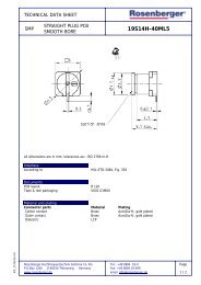
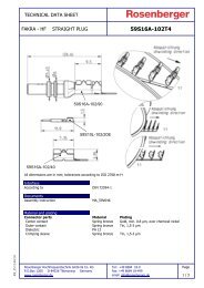
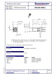
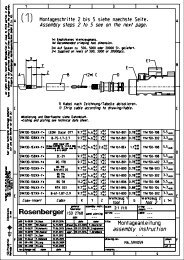
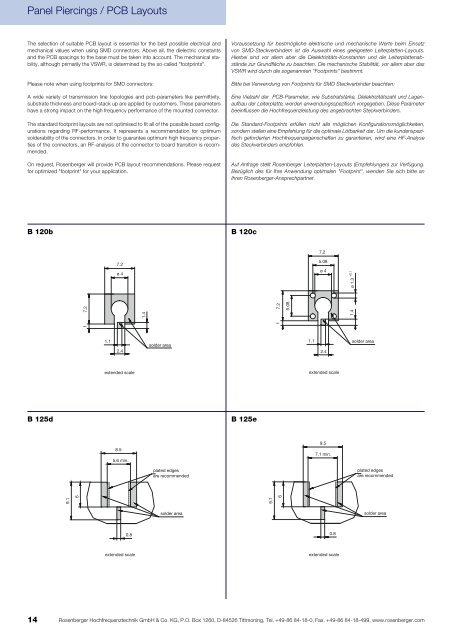
Panel Piercings / PCB Layouts<br />
3Panel Piercings / PCB Layouts<br />
The selection of suitable PCB layout is essential for the best possible electrical and<br />
mechanical values when using SMD connectors. Above all, the dielectric constants<br />
and the PCB spacings to the base must be taken into account. The mechanical stability,<br />
although primarily the VSWR, is determined by the so-called "footprints".<br />
14<br />
Voraussetzung für bestmögliche elektrische und mechanische Werte beim Einsatz<br />
von SMD-Steckverbindern ist die Auswahl eines geeigneten Leiterplatten-Layouts.<br />
Hierbei sind vor allem aber die Dielektrizitäts-Konstanten und die Leiterplattenabstände<br />
zur Grundfläche zu beachten. Die mechanische Stabilität, vor allem aber das<br />
VSWR wird durch die sogenannten "Footprints" bestimmt.<br />
Please note when using footprints for SMD connectors: Bitte bei Verwendung von Footprints für SMD Steckverbinder beachten:<br />
A wide variety of transmission line topologies and pcb-parameters like permittivity,<br />
substrate thickness and board-stack up are applied by customers. These parameters<br />
have a strong impact on the high frequency performance of the mounted connector.<br />
The standard footprint layouts are not optimised to fit all of the possible board configurations<br />
regarding RF-performance. It represents a recommendation for optimum<br />
solderability of the connectors. In order to guarantee optimum high frequency properties<br />
of the connectors, an RF-analysis of the connector to board transition is recommended.<br />
On request, <strong>Rosenberger</strong> will provide PCB layout recommendations. Please request<br />
for optimized "footprint" for your application.<br />
B 120b<br />
B 125d<br />
9.1<br />
6<br />
7.2<br />
1<br />
1.1<br />
7.2<br />
ø 4<br />
2.4<br />
extended scale<br />
8.5<br />
5.6 min.<br />
0.8<br />
extended scale<br />
1.4<br />
solder area<br />
plated edges<br />
are recommended<br />
solder area<br />
Eine Vielzahl der PCB-Parameter, wie Substratstärke, Dielektrizitätszahl und Lagenaufbau<br />
der Leiterplatte, werden anwendungsspezifisch vorgegeben. Diese Parameter<br />
beeinflussen die Hochfrequenzleistung des angebrachten Steckverbinders.<br />
Die Standard-Footprints erfüllen nicht alle möglichen Konfigurationsmöglichkeiten,<br />
sondern stellen eine Empfehlung für die optimale Lötbarkeit dar. Um die kundenspezifisch<br />
geforderten Hochfrequenzeigenschaften zu garantieren, wird eine HF-Analyse<br />
des Steckverbinders empfohlen.<br />
Auf Anfrage stellt <strong>Rosenberger</strong> Leiterplatten-Layouts (Empfehlungen) zur Verfügung.<br />
Bezüglich des für Ihre Anwendung optimalen "Footprint", wenden Sie sich bitte an<br />
Ihren <strong>Rosenberger</strong>-Ansprechpartner.<br />
B 120c<br />
B 125e<br />
solder area<br />
<strong>Rosenberger</strong> <strong>Hochfrequenztechnik</strong> GmbH & Co. KG, P.O. Box 1260, D-84526 Tittmoning, Tel. +49-86 84-18-0, Fax. +49-86 84-18-499, www.rosenberger.com<br />
7.2<br />
1<br />
9.1<br />
6<br />
5.08<br />
1.1<br />
7.2<br />
5.08<br />
ø 4<br />
2.4<br />
extended scale<br />
9.5<br />
7.1 min.<br />
0.8<br />
extended scale<br />
ø 1.3 +0.1<br />
1.4<br />
plated edges<br />
are recommended<br />
solder area