Accelerometer ACH-04-08-09 - EHAG Electronic Hardware AG
Accelerometer ACH-04-08-09 - EHAG Electronic Hardware AG
Accelerometer ACH-04-08-09 - EHAG Electronic Hardware AG

You also want an ePaper? Increase the reach of your titles
YUMPU automatically turns print PDFs into web optimized ePapers that Google loves.
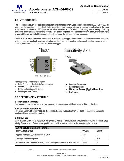
1.0 INTRODUCTION<br />
Application Specification<br />
<strong>Accelerometer</strong> <strong>ACH</strong>-<strong>04</strong>-<strong>08</strong>-<strong>09</strong> 20-07<br />
MSI P/N 1005755-1 12 OCT 00 REV B<br />
This specification covers the application requirements of Measurement Specialties <strong>Accelerometer</strong> <strong>ACH</strong>-<strong>04</strong>-<strong>08</strong>-<strong>09</strong>. The<br />
accelerometer contains one mass loaded piezoelectric sensing element oriented to measure acceleration in the plane<br />
of the device. An internal JFET provides for a low impedance, buffered output allowing a wide variety of off chip<br />
application specific signal conditioning circuitry. The sensor responds over a broad frequency range, from below 0.5Hz<br />
to above 2kHz, as a result of the integrated electronics and the damped sensing elements.<br />
The <strong>ACH</strong>-<strong>04</strong>-<strong>08</strong>-<strong>09</strong> accelerometer can be used in a wide range of applications including motion measurement and control<br />
systems, speaker feedback systems, vibration switches, shipment monitor and material handling systems, security<br />
systems, computer input/output devices, and data loggers.<br />
Features of the accelerometer include<br />
• Fully Contained Single Axis <strong>Accelerometer</strong><br />
• Low Frequency Response<br />
• Single Buffered Analog Output<br />
• Low-Impedance Output<br />
2.0 REFERENCE MATERIALS<br />
• Low Q at Resonance<br />
• Excellent Linearity<br />
• Ultra-Low Power (Typical IQ of 4µA)<br />
• Low Cost<br />
2.1 Revision Summary<br />
This paragraph is reserved for a revision summary of changes and additions made to this specification.<br />
2.2 Customer Assistance<br />
Reference MSI Part Number 1005755-1 and call (610) 650-1500 in the USA or +49 6074 862 822 in Europe to<br />
obtain additional product information.<br />
2.3 Drawings<br />
MSI Customer Drawings are available for specific products. The information contained in Customer Drawings takes<br />
priority if there is a conflict with this specification or with any other technical document supplied by MSI.<br />
2.4 Absolute Maximum Ratings<br />
CHARACTERISTICS VALUE UNITS<br />
Applied Voltage (VDD with respect to GND) +28 V<br />
Package Power Dissipation 35 MW<br />
ESD (Mil-Std-883, Method 3015.6) (qualification performed on <strong>ACH</strong><strong>04</strong>-<strong>08</strong>-05) 2000 V<br />
Rev B Measurement Specialties Incorporated, 1 of 7<br />
Printed in U.S.A.<br />
Specifications subject to change. Consult MSI for latest specifications.<br />
ER: 1005864-1
2.5 Pin Descriptions<br />
<strong>Accelerometer</strong> <strong>ACH</strong>-<strong>04</strong>-<strong>08</strong>-<strong>09</strong> 20-07<br />
MSI P/N 1005755-1<br />
PIN NUMBER NAME DESCRIPTION<br />
1 D/S1-Y � Y-Axis JFET Drain or Source<br />
2 D/S2-Y � Y-Axis JFET Source or Drain<br />
4 SGND Sensor Common<br />
8 GND Connect to GND - Device Shield<br />
14 RGND-Y Resistor GND for the Y-Axis<br />
3, 5, 6, 7, 9,<br />
10, 11, 12, 13 CTG Connect to GND<br />
�==JFET is symmetrical. The DRAIN and SOURCE are interchangeable.<br />
2.6 Environmental Characteristics<br />
CHARACTERISTICS (T=25°C) SYMBOL MIN TYP MAX UNITS<br />
Operating Temperature � TOP -40 - +85 °C<br />
Storage Temperature TS -40 - +90 °C<br />
Relative Humidity γ RH 0 - 95 %R.H.<br />
Maximum Shock (Any Axis) SMAX 1,000 - - g<br />
� Nominal sensitivity will typically change less than ±2dB over temperature range. γ Humidity must be non-condensing.<br />
2.7 Specification<br />
CHARACTERISTIC (T=25°C) „ SYMBOL MIN TYP MAX UNITS<br />
Y Axis Sensitivity � � MX 5.00 6.00 10.00 mV/g<br />
Lower Frequency Limit (3dB Point) fL3dB 0.07 0.18 0.40 Hz<br />
Upper Frequency Limit (3dB Point) fU3dB 1,000 1,500<br />
-<br />
Hz<br />
Resonant Frequency fo - 3,450 - Hz<br />
Resonant Q QR - 10 - Hz/Hz<br />
Transverse Sensitivity MT - < 20 - %<br />
Base Strain Sensitivity - - 0.03 - g/µε<br />
Temperature Transient Sensitivity - - 0.3 - g/°C<br />
Dynamic Range - - ±40 - g's<br />
Linearity (FS) - - < 0.1 < 2.0 %<br />
Equivalent Noise (100Hz) e100 - 1.0 - mg/√Hz<br />
Weight - - 0.33 - Grams<br />
„ Reference Frequency is 100 Hz. � Assumes constant current bias, guarded Drain & Source<br />
� Tighter sensitivity tolerances available. Consult factory for options.<br />
Rev B Measurement Specialties Incorporated, 2 of 7<br />
Printed in U.S.A.<br />
Specifications subject to change. Consult MSI for latest specifications.<br />
ER: 1005864-1
<strong>Accelerometer</strong> <strong>ACH</strong>-<strong>04</strong>-<strong>08</strong>-<strong>09</strong> 20-07<br />
MSI P/N 1005755-1<br />
2.8 Electrical Specifications<br />
CHARACTERISTICS (T=25°C) „ SYMBOL MIN TYP MAX UNITS<br />
Quiescent Current IQ 1 2 9 µA<br />
Gate-Drain Voltage - -30 - - V<br />
Gate-Source Voltage - -30 - - V<br />
Gate-Source Cut-Off Voltage VGS(OFF) -0.45 - 3.2 V<br />
Saturation Drain Current � IDSS 10 - 150 µA<br />
CS Forward Transconductance � gFS 50 - 210 µS<br />
„ JFET's similar to 2N4117. � Specifications modified from standard 2N4117 JFET's.<br />
Rev B Measurement Specialties Incorporated 3 of 7<br />
Printed in U.S.A.<br />
Specifications subject to change. Consult MSI for latest specifications.<br />
ER: 1005864-1
<strong>Accelerometer</strong> <strong>ACH</strong>-<strong>04</strong>-<strong>08</strong>-<strong>09</strong> 20-07<br />
MSI P/N 1005755-1<br />
2.9.1 Equivalent Electrical Schematic<br />
2.9.2 Interface Test Circuit<br />
3.0 REQUIREMENTS<br />
Notes: 1. JFET similar to 2N4117<br />
2. Conductive case connected to GND<br />
Notes: 1. Resistor value can be adjusted for individual<br />
applications.<br />
2. +/- supply voltage can be scaled<br />
3.1 Detailed Description<br />
The sensing element is a small cantilever beam consisting of a metal<br />
substrate with a piezoelectric ceramic element affixed to one side. The<br />
beam is supported at one end while the opposite end is allowed to flex in<br />
response to acceleration. A small metallic mass is bonded to the free end<br />
of the beam. The beam flex strains the piezoelectric material, which in turn<br />
generates a charge proportional to the applied acceleration. The beam is<br />
oriented to sense acceleration in the defined Y-axis.<br />
Rev B Measurement Specialties Incorporated, 4 of 7<br />
Printed in U.S.A.<br />
Specifications subject to change. Consult MSI for latest specifications.<br />
ER: 1005864-1
<strong>Accelerometer</strong> <strong>ACH</strong>-<strong>04</strong>-<strong>08</strong>-<strong>09</strong> 20-07<br />
MSI P/N 1005755-1<br />
3.2 Electrical Interface<br />
The <strong>ACH</strong>-<strong>04</strong>-<strong>08</strong>-<strong>09</strong> contains one JFET which functions as an impedance converter easing electrical interface<br />
requirements. The JFET is similar to the industry standard part number 2N4117. The user MUST bias the JFET properly<br />
in order for the unit to meet the specifications contained in this document. There are many possible interface circuits.<br />
The JFET biasing circuit, equivalent to the circuit used in MSI’s final production test, is shown on page 4. As a simple<br />
single sided source follower, the VDD can be between 3 and 28 Volts. Another example circuit is shown below.<br />
The constant-current bias circuit minimizes device-todevice<br />
and temperature related JFET transconductance<br />
variations while keeping the JFET gain near one . With the<br />
additional operational amplifier, the circuit has a gain of<br />
x148, a one-pole low-pass filter at 159Hz, and a one-pole<br />
high-pass filter at 0.34Hz. The circuit component values<br />
and DC reference/supply voltages can be scaled to fit many<br />
applications.<br />
The resistor bias circuit positions the operating point in the<br />
middle of the transconductance curve again minimizing<br />
transconductance variations. This circuit can also be<br />
powered from a single-supply voltage by creating an<br />
artificial ground, VREF.<br />
3.3 Sensitivity Variation versus Temperature<br />
The <strong>ACH</strong>-<strong>04</strong>-<strong>08</strong>-<strong>09</strong>'s typical sensitivity variation versus<br />
temperature is shown below. As shown, the sensor<br />
typical output varies +5% / -7.5% from -40 o C to +90 o C,<br />
respectively, relative to 25 o C. For many applications, this<br />
variation is acceptable (less than ±2dB from -40 o C to<br />
+90 o C). If a tighter tolerance is required, the <strong>ACH</strong>-<strong>04</strong>-<strong>08</strong>-<br />
<strong>09</strong> can be temperature compensated. A simple method<br />
is to use linear temperature coefficient resistors in the<br />
feedback network of an operational amplifier used to<br />
condition the accelerometer’s signal. KOA Speer<br />
<strong>Electronic</strong>s, Inc. (Bradford, PA) manufactures a variety of<br />
these resistors (LT73 and MLT product family). Note that<br />
since the resistors have a negative temperature<br />
coefficient, they need to be placed in the circuit such that<br />
the gain increases with increasing temperature.<br />
3.4 Temperature Transient Sensitivity (TTS)<br />
Because of the its very low operating frequency, the <strong>ACH</strong>-<strong>04</strong>-<strong>08</strong>-<strong>09</strong> exhibits high Temperature Transient Sensitivity<br />
(TTS). TTS is defined as the accelerometer’s output response to RAPID temperature changes and is expressed in<br />
equivalent g's per degree C. This effect should not be confused with the <strong>ACH</strong>-<strong>04</strong>-<strong>08</strong>-<strong>09</strong>'s sensitivity shift versus<br />
temperature which is defined at static (unchanging) temperatures and is unrelated to TTS (see above). The <strong>ACH</strong>-<strong>04</strong>-<strong>08</strong>-<br />
<strong>09</strong>'s TTS will manifest itself as a low frequency drift when the device is subjected to temperature gradients. Even small<br />
temperature changes can produce significant drift.<br />
Rev B Measurement Specialties Incorporated, 5 of 7<br />
Printed in U.S.A.<br />
Specifications subject to change. Consult MSI for latest specifications.<br />
ER: 1005864-1
<strong>Accelerometer</strong> <strong>ACH</strong>-<strong>04</strong>-<strong>08</strong>-<strong>09</strong> 20-07<br />
MSI P/N 1005755-1<br />
TTS results primarily from differences in the thermal coefficients of expansion (TCE) of the various materials in the<br />
accelerometer. During product development, every effort is made to match TCE’s. However, many mismatches are<br />
unavoidable. Even small TCE mismatches can lead to high TTS when combined with low frequency measurement<br />
capability since TTS is primarily a low frequency phenomena.<br />
Fortunately, it is easy to minimize TTS effects. The key is to<br />
prevent air currents from circulating around the <strong>ACH</strong>-<strong>04</strong>-<strong>08</strong>-<strong>09</strong>.<br />
Encasing the accelerometer in an air current shield can minimize<br />
these air currents. The shield can be made of almost anything.<br />
Successful TTS minimization shells have been made from plastic,<br />
paper, metal, etc. While the shield does not have to be airtight,<br />
tighter seals provide better performance. Encapsulating the <strong>ACH</strong>-<br />
<strong>04</strong>-<strong>08</strong>-<strong>09</strong> can also provide an effective air current shield. To ensure<br />
that the <strong>ACH</strong>-<strong>04</strong>-<strong>08</strong>-<strong>09</strong>'s housing is not compressed under the<br />
weight of the encapsulant, MSI recommends that a spacer be<br />
placed above the unit. Note that the best performance is obtained<br />
by combining an air current shield with encapsulation.<br />
3.5 Base Strain Sensitivity (BSS)<br />
The <strong>ACH</strong>-<strong>04</strong>-<strong>08</strong>-<strong>09</strong> displays Base Strain Sensitivity (BSS) for many<br />
of the same reasons that it displays TTS; namely, low frequency operation and low modulus/high TCE materials. BSS<br />
is defined as the amount of output signal generated as a result of strain in the accelerometer’s mounting surface and is<br />
expressed in terms of equivalent g's per base micro-strain, g/µε.<br />
The best way to minimize BSS effects is to stiffen the mounting structure. Stiffer mounting structures are typically less<br />
susceptible to bending. However, since the <strong>ACH</strong>-<strong>04</strong>-<strong>08</strong>-<strong>09</strong> is designed to be attached to a circuit board, it may be<br />
impractical to stiffen the mounting surface.<br />
In this situation, the accelerometer can be mounted at the end of a<br />
cantilever beam routed into the circuit board, where minimal strain is coupled<br />
into the accelerometer. Mounting arrangements such as this are very<br />
effective for low frequency applications. However, they are unacceptable for<br />
high frequency measurements where the signal to be measured is near or<br />
above the resonant frequency of the circuit board's cantilever beam.<br />
Implementation of a cantilever beam, strain minimization design requires<br />
careful analysis to accurately position the cantilever resonance well above<br />
the frequency range of interest.<br />
Air Current Shield<br />
Air Current Shield<br />
& Encapsulation<br />
3.6 IC Package<br />
To insure proper protection against RF and EM interference, the outer surface of the package is conductive and<br />
electrically connected to the GND pin. Exercise caution when laying out PC boards to ensure that no uninsulated traces<br />
are located under the package. They could contact the package surface and be shorted to GND. It is recommended<br />
that all 14 pins of the package be soldered to the PC board to insure good mechanical coupling of acceleration, motion,<br />
and shock. Complete soldering will also eliminate undesirable mechanical resonances of the IC package.<br />
Rev B Measurement Specialties Incorporated, 6 of 7<br />
Printed in U.S.A.<br />
Specifications subject to change. Consult MSI for latest specifications.<br />
ER: 1005864-1
<strong>Accelerometer</strong> <strong>ACH</strong>-<strong>04</strong>-<strong>08</strong>-<strong>09</strong> 20-07<br />
MSI P/N 1005755-1<br />
The package is sealed to eliminate the effects of normal exposure to the environment and typical cleaning processes<br />
found in an electronic manufacturing facility. However, the package seal is not hermetic and exposure to acidic, basic,<br />
corrosive, or aqueous environments is not recommended. Because of process variations, the <strong>ACH</strong>-<strong>04</strong>-<strong>08</strong>-<strong>09</strong> should be<br />
qualified through the intended production assembly processes (soldering, wash, etc.) before releasing to production.<br />
Recommended alternative soldering processes include laser, hand and hot bar soldering. Contact MSI for more detailed<br />
information.<br />
3.7 <strong>ACH</strong>-<strong>04</strong>-<strong>08</strong>-<strong>09</strong> Mechanical Dimensions<br />
Rev B Measurement Specialties Incorporated, 7 of 7<br />
Printed in U.S.A.<br />
Specifications subject to change. Consult MSI for latest specifications.<br />
ER: 1005864-1