DSCC 03029 - Kemet
DSCC 03029 - Kemet
DSCC 03029 - Kemet
- TAGS
- dscc
- kemet
- www.kemet.com

You also want an ePaper? Increase the reach of your titles
YUMPU automatically turns print PDFs into web optimized ePapers that Google loves.
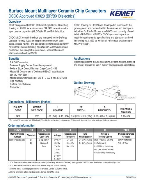
Surface Mount Multilayer Ceramic Chip Capacitors<br />
<strong>DSCC</strong> Approved <strong>03029</strong> (BR/BX Dielectrics)<br />
Overview<br />
KEMET is approved to <strong>DSCC</strong> (Defense Supply Center, Columbus)<br />
drawing no. <strong>03029</strong> for surface mount EIA 0402 case size multilayer<br />
ceramic capacitors (MLCCs) in BR and BX dielectrics.<br />
<strong>DSCC</strong> MLCC control drawings are managed by the Defense<br />
Logistics Agency (DLA) and represent devices with case<br />
sizes, voltage ratings, and capacitance offerings not currently<br />
referenced in a valid military specifi cation. Approved devices<br />
must meet the stringent requirements, specifi cations and<br />
standards outlined by <strong>DSCC</strong>.<br />
Benefi ts<br />
• EIA 0402 case size<br />
• Defense Supply Center, Columbus approved<br />
• Federal Stock Control Number, Cage Code 31433<br />
• Meets US Department of Defense (USDoD) specifi cations<br />
per MIL-PRF-55681<br />
• Meets USDoD standards per MIL-STD 202 & MIL-STD-1285<br />
• High reliability<br />
• Surface mount device<br />
• Non-polar<br />
Dimensions - Millimeters (Inches)<br />
EIA SIZE<br />
CODE<br />
METRIC<br />
SIZE CODE<br />
L<br />
LENGTH^<br />
<strong>DSCC</strong> drawing no. <strong>03029</strong> was developed in response to the<br />
growing need and demand within the defense and aerospace<br />
industries for EIA 0402 case size MLCCs not currently offered<br />
in MIL-PRF-55681. KEMET’s <strong>DSCC</strong> approved capacitors<br />
meet the requirements, specifi cations and standards outlined<br />
in drawing no. <strong>03029</strong> as well as all referenced provisions per<br />
MIL-PRF-55681.<br />
Applications<br />
Typical applications include decoupling, bypass, fi ltering, blocking<br />
and energy storage for use in military and aerospace applications.<br />
Outline Drawing<br />
W<br />
WIDTH^<br />
B<br />
BANDWIDTH<br />
T<br />
THICKNESS<br />
Maximum<br />
0402 1005 1.02 (.040) ± 0.10 (.004) 0.51 (.020) ± 0.10 (.004) 0.25 (.010) ± 0.15 (.006) 0.61 (.024)<br />
^For symbol “U” termination add .20 inches (0.51mm) to the positive length tolerance and .015 inches (0.38mm) to the positive width and thickness tolerances.<br />
© KEMET Electronics Corporation • P.O. Box 5928 • Greenville, SC 29606 (864) 963-6300 • www.kemet.com F4003 06/10<br />
B<br />
70Sn/30Pb<br />
Nickel N Plate<br />
Conductive C Metallization<br />
Electrodes<br />
Ordering Information<br />
<strong>03029</strong> BX 222 Z J Z C 7189<br />
<strong>DSCC</strong> Drawing<br />
Number<br />
Dielectric<br />
Capacitance<br />
Code (pF)<br />
Voltage<br />
Capacitance<br />
Tolerance<br />
End<br />
Metallization^<br />
Group C<br />
Testing Option<br />
Packaging/Grade<br />
(C-Spec)*<br />
<strong>03029</strong> (0402 case size) BR 2 Sig. Digits + W = 6.3V J = ±5% U = SnPb (4%min) Blank = No group C testing Blank = Waffl e Pack<br />
BX Number of X = 10V K = ±10% Z = SnPb (4%min) C = Full group C 7189 = 7” Reel<br />
Zeros Y = 16V M = ±20% L = 2,000 hour life test only<br />
Z = 25V M = 1,000 hour life test only<br />
A = 50V<br />
B = 100V<br />
C = 200V<br />
H = Low voltage humidity only<br />
^ “U” = Base metallization-barrier metal-solder coated (tin/lead alloy, with a min of 4% lead). Melting point is +200ºC or less. Metallization thickness is ≥ 60μ-inches.<br />
^ “Z” = Base metallization-barrier metal-tinned (tin/lead alloy, with a min of 4% lead).<br />
* Additional reeling or packaging options may be available. Contact KEMET for details.<br />
Additional termination options may be available. Contact KEMET for details.
<strong>DSCC</strong> Approved <strong>03029</strong> (BR/BX Dielectrics)<br />
Electrical Parameters/Characteristics: BR Dielectric<br />
Operating Temperature Range -55°C to +125°C<br />
Capacitance Change with Reference to +25°C and 0 Vdc Applied: ±15%<br />
Capacitance Change with Reference to +25°C and 100% Rated Vdc Applied: +15%, -40%<br />
Aging Rate (Max % Cap Loss/Decade Hour) 1%<br />
Dielectric Withstanding Voltage 250%<br />
Dissipation Factor (DF%) Maximum Limits @ 25ºC 5% (10V), 3.5% (16V & 25V) and 2.5% (50V to 200V)<br />
Insulation Resistance (IR) Limit @ 25°C 1000 megohm microfarads (minimum) or 100GΩ<br />
Insulation Resistance (IR) Limit @ 125°C 100 megohm microfarads (minimum) or 10GΩ<br />
To obtain the IR limit, divide MΩ-μF value by the capacitance and compare to GΩ limit. Select the lower of the two limits.<br />
Capacitance and Dissipation Factor (DF) measured under the following conditions:<br />
1kHz ± 50Hz and 1.0 ± 0.2 Vrms if capacitance >1000pF<br />
Electrical Parameters/Characteristics: BX Dielectric<br />
Operating Temperature Range -55°C to +125°C<br />
Capacitance Change with Reference to +25°C and 0 Vdc Applied: ±15%<br />
Capacitance Change with Reference to +25°C and 100% Rated Vdc Applied: +15%, -25%<br />
Aging Rate (Max % Cap Loss/Decade Hour) 1%<br />
Dielectric Withstanding Voltage 250%<br />
Dissipation Factor (DF%) Maximum Limits @ 25ºC 5% (10V), 3.5% (16V & 25V) and 2.5% (50V to 200V)<br />
Insulation Resistance (IR) Limit @ 25°C 1000 megohm microfarads (minimum) or 100GΩ<br />
Insulation Resistance (IR) Limit @ 125°C 100 megohm microfarads (minimum) or 10GΩ<br />
To obtain the IR limit, divide MΩ-μF value by the capacitance and compare to GΩ limit. Select the lower of the two limits.<br />
Capacitance and Dissipation Factor (DF) measured under the following conditions:<br />
1kHz ± 50Hz and 1.0 ± 0.2 Vrms if capacitance >1000pF<br />
Qualifi cation/Certifi cation<br />
Qualifi cation Inspection per MIL-PRF-55681<br />
Inspection Test method paragraph<br />
Group I<br />
Voltage conditioning 4.8.3<br />
DWV 4.8.9<br />
IR (elevated temperature) 4.8.6<br />
Capacitance 4.8.4<br />
Dissipation factor 4.8.5<br />
IR 4.8.6<br />
DWV 4.8.9<br />
Visual and mechanical examination 4.8.2<br />
Group II<br />
Solderability 4.8.10<br />
Group III<br />
Voltage-temperature limits 4.8.11<br />
Thermal shock and immersion 4.8.12<br />
Group IV<br />
Resistance to soldering heat 4.8.13<br />
Moisture resistance 4.8.14<br />
Group V<br />
Life (at elevated ambient temperature) 4.8.16<br />
Group VIII<br />
Humidity, steady state, low voltage 4.8.15<br />
© KEMET Electronics Corporation • P.O. Box 5928 • Greenville, SC 29606 (864) 963-6300 • www.kemet.com F4003 06/10
<strong>DSCC</strong> Approved <strong>03029</strong> (BR/BX Dielectrics)<br />
Electrical Characteristics<br />
Magnitude Ohms<br />
Magnitude Ohms<br />
10 4<br />
10 3<br />
10 2<br />
10 1<br />
10 0<br />
10 -1<br />
10 -2<br />
10 4<br />
10 3<br />
10 2<br />
10 1<br />
10 0<br />
10 -1<br />
10 -2<br />
10 4<br />
10 4<br />
Z & ESR - 0402, 1000pF, 25V, BX<br />
10 5<br />
10 5<br />
10 6<br />
10 6<br />
10 7<br />
Freq (Hz)<br />
10 7<br />
Freq (Hz)<br />
10 8<br />
10 8<br />
10 9<br />
10 9<br />
ESR<br />
Z<br />
ESR<br />
Z<br />
10 10<br />
10 10<br />
© KEMET Electronics Corporation • P.O. Box 5928 • Greenville, SC 29606 (864) 963-6300 • www.kemet.com F4003 06/10<br />
ΔC/C (%)<br />
ΔC/C (%)<br />
10<br />
0<br />
-10<br />
-20<br />
-30<br />
-40<br />
10<br />
0<br />
-10<br />
-20<br />
-30<br />
-40<br />
TCVC - 0402, 1000pF, 25V, BX<br />
-55 -35 -15 5 25 45 65 85 105 125<br />
Temperature (°C)<br />
Z & ESR - 0402, 2200pF, 50V, BR TCVC - 0402, 2200pF, 50V, BR<br />
-55 -35 -15 5 25 45 65 85 105 125<br />
Temperature (°C)<br />
0 VDC<br />
25 VDC<br />
0 VDC<br />
50 VDC
<strong>DSCC</strong> Approved <strong>03029</strong> (BR/BX Dielectrics)<br />
Capacitance<br />
pF<br />
Cap<br />
Code<br />
Packaging Quantities<br />
DIELECTRIC<br />
<strong>DSCC</strong> DRAWING NO. <strong>03029</strong><br />
BR BX<br />
Voltage<br />
Soldering Process<br />
All parts incorporate the standard KEMET barrier layer of pure nickel with a tin-lead (SnPb) fi nish. Both “U” and “Z” termination fi nishes<br />
contain a minimum of 4% lead.<br />
Marking<br />
Marking is not available for EIA 0402 case size capacitors. These chips will be supplied unmarked.<br />
6.3V<br />
10V<br />
16V<br />
© KEMET Electronics Corporation • P.O. Box 5928 • Greenville, SC 29606 (864) 963-6300 • www.kemet.com F4003 06/10<br />
25V<br />
50V<br />
100V<br />
Voltage Code W X Y Z A B C W X Y Z A B C<br />
Cap Tolerance EIA 0402 CASE SIZE<br />
100 101 J K M • • • • • • • • • •<br />
120 121 J K M • • • • • • • • • •<br />
150 151 J K M • • • • • • • • • •<br />
180 181 J K M • • • • • • • • • •<br />
220 221 J K M • • • • • • • • • •<br />
270 271 J K M • • • • • • • • • •<br />
330 331 J K M • • • • • • • • • •<br />
390 391 J K M • • • • • • • • • •<br />
470 471 J K M • • • • • • • • • •<br />
560 561 J K M • • • • • • • • • •<br />
680 681 J K M • • • • • • • • • •<br />
820 821 J K M • • • • • • • • • •<br />
1,000 102 J K M • • • • • • • • • •<br />
1,200 122 J K M • • • • • • • • •<br />
1,500 152 J K M • • • • • • • • •<br />
1,800 182 J K M • • • • • • • • •<br />
2,200 222 J K M • • • • • • • • •<br />
2,700 272 J K M<br />
3,300 332 J K M<br />
3,900 392 J K M<br />
4,700 472 J K M<br />
5,600 562 J K M<br />
6,800 682 J K M<br />
8,200 822 J K M<br />
10,000 103 J K M<br />
12,000 123 J K M<br />
CHIP SIZE (EIA) TAPE SIZE<br />
BULK QUANTITY<br />
WAFFLE PACKAGING (Default)<br />
7” REEL QUANTITY<br />
PAPER TAPE<br />
0402 8mm 100 10,000<br />
Please refer to the “Ordering Information” section of this document for packaging ordering information.<br />
200V<br />
6.3V<br />
10V<br />
16V<br />
25V<br />
50V<br />
100V<br />
200V