

icepower1000adata
icepower1000adata
icepower1000adata

Create successful ePaper yourself
Turn your PDF publications into a flip-book with our unique Google optimized e-Paper software.
Bang & Olufsen ICEpower a/s, Gl. Lundtoftevej 1b, DK-2800 Kgs. Lyngby<br />
Phone [45] 45 20 36 00, Fax [45] 45 20 36 99, CVR-no. 25053591<br />
ICEpowerinfo@bang-olufsen.dk, www.icepower.bang-olufsen.com<br />
ICEpower1000A<br />
1000W General Purpose ICEpower Amplifier<br />
Version 2.1<br />
Contents<br />
General Description ......................................................................................... 2<br />
Block Diagram ................................................................................................. 3<br />
Connection Diagram........................................................................................ 3<br />
Absolute Maximum Ratings ............................................................................. 5<br />
Electrical Specifications .................................................................................... 5<br />
Timing Specifications ....................................................................................... 6<br />
Typical Performance Characteristics ................................................................. 6<br />
Application Information................................................................................... 9<br />
Operational Timing Diagram.......................................................................... 11<br />
Features......................................................................................................... 12<br />
Thermal Design.............................................................................................. 14<br />
Power Supply................................................................................................. 14<br />
Physical Dimensions ....................................................................................... 15<br />
Notice............................................................................................................ 16<br />
1/16
ICEpower1000A, 1000W General Purpose Amplifier Version 2.1<br />
General Description<br />
The ICEpower1000A is a general purpose amplifier solution. By<br />
using patented, state-of-the-art ICEpower ® analogue technology,<br />
the ICEpower1000A achieves extremely high fidelity in a compact<br />
package.<br />
The 3 kHz bandwidth and the ability to operate from a variety of<br />
power sources means the ICEpower1000A can be used in:<br />
• Active speakers and subwoofers<br />
• A/V amplifiers/receivers<br />
• Automotive amplifiers<br />
• Musical instrument amplifiers<br />
• Marine audio products<br />
• Installation audio products<br />
2/16<br />
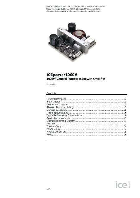
Figure 1: ICEpower1000A<br />
Size: 10 x 10 x 2.7cm<br />
True high-end performance is guaranteed by the patented, proprietary COM modulation and MECC control<br />
techniques and the integrated, turn-key design reduces design-in cost and shortens Time-to-Market for the end<br />
product.<br />
Key Specifications<br />
• 1000W @ 0.04% THD+N, 100Hz, 4Ω.<br />
• Peak output current > 50A.<br />
• 120dBA dynamic range.<br />
• THD = 0.008% @ 100Hz, 1W<br />
• THD+N < 0.1%, 0.1W – 1000W, 4Ω.<br />
• Efficiency = 93% @ 500W, 8Ω.<br />
• Output impedance < 5mΩ @ 1kHz.<br />
• Power Supply Rejection Ratio > 60dB.<br />
• Output DC offset < 40mV.<br />
Key Features<br />
• Very rugged design for demanding use<br />
• Soft mute/de-mute<br />
• Stand-by mode for low power consumption<br />
• Under voltage protection<br />
• Monitor output<br />
• Balanced input and output<br />
• Excellent EMI performance<br />
• No heat sink required
ICEpower1000A, 1000W General Purpose Amplifier Version 2.1<br />
Block Diagram<br />
3/16<br />
Vi+<br />
Vi-<br />
Mute<br />
Vcc<br />
Standby<br />
Vss<br />
AGND<br />
Connection Diagram<br />
Input filter<br />
DC blocking<br />
Control/<br />
Protection<br />
Disable<br />
Soft clipping<br />
Mute<br />
ICEpower®<br />
COM Pulse Modulation<br />
MECC Error Correction and Control<br />
Figure 2: ICEpower1000A block diagram.<br />
Figure 3: ICEpower1000A-IC connections.<br />
Power Conversion<br />
Stage<br />
with Demodulation<br />
The plug interface of the ICEpower1000A has two industry standard connectors that have been selected for<br />
long-term reliability. The power AMP FAST-ON 928 492-4 connector is used for power input and speaker output.<br />
The JST PH-connector is used for low level power supply, audio input and the control features.<br />
Monitor<br />
Vp<br />
Vo+<br />
Vo-<br />
PGND
ICEpower1000A, 1000W General Purpose Amplifier Version 2.1<br />
Power Connector Specification<br />
Pin Function Description<br />
1 Vo- “Cold” balanced power output terminals. In phase with Vi -<br />
2 Vo+ “Hot“ balanced power output terminals. In phase with Vi+<br />
3 PGND Power GND for the single ended power supply input Vp.<br />
4 Vp Power Supply (single) for the power stage<br />
Table 1: Power Connector Specification.<br />
Signal Connector Specification<br />
ICEpower* Function Description JST**<br />
Pin numbering<br />
Pin numbering<br />
1 Vcc Positive power supply input for the signal section. 8<br />
2 Vss Negative power supply input for the signal section. 7<br />
3 AGND Ground terminal for the signal section. 6<br />
4 Monitor Unbalanced attenuated output signal. 5<br />
5 Vi+ Positive input (balanced input buffer). 4<br />
6 Vi- Negative input (balanced input buffer). 3<br />
7 Mute Mute input (Internal pull-up). 2<br />
4/16<br />
8 Standby Control pin for standby control. (Internal pull-up).<br />
* This pin numbering is used by ICEpower in all ICEpower documentation<br />
**This pin numbering is used by JST- JST is the manufacturer of the PHR-08 connector.<br />
Table 2: Signal Connector Specification.<br />
1
ICEpower1000A, 1000W General Purpose Amplifier Version 2.1<br />
Absolute Maximum Ratings<br />
Absolute maximum ratings indicate limits beyond which damage may occur.<br />
Symbol Parameter Value Unit<br />
Vp Operating power supply level 135 V<br />
Vcc Positive analog supply 15 V<br />
Vss Negative analog supply –15 V<br />
Vin Maximum differential input voltage ±12 V<br />
Tcase Maximum case temperature 90<br />
O C<br />
Rth,case-rib Thermal resistance, case–rib 2 K/W<br />
CL Maximum capacitive loading 470 nF<br />
Ta Maximum operating ambient temperature 60<br />
Table 3: Absolute Maximum ratings.<br />
Electrical Specifications<br />
Unless otherwise specified, f=1kHz, PO =1W, Ta = 25 O C.<br />
Symbol Parameter Conditions Min Typ Max Unit<br />
Vp Power Supply Operation 40 120 125 V<br />
Vcc Positive analog supply Operation 10 12 15 V<br />
Vss Negative analog supply Operation -10 -12 -15 V<br />
PO<br />
Output power @ 0.1%THD+N<br />
10Hz < f < 1kHz<br />
(AES17 measurement filter) 2)<br />
RL=4Ω, Vp =120V<br />
RL=6Ω, Vp =120V<br />
RL=8Ω, Vp =120V<br />
1000<br />
800<br />
600<br />
W<br />
THD+N THD+N in 4Ω<br />
(AES17 measurement filter) 2)<br />
f = 100Hz, PO =1W 0.008 0.01 %<br />
THD+N Maximal THD+N in 4Ω<br />
(AES17 measurement filter) 2)<br />
10Hz < f < 1kHz<br />
0.05 0.07 %<br />
100mW < Po < 100W<br />
IVp Quiescent current Vp = 120V 20 35 40 mA<br />
Ivp_standby Standby current Vp = 120V 1 mA<br />
IVcc Quiescent current Vcc = 12V 200 230 mA<br />
IVcc_standby Standby current Vcc = 12V 35 mA<br />
IVss Quiescent current Vss = -12V 25 mA<br />
IVss_Standby Standby current Vss = -12V 25 mA<br />
fo Switching frequency Idle 270 300 350 kHz<br />
fS Switching frequency range Idle to full scale variation 50 300 350 kHz<br />
η Power Stage Efficiency RL = 8Ω, PO =500W 93 %<br />
PSRR Power Supply Rejection Ratio Voltage ripple @<br />
60 dB<br />
of Vp<br />
f = 100 – 120 Hz<br />
VN, O Output referenced idle noise A-weighted<br />
10Hz < f < 20kHz<br />
70 80 100 μV<br />
VOFF, Diff Differential offset on output<br />
terminals<br />
Input terminated. ±40 mV<br />
VOFF, CM<br />
5/16<br />
Common mode offset on output<br />
terminals<br />
Input terminated. Vp / 2 ±10% V<br />
Av Nominal Voltage Gain 1kHz 27.8 28.1 28.4 dB<br />
f Frequency response 20 – 1kHz, all loads ±0.5 ±1 dB<br />
fu Upper bandwidth limit (-3dB) RL = 4Ω 3 kHz<br />
fl<br />
Lower bandwidth limit<br />
(-3dB)<br />
RL = 4Ω<br />
O C<br />
4 Hz<br />
Zo Output impedance f = 1kHz 5 10 mΩ<br />
ZL Load impedance range 2 4 ≡ Ω<br />
D Dynamic range A-weighted 120 dB<br />
Table 4: Electrical Specifications.<br />
2) AES 17, 22 kHz 7 th order Audio Precision measurement filter is used.
ICEpower1000A, 1000W General Purpose Amplifier Version 2.1<br />
Timing Specifications<br />
Symbol Parameter Conditions Min Typ Max Unit<br />
200 250 300 ms<br />
6/16<br />
t sd Switching start up delay Time from when all power supplies<br />
3) are within operational limits<br />
t pdm Output delay Time delay to signal 3) 350 400 500 ms<br />
t md Mute delay Time delay to mute 3) 30 50 100 ms<br />
t dmd De-mute delay Time to demute 3) 300 350 400 ms<br />
t psd Shutdown delay Supply failure or Standby pin 3) 1 5 μs<br />
Table 5: Timing Specifications.<br />
3) For details see Figure 13 and 14.<br />
Typical Performance Characteristics<br />
Figure 4: Frequency response in 4Ω, 8Ω, 16Ω and open load. Top – amplitude. Bottom – phase.
ICEpower1000A, 1000W General Purpose Amplifier Version 2.1<br />
Efficiency vs. Output Power<br />
7/16<br />
100<br />
90<br />
80<br />
70<br />
60<br />
% 50<br />
40<br />
30<br />
20<br />
10<br />
0<br />
0 50 100 150 200 250<br />
Watts<br />
100<br />
90<br />
80<br />
70<br />
60<br />
% 50<br />
40<br />
30<br />
20<br />
10<br />
Figure 5: Efficiency vs. output power (16Ω).<br />
0<br />
0 100 200 300 400 500<br />
Watts<br />
100<br />
90<br />
80<br />
70<br />
60<br />
% 50<br />
40<br />
30<br />
20<br />
10<br />
Figure 6: Efficiency vs. output power (8Ω).<br />
0<br />
0 200 400 600 800 1000<br />
Watts<br />
Figure 7: Efficiency vs. output power (4Ω).
ICEpower1000A, 1000W General Purpose Amplifier Version 2.1<br />
Harmonic Distortion & Noise<br />
8/16<br />
THD+N vs. output power at 100Hz and 1kHz 4) (8Ω).<br />
THD+N vs. output power at 100Hz and 1kHz 4) (4Ω).<br />
Idle noise (16K FFT). Residual = 70μV(A).<br />
FFT Analysis. f = 1kHz/100mW 4W loading. THD = -106dB<br />
(0.0005%)<br />
f= 1kHz. Po = 1W. 4Ω loading. THD = 0.008%.<br />
Figure 8: Harmonic Distortion & Noise.<br />
4) AES 17, 22 kHz 7 th order Audio Precision measurement filter is used.
ICEpower1000A, 1000W General Purpose Amplifier Version 2.1<br />
Application Information<br />
To simplify product development, the ICEpower1000A is designed as a “complete” component electrically and<br />
mechanically. A typical ICEpower1000A component application is a single channel application (e.g. an active<br />
subwoofer system). An example is shown in Figure 9.<br />
9/16<br />
Power Supply<br />
Preamp,<br />
Filter etc.<br />
Stby / Mute control<br />
-12V<br />
+12V<br />
120V DC<br />
10000uF/150V<br />
Vi+<br />
Vi-<br />
Mute<br />
Standby<br />
AGND<br />
540uF<br />
Vp Vcc Vss<br />
Av = 28.1dB<br />
PGND<br />
22uF 22uF<br />
Figure 9: Typical application.<br />
Input/Output Interfaces<br />
The balanced input section provides signal buffering and anti-alias filtering. The balanced configuration helps to<br />
avoid hum and noise pick-up. If an unbalanced input be preferred this can be set by shorting Vi- and AGND.<br />
Figure 10: Balanced input buffer / anti-aliasing filter<br />
The anti-aliasing filter bandwidth is 100 kHz and the filter characteristics are shaped to match the power<br />
amplification section. The audio bandwidth is 3 kHz and the input impedance is approximately 8kΩ over the<br />
audio bandwidth. This presents an acceptable load for most pre-amps, active crossover outputs etc.<br />
Vo+<br />
Vo-
ICEpower1000A, 1000W General Purpose Amplifier Version 2.1<br />
Output Stage<br />
The output stage is a bridge topology with a 2 nd order filter. This leads to a balanced power output on the<br />
terminals Vo+ and Vo-. The filter design is a part of the proprietary MECC topology and has been chosen as a<br />
compromise between demodulation, efficiency and filter volume.<br />
10/16<br />
Power<br />
Stage<br />
The essential output characteristics are:<br />
ICEpower1000A<br />
L<br />
L<br />
Output filter<br />
Figure 11: Output filter section with compensating Zobel network.<br />
• The output impedance is below 25mΩ @ 6 kHz.<br />
• The output residual basically consists of a single frequency component at the carrier fundamental of<br />
approximately 300kHz. In a standard application set-up, the output characteristics lead to compliance with<br />
the EN and FCC directives on EMI.<br />
• The system bandwidth is 3 kHz with a 4Ω load.<br />
The ICEpower1000A is designed to have low output impedance at all frequencies (see Figure 4) and thus be<br />
unaffected by loading characteristics. Care should however be taken with purely capacitive loads. The<br />
ICEpower1000A is designed to be stable with purely capacitive loads up to 100nF. Higher capacitive loads may<br />
compromise stability and thus damage the device.<br />
Warning! The balanced speaker outputs are both “hot” with a common-mode DC level equal to Vp/2. Always<br />
use balanced probes for monitoring and measurements. Shorting one of the terminals to ground results in an<br />
over current situation. As the module has no internal current limiter even a brief short circuit (phase-to-phase or<br />
phase-to-GND) will damage the device beyond repair. Current limiting circuitry must be connected externally.<br />
C<br />
CZ<br />
RZ<br />
Vo+<br />
Vo-
ICEpower1000A, 1000W General Purpose Amplifier Version 2.1<br />
Operational Timing Diagram<br />
The power supply input pins, the Standby pin and the Mute pin control the ICEpower1000A. If the supplies are<br />
not above their minimum values the amplifier will enter standby mode. The amplifier can be forced into standby<br />
mode by pulling the standby pin low. The Mute pin will not stop the switching of the amplifier, but attenuates<br />
the output signal by 60dB when pulled low.<br />
11/16<br />
Mute<br />
Signal Out<br />
All power supplies good<br />
or<br />
STANDBY<br />
Switching<br />
Signal Out<br />
t md<br />
Figure 12: Mute and demute timing definitions.<br />
tsd tpdm t dmd<br />
Figure 13: Supply start-up and shut down timing definitions.<br />
Power-up Sequence<br />
The power supplies control power-up of the ICEpower1000A. When the power supplies reach operational<br />
power levels the switching output stage is enabled with a 50% duty-cycle (zero modulation). To ensure power<br />
supply stability before start-up, a propagation delay of tsd = 250ms (typical value) has been introduced. The builtin<br />
mute function subsequently releases the input signal with a timed delay of tdmd = 350ms for a soft, controlled<br />
start-up sequence. The total delay from power is applied until full signal amplification is available is thus 600ms.<br />
Power-down Sequence<br />
The module will enter standby mode if:<br />
1. One of the power supplies drops below the minimum acceptable level or falls out completely.<br />
2. The standby pin is pulled low.<br />
In either case the ICEpower1000A will shut off instantly (1μs) by muting the signal and disabling the output<br />
stage. After a power-down, meaning when the standby pin is released and/or the power supplies return to<br />
nominal values, the ICEpower1000A will power up using the standard power-up sequence as described above.<br />
t psd
ICEpower1000A, 1000W General Purpose Amplifier Version 2.1<br />
Features<br />
Mute Control<br />
The mute function has been implemented to allow soft mute/de-mute of the module. The recommended<br />
external interface circuit for this pin can be seen on Figure 14. Timing specifications are only valid with the<br />
interface shown.<br />
12/16<br />
Figure 14: Interface and simplified internal circuit for the MUTE pin.<br />
Standby Control<br />
The Standby pin can be used to put the module in a low power consumption mode. Pulling the standby pin low<br />
sets the standby mode. This function allows quick shutdown of the module and can be used for protection of<br />
the module. The recommended external circuit is shown in Figure 15. The timing specifications are only valid<br />
with the interface circuit shown.<br />
Figure 15: Interface and simplified internal circuit for STANDBY pin.
ICEpower1000A, 1000W General Purpose Amplifier Version 2.1<br />
Monitor Output<br />
The monitor output has been implemented as an attenuated, ground referenced version of the balanced output<br />
signal. The internal output circuit of this output is shown in Figure 16. The bandwidth for the monitor output is<br />
limited to 45 kHz.<br />
13/16<br />
Monitor<br />
47k 47k<br />
150p<br />
Internal Feedback<br />
-<br />
-28.3dB<br />
Figure 16: Internal circuitry of the monitor output.<br />
+<br />
Vo+ Vo-
ICEpower1000A, 1000W General Purpose Amplifier Version 2.1<br />
Thermal Design<br />
Thermal design is generally a great challenge in power amplifier systems. Linear amplifier designs operating in<br />
class A or AB are normally very inefficient and therefore equipped with extensive heat sinking to keep the<br />
transistor junction temperature low. The ICEpower1000A is based on highly efficient ICEpower switching<br />
technology providing high overall efficiency characteristics at all levels of operation. Refer to the efficiency vs.<br />
output power graph in the section “Typical performance characteristics” for more information.<br />
With Rth, case-rib = 2 K/W the heat sink can be designed using normal thermal design considerations. Mounting<br />
the ICEpower1000A to an aluminium backplane or enclosure is normally sufficient to ensure trouble-free<br />
operation even under continuous loading. Please note that the module relies on both the heat sink and the<br />
ambient air for cooling and so it must be ensured that neither Tcase nor Ta is exceeded during operation. The<br />
ICEpower1000A has no thermal shutdown feature and a suitable thermal monitoring circuit must be connected<br />
externally if the application requires protection against thermal overload.<br />
Power Supply<br />
The ICEpower1000A has excellent power supply rejection on the main supply line (Vp) due to the use of<br />
ICEpower’s patented COM modulation, and as such there are no specific requirements for power supply<br />
stabilization. The ICEpower1000A runs well even on an unstabilized supply, linear or switch-mode, with several<br />
volts of ripple. The COM modulation technology also means that power supply bypassing and layout are not<br />
critical and that poor layouts will not cause stability problems as can be the case in linear amplifier designs.<br />
The analog Vcc and Vss supply lines must be regulated. Noise and ripple on these supplies will directly affect<br />
overall system performance and voltages exceeding 15V on either line will damage the device.<br />
14/16
ICEpower1000A, 1000W General Purpose Amplifier Version 2.1<br />
Physical Dimensions<br />
15/16<br />
Figure 17: Physical Dimensions, ICEpower1000A-IC.
ICEpower1000A, 1000W General Purpose Amplifier Version 2.1<br />
Notice<br />
The data sheet contains specifications that may be subject to change without prior notice. ICEpower is a<br />
trademark of Bang & Olufsen ICEpower a/s.<br />
Bang & Olufsen ICEpower a/s products are not authorized for use as critical components in life support devices<br />
or systems without the express written approval of the president and general counsel of Bang & Olufsen<br />
ICEpower a/s. As used herein:<br />
16/16<br />
1. Life support devices or systems are devices or systems which, (a) are intended for surgical implant into<br />
the body, or (b) support or sustain life, and whose failure to perform when properly used in accordance<br />
with instructions for use provided in the labeling, can be reasonably expected to result in a significant<br />
injury to the user.<br />
2. A critical component is any component of a life support device or system whose failure to perform can<br />
be reasonably expected to cause the failure of the life support device or system, or to affect its safety or<br />
effectiveness.