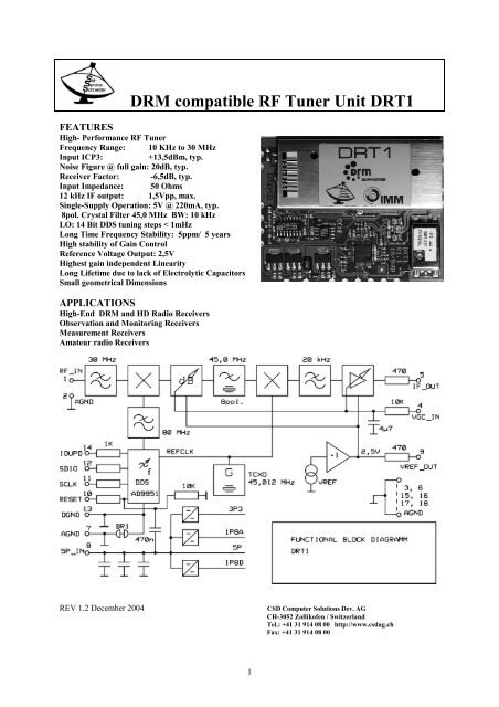
DRM compatible RF Tuner Unit DRT1 - CSD Computer Solutions ...
DRM compatible RF Tuner Unit DRT1 - CSD Computer Solutions ...
DRM compatible RF Tuner Unit DRT1 - CSD Computer Solutions ...

You also want an ePaper? Increase the reach of your titles
YUMPU automatically turns print PDFs into web optimized ePapers that Google loves.
<strong>DRM</strong> <strong>compatible</strong> <strong>RF</strong> <strong>Tuner</strong> <strong>Unit</strong> <strong>DRT1</strong><br />
FEATURES<br />
High- Performance <strong>RF</strong> <strong>Tuner</strong><br />
Frequency Range: 10 KHz to 30 MHz<br />
Input ICP3: +13,5dBm, typ.<br />
Noise Figure @ full gain: 20dB, typ.<br />
Receiver Factor: -6,5dB, typ.<br />
Input Impedance: 50 Ohms<br />
12 kHz IF output: 1,5Vpp, max.<br />
Single-Supply Operation: 5V @ 220mA, typ.<br />
8pol. Crystal Filter 45,0 MHz BW: 10 kHz<br />
LO: 14 Bit DDS tuning steps < 1mHz<br />
Long Time Frequency Stability: 5ppm/ 5 years<br />
High stability of Gain Control<br />
Reference Voltage Output: 2,5V<br />
Highest gain independent Linearity<br />
Long Lifetime due to lack of Electrolytic Capacitors<br />
Small geometrical Dimensions<br />
APPLICATIONS<br />
High-End <strong>DRM</strong> and HD Radio Receivers<br />
Observation and Monitoring Receivers<br />
Measurement Receivers<br />
Amateur radio Receivers<br />
REV 1.2 December 2004 <strong>CSD</strong> <strong>Computer</strong> <strong>Solutions</strong> Dev. AG<br />
CH-3052 Zollikofen / Switzerland<br />
Tel.: +41 31 914 08 00 http://www.csdag.ch<br />
Fax: +41 31 914 08 00<br />
1
PRODUCT DESCRIPTION<br />
The <strong>DRT1</strong> is a high- performance <strong>RF</strong>- tuner unit with an input frequency ranging from 10 KHz to 30 MHz. It<br />
was designed for software defined receiver concepts using an A/D conversion at the 2 nd IF output at 12kHz<br />
standard. So a PC standard soundcard may be used as A/D converter by example. Other customer specific IF<br />
output frequencies than 12 KHz, up to 2 MHz, are easy to implement on request. High selection is provided by<br />
means of an 8 pol. crystal filter at 1 st IF. The standard bandwidth is 10 kHz, other customer specific bandwidths<br />
are easy to implement on request. The strong linear output peak level together with levelling to high dynamic<br />
reserve allows bandwidth tuning by DSP after A/D conversion. The use of a high level 1 st mixer in combination<br />
with high linear gain control stages and amplifiers provides an excellent over all linearity at all gain values and<br />
temperature stability of gain. Low narrowband phase noise of the 14 bit DDS provides compatibility to new<br />
digital modulations like <strong>DRM</strong> or HD Radio with high decoder SNR. For measurement application it is<br />
recommended to use the on board reference voltage for VGC generating together with an additional D/A<br />
converter. This provides high gain accuracy. The gain response over receiving frequency is very flat.<br />
The board layout is designed for direct soldering to a back- plane PCB.<br />
ABSOLUTE MAXIMUM RATINGS PIN CONFIGURATION<br />
<strong>RF</strong>_IN Maximum Input Power………… 15 dBm<br />
5P_IN Quiescent Supply Voltage………. +5,5V<br />
All other Inputs IOUPD, SDIO, RESET<br />
SCLK, VGC_IN…………………..………… +5,5V<br />
Operating Temperature Range……. –20 to +75°C<br />
Storage Temperature Range.…… -65°C to +100°C<br />
All outputs are short circuit protected.<br />
BOARD DIMENSIONS<br />
72mm x 57mm x 8,5mm<br />
DIMENSIONS OF LAND PADs<br />
2
ELECTRICAL SPECIFICATIONS<br />
Parameter Temp. Min Typ Max <strong>Unit</strong><br />
Receiving Frequency Range Full 0,01 30 MHz<br />
Input Impedance 25°C 50 Ohms<br />
Input ICP3 @ f =10,0 + 10,1 MHz 2x-20<br />
dBm ; IM @ 9,9 MHz<br />
25°C +13,5 dBm<br />
Noise Figure F @ full gain 25°C 20 dB<br />
LO Phase Noise @ 1 KHz offset 25°C -110 -105 dBc<br />
Receiver Faktor (ICP3-F) 25°C -6,5 dBm<br />
IM free dynamic range (3KHz BW) 25° 88 dB<br />
DDS Spurious mixing attenuation* 25°C 65 dB<br />
Inband Intermodulation 2nd order 25°C see Figure 7 at page 6<br />
Inband Intermodulation 3rd order 25°C see Figure 7 at page 6<br />
Maximum Gain @ 4,2V VGC 25°C 100 105 dB<br />
Minimum Gain @ 0,3V VGC 25°C -15 -10 dB<br />
<strong>DRM</strong>- Sensitivity at 15 dB SNR 25°C -97 -98<br />
dBm (true rms)<br />
3,2 2,8<br />
µV absolute<br />
<strong>DRM</strong>- Performance (max. SNR) 25°C 40 42 dB<br />
IF Bandwidth @ –1 dB Full 5 8 KHz<br />
IF Bandwidth @ –6dB Full 10 12 KHz<br />
IF Bandwidth @ –30 dB Full 15 20 KHz<br />
IF Bandwidth @ –85 dB Full 33 40 KHz<br />
Current Consumption<br />
@ 5P_IN = 5,0V<br />
Full 220 240 mA<br />
Logic Inputs 1 Voltage 25°C 2,2 V<br />
Logic Inputs 0 Voltage 25°C 0,8 V<br />
Logic 1 Current 25°C 3 12 µA<br />
Logic 0 Current 25°C 12 µA<br />
Maximum of linear IF output swing 25°C 1,5 Vpp<br />
Reference Voltage at VREF_OUT 25°C 2,45 2,5 2,55 V<br />
Full<br />
+-100 ppm/°C<br />
Frequency Accuracy<br />
Additional over temperature range<br />
Additional aging<br />
25°C<br />
Full<br />
25°C<br />
3<br />
+-1,5<br />
+-5<br />
+-3<br />
ppm ex factory<br />
ppm absolute<br />
ppm /5years<br />
* A theoretical value, only measurable by chance, that a DDS spurious and a strong input signal have a<br />
difference of exact 45 MHz (1 st .IF) or the spurious falls into the 45 MHz filter curve. Otherwise no mixing<br />
products or birdies by DDS-spurious are measurable. Calculated from DDS Spurious specs worst case.
PIN FUNCTION DESCRIPTIONS<br />
Pin Name Function<br />
1 <strong>RF</strong>_IN Antenna Input 50 Ohms ; Maximum Input Power +15 dBm; DC- shorted to GND<br />
by low pass coils and input transformer<br />
2 AGND Ground Pin for 50 Ohms Antenna Input<br />
3 AGND Ground Pin for signal VGC_IN<br />
4 VGC_IN Gain Control Input Voltage. DC input resistance approx. 10 KOhms; operating<br />
range 0,3V to 4,2V. Gain Scale Factor approx. 25 dB/V. Internal low pass 1 st<br />
order 0,5 ms. VGC have to be free of noise and spikes, otherwise danger of AM-<br />
modulation of the IF output signal!<br />
5 IF_OUT Output of the 12 KHz IF. Source Impedance approx. 500 Ohms DC free by<br />
internal coupling capacitor. Maximum of linear output swing 1,5Vpp. Load<br />
impedance should be more than 10 KOhms.<br />
6 AGND Ground Pin for IF Signal IF_OUT<br />
7 AGND Ground Pin for supply voltage<br />
8 5P_IN Supply Voltage +4,75 to +5,25 Volts; current consumption max. 250mA; typ.<br />
220mA. The supply voltage have to be stabilised and free of noise and spikes.<br />
9 VREF_OUT Reference Voltage output +2,5V for external use (by example for VGC- DA/converter).<br />
Decoupled by internal serial resistor 470 Ohms. NC, if not used.<br />
10 RESET DDS- Reset Input. External Reset only needed before 1 st tuning data telegram if<br />
the rise time of power supply voltage is longer than 1ms. Normally the power<br />
rise resets the DDS by internal capacitor to 5P_IN.<br />
11 SCLK This pin functions as the serial data clock for I/O operations of DDS AD9951.<br />
Decoupled by 1KOhms serial resistor. 5V CMOS level.<br />
12 SDIO Serial data input of DDS AD9951; also bi-directional I/O, if configured.<br />
Decoupled by internal 1KOhms serial resistor. 5V CMOS level.<br />
13 DGND Separate Digital Ground Pin, only when BR1 is desoldered. By soldered BR1<br />
internal connected to AGND. NC if BR1 is soldered.<br />
14 IOUPD Update Input of DDS AD9951; the rising edge transfers the contents of the<br />
internal buffer memory to the I/O registers. Decoupled by internal 1 KOhms<br />
15, 16,<br />
17, 18<br />
AGND<br />
serial resistor. 5V CMOS level.<br />
Additional ground pins for mechanical stabilisation at the back plane.<br />
4
TYPICAL PE<strong>RF</strong>ORMANCE CHARAKTERISTICS<br />
Figure 1: Response of Input Reflection Figure 2: Frequency tracked over all<br />
Receiver Gain Response at fixed VGC<br />
Figure 3: Top of the over all Bandwidth Curve Figure 4: Over all Bandwidth Curve<br />
5
Gain [dB]<br />
100<br />
80<br />
60<br />
40<br />
20<br />
0<br />
-20<br />
0 0,5 1 1,5 2 2,5 3 3,5 4<br />
VGC [V]<br />
Figure 5: VGC- Gain- Curve Figure 6: Gain dependence of Noise Figure<br />
Figure 7: Over all inband IMD 2 nd and 3 rd order<br />
in dependence of 2- tone input level;<br />
VGC tracked to 1 Vpp output level<br />
6<br />
F[dB]<br />
50<br />
40<br />
30<br />
20<br />
30 40 50 60 70 80 90 100 110<br />
Gain [dB]
APPLICATION ADVICES<br />
For first tuning tests use our evaluation and tuning software module V1.1 or later. This tuning software runs<br />
under WINDOWS systems and works together with the RS232- CMOS level converter MC1489<br />
(MOTOROLA), wired like shown in the test circuit. It is available for free download at our web pages<br />
(www.sat-schneider.de). For your own implementations please refer to the AD9951 datasheet<br />
(www.analog.com). The following parameters and DDS- presettings are recommended:<br />
FCLK = 45,012 MHz; CLK multiplier = 8 ; Charge Pump Current = 150µA<br />
fLO = fin + 45,0 MHz<br />
On request we offer the well-commented software sources. This could be helpful in fast implementation of<br />
customer specific systems. Be aware, that the used MC1489 inverts the logic levels!<br />
An AGC circuit is not included on the board because software defined AGC loop is recommended using a 5V<br />
D/A- converter. If hardware AGC loop is needed, however, figure 8 shows a simple tested hardware AGC<br />
circuit. Adjust the AGC level that way, that the maximum of 12 KHz IF output swing is not more than 0,5Vpp<br />
at all kinds of modulation . So enough dynamic headroom is sure. Respect by adjustment, the crest factor of a<br />
<strong>DRM</strong> signal is 10 dB!<br />
For wideband applications (AM, NFM, <strong>DRM</strong>) one AGC loop is sufficient. For narrowband applications (CW,<br />
SSB, FSK) with a following narrowband DSP software filter two AGC loops are necessary. The 1 st . loop has to<br />
detect the full 10 KHz IF bandwidth and acts to the VGC_IN of the tuner board. The 2 nd loop detects only the<br />
small bandwidth after the DSP software filter and has to control the AF output level at D/A conversion. This<br />
makes sure, that an overdrive of tuner stages and/ -or A/D converter by strong signals inside the 10 KHz tuner<br />
bandwidth but outside the DSP filter bandwidth is prevented.<br />
For measurement applications a steady AGC loop is not recommended, because the VGC- gain curve is not<br />
strong dB -linear. But the curve is stabile. Here a gain switching in dB steps is recommended. One calibration<br />
table for the dB gain steps (by example 2; 5; or 10 dB steps) is sufficient because the gain response over<br />
receiving frequency is very flat (see figure 2). For high-speed measurements it is necessary to decrease the<br />
internal VGC filter capacitor of 4µ7 to lower values. This increases the request to the noise level of the VGC<br />
voltage. Also for measurement applications an additional 50 Ohms jack for <strong>RF</strong>_IN is prepared. The jack type<br />
MCX can be placed at the board on request.<br />
In precision devices it is recommended to use the separate digital ground option. Desolder BR1 and connect<br />
pin 13 (DGND) with the separate digital ground of the final device. Be sure, that the digital ground and the<br />
analog ground of the final device is connected together outside tuner board at only one point.<br />
Attention! Power up of the <strong>DRT1</strong> without connection between AGND and DGND is forbidden. Otherwise<br />
danger of damage will occur!<br />
The excellent linearity from <strong>RF</strong> input to IF output shows Figure 7. The IF output level was kept constant to<br />
1Vpp by VGC at several 2-tone input levels. The 2- tone carriers falls inside the crystal filter curve, also the IMproducts<br />
2 nd and 3 rd order. IMD2 was measured at 9 KHz carrier spacing and IMD3 was measured at 2 KHz<br />
carrier spacing.<br />
Due to the low noise figure the tuner works without input attenuator in front of the 1 st mixer. The achived input<br />
ICP3 of more than +13 dBm is a very good value despite using only a 5V power supply. By use of long wire<br />
antennas (over 10m long) an additional input attenuator or a preselector could be helpful at nighttime, however<br />
in detecting of weakest amateur radio signals. For broadcast applications it is not required.<br />
A reflow soldering of <strong>DRT1</strong> to the back plane is possible. The temperature profile depends of back plane<br />
structure, however, and has to be defined by the final customer. An additional TCXO fine-tuning is<br />
recommended after reflow process. Soldering by hot spot or by soldering iron should be favoured.<br />
8
9<br />
Figure 8: Hardware AGC circuit<br />
ESD CAUTION<br />
ESD (electrostatic discharge) sensitive device. Permanent damage may occur on the device subjected to high<br />
energy electrostatic discharges. Therefore proper ESD precautions are recommended for handling, testing and<br />
production process of final device.<br />
Specifications subject to change without notice.<br />
Trademarks and registered trademarks are the<br />
property of their respective owners.<br />
REV 1.2 December 2004<br />
Modul ab Lager lieferbar<br />
Preis : auf Anfrage