SYMPOSIUM ON SURFACE SCIENCE 2011 Baqueira Beret, Lleida ...
SYMPOSIUM ON SURFACE SCIENCE 2011 Baqueira Beret, Lleida ...
SYMPOSIUM ON SURFACE SCIENCE 2011 Baqueira Beret, Lleida ...

You also want an ePaper? Increase the reach of your titles
YUMPU automatically turns print PDFs into web optimized ePapers that Google loves.
<strong>SYMPOSIUM</strong> <strong>ON</strong> <strong>SURFACE</strong> <strong>SCIENCE</strong> <strong>2011</strong><br />
<strong>Baqueira</strong> <strong>Beret</strong>, <strong>Lleida</strong>, Spain<br />
March 6-12, <strong>2011</strong><br />
C<strong>ON</strong>TRIBUTI<strong>ON</strong>S<br />
EDITORS<br />
Andrés Arnau and Pedro Miguel Echenique<br />
UPV/EHU, DIPC and CFM-CSIC
AD LT-Nanoprobe_SAOG / 11-Jan<br />
Nanotechnology is our Profession!<br />
Welcome to<br />
AtomTechnology !<br />
Use the new LT NANOPROBE* at temperatures of T< 5K<br />
to merge SEM navigated 4-probe STM for<br />
electrical transport measurements and<br />
genuine atomic resolution STM.<br />
4-Probe STM on Au(111)<br />
@ T < 5 K<br />
SEM @ T < 5 K<br />
*The LT NANOPROBE has been developed in collaboration with the Inst. f. Festkörperforschung (IFF, Prof. C. M. Schneider) at the Forschungszentrum Jülich.<br />
Omicron NanoTechnology GmbH<br />
Limburger Str. 75<br />
D-65232 Taunusstein<br />
Germany<br />
Tel.: +49(0) 6128/987-0<br />
e-mail: info@omicron.de<br />
Web: www.omicron.de
<strong>SYMPOSIUM</strong> <strong>ON</strong> <strong>SURFACE</strong> <strong>SCIENCE</strong> <strong>2011</strong><br />
<strong>Baqueira</strong> <strong>Beret</strong>, <strong>Lleida</strong>, Spain<br />
March 6-12, <strong>2011</strong><br />
C<strong>ON</strong>TRIBUTI<strong>ON</strong>S<br />
EDITORS<br />
Andrés Arnau and Pedro Miguel Echenique<br />
UPV/EHU, DIPC and CFM-CSIC
This symposium is organized by:<br />
Andrés Arnau and Pedro Miguel Echenique<br />
Donostia International Physics Centre (DIPC)<br />
Departamento de Física de Materiales (UPV/EHU)<br />
Centro de Física de Materiales (CFM-CSIC)<br />
Paseo Manuel de Lardizabal 4<br />
20018 Donostia-San Sebastian<br />
Spain<br />
International Scientific Committee Organizing Committee<br />
A. Arnau, Donostia, Spain Nora Gonzalez Lakunza<br />
F. Aumayr, Vienna, A Marisa Faraggi<br />
E. Bauer, Tempe, USA Pepa Cabrera Sanfelix<br />
P. M. Echenique, Donostia, Spain Aran García Lekue<br />
R. Fasel, Dübendorf, CH Thomas Frederiksen,<br />
A. Ichimiya, Nagoya, J Andrés Arnau Pino<br />
T. Koshikawa, Osaka, J Pedro Miguel Echenique Landiríbar<br />
D. Menzel, Munich/Berlin, D<br />
K. Morgenstern, Hannover, D<br />
P. Müller, Marseille, F<br />
F. Netzer, Graz, A<br />
A. Saul, Marseille, F<br />
W. D. Schneider, Lausanne, CH<br />
G. Thornton, London, UK<br />
I. Tsong, Tempe, USA<br />
P. Varga, Vienna, A
PREFACE<br />
We would like to welcome all participants and accompanying persons to the 24 th<br />
Symposium on Surface Science (3S). Since the foundation of 3S in 1983 as a winter<br />
school by members of the Institut für Allgemeine Physik (renamed recently to Institute<br />
of Applied Physics) of the Vienna University of Technology (TU Wien), its format has<br />
been kept following the spirit of the Gordon Conferences. This means that there is<br />
ample time for discussions and joint outdoor activities for the participants. The<br />
attendance of the symposium was kept below 100 participants so that active<br />
communication between all members could be guaranteed. The conference seeks to<br />
promote the growth of scientific knowledge and its effective exchange among scientists<br />
in the field of surface physics and related areas, including applied topics. At the<br />
beginning, 3S took place every second year exclusively in Austria, but from 1990 on<br />
every year switching between France and Austria. During the years 1998 - 2001 3S<br />
became a real global conference, with venues in the US and Canada, Bulgaria and Japan<br />
before going back to Austria and France again. In 2009, 3S was hold for the first time in<br />
Switzerland and last came back to Austria. This year <strong>2011</strong> it is the first time that 3S<br />
takes place in Spain.<br />
We hope that all participants enjoy a lively and successful meeting in this beautiful<br />
mountain region of the Pyrenees called Val d’Aran.<br />
Andrés Arnau and Pedro Echenique<br />
Dates and locations of 3S conferences:<br />
1983 (31.01.-04.02.) Obertraun A<br />
1985 (27.01.-02.02.) Obertraun A<br />
1988 (22.05.-28.05.) Kaprun A<br />
1990 (11.03.-17.03.) La Plagne F<br />
1991 (10.02.-16.02.) Obertraun A<br />
1992 (15.03.-21.03.) La Plagne F<br />
1993 (09.05.-15.05.) Kaprun A<br />
1994 (06.03.-12.03.) Les Arcs F<br />
1995 (23.04.-29.04.) Kaprun A<br />
1997 (26.01.-31.01.) Aussois F<br />
1998 (29.03.-04.04.) Park City US<br />
1999 (21.02.-27.02) Pamporova BUL<br />
1<br />
2000 (15.02.-18.02.) Kananaskis Village CAN<br />
2001 (07.01.-13.01.) Furano J<br />
2002 (03.03.-09.03.) St.Christoph/Arlberg A<br />
2003 (30.03.-05.04.) La Plagne F<br />
2004 (29.02.-06.03.) St.Christoph/Arlberg A<br />
2005 (13.03.-19.03.) Les Arcs 1800 F<br />
2006 (05.03.-11.03.) St. Christoph/Arlberg A<br />
2007 (11.03.-17.03.) Les Arcs 2000 F<br />
2008 (02.03.-08.03.) St. Christoph/Arlberg A<br />
2009 (08.03.-14.03.) St. Moritz CH<br />
2010 (07.03.-13.03.) St. Christoph/Arlberg A<br />
<strong>2011</strong> (06.03.-12.03.) <strong>Baqueira</strong> <strong>Beret</strong>/<strong>Lleida</strong> S
<strong>SYMPOSIUM</strong> <strong>ON</strong> <strong>SURFACE</strong> <strong>SCIENCE</strong> <strong>2011</strong><br />
Sunday, 6th March <strong>2011</strong><br />
<strong>Baqueira</strong> <strong>Beret</strong>, <strong>Lleida</strong>, Spain<br />
March 6-12, <strong>2011</strong><br />
Time Schedule<br />
16:30-20:30 Registration at Hotel Tuc Blanc<br />
17:30 Shuttle Bus departure from Toulouse airport<br />
20:30- Dinner<br />
Monday, 7th March <strong>2011</strong><br />
07:45-08:30 Breakfast<br />
08:00-08:50 Registration<br />
08:50-09:05 Opening<br />
SESSI<strong>ON</strong>-I<br />
Chairperson: Wolf-Dieter Schneider<br />
09:05-09:25 Harald Brune<br />
Giant Lattice Distortions of Graphene on Ru(0001)<br />
09:25-09:45 Michael Altman<br />
Moiré Twist in Graphene on Ru(0001)<br />
3
SESSI<strong>ON</strong>-II<br />
Chairperson: Pedro Miguel Echenique<br />
16:30-16:50 Dietrich Menzel<br />
Ultrafast charge transfer at graphene surfaces<br />
16:50-17:10 Norbert Müller<br />
Interplay between Electronic correlations and Coherent Structural<br />
Dynamics during the Monoclinic Insulator-to-Rutile Metal Phase<br />
Transition in VO2<br />
17:10-17:30 Ulrich Höfer<br />
Time-resolved two-photon photoemission of metal/organic interface<br />
states<br />
17:30-17:50 Wolf Widdra<br />
Electronic properties of NiO thin films: A combined STM, STS, and<br />
2PPE study<br />
17:50-18:20 COFFEE BREAK<br />
SESSI<strong>ON</strong>-III<br />
Chairperson: U. Diebold<br />
18:20-18:40 Claudia Ambrosch-Draxl<br />
A Epitaxy of Organic Nano-Fibers on Sheet Silicates: A Growth Model<br />
Based on Experiments and Simulations<br />
18:40-19:00 Armin Gölzhäuser<br />
Janus nanomembranes: Surfaces without bulk, functionalized on both<br />
sides<br />
19:00-19:20 Manfred Buck<br />
Electrochemical Generation of Low Dimensional Metal Structures on<br />
Top of Self-Assembled Monolayers<br />
19:20-19:40 Christof Wöll<br />
Charge Transport Through and Within Self-Assembled Monolayers: New<br />
Insights from Nanofabricated Model Devices<br />
20:20 DINNER<br />
Tuesday, 8th March <strong>2011</strong><br />
07:45-08:30 Breakfast<br />
SESSI<strong>ON</strong>-IV<br />
Chairperson: E. V. Chulkov<br />
08:30-08:50 Matthias Scheffler<br />
Gold clusters at finite temperature in vacuo and in a CO plus O2<br />
atmosphere: ab initio studies towards gold catalysis<br />
08:50-09:10 Geoff Thornton<br />
Defects on room temperature ultra-thin film CeO2 with STM<br />
4
SESSI<strong>ON</strong>-V<br />
Chairperson: E. Lundgren<br />
16:30-16:50 Peter Varga<br />
High Island Densities in Pulsed Laser Deposition: Causes and<br />
Implications<br />
16:50-17:10 Yuriy Yanson<br />
Copper electrodeposition on fast time scale: from underpotential<br />
deposition to bulk growth<br />
17:10-17:30 Phil Willmott<br />
Buckling under tension – LaAlO3 on SrTiO3<br />
17:30-17:50 Fabien Cheynis<br />
Dewetting dynamics of crystalline thin films<br />
17:50-18:20 COFFEE BREAK<br />
SESSI<strong>ON</strong>-VI<br />
Chairperson: M. Scheffler<br />
18:20-18:40 D. Stradi, “The role of dispersion forces in the structure of graphene<br />
monolayers over the Ru(0001) surface”<br />
18:40-19:00 Gustavo Ceballos<br />
Growth of graphene nanoislands on a Ni(111) surface<br />
19:00-19:20 Goucai Dong<br />
Kinetics of graphene growth on Rh(111)<br />
19:20-19:40 Gilberto Teobaldi<br />
Structure and properties of surface and subsurface defects in graphite<br />
accounting for van der Waals and spin polarization effects<br />
20:20 DINNER<br />
Wednesday, 9th March <strong>2011</strong><br />
07:45-08:30 Breakfast<br />
SESSI<strong>ON</strong>-VII<br />
Chairperson: G. Thornton<br />
08:30-08:50 Ulrike Diebold<br />
STM investigations of pure and Sn-doped In2O3 surfaces<br />
08:50-09:10 Luca Gragnaniello<br />
Fabrication of a NiOx nanodot superlattice<br />
5
SESSI<strong>ON</strong>-VIII<br />
Chairperson: F. Himpsel<br />
16:30-16:50 Aitor Mugarza<br />
Tuning the magnetic moment of individual molecules at the metallic<br />
interface<br />
16:50-17:10 Ulrich Heinzmann<br />
Spin-resolved Photoelectron Spectroscopy of Mn6Cr Single-Molecule-<br />
Magnets and of Manganese Compounds as Reference Layers<br />
17:10-17:30 Daniel Sánchez Portal<br />
Magnetism of Covalently Functionalized Graphene<br />
17:30-18:00 COFFEE BREAK<br />
SESSI<strong>ON</strong>-IX (poster session)<br />
Chairperson: H. Brune<br />
18:00-18:30 Poster presentations (14 posters)<br />
M. Faraggi, “Characterization of an oxalic acid layer on Cu(111)”<br />
Q. Liu, “Study of NO reduction by H2 on a Pt(110) model catalyst in a<br />
High-Pressure STM”<br />
V. M. Silkin, “Ultrafast screening of a point charge at a metal surface”<br />
A. García-Lekue, “Plane-wave based Electron Tunneling trough Au<br />
Nanojunctions”<br />
S. J. Leake, “Structural studies of the metal-insulator transition in LaNiO3<br />
thin films”<br />
N. Gonzalez Lakunza, “Structure and electronic properties of TCNQ-F4<br />
deposited on clean Au(111)”<br />
V. Navarro, “ Cobalt catalyst in action followed at high pressures with<br />
STM and SXRD during hydrocarbon synthesis”<br />
S. Blomberg, “The high pressure oxidation and reduction by CO of Rh –<br />
from single crystal to nanoparticles”<br />
P. Cabrera-Sanfelix, “ Water Adsorption on Clean and Oxygen<br />
Decorated Metal Substrates”<br />
Johannes V. Barth, “Assembly and manipulation of supramolecular<br />
dynamers and rotatable sandwich complexes on a surface”<br />
6
Ulrich Heinzmann, “Preparation of Monolayers of Mn6Cr Single<br />
Molecule- Magnets on different Substrates and characterization by<br />
means of nc-AFM”<br />
T. Passanante, “Thermal decomposition of oxidised Silicon-on-insulator<br />
thin film”<br />
M. E. Messing, “Generation of Pd model catalyst nanoparticles by spark<br />
discharge”<br />
Nabil Berkaïne, “Theoretical study of O2 adsorption on Al4Cu9(110)<br />
surface”<br />
18:30-20:30 Poster Session<br />
20:30 DINNER<br />
Thursday, 10th March <strong>2011</strong><br />
07:45-08:30 Breakfast<br />
SESSI<strong>ON</strong>-X<br />
Chairperson: E. Taglauer<br />
08:30-08:50 F. Aumayr<br />
Nano-craters formed by impact of individual highly charged ions on<br />
PMMA surfaces<br />
08:50-09:10 P. Bauer<br />
Information depth in Low Energy Ion Scattering<br />
SESSI<strong>ON</strong>-XI<br />
Chairperson: D. Menzel<br />
16:30-16:50 F. J. Himpsel<br />
Magnetism at Stepped Silicon Surfaces<br />
16:50-17:10 J. I. Cerdá<br />
CoPc adsorption on Cu(111): Origin of the C4 to C2 symmetry reduction<br />
17:10-17:30 E. V. Chulkov<br />
Electronic structure of topological insulators<br />
17:30-17:50 J. E. Ortega<br />
Tailoring interactions in supramolecular networks by fluorination<br />
17:50-18:20 COFFEE BREAK<br />
7
SESSI<strong>ON</strong>-XII<br />
Chairperson: J. V. Barth<br />
18:20-18:40 W.D. Schneider<br />
Supramolecular self-assembly driven by electrostatic repulsion: The 1D<br />
aggregation of Rubrene pentagons on Au(111)<br />
18:40-19:00 K. Morgenstern<br />
Preferred Pathway for a Molecular Photo Switch inContact with a<br />
Surface<br />
19:00-19:20 H. Daimon<br />
Wide acceptance angle photoelectron spectrometer for stereophotograph<br />
of atomic arrangement<br />
19:20-19:40 E. Lundgren<br />
Probing a surface reconstruction with anomalous X-ray diffraction<br />
19:40-20:00 Giant Slalom Ceremony Award<br />
20:30 C<strong>ON</strong>FERENCE BANQUET<br />
Friday, 11th March <strong>2011</strong><br />
07:45-08:30 Breakfast<br />
SESSI<strong>ON</strong>-XIII<br />
Chairperson: K. Morgenstern<br />
08:30-08:50 T. Stempel<br />
Bridging the Pressure Gap - Developments and Challenges for Ambient<br />
Pressure Photoelectron Spectroscopy<br />
08:50-09:10 M. Maier<br />
High Precision local electrical Probing at T< 5K: Potential and<br />
Limitations for the Analysis of Nanocontacts and Nanointerconnects<br />
SESSI<strong>ON</strong>-XIV<br />
Chairperson: F. Aumayr<br />
16:30-16:50 T. Koshikawa<br />
Dynamic magnetic domain observation with novel highly spin polarized<br />
and high brightness LEEM<br />
16:50-17:10 J. Gustafson<br />
Methane oxidation over Pd and Pt: linking surface science and industrial<br />
catalysis<br />
17:10-17:30 S. Yu. Krylov<br />
Atomic scale friction: Physically nontrivial problems<br />
17:30-17:50 F. Salvat-Pujol<br />
Contribution of surface excitations to secondary-electron emission<br />
observed by secondary-electron-energy-loss coincidence spectroscopy<br />
8
17:50-18:20 COFFEE BREAK<br />
SESSI<strong>ON</strong>-XV<br />
Chairperson: P. Muller<br />
18:20-18:40 M. Dürr, “ Fast and with atomic precision – real-space investigation of<br />
hydrogen diffusion on Si(001) using nanosecond laser heating and STM”<br />
18:40-19:00 F. Tabak<br />
Fast scanning with piezo/counter-piezo elements and MEMS scanners: a<br />
comparison<br />
19:00-19:20 F. J. Giessibl<br />
Sensing Atomic Forces<br />
19:20-19:40 T. Frederiksen<br />
Atomic-scale engineering of electrodes for single-molecule contacts<br />
19:40-19:50 Closing<br />
20:20 DINNER<br />
Saturday, 12th March <strong>2011</strong><br />
07:30-08:00 Shuttle bus departure to Toulouse Airport<br />
07:45-08:30 Breakfast<br />
9
Customized Systems<br />
and Solutions<br />
Nanostructures and<br />
Thin Film Deposition<br />
SPECS Surface Nano Analysis GmbH<br />
SPECS leads the way in state-of-the-art technology,<br />
cutting-edge components and individually designed<br />
complex systems for surface analysis. SPECS Surface<br />
Nano Analysis GmbH headquarters are situated in<br />
the center of Germany’s capital Berlin with a<br />
subsidiary, SPECS Zurich GmbH, based in Zurich,<br />
Switzerland. SPECS forms a team of scientists and<br />
Information and consultancy at conferences XPS system<br />
SPECS Product Range<br />
Customized Surface Analysis Systems<br />
ESCA System SAGE<br />
SNMS System INA-X<br />
Analyzers and Excitation Sources<br />
Hemispherical Energy Analyzer<br />
PHOIBOS 100/150/225<br />
Innovative Detectors for PHOIBOS Analyzers<br />
Time-of-Flight Analyzers THEMIS 600/1000<br />
SPM Aarhus Clean room assembly<br />
Innovation in Surface Spectroscopy and Microscopy Systems<br />
11<br />
Surface Analysis and<br />
Preparation Components<br />
Surface Science<br />
Applications<br />
engineers with more than 100 employees engaged<br />
in the design and production of instruments for<br />
nanotechnology, material science and surface science<br />
in general. For now over 27 years, know-how,<br />
experience, intensive contact to scientists from all<br />
over the world, customer orientation and reliable<br />
quality control have been the keys to SPECS success.<br />
Ion-, Atom-, Electron-, X-Ray Sources<br />
Plasma-, Cracker and Deposition Sources<br />
Low Energy Electron Microscope (LEEM)<br />
Photoemission Microscope (PEEM)<br />
SPM 150 Aarhus with KolibriSensor ® for STM<br />
and nc-AFM<br />
JT-SPM for STM and nc-AFM at ultra low<br />
temperatures
C<strong>ON</strong>TENT<br />
Giant Lattice Distortions of Graphene on Ru(0001) 22<br />
Harald Brune<br />
Moiré Twist in Graphene on Ru(0001) 23<br />
K.L. Man, T. Greber, and M.S. Altman<br />
Ultrafast charge transfer at graphene surfaces 25<br />
Silvano Lizzit, Rosanna Larciprete, Paolo Lacovig, Krassimir L. Kostov, and Dietrich Menzel<br />
Interplay between Electronic correlations and Coherent Structural Dynamics 27<br />
during the Monoclinic Insulator-to-Rutile Metal Phase Transition in VO2<br />
H. Dachraoui, N. Müller, G. Obermeier, C. Oberer, S. Horn, V. Eyert, and U. Heinzmann<br />
Time-resolved two-photon photoemission of metal/organic interface states 29<br />
U. Höfer, M. Marks, C. H. Schwalb, B. Schmidt, S. Sachs, A. Schöll, F. Reinert<br />
Electronic properties of NiO thin films: A combined STM, STS, and 2PPE study 31<br />
Mario Kiel, Stephan Großer, Anke Höfer, Klaus Duncker, and Wolf Widdra<br />
A Epitaxy of Organic Nano-Fibers on Sheet Silicates: A Growth Model Based on<br />
Experiments and Simulations<br />
33<br />
C. Ambrosch-Draxl,<br />
C. Simbrunner, G. Hernandez-Sosa, D. Nabok, M. Oehzelt, T. Djuric,<br />
R. Resel, L. Romaner, P. Puschnig, I. Salzmann, G. Schwabegger, I. Watzinger, and H. Sitter<br />
Janus nanomembranes: Surfaces without bulk, functionalized on both sides 35<br />
Zhikun Zheng, Christoph T. Nottbohm, Andrey Turchanin, Heiko Muzik, André Beyer,<br />
Mike Heilemann, Markus Sauer and Armin Gölzhäuser<br />
Electrochemical Generation of Low Dimensional Metal Structures on Top of 37<br />
Self-Assembled Monolayers<br />
Christophe Silien and Manfred Buck<br />
Charge Transport Through and Within Self-Assembled Monolayers: New 39<br />
Insights from Nanofabricated Model Devices<br />
Christof Wöll<br />
Gold clusters at finite temperature in vacuo and in a CO plus O2 atmosphere: ab initio 42<br />
studies towards gold catalysis<br />
Elizabeth C. <strong>Beret</strong>, Luca M. Ghiringhelli, Merel M. van Wijk, and Matthias Scheffler<br />
Defects on room temperature ultra-thin film CeO2 with STM 43<br />
D.C. Grinter, R. Ithnin, C.L. Pang, G. Thornton<br />
High Island Densities in Pulsed Laser Deposition: Causes and Implications 45<br />
Peter Varga<br />
Copper electrodeposition on fast time scale: from underpotential deposition to bulk growth 46<br />
Y. Yanson, J. W. M. Frenken, M. J. Rost
Buckling under tension – LaAlO3 on SrTiO3 48<br />
Phil Willmott, Stephan Pauli, Steven Leake, Bernard Delley, Christof Schneider,<br />
Jochen Mannhart, and Stefan Paetel<br />
Dewetting dynamics of crystalline thin films 50<br />
E. Bussmann, F.Leroy, F.Cheynis, O.Pierre-Louis and P.Müller<br />
The role of dispersion forces in the structure of grapheme monolayers over the 51<br />
Ru(0001) surface<br />
D. Stradi, S. Barja, C. Díaz, M. Garnica, B. Borca, J. J. Hinarejos, D. Sánchez-Portal, M. Alcamí,<br />
A. Arnau, A. L. Vázquez de Parga, R. Miranda, and F. Martín<br />
Growth of graphene nanoislands on a Ni(111) surface 53<br />
G. Ceballos, M. Ollé. P. Gambardella<br />
G. Dong, D.W. van Baarle, M.J. Rost and J.W.M. Frenken<br />
Kinetics of graphene growth on Rh(111) 55<br />
Structure and properties of surface and subsurface defects in graphite 57<br />
accounting for van der Waals and spin polarization effects<br />
G. Teobaldi, K. Tanimura, and A. L. Shluger<br />
Ulrike Diebold, Daniel Hagleither and Michael Schmid<br />
STM investigations of pure and Sn-doped In2O3 surfaces 60<br />
Fabrication of a NiOx nanodot superlattice 61<br />
Svetlozar Surnev, Luca Gragnaniello,<br />
Francesco Allegretti, Teng Ma, A. Fortunelli,<br />
G. Barcaro and Falko P. Netzer<br />
Tuning the magnetic moment of individual molecules at the metallic interface 62<br />
A.Mugarza, C.Krull, Roberto Robles and P.Gambardella<br />
Spin-resolved Photoelectron Spectroscopy of Mn6Cr Single-Molecule-Magnets 64<br />
and of Manganese Compounds as Reference Layers<br />
Andreas Helmstedt, Aaron Gryzia, Niklas Dohmeier, Norbert Müller, Armin Brechling,<br />
Marc Sacher, Ulrich Heinzmann, Veronika Hoeke1, Thorsten Glaser, Mikhail Fonin,<br />
Ulrich Rüdiger, and Manfred Neumann<br />
Magnetism of Covalently Functionalized Graphene 65<br />
Elton J. G. Santos, Andrés Ayuela and Daniel Sánchez-Portal<br />
Characterization of an oxalic acid layer on Cu(111) 67<br />
M. N. Faraggi, M. Trelka, C. Isvoranu, C. Martí-Gastaldo, E. Coronado, J. Schnadt,<br />
J. M. Gallego, R. Otero, R. Miranda and A. Arnau<br />
Study of NO reduction by H2 on a Pt(110) model catalyst in a High-Pressure STM 69<br />
Q. Liu, C.T. Herbschleb, J.W. Bakker, V. Navarro, M.E. Cañas Ventura,<br />
P.C. van der Tuijn, A. Ofitserov, G.J.C. van Baarle, J.W.M. Frenken<br />
Ultrafast screening of a point charge at a metal surface 70<br />
V. M. Silkin, V. Despoja, E. V. Chulkov and P. M. Echenique
A. Garcia-Lekue and L.W. Wang<br />
Plane-wave based Electron Tunneling trough Au Nanojunctions 71<br />
Structural studies of the metal-insulator transition in LaNiO3 thin films 73<br />
S. J. Leake, S. A. Pauli, M. Schmitt, M. Garcia-Fernandez, P. Aebi,<br />
R. Scherwitzl, P. Zubko, J-M. Triscone and P. R. Willmott<br />
Structure and electronic properties of TCNQ-F4 deposited on clean Au(111) 74<br />
N. Gonzalez-Lakunza, N. Jiang, A. Langner, S. Stepanow, H-J. Gao, K. Kern, and A. Arnau<br />
Cobalt catalyst in action followed at high pressures with STM and SXRD 76<br />
during hydrocarbon synthesis<br />
V. Navarro, S.B. Roobol, R. van Rijn, Q. Liu, O. Balmes, D. Wermeille, A. Resta,<br />
R.Felici and J.W.M. Frenken<br />
The high pressure oxidation and reduction by CO of Rh – from single<br />
crystal to nanoparticles<br />
77<br />
S. Blomberg,<br />
J. Gustafson, R. Westerström, J. N. Andersen, M. Messing, K. Deppert,<br />
N. Martin, M. E. Grass, Z. Liu, H. Bluhm and E. Lundgren<br />
Water Adsorption on Clean and Oxygen Decorated Metal Substrates 79<br />
P. Cabrera-Sanfelix,<br />
S. Maier, I. Stass, Byoung-Young Choi, Yu Shi, A. Arnau,<br />
M. Salmeron and D. Sánchez-Portal<br />
Assembly and manipulation of supramolecular dynamers and rotatable 81<br />
sandwich complexes on a surface<br />
Dirk Kühne, Florian Klappenberger, Wolfgang Krenner, Svetlana Klyatskaya,<br />
Mario Ruben, David Écija, Willi Auwärter, Saranyan Vijayaraghavan,<br />
Knud Seufert, Felix Bischoff, Kentaro Tashiro and Johannes V. Barth<br />
Preparation of Monolayers of Mn6Cr Single Molecule- Magnets on different<br />
Substrates and characterization by means of nc-AFM<br />
83<br />
Aaron Gryzia, Armin Brechling, Hans Predasch, Ulrich Heinzmann and Thorsten Glaser<br />
Thermal decomposition of oxidised Silicon-on-insulator thin film<br />
T.Passanante,<br />
F.Leroy, E. Bussmann, F.Cheynis and P.Müller<br />
84<br />
Generation of Pd model catalyst nanoparticles by spark discharge<br />
M. E. Messing,<br />
R. Westerström, B. O. Meuller, S. Blomberg, J. Gustafson,<br />
85<br />
J. N. Andersen1, R. van Rijn, O. Balmes, H. Bluhm, E. Lundgren and K. Deppert<br />
Theoretical study of O2 adsorption on Al4Cu9(110) surface 87<br />
N. Berkaïne, C. Lacaze-Dufaure and J. Morillo<br />
Nano-craters formed by impact of individual highly charged ions on PMMA surfaces 90<br />
R. Ritter, G. Kowarik, R. Ginzel, R. Heller, R. M. Papaléo, W. Rupp,<br />
J. R. Crespo López-Urrutia, J. Ullrich, S. Facsko and F. Aumayr<br />
Information depth in Low Energy Ion Scattering 92<br />
D. Primetzhofer, M. Spitz, S. Rund, D. Goebl, D. Roth, R.C. Monreal, D. Valdés,<br />
E. Taglauer, and P. Bauer
Magnetism at Stepped Silicon Surfaces 93<br />
F. J. Himpsel, S. C. Erwin, P. C. Snijders, N. Guisinger, and I. Barke<br />
CoPc adsorption on Cu(111): Origin of the C4 to C2 symmetry reduction 94<br />
J. I. Cerdá, R. Cuadrado, Y.Wang, X. Ge and R. Berndt<br />
Electronic structure of topological insulators 96<br />
E.V. Chulkov, T.V.Menshikova, M. Vergniory, S.V Eremeev, G.Bihlmayer,<br />
Yu.M. Koroteev, J.Henk and A.Ernst<br />
Tailoring interactions in supramolecular networks by fluorination 98<br />
E. Goiri, A. El-Sayed, D. G. de Oteyza, M. Matena, C. Rogero, J. M. Lastra,<br />
D. Mowbray, A. Rubio, Y. Wakayama and J. E. Ortega<br />
Supramolecular self-assembly driven by electrostatic repulsion: The 1D aggregation 99<br />
of Rubrene pentagons on Au(111)<br />
Giulia Tomba, Massimiliano Stengel, Wolf-Dieter Schneider, Alfonso Baldereschi,<br />
and Alessandro DeVita<br />
Preferred Pathway for a Molecular Photo Switch in Contact with a Surface 101<br />
Jörg Henz, Maciej Bazarnik, Ryszard Czajka, Andreas Schaate, Boris Ufer,<br />
Peter Behrens and Karina Morgenstern<br />
Wide acceptance angle photoelectron spectrometer for stereophotograph of 103<br />
atomic arrangement<br />
Hiroyuki Matsuda, Laszlo Toth, Kentaro Goto, Fumihiko Matsui, Tomohiro Matsushita,<br />
Mie Hashimoto, Chikako Sakai, Hideo Nojiri, and Hiroshi Daimon<br />
Probing a surface reconstruction with anomalous X-ray diffraction 105<br />
E. Lundgren, R. Westerström, J.N. Andersen, X. Torrelles, C. Quiros, S. Ferrer,<br />
I. Popa, D. Wermeille and R. Felici<br />
Bridging the Pressure Gap - Developments and Challenges for Ambient Pressure 108<br />
Photoelectron Spectroscopy<br />
T. Stempel<br />
M. Maier,<br />
B. Günther, J. Koeble, D. Jie, Ch. Joachim, F. Matthes, C.M. Schneider, A. Feltz<br />
High Precision local electrical Probing at T< 5K: Potential and Limitations<br />
for the Analysis of Nanocontacts and Nanointerconnects<br />
110<br />
Dynamic magnetic domain observation with novel highly spin polarized and high 111<br />
brightness LEEM<br />
T.Koshikawa,M.Suzuki, T.Yasue and E.Bauer<br />
Methane oxidation over Pd and Pt: linking surface science and industrial catalysis<br />
J. Gustafson,<br />
A. Resta, S. Blomberg, N. Martin, R. van Rijn, O. Balmes, D. Wermeille,<br />
M. E. Messing, K. Deppert, P.A. Carlsson, A. Hellman, H. Grönbeck, M. Skoglund,<br />
X. Torrelles, J. N. Andersen and E. Lundgren<br />
112<br />
Atomic scale friction: Physically nontrivial problems 114<br />
S. Yu. Krylov and J. W. M. Frenken
Contribution of surface excitations to secondary-electron emission observed 116<br />
by secondary-electron-energy-loss coincidence spectroscopy<br />
F. Salvat-Pujol, W.S.M. Werner, W. Smekal, and R. Khalid<br />
Fast and with atomic precision – real-space investigation of hydrogen diffusion on<br />
Si(001) using nanosecond laser heating and STM<br />
M. Dürr,<br />
C. H. Schwalb, M. Lawrenz, and U. Höfer<br />
118<br />
Fast scanning with piezo/counter-piezo elements and MEMS scanners: a comparison 120<br />
F.C. Tabak, P.C. van der Tuijn, H. Borsboom, G.J.C. van Baarle1, J.W.M. Frenken<br />
and W.M. van Spengen<br />
Sensing Atomic Forces 122<br />
F. J. Giessibl<br />
Atomic-scale engineering of electrodes for single-molecule contacts 124<br />
T. Frederiksen, G. Schull, R. Berndt, A. Arnau1, and D. Sánchez-Portal
C<strong>ON</strong>TRIBUTI<strong>ON</strong>S
Monday 7 th March <strong>2011</strong>
Giant Lattice Distortions of Graphene on Ru(0001)<br />
Harald Brune<br />
Institute of Condensed Matter Physics (IPMC), Ecole Polytechnique Fédérale de Lausanne (EPFL),<br />
Station 3, CH-1015 Lausanne<br />
harald.brune@epfl.ch<br />
Graphene (g) forms moiré structures on lattice mismatched close-packed metal surfaces. They involve<br />
periodic transitions between three stacking areas with different substrate binding energies. This creates<br />
a periodic potential acting on the 2D electron gas and is expected to create lateral lattice distortions.<br />
We show real-space evidence for these distortions in graphene mono- and bilayers on Ru(0001). In<br />
addition, we show that a superlattice of metal clusters grown g/Ir(111) strongly increases the amplitude<br />
of the periodic electron potential leading to a band gap opening and to strongly asymmetric group<br />
velocities. We discuss perspectives for further band-gap engineering of g/metal surfaces.<br />
22
Moiré Twist in Graphene on Ru(0001)<br />
K.L. Man 1 , T. Greber 2 , and M.S. Altman 1<br />
1 Department of Physics, Hong Kong University of Science and Technology, Hong Kong<br />
(corresponding author: M.S. Altman, e-mail: phaltman@ust.hk)<br />
2 Physik-Institut der Universität Zürich, CH-8057 Zürich, Switzerland<br />
Detailed knowledge of the structure of graphene (g) layers supported by crystalline<br />
substrates is important for understanding the electronic, physical and chemical properties of<br />
these systems that could underpin potential future applications. The structure of a single layer<br />
of graphene on the Ru(0001) surface has been controversial, beginning with the elementary<br />
matter of its registry. It was eventually shown using surface x-ray diffraction (SXRD) that a<br />
superstructure forms from the superposition of (25�25) graphene hexagons on (23�23) Ru<br />
units [1]. Although a moiré-like (2�2) periodic corrugation was detected within the supercell<br />
using SXRD, the predominant origin of corrugation in this system, whether physical [1-3] or<br />
electronic [4,5], has been disputed. Intriguing evidence from SXRD was also put forth that<br />
g/Ru(0001) exhibits chirality, whereby the weakly bound, protruding regions of a physically<br />
corrugated graphene layer are rotated in-plane by up to two degrees [3].<br />
We have investigated single layer g/Ru(0001) using low energy electron microscopy<br />
(LEEM) and micro-low energy electron diffraction (�LEED) in order to verify the existence<br />
of chirality by these alternative approaches. Chirality should give rise to differences between<br />
the intensities of diffraction spots mirrored across the high symmetry directions, for example,<br />
the (-2/23,25/23) and (2/23,1) spots indicated in Fig. 1(a). However, this broken mirror<br />
symmetry will be very difficult to detect using laterally averaging techniques because of the<br />
presence of two chiral enantiomers and two terminations of the hcp substrate. The different<br />
terminations of adjacent terraces separated by a single atomic height step are evident in darkfield<br />
LEEM images that are formed using diffraction spots along the high symmetry<br />
directions, as shown in Figs. 1(b),(c). The advantage of performing �LEED measurements in<br />
a LEEM instrument over LEED measurements in a conventional apparatus or any other<br />
laterally averaging measurement for that matter is that �LEED can provide diffraction<br />
information from selected areas with ~250nm dimensions, i.e. localized on a single terrace.<br />
However, using this approach, we have not detected any evidence of the broken mirror<br />
symmetry that should be produced by chirality. Therefore, the �LEED measurements do not<br />
(yet) support the existence of chirality in g/Ru(0001) of the form proposed in ref. 3.<br />
A surprising observation that was made in the course of the �LEED measurements is<br />
that the graphene superstructure diffraction spots are seldom aligned exactly with the<br />
substrate reciprocal lattice. Instead, the entire ensemble of satellite spots around each integer<br />
order diffraction spot is rotated as a group about their respective stationary foci. When the<br />
�LEED selected area is scanned across the surface, the rotation angle, �, undulates randomly<br />
23
about a mean that is aligned optimally with the substrate (Fig. 1(a)). The standard deviation of<br />
the misorientation is on the order of two degrees. This behavior may be explained by<br />
orientational variations or twist of the moiré-like superposition over long length scales. This<br />
effect is much more dramatic than the 0.5º rotation of graphene relative to the underlying<br />
Ru(0001) that was observed with STM recently [5]. The moiré orientational undulations that<br />
are observed here over sub-micron length scales might also give rise to signatures in laterally<br />
averaging measurements similar to those that would be caused by chirality on the short length<br />
scale within the unit cell.<br />
a<br />
(0,25/23)<br />
(-2/23,25/23) (2/23,1)<br />
(0,1)<br />
(2/23,-2/23)<br />
(-2/23,0)<br />
��<br />
(1,0)<br />
b<br />
c<br />
1 �m<br />
Fig. 1: (a) �LEED pattern of single layer g/Ru(0001). Contrast in dark-field LEEM<br />
images formed using the (b) (2/23,-2/23) and (c) (-2/23,0) superstructure spots<br />
identifies terraces with different terminations separated by single atomic height steps.<br />
[1] D. Marticcia, P.R. Willmott, T. Brugger, M. Björck, S. Günther, C.M. Schlepütz, A. Cervellino, S.A. Pauli,<br />
B.D. Patterson, S. Marchini, J. Wintterlin, W. Moritz and T. Greber, Phys. Rev. Lett. 101, 126102 (2008).<br />
[2] W. Moritz, B. Wang, M.L. Bocquet, T. Brugger, T. Greber, J. Winterlin and S. Günther, Phys. Rev. Lett.<br />
104, 136102 (2010).<br />
[3] D. Martoccia, M. Björck, C.M. Schlepütz, T. Brugger, S.A. Pauli, B.D. Patterson, T. Greber and P.R.<br />
Willmott, New J. Phys. 12, 043028 (2010).<br />
[4] A.L. Vázquez de Parga, F. Calleja, B. Borca, M.C.G. Passeggi, Jr., J.J. Hinajeros, F. Guinea and R. Miranda,<br />
Phys. Rev. Lett. 100, 056807 (2008).<br />
[5] B. Borca, S. Barja, M. Garnica, M. Minniti, A. Politano, J. M. Rodriguez-Gracia, J.J. Hinarejos, D. Faria,<br />
A.L. Vázquez de Parga and R. Miranda, New J. Phys. 12, 093018 (2010).<br />
24
Ultrafast charge transfer at graphene surfaces<br />
Silvano Lizzit 1 , Rosanna Larciprete 2 , Paolo Lacovig 1 , Krassimir L. Kostov 3 ,<br />
and Dietrich Menzel 4<br />
1 ELETTRA, Sincrotrone Trieste S.C.p.A, 34149 Trieste, Italy<br />
2 CNR-Institute for Complex Systems, 00133 Roma, Italy<br />
3 Institute of General and Inorganic Chemistry, Bulgarian Academy of Sciences, 1113 Sofia, Bulgaria<br />
4 Physik-Dept. E20, Techn. Univ. München, 85748 Garching, Germany, and<br />
Fritz-Haber-Institut der MPG, Dept. CP, 14195 Berlin, Germany<br />
(corresponding author: dietrich.menzel@ph.tum.de)<br />
The dynamics of charge transfer (CT) between adsorbates and surfaces are important for the<br />
electronic response of surfaces and for photochemistry on surfaces [1]. The corresponding<br />
times, for instance investigated by the lifetime of excess electrons on an adsorbate, are very<br />
short – for weak to medium coupling they lie in the low femtosecond range, and for strong<br />
coupling they can be in the sub-fs range [1]. One possibility for its measurement is the socalled<br />
core hole clock (CHC) method, in which the transfer time of an excited electron<br />
(created by a resonant core hole excitation) is determined by a quantitative analysis of the<br />
core hole decay spectra which differ for the cases when the localized charge persists longer or<br />
shorter than the core hole life time [2,3]. The method makes use of the so-called Auger<br />
resonant Raman effect [4]. The rate of charge transfer depends on the overlap of the excited<br />
electron’s orbital with empty surface states of proper symmetry [5]. Qualitative connections<br />
appear to exist to the tunneling probability seen in STM and to conduction through atomic<br />
chains and molecular bridges; these have not yet been pursued in detail quantitatively. While<br />
it is likely that the main contribution to the transfer time of an initially localized excited<br />
electron comes from the transfer to the first neighbor which is normally embedded in a threedimensional<br />
conductor, it cannot be safely assumed that this is always so; the spreading of<br />
charge after transfer may also contribute to the time scale. Crudely speaking this can be<br />
expressed as imagining 3D vs. 2D final states of CT. Graphene (Gr) monolayers [6], which<br />
can be produced on metal surfaces in various degrees of coupling and geometric adaptation<br />
[7], as well as on insulators like SiC [8] (i.e. decoupled from the substrate), may offer an<br />
access to these questions. Also, the contrast seen in STM scans of Gr on metal surfaces and<br />
controversially discussed in terms of geometric and electronic contributions to tunneling [8,9]<br />
should become visible in our CT times as well.<br />
We have therefore measured CT times for resonantly core-excited Ar (2p3/2 >> 4s) atoms<br />
adsorbed on various graphene layers on metal and SiC surfaces with the well-established<br />
CHC method [1,2,5], using narrowband synchrotron light at the SuperESCA beam line of<br />
25
ELETTRA. The results can be expressed as CT times. We have also devised ways to<br />
separately measure the CT times for the regions of corrugated Gr layers (e.g., on Ru(0001)<br />
[8,9]) seen by STM as hills and valleys. The decay spectra are uniquely well defined and<br />
devoid of the background usually encountered on metal surfaces [3]. We attribute this to the<br />
very low coupling to low energy electron-hole excitations on Gr monolayers.<br />
The main results are:<br />
- Generally, the CT times are quite short (low fs range) and span a considerable range.<br />
- The CT times on Gr/SiC are up to 7 times longer than on Gr/metal (for the Ru case; for<br />
the more weakly interacting Pt case only a factor of 2 is found).<br />
- There is a clear discrimination between the hills (“top“) and the valleys (“bottom“ sites)<br />
of the corrugated layers. For Gr/Ru(0001) the CT in the bottom sites is about a factor 2<br />
faster than on the top sites.<br />
In view of the fact that no strong changes of adsorption sites and energies of Ar on Gr are<br />
expected for the various cases, these results show an unexpectedly large dispersion of CT<br />
times in the various Gr situations. However, we believe that the strong difference between the<br />
essentially decoupled Gr layer (on SiC) and the Gr layers on metal substrates is not due to a<br />
“2D vs. 3D” situation of the spreading of the transferred charge, but rather is indicative of<br />
strong hybridization of the Gr empty states with the surface states of the metal substrates in<br />
the “3D” cases, in particular on Ru – the metal appears to ‘reach through’ the Gr monolayer,<br />
leading to improved overlap with the Ar * 4s level. As to the electronic corrugation observed,<br />
it is opposite to the STM corrugation under normal imaging conditions, but agrees with the<br />
reversed contrast reported by some authors [9] at high positive bias which corresponds to the<br />
situation in our measurements. Both points could be further clarified by appropriate<br />
calculations which we hope to stimulate with our report.<br />
This work, which has been carried out in an international collaboration, has been supported by an EC general<br />
grant to ELETTRA and by EC travel grants to KLK and DM. DM is grateful to the German Fonds der<br />
Chemischen Industrie for general support.<br />
[1] For a recent survey, see D. Menzel, Surf. Interface Anal. 38, 1702 (2006)<br />
[2] P.A. Brühwiler, O. Karis, and N. Martensson, Rev. Mod. Phys. 74, 703 (2002)<br />
[3] D. Menzel, Chem. Soc. Rev. 37, 2212 (2008), and references therein<br />
[4] F. Gel’mukhanov and H. Agren, Phys. Rep. 312, 87 (1999)<br />
[5] D. Sanchez-Portal, D. Menzel, and P. Echenique, Phys. Rev. B76, 235406 (2007)<br />
[6] See, e.g., A.K. Geim et al., Science 324, 1530 (2009), and references therein<br />
[7] See, e.g., J. Wintterlin and M.L. Bocquet, Surf. Sci. 603, 1841 (2009)<br />
[8] Th. Seyller et al., Surf. Sci 600, 3906 (2006)<br />
[9] B. Borca et al., New J. Phys. 12, 093018 (2010)<br />
26
Interplay between Electronic correlations and Coherent<br />
Structural Dynamics during the Monoclinic<br />
Insulator-to-Rutile Metal Phase Transition in VO2<br />
H. Dachraoui, N. Müller, G. Obermeier 1 , C. Oberer, S. Horn 1 ,<br />
V. Eyert 2 , and U. Heinzmann<br />
Molecular and Surface Physics, Faculty of Physics, Bielefeld University, D-33615 Bielefeld,Germany<br />
(cooresponding author:N. Müller, e-mail: nmueller@physik.uni-bielefeld.de<br />
1 Experimental Physics II, Institute of Physics, University of Augsburg, Germany<br />
2 Center for Electronic Correlations and Magnetism,<br />
Institute of Physics, University of Augsburg, D- 86135 Augsburg, Germany<br />
Materials exhibiting photoinduced transitions from an insulating to a metallic phase are<br />
attractive candidates for ultrafast electrooptic applications because of the significant changes<br />
in the resistivity and extremely fast optical switching upon the transition[1]. Vanadium<br />
dioxide (VO2) is one example of these solids with strongly correlated electron systems: It<br />
undergoes a first-order transition from a high-temperature metallic to a low-temperature<br />
insulating phase at almost room temperature Tc = 340 K [2]. The IMT is accompanied by a<br />
structural phase transition from a monoclinic (M1) unit cell in the insulating phase to<br />
tetragonal (rutile) symmetry in the metallic phase. Two major mechanisms have been<br />
proposed to describe the isolator metal transition in VO2: the strong dimerization of V-V<br />
atoms in the low temperature phase, as well as the fact that this phase is nonmagnetic, have<br />
lead to the proposition that this transition is connected to a Peierls-like transition [3].<br />
However, the discovery of a second insulating phase (M2), in which only half of the V atoms<br />
form pairs while the other half form zig-zag chains that behave as magnetic insulators [4],<br />
suggested that the isolator metal transition should rather be regarded as a Mott transition<br />
[5, 6]. Recent theoretical and experimental work has shown that the VO2 phase transition<br />
results from the interplay of electronic correlations and structural distortions and can thus be<br />
regarded as a correlation-assisted Peierls transition [7, 8].<br />
We have directly probed the time evolution of electronic states in VO2 across the insulatormetal<br />
transition in VO2 by using near-infrared / EUV pump probe technique [9]. The<br />
femtosecond EUV pulses with photon energy of about 95 eV have been generated by means<br />
of High Harmonic Generation (HHG) and the phase transition has been initiated by the 50 fs<br />
fundamental near-infrared pump pulses. Due to direct EUV photoemission the V3p core<br />
levels and the hybridized V3d O2p valence band states are accessible. While the valence band<br />
states directly reflect their excitation by the near infrared pulses, the core level states reflect<br />
local changes of the valence band states resulting from the primary near infrared excitation as<br />
well as from structural changes.<br />
27
Different temporal behaviors of lattice and electronic degrees of freedom were observed<br />
across the near infrared initiated insulator-metal transition of VO2, These changes establish<br />
that the monoclinic-rutile transition in VO2 involves both an electronic and a structural<br />
transition. Moderate excitation fluences result in a temporally decoupled electronic transition<br />
and lattice distortion, which indicates the existence of a monoclinic metallic state within the<br />
first-order insulator to metal transition and that transition is primarily driven not by structural<br />
transitions but by transitions inside the valence electron system. Moreover, we have identified<br />
two different types of transitional structures: one is connected with atomic motions on a fs<br />
time scale, the other with atomic motions on a ps time scale.<br />
The present data answer a standing question in isolator metal transition in VO2 and<br />
demonstrate the potential of the time-resolved electron spectroscopy to study light induced<br />
processes, not only of chemical reactions on surface adsorbates but also in complex materials.<br />
This work was financially supported by the German Science Foundation (DFG) within the SFB 613.<br />
[1] Cilento et al., Appl. Phys. Lett. 96, (2010)<br />
[2] F. J. Morin, Phys. Rev. Lett. 3, 34 (1959)<br />
[3] V. Eyert, Ann. Phys. (Leipzig) 11, 650 (2002)<br />
[4] B. L. Chamberland, Journal of Solid State Chemistry 7, 377 (1973).<br />
[5] D. Paquet and P. Leroux-Hugon, Phys. Rev. B 22, 5284 (1980).<br />
[6] T. M. Rice, H. Launois, and J. P. Pouget, Phys. Rev. Lett. 73, 3042 (1994).<br />
[7] S. Biermann, A. Poteryaev, A. I. Lichtenstein, and A. Georges, Phys. Rev. Lett. 94, 026404 (2005).<br />
[8] T. C. Koethe, Z.Hu, M. W. Haverkort, C. Schüßler-Langeheine, F. Venturini, N. B. Brookes, O. Tjernberg,<br />
W. Reichelt, H. H. Hsieh, H.-J. Lin, C. T. Chen and L. H. Tjeng, Phys. Rev. Lett. 97, 116402 (2006).<br />
[9] H. Dachraoui, M. Michelswirth, P. Siffalovic, P. Bartz, C. Schäfer, B. Schnatwinkel, J. Mattay, W. Pfeiffer,<br />
M. Drescher and U. Heinzmann, Phys. Rev. Lett., in press (<strong>2011</strong>)<br />
28
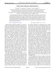
Time-resolved two-photon photoemission of metal/organic<br />
interface states<br />
U. Höfer 1 , M. Marks 1 , C. H. Schwalb 1 , B. Schmidt 2 , S. Sachs 2 , A. Schöll 2 , F. Reinert 2<br />
1 Fachbereich Physik und Zentrum für Materialwissenschaften,Philipps-Universität Marburg,<br />
Renthof 5, D-35032 Marburg, Germany<br />
2 Universität Würzburg, Experimentelle Physik II, Am Hubland, D-97074 Würzburg, Germany<br />
(corresponding author: U. Höfer, e-mail: hoefer@physik.uni-marburg.de)<br />
Time-resolved two-photon photoelectron spectroscopy (2PPE) can provide very detailed information<br />
about the dynamics of electron transfer processes at surfaces and interfaces. In order to exploit the full<br />
power of 2PPE for organic/metal interfaces it is desirable to investigate highly ordered epitaxial thin<br />
films on single-crystal surfaces as model systems. Such a system is 3,4,9,10-perylene-tetracarboxylic<br />
acid dianhydride (PTCDA) grown on Ag(111). The first monolayer of PTCDA/Ag(111) is<br />
chemisorbed with long-range order consisting of two flat lying molecules per unit cell that are<br />
arranged in a herringbone structure, similar to the crystal planes in the PTCDA bulk [1,2]. Therefore<br />
the higher molecular layers grow epitaxially on top of the first layer under certain conditions.<br />
The 2PPE spectra for PTCDA layers of<br />
various thicknesses display an unoccupied<br />
dispersing state between the metallic<br />
Fermi level and the lowest unoccupied<br />
molecular orbital (LUMO) of<br />
PTCDA (Fig. 1). The state corresponds<br />
to the one first observed by scanning<br />
tunnelling spectroscopy for a monolayer<br />
coverage [2]. Its energetic position in<br />
the band gaps of both the Ag(111) substrate<br />
and the PTCDA overlayer and the<br />
exponential weakening of the 2PPE<br />
intensity with film thickness identify it<br />
as a genuine interface state [3,4]. The<br />
lifetime of electrons excited into this<br />
interface state is 55 fs. This is a relatively<br />
small value for an unoccupied<br />
state located only 0.6 eV above the<br />
Fermi level. It is indicative for a large<br />
penetration of the wavefunction into the<br />
metal. Both, the large overlap with the<br />
Fig. 1 Measured dispersion of the interface state for<br />
1 ML (circles) and 2 ML (diamonds) of PTCDA<br />
together with the projected Ag(111) bulk bands<br />
(gray shaded area) and the Shockley state of the<br />
clean surface (dotted line). The borders of the<br />
PTCDA Brillouin zone for the two unit cell vectors<br />
are indicated by X1 and X2. (From Ref. [3], realspace<br />
structure after Ref. [1]).<br />
29
metal substrate and its small effective mass of 0.4 me suggest that the interface state originates mainly<br />
from the Shockley surface state of the bare Ag(111) surface which is strongly upshifted by the<br />
adsorption of PTCDA [3]. Recent DFT calculations show that the small molecular admixture of the<br />
state stems from of the LUMO+1 orbital of PTCDA that this admixture increases with increasing<br />
parallel momentum [5].<br />
Interface states that are located between the Fermi level of the metal and the LUMO level of organic<br />
molecules, such as the one observed for PTCDA/Ag(111), are expected to have a decisive influence<br />
on the charge carrier injection across a metal-organic interface. In order to gain insight into the<br />
mechanisms that lead to the formation of such interface states and to understand their properties we<br />
have investigated the smaller sister molecule of PTCDA, 1,4,5,8-naphtalene tetracarboxylic acid<br />
diandydride (NTCDA). We find a similar dispersing interface state that forms upon interaction with<br />
Ag(111). In agreement with the weaker interaction of this molecule with the metal substrate we<br />
observe a smaller upshift of the Shockley state and a longer electron lifetime as compared to<br />
PTCDA/Ag(111). In the disordered low-temperature phase of PTCDA, however, where the carboxyl<br />
groups bend down and interact more strongly with the metal surface than in the ordered PTCDA phase<br />
[6], we do not observe a further upshift of the interface state. Moreover, its lifetime is increased as<br />
compared to the ordered phase. We interpret these findings as an indication that the bending<br />
of the carboxyl groups causes the interface state to attain more overlap with the organic<br />
molecule.<br />
Funding by the Deutsche Forschungsgemeinschaft through SPP1093, SPP1121, GK790, and GK1221<br />
is gratefully acknowledged.<br />
[1] E. Umbach, M. Sokolowski, R. Fink, Appl. Phys. A, 63, 565 (1996)<br />
[2] R. Temirov, S. Soubatch, A. Luican, F. S. Tautz, Nature 444, 350 (2006)<br />
[3] C. H. Schwalb, S. Sachs, M. Marks, A. Schöll, F. Reinert, E. Umbach, U. Höfer, Phys. Rev. Lett. 101,<br />
146801 (2008)<br />
[4] S. Sachs, C.H. Schwalb, M. Marks, A. Schöll, F. Reinert, E. Umbach, U. Höfer, J. Chem. Phys. 131,<br />
144701 (2009)<br />
[5] M. S. Dyer, M. Persson, New J. Phys. 12, 063014 (2010)<br />
[6] L. Kilian et al., Phys. Rev. Lett. 100, 136103 (2008)<br />
30
Electronic properties of NiO thin films: A combined STM,<br />
STS, and 2PPE study<br />
Mario Kiel, Stephan Großer, Anke Höfer, Klaus Duncker, and Wolf Widdra<br />
Institute of Physics, Martin-Luther Universität Halle, 06120 Halle, Germany<br />
(Corresponding author: W. Widdra, e-mail: wolf.widdra@physik.uni-halle.de)<br />
By combining scanning tunneling microscopy and spectroscopy (STM, STS) with two-photon<br />
photoemission (2PPE) the electronic structure of ultrathin NiO(001) films has been<br />
investigated in the region of unoccupied states.<br />
For the 2PPE experiments a fiber-based laser system (IMPULSE, Clark-MXR) which drives<br />
two non-collinear optical parametric amplifiers at a repetition rate of 1.5 MHz is used. It<br />
delivers independently tunable laser beams in the<br />
range of 500 – 670 nm and 700 – 950 nm with pulse<br />
widths of 20 - 30 fs after compression. The photoelectron<br />
spectra have been recorded with a<br />
hemispherical electron energy analyzer (Phoibos<br />
150, Specs) which is equipped with a 2D<br />
channelplate detector. The STM and STS<br />
experiments have been performed in a different<br />
UHV chamber with a homebuilt instruments which<br />
is operated at 80 K.<br />
Based on STM for the NiO monolayer which has<br />
been grown by reactive metal deposition in an O2<br />
atmosphere on a Ag(001) substrate, an uniaxially<br />
compressed (2×1) structure is found as shown in<br />
Fig.1 (a). The NiO monolayer is characterized by<br />
two well-developed peaks in the corresponding STS<br />
spectra at 2.25 and 3.8 eV (Fig.1 (b)). For NiO films<br />
from 2 ML to 9 ML, STM and LEED show an<br />
Fig. 1: (a) STM image of 1.2 ML NiO deposited on<br />
Ag(001) at RT. (b) STS spectra in the region of<br />
unoccupied states for local NiO thickness of 1 and 2<br />
ML recorded at 80k. (c) Time-resolved two-color<br />
2PPE spectra for 2 ML NiO as function of pumpprobe<br />
delay.<br />
31
unreconstructed (1x1) structure as is expected for the NiO(001) rocksalt structure. With<br />
increasing layer thickness the STS spectra develop distinct variations as depicted in Fig. 1 (b)<br />
for the 2 ML film. Additionally for thicker layers a Ni3d-derived surface state develops<br />
within the band gap on NiO starting from 3 ML. It shifts in energy depending on the film<br />
thickness from 1.5 to 2.0 eV for 3 and 8 ML, respectively, as based on STS.<br />
Using two-color 2PPE the unoccupied electronic states are addressed in a alternative way as<br />
compared to STS. For the NiO monolayer the 2PPE spectra reveal a Ni 3d state at 3.73 eV<br />
above the Fermi energy which can be compared to STS spectra for defect-free NiO monolayer<br />
islands. Time-resolved data reveal a lifetime of approx. 35 fs for this state. A second<br />
unoccupied Ni 3d-derived state is identified in the 2PPE spectra at an energy of 2.4 eV for<br />
which the STS spectra exhibit again a clear feature. Additional features within the 2PPE<br />
spectra are assigned to photoemission from an occupied state at -0.34 eV. The time-resolved<br />
2PPE spectra for a 2 ML NiO film are depicted in Fig. 1 (c). Whereas the photoemission<br />
intensity which is visible at 3.2 eV in Fig. 1 (c) might be related to the unoccupied Ni 3d state<br />
at 2.8eV seen in STS, the 2PPE feature in the 3.9 – 4.4 eV region are tentatively assign to<br />
image potential states. The time-dependent intensities of all features show asymmetrical<br />
profiles which indicate finite lifetimes of the intermediate states.<br />
Support by the German joint research network Sonderforschungsbereich 762 “Functionality of oxidic interfaces”<br />
of the Deutsche Forschungsgemeinschaft is gratefully acknowledged.<br />
[1] S. Großer, C. Hagendorf, H. Neddermeyer, and W. Widdra, Surf. Interface Anal. 40, 1741-46 (2008).<br />
32
Epitaxy of Organic Nano-Fibers on Sheet Silicates:<br />
A Growth Model Based on Experiments and Simulations<br />
Claudia Ambrosch-Draxl1<br />
, C. Simbrunner2 , G. Hernandez-Sosa2 , D. Nabok1 ,<br />
M. Oehzelt2 , T. Djuric3 , R. Resel3 , L. Romaner1 , P. Puschnig1 , I. Salzmann4 ,<br />
G. Schwabegger2 , I. Watzinger2 , and H. Sitter2 1 Chair of Atomistic Modelling and Design of Materials,<br />
University of Leoben, A-8700 Leoben, Austria<br />
cad@unileoben.ac.at<br />
2 Johannes Kepler University Linz, Institute of Semiconductor and Solid State Physics,<br />
Johannes Kepler University, A- 4040 Linz Austria<br />
3 Technical University Graz, Institute of Solid State Physics,<br />
Graz University of Technology, A-8010 Graz, Austria<br />
4 Institut für Physik,<br />
Humboldt-Universität zu Berlin, D-12489 Berlin, Germany<br />
During the last years self-assembled organic nano-structures have been recognized as a proper<br />
fundament for several opto-electronic applications. In particular, phenylenes deposited on<br />
muscovite mica have turned out as an outstanding material combination. Epitaxial growth of<br />
phenylenes on muscovite mica results in the formation of parallel aligned nano-fibers,<br />
providing highly polarized emission in the blue spectral range (see Figure 1). Based on these<br />
optical properties, several applications have been demonstrated, e.g. waveguides, frequency<br />
doublers, and lasers.<br />
Currently, the epitaxial relation between muscovite mica as the substrate and organic nanoneedles<br />
has been explained by an interplay between electric fields and molecule-substrate<br />
interactions. It has been assumed that the presence of surface-dipole moments cause a fieldinduced<br />
dipole interaction between organic molecules and muscovite and thus significantly<br />
influences the molecular alignment during the initial phase of the growth process [1].<br />
By a combined theoretical and experimental approach, comprising x-ray diffraction (XRD)<br />
measurements, atomic-force microscopy (AFM), fluorescence microscopy, and force-field<br />
simulations, we present an alternative growth model being able to explain molecular<br />
33
adsorption on sheet silicates in terms of molecule-surface interactions only [2]. We<br />
demonstrate that geometrical changes in the substrate surface or molecule lead to different<br />
molecular adsorption geometries and needle directions which can be predicted by our growth<br />
model.<br />
We have chosen para-hexaphenyl (p6P) and sexithiophene (6T) as prototypical examples to<br />
substantiate our findings. To further support the crucial role of surface morphology, we have<br />
selected two different substrates, muscovite and phlogopite mica. We demonstrate that the<br />
presented model is able to explain our and also previously obtained experimental results.<br />
Figure 1: a) Observed needle orientations of organic molecules on muscovite mica with respect to the<br />
fluorescence emission wavelength. b) Fluorescence images of para-hexaphenyl (left) and sexithiophene (right)<br />
nano-fibers grown on muscovite mica.<br />
Support by the Fonds zur Förderung der Wissenschaftlichen Forschung, project S97, is gratefully acknowledged.<br />
[1] F. Balzer, H.-G. Rubahn, Appl. Phys. Lett. 79, 3860–3862 (2001).<br />
[2] C. Simbrunner, G. Hernandez-Sosa, D. Nabok, M. Oehzelt, T. Djuric, R. Resel, L. Romaner,<br />
P. Puschnig, C. Ambrosch-Draxl, I. Salzmann, G. Schwabegger, I. Watzinger, H. Sitter, preprint.<br />
34
Janus nanomembranes:<br />
Surfaces without bulk, functionalized on both sides<br />
Zhikun Zheng 1 , Christoph T. Nottbohm 1 , Andrey Turchanin 1 ,<br />
Heiko Muzik 1 , André Beyer 1 , Mike Heilemann 1 , Markus Sauer 2 , Armin Gölzhäuser 1<br />
1 Department of Physics, University of Bielefeld, Germany<br />
2 Biotechnology & Biophysics, Julius-Maximilians-University Würzburg, Germany<br />
A 1 nm thick free-standing membrane with amino functionalities on its top side and thiol<br />
functionalities on its bottom side was fabricated from aromatic self-assembled monolayers.<br />
It is demonstrated that such a bifacial Janus[1] membrane, is in fact a surface without a<br />
bulk that can act as a two dimensional platform for the selective immobilization of<br />
functional molecules[2]. We have functionalized both sides with different fluorescent<br />
molecules: The amino side of the membrane is modified with tetramethylrhodamine<br />
(TMR), the thiol side is functionalized with ATTO647N, cf. Fig.1. The successful<br />
immobilization of molecules is proven by XPS. Functionalized Janus nanomembranes<br />
cover areas up to several mm 2 and can be suspended over metal grids allowing a simple<br />
fluorescence detection, cf. Fig. 2. The potential of functionalized Janus nanomembranes as<br />
generic platform for two-dimensional directional chemistry is discussed.<br />
[1] Janus is a Roman god with two faces, see below.<br />
[2] Z. Zheng, C. T. Nottbohm, A. Turchanin, H. Muzik, A. Beyer, M. Heilemann, M. Sauer, A.<br />
Gölzhäuser: Janus nanomembranes: A generic platform for chemistry in two dimensions, Angewandte<br />
Chemie Intl. Ed. , 49, 8493 (2010).<br />
35
Fig.1: a) Schematic representation of the nanomembrane made from cross-linked biphenyl selfassembled<br />
monolayers. The 1 nm thick membrane has amino and thiol functional groups on its top and<br />
bottom sides, respectively. b) Schematic of the functionalization with fluorescent dyes of the top and<br />
bottom sides of the nanomembranes. The amino side is functionalized with TMR, symbolized by<br />
green dots the thiol side with ATTO647N, symbolized by the red dots. Subsequent functionalization<br />
of the top and the bottom sides yields a Janus nanomembrane.<br />
Fig. 2: Schematic and fluorescence micrographs of nanomembranes freely suspended over TEM grids:<br />
(a) amino side functionalized with TMR and (c) thiol side fuctionalized with ATTO647.<br />
Corresponding SEM micrographs: (b) and (d) show the same pieces of nanomembrane as (a) and (c),<br />
respectively.<br />
36
Electrochemical Generation of Low Dimensional Metal<br />
Structures on Top of Self-Assembled Monolayers<br />
Christophe Silien + , Manfred Buck*<br />
EaStCHEM School of Chemistry, University of St Andrews,<br />
North Haugh, St Andrews KY16 9ST, United Kingdom<br />
*mb45@st-and.ac.uk<br />
Low-dimensional metal structures in<br />
contact with molecules being of central<br />
importance for molecular electronics, their<br />
properties are poorly understood at<br />
present. It is not only the difficulty of a<br />
well-controlled preparation but also the<br />
theoretical understanding of the mutual<br />
influence of molecules and metal on their<br />
electronic properties which is at its<br />
infancy. However, studies performed so<br />
far indicate that new opportunities for<br />
Fig. 1: Architecture of a SAM illustrated by the<br />
example of a pyridine (blue) terminated aliphaticaromatic<br />
(grey) thiol (yellow).<br />
tailoring electronic properties arise from the<br />
combination of molecular systems with low<br />
dimensional metal structures [1-3].<br />
One strategy to study metal-molecule systems is<br />
based on self-assembled monolayers (SAMs) as<br />
SAMs offer a rich playground for fundamental<br />
studies due to the combination of properties.<br />
There is, firstly, the enormous flexibility in the<br />
tailoring of SAM properties both with regard to<br />
the surface of a SAM determined by the tail<br />
group and the design of the spacer unit (Fig. 1).<br />
Secondly, using a combination of aliphatic and<br />
aromatic moieties high quality SAMs can be<br />
generated whose surfaces exhibit a crystallinity<br />
closely resembling those of organic single<br />
crystals. Thirdly, charge transfer through SAMs<br />
Fig. 2: a) Illustration of electrochemical metal<br />
deposition on top of a SAM via the reduction of<br />
coordinated metal ions. b) STM image of Pd<br />
metal clusters deposited on a SAM.<br />
+ present address: Materials and Surface Science Institute and Department of Physics, University of Limerick, Ireland<br />
37
can be controlled via the spacer moiety.<br />
However the preparation of low dimensional metal structures in contact with a SAM is<br />
challenging as conventional procedures based on e.g. evaporation of metals onto SAMs are<br />
hard to control. A promising alternative approach is based on electrochemistry [ 4-7 ]. Owing to<br />
the particularities of the scheme the metal is confined to on top of the SAM, i.e. no shortcuts<br />
between the deposited metal and the substrate by penetration of metal into the SAM are<br />
produced. As illustrated in Fig. 2a the on top deposition is accomplished by an<br />
electrochemical process where the crucial point is that the metal ions are bound to the SAM<br />
via complexation. At sufficiently negative potentials the ions can be reduced and metal<br />
clusters are formed by diffusion of the atoms on the SAM surface as shown by the STM<br />
image in Fig. 2b. That the metal clusters are not in direct contact with the substrate is proven<br />
by the ease at which the clusters can be moved. The centre of Fig. 2b shows an area which has<br />
been wiped clean by the STM tip. Another piece of evidence comes from the observation of a<br />
Coulomb barrier when tunneling through a metal cluster.<br />
The complexation based deposition protocol allows precise control of the amount deposited<br />
and, thus, provides a unique way to low dimensional metal structures. The use of thiol SAMs<br />
of high structural integrity such as the one with the architecture shown in Fig. 1 significantly<br />
simplifies the previously reported two step scheme of complexation and reduction to a single<br />
step.<br />
Support by EPSRC is gratefully acknowledged.<br />
[1] H. G. Boyen, P. Ziemann, U. Wiedwald, V. Ivanova, D. M. Kolb, S. Sakong, A. Gross,<br />
A. Romanyuk, M. Buttner, and P. Oelhafen, Nature Materials 5, 394 (2006).<br />
[2] J. Kucera and A. Gross, Phys. Chem. Chem. Phys. 12, 4423 (2010).<br />
[3] J. A. Keith and T. Jacob, Chem. Eur. J. 16, 12381 (2010).<br />
[4] T. Baunach, V. Ivanova, D. M. Kolb, H. G. Boyen, P. Ziemann, M. Buttner, and P.<br />
Oelhafen, Adv. Mater. 16, 2024 (2004).<br />
[5] O. Shekhah, C. Busse, A. Bashir, F. Turcu, X. Yin, P. Cyganik, A. Birkner, W.<br />
Schuhmann, and C. Woll, Phys. Chem. Chem. Phys. 8, 3375 (2006).<br />
[6] D. Qu and K. Uosaki, J. Phys. Chem. B 110, 17570 (2006).<br />
[7] C. Silien, D. Lahayee, M. Caffio, R. Schaub, N. R. Champness, and M. Buck, Langmuir<br />
(in press).<br />
38
Charge Transport Through and Within Self-Assembled Monolayers:<br />
New Insights from Nanofabricated Model Devices<br />
Christof Wöll<br />
Institute of Functional Interfaces (IFG), Karlsruhe Institute of Technology, KIT, 76344 Karlsruhe<br />
E-mail: Christof.Woell@KIT.edu, www.ifg.kit.edu<br />
The use of organic molecules as active<br />
semiconductors in electronic devices is reaching<br />
the stage where commercial products are arriving<br />
at the market. There are, however, still a number<br />
of fundamental issues, e.g. a proper description of Fig. 1: Schematic diagram of an “ideal” organic<br />
diode with two tunnel contacts [3].<br />
phenomena (e.g. charge injection) occurring at the<br />
electrode/OSC interface. Unfortunately, there are pronounced problems with growing highly<br />
ordered OSC-films on (strictly clean) metal substrate [1]. An attractive alternative to produce<br />
well-defined interfaces also suited for a theoretical analysis is to modify the metal electrode by<br />
adsorbing a well-defined thiolate-based self-assembled monolayer (SAM) [2]. This approach not<br />
only allows adjusting the work-function of the metal, but also provides structurally perfect<br />
substrates well suited for the OMBD-process.<br />
In this talk we will demonstrate that on an Au substrate covered with a decanethiolate SAM,<br />
pentacene, one of the most interesting molecules to be used as organic semiconductor in OFETs, can<br />
be grown in a rather perfect, bulk-like structure. The high structural quality and the absence of any<br />
contaminations make it possible to produce a two-terminal organoelectronic model device as shown<br />
in Fig. 1 [3]. This “ideal” device is essentially free of imperfections and well suited for a theoretical<br />
analysis. The results of numeric simulations [3] reveal that, at positive bias, n-transport dominates<br />
p-transport, an unusual behavior for pentacene-based devices.<br />
The n-conduction within the OSC pentacene can be suppressed by introducing OH-groups at the<br />
SAM/OSC interface, a finding which is in accord with related experiments on OFETs [4]. Recent<br />
experiments indicate that loading of the OH-traps with electrons is a reversible process [5].<br />
Fabrication of functioning OFET devices confirms the positive effect of SAM surface modification<br />
on device properties [6].<br />
A recent investigation of nanographene-based SAMs has demonstrated that using the<br />
SAM-approach relative molecular orientations can be achieved which are different from that present<br />
in the corresponding bulk phases, with very positive effects on the charge carrier mobilities [7].<br />
References<br />
[1] G.Witte and Ch.Wöll, J.Mater.Res. 19, 1889 (2004)<br />
[2] M. Kind and C. Wöll, Prog. Surf. Sci. 84, 230 (2009)<br />
[3] L.Ruppel, A.Birkner, G.Witte, C.Busse, T.Lindner, G.Paasch, C.Wöll, J.Appl.Phys. 102,<br />
033708 (2007)<br />
[4] L.Chua, J.Zaumseil, J.Chang, E.Ou, P.Ho, H.Sirringhaus, R.Friend, Nature 434, 194 (2005)<br />
[5] Z.-H. Wang, D. Käfer, A. Bashir, J. Götzen, A. Birkner, G. Witte, Ch. Wöll,<br />
PhysChemChemPhys, 12, 4317-4323 (2010)<br />
[6] C.Bock, D.Pham, U.Kunze, D.Käfer, G.Witte, Ch.Wöll, J.Appl.Phys. 100, 114517 (2006)<br />
[7] D. Käfer, A. Bashir, X. Dou, G. Witte, K. Müllen, Ch. Wöll, Adv. Mater, 22, 384-388 (2010)<br />
39
Tuesday 8 th March <strong>2011</strong>
Gold clusters at finite temperature in vacuo and in a CO<br />
plus O2 atmosphere:<br />
ab initio studies towards gold catalysis<br />
Elizabeth C. <strong>Beret</strong>, Luca M. Ghiringhelli, Merel M. van Wijk,<br />
and Matthias Scheffler<br />
Fritz Haber Institute of the Max Planck Society,<br />
Faradayweg 4-6, D-14195 Berlin-Dahlem, Germany<br />
(corresponding author: M. Scheffler, Scheffler@FHI-Berlin.mpg.de)<br />
The marked catalytic activity of gold nanoparticles has inspired a large number of scientific<br />
contributions. However, many questions still lack a satisfying answer, for example, what are<br />
the structures and stoichiometries of gold particles at realistic temperatures, in the presence of<br />
(reactive) gases, and how do they change with particle size. We address these issues for gold<br />
clusters, focusing on AuN with 3 ≤ N ≤ 20, modeled in vacuo as well as in an atmosphere<br />
containing CO and O2 in variable compositions. We combine all-electron density-functional<br />
theory, including density-dependent van-der-Waals tail corrections, with finite temperature<br />
sampling techniques, like Biased Molecular Dynamics (MD) and Parallel Tempered MD.<br />
The results show that at temperatures as low as 100 K vibrational spectra already display<br />
noticeable anharmonic features. At room temperature the flexibility of the clusters is already<br />
significant, and certain AuN clusters may be better described as liquid droplets. This has<br />
important implications for adsorption of atoms or molecules because the energy released by<br />
an exothermal adsorption heats up the complex, and in the gas phase the time to reach thermal<br />
equilibrium with the environment is much longer than the cluster conformational<br />
rearrangements. Thus, the concept of a preferred adsorption site becomes questionable.<br />
Taking the CO oxidation reaction as example, we address the above-mentioned questions for<br />
very small neutral and anionic gold clusters modeled in a gas-phase atmosphere containing<br />
CO and O2 as function of partial pressures and temperature. To this aim, DFT (PBE)–based<br />
ab initio atomistic thermodynamics is applied, including the vibrational contributions to the<br />
free energy. As a result, the preferred cluster+adsorbate structures for different environmental<br />
conditions are obtained and interpreted as candidate intermediates in the catalytic CO<br />
oxidation reaction. Furthermore, we discuss the different behavior of the system in two<br />
different kinds of conditions: a) a situation where the product CO2 is constantly removed<br />
from the system (like in a flow reactor) and b) a situation where equilibrium with the product<br />
CO2 is reached.<br />
42
Defects on room temperature ultra-thin<br />
film CeO 2 with STM<br />
D.C. Grinter, R. Ithnin, C.L. Pang, G. Thornton<br />
London Centre for Nanotechnology and Department of Chemistry,<br />
University College London, 20 Gordon Street, London, WC1H 0AJ, UK<br />
(corresponding author, email: g.thornton@ucl.ac.uk)<br />
The study of ceria (CeO 2) is currently of great interest, with proven technological applications<br />
arising from its wide-ranging catalytic properties including exhaust gas purification in<br />
automotive catalytic converters and in the water gas shift reaction to produce H2. 1 The key to<br />
these properties lies in the high mobility of lattice oxygen leading to excellent oxygen storage<br />
and release, thought to be determined by the nature, concentration and mobility of lattice<br />
defects, especially oxygen vacancies. A further potentially important role of vacancies is in<br />
the binding of catalytically active metals such as Au, recently discovered to be a highly active<br />
catalyst for the water-gas-shift reaction. 2,3<br />
As ceria is an insulator with a band gap of 6 eV, ultra-thin films of CeO 2(111) were prepared<br />
on a conducting substrate of Pt(111) to permit room temperature studies with scanning<br />
tunnelling microscopy (STM). The ultra-thin films were grown in two ways: by reactive<br />
deposition in an oxygen atmosphere, and by post-oxidation of Ce/Pt surface alloys.<br />
Atomically resolved STM images of films prepared by both methods revealed remarkable<br />
similarities to images recorded in previous studies on CeO 2(111) single crystals using NC-<br />
AFM and high temperature STM. Surface oxygen vacancies were imaged individually, as<br />
trimers, and in linear arrays. Subsurface oxygen vacancies were also detected as well as<br />
adsorbed water molecules and surface hydroxide trimers, again with a similar appearance to<br />
that seen on native CeO2(111) 4,5 , with agreement for point defects in filled state images of<br />
6<br />
thin film CeO2 (see fig 1). As such, we conclude that ultra-thin ceria films supported on<br />
Pt(111) make excellent topographic models for the native oxide.<br />
43
Figure 1: Atomically resolved, filled states, STM image (5 x 4 nm 2 , V s = -3.20 V, I t = 0.20<br />
nA) and structural model of vacancies and adsorbates on an ultra-thin film of CeO 2(111) on<br />
Pt(111). Bright spots correspond to top layer oxygen termination of surface, with<br />
identification of adsorbed water, hydroxide trimers and surface oxygen vacancies possible by<br />
comparison with NC-AFM 4 and high temperature STM 5 . The assignments are highlighted in<br />
the structural model. Water molecules are observed exclusively above second layer Ce<br />
atoms.<br />
(1) Trovarelli, A. Catalysis by Ceria and Related Materials: Imperial College Press:<br />
London 2000 Vol 2<br />
(2) Fu, Q et al. Science 2003, 301, 935-938<br />
(3) Liu, Z. et al. Phys. Rev. Lett. 2005, 94, 196102<br />
(4) Gritschneder, S.; Iwasawa, Y.; Reichling, M. Nanotech. 2006, 18, 044025; Phys.<br />
Rev. Lett. 2007, 99, 056101<br />
(5) Esch, F.; Fabris, S.; Zhou, L.; Montini, T.; Africh, C.; Fornasiero, P.; Comelli, G.;<br />
Rosei, R. Science 2005, 309, 752-755<br />
(6) Eck, S.; Castellarin-Cudia, C.; Surnev, S.; Ramsey, M. G.; Netzer, F. P. Surf. Sci.<br />
2002, 530, 173-185<br />
44
High Island Densities in Pulsed Laser Deposition: Causes and Implications<br />
Peter Varga<br />
Institute for Applied Physics, Vienna University of Technology, Vienna, Austria<br />
Pulsed laser deposition (PLD) is a versatile deposition method that combines many<br />
features of technologically relevant processes such as sputter deposition with ultrahighvacuum<br />
compatibility and easy accessibility by surface science methods. PLD is<br />
characterized by high energies of the impinging particles (ions) and known to lead to<br />
higher island densities and better layer-by-layer growth than conventional thermal<br />
deposition. We have studied homoepitaxy of Pt on Pt(111) as well as heteroepitaxy of Co<br />
on Pt(111) by PLD with scanning tunneling microscopy (STM) [1]. For heteroepitaxy of<br />
Co on Pt(111), atomically resolved STM with chemical contrast shows implantation of<br />
impinging species in the surface. By directly watching diffusion processes, we<br />
demonstrate that the resulting heterogeneous surface impedes surface diffusion, leading<br />
to exceptionally high island densities. For homoepitaxy with moderate ion energies (<<br />
100 eV), comparison with nucleation theory shows that the high island densities are<br />
merely caused by the high instantaneous flux of arriving particles, while the kinetic<br />
energy of the impinging particles plays no significant role. At higher ion energies (> 200<br />
eV), however, additional nuclei are formed by ``failed sputtering'', i.e., formation of adatoms<br />
by the impinging energetic ions. Layer-by-layer growth observed in PLD<br />
experiments down to very low temperatures can be explained by the small island size and<br />
implantation of energetic particles.<br />
Nucleation of small Pt clusters shows another unexpected phenomenon: We found a large<br />
number of linear chains, with lengths of up to 9 atoms. This result cannot be explained by<br />
a simple diffusion-limited-aggregation model, and we suggest that the strain field of the<br />
substrate plays an important role, steering some of the diffusing adatoms towards the<br />
ends of linear clusters. As a further ingredient to this phenomenon, a study of the binding<br />
energies of Pt adatom clusters by DFT shows that bonding of such clusters does not<br />
follow the rule of "higher coordination means stronger bonding". Instead, short linear<br />
chains are bound more strongly than more compact configurations. The reason for this<br />
phenomenon is strong directional bonding via d z2-like orbitals, a mechanism previously<br />
proposed for binding between the late transition metals and oxygen atoms and explaining<br />
the preference for O atoms at opposite sides of a metal atom.<br />
1 M.Schmid, C.Lenauer, A.Buchsbaum, F.Wimmer, G.Rauchbauer, P.Scheiber, G.Betz,<br />
and P.Varga, Phys.Rev.Lett. 103 (2009) 076101<br />
45
Copper electrodeposition on fast time scale: from<br />
underpotential deposition to bulk growth<br />
Y. Yanson, J. W. M. Frenken, M. J. Rost<br />
Kameringh Onnes Laboratory, Leiden University,2333CA Leiden , the Netherlands<br />
(corresponding author: Y. Yanson, e-mail: yansony@physics.leidenuniv.nl)<br />
Copper electrodeposition has drawn a lot of attention in the last two decades. One reason for<br />
that is its increasing relevance for industrial applications [1]. Another reason is that Cu<br />
electrodeposition on substrates from different metals, especially gold, became a „benchmark“<br />
system for studying adsorption and deposition phenomena at solid/liquid interfaces. In fact,<br />
Cu underpotential deposition (UPD), i.e. deposition of a single monoatomic layer, has<br />
become a system of choice for testing different surface-sensitive techniques [2].<br />
Despite the vast amount of literature on Cu electrodeposition, there are still a lot of<br />
controversies and open questions concerning the system. For example, there are some<br />
contradictions in the results found in literature on Cu UPD onto metallic substrates covered<br />
by self-assembled monolayers (SAM) of thiol molecules [3-5]. Also, the more applicationwise<br />
relevant Cu deposition regime, i.e. Cu bulk deposition, has been merely studied,<br />
especially at its initial stages [6,7]. The reason for this is that the bulk deposition process<br />
happens too rapid 1 for the conventional scanning probe techniques to capture it.<br />
Figure 1. Cu UPD layer formation a) on a clean Au(111) surface and b) on the surface<br />
covered by a SPS 2 SAM.<br />
We have developed a new fast electrochemical scanning tunneling microscope (EC-STM),<br />
which allows us to obtain information about the dynamics of the UPD processes, see Fig. 1,<br />
and also gives us the possibility to follow the bulk Cu electrodeposition in-situ. From the EC-<br />
STM measurements combined with electrochemical cyclic voltammetry (CV) measurements<br />
46
we were able to develop a model, which describes well UPD onto metallic single crystal<br />
surfaces covered by thiol SAMs. Although our model was developed for a particular case of<br />
Cu UPD onto the Au(111) surface covered by a SPS 2 SAM, many results on different systems<br />
found in literature can be well described by it.<br />
Our EC-STM also gives us the possibility to take a glimpse at the initial stages of the Cu bulk<br />
deposition. We compare Cu bulk deposition onto Au(111) surface from an additive-free<br />
solution and a SPS-containing one, see Fig. 2. We demonstrate that our EC-STM can provide<br />
information on e.g. the influence of the SPS onto the nucleation density and feature size of the<br />
Cu deposit. Such parameters can not be easily extracted from conventional electrochemical<br />
measurements.<br />
a) b)<br />
Figure 2. Bulk Cu deposition from a solution a) without b) with SPS.<br />
1 at relevant Cu 2+ ion concentrations in the solution<br />
2 Bis(3-sulfopropyl)disulfide<br />
[1] P. C. Andricacos, C. Uzoh, J. O. Dukovic, J. Horkans, H. Deligianni, IBM Jour. Res. and Dev. 42, 567<br />
(1998)<br />
[2] M. E. Herrero, J. L. Buller, D. H. Abruna, Chemical Review 101, 1897 (2001)<br />
[3] M. A. Schneeweiss, H. Hagenstrom, M. J. Esplandiu, D. M. Kolb, Applied Physics A:Materials Science &<br />
Processing 69, 537 (1999)<br />
[4] M. Petri, D. M. Kolb, U. Memmert, H. Meyer, Electrochimica Acta 49, 183 (2003).<br />
[5] C. Silien and M. Buck, Journal of Physical Chemistry C 112, 3881 (2008)<br />
[6] A. I. Danilov, E. B. Molodkina, A. V. Rudnev, Yu. M. Polukarov, J. M. Feliu, Electrochim. Acta 50, 5032<br />
( 2005)<br />
[7] N. Batina, T. Will, M. D. Kolb, Faraday Discussions 94, 93 (1992)<br />
47
Buckling under tension – LaAlO3 on SrTiO3<br />
1 1 1 1 1<br />
Phil Willmott , Stephan Pauli , Steven Leake , Bernard Delley , Christof Schneider , Jochen<br />
Mannhart 2 , and Stefan Paetel 2 ,<br />
1. Paul Scherrer Institut,CH-5232 Villigen Switzerland<br />
(corresponding author: P.R. Willmott, e-mail: Philip.willmott@psi.ch)<br />
2 Lehrstuhl für Experimentalphysik VI, Universität Augsburg, Universitätstr. 1, D-86135 Augsburg,<br />
Germany<br />
Since its discovery in 2004 [1], the conducting interface between the band insulators SrTiO3<br />
(STO) and LaAlO3 (LAO) has been the subject of intense research [2]. Several propositions<br />
have been made to explain this phenomenon, including oxygen vacancies [3], electronic<br />
reconstruction [1], intermixing [4], and dipole compensation through buckling [5]<br />
One of the most intriguing clues to this complex phenomenon was the discovery that<br />
conductivity at the interface only occurs if four or more monolayers (MLs) of LAO are<br />
deposited [6]. This would seem to indicate that subtle structural variations might play a<br />
pivotal role in determining the physical processes at play. The only technique capable of<br />
determining the atomic structure with sufficient accuracy (of the order of 10 pm or better) is<br />
surface x-ray diffraction (SXRD) [4].<br />
In this presentation, I will discuss systematic changes to the atomic structure of the STO/LAO<br />
system as one progresses from two to five monolayers, as determined from comprehensive<br />
SXRD data [7], analyzed using model-free phase-retrieval methods [8]. The interfacial<br />
conductivity is explained in terms of intermixing, dipole formation as a result of buckling, and<br />
electronic transfer. DFT calculations will also be presented.<br />
[1] A. Ohtomo and H.Y. Hwang, “A high-mobility electron gas at the LaAlO3/SrTiO3 heterointerface,” Nature<br />
427, 423 (2004)<br />
[2] S.A. Pauli and P.R. Willmott, “Conducting interfaces between polar and non-polar insulating perovskites,”<br />
J. Phys.: Condens. Matter 20, 264102 (2008)<br />
[3] Siemons et al., “Origin of charge density at LaAlO3 on SrTiO3 heterointerfaces: possibility of intrinsic<br />
doping,” Phys. Rev. Lett. 98, 196802 (2007)<br />
[4] P.R. Willmott et al., “Structural basis for the conducting interface between LaAlO3 and SrTiO3,” Phys. Rev.<br />
Lett. 99, 155502 (2007)<br />
[5] R. Pentcheva and W.E. Pickett, “Avoiding the Polarization Catastrophe in LaAlO3 Overlayers on<br />
SrTiO3(001) through Polar Distortion,” Phys. Rev. Lett. 102, 107602 (2009)<br />
48
[6] S. Thiel et al., “Tunable Quasi-Two-Dimensional Electron Gases in Oxide Heterostructures,” Science. 313,<br />
1942 (2006)<br />
[7] S.A. Pauli et al., “Evolution of the Interfacial Structure of LaAlO3 on SrTiO3,” Phys. Rev. Lett. 106,<br />
036101 (<strong>2011</strong>)<br />
[8] M. Björck et al., “Atomic imaging of thin films with surface x-ray diffraction: introducing DCAF,” J. Phys.:<br />
Condens. Matter 20, 445006 (2008)<br />
49
Dewetting dynamics of crystalline thin films<br />
E. Bussmann 1 , F.Leroy 1 , F.Cheynis 1 , O.Pierre-Louis 2 , P.Müller 1<br />
1 CINaM, UPR 3118 CNRS, Aix-Marseille Université ,<br />
Campus de Luminy, case 913, F-13288 Marseille Cedex 9, France<br />
2 LPMCN, Université de Lyon, 69622 Villeurbane Cédex<br />
cheynis@cinam.univ-mrs.fr<br />
Thin solid films are the basic components in many devices. However since the deposition<br />
conditions generally are far from equilibrium, such 2D thin films, when annealed, may break<br />
up into 3D islands. This so-called dewetting process is observed in many experimental<br />
systems. If a continuous film is required for applications, dewetting clearly is a limiting<br />
process. On the other hand it appears to be a cheap and easy-to-implement method to produce<br />
and control the formation of an assembly of nanocrystals.<br />
Here we report a quantitative characterization of<br />
the dewetting dynamics of silicon-on-oxyde (SOI)<br />
thin-films. From an experimental point of view we<br />
use Low-Energy Electron Microscopy (LEEM) to<br />
record real-time in-situ movies of the dynamics of<br />
the SOI dewetting process leading to the formation<br />
of 3D compact Si nanocrystals. The complex<br />
morphological evolution is reproduced by a simple<br />
Solid-on-Solid Kinetic Monte Carlo (KMC) model<br />
in which enter only two physical ingredients: a<br />
wetting parameter and a reduced temperature. As<br />
shown in the nearby figure the KMC model<br />
reproduces the qualitative features of the<br />
morphological evolution (See Fig. a and b) as well<br />
as the growth dynamics.<br />
To get insight into the global dynamics we develop<br />
analytic models that capture the essentials of the<br />
underlying physics and enable us to clearly identify<br />
the origin of the driving-force. Our results show (i)<br />
that the dewetting is a consequence of surface freeenergy<br />
minimization mediated by surface diffusion<br />
and (ii) that the velocity of the dewetting front is<br />
limited by its thickening. We connect the rim<br />
growth mechanism to the growth dynamics of the<br />
Fig: Dewetting morphology versus time: (a)<br />
AFM and LEEM results. (b) KMC<br />
dewetted area. The front edges instabilities that lead to the formation of local elongated<br />
structures (then to 3D islands by a pinch-off process) are closely connected to the local height<br />
instabilities of the rim.<br />
Finally the dewetting properties of SOI films are compared to those obtained for a few<br />
other systems.<br />
Reference:<br />
E. Bussmann, F.Cheynis, F.Leroy, P.Müller, O.Pierre-Louis, Dynamics of solid thin-film<br />
dewetting in the silicon-on-insulator system, NJP Submitted<br />
50
The role of dispersion forces in the structure of graphene<br />
monolayers over the Ru(0001) surface<br />
D. Stradi, 1,2 S. Barja, 3,2 C. Díaz, 1 M. Garnica, 3,2 B. Borca, 3 J. J. Hinarejos, 3 D. Sánchez-<br />
Portal, 4,5 M. Alcamí, 1 A. Arnau, 4, 5, 6 A. L. Vázquez de Parga, 3, 2 R. Miranda, 3, 2 and F. Martín 1,2<br />
(corresponding author: F. Martín, e-mail: fernando.martin@uam.es)<br />
1 Departamento de Química, Módulo 13, Universidad Autónoma de Madrid, 28049 Madrid, Spain<br />
2 Instituto Madrileño de Estudios Avanzados en Nanociencia (IMDEA-Nanociencia), Cantoblanco,<br />
28049 Madrid, Spain<br />
3 Dep. Física de la Materia Condensada, Universidad Autónoma de Madrid, 28049 Madrid, Spain<br />
4 Materials Physics Center (CSIC-UPV/EHU), Paseo Manuel de Lardizábal 5, 20018 San Sebastián,<br />
Spain<br />
5 Donostia International Physics Centre (DIPC), Paseo Manuel Lardizábal 4, 20018 San Sebastián,<br />
Spain<br />
6 Dep. Física de Materiales (UPV/EHU), Facultad de Química, Apartado 1072, 20080 San Sebastián,<br />
Spain<br />
The electronic properties of perfect graphene makes it a promising material for applications in<br />
microelectronics and sensing. In practice, the synthesis of graphene can be achieved by<br />
epitaxial growth of carbon monolayers on transition metals [1]. In many cases, such as in<br />
graphene grown on Ru(0001) (G/Ru for short), the mismatch between the lattice constant of<br />
graphene and the one of the substrate leads to the appareance of a Moiré pattern [2]. This<br />
results in substantial modifications in graphene morphology, which is periodically corrugated,<br />
and in its electron density, which is no longer uniform [3]. Such properties are responsible for,<br />
e.g., the formation of quantum dots [4,5] or site selective deposition of organic molecules [6].<br />
Despite numerous efforts to determine the morphology of the Moiré observed in G/Ru, the<br />
actual value of the corrugation is still a subject of controversy. Depending on the<br />
experimental technique employed, very different values are obtained, which fall in the broad<br />
range 0.4Å – 1.5Å [3,7,8]. On the theoretical side, Density Functional Theory (DFT)<br />
calculations predict a corrugation in the range 1.5Å – 1.7Å [9,10,11].<br />
51
Standard DFT is not capable to account for long range van der Waals (vdW) interactions.<br />
However, there is strong evidence that these forces play a crucial role in the adsorption of<br />
aromatic molecules on metal surfaces [12,13,14], leading to a significant increase of the<br />
calculated adsorption energies and, what is even more important, to significant modifications<br />
of the adsorption geometry [15]. In many respects, graphene can be considered as an extended<br />
aromatic system due to the presence of a π electronic cloud above and below the graphene<br />
plane. Therefore, it is worth studying if vdW interactions play a similar important role in the<br />
structure of graphene lying on top of a metal substrate.<br />
In the present work, using DFT calculations in which effect of vdW interactions is included,<br />
we show that such interactions lead to a substantial reduction of the corrugation with respect<br />
to standard DFT calculation. Qualitative agreement is obtained with the apparent height<br />
variations near the Fermi level observed in STM and structural data obtained both from Low<br />
Energy Electron Diffraction (LEED) and Surface X-Ray Diffraction (SXRD).<br />
Mare Nostrum BSC and CCC-UAM for computer time are kindly acknowledged. Work supported by the<br />
MICINN projects FIS2010-15127, FIS2010-18847, FIS2010-19609-C02-00, ACI2008-0777 and 2010C-07-<br />
25200, the CAM program NANOBIOMAGNET S2009/MAT1726, and the Gobierno Vasco - UPV/EHU project<br />
IT-366-07.<br />
[1] J. Wintterlin and M. L. Bocquet Surf. Sci. 603, 1841 (2009)<br />
[2] S. Marchini and S. Günther and J. Wintterlin Phys. Rev. B 76, 075429 (2007)<br />
[3] A. L. Vázquez de Parga and F. Calleja and B. Borca and M. C. G. Passeggi Jr. and J. J. Hinarejos and F.<br />
Guinea and R. Miranda Phys. Rev. Lett. 100, 056807 (2008); Phys. Rev. Lett. 101 099704 (2008)<br />
[4] B. Borca and S. Barja and M. Garnica and D. Sánchez-Portal and V. M. Silkin and E. V. Chulkov and C. F.<br />
Hermanns and J. J. Hinarejos and A. L. Vázquez de Parga and A. Arnau and P. M. Echenique and R.<br />
Miranda Phys. Rev. Lett. 105, 036804 (2010); Phys. Rev. Lett. 105, 219702 (2010)<br />
[5] H. G. Zhang, H. Hu, Y. Pan, J. H. Mao, M. Gao, H. M. Guo, S. X. Du, T. Greber, and H.-J. Gao, J. Phys.:<br />
Condens. Matter 22, 302001 (2010); Phys. Rev. Lett. 105, 219701 (2010)<br />
[6] J. Mao and H. Zhang and Y. Jiang and Y. Pan and M. Gao and W. Xiao and H.-J. Gao J. Am. Chem. Soc.<br />
131, 14136 (2009)<br />
[7] D. Martoccia, P. R. Willmott, T. Brugger, M. Björck, S. Günther, C. M. Schlepütz, A. Cervellino, S. A.<br />
Pauli, B. D. Patterson, S. Marchini, et al., Phys. Rev. Lett. 101, 126102 (2008)<br />
[8] D. Martoccia, M. Björck, C. M. Schlepütz, T. Brugger, S. A. Pauli, B. D. Patterson, T. Greber, and P. R.<br />
Willmott, New J. Phys. 12, 043028 (2010)<br />
[9] W. Moritz, B. Wang, M. L. Bocquet, T. Brugger, T. Greber, and J. Wintterlin, Phys. Rev. Lett. 104, 136102<br />
(2010)<br />
[10] B. Wang, M. L. Bocquet, S. Marchini, S. Günther, and J. Wintterlin, Phys. Chem. Chem. Phys. 10, 3530<br />
(2008); Phys. Rev. Lett. 101, 099703 (2008); New J. Phys. 12, 043041 (2010)<br />
[11] D. Jiang, M.-H. Du, and S. Dai, J. Chem. Phys. 130, 074705 (2009)<br />
[12] P. Sony, P. Puschnig, D. Nabok, and C. Ambrosch-Draxl, Phys. Rev. Lett. 99, 176401 (2007)<br />
[13] N. Atodiresei, V. Caciuc, P. Lazic, and S. Blügel, Phys.Rev. Lett. 102, 136809 (2009)<br />
[14] G. Mercurio, E. R. McNellis, I. Martin, S. Hagen, F. Leyssner, S. Soubatch, J. Meyer, M. Wolf, P. Tegeder,<br />
F. S. Tautz, et al., Phys. Rev. Lett. 104, 036102 (2010)<br />
[15] E. R. McNellis, J. Meyer, K. Reuter, Phys. Rev. B 80, 205414 (2009)<br />
52
Growth of graphene nanoislands on a Ni(111) surface<br />
G. Ceballos, M. Ollé. P. Gambardella<br />
CIN2(ICN-CSIC), Catalan Institute of Nanotechnology, Campus de la UAB 08193 Bellaterra<br />
(Barcelona) Spain<br />
Since they first time a layer of graphene was isolated in 2004 [1], the interest in this material<br />
increased exponentially. The main attraction of this material lies in their unusual and<br />
surprising electronic, mechanical and magnetic properties such as the anomalous quantum<br />
Hall effect, the absence of electronic localization, high optical transparency, the high<br />
electrical conductivity, flexibility and high mechanical strength. These properties make<br />
graphene a very promising material for applications in electronics and spintronics, and<br />
therefore it is necessary to control the growth and properties at the nanoscale.<br />
The growth of graphene layers on the nickel surface by decomposition of hydrocarbons is<br />
interesting for three main reasons. On the one hand, the lattice constant of the surface of<br />
Ni(111) coincides almost perfectly with the lattice constant of graphene, which allows it to<br />
grow in a (1×1) structure. Moreover, due to the catalytic effect of nickel surface, it is a<br />
autoterminated reaction, i.e., the reaction stops once the graphene monolayer is formed<br />
avoiding the growth of multilayers [2]. Finally, the Nickel is a ferromagnetic material, which<br />
opens the door to applications in spintronics.<br />
Progress in the manufacture of low dimensional structures such as graphene nanoribbons has<br />
been reported [3]. It shows that the electronic properties of graphene change in a non-trivial<br />
way going to nanoscopic dimensions mainly due to the contribution of edge effects. Several<br />
theoretical studies have focused on the properties<br />
of the edges of graphene nanocrystals [4-7]. In the<br />
case of zig-zag edges of triangular nanocrystals a<br />
particularly high magnetic moment has been<br />
predicted [8].<br />
In this work we study by STM the growth of<br />
graphene on a Ni (111) surface by decomposition<br />
of hydrocarbons. By varying parameters such as<br />
the dosage of hydrocarbon, reaction time and<br />
temperature was possible to obtain in a<br />
reproducible manner a wide range of coverages.<br />
For low coverages the carbon atoms organize<br />
themselves into graphene nanoislands whose size<br />
and density are related to the reaction parameters.<br />
These nanoislands, initially with irregular shapes,<br />
53<br />
Figure 1: STM image (8x8nm) of a<br />
graphene nanoisland on a Ni(111<br />
surface).
may, by further thermal treatment selectively acquire a triangular (Fig. 1) or hexagonal shape<br />
both with zig-zag edges. In the case of triangular islands all edges have the same packaging<br />
with the nickel surface underneath while in the case of hexagonal islands edges change<br />
alternatively the packaging. The optimum conditions to obtain nanoislands of particular size<br />
and shape are studied by systematic variation of the parameters of the hydrocarbon<br />
decomposition reaction and the thermal diffusion of carbon on the surface.<br />
[1] K.S. Novoselov et al, Science, 306, 666-669 (2004).<br />
[2] J. Wintterlin, M.-L. Bocquet, Surface Science, 603, 1841–1852, (2009)<br />
[3] M.Y. Han et al., Phys. Rev. Lett. 98, 206805 (2007).<br />
[4]A. Kuc, T. Heine and G. Seifert, Phys. Rev. B 81, 085430 (2010).<br />
[5] W.L. Wang, S. Meng, and E. Kaxiras, Nano Lett. 8(1), 241-245 (2008).<br />
[6] T. Nakajima and K. Shintani, J. App. Phys. 106, 114305 (2009)<br />
[7] W.L. Wang, O.V. Yazyev, S. Meng, E. Kaxiras, Phys. Rev. Lett. 102, 157201 (2009).<br />
[8] J.Fernández-Rossier and J.J. Palacios, Phys. Rev. Lett. 99, 177204 (2007).<br />
54
Kinetics of graphene growth on Rh(111)<br />
G. Dong, D.W. van Baarle, M.J. Rost and J.W.M. Frenken<br />
Kamerlingh Onnes Laboratory, Leiden University, PO Box 9504, 2300 RA Leiden, The Netherlands<br />
(corresponding author: J.W.M. Frenken, e-mail: Frenken@physics.leidenuniv.nl)<br />
Graphene, single-layer graphite, is drawing much attention because of its special<br />
properties and potential use in future-generation electronics [1]. A practical and<br />
promising method for mass production of graphene is hydrocarbon chemical vapor<br />
deposition (CVD) on metal surfaces. Metal surfaces which are catalysts for<br />
hydrocarbon decomposition are chosen as the substrate, because newly arriving<br />
hydrocarbon molecules do not stick or decompose on the area already covered by<br />
graphene, which guarantees the single layer graphene coverage. In additional,<br />
methods of transfer graphene from metal surfaces to other substrates have been<br />
developed [2]. In this way, the growth graphene on metal is being used for<br />
applications and scientific measurements. However, it is very difficult to follow the<br />
these processes in experiments, especielly in an atomical level, which should form the<br />
basis for strategies to improve the quality of graphene. This is because the graphene<br />
formation on metal surfaces typically takes place at high temperatures, at which the<br />
interaction between carbon and metals is very complex and most experimental<br />
method s can not stand.<br />
Our scanning tunneling microscope (STM), which has been optimized for (fast)<br />
scanning at high sample temperatures and during substantial temperature variations<br />
[3, 4], has enabled us to follow the reaction and growth of graphene in-situ. We<br />
investigated the growth of graphene on a Rh (111) surface. Due to its lattice<br />
mismatch, graphene forms moiré patterns on Rh(111), which work as a ‘magnifying<br />
glass’ for atomic defects in the graphene. In this way, we get atomic-scale information<br />
about the graphene overlayer, even from STM images without direct atomic<br />
resolution. Our STM movies provide detailed observations of this growth system,<br />
from which we obtain for example the temperature ranges for graphene and carbide<br />
formation. Baised on quantitative analysis on the growth of graphene, we also<br />
revieled some special knowlege about the kinetics of the growth, which will be<br />
focused on in this talk. For example, from figure 1 we can see the moiré patterns of<br />
graphene are no longer just interference between to lattices, but really play a role in<br />
the growth of graphene. We also learned the limiting factor in graphene growth is the<br />
kink creation process, and it can be influenced by the detailed geography of graphene<br />
e.g. it is easier to create a kink at small angle corners of graphene than on a straight<br />
55
edge. Because the observation thin film formation in real space and at high<br />
temperature is a very new technique, we hope this detailed information not only helps<br />
understanding the growth of graphene, but also enriches the surface kinetic<br />
researches.<br />
Grow speed nm/s<br />
0.06<br />
0.05<br />
0.04<br />
0.03<br />
0.02<br />
0.01<br />
0.00<br />
-0.01<br />
288 290 292 294 296<br />
Frame<br />
Figure 1 The grow speed of graphene measured form a vacancy island: (A) The<br />
grow speed for each frame. The error bars represent the equipment error by STM<br />
measurement. (B) The STM images from which the (A) was drawn. The pressure of<br />
ethylene was ~1.4 x 10⁻⁸ mbar. The time for acquiring each frame is 26.3 s. The<br />
temperature of the sample is 975 K.<br />
[1] R. M. Westervelt, Science 320, 324 (2008).<br />
[2] K. S. Kim et al., Nature 457, 706 (2009).<br />
[3] M. S. Hoogeman et al., Rev Sci Instrum 69, 2072 (1998).<br />
[4] M. J. Rost et al., Rev Sci Instrum 76, 053710 (2005).<br />
56<br />
A<br />
B
Structure and properties of surface and subsurface defects<br />
in graphite accounting for van der Waals and spinpolarization<br />
effects<br />
G. Teobaldi 1,2,3 , K. Tanimura 2 , and A. L. Shluger 3,4<br />
1 Surface Science Research Centre, Department of Chemistry,<br />
the University of Liverpool, Liverpool L69 3BX, United Kingdom<br />
(corresponding author: G. Teobaldi, e-mail: g.teobaldi@liv.ac.uk)<br />
2 The Institute of Scientific and Industrial Research (ISIR), Osaka University, Osaka 567-0047, Japan<br />
3 Department of Physics and Astronomy, University College London,<br />
WC1E 6BT London, United Kingdom<br />
4 WPI-AIMR, Tohoku University, Sendai 980-8577, Japan<br />
Defects in graphite, graphene, and related nanostructures are known to alter the chemical and<br />
physical properties of these materials [1,2]. In particular, radiation damage of graphite has<br />
been long representing a major concern for nuclear industry [3]. The introduction of defects in<br />
carbon-based materials is also recognized as a versatile tool for tailoring their properties to<br />
technologically relevant functions [4]. Controlled introduction of defects in carbon-based<br />
nanostructures may allow one to tune the properties of carbon-based materials, and could<br />
potentially lead to applications in nanoelectronics [5], spintronics [6], portable magnetic<br />
devices [4], and catalysis [7,8].<br />
These perceived advantages have stimulated the pursuit of viable routes to nanoengineer<br />
graphite-based systems via electron irradiation, ion bombardment, plasma oxidation, and<br />
intense femtosecond (fs) laser pulses [4,9]. The ensuing explosion of experimental<br />
information has further motivated first-principles studies of intrinsic defects in carbon-based<br />
nanostructures. Atomic-scale understanding of the structure, energy, and properties of<br />
intrinsic defects in graphite, graphene, and related structures is essential to assist and direct<br />
the design and optimization of new materials with technologically relevant applications.<br />
With the only exception of Refs. [9,10], the currently available atomic-scale models of<br />
intrinsic defects in graphite originate from local-density approximation (LDA) or semi-local<br />
generalized gradient approximation (GGA) density-functional theory (DFT) calculations<br />
[9,11, and references therein], which do not account for long-range van der Waals (vdW)<br />
57
interactions [12-15]. This deficiency is responsible for the tendency of LDA to favor diamond<br />
with respect to graphite as the most stable carbon phase [9,11] and for the poor performance<br />
of GGA in predicting the interlayer distance in graphite [9,11]. It has recently been<br />
demonstrated that inclusion of the vdW interactions in the simulations provides the<br />
experimental interlayer distance, which profoundly affects the energy and properties of<br />
intrinsic defects in the bulk of graphite [9]. Here we extend this work further by calculating<br />
the geometries, formation energies, and diffusion barriers of intrinsic defects at the surface of<br />
graphite taking into account the vdW interactions [11].<br />
It is shown that the calculated formation energies and diffusion barriers of subsurface<br />
interstitial (I) atoms deviate qualitatively and quantitatively from those of surface adatoms.<br />
The same trend is found also for subsurface and adatom clusters (I2, I3). In spite of the semiquantitative<br />
agreement on the optimized geometries, the formation energies and diffusion<br />
barriers of surface and subsurface vacancies (V), divacancies (VV), and intimate (I-V)<br />
Frenkel pairs differ significantly from the values for the analogous defects in the bulk of<br />
graphite. This suggests limited transferability of the bulk and subsurface defect models to the<br />
surface of graphite. These findings are rationalized in terms of the balance between the<br />
covalent and vdW interaction terms at the surface, subsurface, and bulk of graphite. Finally,<br />
pairing of individual defects (adatoms, I and V) is calculated to be energetically advantageous<br />
both on the surface and in the subsurface regions. This process is shown to either saturate<br />
residual dangling bonds or produce singlet spin states, thus contributing to the quenching of<br />
residual spin polarization from damaged graphite surfaces.<br />
This work was supported by a specially promoted Grant-in-Aid for Scientific Research (Contract No. 19001002)<br />
from the Ministry of Education, Culture, Sports, Science and Technology of Japan.<br />
[1] T. Tanabe, Phys. Scr. T64, 7 (1996)<br />
[2] J. H. W. Simmons, Radiation Damage in Graphite, Pergamon London (1965)<br />
[3] L. Arnold, Windscale 1957: Anatomy of a Nuclear Accident, Palgrave MacMillan, London (1995)<br />
[4] A. V. Krasheninnikov and F. Banhart, Nature Mater. 6, 723 (2007)<br />
[5] P. Avouris, Z. Chen, and V. Perebeinos, Nat. Nanotechnol. 2, 605 (2007)<br />
[6] I. Žutić, J. Fabian, and S. Das Sarma, Rev. Mod. Phys. 76, 323 (2004)<br />
[7] M. S. Kane, L. C. Kao, R. K. Mariwala, D. F. Hilscher, and H. Foley, Ind. Eng. Chem. Res. 35, 3319 (1996)<br />
[8] G. Mestl, N. I. Maksimova, N. Keller, V. V. Roddatis et. al., Angew. Chem., Int. Ed. 40, 2066 (2001)<br />
[9] G.Teobaldi, H. Ohnishi, K. Tanimura, and A. L. Shluger Carbon 48, 4145 (2010)<br />
[10] Y. Ma, Phys. Rev. B 76, 075419 (2007)<br />
[11] G. Teobaldi, K. Tanimura, and A. L. Shluger, Phys. Rev. B 82, 174104 (2010)<br />
[12] H. Rydberg, M. Dion, N. Jacobson, E. Schröder, et. al., Phys. Rev. Lett. 91, 126402 (2003)<br />
[13] D. C. Langreth, B. I. Lundqvist, et. al., J. Phys.: Condens. Matter 21, 084203 (2009)<br />
[14] A. Tkatchenko and M. Scheffler, Phys. Rev. Lett. 102, 073005 (2009)<br />
[15] O. A. von Lilienfeld and A. Tkatchenko, J. Chem. Phys. 132, 234109 (2010)<br />
58
Wednesday 9 th March <strong>2011</strong>
STM investigations of pure and Sn-doped In2O3 surfaces<br />
Ulrike Diebold*, Daniel Hagleitner, Michael Schmid<br />
Inst. of Applied Physics, Vienna University of Technology, Wiedner Hauptstrasse 8-10, A-<br />
1040 Vienna, Austria<br />
Tin-doped Indium Oxide (ITO) is a transparent conducting oxide that finds wide use<br />
in a variety of industrial applications such as gas sensing, solar cells, and organic<br />
light-emitting diodes. While the surface properties of this material play a key role in<br />
these and many other applications, surprisingly little information exists about its<br />
fundamental surface characteristics.<br />
We will present LEED, XPS, UPS, RHEED, LEED, and STM results of epitaxial ITO<br />
films, grown on Yttria-stabilized Zirconia, and discuss geometric models that are<br />
derived from atomically-resolved STM images and DFT calculations [1, 2]. Surface<br />
polarity seems to play a major role in the stability and surface structure of ITO films.<br />
The (111) surface of the bixbyite structure is non-polar and ITO(111) surfaces are<br />
essentially bulk-terminated with a 1x1 periodicity. The apparent topology in STM<br />
images is dominated by the physical corrugation. The (100) surface is polar, and<br />
atomically-resolved STM images show a rich structure that can be reconciled with a<br />
dimerization of surface O atoms that is predicted by theoretical calculations, as well<br />
as adsorbates at specific lattice sites.<br />
First results on (undoped) In2O3 single crystals will also be discussed. The as-grown<br />
samples have the form of small cubes with (100)-oriented facets. They are pale<br />
yellow at room temperature and show a reversible darkening upon heating in UHV to<br />
a temperature below 500°C. While the LEED pattern is sharp and compatible with<br />
the one from epitaxial thin films, STM shows a significant disorder in the atomicscale<br />
structure. The preference for double-height steps suggests that one type of<br />
termination is preferred.<br />
[1] E. Morales, Y. He, B. Delley, and U. Diebold, New Journal of Physics, 10 (2008) 125030;<br />
[2] E. Morales and U. Diebold, Applied Physics Letters, 95 (2009) 253105<br />
______________<br />
*diebold@iap.tuwien.ac.at<br />
60
Abstract 3S´11, 6 March - 12 March, <strong>2011</strong><br />
Fabrication of a NiOx nanodot superlattice<br />
1 Svetlozar Surnev, 1 Luca Gragnaniello, 1 Francesco Allegretti, 1 Teng Ma, 2 A. Fortunelli,<br />
2 G. Barcaro, 1 Falko P. Netzer<br />
1 Institute of Physics, Surface and Interface Physics, Karl-Franzens University Graz<br />
A-8010 GRAZ, Austria<br />
2 Molecular Modeling Laboratory, Istituto per i Processi Chimico-Fisici (IPCF-CNR)<br />
I-56124 PISA, Italy<br />
(falko.netzer@uni-graz.at)<br />
Here we report the fabrication of a NiOx nanodot superlattice, supported on an ultrathin AlOx<br />
film, with a narrow size distribution. The preparation involves a two-step process: i)<br />
formation of a superlattice of metallic Ni clusters via PVD followed by seeded selfassembly;<br />
ii) morphology conserving oxidation of the metallic Ni clusters to NiOx nanodots. The<br />
alumina substrate is prepared by thermal oxidation of a Ni3Al(111) single crystal surface,<br />
yielding a 2 layer thick AlOx film which contains a superstructure of holes [1], acting as<br />
anchoring sites. After seeding with Pd adatoms [2] Ni clusters with a narrow size distribution<br />
can be grown (Fig. 1): the average size can be varied and controlled by the amount of the Ni<br />
deposited. The Ni clusters are exposed to oxygen under kinetic conditions which ensure a<br />
morphology conserving oxidation. The structure and morphology of the Ni and NiOx<br />
superlattice have been investigated by STM and LEED measurements, whereas the oxidation<br />
process has been followed by high-resolution photoelectron spectroscopy with use of<br />
synchrotron radiation (MAX-Lab, Lund). By varying the emission angle in angle-dependent<br />
photoemission experiments the interaction of the Ni(Ox) clusters with the AlOx substrate has<br />
been probed: the cluster-AlOx and the AlOx–Ni3Al interfaces can thus be separated<br />
spectroscopically. The AlOx-Ni3Al interface has been investigated by DFT calculations and<br />
the influence of the growth of Ni(O) nanoparticles on the buried alumina-alloy interface has<br />
been modelled. Moreover, the question of the formation of a core-shell Ni-NiOx nanoparticle<br />
morphology is addressed.<br />
Work supported by the ERC Advanced Grant SEP<strong>ON</strong><br />
[1] M. Schmid et al., Phys. Rev. Lett. 99 (2007)196104<br />
[2] G. Hamm, C. Becker, C.R. Henry, Nanotechnology 17 (2006) 1943<br />
61<br />
Fig.1, left: STM image<br />
(200x200 nm 2 ) of 1 Ǻ Ni<br />
clusters deposited on a<br />
Al2O3/Ni3Al(111) surface;<br />
right: size distribution of<br />
the Ni clusters
Tuning the magnetic moment of individual molecules at<br />
the metallic interface<br />
A.Mugarza 1 , C.Krull 1 , Roberto Robles 1 and P.Gambardella 1,2<br />
1 Centre d’Investigació en Nanociència i Nanotecnologia, CIN2 (ICN-CSIC), UAB Campus, Facultat<br />
de Ciencies Edifici CM7, E-08193 Bellaterra (Barcelona), Spain<br />
(corresponding author: aitor.mugarza.icn@uab.es)<br />
2 Institució Catalana de Recerca i Estudis Avançats (ICREA), E-08100 Barcelona, Spain<br />
Understanding the magnetic structure of molecules at the interface with metals is fundamental<br />
for their implementation in magnetic or spintronic nanodevices. However, the intricate<br />
relation between the molecule-metal interaction, magnetic, and transport properties leads to a<br />
rich variety of magneto-electronic effects that are difficult to predict [1,2]. This interaction<br />
can be effectively tuned by controlling the coordination between ion and ligand [3,4],<br />
switching the molecular conformation [5], or modifying chemical bonds [6]. Although in such<br />
systems the ligand generaly plays the role of tuning the magnetic properties of the ion by<br />
setting the ligand field environment and controlling the interaction between ion and substrate,<br />
recent experiments indicate that they can also participate directly in magnetism, providing a<br />
delocalized spin that couples both to substrate and ion electrons [7].<br />
Here we present a combined scanning tunneling spectroscopy (STS) and ab-initio study of<br />
four different types of MPc complexes (M = Fe, Co, Ni, Cu) adsorbed on the Ag(100) surface.<br />
Interestingly, we find that the general tendency to quench the magnetic moment upon<br />
adsorption observed in this class of molecules can be inverted by combining ions with d<br />
orbitals near the Fermi level that are decoupled from the substrate [8,9], with ligand orbitals<br />
that can accept electrons [7]. In such way, the molecules can acquire a more complex<br />
magnetic structure with coupled ion and ligand spins. We further show that their Kondo<br />
behavior correspond to that of an inverted role of ion and ligand where the ion-substrate<br />
coupling determines the existence of a spin at a ligand orbital and its interaction with the<br />
substrate.<br />
[1] K. Moth-Poulsen and T. Bjørnholm, Nat. Nanotech. 4, 551 (2009)<br />
[2] H.Wende et al., Nature Materials, 8, 165 (2007)<br />
[3] P. Wahl et al., Phys. Rev. Lett. 95, 166601 (2005).<br />
[4] P. Gambardella et. Al., Nat. Mat. 8, 189 (2009).<br />
62
[5] V. Iancu et al., Nanolett. 6, 820 (2006).<br />
[6] A. Zhao et al., Science 309, 1542 (2005).<br />
[7] A. Mugarza et al., submitted.<br />
[8] S. Stepanow et al., Phys. Rev. B 82, 014405 (2010).<br />
[9] A. Mugarza et. al., Phys. Rev. Lett. 105, 115702 (2010).<br />
63
Spin-resolved Photoelectron Spectroscopy of Mn6Cr<br />
Single-Molecule-Magnets and of Manganese Compounds<br />
as Reference Layers<br />
Andreas Helmstedt, Aaron Gryzia, Niklas Dohmeier, Norbert Müller, Armin Brechling,<br />
Marc Sacher, Ulrich Heinzmann, Veronika Hoeke 1 , Thorsten Glaser 1 , Mikhail Fonin 2 ,<br />
Ulrich Rüdiger 2 , and Manfred Neumann 3<br />
Faculty of Physics, Bielefeld University, 33501 Bielefeld, Germany<br />
1 Faculty of Chemistry, Bielefeld University, 33501 Bielefeld, Germany<br />
2 Department of Physics, University of Konstanz, 33501 Bielefeld, Germany<br />
3 Department of Physics, Osnabrueck University, 49069 Osnabrück, Germany<br />
The properties of the manganese-based single-molecule-magnet (SMM) Mn6Cr are studied.<br />
This molecule exhibits a large spin ground state of ST =21/2. It contains six manganese<br />
centres arranged in two bowlshaped Mn3-triplesalen building blocks linked by a<br />
hexacyanochromate. The Mn6Cr complex can be isolated with different counterions which<br />
compensate for its triply positive charge. The spin polarization of photoelectrons emitted from<br />
the manganese centres in Mn6Cr SMM after resonant excitation with circularly polarized<br />
synchrotron radiation has been measured at selected energies corresponding to the prominent<br />
Mn L3VV and L3M2,3V Auger peaks. Spin-resolved photoelectron spectra of the reference<br />
substances MnO, Mn2O3 and Mn(II)acetate recorded after resonant excitation at the Mn-L3edge<br />
around 640eV are presented as well. The spin polarization value obtained from MnO at<br />
room temperature in the paramagnetic state is compared to XMCD measurements of Mn(II)compounds<br />
at 5K and a magnetic field of 5T. We additionally report on XAS measurements<br />
with the adsorbed Mn6Cr SMM layers in cross comparison of three different counterions with<br />
respect to the stability of the SMM molecules as a function of the x-ray radiation dosis<br />
absorbed.<br />
64
Magnetism of Covalently Functionalized Graphene<br />
Elton J. G. Santos, Andrés Ayuela and Daniel Sánchez-Portal<br />
Donostia International Physics Center, Paseo Manuel de Lardizabal 4, 20018 San Sebastián,<br />
Spain.<br />
Centro de Física de Materiales (CFM-MPC), CSIC-UPV/EHU, Paseo Manuel de Lardizabal 5,<br />
20018 San Sebastián, Spain.<br />
sqbsapod@ehu.es<br />
We have recently applied ab initio density functional calculations to explore the magnetism<br />
induced by several types of defects in graphene and graphenic nanostructures, including doping<br />
with transition metals [1,2,3] and vacancies [4]. In the present contribution we concentrate on<br />
the effect of covalent functionalization on the electronic structure and magnetism of graphene<br />
[5] and single-walled carbon nanotubes [6]. We have performed calculations of the<br />
functionalization of graphene layer with alkanes, polymers, diazonium salts, aryl and alkyl<br />
radicals, nucleobases, amide and amine groups, sugar and some organic acids. We find that,<br />
independently of the particular adsorbate, whenever a molecule is linked to the carbon layer<br />
through single C-C covalent bond, a spin moment of 1.0 μB is induced. This is similar to the<br />
effect of H adsorption, which saturates the pz orbital in the layer, and can be related to the spin<br />
moment observed for a single carbon vacancy in a simple π-tight-binding description of the<br />
graphene layer. Consistently with this analogy, the calculated spin moment is almost entirely<br />
localized in the carbon layer, with an almost negligible contribution from the adsorbate (see<br />
Figure 1 below). When the electronegativity of the atom bonded to the layer increases, even if<br />
still linked through a single bond, the value of the observed spin moment is modified and<br />
eventually goes to zero.<br />
The magnetic coupling between adsorbates has also been studied, using H and CH3 for<br />
graphene [5] and only H for the nanotubes [6], and revealed a key dependence on the sublattice<br />
adsorption site (see Figure 2 below): Only molecules at the same sublattice stabilize a<br />
ferromagnetic spin order, with exchange coupling decaying quite slowly. When the molecules<br />
are adsorbed in different sublattices we always converge to non-magnetic solutions, at least for<br />
the supercell sizes used here. Using our previous analogy with a π-vacancy, we can now<br />
understand this behavior in terms of the so-called Lieb theorem for bipartite lattices [7]. In the<br />
case of the carbon nanotubes, exchange interactions are much larger and have a slower decay<br />
for metallic than for semiconducting tubes.<br />
[1] Elton J. G. Santos, A. Ayuela and D. Sánchez-Portal, New Journal of Physics, 12 (2010) 053012<br />
[2] Elton J. G. Santos, D. Sánchez-Portal and A. Ayuela, Phys. Rev. B, 81 (2010) 125433<br />
[3] Elton J. G. Santos et al. Phys. Rev. B, 78 (2008) 195420<br />
[6] Elton J. G. Santos, S. Riikonen, D. Sánchez-Portal and A. Ayuela, arXiv:1012.3304v1.<br />
[5] Elton J. G. Santos, A. Ayuela and D. Sánchez-Portal, submitted<br />
[6] Elton J. G. Santos, D. Sánchez-Portal and A. Ayuela, submitted<br />
[7] E. H. Lieb, Phys. Rev. Lett. 62, (1989) 1201<br />
Figure 1: (a) Scheme of the “on top” adsorption geometry, through single covalent bond to the layer,<br />
considered in this work. Panels (b)-(e) show the isosurfaces of the magnetization density induced by the<br />
adsorption of the Adenine group, CH3, Pmma and PTFE on the carbon surface. The cutoff is at<br />
±0.0191431 e/bohr 3 . Positive and negative spin densities correspond respectively to light and dark<br />
surfaces, which alternate on graphene atoms with a slow decay length in all cases. Panels (f) and (g)<br />
show, respectively, the spin polarized band structures for a 8x8 graphene supercell with, respectively, a<br />
single Adenine radical and a CH3 molecule chemisorbed on top of a carbon atom. The black and red<br />
lines denote the majority and minority spin bands, respectively. EF is set to zero.<br />
65
Figure 2: Exchange coupling as a function of the position of two adsorbates, H and CH3, chemisorbed<br />
on top of a C atom in a 8x8 graphene supercell. One of the molecules is moved along (a) the armchair<br />
and (b) the zigzag directions, while the other remains at the origin. The filled and empty squares<br />
correspond, respectively, to H and CH3 at the same sublattice (e.g. AA). Triangles correspond to both<br />
adsorbates at different sublattices (e.g. AB), where it was impossible to stabilize magnetic solutions.<br />
The circles correspond to the best fit of the AA data to a Heisenberg model.<br />
66
Characterization of an oxalic acid layer on Cu(111).<br />
M. N. Faraggi 1 , M. Trelka 2 , C. Isvoranu 3 , C. Martí-Gastaldo 4 , E. Coronado 4 , J. Schnadt 3 , J. M.<br />
Gallego 5,6 , R. Otero 2,5 , R. Miranda 2,5 and A. Arnau 1,7<br />
1<br />
Donostia International Physics Center (DIPC), P. Manuel de Lardizabal 4, 20018 San Sebastián,<br />
Spain.<br />
2<br />
Dpto. de Física de la Materia Condensada, Universidad Autónoma de Madrid, Cantonblanco,<br />
28049-Madrid, Spain.<br />
3<br />
Dpto. of Synchrotron Radiation Research, Lund University, Box 117, S-22100 Lund, Sweden.<br />
4<br />
Instituto de Ciencia Molecular (ICMol) 46980, Paterna, Spain.<br />
5<br />
Instituto Madrileño de Estudios Avanzados en Nanociencia (IMDEA-Nanociencia),<br />
Cantoblanco, 28049-Madrid, Spain.<br />
6<br />
Instituto de Ciencia de Materiales de Madrid - CSIC, Cantoblanco, 28049-Madrid, Spain.<br />
7<br />
Departamento de Física de Materiales, Facultad de Química UPV/EHU and Centro de Física de<br />
Materiales CFM-MPC, Centro Mixto (CSIC-UPV/EHU), San Sebastián, Spain.<br />
In this work, we present a combined experimental and theoretical study of the geometric and<br />
electronic structure of the self-assembled monolayer nanostructure formed by deposition of<br />
oxalic acid (C2O4H2) (Fig. 1(a)) on a Cu(111) surface. Both scanning tunneling microscopy<br />
(STM) and photoemission (XPS) techniques are used to characterize the nanostructure formed<br />
before and after thermal annealing. First principles density functional theory (DFT)<br />
calculations permit to perform an energetic analysis that helps in understanding several<br />
questions that remain unclear in the experiment, like the role of the deprotonation of the<br />
carboxylic group of the molecules or the possibility of forming coordination bonds with Cu<br />
adatoms upon adsorption.<br />
Based on DFT calculations through VASP [1, 2] code we obtain the binding energy for<br />
different monomers configurations. Energetic results point out to a strong preference of the<br />
molecule to be absorbed after deprotonation (confirmed by XPS measurements) and bonding<br />
with cooper adatoms. This allows us to propose a double deprotonated molecule with two<br />
cooper adatoms as candidate to understand the STM topographical images (Fig. 1 b)). Making<br />
use of a Bader charge analysis and induced charge density we analyze the chemical<br />
environment of the proposed structure. The combined study with experimental data unveils<br />
the coexistence of different moieties of the oxalic acid -produced by dissociative processes-<br />
that depend on the coverage level. Going further and taking into account the molecular crystal<br />
structures [3] we propose a plausible geometry description for the oxalic acid monolayer,<br />
which includes Cu adatoms on the Cu(111) surface and deprotonation of the molecule, given<br />
place to the simulated STM image, shown in Fig.1 c).<br />
67
a) b) c)<br />
C2O4H2<br />
Figure 1: a) Acid oxalic molecule, STM images (7x7 nm) b) experimental and c) simulation<br />
[4].<br />
References<br />
[1] G. Kresse, J. Hafner, Phys. Rev. B 49 (20), 14251, 1994.<br />
[2] G. Kresse, J. Furthmuller, Phys. Rev. B 54 (16), 11169, 1996.<br />
[3] I. Nobeli, and S. L. Price, J. Phys. Chem. A 103, 6448 (1999).<br />
[4] I. Horcas, R. Fernandez, J. M. Gomez-Rodriguez, J. Colchero, J. Gomez-Herrero and A. M. Baro, Rev. Sci.<br />
Instrum. 78 013705 (2007).<br />
68
Study of NO reduction by H2 on a Pt(110) model catalyst<br />
in a High-Pressure STM<br />
Q. Liu, C.T. Herbschleb, J.W. Bakker, V. Navarro, M.E. Cañas Ventura, P.C. van der<br />
Tuijn, A. Ofitserov, G.J.C. van Baarle, J.W.M. Frenken<br />
Kamerlingh Onnes Laboratory, Leiden University, P.O. Box 9504, 2300 RA Leiden,<br />
The Netherlands<br />
The emission of nitrogen oxide in industrial processes or from motor<br />
vehicles is an important problem due to its poisonous nature and<br />
environmental impact. A way to neutralize nitrogen oxides is by reducing<br />
them through a catalytic reaction. We have studied the NO reduction by<br />
H2 over a platinum (110) surface at high pressure and elevated<br />
temperature with a combination of STM and simultaneous mass<br />
spectrometry.<br />
In order to study catalytic reactions under realistic conditions, we make<br />
use of a newly constructed scanning tunneling microscope (STM) that<br />
allows imaging the surface with atomic resolution while it is active as a<br />
catalyst, i.e. during the reaction. For this purpose, the STM is integrated<br />
with a small (0.5ml), high-pressure flow reactor, which is located inside<br />
an ultrahigh vacuum (UHV) chamber. In this design sample and tip are<br />
placed inside the high pressure reactor which is separated from the UHV<br />
chamber by a Kalrez seal. A combination of load-lock system, sample<br />
transfer bar and wobble stick allows fast sample transfer between<br />
ambient environment, high-pressure reactor and a separate sample<br />
preparation chamber, which is equipped with sputter gun, evaporators<br />
and LEED. This one-of-a-kind instrument operates over a wide pressure<br />
range, from UHV to several bar, and at elevated temperatures, from 300<br />
to 600 K, while the reactive gas mixture, in this case NO and H2, is<br />
flowing over the catalyst surface.<br />
First measurements with the ReactorSTM will be shown for the<br />
reduction of NO by H2 on Pt(110), which suggests that the catalyst<br />
surface structure changes depending on the precise gas composition.<br />
69
Ultrafast screening of a point charge at a metal surface<br />
V. M. Silkin 1,2,3, V. Despoja 1, E. V. Chulkov 1,2,4, and P. M. Echenique 1,2,4<br />
1 Donostia International Physics Center (DIPC), P. de Manuel Lardizabal 4, 20018 San Sebastián,<br />
Basque Country, Spain<br />
(corresponding author: V. M. Silkin, e-mail: waxslavs@sc.ehu.es)<br />
2 Depto. de Física de Materiales, Facultad de Química, Universidad del País Vasco, Apdo. 1072,<br />
20080 San Sebastian, Basque Country, Spain<br />
3 IKERBASQUE, Basque Foundation for Science, 48011, Bilbao, Spain<br />
4 Centro de Física de Materiales (CFM-MPC), Consejo Superior de Investigaciones Cientificas<br />
(CSIC) – Universidad del País Vasco (UPV-EHU). P. de M. Zardizabal 5, 20018 San Sebastián,<br />
Basque Country, Spain<br />
The space-time evolution of the dynamical screening charge density caused by a suddenly<br />
created point charge at the Cu(111) surface is investigated in the linear response<br />
approximation. Considering finite-thickness slabs as a model for the Cu(111) surface we<br />
investigate the confinement effects on dynamical screening as well. The results have been<br />
obtained on base of self-consistent evaluation of the energy-momentum dependent response<br />
function taking into account the realistic surface band structure of Cu(111).<br />
At the initial stage, we observe fast long range charge density oscillations due to excitation of<br />
the surface plasmon modes. Then we observe the propagation of the shock wave of the<br />
electron-hole excitations along the slab with velocity determined by the Fermi velocity of bulk<br />
Cu. At longer times, we have identified the propagation along the two slab surfaces of much<br />
slower (with velocity ~0.3 a.u., close to the Fermi velocity of the Cu(111) surface state)<br />
charge disturbance due to acoustic surface plasmon. A role of the energy band gap in the<br />
direction perpendicular to the surface on the establishing of the screening is also addressed.<br />
70
Plane-wave based Electron Tunneling<br />
through Au Nanojunctions<br />
A. Garcia-Lekue, L.W. Wang 1<br />
Donostia International Physics Center (DIPC), Paseo Manuel de Lardizabal 4,<br />
E20018, San Sebastian, Spain<br />
(corresponding author: A. Garcia-Lekue, e-mail: wmbgalea@lg.ehu.es)<br />
1 Lawrence Berkeley National Laboratory (LBNL), Berkeley 94720, United States<br />
Electron tunneling across a nanojunction is an important topic relevant to STM imaging,<br />
nanoconductance measurements, and nano electronic devices. To understand such tunneling<br />
phenomena, one needs to comprehend the electron state coupling between the metal electrode<br />
and the vacuum, the dependence of such coupling on the shape of the electrode tip, and the<br />
dependence of the tunneling currents on the electrode-electrode distance. Due to the<br />
experimental difficulty to determine the exact atomic structure of the electrode tip, theoretical<br />
simulation can play an important role on such studies. This requires high fidelity quantum<br />
transport calculations for the tunneling system. However, most of the current quantum<br />
transport calculations are performed using atom centered localized basis sets, which cannot<br />
adequately describe the wave function in the vacuum region.<br />
In this work, we present tunneling conductance calculations obtained using the transport<br />
calculation method introduced in Refs. [1]-[2]. Such method calculates the scattering states in<br />
quantum transport problems using a plane-wave basis set, is valid for any applied bias voltage<br />
and can include exact evanescent states, which are also calculated using plane-waves. Since<br />
the plane-wave basis set is variational enough to describe the wave function in the vacuum<br />
region, this quantum transport calculation method is expected to be well suited to describe the<br />
tunneling problem.<br />
By means of our plane-wave based quantum transport calculation method we have thoroughly<br />
investigated electron tunneling through Au nanojunctions. Special emphasis has been placed<br />
on the study of the apparent barrier height, an experimentally measurable quantity strongly<br />
influenced by electron tunneling mechanisms. We present theoretical results for the tunneling<br />
current dependence on the electrode separation, which exhibits perfectly exponential decay.<br />
By fitting the current versus electrode-separation curves we are able to extract theoretical<br />
values of the apparent barrier height. We have also investigated how the detailed atomic<br />
structure of the junction and the coupling between the electrode and the vacuum states affects<br />
the apparent barrier height. Further knowledge on the tunneling mechanisms has been<br />
extracted from the visualization of the scattering states.[3]<br />
71
Figure 1: Total transmission at the Fermi level for a broken Au chain as a<br />
function of the vacuum-gap width obtained using plane waves (solid line),<br />
atomic orbitals (dashed-line) and atomic orbitals with ghost atoms (dasheddotted<br />
line).<br />
Support from the Basque Departamento de Educaci\'on, UPV/EHU (Grant No. IT-366-07), the Spanish<br />
Ministerio de Ciencia e Innovaci\'on (Grant No. FIS2007-6671-C02-00), the ETORTEK program funded by the<br />
Basque Departamento de Industria and the Diputacion Foral de Guipuzcoa, and the DMS/BES/SC of the U.S.<br />
Department of Energy under Contract No. DE-AC02-05CH11231 are gratefully acknowledged. It used the<br />
resources of the National Energy Research Scientific Computing Center (NERSC).<br />
[1] L. W. Wang, Phys. Rev. B. 72, 045417 (2005)<br />
[2] A. Garcia-Lekue and L. W. Wang, Phys. Rev. B. 74, 245404 (2006)<br />
[3] A. Garcia-Lekue and L. W. Wang, Phys. Rev. B. 82, 035410 (2010)<br />
72
Structural studies of the metal-insulator transition in LaNiO3 thin films<br />
S. J. Leake 1 , S. A. Pauli 1 , M. Schmitt 1 , M. Garcia-Fernandez 2 , P. Aebi 2 , R. Scherwitzl 3 ,<br />
P. Zubko 3 , J-M. Triscone 3 and P. R. Willmott 1<br />
1<br />
Swiss Light Source, CH-5232 Willigen PSI, Switzerland<br />
2<br />
Institut de Physique, Universite de Fribourg, CH-1700, Fribourg, Switzerland<br />
3<br />
DPMC, University of Geneva, CH-1211, Geneva, Switzerland<br />
The RNiO3 perovskites are an exciting family of rare earth (R) nickelates exhibiting a<br />
sharp metal-insulator (MI) transition with resistance increases of several orders of<br />
magnitude[1,2]. LaNiO3 has proved to be an exception, it is the only nickelate that does<br />
not show a MI transition in its bulk form remaining a metal, but was recently observed<br />
when grown as a thin film up to a critical thickness (tc) of 8 monolayers [3]. The physical<br />
properties of strongly correlated electron materials, such as LaNiO3, are well known to be<br />
sensitive to sub-Angstrom structural variations therefore a detailed structural knowledge<br />
is required to understand the nature of these phenomena.<br />
Surface X-Ray Diffraction (SXRD) can resolve the entire structure of the film under<br />
investigation with the required sub-Angstrom resolution. Through the determination of<br />
several thousand individual structure factors and the application of phase retrieval<br />
methods to recover the missing phase information lost during the measurement, a detailed<br />
structural model of the interface can be achieved. This is now possible within a<br />
reasonable timescale thanks to the increased availability of high brilliance hard x-ray<br />
synchrotron sources, the realisation of photon counting area detectors and the ongoing<br />
development of efficient phase retrieval algorithms[4].<br />
The initial results of the film structure of LaNiO3 grown on strontium titanate will be<br />
described as a function of thickness around tc. The film was found to reconstruct<br />
completely close to tc, expected due to tilting of oxygen octahedra[5,6], and at tc a<br />
different symmetry of the reconstruction observed. The direct phasing methods<br />
implemented to deduce the atomic structure will also be discussed.<br />
[1] P. Lacorre et al., J. Solid State Chem., 91, 225 (1991)<br />
[2] J. B. Torrance et al., Phys. Rev. B, 45, 8209 (1992)<br />
[3] R. Scherwitzl et al., Applied Physics Letters, 95, 222114 (2009)<br />
[4] M Björck et al. J. Phys.: Condens. Matter, 20, 445006 (2008)<br />
[5] A. M. Glazer, Acta Crysta., B28, 3384 (1972)<br />
[6] S. J. May et al., Phys. Rev. B, 82, 014110 (2010)<br />
73
Structure and electronic properties of TC�Q-F4 deposited<br />
on clean Au(111)<br />
N. Gonzalez-Lakunza 1 , N. Jiang 2 , A. Langner 2 , S. Stepanow 2 , H-J. Gao 3 , K. Kern 2 ,<br />
and A. Arnau 1,4<br />
Fisika Aplikatua I Saila, Donostiako UEP, UPV/EHU, Donostia-San Sebastian, Spain<br />
(corresponding author: �. Gozalez-Lakunza, e-mail: nora.gonzalez@ehu.es)<br />
1 Donostia International Physics Center, Donostia-San Sebastian, Spain<br />
2 Max Planck Institute für Festkörperforschung, Stuttgart, Germany<br />
3 Chinese Academy of Sciences, Beijing, China<br />
4 Materialen Fisika saila, Kimika Zientzien Fakultatea, UPV/EHU, and Centro de Física de<br />
Materiales, Centro Mixto CSIC-UPV/EHU,<br />
Donostia-San Sebastián, Spain<br />
Organic molecules with strong electron-accepting character such as tetracyanoquinodimethane<br />
(TCNQ) and its derivatives have been extensively studied in the last few years due to their<br />
unique properties when they are combined with other materials. For example, in combination<br />
with electron-donating organic species they form organic charge-transfer complexes that<br />
exhibit interesting optical properties for Organic Light Emission Diodes (OLEDs),<br />
photovoltaic response for solar devices, etc. In order to develop these devices, the complexes<br />
must be combined with metallic surfaces, and thus their performance depends critically on the<br />
electronic and structural properties of the organic/metal (OM) interface.<br />
In this work we study the adsorption of fluorinated TCNQ (TCNQ-F4) on the Au(111)<br />
substrate. We present a combined experimental and theoretical study. Experimentally, it has<br />
been observed that TCNQ-F4 molecules deposited on clean Au(111) readily self-assemble<br />
into large domains, where two features can be distinguished with a 1:1 ratio: spheres and<br />
ellipsoidal features. High resolution low temperature STM images allow proposing a model<br />
for the adsorption geometry, with ellipses interpreted as TCNQ-F4 molecules and spheres<br />
associated to Au adatoms released from the surface. DFT based theoretical calculations permit<br />
us to confirm this model by comparing experimental STM images with theoretical STM<br />
simulations, as shown in Figure1. This system had been previously described very briefly in<br />
ref. [1] too, where the proposed geometry do not consider the presence of the Au adatoms.<br />
In addition to the structural model, STS spectra and dI/dV maps also show very interesting<br />
electronic features. Spectra taken on the centre of the molecules clearly differ from the spectra<br />
74
taken on the metal adatoms. Measurements show that at low positive biases the signal from<br />
the adatoms is weaker than the signal coming from the TCNQ-F4 molecules. However, above<br />
∼ 800 mV there is a change in contrast and the signal is dominated by the Au adatoms. This<br />
behaviour is qualitatively reproduced by LDOS calculations. We also use different theoretical<br />
tools, like PDOS on molecular orbitals, induced densities, band structure calculations etc. to<br />
investigate the origin of these spectral features and get a detailed insight into the electronic<br />
structure of the system.<br />
Figure 1: Composition of experimental STM image, theoretical simulation and structural model of the<br />
adsorption geometry of TCNQ-F4 on Au(111) including Au adatoms.<br />
Support by the Spanish Ministerio de Ciencia e Innovación (ref. FIS2010-19609-C02-01) and Basque<br />
Government – UP/EHU (No. IT-366-07) is gratefully acknowledged.<br />
[1] F. Jäckel, U. G. E. Perera, V. Iancu, K.-F. Braun, N. Koch, J. P. Rabe and S.-W. Hla; Phys. Rev. Lett. 100,<br />
126102 (2008).<br />
75
Cobalt catalyst in action followed at high pressures with STM and SXRD during<br />
hydrocarbon synthesis<br />
V. Navarro 1 , S.B. Roobol 1 , R. van Rijn 1,2 , Q. Liu 1 , O. Balmes 2 , D. Wermeille 2 , A. Resta 2 , R.Felici 2<br />
and J.W.M. Frenken 1<br />
1 Interface Physics Group, Kamerlingh Onnes Laboratory, Leiden University, The Netherlands.<br />
2 Structure of Materials, ID03, European Synchrotron Radiation Facility, Grenoble, France.<br />
Contact email: navarro@physics.leidenuniv.nl<br />
The Fischer-Tropsch synthesis (FTS) is the catalytic reaction that leads to the production of<br />
hydrocarbons from a mixture of H2 and CO under certain conditions of high temperature and<br />
pressure. In the later years it has stimulated renewed interest as an alternative and clean<br />
source of synthetic fuel. Most of the scientific studies about this reaction have been performed<br />
from the point of view of the industry. However, basic research towards understanding the<br />
atomic and molecular aspects of the reaction mechanisms under industrial conditions is limited<br />
[1]. Under real reaction conditions catalysts are dynamic: they can change the surface<br />
morphology, structure and composition during the reaction [2].<br />
In order to study the FT reaction from the atomic or molecular point of view, we need a system<br />
with a well defined and controlled amount of defects (steps, kinks, vacancy islands etc.) to study<br />
their role in the catalytic process. As a model catalyst we have used a Co(0001) single crystal.<br />
Most of the studies about hydrocarbon synthesis are performed under typical surface science<br />
conditions. Although surface science techniques can shed light onto the fundamental<br />
mechanisms that govern the catalytic processes, the conditions in those studies differ<br />
significantly from the ones at real industrial processes. Working pressures in surface science<br />
are several orders of magnitude lower than the pressures at which the industrial FTS takes<br />
place.<br />
We have performed studies on the FTS with two innovative surface science techniques that<br />
approach the conditions at which the reaction takes place in industry. Reactor scanning<br />
tunneling microscopy (STM) [3] and reactor surface X ray diffraction (SXRD) [4] are used to<br />
study in situ the catalytic surface under conditions of high pressure and high temperature. Both<br />
techniques are complementary since STM gives information about the local changes in the<br />
surface, and the SXRD gives information of the changes in long range periodic structures<br />
present on the catalyst and in particular on its surface. In both cases the instruments are<br />
configured in the form of small flow reactors that mimic industrial conditions by reaching<br />
pressures up to 2 bar and temperatures up to 320̊C. Since they are embedded inside a UHV<br />
chamber, surface science techniques can be used to prepare and characterize the samples.<br />
These techniques allow us to study the morphological and structural changes on the catalyst<br />
surface while the reaction takes place as well as the analysis of the reaction products by<br />
quadrupole mass spectrometry.<br />
References:<br />
1- J. Wilson et al., J. Phys. Chem. 99, 7860-7866 (1995).<br />
2- B. L. M. Hendriksen and J. W. M. Frenken. Phys. Rev. Lett. 89, (2002).<br />
3- C.T. Herbschleb et al., to be submitted. B.L.M. Hendriksen, et al., Topics in Catalysis, 36, 1–4<br />
(2005).<br />
4- R. van Rijn et al., Rev. Sci. Instrum. 81, 014101 (2010).<br />
76
The high pressure oxidation and reduction by CO of Rh<br />
– from single crystal to nanoparticles<br />
S. Blomberg 1 , J. Gustafson 1 , R. Westerström 1 , J. N. Andersen 1 , M. Messing 2 , K. Deppert 2 ,<br />
N. Martin 1 , M. E. Grass 4 , Z. Liu 4 , H. Bluhm 4 , E. Lundgren 1<br />
1. Division of Synchrotron Radiation Research, Lund University, Lund, Sweden.<br />
2. Solid State Physics, Lund University, Lund, Sweden<br />
4. ALS, Lawrence Berkeley National Laboratory, Berkeley, CA, USA.<br />
sara.blomberg@sljus.lu.se<br />
The catalytic properties of the Pt-group metals have been studied intensely for many years.<br />
Because of the material complexity of a real industrial catalyst, model systems have been<br />
developed such as single crystal surfaces under Ultra High Vacuum (UHV) conditions. This<br />
effort has resulted in a fundamental understanding of surface reactions by different gases [1].<br />
Therefore, UHV and ex situ techniques have been dominating the investigations and for real<br />
catalysis the results may not reflect realistic conditions. Recently, experimental techniques<br />
compatible with a higher gas pressure have been developed, which allow in situ monitoring of<br />
the chemical and structural state of adsorbates and substrates under more realistic pressure<br />
conditions [2-5].<br />
In this contribution we report on the in situ oxidation and reduction by CO of aerosol<br />
deposited Rh particles and single crystals using High Pressure X-ray Photoelectron<br />
Spectroscopy (HPXPS). This technique can be used in pressures up to 1 Torr and due to its<br />
high surface sensitivity small changes of the surface state can be observed in situ. This is<br />
important for the determination of the active phase of the surface during, e.g., CO or CH4<br />
oxidation.<br />
The Rh particles were deposited by an aerosol method [6] onto a Si wafer with a native SiOx<br />
surface layer. The particle size can be controlled to a high degree as confirmed by SEM<br />
studies as shown in Figure 1 a) where an even and narrow size distribution of the particles can<br />
be seen. In Figure 1 b) is a TEM image showing the hexagonal shape of the pristine particles.<br />
The oxidation of 21 nm Rh particles as well as a Rh(100) single crystal was followed in situ<br />
with HPXPS at an O2 pressure of 0.1 mbar and increasing temperature.<br />
a b<br />
Figure 1 a) SEM image of the pristine 21 nm Rh sample and b) TEM image of the 21 nm Rh<br />
particle.<br />
77
The Rh 3d5/2 spectra in Figure 2 shows in situ oxidation series of 21 nm particles and Rh(100)<br />
single crystal in 0.1 mbar O2. In the spectra it can be seen that the RhO2 surface oxide [7], and<br />
the surface of the Rh2O3 bulk oxide has similar core level shifts of 0.8 eV and they are fitted<br />
with a common component, while the bulk of the Rh2O3 oxide is shifted further to 1.12 eV<br />
relative to the metallic bulk. The oxidation series shown in Figure 2 start with purely metallic<br />
samples but, as can be seen, the oxidation starts already at 140°C. At this temperature the<br />
single crystal exhibits only a surface oxide while the bulkoxide formation has started for the<br />
particles. Not until the temperature has been increased by another 150°C we detect the bulk<br />
oxidation of the single crystal. When the temperature is increased even further, the oxide<br />
continues to grow.<br />
The bulkoxide formation has also been studied with STM, which shows a very rough surface<br />
under the same conditions as when the bulkoxide is observed in HPXPS. Finally, the<br />
reduction of the Rh2O3 in 0.1 mbar CO is discussed. SEM images after oxidation and<br />
reduction cycles show that the particles are still present on the surface without any major<br />
changes in size or shape.<br />
Figure 2. In-situ oxidation HPXPS Rh 3d5/2 spectra of a) 21 nm Rh particles and b) Rh(100)<br />
in 0.1 mbar O2.<br />
Support by the Swedish Research Council, the Crafoord Foundation, the Knut and Alice Wallenberg Foundation,<br />
the Swedish Foundation for Strategic Research and the Anna and Edwin Berger foundation is gratefully<br />
acknowledged.<br />
References<br />
[1] G. Ertl, H. Knözinger, and J. Weitkamp, Handbook of Heterogeneous Catalysis. Wiley, New<br />
York, 1997<br />
[2] A. Stierle and A. Moelenbroek, MRS Bull. 32, 1000 (2007).<br />
[3] E. Lundgren and H. Over, J. Phys. Condens. Matter 20, 180302 (2008).<br />
[4] H.-J. Freund, Surf. Sci. 601, 1438 (2007).<br />
[5] D.F. Ogletree, H. Bluhm, E.B. Hebenstreit, M. Salmeron, Nucl. Instrum. Methods A 601 (2009).<br />
[6] M. E. Messing, K. A. Dick, L. R. Wallenberg and K. Deppert, Gold Bull., 20, 42, (2009).<br />
[7] J. Gustafson et al, Phys. Rev. B, 71, 115442 (2005)<br />
78
Water Adsorption on Clean and Oxygen Decorated<br />
Metal Substrates<br />
P. Cabrera-Sanfelix, 1,* S. Maier, 2 I. Stass, 2,3 Byoung-Young Choi, 2 Yu Shi 2,4 A.<br />
Arnau, 1,5,6 M. Salmeron 2,4 and D. Sánchez-Portal. 1,6<br />
1 Donostia International Physics Center (DIPC), P. Manuel de Lardizabal 4, San Sebastian<br />
20018, Spain<br />
2 Materials Sciences Division, Lawrence Berkeley National Laboratory, Berkeley, CA 94720,<br />
USA<br />
3 Institut für Experimentalphysik, Freie Universität Berlin, Arnimallee 14, 14195 Berlin,<br />
Germany<br />
4 Dep. of Materials Science and Engineering, Univ. of California Berkeley, Berkeley, CA 94720,<br />
USA<br />
5 Dep. de Física de Materiales UPV/EHU, Fac. de Química, Apdo. 1072, San Sebastian 20080,<br />
Spain<br />
6 Centro de Física de Materiales CSIC-UPV/EHU, Materials Physics Center MPC, P. Manuel de<br />
Lardizabal 5, San Sebastian 20018, Spain<br />
swbcasam@sc.ehu.es<br />
Water growth on metal surfaces has been a topic of debate during many years.<br />
Nowadays, it is still unclear what are the growth mechanisms and the structures for<br />
water layers on many substrates. An important ingredient to understand the selforganization<br />
of water in metallic surfaces is the competition between inter-molecular<br />
and metal-substrate interactions. This competition determines whether the molecules (i)<br />
cluster in a 3D-phase, (ii) wet the surface following a well-ordered 2D-adlayer or even,<br />
in a more complicated scenario, (iii) a significant fraction of water molecules in the<br />
[1, 2]<br />
layer undergo partial dissociation (thus, decomposing into H and OH).<br />
Both, the inter-molecular and metal-substrate interactions, are strongly influenced by<br />
the substrate itself and by co-adsorbing other adsorbates. [3] In this work we have<br />
explored both types of interaction in the adsorption of water on clean Cu(110) and<br />
oxygen decorated Ru(0001) surfaces using Density Functional Theory (DFT)<br />
calculations motivated by recent scanning tunneling microscopy experiments.<br />
The wetting of Cu(110) has been recently reported. Experimental results showed that at<br />
low temperature and coverage water forms one dimensional arrays of side-sharing<br />
pentagons on Cu(110). [4, 5] These pentagon row structures can evolve to hexagon row<br />
structures as the coverage of water increases beyond 0.2 layers, according to the<br />
experimental evidence. [5] It is then proposed that this transformation is mediated by the<br />
formation of lobe structure (LS) clusters made of n pentagons connected to a central<br />
hexagonal ring (n-LS). These cluster configurations are characterized by the appearance<br />
of additional bright spots in the experimental STM images (see Figure 1). The most<br />
frequent LS configurations are the 4-LS and they are believed to act as a catalyst for the<br />
propagation of H-bond re-orientation along the chain of pentagons and thus, they could<br />
be considered the precursors of the transformation to the hexagonal row structure. Using<br />
DFT calculations, we compare the structures and energetics of pentagon and hexagon<br />
79
infinite row structures and explore the possible structures for the isolated 4-LS,<br />
depending merely on the molecules orientation. Finally, we present the several 4-LS<br />
“defects” into the pentagon row structure. [6]<br />
We also present results on the wetting of the oxygen decorated Ru(0001) surface at 0.5<br />
ML oxygen coverage, consistent with the O(2x1)/Ru(0001) surface. We found that the<br />
adsorption of water causes a shift of half of the chemisorbed oxygen atoms from hcp<br />
sites to fcc sites, creating a (2x2) honeycomb structure. Our calculations show that the<br />
energy cost of reconstructing the oxygen overlayer is more than compensated by the<br />
adsorption of water on the newly created unbounded Ru atoms. The STM images reveal<br />
a (4x2) water super structure, which is due to the existence of two relative orientations<br />
of the water molecules. Interestingly, the oxygen honeycomb structure induced by the<br />
adsorption of water remains metastable after water desorption and does not revert to the<br />
stable linear 2x1 structure until after temperatures close to 300K. [7]<br />
Figure 1. Upper panels correspond to experimental images: on the left STM images (30nm × 30nm) of the Cu(110)<br />
surface covered by 0.2 ML water after annealing to 120 K. The peculiar structures (named n-LS) are found in various<br />
locations: isolated (I), at the end of chains (E) and in the middle of chains (M 1 and M 2). On the right STM images<br />
(5nm × 15nm) of a chain composed of three segments offset by one lattice constant. The first image was obtained at<br />
0.1V and 30pA followed by three successive images at the same bias but higher tunnel current (80, 100 and 120pA).<br />
The 4-LS can be displaced right and left along the zigzag chain (green arrows). Downward panels correspond to DFT<br />
images for pentagonal row structure, on the left, and, on the right, the proposed hexagonal row structured based on<br />
the propagation of 4-LS clusters.<br />
[1] P. Cabrera-Sanfelix, A. Arnau, A. Mugarza, T. K. Shimizu, M. Salmeron, D. Sanchez-Portal, Physical<br />
Review B 2008, 78.<br />
[2] A. Michaelides, A. Alavi, D. A. King, Phys. Rev. B 2004, 69, 113404.<br />
[3] P. Cabrera-Sanfelix, D. Sanchez-Portal, A. Mugarza, T. K. Shimizu, M. Salmeron, A. Arnau, Phys. Rev. B<br />
2007, 76, 205438.<br />
[4] J. Carrasco, A. Michaelides, M. Forster, S. Haq, R. Raval, A. Hodgson, Nature Materials 2009, 8, 427.<br />
[5] B.-Y. Choi, Y. Shi, M. Salmeron, Submitted 2010.<br />
[6] Cabrera-Sanfelix P et al., In preparation.<br />
[7] S. Maier, P. Cabrera-Sanfelix, I. Stass, D. Sanchez-Portal, A. Arnau, M. Salmeron, Physical Review B<br />
2010, 82, 075421.<br />
80
Assembly and manipulation of supramolecular dynamers<br />
and rotatable sandwich complexes on a surface<br />
Dirk Kühne 1 , Florian Klappenberger 1 , Wolfgang Krenner 1 , Svetlana Klyatskaya 2 ,<br />
Mario Ruben 2,3 , David Écija 1 , Willi Auwärter 1 , Saranyan Vijayaraghavan 1 , Knud<br />
Seufert 1 , Felix Bischoff 1 , Kentaro Tashiro and Johannes V. Barth 1<br />
1 Physik Department E20, TU München, James-Franck Str., D-85748 Garching, Germany; 2<br />
Institut für Nanotechnologie, Karlsruhe Institute of Technology, D-76021 Karlsruhe,<br />
Germany; 3 IPCMS-CNRS UMR 7504, Université de Strasbourg, 23 Rue du Loess, 67034<br />
Strasbourg, France; International Center for Materials Nanoarchitectonics, National<br />
Institute for Materials Science (NIMS, 1-1 Namiki, Tsukuba 305-0044, Japan<br />
The confinement of guest species in nanoscale environments leads to new dynamic<br />
phenomena. Notably the organisation and rotational motions of individual molecules were<br />
controlled by carefully designed, fully supramolecular host architectures. Here we use an open<br />
2D coordination network on a smooth metal surface to steer the self-assembly of discrete<br />
trimeric guest units, identified as noncovalently bound dynamers. Each caged chiral<br />
supramolecule performs concerted, chirality-preserving rotary motions within the template<br />
honeycomb pore, which are visualized and quantitatively analyzed using temperaturecontrolled<br />
scanning tunneling microscopy. With increased thermal energies a constitutional<br />
system dynamics appears, that is revealed by monitoring repetitive switching events of the<br />
confined supramolecules’ chirality signature, reflecting decay and reassembly of caged units.<br />
Fig. 1. Rotational motion of the caged supramolecular dynamer. a,b 60° orientational switching<br />
between a stable 1 and 2 configuration with conservation of the chirality signature; images recorded<br />
with a time lap of 204 s (VB = 1.0 V, IT = 0.05 nA, TSample = 64.4 K). c Orientation switching event while<br />
recording the topography at the position indicated with an arrow; the molecular units are exclusively<br />
imaged with positions reflecting preferred configurations (VB = -1.0 V, IT = 0.05 nA, TSample = 64.8 K). d,e<br />
Rapid fluctuation of rotator states with event rates largely exceeding imaging frequency. The envelope<br />
of the intracavity molecular features with different chirality corresponds to a superposition of the two<br />
respective stable configurations ((d): -rotator, VB = -1.0 V, IT = 0.1 nA, TSample = 78.3 K, (e): -rotator, VB<br />
= 0.2 V, IT = 0.22 nA, TSample = 81 K). f Model for the collective rotation superimposed on the data in (e).<br />
81
We furthermore report a novel route to synthesize<br />
bis(porphyrinato)cerium double-deckers (Ce(TPP)2) and<br />
tris(porphyrinato) cerium triple-deckers (Ce2(TPP)3) directly on a<br />
Ag(111) surface under ultrahigh vacuum conditions by exposing a<br />
porphyrin precursor layer to an atomic beam of cerium followed by<br />
temperature-programmed reaction and desorption of surplus<br />
material. The nature of the formed double and triple-decker<br />
compounds, representing azimuthal molecular rotors, is studied by<br />
scanning tunneling microscopy and spectroscopy measurements,<br />
including a comparison with Ce(TPP)2 layers generated by<br />
molecular beam epitaxy. In particular, we demonstrate the rotary<br />
motion of double- and triple-decker moieties in specific<br />
environments: the top porphyrin of each molecular species can be<br />
Top and side view of a<br />
Ce-double-decker<br />
rotated by STM manipulation provided spatial constraints do not interfere.<br />
Fig. 2. Left : Self-assembly of cerium porphyrinato sandwich compounds on Ag(111): islands of<br />
double-deckers, with some embedded triple-deckers complexes. The double-deckers islands coexist<br />
in phase with 2H-TPP domains. Ce dosage was 0.05 ML. Right: Molecular rotation of the top<br />
porphyrin of Ce(TPP)2 and Ce2(TPP)3 species on Ag(111). a)-c) By lateral manipulation (path of the tip<br />
from left to right is indicated) the top porphyrin of a CeTPP2 complex embedded in a 2H-TPP island is<br />
rotated 45º from a) to b) counter-clockwise and from b) to c) clockwise. d)-g) The top porphyrin of a<br />
Ce2(TPP)3 species embedded in a Ce(TPP)2 island is rotated 57º from position 1: d) and e), to position<br />
2: f) and g); while scanning at Vb = 0.3 V, with a tunneling current of 0.1 nA. For clarity, in the top-view<br />
modeling, only the top (red) and medium (green) porphyrins of the Ce2(TPP)3 complex are displayed.<br />
Images size: a-c) 40 x 40 Å 2 ; d) and f) 71 x 59 Å 2 . Scanning conditions: a-c) It = 0.1 nA, Vb = 1.4 V; d)<br />
and f) It = 0.1 nA, Vb = 1.4 V.<br />
Our findings demonstrate the potential of surface-confined self-assembled nanoporous layers<br />
to control dynamic phenomena of supramolecular species and advance the design of nano-<br />
architectures to the third dimension, that incorporate adaptive and rotatable homo- and<br />
potentially heteroleptic multi-decker complexes.<br />
82
Preparation of Monolayers of Mn6Cr Single-Molecule-<br />
Magnets on different Substrates and characterization by<br />
means of nc-AFM<br />
Aaron Gryzia, Armin Brechling, Hans Predasch, Ulrich Heinzmann, Thorsten Glaser 1<br />
Faculty of Physics, Bielefeld University, 33501 Bielefeld, Germany<br />
2 Faculty of Chemistry, Bielefeld University, 33501 Bielefeld, Germany<br />
The preparation of a highly ordered monolayer of Single-Molecule-Magnets (SMM) is one of<br />
the main preconditions for a technical application of these molecules. The adsorption of these<br />
SMMs on surfaces is associated with difficulties due to the often low chemical stability of<br />
these molecules in the vicinity of a surface.<br />
The used Mn6Cr-complex [1] has a C3-symmetry and a spin ground state of St = 21/2. This<br />
complex is a trication and needs therefore counter ions for electrical charge compensation.<br />
Tetraphenylborate, lactate and perchlorate came into consideration for this function. Mn6Cr-<br />
SMMs were prepared on different substrates by a droplet technique in air at room<br />
temperature. The samples were characterized by means of an AFM operating in non-contact<br />
mode, using tips with cone radii of approx. 2 nm.<br />
An island-like growth was observed on SiO2- and Si3N4-substrates, whereas on HOPG and<br />
mica the Mn6Cr-SMM adsorbates preferred a layer growth. Also an influence of the used<br />
counter ions was observed on different substrates. The measured thicknesses of the layers are<br />
consistent with the Van der Waals radii of the Mn6Cr-SMMs.<br />
[1] T. Glaser et al., Angew. Chem., 118, 6179-6183 (2006)<br />
83
Thermal decomposition of oxidised Silicon-on-insulator thin film<br />
T.Passanante, F.Leroy, E. Bussmann, F.Cheynis, P.Müller<br />
CINaM, UPR 3118 CNRS, Aix-Marseille Université ,<br />
Campus de Luminy, case 913, F-13288 Marseille Cedex 9, France<br />
passanante@cinam.univ-mrs.fr<br />
Thin silicon films capped by an ultra-thin silicon oxide layer are basic building blocks<br />
in microelectronic. Microelectronics device fabrication requires thermal annealing steps<br />
which may induce drastic morphological changes to these building blocks. Here we explore,<br />
using Low Energy Electron Microscopy (LEEM) the real-time and in-situ annealing<br />
behaviour of an oxide-capped silicon-on-insulator (SOI) film. Close to 800°C in UHV there is<br />
a thermal decomposition of the capping oxide then at T >850°C, the Si film spontaneously<br />
dewets forming an assembly of Si nanoislands (see in this booklet the abstract untitled<br />
“dewetting dynamics of crystalline thin films” by E.Bussmann et al.). In this paper the<br />
dynamic evolution of the thermal decomposition of the capping-oxide is studied by Low<br />
Energy Electron Microscope (LEEM).<br />
Fig : Sequence of LEEM images taken during thermal decomposition of the oxide (Δt ~ 5 min, FOV : 10<br />
µm.). In the experimental conditions we use the dark-field mode for imaging the surface. The voids<br />
appear in bright-grey while the remaining oxide layer appears in dark-grey. Notice that inside the voids<br />
some individual 1x2 and 2x1 reconstructed Si terraces are resolved.<br />
The above figure shows a sequence of LEEM images taken during the oxide<br />
decomposition (at 800°C). The images are typically recorded in dark-field mode using<br />
electrons in one of ½-order LEED spots associated to the Si(001) surface reconstruction so<br />
that we have access to the local atomic-scale structure of the clean Si surface after<br />
desoxidation. Our result show that the oxide decomposition proceeds by heterogeneous<br />
nucleation of voids on a few local defects, followed by void-opening until coalescence so that<br />
a clean Si surface is restored at the end of the process. In this paper we report on the time<br />
evolution of the radius r(t) of individual voids.<br />
The scenario we propose for the void-opening proceeds in five steps : (i) Si<br />
monomers creation inside the void, (ii) adatom diffusion towards the void periphery, (iii)<br />
Si+SiO2 � 2SiO chemical reaction at the triple line, (iv) SiO diffusion, (v) SiO desorption at<br />
the void edge or on the Si surface if SiO species diffuse on the Si surface. A simple analytical<br />
model based on this scenario leads to the experimental scaling laws and enable us to discuss a<br />
few asymptotic behaviours.<br />
We also develop numerical simulations of the desoxidation process and show how the<br />
oxide-thickness as well as the anisotropy of surface diffusion on Si(001) play a role on the<br />
shape of the opening voids.<br />
84
Generation of Pd model catalyst nanoparticles by spark<br />
discharge<br />
M. E. Messing, R. Westerström 1 , B. O. Meuller, S. Blomberg 1 , J. Gustafson 1 ,<br />
J. N. Andersen 1 , R. van Rijn 2,3 , O. Balmes 3 , H. Bluhm 4 , E. Lundgren 1 , and K. Deppert<br />
Solid State Physics, Lund University, Box 118, S-221 00, Lund, Sweden<br />
(corresponding author: M. E. Messing, e-mail: maria.messing@ftf.lth.se)<br />
1 Synchrotron Radiation Research, Lund University, Box 118, S-221 00, Lund, Sweden<br />
2 Kamerlingh Onnes Laboratory, Leiden University, P.O. Box 9504,2300 RA Leiden, The Netherlands<br />
3 ESRF, B. P. 220, F-38043 Grenoble, France<br />
4 Chemical Sciences Division, Lawrence Berkeley National Laboratory, Berkeley, California 94720<br />
Heterogeneous catalysts used for industrial purposes or for cleaning of exhaust gases are<br />
complicated systems of materials usually consisting of an insulating oxide support with<br />
dispersed metal nanoparticles of the active catalyst, as well as a wide range of additives to<br />
promote or poisoning specific reactions. Due to the material complexity, atomic scale<br />
information on the inner workings of the catalyst is at best limited, and as a consequence<br />
catalyst development is for a large part based on a trial and error approach.<br />
Because of the need to obtain fundamental information on catalytic reaction pathways, model<br />
systems have been developed. Studies of processes related to heterogeneous catalysis under<br />
Ultra High Vacuum (UHV) conditions on well defined single crystal surfaces have been a<br />
major part of surface science for decades [1]. In recent years, more complex material model<br />
systems have been developed by depositing pure metal or alloy nanoparticles by Molecular<br />
Beam Epitaxy (MBE) [2] or by wet chemical methods [3] on a thin oxide film formed on a<br />
conducting material.<br />
In this work we present a different route to a model system; size selected aerosol palladium<br />
particles generated by spark discharge [4]. The system presented consists of Pd nanoparticles<br />
with a diameter of 15 or 35 nm deposited on HF-etched SiOx or on Al2O3 substrates. The<br />
conducting SiOx is used for the sake of characterization using X-ray photoelectron<br />
spectroscopy (XPS), but the type of metal deposit or substrate can be chosen almost<br />
arbitrarily. Scanning electron microscopy (SEM), transmission electron microscopy (TEM),<br />
x-ray energy dispersive spectroscopy (XEDS), x-ray photoelectron spectroscopy (XPS) and<br />
x-ray diffraction (XRD) measurements have been carried out to thorough investigate the asproduced<br />
catalyst model particles. From these investigations it was found that the particles<br />
85
consist of a crystalline core surrounded by an amorphous shell. Furthermore, the main<br />
contaminant of the particles is carbon, most likely contained in the amorphous particle shell.<br />
The carbon is believed to be incorporated during particle production and can be removed by<br />
oxidation by O2 of the particles at elevated temperatures.<br />
The present study [5] shows that aerosol deposition is a useful method for deposition of metal<br />
nanoparticles on virtually any substrate to be used as a model system for studies of catalytic<br />
properties. By this method, a well-defined size of the particles can be chosen and a suitable<br />
well-controlled coverage can be selected, determined by the technique to be used in<br />
investigations of the catalytic properties.<br />
Figure 1: (a) SEM image (52 o tilting angle) and (b) TEM image of Pd particles.<br />
This work was performed within the Nanometer Structure Consortium at Lund University (nmC@LU) and<br />
supported by the Swedish Research Council, the Crawford Foundation, the Knut and Alice Wallenberg<br />
Foundation, the Swedish foundation for strategic research (SSF), and the Anna and Edwin Berger Foundation.<br />
The authors gratefully acknowledge the support by the ESRF and ALS staff.<br />
[1] R. lmbihl and G. Ertl, Chem. Rev. 95, 697 (1995)<br />
[2] T. Schalow, B. Brant, M. Laurin, S. Schauermann, J. Libuda and H. –J. Freund, J. Catal. 242, 58 (2006)<br />
[3] F. Tao, M. E Grass, Y. Zhang, D. R. Butcher, J. R. Renzas, Z. Liu, J. Y. Chung, B. S. Mun, M. Salmeron<br />
and G. A. Somorjai, Science 322, 932 (2008)<br />
[4] M. E. Messing, K. A. Dick, L. R. Wallenberg and K. Deppert, Gold Bull. 42, 20 (2009)<br />
[5] M. E. Messing, R. Westerström, B. O. Meuller, S. Blomberg, J. Gustafson, J. N. Andersen, E. Lundgren,<br />
R. van Rijn, O. Balmes, H. Bluhm and K. Deppert, J. Phys. Chem. C. 114, 9257 (2010)<br />
86
Theoretical study of O2 adsorption on Al4Cu9<br />
(110) surface<br />
N. Berkaïne and C. Lacaze-Dufaure<br />
CIRIMAT, 4 allée Emile Monco, BP44362, 31432, Toulouse Cedex 4, France<br />
J. Morillo<br />
CEMES, 29 rue Jeanne Marvig, BP 94347, 31055 Toulouse Cedex 4, France<br />
Abstract<br />
Corresponding author: nabil.berkaine@ensiacet.fr<br />
Quasicrystals are very interesting phases since they exhibit exceptional properties<br />
comparing to conventional alloys [1,2]. We are interested by the surface<br />
reactivity and more precisely by the first oxidation steps which remain misunderstood.<br />
In order to add our contribution, we get interested in our study on<br />
the (110) surface of γ-Al4Cu9 phase which is considered as a good approximant<br />
of Al-Cu-Fe quasycristal [3]. Thus, oxygen adsorption on the Al4Cu9 (110) surface<br />
was investigated in the framework of PAW-PBE Density Functional Theory.<br />
We first considered the adsorption of atomic oxygen and then the interaction<br />
of the O2 molecule with the metallic surface. Different adsorption sites on the<br />
Al4Cu9 (110) surface are considered. We investigated on-top, bridge and hollow<br />
positions. We calculated the O adsorption energies and the charge transfers<br />
between the adsorbate and the substrate. The O atom is strongly chemisorbed<br />
on all considered sites as the adsorption energies are strong ranging from -4.5 to<br />
-7eV. Results also show that the adsorption energy decreases when the distance<br />
between the O atom and the closest Cu atom is reduced. Moreover, the electronic<br />
gain on the O atom is proportional to the number of Al neighbour. Thus<br />
the most favourable adsorption site is a fourfold hole surrounded by 2 Al atoms<br />
and 2 most distant Cu atoms. The O2 molecule adsorption is therefore considered<br />
on the fourfold site considering several different starting topologies for<br />
the O2 molecule. Finally, a comparison between calculated and experimentallymeasured<br />
STM “Scanning tunneling microscope” images is presented.<br />
[1]J.-M. Dubois, Useful Quasicrystals World Scientific, Singapore, 2005<br />
[2]P. A. Thiel, Annu. Rev. Phys. Chem. 59, 129 2008.<br />
[3]C. Dong, Philos. Mag. A 73, 1519 1996<br />
1<br />
87
Thursday 10 th March <strong>2011</strong>
Nano-craters formed by impact of individual<br />
highly charged ions on PMMA surfaces<br />
R. Ritter 1 , G. Kowarik 1 , R. Ginzel 2 , R. Heller 3 , R. M. Papaléo 4 , W. Rupp 5 ,<br />
J. R. Crespo López-Urrutia 2 , J. Ullrich 2 , S. Facsko 3 and F. Aumayr 1<br />
1 Institute of Applied Physics, TU Wien - Vienna University of Technology, 1040 Vienna, Austria, EU<br />
2 Max-Planck Institut für Kernphysik, 69029 Heidelberg, Germany, EU<br />
3 Helmholtz-Zentrum Dresden Rossendorf, 01314 Dresden, Germany, EU<br />
4 Faculty of Physics, Cath. University of Rio Grande do Sul, 90619-900 Porto Alegre, Brazil<br />
5 IMS Nanofabrication AG, 1020 Vienna, Austria, EU<br />
(corresponding author: F. Aumayr, e-mail: aumayr@iap.tuwien.ac.at)<br />
We have recently discovered that the impact of individual slow highly charged ions is able to<br />
cause permanent nano-sized hillocks on the surface of a CaF 2 single crystal [1, 2]. The<br />
experimentally observed threshold of the projectiles potential energy necessary for hillock<br />
formation could be linked to a solid-liquid phase transition (nano-melting) [1, 3, 4].<br />
Meanwhile a variety of materials has been found, which is susceptible to nano-structuring by<br />
the impact of slow HCI. The nature, appearance and stability of the created structures,<br />
however, depend heavily on the properties of the target material and the involved interaction<br />
processes (determined by the potential and kinetic energy of the projectiles) [4] and can range<br />
from hillocks (CaF 2, SrTiO 3) pits (KBr [5]), caldera-type structures (TiO 2 [6]) to erasable<br />
regions of enhanced friction (HOPG [7], mica [8]).<br />
Fig.1: Nano-craters produced on PMMA after bombardment with Xe 48+ ions (E kin=3.7 keV/amu).<br />
90
We have systematically studied HCI induced nano-crater formation on polymethylmetacrylate<br />
(PMMA), a polymer commonly used as a photoresist in the semiconductor industry. Samples<br />
were irradiated with Xe ions in charge states q = 20 - 50. Final impact energies on the surface<br />
ranged from 0.35 - 4.0 keV/amu.<br />
Intermittent contact mode atomic force microscopy (AFM) investigations of the irradiated<br />
samples revealed that each individual ion creates a nano-sized crater (fig. 1). While the cratervolume<br />
increases with the potential energy of the incoming ions, a variation of the kinetic<br />
energy of the HCI seems to solely alter the shape of the pit created. A faster ion leaves behind<br />
a deeper and slimmer crater compared to a slower ion, while the total volume removed stays<br />
approximately the same in both cases.<br />
This work has been supported by the European Projects ITSLEIF (RII3#026015) and AIM (#025646) as well as<br />
by Association EURATOM-ÖAW and Austrian Science Foundation FWF.<br />
[1] A.S. El-Said, et al., Phys. Rev. Lett. 100, 237601 (2008).<br />
[2] A.S. El-Said, et al., Nucl. Instr. and Meth. B 258, 167 (2007).<br />
[3] C. Lemell, et al., Solid-State Electron. 51, 1398 (2007).<br />
[4] F. Aumayr, A.S. El-Said and W. Meissl, Nucl. Instrum. Methods B 266, 2729 (2008).<br />
S. Facsko, et al., J. Phys. C 21, 224012 (2009).<br />
[5] R. Heller, et al., Phys. Rev. Lett. 101 096102 (2008).<br />
S. Facsko, et al., J. Phys.: Conf. Ser. 194, 012060 (2009).<br />
[6] M. Tona, et al. Phys. Rev. B 77 155427 (2008).<br />
[7] R. Ritter, et al., Vacuum 84 1062 (2010).<br />
[8] R. Ritter, et al., Nucl. Instr. and Meth. B 268 2897 (2010).<br />
91
Information depth in Low Energy Ion Scattering<br />
D. Primetzhofer, M. Spitz, S. Rund, D. Goebl, D. Roth,<br />
R.C. Monreal 1 , D. Valdés 1 , E. Taglauer 2 , and P. Bauer<br />
Institut für Experimentalphysik, AOP, JKU Linz, A-4040 Linz, Austria<br />
(corresponding author: P. Bauer, e-mail: peter.bauer@jku.at)<br />
1 Departamento de Física Téorica de la Materia Condensada, Universidad Autónoma de Madrid,<br />
Madrid, Spain<br />
2 Max-Planck-Institut für Plasmaphysik, EURATOM Association, D-85748 Garching bei München,<br />
Germany<br />
The basic idea of Low Energy Ion Scattering (LEIS) is to bombard a sample with noble gas<br />
ions and analyze the projectiles, which are backscattered into a certain solid angle dΩ. Typical<br />
incident energies E0 of the ions range from 0.5keV to 10keV. In a common experimental<br />
geometry, the angle of incidence α, measured with respect to the surface normal, is usually<br />
smaller than 60◦ and the scattering angle θ is ~140°.<br />
LEIS is known for its excellent surface sensitivity, when noble gas ions are used as<br />
projectiles, and for the absence of matrix effects in the yield of scattered ions Y + [1]. The<br />
extremely high surface sensitivity is based on the large scattering cross section and the very<br />
efficient neutralization of primary ions. Therefore, quantification of experimental LEIS data<br />
urgently requires a fundamental understanding of charge exchange. This topic has attracted<br />
much interest, see, e.g. [2].<br />
For He + projectiles, different charge exchange mechanisms are active depending on the<br />
primary energy and the atomic species of the projectile [3]. Non-local Auger neutralization<br />
(AN) is possible at all primary energies. Collision induced neutralization (CIN) and<br />
reionization (CIR) can only contribute for sufficiently close interaction distance between<br />
projectile and target atom, which promotes the He 1s level to binding energies resonant with<br />
the conduction band, below or above the Fermi level, respectively. This minimum distance<br />
corresponds, for a given scattering geometry, to an energy threshold Eth.<br />
In this contribution we present an analysis of the information depth deduced from P + data<br />
obtained for He + ions and metal surfaces (Cu, Au, Al) both, in the regimes of reionization and<br />
where only AN is possible.<br />
Support by the Fonds zur Förderung der Wissenschaftlichen Forschung (project P20831) is gratefully<br />
acknowledged.<br />
[1] H.H. Brongersma, M. Draxler, M. de Ridder, P. Bauer, Surf. Sci. Rep. 62 (2007).<br />
[2] R. Beikler, E. Taglauer, Nucl. Instr. Meth. Phys. Res. B 182, 180 (2001).<br />
[3] R. Souda and M. Aono, Nucl. Instrum. Methods Phys.Res., Sect. B 15, 114 (1986).<br />
92
Magnetism at Stepped Silicon Surfaces<br />
F. J. Himpsel 1 , S. C. Erwin 2 , P. C. Snijders 3 , N. Guisinger 4 , I. Barke 5<br />
1 University of Wisconsin Madison, 2 Naval Research Lab., 3 Oak Ridge Natl. Lab.,<br />
4 Argonne Natl. Lab., 5 Universität Rostock<br />
Semiconductor surfaces exhibit strong re-bonding, particularly when going down in<br />
dimensionality towards one-dimensional reconstructions at step edges. That produces a<br />
variety of unexpected effects in the electronic structure [1]. Here we discuss the<br />
appearance of magnetism at those surfaces. Two types of spin splittings have been found<br />
at vicinal Si(111) surfaces decorated with Au, one in real space, the other in reciprocal<br />
space. The latter is due to the spin-orbit interaction (Rashba effect). It was predicted by<br />
DFT calculations [2] and confirmed by angle- and spin-resolved photoemission ([3] and<br />
[4]). This type of spin-splitting has been found at several other semiconductor surfaces<br />
covered with heavy metals [5]. Recently, a completely different type of spin-splitting was<br />
predicted [6], where individual Si atoms at the step edge become fully spin-polarized.<br />
This model explains why a predicted step-edge band at EFermi [2] has not been found. The<br />
magnetic exchange splitting moves the majority and minority bands away from EFermi .<br />
STM/STS experiments confirm the appearance of a splitting below 50 K, where the<br />
magnetic reconstruction appears along the step edge. The potential applications of such<br />
atomically-precise spin structures to single-spin electronics will be discussed.<br />
[1] I. Barke et al., Low-dimensional electron gas at semiconductor surfaces, Solid State<br />
Commun. 142, 617 (2007).<br />
[2] D. Sánchez-Portal, S. Riikonen, and R. M. Martin, Role of Spin-Orbit Splitting and<br />
Dynamical Fluctuations in the Si(557)-Au Surface, Phys. Rev. Lett. 93, 146803 (2004).<br />
[3] I. Barke, F. Zheng, T. K. Rügheimer, F. J. Himpsel, Experimental evidence for spinsplit<br />
bands in a one-dimensional chain structure, Phys. Rev. Lett. 97, 226405 (2006).<br />
[4] T. Okuda et al., Large out-of-plane spin polarization in a spin-splitting onedimensional<br />
metallic surface state on Si(557)-Au, Phys. Rev. B 82, 161410(R) (2010).<br />
[5] Koichiro Yaji et al., Large Rashba spin splitting of a metallic surface-state band on a<br />
semiconductor surface, Nature Communications 1:17 (2010).<br />
[6] S. C. Erwin and F. J. Himpsel, Intrinsic magnetism at silicon surfaces, Nature<br />
Communications 1:58 (2010).<br />
93
CoPc adsorption on Cu(111):<br />
Origin of the C4 to C2 symmetry reduction<br />
1 1 2 2 2<br />
J. I. Cerdá , R. Cuadrado , Y.Wang , X. Ge, R. Berndt<br />
1 Instituto de Ciencia de Materiales de Madrid, ICMM-CSIC,<br />
Cantoblanco 28049 Madrid, Spain<br />
2 Institut für Experimentelle und Angewandte Physik,<br />
Christian-Albrechts-Universität, D-24098 Kiel, Germany<br />
Organic electronic and optoelectronic devices have received enormous attention recently. In<br />
this context, phthalocyanines (Pc) adsorbed on surfaces have been extensively studied because<br />
they are widely used as dyes, pigments, liquid crystals, chemical sensors, nonlinear optical<br />
materials, photodynamic reagents for cancer therapy, sensitizers in photochemical reactions or<br />
photovoltaic cells and catalysts. At low coverages MPc molecules usually adsorb in a planar<br />
configuration on surfaces and exhibit four-fold symmetry in STM images, which is consistent<br />
with their molecular structures. Recently, symmetry reduction from four-fold (C4) to two-fold<br />
(C2) has been reported for specific cases involving metallic surfaces with a hexagonal lattice<br />
such as CoPc, FePc and CuPc on Cu(111) or SnPc on Ag(111). The mismatch of molecular<br />
and surface symmetries leads to different atomic and/or electronic structures along the<br />
perpendicular molecular axes and, in principle, both could interpret the symmetry reduction in<br />
STM images. Here the origin of the reduction is clarified from a comprehensive theoretical<br />
study of CoPc adsorbed to the Cu(111) surface along with experimental STM data. Total<br />
energy calculations using different schemes for the exchange-correlation energy and STM<br />
simulations are compared against experimental data. We find that the symmetry reduction is<br />
only reproduced if van der Waals corrections are incorporated into the formalism. It is caused<br />
by a deformation along the two perpendicular molecular axis, one of them coming closer to<br />
the surface by around 0.2 A. An electronic structure analysis reveals: i) the relevance of the<br />
CoPc interaction with the Cu(111) surface state and, ii) that intramolecular features in dI/dV<br />
maps clearly discriminate a Co-derived state from the rest of the Pc states, although a direct<br />
visualization of the molecular orbitals cannot be accomplished.<br />
Preliminary results for a second monolayer of CoPc grown on top of the first monolayer will<br />
also be presented. We have identified two different types of adsorption, hollow and top, each<br />
presenting different contrast in the STM.<br />
94
Fig. 1: (a) Experimental STM images taken at 0.1 nA. (b) Simulated STM images at +/-1V for<br />
bridge and hcp CoPc adsorption on Cu(111) employing a sharp Pt(100) oriented tip. The<br />
calculations are performed for LDA, GGA and GGA+vdW.<br />
Fig. 2<br />
:<br />
T<br />
o<br />
p<br />
r<br />
o<br />
w<br />
:<br />
M<br />
a<br />
p<br />
s<br />
o<br />
f<br />
d<br />
I/dV (0.1 nA, 2.0x2.0 nm 2 ) acquired at several voltages --indicated in the inset of each<br />
map-- for an isolated CoPc on Cu(111). Bottom row: dI/dV simulated maps at similar<br />
voltages (0.1 nA, 1.5x1.5 nm 2 ).<br />
95
Electronic structure of topological insulators<br />
1 1,2 1 2,3 4<br />
E.V. Chulkov , T.V.Menshikova , M. Vergniory , S.V Eremeev , G.Bihlmayer ,<br />
Yu.M.Koroteev 2,3 , J.Henk 5 , and A.Ernst 5<br />
Departamento de Física de Materiales, Facultad de Ciencias Químicas, UPV/EH, Apdo 107, 20080<br />
San Sebastián/Donosita, Basque Country, Spain<br />
(corresponding author: E.V.Chulkov, e-mail: waptctce@ehu.es)<br />
1 Donostia international Physics Center (DIPC), Paseo Manuel Lardizabal 4, 20018<br />
San Sebastián/Donostia, Basque Country, Spain<br />
2 Tomsk State University, pr. Lenina 36, 634050, Tomsk, Russian Federation<br />
3 Institute of Strength Physics, and Materials Science, pr. Academicheskii 2/4, 634021 Tomsk,<br />
Russian Federation<br />
4 Institut für Festkörperforschung and Institute for Advanced Simulation,Forschungszentrum Jülich<br />
and JARA,52425 Jülich, Germany<br />
5 Max-Planck-Institut für Mikrostrukturphysik, Weinberg 2,D-06120, Halle, Germany<br />
A 3D topological insulator (TI) is a new state of matter which shows exotic surfaces<br />
properties [1-3]. Being narrow gap semiconductors in bulk, topological insulators exhibit a<br />
surface state (SS) that makes the surface conducting. This surface state shows linear<br />
dispersion, forming a Dirac cone with a crossing (Dirac) point at/around the Fermi level. In<br />
contrast to the Dirac cone in graphene this topological SS is spin-orbit split and carries only<br />
one electron per momentum with a spin that changes its direction consistently with a change<br />
of momentum. The topological origin of the SS protects the Dirac cone from surface<br />
perturbations [1], even under such a strong perturbation as removing of the surface Te(Se)<br />
atomic layer from tellurium (selenium) chalcogenides this surface state survives [4]. The<br />
unique surface properties of TIs make these materials important for many applications, in<br />
particular, in spintronics and quantum computing.<br />
Here we present ab-initio calculated results for electronic structure of Tl- and In-based narrow<br />
gap semiconductors [5-7] as well as for binary and ternary compounds with tetradymite-type<br />
crystal structure [8,9]. We show that some of these compounds are strong 3D topological<br />
insulators showing non-trivial topological Z2 invariant and a Dirac cone at the centre of the<br />
surface Brillouion zone – Γ . Peculiarities of charge density behaviour of the Dirac state are<br />
discussed and compared to that of conventional surface states including Rashba-split surface<br />
states. The obtained results are also compared to recent photoemission data.<br />
96
[1] L. Fu and C. L. Kane, Phys. Rev. B 76, 045302 (1985)<br />
[2] J. E. Moore, Nature 194, 524 (2010)<br />
[3] M. Z. Hasan and C. L. Kane, Rev. Mod. Phys. 82, 3045 (2010)<br />
[4] S. V. Eremeev, Yu. M. Koroteev and E. V. Chulkov, JETP Lett. 91, 387 (2010)<br />
[5] K. Kuroda, M. Ye, A. Kimura, S. V. Eremeev, E. E. Krasovskii, E. V. Chulkov, Y. Ueda, K. Miyamoto, T.<br />
Okuda, K. Shimada, H. Namamate, and M. Taniguchi, Phys. Rev. Lett. 105, 146801 (2010)<br />
[6] S. V. Eremeev, Yu. M. Koroteev, and E. V. Chulkov, JETP Lett. 91, 594 (2010)<br />
[7] S. V. Eremeev, G. Bihlmayer, M. Vergniory, Yu. M. Koroteev, T. V. Menshikova, J. Henk, A. Ernst, and<br />
E. V. Chulkov, Phys. Rev. B 83, xxxxxx (<strong>2011</strong>)<br />
[8] A. Kuroda, M. Arita, K. Miyamoto, M. Ye, J. Jiang, A. Kimura, E. E. Krasovskii, E. V. Chulkov, H.<br />
Iwasawa, T. Okuda, K. Shimada, Y. Ueda, H. Namamate, and M. Taniguchi, Phys. Rev. Lett. 105, 076802<br />
(2010)<br />
[9] S. V. Eremeev, Yu. M. Koroteev, and E. V. Chulkov, JETP Lett. 92, 161 (2010)<br />
97
Tailoring interactions in supramolecular networks by fluorination<br />
E. Goiri a,b , A. El-Sayed b,c , D. G. de Oteyza d , M. Matena a , C. Rogero b , J. M. Lastra e , D.<br />
Mowbray a,e , A. Rubio e , Y. Wakayama f and J. E. Ortega a,b,c,*<br />
a Donostia International Physics Center, 20018-San Sebastian, Spain<br />
b Centro de Física de Materiales(CFM)_CSIC, UPV/EHU, 20018 San Sebastián, Spain<br />
c Departamento de Fisica Aplicada I, UPV/EHU, 20018 San Sebastián, Spain<br />
d The Molecular Foundry, Lawrence Berkeley National Laboratory, Berkeley (USA)<br />
e Nano-Bio Spectroscopy group and European Theoretical Spectroscopy Facility, and<br />
Departamento Fisica de Materiales UPV/EHU, San Sebastián, Spain<br />
f Dept. of Chemistry and Biochemistry, Fac. of Engineering, Kyushu U., Tsukuba, Japan<br />
Organic electronics has become an enormously promising field of technology.<br />
However, many challenges have still to be overcome to make it mature and<br />
commercially competitive, requiring first a thorough understanding of the basic science<br />
involved in the operation of organic electronic devices and the physics of organic<br />
semiconductors. Of particular interest and relevance for the performance of organic<br />
electronics are donor/acceptor/metal interfaces, where crucial processes as e.g. charge<br />
injection take place. We investigate the physical-chemical properties of donor-acceptor<br />
blends in intimate contact with metal surfaces, using STM and a battery of electron<br />
spectroscopies, namely, X-ray photoemission (XPS), angle-resolved ultraviolet<br />
photoemission (ARUPS) and near edge X-ray absorption fine structure (NEXAFS), all<br />
combined with first principles calculations.<br />
Perfluorination of semiconducting oligomers is an effective route to modify the<br />
ionization potential and the electron affinity, favoring n-type semiconducting behaviour<br />
in molecules that otherwise behave as electron donors [1]. When fluorinated and nonfluorinated<br />
molecules are combined, strong<br />
intermolecular interactions arise, which steer the<br />
spontaneous formation of two-dimensional donoracceptor<br />
assemblies (Fig. 1, [2]). In this work we<br />
study the electronic structure changes upon<br />
switching the fluorination, i.e., the donor-acceptor<br />
character from one molecule species to the other<br />
in a binary mixture. In fact, we have tested the<br />
electronic structure changes from pure pentacene<br />
(PEN) and copper phthalocyanine (CuPc)<br />
monolayers, to donor/acceptor blends and<br />
reversed fluorination, namely F16CuPc+PEN and<br />
PFP+CuPc, using Au(111), Ag(111) and Cu(111)<br />
as substrates. We will discuss how, upon mixing,<br />
STM image of a self-assembled<br />
monolayer of PFP (acceptor) and<br />
CuPc (donor) on Ag(111) (13.2 nm 2 ).<br />
donor/acceptor and molecule/surface interactions<br />
change in a complex way that depends on the<br />
intimate electronic properties of each system.<br />
[1] Z. Bao, A. J. Lovinger, and J. Brown, J. Am. Chem. Soc. 120, 207 (1998).<br />
[2] D. G. de Oteyza, J. M. García-Lastra, M. Corso, B. P. Doyle, L. Floreano, A.<br />
Morgante, Y. Wakayama, A. Rubio, J. E. Ortega, Adv. Funct. Mater. 19, 3567 (2009).<br />
* enrique.ortega@ehu.es<br />
98
Supramolecular self-assembly driven by electrostatic<br />
repulsion: The 1D aggregation of<br />
Rubrene pentagons on Au(111)<br />
Giulia Tomba 1,2,6 , Massimiliano Stengel 3 , Wolf-Dieter Schneider 4 , Alfonso Baldereschi 5 , and<br />
Alessandro DeVita 1,2<br />
1 Department of Physics, King’s College London, London, Strand WC2R 2LS, United Kingdom,<br />
2 INFM-DEMOCRITOS and CENMAT, Trieste, Italy<br />
3 Institut de Ciència de Materials de Barcelona (CSIC), 08193 Bellaterra, Spain<br />
4 Institute of Condensed Matter Physics, EPFL, CH-1015 Lausanne, Switzerland<br />
(corresponding author: W.-D. Schneider, e-mail: wolf-dieter.schneider@epfl.ch)<br />
5 Institut de Physique Theorique, EPFL, CH-1015 Lausanne, Switzerland<br />
6 Faculty of Production Engineering and Bremen Center for Computational Material Science,<br />
University of Bremen, D-28359 Bremen, Germany<br />
Today, organic molecules are among the best candidate buiding blocks for the construction of<br />
self-assembling nanoscale devices supported on metal substrates. Control of the formation of<br />
specific patterns in the submonolayer regime is usually achieved by appropriate choice and/or<br />
functionalization of the adaorbates. The effect of this intervention, though, is limited by the<br />
typically short-range character of the bonding.<br />
We present here a theoretical study on the system rubrene/gold to show that substrate-induced<br />
molecular charging can instead determine the assembly on larger scales. DFT calculations and<br />
electrostatic considerations are used to discuss the charge transfer at the metal/organic<br />
interface[1]. This allows us to rationalize previous puzzling experimental results [2,3,4] and<br />
in particular, of the unusual molecular gap broadening upon adsorption observedd in scanning<br />
tunneling spectra[5].<br />
The self-assembly process is further studied by means of classical molecular dynamics<br />
simulations. The charged adsorbates are modeled as mutually repulsive standing dipoles, with<br />
van der Waals interactions intervening at short distances. The striking resemblance between<br />
the experimental STM images and the results of our MD simulations shows that this simple<br />
model is able to capture the key effects driving the assembly in this system. The competition<br />
between long-range repulsive interactions and short-range attractive forces leads to<br />
characteristic and easily recognizable 1D patterns. We suggest that experimental evidence of<br />
99
the presence of similar patterns in other metal/organic systems can provide crucial information<br />
on the electronic level alignment at the interface, that is, on the occurrence of charge-transfer<br />
processes between metal and organic adsorbates.<br />
Support by the Swiss National Science Foundation is gratefully acknowledged. ADV and GT acknowledge<br />
funding from EPSRC Grant EP/G044864/1 and the ESF-EURCORES S<strong>ON</strong>S Programme.<br />
[1] G. Tomba. M. Stengel, W.-D. Schneider, A. Baldereschi, and A. De Vita, ACS Nano, in press.<br />
[2] M.-C. Blüm, E. Cavar, M. Pivetta, F. Patthey, and W.-D. Schneider, Ang. Chem., Int. Ed. 44, 5334 (2005)<br />
[3] M. Pivetta, M.-C. Blüm, F. Patthey, and W.-D. Schneider, Ang. Chem., Int. Ed. 47, 1076 (2008)<br />
[4] M. Pivetta, M.-C. Blüm, F. Patthey, and W.-D. Schneider, ChemPhysChem 11, 1558 (2010)<br />
[5] M.-C. Blüm, M. Pivetta, F. Patthey, and W.-D. Schneider, Phys. Rev. B 73, 195409 (2006)<br />
100
Preferred Pathway for a Molecular Photo Switch in<br />
Contact with a Surface<br />
Jörg Henzl, Maciej Bazarnik 2, Ryszard Czajka 2, Andreas Schaate 1, Boris Ufer 1, and Peter<br />
Behrens 1 and Karina Morgenstern<br />
Institut für Festkörperphysik, Abteilung ATMOS, Leibniz Universität Hannover<br />
Appelstr. 2, 30167 Hannover, Germany<br />
(corresponding author: K. Morgenstern, e-mail: morgenstern@fkp.uni-hannover.de)<br />
1 Insitut für Anorganische Chemie, AK Festkörper- und Materialchemie, Leibniz Universität Hannover<br />
Callinstr. 9, 30167 Hannover (Germany)<br />
2 Institute of Physics, Poznan University of Technology, Nieszawska 13A, 60-965 Poznan, Poland<br />
Fictionalisation of metal and semiconductor surfaces with molecular switches is an emerging<br />
trend in nanotechnology aimed at nanoelectronic applications [1, 2]. Switches should be both<br />
reversible and bistable. To fulfil these requirements a molecule must have at least two<br />
different thermally stable forms and a possibility of repeatably triggering externally an<br />
interconversion between them. The conversion should result in a measurable change of<br />
molecular properties. Since isomers often differ significantly in their physical and chemical<br />
properties, isomerization might serve as a molecular switching mechanism. Azobenzene and<br />
its derivatives are perfect prototypes for photo chromic molecular switches, because they<br />
isomerise between an elongated trans and a compact cis isomer with a strong change in<br />
conductivity. Therefore, they have been studied widely on surfaces [3-16]. There are reports<br />
of cis-trans isomerization induced by tunnelling electrons [6, 7, 10, 11, 13, 14, 16], by the<br />
electric field in the tip-surface junction [8], or by photons [3-5].<br />
Photoisomerization is unlikely for molecules adsorbed on metals because of alternative faster<br />
excitation channels. Indeed, the photo-isomerization of native azobenzene molecules directly<br />
adsorbed on a metal substrate is suppressed [3] presumably because of a shorter lifetime of the<br />
photo excited state on metals. As a consequence the azobenzene molecules were<br />
functionalised with tert-butyl spacer groups, which are intended to lift the azobenzene<br />
scaffold away from the surface. Though exposure to light led to isomerization of this TBA<br />
(tert-butyl azobenzene) on Au(111)[3, 4], the light is adsorbed by the metal's d-band [5]. The<br />
hole created in this way relaxes to the band top to initiate the isomerization via electron<br />
transfer from the highest occupied molecular orbital (HOMO) to the hole. The direct photoisomerization<br />
based on absorbance of the light by the molecule has not been achieved yet for<br />
supported molecules.<br />
In this contribution we present two successful attempts for decoupling azobenzene derivatives<br />
from a metallic surface for enabling direct photoisomerization.<br />
101
The two isomers of the 4-anilino-4'-nitroazobenzene adsorbed on Cu(111) are physisorbed as<br />
proven by STM imaging, inelastic electron tunnelling spectroscopy, and a conversion into<br />
their chemisorbed state. The two isomers of 4,4'-dihydroxyazobenzene azobenzene are<br />
adsorbed on a thin insulating NaCl layer on Ag(111).<br />
Switching between the isomers is possible in both cases by tunnelling electrons and via<br />
exposure to UV light, but not to visible light. This unexpected behaviour is discussed in this<br />
contribution.<br />
Support by the Deutsche Forschungsgemeinschaft and from the COST Action CM0601, Electron Controlled<br />
Chemical Lithography is gratefully acknowledged.<br />
[1] A. Aviram and M. A. Ratner, Chem. Phys. Lett. 29, 277 (1974).<br />
[2] C. Joachim, J. K. Gimzewski, and A. Aviram, Nature 408, 541 (2000).<br />
[3] M. Comstock, et al., Phys. Rev. Lett. 99, 038301 (2007).<br />
[4] S. Hagen, F. Leyssner, D. Nandi, M. Wolf, and P. Tegeder, Chem. Phys. Lett. 444, 85 (2007).<br />
[5] S. Hagen, et al., J. Chem. Phys. 129, 164102 (2008).<br />
[6] J. Henzl, M. Mehlhorn, H. Gawronski, K.-H. Rieder, and K. Morgenstern, Angew. Chem. Int. Ed. 45, 603<br />
(2006).<br />
[7] B.-Y. Choi, et al., Phys. Rev. Lett. 96, 156106 (2006).<br />
[8] M. Alemani, et al., J. Am. Chem. Soc. 128, 14446 (2006).<br />
[9] G. Füchsel, T. Klamroth, J. Dokic, and P. Saalfrank, J. Phys. Chem. B 110, 16337 (2006).<br />
[10] J. Henzl, M. Mehlhorn, and K. Morgenstern, Nanotechnology 18, 495502 (2007).<br />
[11] J. Henzl, T. Bredow, and K. Morgenstern, Chem. Phys. Lett. 435, 278 (2007).<br />
[12] N. Henningsen, R. Rurali, K. Franke, I. Fernandez-Torrente, and J. Pascual, Appl. Phys. A 93, 241 (2008).<br />
[13] M. Alemani, et al., J. Phys. Chem. C 112, 10509 (2008).<br />
[14] K. Morgenstern, Acc. Chem. Res. 42, 213 (2009).<br />
[15] E. McNellis, J. Meyer, D. A. Baghi, and K. Reuter, Phys. Rev. B 80, 35414 (2009).<br />
[16] J. Henzl and K. Morgenstern, Phys. Chem. Chem. Phys. 12, 6035 (2010).<br />
102
Wide acceptance angle photoelectron spectrometer for<br />
stereophotograph of atomic arrangement<br />
Hiroyuki Matsuda, Laszlo Toth1, Kentaro Goto, Fumihiko Matsui, Tomohiro Matsushita2, Mie Hashimoto, Chikako Sakai, Hideo Nojiri, and Hiroshi Daimon<br />
Nara Institute of Science and Technology (NAIST), 8916-5 Takayama, Ikoma,<br />
Nara 630-0192, Japan<br />
(corresponding author: H. Daimon, e-mail: daimon@ms.naist.jp)<br />
1 University of Debrecen, Faculty of Informatics, 4032 Debrecen, Egyetem Tér 1, Hungary<br />
2 Japan Synchrotron Radiation Research Institute (JASRI), SPring-8, 1-1-1 Koto<br />
Sayo, Hyogo 679-5198, Japan<br />
We have developed a new imaging method to take a stereo photograph of the threedimensional<br />
atomic arrangement around specific atomic species, with which one can view the<br />
three-dimensional atomic arrangement directly by the naked eyes [1]. The azimuthal shifts of<br />
forward focusing peaks [2] in a<br />
two-dimensional photoelectron<br />
intensity angular distribution<br />
pattern excited by left and right<br />
helicity light are the same as the<br />
parallax in a stereo-view. Taking<br />
advantage of this phenomenon of<br />
circular dichroism in<br />
photoelectron intensity angular<br />
distribution, one can take a stereo<br />
photograph of atomic<br />
arrangement. A display-type<br />
spherical-mirror analyzer [3]<br />
installed at BL25SU in SPring-8<br />
is used to take stereoscopic<br />
photographs directly on the<br />
screen without any computeraided<br />
conversion process.<br />
(a) (b)<br />
(c)<br />
Fig. 1 (a) and (b) are stereo photograph of atomic arrangement<br />
around In atom in InP(001) for left eye and right eye, respectively.<br />
(c) is that for red-and-blue glasses (if printed in color).<br />
Recent results of stereo<br />
photograph of atomic arrangement around In atoms in InP(001) [4] is shown in Fig. 1. Figure<br />
1(a) and (b) are stereo photograph for left eye and right eye, respectively. Figure 1 (c) is that<br />
for red-and-blue glasses (Blue glass is for right eye). One can see the atomic arrangement<br />
103
around the emitter In atom around [111] direction, the nearest atom A in [111] direction looks<br />
closer than second nearest atoms B and C atoms in [011] and [101] directions.<br />
In this experiment of stereophotograph, two-dimensional angular distribution of the<br />
photoelectron should be measured in a short time. When a commercial electron<br />
spectrometer is utilized, it is necessary to measure with sweeping the angles of the sample,<br />
two-dimensionally, because the commercial electron spectrometer can accept the electron in<br />
only about 10°×1°. Therefore, long measurement time is required. One breakthrough to this<br />
problem is a display-type spherical-mirror analyzer [3]. This apparatus can measure angular<br />
distributions over the angle of ±60°×±60° at a time. It has worked effectively.<br />
Rcently, the<br />
photoelectron<br />
emission microscope<br />
(PEEM) is remarkably<br />
developed, and it<br />
brings much<br />
information of surface<br />
science. However it<br />
cannot measure<br />
Fig. 2 WAAEL and lens system to realize PEEM with wide acceptance angle at<br />
high kinetic energies.<br />
angular distribution of photoelectrons at high kinetic energies. Therefore, we have developed<br />
a wide acceptance angle electron lens (WAAEL) [5]. The WAAEL utilize an ellipsoid mesh<br />
electrode to remove the spherical aberration completely, and it can accept the electrons in<br />
±60° even at high kinetic energies. The WAAEL was utilized for hard X-ray photoelectron<br />
spectroscopy (HAXPES) to overcome the small photoionization cross-section in the hard- xray<br />
region [6]. Additional lens system is attached to WAAEL to control the image formation<br />
(Fig. 2) [7]. This apparatus can magnify the sample image and display the angular distribution<br />
of the selected area by using the selector aperture. This spectrometer is being tested at<br />
BL07LSU in SPring-8. Angular distribution and magnified image were confirmed.<br />
Support by the Ministry of Education, Science, Sports and Culture, Grant-in-Aid for Scientific Research (S),<br />
20224007, 2008 is gratefully acknowledged.<br />
[1] H. Daimon, Phys. Rev. Lett. 86, 2034 (2001).<br />
[2] H. Daimon, T. Nakatani, S. Imada, S. Suga, Y. Kagoshima, and T. Miyahara, Jpn. J. Appl. Phys. 32, L1480<br />
(1993).<br />
[3] H. Daimon, Rev. Sci. Instrum. 59, 545 (1988).<br />
[4] T. Matsumoto, F. Matsui, T. Matsushita, K. Goto, Y. Kato, H. Daimon, e-J. Surf. Sci. Nanotech. 7, 181<br />
(2009).<br />
[5] H. Matsuda et al.: Phys. Rev. E 71, 066503 (2005); Phys. Rev. E 74, 036501 (2006); Phys. Rev. E 75,<br />
046402 (2007).<br />
[6] M. Kobata, et al.: Anal. Sci. 26, 227 (2010).<br />
[7] H. Daimon, H. Matsuda, L. Toth and F. Matsui: Surf. Sci. 601, 4748 (2007).<br />
104
Probing a surface reconstruction with anomalous X-ray<br />
diffraction<br />
E. Lundgren 1 , R. Westerström, 1 J.N. Andersen 1 , X. Torrelles 2 , C. Quiros 3 , S. Ferrer 4 , I. Popa 5 ,<br />
D. Wermeille 6 , R. Felici 6<br />
1 Division of synchrotron radiation research, Lund University Sweden<br />
(corresponding author: E. Lundgren, e-mail: Edvin.Lundgren@sljus.lu.se)<br />
2 Institut de ciencia de materials de Barcelona, Spain<br />
3 Departamento de Fisica, Universidad de Oviedo, Spain<br />
4 ALBA, Barcelona, Spain<br />
5 ESRF, France<br />
Surface X-Ray Diffraction (SXRD) is a powerful technique for the determination of surface<br />
structures. Whereas most traditional electron or ion based surface science techniques are<br />
limited to vacuum environment, SXRD is able to determine structural parameters of surfaces<br />
under a gas pressure of several bar, or from a surface immersed in a liquid because of the<br />
negligible attenuation of hard X-rays. One drawback with SXRD is the often limited data set<br />
that can be collected during an experiment as compared to a more traditional technique such<br />
as Low Energy Electron Diffraction (LEED). A second drawback is the lack of chemical<br />
information of the surface structure or phase under study. The present contribution<br />
demonstrates how so-called anomalous diffraction (resonant diffraction) can be used to<br />
increase the number of data points as well as the chemical information from a surface<br />
reconstruction.<br />
In the present study we have investigated the surface reconstruction of Sm [1]. In this<br />
system, the bulk Sm atoms are trivalent (4f 5 (6s6p5d) 3 ) and the surface atoms are divalent<br />
(4f 6 (6s6p5d) 2 ). This valence transition, which is unique among the pure elements, leads to<br />
some very unusual surface properties, the most prominent being an expansion of the divalent<br />
surface Sm atoms by 22%, and leading to a coincidence lattice. We have previously studied<br />
the resulting surface reconstruction in great detail [1], as summarized in Figure 1a. In<br />
addition, the structure was supported by ab-initio theoretical calculations.<br />
In this structure, the different in-plane nearest-neighbour distance in the top-most layer<br />
as compared to the bulk layers can easily be detected using SXRD, Figure 1b. Thus, it is<br />
evident that we have an extremely clear signal for differentiating between the single divalent<br />
surface layer and the deeper trivalent bulk layers. The window free design of the refurbished<br />
ID03 beamline permitted us to reach the quadrupole (2p – 4f) resonance at 6.716 keV for<br />
trivalent Sm and perform surface resonant scattering from this single, well defined surface<br />
layer. In a first experiment we detected the diffracted intensities from the bulk signal at H=0<br />
and K=1 (L=0.2), and scanned across the L-edge, as shown by the black dotted line in Figure<br />
1c. A clear dip is seen at a photon energy of 6715 eV. If instead we detect the diffracted<br />
photons from the surface signal at H=0.82 and K=0, a clear shift of the dip to 6708 eV can be<br />
observed in the red dotted line in Figure 1c. Thus we find a shift between the bulk and the<br />
surface anomalous diffraction of approximately 7 eV. This value is very close to the shift in<br />
the 3d level between divalent and trivalent Sm atoms [2], directly showing that the surface<br />
105
signal stems from divalent Sm atoms while the bulk signal from trivalent Sm atoms. The<br />
experiment thus confirms previous surface models for the valence induced surface<br />
reconstruction of Sm.<br />
This study shows that anomalous SXRD can be used in a simple way to gain additional, and<br />
sometimes essential chemical information on an unknown surface structure. We also present a<br />
detailed structural evaluation based on surface anomalous diffraction including the photon<br />
energy dependence of the transmission function and the form factors involved.<br />
Figure 1: (a) Top and side views of the surface reconstruction of Sm(0001). (b) In-plane H-scan<br />
(K=0) clearly showing the incommensurate surface layer. (c) Photon energy scans across the Sm Ledge<br />
at (H K L) = (0.82 0 0.2) (red-dotted line) and at (H K L) = (0 1 0.2) (black-dotted line)<br />
corresponding to diffraction from the surface and the bulk, respectively. The shift between the dips at<br />
resonance corresponds to the core level binding energy shift between divalent and trivalent Sm atoms<br />
as found by xps [2].<br />
References<br />
[1] E. Lundgren, J.N. Andersen, R. Nyholm, X. Torrelles, J. Rius, A. Delin, A. Grechnev, O. Eriksson, C.<br />
Konvicka, M. Schmid, P. Varga, Phys. Rev. Lett. 88 136102 (2002).<br />
[2] Å. Fäldt and H. Myers, Phys. Rev. B 33, 1424 (1986).<br />
106
Friday 11 th March <strong>2011</strong>
Bridging Bridging the the Pressure Pressure Gap Gap - Developments and Challenges for<br />
Ambient Ambient Pressure Pressure Photoelectron Photoelectron Photoelectron Spectroscopy<br />
Spectroscopy<br />
T. Stempel<br />
SPECS Surface Nano Analysis GmbH, Voltastr. 5, 13355 Berlin, Germany<br />
(e-mail: thomas.stempel@specs.com)<br />
Modern devices are often only functional in environments far away from ultrahigh vacuum,<br />
still being the standard operation conditions for Photoelectron Spectroscopy (PES) and other<br />
Surface Science techniques. Many catalytic materials, such as Ru in CO oxidation, only show<br />
significant reactivity under pressures where chemical potentials become relevant and reactants<br />
or products accumulate at the surface [1,2]. Materials analysis in future means using PES,<br />
Scanning Probe Microscopies and related techniques in the generic or near generic device<br />
environments. This means high, elevated or near ambient pressures of defined working gas<br />
mixtures, liquid media, potentials or magnetic fields applied. Also extremely low or high<br />
temperatures might be necessary.<br />
In PES the electron mean free path in mbar atmospheres is just a few mm, which is too little<br />
for conventional sample-analyzer distances [3] and count rate decreases exponentially with<br />
distance. The first implementations of Near Ambient Pressure (NAP) PES Systems included<br />
differentially pumped apertures in front of the analyser lens, each of them blanking a<br />
significant part of the electron angle distribution [4]. Only integration of the differential<br />
pumping into the electrostatic lens, as implemented first at the ALS and BESSY, made the<br />
technique available to a wide range of applications [5]. Commercially available modular<br />
differentially pumped lens systems with large acceptance angles and higher count rates form<br />
the third generation of NAP-PES. Together with ultrafast detector systems, laboratory NAP<br />
excitation sources and sophisticated manipulator designs working in highest or lowest<br />
temperatures and in controlled gas volumes, now NAP-PES is a ready to use technique for the<br />
study of systems under extreme conditions and available for a large scientific community.<br />
This work summarizes and presents existing solutions nowadays and future development<br />
routes to new instruments and materials analysis methods being functional under these<br />
working conditions. Opportunities and limits will be discussed from the perspective of a<br />
supplier of scientific instruments.<br />
Finally an exemplary overview on applications and results from NAP-PES for catalysis<br />
research, surface chemistry and liquid samples will be given.<br />
108
[1] H. Over, Y. D. Kim, A. P. Seitsonen, E. Lundgren, M. Schmid, P. Varga, A. Morgante, and G. Ertl,<br />
Science 287, 1474 (2000)<br />
[2] R. Blume, M. Hävecker, S. Zafeiratos, D. Teschner, A. Knop-Gericke, R. Schlögel, P. Dudin, A. Barinov,<br />
and M. Kiskinova, Catalysis Today 124, 71 (2007)<br />
[3] M. Salmeron, and R. Schlögel, Surface Science Reports 63, 169 (2008)<br />
[4] R. W. Joyner, M. W. Roberts, K. Yatex, Surface Science 87, 501 (1979)<br />
[5] D. F. Ogletree, H. Bluhm, G. Lebedev, C. S. Fadley, Z. Hussain, and M. Salmeron, Review of Scientific<br />
Instruments 73, 3872 (2002)<br />
109
Recent Advances in Surface Science Instrumentation<br />
High Precision local electrical Probing at T< 5K: Potential and Limitations for the Analysis of<br />
Nanocontacts and Nanointerconnects<br />
1 1 1 2 3 4 4 1<br />
M. Maier , B. Günther , J. Koeble , D. Jie , Ch. Joachim , F. Matthes , C.M. Schneider , A. Feltz<br />
1 Omicron NanoTechnology GmbH, Germany, 2 Institute of Materials Research and Engineering (IMRE), Singapore,<br />
3 Nanosciences group, CEMES-CNRS, France, 4 Forschungszentrum Jülich, Germany<br />
(corresponding author: m.maier@omicron.de)<br />
Developments in commercial surface science instrumentation typically follow the major trends in science and corresponding<br />
analysis techniques as invented and established by the leaders in the individual scientific fields. The variety of<br />
instrumental approaches is as wide-ranged as science itself. Therefore, the identification of relevant analysis techniques<br />
and their advancement towards ease-of-use and a routinely accessible performance level represent a major challenge for<br />
enterprises. Beside OMICR<strong>ON</strong>´s major activities in conventional SPM, electron spectroscopy and thin film techniques,<br />
the class of “multi-technique” instruments represents another important R&D line that is in the focus of this presentation.<br />
Those instruments combine several conventional methods in order to better address requirements of today´s science.<br />
One motivation and prominent example in nanotechnology is the development of individual nano-scale devices with a<br />
tremendous variety of approaches and their fundamental questions. In contrast however, comprehensive concepts towards<br />
electrically integrated and therefore functional devices are rare. The individual (metallic) contact interface<br />
represents one of the main challenges and high precision local electrical probing has the potential to increase efficiency<br />
in evaluating different approaches.<br />
To meet the involved requirements, we have established and being advancing the UHV NANOPROBE by integrating<br />
SPM technology with high resolution SEM: (1) Rapid and simultaneous SEM navigation of four local STM probes; (2)<br />
Localization of nanostructures by sub-4nm UHV Gemini SEM resolution; (3) Individual probe fine positioning by atomic<br />
scale STM imaging; (4) STM based probe approach for “soft-landing” of sharp and fragile probes and controlled<br />
electrical contact; (5) approaches towards sharp and clean STM tips; (6) suitable low noise signal re-routing for transport<br />
measurements; (7) chemical/magnetic analysis by complementary analysis techniques such as SAM, SEMPA, CL<br />
and others; and (8) structuring by FIB, EBL, EBID.<br />
We will illustrate achievements (as well as limitations) with the UHV NANOPROBE along the model system Au nanoislands<br />
on MoS2. These islands represent contact pads, each electrically connected by an individual STM probe. As<br />
good band gap (approx. 1.3eV transverse gap) semiconductor, MoS2 has the potential to sufficiently decouple nanostructures<br />
electrically at low voltage. Those Au triangular nano-islands have a lateral size of typically 10-30nm and form<br />
an “atomically” clean and defined metal-semiconductor interface. We will present measurements on (1) probe navigation<br />
and electrical contacting with contact distances in the 10nm regime. (2) reproducible Schottky like IV properties for<br />
the individual STM tip/Au nano-island/substrate contact; (3) surface conductance measurements with variable interisland<br />
distance down to 17nm; and (4) we also show that the individual STM probe can be employed under SEM to<br />
manipulate those Au nano-islands with high precision in order to generate arbitrary multi probe planar contact configurations.<br />
Although the UHV NANOPROBE represents a flexible solution, especially in combination with complementary techniques,<br />
it´s concept is fundamentally limited in terms of lowest temperature and SPM resolution. Together with the Forschungszentrum<br />
Jülich, we thus have been developing a completely new design, the Low Temperature UHV<br />
NANOPROBE. It represents the evolution from a high performance probing system towards 4 simultaneously operating<br />
and high performing low temperature SPMs, navigated by SEM. The major R&D targets have been (1) equilibrium<br />
temperature of sample and probes at temperatures T
Dynamic magnetic domain observation<br />
with novel highly spin polarized and high brightness LEEM<br />
T.Koshikawa 1*,M.Suzuki 1, T.Yasue 1 and E.Bauer 2<br />
1. Fundamental Electronics Research Institute, Osaka Electro-Communication Univ.<br />
2. Dept. of Physics and Astronomy, Arizona State Univ.<br />
Memory size has been tremendously enlarged after the development of GMR.<br />
Recently new concept MRAM (magnetic random access memory) has been proposed, in<br />
which the magnetic domain wall can be driven with current (current-induced domain<br />
wall motion: CWM) using perpendicular magnetic anisotropy [1]. [Co/Nix] multi-layer<br />
nano-wires might be an important candidate, which has strong perpendicular magnetic<br />
anisotropy [2]. Here we have investigated the detailed magnetization process of those<br />
multi-layer with newly developed very high brightness, highly spin-polarized and long<br />
life time SPLEEM [3-6]. The magnetic images of Co/Ni2/W(110) and 1 ML Au on<br />
Co/Ni2/W(110) are shown in Fig.1 which show that Au ultra thin film conducts to the<br />
strong perpendicular magnetic anisotropy.<br />
Before Au deposition<br />
[001] in-plane [110] (easy axis) out-of-plane<br />
After Au deposition (1ML)<br />
Fig.1 Magnetic domain images of in-plain and out-of plain of Co/Ni2/W<br />
(110) and 1 ML Au on Co/Ni2/W (110).<br />
1. M.Yamaguchi et al., Phys. Rev. Lett. ,92, 077205 (2004).<br />
2. H.Tanigawa et al., Appl. Phys. Express, 2, 053002 (2009).<br />
3. N.Yamamoto et al., J.Appl.Phys., 103, 064905 (200).<br />
4. X.G.Jin et al., Appl.Phys. Express, 1, 045002 (2008).<br />
5. X.G.Jin et al., J.Cryst. Growth, 310, 5039 (2008).<br />
6. M.Suzuki et al., Appl.Phys.Express. 3, 026601 (2010).<br />
*E-mail address: kosikawa@isc.osakac.ac.jp<br />
111<br />
FOV=6µm
Methane oxidation over Pd and Pt:<br />
linking surface science and industrial catalysis<br />
J. Gustafson<br />
M. E. Messing 2 , K. Deppert 2 , P.A. Carlsson 3 , A. Hellman 3 , H. Grönbeck 3 , M. Skoglund 3 , A. Resta<br />
,<br />
1 , S. Blomberg, N. Martin, R. van Rijn 1 , O. Balmes 1 , D. Wermeille 1 ,<br />
X. Torrelles 4 , J. N. Andersen and E. Lundgren<br />
Division of Synchrotron Radiation Research, Lund University, Box 118, SE-221 00, Lund, Sweden<br />
(corresponding author: J. Gustafson, e-mail: johan.gustafson@sljus.lu.se)<br />
1 ESRF 6, rue Jules Horowitz, 38000 Grenoble, France<br />
2 Solid State Physics, Lund University, Box 118, SE-221 00 Lund, Sweden<br />
3 Competence Center for Catalysis, Chalmers University of Technology, SE-41296 Göteborg, Sweden<br />
4 Institut de Ciencia de Materials de Barcelona (C.S.I.C), 08193 Bellaterra, Barcelona, Spain<br />
Methane (CH4) produced from a biobased feedstock is a candidate fuel for efficient and<br />
sustainable automotive propulsion and energy conversion processes. Accordingly, future<br />
technical applications need efficient exhaust aftertreatment technologies capable of cleaning<br />
the resulting emissions, which primarily contains methane but also carbon monoxide (CO)<br />
originating from partially oxidised methane, at as low temperatures as 250°C and below.<br />
Generally, supported platinum (Pt) and palladium (Pd) catalysts are highly active for methane<br />
oxidation although the activity needs to be further increased for sufficient conversion. In this<br />
contribution we have used the flow reactor setup at beamline ID03, ESRF, combining surface<br />
X-ray diffraction (SXRD) with mass spectrometry, to study the methane oxidation over Pd<br />
and Pt samples of three different kinds; single crystals, nanoparticles on sapphire and pellets<br />
of a realistic alumina supported powder catalysts.<br />
Figure 1 shows the results of an experiment where 4 mbar O2 and 1 mbar CH4 is flowing over<br />
a Pd(100) crystal while the temperature is ramped from 400°C to 600°C and down again. The<br />
surface structure is followed in situ using SXRD and the methane oxidation rate is monitored<br />
by the CO2 mass spectrometry signal. In order to increase the sensitivity, the reactivity was<br />
measured in batch mode by temporarily stopping the flow to follow the rate of the increase of<br />
the CO2 signal. In figure 1a, is shown the raw mass spec data and the height of each line<br />
roughly corresponds to the reactivity. The main feature of the reactivity is that it increases<br />
with temperature as expected. At around 500°C, however, there is a local maximum in the<br />
reactivity, which is very strong during heating and weaker during cooling. It has previously<br />
been noticed that the surface, during these reactive low-temperature regimes, is oxidized<br />
while the metallic surface appears when the reactivity goes down again. Hence it has been<br />
concluded that PdO is more reactive towards methane oxidation than the metallic surface [1].<br />
112
Figure 1: a) Mass spec, b) SXRD and c) temperature data from a methane oxidation experiment<br />
over Pd(100). d) Sem image of the single crystal surface after the experiment.<br />
On the other hand, we find that the PdO(101) surface oxide film [2] is inactive and our DFT<br />
calculations strongly indicate that metallic Pd is much more reactive towards methane<br />
oxidation than PdO. Furthermore, the SXRD signal from PdO, shown in figure 1b, does not<br />
drop until the reactivity has already past the local minimum during heating. Hence, the<br />
explanation of the data is not as simple as the oxide being more reactive than the metal.<br />
Instead we propose roughening as a new explanation of the low-temperature activity. During<br />
the oxide formation the crystal gets rough and exposes a significantly larger surface area.<br />
Therefore the activity goes up when the oxide is formed at low temperatures, although each<br />
unit area is less reactive than the same area of a metallic surface. When the temperature is<br />
increased above 500°C, the mobility is high enough in order for the oxide to get more well<br />
ordered and the surface gets smoother. This leads to a decrease of the exposed surface area<br />
and a drop in the activity. When the oxide is finally burned off at about 550°C, the activity<br />
suddenly jumps up to a higher level due to the higher reactivity of the metallic surface.<br />
Figure 1d shows a SEM image of the single crystal after the experiment, showing that the<br />
usually very flat surface is not so flat anymore, in agreement with the above interpretation.<br />
Finally, the difference between single crystals, nanoparticles and powder pellet samples, as<br />
well as between Pd and Pt will be discussed in the presentation.<br />
Support by the Swedish Research Council, the Crafoord Foundation, the Knut and Alice Wallenberg Foundation<br />
the Swedish Foundation for Strategic Research and the Anna and Edwin Berger foundation is gratefully<br />
acknowledged.<br />
[1] H. Gabasch et al., J. Chem. Phys C 111, 7957 (2007).<br />
[2] M. Todorova et al., Surf. Sci. 541, 101 (2003).<br />
113
Atomic scale friction: Physically nontrivial problems<br />
S. Yu. Krylov 1,2 and J. W. M. Frenken 1<br />
1 Kamerlingh Onnes Laboratory, Leiden University, 2300 RA Leiden, The Netherlands<br />
2 Institute of Physical Chemistry, Russian Academy of Sciences, 119991 Moscow, Russia<br />
(corresponding author: S.Yu. Krylov, e-mail: krylov@physics.leidenuniv.nl)<br />
The problem of friction is usually associated with its obvious practical importance, rather than<br />
with the possible nontrivial physics behind. Only recently, the atomic scale access to the<br />
phenomenon of friction (in particular, using AFM based technique) allowed and forced one to<br />
move from an engineering to purely physical approach. Although nanotribology seems a<br />
physical science by definition, and many results obtained are far from being trivial, this aspect<br />
is often shadowed in the literature by technical and calculational routine. In this paper we<br />
concentrate on physically interesting and counterintuitive results concerned with atomic scale<br />
friction, as well as some aspects that are familiar for tribologists but actually look surprising<br />
or unexpected from physical point of view.<br />
Physicist comes upon a surprise already at a very first look into tribology. Sizable friction is<br />
usually concerned with stick-slip (SS) motion, the fact which is routine for a tribologist. What<br />
is the reason for the discrete but not continuous sliding as one could expect? Why is SS a<br />
universal phenomenon which takes place both on macro (remember the noise of a creaking<br />
door) and atomic scales? Formal explanation of atomic SS is readily given by a mechanistic<br />
model proposed by Prandtl and Tomlinon as early as in 1920s. However, the physics behind<br />
this phenomenon is not that simple. Moreover, there is a well known but actually strange fact,<br />
the origin of which is shrouded in mystery. The appearance of the regular, periodic stick-slip<br />
(as observed in experiments) needs quite certain values of the inherent dissipation rate<br />
(''nearly critical damping'') which depend not on the contact details, as one would certainly<br />
expect, but—surprisingly―on the stiffness and mass of the measuring system.<br />
The alternative for stick-slip is the regime of continuous low-dissipative sliding (CLDS),<br />
which is a general prediction of the theory for the cases when the contact potential<br />
corrugation is low enough and/or stiffness of the measuring system is high enough.<br />
Surprisingly, by some reasons Nature does not like this regime to be in play. Only recently<br />
(2004) transition from SS to CLDS was observed in special, elegant physical experiments, in<br />
which the contact corrugation was controllably reduced by changing the normal contact<br />
pressure or by turning the surfaces in contact out of registry (so called superlubricity).<br />
A familiar fact is that friction (in SS regime) increases linearly with increasing ratio of the<br />
contact potential corrugation to the measuring system stiffness. It comes as no surprise that<br />
114
friction depends on the contact conditions, but the fact that it equally depends on properties of<br />
the driving system (its stiffness) is counterintuitive. This "dependence of friction on the<br />
driver" reflects nontrivial, complex scenario of energy dissipation. It includes not only how<br />
the energy stored in the system is being transferred to heat but also how one (the driver)<br />
invests energy to the system. A stiff driver wins over softer one. If this feature of atomic scale<br />
friction reproduced itself on macroscopic scale (by some reasons it does not) muscular men<br />
would experience lower friction forces than gentle women.<br />
Some deeper questions are whether and how the atomic scale friction depends on velocity and<br />
temperature. Both the velocity and temperature dependencies could be expected intuitively,<br />
but the real mechanisms turn out to be very different from initial, naive expectations. Instead<br />
of a linear increase of friction with velocity (like for viscous friction in liquids), the simplest<br />
mechanistic analysis of dry friction leads to velocity (and temperature) independent result. In<br />
experiments the velocity dependence in SS regime is found close to logarithmic. The<br />
nontrivial physics behind it is concerned with the role of thermal motion of the slider.<br />
Thermal activation initiates slips to start somewhat prior to the points of mechanical<br />
instability. The effect of such precritical slips on the mean friction force depends on velocity<br />
― this is the way how the logarithmic velocity dependence comes in. Thermally activated<br />
motion is also at the origin of temperature dependence of atomic scale friction, but here the<br />
effect can be really dramatic. Under certain conditions, thermally induced suppression of<br />
friction can be as large as of orders of magnitude, the effect called thermolubricity.<br />
Although the role of thermal activation in atomic scale friction has been proven<br />
experimentally (e.g. by the observation of the logarithmic velocity dependence, and not only),<br />
a physicist can still look on all this story sceptically. How can thermal motion be in a serious<br />
play if mass of the slider (although it is atomically sharp) is macroscopically large? The<br />
answer to this disgusting question have been found only recently and it goes far beyond the<br />
usual one-effective-spring (Prandtl-Tomlinson) modelling of atomic scale friction.<br />
The apex of a tip is flexible, the fact directly seen in experiments but usually underestimated.<br />
(The same should be true for the apexes of nano-asperities at real surfaces.) Not only this<br />
brings an additional spring into the problem, more importantly, this causes dramatic effects in<br />
the system dynamics. The effective mass of the contact turns out to be ultra-low, and this<br />
makes thermal effects very pronounced indeed. Moreover, under certain conditions the<br />
contact can be partially or even completely delocalized by the rapid thermally activated jumps<br />
of the tip apex between the surface potential wells. As a consequence, besides the familiar<br />
stick-slip and continuous low-dissipative sliding, there can be a variety of other, physically<br />
different regimes of friction. Interesting examples are given by "true thermolubricity" and<br />
low-dissipative stick-slip which is strongly counterintuitive and can be seen rather as "stackin-slipperiness".<br />
Importantly, all these regimes correspond to physically different scenarios of<br />
energy dissipation.<br />
115
Contribution of surface excitations to secondary-electron<br />
emission observed by secondary-electron-energy-loss coincidence<br />
spectroscopy<br />
F. Salvat-Pujol, W.S.M. Werner, W. Smekal, R. Khalid<br />
Institut für Angewandte Physik, Technische Universität Wien, Wiedner Hauptstraße 8-10/134,<br />
A-1040 Wien, Austria<br />
(Corresponding author: F. Salvat-Pujol, e-mail: salvat-pujol@iap.tuwien.ac.at)<br />
The mechanism of secondary-electron (SE) emission from a polycrystalline Al sample has<br />
been investigated by measuring the SE spectrum in coincidence with backscattered electrons that<br />
have suffered an energy loss corresponding to the excitation of one surface plasmon (1s), one<br />
bulk plasmon (1b), and combined multiples of these energy losses (see Fig. 1). The measured SE<br />
coincidence spectra arise from three contributions: bulk-plasmon decay, surface-plasmon decay,<br />
and direct transfer of energy and momentum from the backscattered electron to the emitted SE.<br />
The latter contribution, much weaker than the former two, extends up to the energy loss of the<br />
backscattered electron.<br />
It has been found that the SE spectra measured in coincidence with multiple bulk and surface<br />
losses are a linear combination of the 1b and 1s coincidence spectra. This fact constitutes a<br />
direct experimental evidence for the otherwise reasonable assumption (which has never been<br />
experimentally proven) that multiple energy-loss processes of the primary electron follow a<br />
Markov process. Moreover, fitting a superposition of the 1b and 1s coincidence spectra to the<br />
observed SE coincidence-spectra allows us to evaluate the relative contribution of surface- and<br />
bulk-plasmon decay to the SE yield, differential with respect to the energy loss. Significant<br />
oscillations are observed in the latter quantity, while the average value of the surface-plasmondecay<br />
contribution is found to amount to ∼30% (see Fig. 2). This implies that the depth range<br />
from which SEs originate is essentially smaller than believed up to date.<br />
Support by the Fonds zur Förderung der Wissenschaftlichen Forschung (project P20891-N20) and<br />
by the Becas de postgrado de la Fundación Caja Madrid is gratefully acknowledged. We acknowledge the<br />
initiative of Hannspeter Winter to conduct these experiments.<br />
116
Coincidences<br />
800<br />
700<br />
600<br />
500<br />
400<br />
300<br />
200<br />
100<br />
Kinetic energy (eV, vacuum level)<br />
0.5 1 2 3 5 10 100 200<br />
0<br />
500<br />
400<br />
Secondary-electron coincidence spectra<br />
Coinc. 1st bulk (1b)<br />
Coinc. 1st surf. (1s)<br />
300<br />
200<br />
Time of flight (ns)<br />
100<br />
0<br />
250<br />
200<br />
150<br />
100<br />
50<br />
Kinetic energy (eV, vacuum level)<br />
0.5 1 2 3 5 10 100 200<br />
Coinc. with 195 eV loss<br />
α×(1b)<br />
β×(1s)<br />
0<br />
500<br />
400<br />
300<br />
200<br />
Time of flight (ns)<br />
Figure 1: SE spectra measured in coincidence with an energy loss of the primary electron<br />
corresponding to one bulk-plasmon excitation (left panel, circles, 1b), one surface-plasmon<br />
excitation (left panel, squares, 1s), and 195 eV (right panel, dots). A linear combination<br />
of the 1b and 1s coincidence spectra can be fitted to the spectrum of the right-hand-side<br />
panel. The lower curves in this panel show the contribution of the 1b coincidence spectra<br />
(solid blue curve) and the 1s coincidence spectra (dashed red curve) to the full spectrum<br />
(solid curve through the data). We attribute the additional contribution, which extends up<br />
to the primary-electron energy loss (indicated by an arrow), to the direct transfer of energy<br />
and momentum from the primary electron to the emitted SE.<br />
Isurf /Ibulk (%)<br />
100<br />
80<br />
60<br />
40<br />
20<br />
0<br />
Excitation<br />
0 10 20 30 40 50 60 70 80<br />
Energy loss (eV)<br />
Emission<br />
Figure 2: Relative contribution of surface- and bulk-plasmon decay to the emission of<br />
secondary electrons from an amorphous Al sample under bombardment of 500 eV electrons<br />
as a function of the energy loss of the primary electrons (dots). The solid curve represents<br />
the relative probability of surface and bulk energy-losses for 500 eV electrons in Al according<br />
to multiple-scattering theory.<br />
117<br />
100<br />
0
Fast and with atomic precision –<br />
real-space investigation of hydrogen diffusion on Si(001)<br />
using nanosecond laser heating and STM<br />
M. Dürr 1,2 , C. H. Schwalb 1 , M. Lawrenz 1 , and U. Höfer 1<br />
1 Fachbereich Physik und Zentrum für Materialwissenschaften,Philipps-Universität,<br />
35032 Marburg, Germany<br />
2 Fakultät Angew. Naturwissenschaften, Hochschule Esslingen, 73728 Esslingen, Germany<br />
(corresponding author: M. Dürr, e-mail: Michael.Duerr@hs-esslingen.de)<br />
Diffusion on surfaces is one of the fundamental processes in surface chemistry and often the<br />
rate-limiting step for surface reactions. On semiconductor surfaces, the localized bonds are<br />
expected to lead to a more complex behavior when compared to diffusion on metal surfaces.<br />
E.g., even on Si(001) with its comparably simple dimer-row reconstruction, three diffusion<br />
pathways with very different diffusion barriers exist on the clean surface (Fig. 1).<br />
Scanning tunneling microscopy (STM) is the method of choice for the investigation of such<br />
diffusion channels with atomic precision in real space. However, high barrier diffusion<br />
pathways are difficult to be observed by means of STM since once the diffusion rate across<br />
the higher barrier is high enough for observation on the timescale of a typical experiment, the<br />
adsorbates move already so fast along the low barrier pathways that they cannot be imaged by<br />
means of STM any more. In general, STM-investigations are restricted to rather low diffusion<br />
rates and thus low surface temperatures [1-3].<br />
In order to investigate all diffusion channels<br />
of hydrogen on the Si(001) surface, we thus<br />
initiated hydrogen diffusion at high surface<br />
temperatures by means of nanosecond laser<br />
heating. STM images taken after different<br />
numbers of heating pulses then show<br />
snapshots of the surface configurations<br />
frozen at various stages of the diffusion<br />
process. In this way, we were able to<br />
investigate diffusion rates of 10 8 to 10 9 s -1<br />
at temperatures as high as 1400 K with<br />
atomic precision. At these temperatures, the<br />
diffusion rates of the different processes are<br />
much closer to each other and high barrier<br />
processes can be observed.<br />
118<br />
Fig. 1: Diffusion processes on flat Si(001).<br />
Low barrier diffusion pathways (a) on one<br />
dimer and (b) along the dimer rows as well as<br />
the high barrier pathway (c) across the dimer<br />
rows are shown.
Fig. 2: Left: STM image of a Si(001) monohydride surface after laser-induced thermal<br />
heating. White circles label dbs configurations of two dbs restricted to one dimer row.<br />
Interrow diffusion leads to configurations labeled with red/grey circles. The sketch on the<br />
right illustrates the different configurations and respective diffusion pathways.<br />
As a starting configuration, we used a pair of dangling bond states (dbs) on two neighbored<br />
silicon dimers as they are created by means of laser induced thermal desorption from the<br />
monohydride surface [4]. This configuration represents an excited state of the surface and<br />
hydrogen diffusion causes this arrangement to change into the equilibrium configuration with<br />
most of the dbs being paired at one single Si dimer. STM images taken after different<br />
numbers of heating pulses then allow us to monitor the evolution of such dbs configurations.<br />
Using this method, all three diffusion pathways of hydrogen on flat Si(001) were observed<br />
with atomic resolution, including for the first time hopping across the dimer rows (Fig. 2), the<br />
channel associated with the highest diffusion barrier (compare Fig. 1(c)). Comparison of the<br />
experimentally observed distributions of dbs configurations with Monte-Carlo simulations<br />
allows us to determine the diffusion rates for the three different diffusion processes at<br />
Ts = 1400 K [5-7]. Interestingly, we observe that at high temperature diffusion across the<br />
dimer rows is almost as effective as diffusion along the dimer rows, despite the large distance<br />
between the adsorption sites in the former case. Along with this observation, comparison with<br />
low temperature results [2,3] lead to a surprisingly low diffusion barrier in the case of<br />
interrow diffusion. For intrarow diffusion (Fig. 1(b)), the high temperature data are in very<br />
good agreement with the extrapolation of data measured below 700 K [2,5], on the other<br />
hand, for intradimer diffusion (Fig. 1(a)) we find a much higher diffusion rate than expected<br />
from the extrapolation of the low temperature data [2,7].<br />
[1] J. Wintterlin, Adv. Catal. 45, 131 (2000).<br />
[2] E. Hill, B. Freelon, and E. Ganz, Phys. Rev. B 60, 15896 (1999)<br />
[3] D. R. Bowler et al., J. Phys.: Condens. Matter 12, 7655 (2000).<br />
[4] M. Dürr, A. Biedermann, Z. Hu, U. Höfer, and T. F. Heinz, Science 296, 1838 (2002).<br />
[5] C. H. Schwalb, M. Lawrenz, M. Dürr, and U. Höfer, Phys. Rev. B 75, 085439 (2007).<br />
[6] C. H. Schwalb, M. Dürr, and U. Höfer, Phys. Rev. B 80, 085317 (2009).<br />
[7] C. H. Schwalb, M. Dürr, and U. Höfer, Phys. Rev. B 82, 193412 (2010).<br />
119
Fast scanning with piezo/counter-piezo elements and<br />
MEMS scanners: a comparison<br />
F.C. Tabak, P.C. van der Tuijn, H. Borsboom, G.J.C. van Baarle 1 , J.W.M. Frenken and W.M. van<br />
Spengen 2<br />
Leiden Institute of Physics, Leiden University, Niels Bohrweg 2, 2333 CA Leiden<br />
1. Leiden Probe Microscopy, Niels Bohrweg 2, 2333 CA Leiden<br />
2. Delft University, Mekelweg 2, 2628 CD Delft<br />
We have built a modular setup to test various STM scanning configurations. This scanner (as shown in<br />
figure 1) can be modified to carry a tube, stack or conical piezo element, optionally with their<br />
respective counter piezo elements to prevent the scanner motion exciting vibrations in the rest of the<br />
system. On the scanning piezo element, a MEMS (micro-electro mechanical systems) STM z-scanner<br />
can be mounted. This type of scanners (as shown in figure 2) can perform the z-motion in an STM<br />
setup with a very high speed: these scanners can be designed with a resonance frequency of up to1<br />
MHz. Their small mass ensures that no resonance frequencies in the mechanical loop of the scanner<br />
will be excited by the MEMS scanning motion. Other research groups have worked on MEMS STM<br />
before [among others: 1,2], but to date there is no easy to use high-speed MEMS STM scanner. In<br />
AFM setups, there is a wider spread use of MEMS scanners [among many others: 3,4].<br />
We are currently testing various STM scanner configurations with ‘real life’ STM measurements, and<br />
in a laser Doppler vibrometer setup to characterize the desired motion and parasitic resonances.<br />
Implementing MEMS scanners in an STM setup leads to four main challenges:<br />
• Tip deposition;<br />
• Alignment MEMS scanner / sample;<br />
• Contamination of the MEMS;<br />
• Electronic interference / noise pickup<br />
Due to the small size of the MEMS we cannot mount a tip on the MEMS. Instead, we grow a tip by<br />
EBID (Electron Beam Induced Deposition) of platinum. In this way, we deposit tips with a length of a<br />
few µm and end radii of a few nm.<br />
Figure 1: Scanner design for the testing of various scan configurations. Left: scanner with stack piezo element<br />
carrying a MEMS z-scanner. Right: scanner with conical piezo element, along with counter piezo.<br />
120
Figure 2: MEMS z-scanner. The scanner<br />
consists of a small membrane, 40 µm in size,<br />
supported by 4 springs. This membrane can<br />
perform STM z-motion with a resonance<br />
frequency of 250 kHz up to 1 MHz depending<br />
on the specific geometry.<br />
Alignment of the MEMS scanner and the sample is<br />
complicated because of the small length of the EBID tip.<br />
Even a tilt of a few degrees of the sample or scanner will<br />
inhibit a flawless approach, and lead to a crash of the scanner<br />
on the sample with a corner of the chip first. This problem<br />
can partly be circumvented by clever MEMS design: with<br />
the MEMS in the far corner of the chip the alignment<br />
problem is less severe. However, this should be optimized<br />
further for instance with a MEMS holder to place the scanner<br />
on a fixed spot on top of the piezo element.<br />
Because of their small size, MEMS scanners are very<br />
sensitive to contamination such as dust particles: these can<br />
stick on the scanner and thereby inhibit its functionality. At<br />
this stage of the project, this problem does not inhibit<br />
testing.<br />
In MEMS scanners, there is a high capacitive coupling<br />
between the various on-chip electrodes and the wirebonds vs<br />
the sample. This capacitive coupling gets more severe as the scan speed increases. We have decreased<br />
the crosstalk between scanner and sample to 50 pA ptp (in stationary condition with the tip above the<br />
sample), which is an acceptable value for the first tunneling experiments.<br />
In addition to the MEMS scanner experiments, we are testing a cone-based scanner 5 with optional<br />
counter piezo. This can be implemented in exactly the same scanner due to the modular design of our<br />
test setup. From numerical simulations we know that a counter piezo element should improve the<br />
behavior of the scanner until near the resonance frequency of the piezo elements. No two piezo<br />
elements have exactly the same resonance frequency; therefore they will respond slightly different<br />
when driven close to the resonance frequencies; therefore, their motions will not cancel perfectly at<br />
resonance.<br />
We are currently optimizing the instrument for MEMS-based STM by fine-tuning the sample/scanner<br />
alignment possibilities and taking measures to prevent electrical cross-talk. The intended and parasitic<br />
motion of the scanners and the mechanical scanner-environment interactions are studied with a laser<br />
Doppler vibrometer to experimentally characterize the improvement that a MEMS scanner and a<br />
piezo/counter-piezo geometry have over a normal piezo setup. In this way we can assess the benefits<br />
of these more advanced systems, and whether it is more advantageous to use a piezo/counter-piezo or<br />
a MEMS scanner configuration. With the last issues solved, we will be able to perform exceedingly<br />
fast STM experiments with both technologies in the same basic setup. These experiments are expected<br />
to be of high importance in e.g. the field of real-time nanoscale catalysis research.<br />
1. T.R. Albrecht, S. Akamine, M.J. Zdeblick, C.F. Quate, Microfabrication of integrated scanning<br />
tunnelling microscope, J. Vac. Scie. Technol. A. 8 (1) (1990)<br />
2. Y. Xu, N.C. MacDonald, S.A. Miller, Integrated micro-scanning tunneling microscope, Appl. Phys.<br />
Lett. 67 (16) (1995)<br />
3. T. Sulchek, S.C. Minne, J.C. Adams, D.A. Fletcher, A. Atalar, C.F. Quate, Dual integrated actuators<br />
for extended range high speed atomic force microscopy Appl. Phys. Lett. 75 (11) (1999)<br />
4. C. J. Chen, A. Schwarz, R. Wiesendanger, O. Horn, W. Müller, Three-electrode self-actuating-selfsensing<br />
quartz cantilever: design, analysis and experimental verification, Rev. Sci. Instr. 81, 053702<br />
(2010)<br />
5. M.J. Rost, G.J.C. van Baarle, A.J. Katan, W.M. van Spengen, P. Schakel, W.A. van Loo, T.H.<br />
Oosterkamp and J.W.M. Frenken, Video-rate scanning probe control challenges: setting the stage for a<br />
microscopy revolution, Asian journal of control 11, 110-129 (2009)<br />
121
Sensing Atomic Forces<br />
Franz J. Giessibl<br />
Institute of Experimental and Applied Physics, University of Regensburg, D-93053 Regensburg,<br />
Germany, franz.giessibl@physik.uni-regensburg.de<br />
Atomic Force Microscopy (AFM) has been introduced in 1986 by Gerd Binnig, Christoph<br />
Gerber and Calvin F. Quate [1]. This article is now one of the most highly cited publications<br />
that have appeared in Physical Review Letters, showing that AFM is an important scientific<br />
tool with fruitful applications in various fields of science. The key element of AFM is the<br />
force sensor that probes the small forces that act between a sharp tip and a sample.<br />
Simplifying the force sensor and increasing its force resolution and imaging speed are<br />
therefore important tasks.<br />
The figure on the left (Fig. 1 from<br />
[1]) shows a schematic AFM tip<br />
close to a sample. The force between<br />
tip and sample is now measured<br />
using the frequency modulation<br />
technique [2-5], where the tip is<br />
mounted onto a cantilever that<br />
oscillates at amplitude A. The<br />
average force gradient that acts<br />
between tip and sample leads to a frequency shift ∆f=f0/(2k) where f0 and k are the<br />
eigenfrequency and stiffness of the cantilever. The determination of small force gradients<br />
requires precise frequency measurements. For forces that vary exponentially with distance<br />
according to Fts=F0exp(-κz), one can show that the frequency shift is given by<br />
∆f = f0F0exp(-κ(z+A))I1(κA)/(kA), where I1 is the modified Bessel function of the first kind.<br />
There are essentially four noise sources in frequency measurement: 1. sensor noise, 2. thermal<br />
noise, 3. oscillator noise and 4. thermal drift of the eigenfrequency. These noise sources and<br />
their dependence from sensor type<br />
will be discussed in the talk. Noise<br />
sources 1. to 3. are inversely<br />
proportional to amplitude, therefore,<br />
the signal-to-noise-ratio SNR<br />
is proportional to exp(-κA)I1(κA).<br />
This function is plotted in the<br />
figure to the left, showing a<br />
pronounced maximum at<br />
κA=1.545. Atomic forces have a<br />
similar decay rate as the tunnelling current with typical values of κ≈0.1 nm -1 [16], thus the<br />
122
optimal amplitude is on the order of 150 pm. A cantilever with such a small amplitude in the<br />
presence of rather strong tip-sample forces requires stiff cantilevers – much stiffer than k=17<br />
N/m as used in the first successful atomic imaging of a reactive surface by AFM. Two types<br />
of stiff force sensors have been introduced that are able to maintain oscillation amplitudes on<br />
the order of 100 pm in the presence of strong chemical interaction: the needle sensor [6-8]<br />
with an effective stiffness of 1 MN/m and the qPlus sensor [9] with k=1.8 kN/m. These<br />
sensors differ substantially in their operating principle. The needle sensor is based on a quartz<br />
length extensional resonator, while the qPlus sensor is essentially a quartz cantilever that can<br />
be built from a quartz tuning fork. Here, we discuss the operating principles of needle- and<br />
qPlus sensor as well as some<br />
recent successful applications of<br />
the qPlus sensor in probing<br />
small forces [10-17]. We also<br />
show a qPlus sensor that is no<br />
longer built from a quartz tuning<br />
fork, but is designed as a single<br />
quartz cantilever (see figure left)<br />
and discuss its performance<br />
benefits.<br />
[1] G. Binnig, C.F. Quate, Ch. Gerber, Phys. Rev. Lett. 56, 930 (1986).<br />
[2] T.R. Albrecht, P. Grütter, H.K. Horne, D. Rugar, J. Appl. Phys. 69, 668 (1991).<br />
[3] S. Morita, R. Wiesendanger, E. Meyer (eds.) Noncontact Atomic Force Microscopy, Springer, Berlin (2002).<br />
[4] F.J. Giessibl, Rev. Mod. Phys. 75, 949 (2003).<br />
[5] S. Morita, F.J. Giessibl, R. Wiesendanger (eds.) NCAFM II, Springer, Berlin (2009).<br />
[6] K. Bartzke, T. Antrack, K. Schmidt, E. Dammann, Ch. Schatterny, Int. J. of Optoelectr. 8, 669 (1993).<br />
[7] T. An, T. Eguchi, K. Akiyama, Y. Hasegawa, Appl. Phys. Lett. 87, 133114 (2005).<br />
[8] S. Torbrügge, O. Schaff, J. Rychen, J. Vac. Sci. Technol. B28, C4E12 (2010).<br />
[9] F.J. Giessibl, Appl. Phys. Lett. 73, 3956 (1998).<br />
[10] M. Ternes, C.P. Lutz, C.F. Hirjibehedin, F.J. Giessibl, A..J. Heinrich, Science 319, 1066 (2008).<br />
[11] L. Gross, F. Mohn, P. Liljeroth, J. Repp, F. J. Giessibl, G. Meyer, Science 324, 1428 (2009).<br />
[12] L. Gross, F. Mohn, N. Moll, P. Liljeroth, G. Meyer, Science 325, 1110 (2009).<br />
[13] A. Sweetman, S. Gangopadhyay, R. Danza, N. Berdunov, P. Moriarty, Appl. Phys. Lett. 95, 063112 (2009).<br />
[14] A. Bettac, J. Koeble, K. Winkler, B. Uder, M. Maier, A. Feltz, Nanotechnology 20, 264009 (2009).<br />
[15] L. Gross, F. Mohn, N. Moll, et al. Nature Chemistry 2, 821 (2010).<br />
[16] M. Ternes, C. Gonzalez, C.P. Lutz et al., Phys. Rev. Lett. 106, 016802 (<strong>2011</strong>).<br />
[17] Z. Sun, M.P. Boneschanscher, I. Swart et al., Phys. Rev. Lett. 106, 046104 (<strong>2011</strong>).<br />
123
Atomic-scale engineering of electrodes<br />
for single-molecule contacts<br />
T. Frederiksen1<br />
, G. Schull2 , R. Berndt3 , A. Arnau1,4,5 , D. Sánchez-Portal1,4 1 Donostia International Physics Center – DIPC, 20018 Donostia-San Sebastián, Spain<br />
2 Institut de Physique et Chimie des Materiaux de Strasbourg,<br />
UMR 7504 (CNRS – Universite de Strasbourg), 67034 Strasbourg, France<br />
3 Institut fur Experimentelle und Angewandte Physik,<br />
Christian-Albrechts-Universitat zu Kiel, 24098 Kiel, Germany<br />
4 Centro de Fisica de Materiales CSIC-UPV/EHU, Materials Physics Center MPC,<br />
20080 Donostia-San Sebastián, Spain,<br />
5 Depto. Fisica de Materiales UPV/EHU, Facultad de Quimica,<br />
20080 Donostia-San Sebastián, Spain.<br />
(e-mail: thomas_frederiksen@ehu.es)<br />
The transport of charge through a conducting material depends on the intrinsic ability of the<br />
material to conduct current and on the charge injection efficiency at the contacts between the<br />
conductor and the electrodes carrying current to and from the material. To explore if this<br />
remains valid down to the limit of single-molecule junctions, experiments with atomic-scale<br />
control of the junction geometry is required.<br />
Here we present a method for probing the current through a single C 60 molecule while<br />
changing, one by one, the number of atoms in the electrode that are in contact with the<br />
molecule [1]. We show quantitatively<br />
that the contact geometry has a strong<br />
influence on the conductance (Fig. 1).<br />
We also find a crossover from a regime<br />
in which the conductance is limited by<br />
charge injection at the contact to a<br />
regime in which the conductance is<br />
limited by scattering at the molecule.<br />
Thus, the concepts of ‘good’ and ‘bad’<br />
contacts, commonly used in macro- and<br />
mesoscopic physics, can also be applied<br />
at the molecular scale.<br />
To interpret the experimental observations we performed electronic structure<br />
calculations for different contacting configurations to a C60 molecule [2] sandwiched between<br />
Cu(111) electrodes. The calculations, carried out with the SIESTA [3] and TranSIESTA [4]<br />
124
codes, reproduce the experimental behavior. The observation of a maximum conductance per<br />
contacting atom around N = 5 (Fig. 1b), separating cluster-size limited and molecule limited<br />
transport regimes, is explained in terms of projected density of states and detailed position of<br />
the molecular resonances.<br />
Figure 1. Conductances at contact between a single C60 molecule and clusters of copper<br />
atoms. (a) Normalized conductance at contact versus cluster size N. Experimental data from<br />
six different molecular tips are shown, as well as theoretical data for two electrode separations<br />
around the point of contact. Conductance is normalized to the value for a single C60 molecule<br />
in contact with a 16-atom cluster. (b) Normalized conductance at contact per atom in the<br />
cluster versus cluster size N. From Ref. [1].<br />
This work was supported by the Deutsche Forschungsgemeinschaft (SFB 677), the Schleswig–Holstein Fonds,<br />
the Ministerio de Ciencia e Innovacion (FIS2010-19609-C2-00) and the Basque Department of Education (IT-<br />
366-07).<br />
References:<br />
[1] G. Schull, T. Frederiksen, A. Arnau, D. Sánchez-Portal & R. Berndt. Atomic-scale engineering of electrodes<br />
for single-molecule contacts . Nature Nanotech. 6, 23-27 (<strong>2011</strong>).<br />
[2] G. Schull, T. Frederiksen, M. Brandbyge & R. Berndt, Passing current through touching molecules. Phys.<br />
Rev. Lett. 103, 206803 (2009) .<br />
[3] J. M. Soler, E. Artacho, J. D. Gale, A. García, J. Junquera, P. Ordejón & D. Sánchez-Portal. The SIESTA<br />
method for ab initio order-n materials simulation. J. Phys.: Condens. Matter 14, 2745 (2002).<br />
[4] M. Brandbyge, J. L. Mozos, P. Ordejón, J. Taylor & J. M. Soler, Density-functional method for<br />
nonequilibrium electron transport. Phys. Rev. B 65, 165401 (2002).<br />
125
20:30 Dinner 20:20 Dinner 20:20 Dinner 20:30 Dinner 20:30 Conference Banquet 20:20 Dinner<br />
19:40-20:00 Giant Slalom Ceremony Award 19:40-19:50 Closing<br />
Wöll Teobaldi Lundgren Frederiksen<br />
18:20-19:40<br />
chair: Diebold chair: Scheffler chair: Brune chair: Barth chair: Muller<br />
Ambrosch-Draxl Stradi 18:00-18:30 Poster presentations Schneider Dürr<br />
Gölzhäuser Ceballos Morgenstern Tabak<br />
18:20-19:40<br />
18:20-19:40<br />
18:20-19:40<br />
Buck Dong Daimon Giessibl<br />
18:30-20:30 Poster sesión<br />
17:50-18:20 Coffee break 17:50-18:20 Coffee break 17:30-18:00 Coffee break 17:50-18:20 Coffee break 17:50-18:20 Coffee break<br />
16:30-20:30 Registration Menzel Varga Mugarza Himpsel Koshikawa<br />
Müller Yanson 16:30-17: 30 Heinzmann Cerdá Gustafson<br />
16:30-17:50<br />
16:30-17:50<br />
16:30-17:50<br />
16:30-17:50<br />
17:30 Bus departure from Toulouse Höfer Willmot Sanchez Portal Chulkov Krylov<br />
Widdra Cheynis Ortega Salvat-Pujol<br />
chair: Echenique chair: Lundgren chair: Himpsel chair: Menzel chair: Aumayr<br />
Free afternoon<br />
Free afternoon<br />
Free afternoon<br />
Free afternoon<br />
Free afternoon<br />
13:00 Lunch 13:00 Lunch 13:00 Lunch 13:00 Lunch 13:00 Lunch<br />
10:30-13:00 Outdoors activities 10:00-12:30 Outdoors activities 10:00-12:30 Outdoors activities 10:00-12:30 Giant Slalom Race 10:00-12:30 Outdoors activities<br />
Brune Scheffler Diebold Aumayr Stempel<br />
9:05-9:45 8:30-9:10 8:30-9:10 8:30-9:10 8:30-9:10<br />
Altman Thornton Netzer Bauer Maier<br />
chair: Schneider chair: Chulkov chair: Thornton chair: Taglauer chair: Morgenstern<br />
7:45-8:30 Breakfast 7:45-8:30 Breakfast 7:45-8:30 Breakfast 7:45-8:30 Breakfast 7:45-8:30 Breakfast<br />
8:00-8:50 Registration<br />
8:50-9:05 Opening<br />
Sunday, 6 March <strong>2011</strong> Monday, 7 March <strong>2011</strong> Tuesday, 8 March <strong>2011</strong> Wednesday, 9 March <strong>2011</strong> Thursday, 10 March <strong>2011</strong> Friday, 11 March <strong>2011</strong><br />
<strong>SYMPOSIUM</strong> <strong>ON</strong> <strong>SURFACE</strong> <strong>SCIENCE</strong> <strong>2011</strong><br />
<strong>Baqueira</strong> <strong>Beret</strong>, <strong>Lleida</strong>, Sapin<br />
March 6 – March 12, <strong>2011</strong><br />
organizers<br />
Andrés Arnau and Pedro M. Echenique