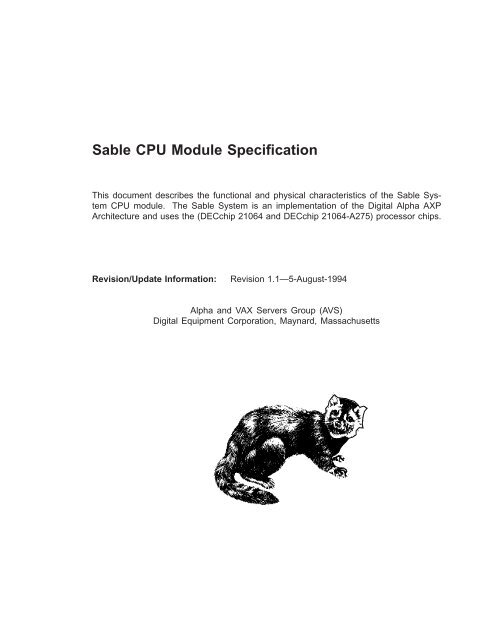
Sable CPU Module Specification
Sable CPU Module Specification
Sable CPU Module Specification

You also want an ePaper? Increase the reach of your titles
YUMPU automatically turns print PDFs into web optimized ePapers that Google loves.
<strong>Sable</strong> <strong>CPU</strong> <strong>Module</strong> <strong>Specification</strong><br />
This document describes the functional and physical characteristics of the <strong>Sable</strong> System<br />
<strong>CPU</strong> module. The <strong>Sable</strong> System is an implementation of the Digital Alpha AXP<br />
Architecture and uses the (DECchip 21064 and DECchip 21064-A275) processor chips.<br />
Revision/Update Information: Revision 1.1—5-August-1994<br />
KURT M. THALLER (TBONE::THALLER, 223-4599)<br />
Alpha and VAX Servers Group (AVS)<br />
Digital Equipment Corporation, Maynard, Massachusetts
Digital Equipment Corporation makes no representations that the use of its products in the manner described<br />
in this publication will not infringe on existing or future patent rights, nor do the descriptions contained<br />
in this publication imply the granting of licenses to make, use, or sell equipment or software in accordance<br />
with the description.<br />
The information in this document is subject to change without notice and should not be construed as a commitment<br />
by Digital Equipment Corporation.<br />
Digital Equipment Corporation assumes no responsibility for any errors that may appear in this document.<br />
The software, if any, described in this document is furnished under a license and may be used or copied only<br />
in accordance with the terms of such license. No responsibility is assumed for the use or reliability of software<br />
or equipment that is not supplied by Digital Equipment Corporation or its affiliated companies.<br />
Copyright © 1990−1994 by Digital Equipment Corporation.<br />
All Rights Reserved.<br />
Printed in U.S.A.<br />
The following are trademarks of Digital Equipment Corporation: AlphaServer, DEC LANcontroller,<br />
OpenVMS, StorageWorks, VAX, and the DIGITAL logo.<br />
MEMORY CHANNEL is a trademark of Encore Computer Corporation.<br />
FCC NOTICE: The equipment described in this manual generates, uses, and may emit radio frequency energy.<br />
The equipment has been type tested and found to comply with the limits for a Class A computing device<br />
pursuant to Subpart J of Part 15 of FCC Rules, which are designed to provide reasonable protection<br />
against such radio frequency interference when operated in a commercial environment. Operation of this<br />
equipment in a residential area may cause interference, in which case the user at his own expense may be<br />
required to take measures to correct the interference.
CONTENTS<br />
Preface ........................................................ v<br />
Chapter 1 <strong>CPU</strong> MODULE COMPONENTS AND FEATURES .......... 1<br />
1.1 The 21064 <strong>CPU</strong> Chip ........................................... 4<br />
1.2 The Alpha AXP Architecture . . ................................... 5<br />
Chapter 2 <strong>CPU</strong> MODULE VARIATIONS ............................. 7<br />
2.1 Form Factors ................................................. 7<br />
Chapter 3 FUNCTIONS LOCATED ON THE DECCHIP 21064 ......... 9<br />
3.1 21064 Chip Features . ........................................... 9<br />
3.1.1 I-box Internal Processor Registers ............................... 11<br />
3.1.2 Branch Prediction Logic . . . ................................... 11<br />
3.1.3 Instruction Translation Buffers (ITBs) . .......................... 12<br />
3.1.4 Interrupt Logic . . ........................................... 13<br />
3.1.5 Performance Counters ........................................ 14<br />
3.1.6 Translation Buffer Tag Register (TB_TAG) ........................ 16<br />
3.1.7 Instruction Translation Buffer Page Table Entry Register (ITB_PTE) . . . . 18<br />
3.1.8 Instruction Cache Control and Status Register (ICCSR) .............. 19<br />
3.1.9 Instruction Translation BUffer Page Table Entry Temporary<br />
Register(ITB_PTE_TEMP) .................................... 21<br />
3.1.10 Exception Address Register (EXC_ADDR) ........................ 21<br />
3.1.11 Serial Line Clear Register (SL_CLR) . . .......................... 23<br />
3.1.12 Serial Line Receive Register (SL_RCV) .......................... 23<br />
3.1.13 Instruction Translation Buffer Zap Register (ITBZAP) .............. 24<br />
3.1.14 Instruction Translation Buffer ASM Register (ITBASM) . . .......... 24<br />
3.1.15 Instruction Translation Buffer IS Register (ITBIS) ................. 24<br />
3.1.16 Processor Status (PS) ....................................... 25<br />
3.1.17 Exception Summary Register (EXC_SUM) ....................... 26<br />
3.1.18 Privileged Architecture Library Base Register (PAL_BASE) .......... 28<br />
3.1.19 Hardware Interrupt Request Register (HIRR) . . .................. 29<br />
3.1.20 Software Interrupt Request Register (SIRR) . . . .................. 31<br />
3.1.21 Asynchronous Trap Request Register (ASTRR) . . .................. 32<br />
3.1.22 Hardware Interrupt Enable Register (HIER) . . . .................. 33<br />
3.1.23 Software Interrupt Enable Register (SIER) ...................... 34<br />
3.1.24 Asynchronous System Trap Enable Register (ASTER) .............. 35<br />
3.1.25 Serial Line Transmit (SL_XMIT) .............................. 36<br />
3.2 Ebox ........................................................ 37<br />
3.3 Abox ........................................................ 37<br />
iii
iv<br />
3.3.1 Abox IPRs ................................................. 37<br />
3.3.2 Translation Buffer Control Register (TB_CTL) . . . .................. 38<br />
3.3.3 Data Translation Buffer Page Table Entry Register (DTB_PTE) ....... 39<br />
3.3.4 Data Translation Buffer Page Table Entry Temporary Register<br />
(DTB_PTE_TEMP) .......................................... 40<br />
3.3.5 Memory Management Control and Status Register (MM_CSR) ........ 41<br />
3.3.6 Virtual Address Register (VA) .................................. 41<br />
3.3.7 Data Translation Buffer Zap Register (DTBZAP) . .................. 41<br />
3.3.8 Data Translation Buffer ASM Register (DTBASM) ................. 42<br />
3.3.9 Data Translation Buffer Invalidate Signal Register (DTBIS) .......... 42<br />
3.3.10 Flush Instruction Cache Register (FLUSH_IC) . .................. 42<br />
3.3.11 Flush Instruction Cache ASM Register (FLUSH_IC_ASM) . .......... 42<br />
3.3.12 A-box Control Register (ABOX_CTL) . .......................... 42<br />
3.3.13 Alternative Processor Mode Register (ALT_MODE) ................ 46<br />
3.3.14 Cycle Counter Register (CC) .................................. 46<br />
3.3.15 Cycle Counter Control Register (CC_CTL) ....................... 46<br />
3.3.16 Bus Interface Unit Control Register (BIU_CTL) . .................. 46<br />
3.3.17 Data Translation Buffer (DTB) ................................ 53<br />
3.3.18 Bus Interface Unit (BIU) . . ................................... 54<br />
3.3.19 Load Silos ................................................ 54<br />
3.3.20 Write Buffer ............................................... 55<br />
3.4 Fbox ........................................................ 56<br />
3.5 21064 IEEE Floating Point Conformance . . .......................... 57<br />
3.6 Cache Organization . ........................................... 59<br />
3.6.1 Data Cache (Dcache) ......................................... 59<br />
3.6.2 Instruction Cache (Icache) . . ................................... 59<br />
3.7 Pipeline Organization ........................................... 59<br />
3.7.1 Static and Dynamic Stages . ................................... 61<br />
3.7.2 Aborts . ................................................... 61<br />
3.7.3 Non-Issue Conditions ......................................... 63<br />
3.8 Scheduling and Issuing Rules . . ................................... 63<br />
3.8.1 Instruction Class Definition . ................................... 63<br />
3.8.2 Producer-Consumer Latency ................................... 65<br />
3.8.3 Producer-Producer Latency . ................................... 67<br />
3.8.4 Instruction Issue Rules ....................................... 67<br />
3.8.5 Dual Issue Table . ........................................... 68<br />
3.9 PALcode . . ................................................... 69<br />
3.9.1 Required PALcode Instructions ................................. 70<br />
3.9.2 Architecturally Reserved PALcode Instructions . . . .................. 70<br />
3.9.3 PAL_TEMPs ............................................... 70<br />
3.9.4 Data Cache Status Register (C_STAT) . .......................... 70<br />
3.9.5 DECchip 21064-A275 Data Cache Status Register (C_STAT) .......... 71
3.9.6 Data Cache Address Register (DC_ADDR) ........................ 73<br />
3.9.7 Bus Interface Unit Status Register (BIU_STAT) . .................. 74<br />
3.9.8 Bus Interface Unit Address Register (BIU_ADDR) .................. 75<br />
3.9.9 Fill Address Register (FILL_ADDR) . . . .......................... 77<br />
3.9.10 Fill Syndrome Register (FILL_SYNDROME) . . . .................. 78<br />
3.9.11 Backup Cache Tag Register (BC_TAG) . .......................... 79<br />
3.9.12 EDC Error Correction ....................................... 81<br />
Chapter 4 FUNCTIONS LOCATED ELSEWHERE ON THE <strong>CPU</strong><br />
MODULE ...................................................... 83<br />
4.1 Back-up Cache (B-Cache) ........................................ 83<br />
4.1.1 Control Store ............................................... 83<br />
4.1.2 Tag Store .................................................. 84<br />
4.1.3 Data Store ................................................. 84<br />
4.1.4 B-Cache Control Register Definitions . . .......................... 85<br />
4.1.4.1 CSR Space . . . ........................................... 85<br />
4.1.4.2 B-Cache Control Register - CSR0 . . . .......................... 86<br />
4.1.4.3 B-Cache Correctable Error Register - CSR1 . . . .................. 92<br />
4.1.4.4 B-Cache Correctable Error Address Register - CSR2 .............. 95<br />
4.1.4.5 B-Cache Uncorrectable Error Register - CSR3 . .................. 97<br />
4.1.4.6 B-Cache Uncorrectable Error Address Register - CSR4 . . .......... 100<br />
4.1.5 Back-up Cache Cycle Time . ................................... 101<br />
4.1.5.1 The 21064 Cycles ......................................... 102<br />
4.1.5.2 System-bus Cycles ........................................ 102<br />
4.2 Cache Block Merge Buffer ....................................... 102<br />
4.3 Duplicate Primary Data Cache Tag Store . . .......................... 103<br />
4.3.1 Duplicate Tag Error Register - CSR5 . . . .......................... 105<br />
4.4 Lack of Duplicate Primary Instruction Cache Tag Store ................. 106<br />
4.5 Lack of Cache Block Prefetch . . ................................... 107<br />
4.6 Data Integrity ................................................. 107<br />
4.7 System-bus Interface ........................................... 107<br />
4.7.1 System-bus Control Register - CSR6 . . . .......................... 108<br />
4.7.2 System-bus Error Register - CSR7 .............................. 111<br />
4.7.3 System-bus Error Address Low Register - CSR8 . . .................. 117<br />
4.7.4 System-bus Error Address High Register - CSR9 . .................. 118<br />
4.8 Multiprocessor Configuration CSR Definitions ........................ 121<br />
4.8.1 Processor Mailbox Register - CSR10 . . . .......................... 121<br />
4.8.2 Interprocessor Interrupt Request Register - CSR11 .................. 122<br />
4.9 System Interrupt Clear Register - CSR12 . . .......................... 123<br />
4.10 Address Lock Register - CSR13 .................................. 125<br />
v
4.11 Miss Address Register - CSR14 ................................... 127<br />
4.11.1 C4 Revision Register - CSR15 ................................. 128<br />
4.12 Interval Timer ............................................... 130<br />
4.13 D-bus . . . ................................................... 131<br />
4.14 System-bus Arbiter . ........................................... 133<br />
4.15 System-bus CRESET L Generation ................................ 136<br />
4.15.1 <strong>Sable</strong> <strong>CPU</strong> Non-Volatile EEPROM .............................. 137<br />
Chapter 5 <strong>CPU</strong> MODULE TRANSACTIONS ......................... 143<br />
5.1 Processor Transactions .......................................... 143<br />
5.1.1 21064 Processor TRANSACTIONS .............................. 146<br />
5.1.1.1 FAST EXTERNAL CACHE READ HIT ........................ 146<br />
5.1.1.2 FAST EXTERNAL CACHE WRITE HIT ....................... 147<br />
5.1.1.3 READ_BLOCK TRANSACTION .............................. 148<br />
5.1.1.4 WRITE_BLOCK .......................................... 150<br />
5.1.1.5 LDxL TRANSACTION . . ................................... 152<br />
5.1.1.6 StxC TRANSACTION . . . ................................... 152<br />
5.1.1.7 BARRIER TRANSACTION .................................. 153<br />
5.1.1.8 FETCH TRANSACTION ................................... 153<br />
5.1.1.9 FETCHM TRANSACTION .................................. 154<br />
5.1.2 Cacheable vs Non-Cacheable vs Allocate-Invalid . .................. 155<br />
5.2 System-bus Transactions ........................................ 156<br />
5.2.1 <strong>CPU</strong> as Commander ......................................... 157<br />
5.2.2 <strong>CPU</strong> as Bystander ........................................... 157<br />
5.2.3 <strong>CPU</strong> as Responder ........................................... 157<br />
5.3 Control Flow of <strong>CPU</strong> <strong>Module</strong> Transactions . .......................... 158<br />
5.3.1 Processor Initiated ........................................... 158<br />
5.3.2 System-bus Initiated ......................................... 162<br />
Chapter 6 CACHE INVALIDATE MANAGEMENT .................... 165<br />
6.1 Processor Caused Invalidates . . ................................... 165<br />
6.2 C-bus Caused Invalidates ........................................ 165<br />
Chapter 7 EXCEPTIONS AND INTERRUPTS ........................ 167<br />
vi<br />
7.1 Processor Generated . ........................................... 167
7.1.1 Exception Handling .......................................... 168<br />
7.1.1.1 PAL Priority Level ........................................ 169<br />
7.1.1.2 PALcode 0020 Entry Characteristics .......................... 169<br />
7.1.1.3 PAL Routine Behavior . . ................................... 169<br />
7.1.1.3.1 B-Cache Tag Parity Error ................................ 169<br />
7.1.1.3.2 B-Cache Tag Control Parity Error .......................... 170<br />
7.1.1.3.3 B-Cache Data Single Bit EDC Error ........................ 170<br />
7.1.1.3.4 B-Cache Data Uncorrectable EDC Error . . . .................. 170<br />
7.1.1.3.5 B-Cache Data Single Bit EDC Error ........................ 171<br />
7.1.1.3.6 B-Cache Data Uncorrectable EDC Error . . . .................. 171<br />
7.1.1.3.7 21064 Data bus Single Bit EDC Error ....................... 171<br />
7.1.1.3.8 21064 Data bus Uncorrectable EDC Error . .................. 171<br />
7.1.1.3.9 B-Cache Tag or Tag Control Parity Error . . .................. 172<br />
7.1.1.3.10 Cobra-bus Parity Error ................................. 172<br />
7.1.1.3.11 Invalid Cobra-bus Address ............................... 172<br />
7.1.1.3.12 Other <strong>CPU</strong> Errors . . ................................... 173<br />
7.1.1.3.13 Main Memory Uncorrectable EDC Errors . .................. 173<br />
7.2 Non-processor Generated ........................................ 173<br />
7.2.1 Interrupt Handling .......................................... 173<br />
7.2.1.1 PAL Priority Level ........................................ 174<br />
7.2.1.2 PALcode 00E0 Entry Characteristics .......................... 174<br />
7.2.1.3 Hardware 0 - Hardware Error ............................... 175<br />
7.2.1.4 Hardware 1 - Local I/O . . ................................... 177<br />
7.2.1.5 Hardware 3 - Interprocessor ................................. 177<br />
7.2.1.6 Hardware 4 - Interval Timer ................................ 177<br />
7.2.1.7 Hardware 5 - System Events ................................ 177<br />
7.2.1.8 Software X . . . ........................................... 178<br />
7.2.1.9 Serial Line . . . ........................................... 178<br />
7.2.1.10 Performance Counter X ................................... 178<br />
7.2.1.11 Asynchronous System Trap ................................. 178<br />
Chapter 8 FAULT MANAGEMENT/ERROR RECOVERY .............. 179<br />
8.1 Processor Errors ............................................... 179<br />
8.2 B-Cache Errors ................................................ 179<br />
8.2.1 Tag and Tag Control Store Parity Errors .......................... 179<br />
8.2.2 Data Store EDC Errors ....................................... 181<br />
8.2.2.1 Correctable . . . ........................................... 181<br />
8.2.2.2 Uncorrectable . ........................................... 183<br />
8.3 Duplicate P-Cache Tag Store Parity Errors .......................... 186<br />
8.4 System-bus Errors . . ........................................... 186<br />
8.4.1 C/A Parity Error . ........................................... 186<br />
8.4.2 Data Parity Error ........................................... 187<br />
vii
8.4.3 Invalid Address - Bus Time-out ................................. 187<br />
8.5 I/O Subsystem Errors ........................................... 188<br />
8.6 C_ERR L Assertion . . ........................................... 188<br />
Chapter 9 <strong>CPU</strong> POWERUP AND INITIALIZATION ................... 189<br />
9.1 Processor Initialization .......................................... 189<br />
9.1.1 Internal Processor Registers ................................... 189<br />
9.1.2 Internal JSR stack ........................................... 189<br />
9.2 B-Cache Initialization ........................................... 189<br />
9.2.1 LDQ Data Format - BCC ENABLE B-CACHE INIT Set .............. 190<br />
9.3 Duplicate Tag Store Initialization .................................. 191<br />
9.4 System-bus Interface Initialization ................................. 191<br />
9.5 <strong>CPU</strong> clocks and reset ........................................... 191<br />
9.6 Power-up Sequence . . ........................................... 191<br />
9.7 Powering Up with Bad Main Memory ............................... 192<br />
Chapter 10 OVERVIEW OF THE <strong>CPU</strong> TESTABILITY FEATURES ...... 193<br />
10.1 Bus Verification ............................................... 193<br />
10.1.1 Address .................................................. 193<br />
10.1.2 Data . . ................................................... 193<br />
10.2 C4 EDC Generators ........................................... 193<br />
10.3 C4 EDC Checkers . . ........................................... 194<br />
10.4 DECchip 21064 EDC Checkers ................................... 194<br />
10.5 DECchip 21064 EDC Generators ................................. 194<br />
10.6 C4 Cobra-bus Probe Predicted Tag Parity Generator .................. 194<br />
10.7 B-Cache Data Store Verification .................................. 194<br />
10.8 B-Cache Tag/Control Store Verification . . . .......................... 194<br />
10.9 Performance Counters ......................................... 195<br />
10.10 Brain Dead <strong>Module</strong> Errors . . ................................... 195<br />
Chapter 11 PHYSICAL AND ELECTRICAL CHARACTERISTICS ...... 197<br />
viii<br />
11.1 <strong>CPU</strong> <strong>Module</strong> Physical <strong>Specification</strong> ................................ 197<br />
11.2 SABLE <strong>CPU</strong> CONNECTOR PINNING . . . .......................... 197<br />
11.3 <strong>CPU</strong> <strong>Module</strong> Max DC Power Requirement .......................... 203
11.4 Environmental <strong>Specification</strong>s - Class B modified . . . .................. 203<br />
11.4.1 Temperature . . . ........................................... 203<br />
11.4.1.1 Storage ................................................ 203<br />
11.4.1.2 Operating . . . ........................................... 203<br />
11.4.2 Relative Humidity .......................................... 203<br />
11.4.2.1 Storage ................................................ 204<br />
11.4.2.2 Operating . . . ........................................... 204<br />
11.4.3 Altitude .................................................. 204<br />
11.4.3.1 Storage ................................................ 204<br />
11.4.3.2 Operating Altitude ....................................... 204<br />
11.4.4 Airflow ................................................... 204<br />
11.4.5 Contamination . . ........................................... 204<br />
11.4.6 Mean Time Between Failure (MTBF) Rate ....................... 204<br />
11.4.7 Electrical Characteristics . . ................................... 204<br />
11.4.7.1 AC References ........................................... 204<br />
11.4.8 Clock Description ........................................... 204<br />
11.4.9 AC and DC Characteristics ................................... 208<br />
Appendix A ALPHA ARCHITECTURE OPTIONS SUPPORTED ....... 211<br />
Appendix B SABLE <strong>CPU</strong> MODULE REGISTER REFERENCE GUIDE<br />
............................................................... 213<br />
Appendix C COBRA SPECIFIC ( PRIVILEGED ARCHITECTURE<br />
LIBRARY CODE ) PALCODE .................................... 223<br />
C.1 Introduction .................................................. 223<br />
C.2 PAL Environment . . ........................................... 223<br />
C.3 Special PAL Instructions ........................................ 224<br />
C.3.1 HW_MFPR and HW_MTPR ................................... 225<br />
C.3.2 HW_LD and HW_ST ......................................... 227<br />
C.3.3 HW_REI .................................................. 228<br />
C.4 PAL Entry Points . . . ........................................... 228<br />
C.5 General PALmode Restrictions ................................... 231<br />
C.5.1 21064 PAL Restrictions ....................................... 231<br />
C.5.2 21064 Specific PALmode Restrictions . .......................... 234<br />
C.6 Powerup . . ................................................... 235<br />
C.7 TB Miss Flows ................................................ 237<br />
C.7.1 ITB Miss .................................................. 237<br />
C.7.2 DTB Miss ................................................. 238<br />
C.8 Error Flows .................................................. 239<br />
ix
C.8.1 21064 Error Flows .......................................... 239<br />
C.8.1.1 EDC Error Handling . . . ................................... 239<br />
C.8.1.1.1 Single Bit I-stream EDC error . . .......................... 239<br />
C.8.1.1.2 Single Bit D-stream EDC error . . .......................... 240<br />
C.8.1.1.3 Double Bit I-stream EDC error . . .......................... 240<br />
C.8.1.1.4 Double Bit D-stream EDC error . .......................... 240<br />
C.8.1.2 BIU: tag address parity error ................................ 241<br />
C.8.1.3 BIU: tag control parity error ................................ 241<br />
C.8.1.4 BIU: system transaction terminated with CACK_HERR . .......... 241<br />
C.8.2 Response to Multiple Errors ................................... 241<br />
Appendix D REVISION HISTORY .................................. 243<br />
INDEX<br />
EXAMPLES<br />
1 Update vs Invalidate Algorithm ................................ 104<br />
FIGURES<br />
1 <strong>Sable</strong> <strong>CPU</strong> <strong>Module</strong> Block Diagram .............................. 2<br />
2 C4 Chip Block Diagram ....................................... 3<br />
3 21064 <strong>CPU</strong> Chip Block Diagram ................................ 4<br />
4 <strong>CPU</strong> Form Factors .......................................... 8<br />
5 TB_TAG_FIG ............................................... 17<br />
6 ITB_PTE .................................................. 18<br />
7 ICCSR . ................................................... 19<br />
8 ITB_PTE_TEMP . ........................................... 21<br />
9 EXC_ADDR ................................................ 22<br />
10 SL_CLR ................................................... 23<br />
11 SL_RCV ................................................... 24<br />
12 PS ....................................................... 25<br />
13 EXC_SUM ................................................. 26<br />
14 PAL_BASE ................................................ 28<br />
15 HIRR . . ................................................... 29<br />
16 SIRR . . ................................................... 31<br />
17 ASTRR ................................................... 32<br />
18 HIER . . ................................................... 33<br />
19 SIER . . ................................................... 34<br />
20 ASTER ................................................... 35<br />
21 SL_XMIT .................................................. 36<br />
22 TB_CTL_FIG ............................................... 38<br />
23 DTB_PTE ................................................. 39<br />
24 DTB_PTE_TEMP ........................................... 40<br />
x
25 MM_CSR .................................................. 41<br />
26 DECchip 21064 ABOX_CTL ................................... 43<br />
27 DECchip 21064-A275 ABOX_CTL ............................... 44<br />
28 ALT_MODE ................................................ 46<br />
29 BIU Control Register (BIU_CTL) ............................... 47<br />
30 DECchip 21064-A275 BIU Control Register (EV45_BIU_CTL) ......... 50<br />
31 Integer Operate Pipeline . . . ................................... 60<br />
32 Memory Reference Pipeline . ................................... 60<br />
33 Floating Point Operate Pipeline ................................ 61<br />
34 Producer-Consumer Latency Matrix . . . .......................... 66<br />
35 DECchip 21064 C_STAT . . . ................................... 71<br />
36 DECchip 21064-A275 C_STAT .................................. 71<br />
37 BIU_STAT ................................................. 74<br />
38 Fill Syndrome . . . ........................................... 78<br />
39 BC_TAG .................................................. 80<br />
40 Back-up Cache Entry ........................................ 83<br />
41 B-Cache Control Register (BCC) ................................ 87<br />
42 B-Cache Correctable Error Register (BCCE) ....................... 92<br />
43 B-Cache Correctable Error Address Register (BCCEA) ............... 95<br />
44 B-Cache Uncorrectable Error Register (BCUE) . . . .................. 97<br />
45 B-Cache Uncorrectable Error Address Register (BCUEA) . . . .......... 100<br />
46 Duplicate Tag Error Register (DTER) . . .......................... 105<br />
47 System-bus Control Register (CBCTL) . .......................... 108<br />
48 System-bus Error Register (CBE) ............................... 112<br />
49 System-bus Error Address Low Register (CBEAL) .................. 117<br />
50 System-bus Error Address High Register (CBEAH) ................. 118<br />
51 Processor Mailbox Register (PMBX) . . . .......................... 121<br />
52 Interprocessor Interrupt Request Register (IPIR) . .................. 122<br />
53 System Interrupt Clear Register (SIC) . .......................... 123<br />
54 Address Lock Register (ADLK) ................................. 125<br />
55 Miss Address Register Low (MADRL) . . .......................... 127<br />
56 C4 Revision Register (CRR) . ................................... 128<br />
57 The 21064 Serial Load Data Format . . . .......................... 131<br />
58 Granting Order . . ........................................... 135<br />
59 FAST EXTERNAL CACHE READ HIT . .......................... 147<br />
60 FAST EXTERNAL CACHE WRITE HIT .......................... 148<br />
61 READ BLOCK TRANSACTION ................................ 149<br />
62 WRITE BLOCK . . ........................................... 151<br />
63 BARRIER TRANSACTION . ................................... 153<br />
64 FETCH TRANSACTION . . . ................................... 154<br />
65 Address Space Map .......................................... 156<br />
66 LDQ Data Format (LDQ_DF) .................................. 190<br />
67 System backplane clocks . . . ................................... 206<br />
68 module clocks . . . ........................................... 207<br />
69 <strong>Module</strong> Layup (reference) . . ................................... 210<br />
xi
70 B-Cache Control Register (BCC-CSR0, offset = 0000) ................ 214<br />
71 B-Cache Correctable Error (BCCE-CSR1, offset = 0020) .............. 215<br />
72 B-Cache Correctable Error Address (BCCEA-CSR2, offset = 0040) ...... 215<br />
73 B-Cache Uncorrectable Error (BCUE-CSR3, offset = 0060) . . .......... 216<br />
74 B-Cache Uncorrectable Error Address (BCUEA-CSR4, offset = 0080) . . . . 216<br />
75 Duplicate Tag Error Register (DTER-CSR5, offset = 00A0) . . .......... 217<br />
76 Cobra-bus Control Register (CBCTL-CSR6, offset = 00C0) . . .......... 218<br />
77 Cobra-bus Error Register (CBE-CSR7, offset = 00E0) ................ 219<br />
78 Cobra-bus Error Address Low (CBEAL-CSR8, offset = 0100) .......... 220<br />
79 Cobra-bus Error Address High (CBEAH-CSR9, offset = 0120) ......... 220<br />
80 Processor Mailbox (PMBX-CSR10, offset = 0140) . .................. 220<br />
81 Interprocessor Interrupt Request (IPIR-CSR11, offset = 0160) ......... 221<br />
82 System Interrupt Clear Register (SIC-CSR12, offset = 0180) .......... 221<br />
83 Address Lock Register (ADLK-CSR13, offset = 01A0) ................ 221<br />
84 Miss Address Register Low (MADRL-CSR14, offset = 01C0) . .......... 222<br />
85 C4 Revision Register (CRR-CSR15, offset = 01E0) .................. 222<br />
TABLES<br />
1 <strong>CPU</strong> <strong>Module</strong>s Variations . . . ................................... 7<br />
2 Latencies for Single and Double Precision Divide Instructions ......... 10<br />
3 Performance Counter 0 Input Selection . .......................... 15<br />
4 Performance Counter 1 Input Selection . .......................... 16<br />
5 ICCSR . ................................................... 19<br />
6 BHE,BPE Branch Prediction Selection . .......................... 20<br />
7 SL_CLR ................................................... 23<br />
8 EXC_SUM ................................................. 27<br />
9 HIRR . . ................................................... 29<br />
10 MM_CSR .................................................. 41<br />
11 Abox Control Register ........................................ 45<br />
12 ALT Mode ................................................. 46<br />
13 BIU Control Register Description ............................... 47<br />
14 DECchip 21064-A275 BIU Control Register Description .............. 50<br />
15 BC_SIZE .................................................. 53<br />
16 BC_PA_DIS ................................................ 53<br />
17 BIU_CTL Initialization Values ................................. 53<br />
18 Producer-Consumer Classes ................................... 64<br />
19 Opcode Summary (with Instruction Issue Bus) . . . .................. 69<br />
20 Required PALcode Instructions ................................. 70<br />
21 Instructions Specific to the 21064 ............................... 70<br />
22 DECchip 21064 Cache Status Register . .......................... 71<br />
23 DECchip 21064-A275 Cache Status Register ....................... 72<br />
24 BIUSTAT ................................................. 75<br />
25 Syndromes for Single-Bit Errors ................................ 78<br />
26 ......................................................... 84<br />
xii
27 Base Addresses for CSRs . . . ................................... 85<br />
28 B-Cache Control Register Description . . .......................... 88<br />
29 B-Cache Correctable Error Register Description . . .................. 92<br />
30 B-Cache Correctable Error Address Register Description . . . .......... 95<br />
31 B-Cache Uncorrectable Error Register Description .................. 98<br />
32 B-Cache Uncorrectable Error Address Register Description . .......... 100<br />
33 The 21064 B-Cache cycle times ................................. 102<br />
34 System-bus B-Cache Access Time ............................... 102<br />
35 Duplicate Tag Error Register Description ......................... 105<br />
36 Data Integrity Reference . . ................................... 107<br />
37 System-bus Control Register Description ......................... 109<br />
38 System-bus Error Register Description . .......................... 113<br />
39 System-bus Error Address Low Register Description ................ 117<br />
40 System-bus Error Address High Register Description ................ 118<br />
41 Processor Mailbox Register Description . .......................... 121<br />
42 Interprocessor Interrupt Request Register Description ............... 122<br />
43 System Interrupt Clear Register Description ...................... 123<br />
44 Address Lock Register Description .............................. 125<br />
45 Miss Address Register Low Description .......................... 127<br />
46 C4 Revision Register Description ............................... 128<br />
47 CSR Space ................................................. 130<br />
48 Interval Timer Interrupt Generation . . . .......................... 130<br />
49 D-bus Micro Port Mapping . ................................... 132<br />
50 D-bus Microcontroller Clock Frequency . .......................... 133<br />
51 D-bus Microcontroller System Control Bus Address ................. 133<br />
52 <strong>Sable</strong> Arbitration Latency . . ................................... 136<br />
53 <strong>CPU</strong> I²C Bus EEPROM Field Definitions ......................... 137<br />
54 BIU_CTL Field Description . ................................... 138<br />
56 BIU_CTL Initialization Values ................................. 140<br />
57 <strong>CPU</strong> EEPROM Defaults . . . ................................... 141<br />
58 ......................................................... 141<br />
59 Cycle Request . . . ........................................... 144<br />
60 Cycle Acknowledgment Types .................................. 145<br />
61 Read Data Acknowledgment Types .............................. 145<br />
62 Processor Initiated Transactions ............................... 146<br />
63 System-bus Initiated Transactions .............................. 157<br />
64 Processor Initiated Transactions - Control Flow . . .................. 158<br />
65 System-bus Initiated Transactions - Control Flow . .................. 162<br />
66 Invalidate Management - C-bus Caused .......................... 165<br />
67 General Exception Isolation Matrix .............................. 167<br />
68 Machine Check Isolation Matrix ................................ 168<br />
69 Exception Priority/PAL Offset/SCB Offset/IPL . . . .................. 169<br />
70 Hardware Interrupt Configuration .............................. 173<br />
71 Interrupt Priority/SCB Offset/IPL ............................... 174<br />
72 Tag/Tag Control Error Severity Matrix . .......................... 179<br />
xiii
xiv<br />
73 B-Cache Tag Control or Tag Store Errors ......................... 181<br />
74 B-Cache Data Correctable Errors ............................... 183<br />
75 Uncorrectable Data Store Error Severity Matrix . . .................. 184<br />
76 B-Cache Uncorrectable Errors .................................. 185<br />
77 C/A Parity Errors ........................................... 187<br />
78 Data Parity Errors .......................................... 187<br />
79 LDQ Data Format Description ................................. 191<br />
80 Kernel Survivability Matrix ................................... 195<br />
81 MCA240 J5 ................................................ 197<br />
82 MCA44 J1 ................................................. 200<br />
83 MCA44 J3 ................................................. 201<br />
84 <strong>CPU</strong> Power Requirements . . ................................... 203<br />
85 System bus AC and DC Characteristics .......................... 208<br />
86 HW_MFPR and HW_MTPR Format Description . . .................. 225<br />
87 IPR Access ................................................. 225<br />
88 HW_LD and HW_ST Format Description ......................... 227<br />
89 The HW_REI Format Description ............................... 228<br />
90 PAL Entry Points ........................................... 229<br />
91 D-stream Error PAL Entry Points ............................... 231<br />
92 IPR Reset State . . ........................................... 235<br />
93 Revision History . ........................................... 243
Preface<br />
Scope and Organization of this <strong>Specification</strong><br />
This specification describes the operation of the <strong>Sable</strong> <strong>CPU</strong>. It contains an overview of<br />
the system, the <strong>CPU</strong> module interfaces to the memory and I/O modules and descriptions<br />
of transactions, addressing, signals, interface registers, and electrical specifications.<br />
In addition, the specification contains discussions of error handling, interrupts,<br />
and initialization as well as a description of the PALcode required to provide ALPHA<br />
SRM conformance.<br />
Related Documents<br />
The following documents are related to or were used in the preparation of this document:<br />
• 21064 Processor <strong>Specification</strong><br />
• Alpha System Reference Manual Version 5.0<br />
• Cobra System Bus <strong>Specification</strong><br />
• <strong>Sable</strong> System Spec<br />
• <strong>Sable</strong> I/O module <strong>Specification</strong><br />
• <strong>Sable</strong> Motherboard <strong>Specification</strong><br />
• <strong>Sable</strong> Memory <strong>Specification</strong><br />
• <strong>Sable</strong> PFMS<br />
Terminology and Conventions<br />
Ranges and Extents<br />
Ranges are specified by a pair of numbers separated by a ‘‘..’’ and are inclusive, for<br />
example, a range of integers 0..4 includes the integers 0,1,2,3,and 4.<br />
Extents are specified by a pair of numbers in angle brackets separated by a colon<br />
and are inclusive, for example, bits specify an extent of bits including bits 7,<br />
6, 5, 4, and 3.<br />
Conventions<br />
Physical addresses are expressed as nine hexadecimal digits punctuated with periods<br />
every four digits for readability. (for example, 2.0800.0040(hex))<br />
All numbers are decimal unless otherwise indicated. Where there is ambiguity, numbers<br />
other than decimal are indicated with the name of the base following the number<br />
in parentheses, for example, FF (hex).<br />
Preface v
Copyright © 1993 Digital Equipment Corporation.<br />
Register bits that must both be set are identified as the logical and of these bits (for<br />
example, ). Bits where either bit could be set are identified as the logical or<br />
of these bits (for example, . A range of bits that is either all set or any set is<br />
specified with ‘‘&:’’ or ‘‘ | :’’.<br />
Shaded boxes found in register definitions indicate bit locations that are read and<br />
should be written as zero’s.<br />
Terminology<br />
B-Cache The Back-up Cache memory subsystem including its control machines.<br />
BIU Bus Interface Unit.<br />
BYSTANDER A Cobra-bus node which is not addressed by a current Cobra-bus commander transaction<br />
address.<br />
CACHE LINE A 32 byte contiguous segment of cache memory, which starts at an aligned hexaword<br />
address.<br />
CACHE BLOCK Synonymous with CACHE LINE.<br />
C4 The gate array(s) that contain the Cobra-bus interface, and B-Cache control machines<br />
on the <strong>CPU</strong> module. Each <strong>CPU</strong> module will have two C4 chips which are quadword<br />
slices of the Cobra-bus interface.<br />
Cobra-bus The Cobra System bus, which implements a snooping protocol, refer to the Cobra<br />
System Bus <strong>Specification</strong> for further details.<br />
CLEAN With reference to a cache block in the cache of a Cobra-bus node, the cache block is<br />
valid but has not been written so it is exactly the same as the contents in the system<br />
memory.<br />
COMMAND A field of the Cobra-bus address and command cycle (cycle 1) which encodes the<br />
transaction type.<br />
COMMANDER A Cobra-bus node which participates in arbitration and initiates transactions.<br />
CONDITIONAL IN- Invalidation of a cached location based upon a set of conditions which are the state of<br />
VALIDATION other caches, or the source of the information causing the invalidate.<br />
CYCLE One clock interval.<br />
D-bus The bus over which the serial ROM data flows after power-up or system restart.<br />
DIRTY With reference to a cache block in the cache of a Cobra-bus node, the cache block is<br />
valid and has been written so it differs from the copy in system memory.<br />
E-bus The 21064 Processor Pin bus.<br />
EV4 Pseudonym for the DECchip 21064 processor chip sometimes used in this Document<br />
EV45 Pseudonym for the DECchip 21064-A275 processor chip sometimes used in this document.<br />
FEPROM The Flash Erasable Programmable Read Only Memory subsystem is found on the<br />
<strong>CPU</strong> module on the A-bus.<br />
HIR Hardware Interrupt Request, a bit field located in the Hardware Interrupt Request<br />
Register of the 21064 processor.<br />
HIT Indicates that a copy of a desired memory location is in a cache.<br />
IPR Internal Processor Register<br />
vi Preface
Copyright © 1993 Digital Equipment Corporation.<br />
Serial Control Bus Based on the Signetics I²C; this bus is used on the Cobra System for intercommunication<br />
of system components as well as error reporting. Refer to the Cobra System<br />
Overview for further details.<br />
Masked Write A write cycle that only updates a subset of nominal data block. (for example, A single<br />
longword update to a cache block)<br />
Memory Like<br />
• Each page frame in the region either exists in its entirety or does not exist in its<br />
entirety; there are no holes within a page frame.<br />
• All locations are read/write.<br />
• A write to a location followed by a read from that location returns precisely the<br />
bits written; all bits act as memory.<br />
• A write to one location does not change any other location.<br />
• Reads have no side effects.<br />
• Longword access granularity is provided.<br />
• Instruction-fetch is supported.<br />
• Load-locked and store-conditional are supported.<br />
MISS Indicates that a copy of a desired memory location is not in a cache.<br />
Non-memory Like Non-memory like regions may have arbitrary behavior. There may be un-implemented<br />
locations or bits anywhere; some locations or bits may be read-only and others writeonly;<br />
address ranges may overlap, such that a write to one location changes the bits<br />
read from a different location; reads may have side effects; longword granularity need<br />
not be supported; instruction-fetch need not be supported; and load-locked and storeconditional<br />
need not be supported.<br />
P-Cache The Primary Cache memory subsystem inside the 21064 processor including its control<br />
machines. The Primary Cache is the cache that is the fastest and closest to the<br />
processor.<br />
PROBE The act of using the current operation address (Cobra-bus or processor) to perform a<br />
cache line lookup to determine if the line is valid and/or must be invalidated, updated,<br />
or returned.<br />
PROCESS FATAL An error that is only fatal to the process(es) whose context the error occurred in.<br />
ERROR<br />
Read-Merge The term Read-Merge indicates that an item is read from a responder/bystander, and<br />
new data is then added to the returned read data. This occurs when a masked write<br />
cycle is requested by the processor, or when unmasked cycles occur and the <strong>CPU</strong> is<br />
configured to allocate on full block write misses.<br />
RESPONDER A Cobra-bus node which accepts or supplies data in response to an address and<br />
command from a Cobra-bus commander.<br />
SHARED With reference to a cache block in the cache of a Cobra-bus node, the cache block is<br />
valid and it is valid in at least one other cache of another Cobra-bus node.<br />
SNOOP For a cached node, the act of monitoring Cobra-bus transactions to determine whether<br />
the node has a copy of a cache line.<br />
Snooping Protocol A cache coherence protocol whereby all nodes on a common system bus monitor all<br />
bus activity. This allows a node to keep it’s copy of a particular datum up to date,<br />
and/or supply data to the bus when it has the newest copy. Refer to the Cobra System<br />
Bus <strong>Specification</strong> and Chapter 5 for further details.<br />
SYSTEM FATAL ER-<br />
ROR<br />
An error that is fatal to system as the error occurred in the context of a system process,<br />
or if the context of an error can not be determined.<br />
TRANSACTION A sequence of cycles which comprise a complete bus operation.<br />
Preface vii
Copyright © 1993 Digital Equipment Corporation.<br />
Unmasked Write A write cycle that updates all locations of a nominal data block.<br />
hexaword update to a cache block)<br />
(for example, A<br />
VICTIM With reference to a cache block in the cache of a Cobra-bus node, the cache block is<br />
valid but is about to be replaced due to a cache block resource conflict.<br />
Victim Processing The process of replacing a VICTIM in the cache.<br />
viii Preface
CHAPTER 1<br />
<strong>CPU</strong> MODULE COMPONENTS AND FEATURES<br />
The <strong>Sable</strong> <strong>CPU</strong> module consists of 11 subsystems listed below:<br />
• DECchip 21064 processor<br />
• Back-up Cache<br />
• Write Merge Buffer<br />
• Duplicate Tag Store<br />
• System-bus interface<br />
• Clock Generator/Distributor<br />
• Arbiter<br />
• Reset Generator<br />
• D-bus serial ROM/Micro<br />
• Clock/Power detect circuitry<br />
• Address Lock to support the Load Lock/Store Conditional construct<br />
Figure 1 shows a high-level block diagram of the <strong>CPU</strong> module.<br />
<strong>CPU</strong> <strong>Module</strong> Components and Features 1
Copyright © 1993 Digital Equipment Corporation.<br />
Figure 1: <strong>Sable</strong> <strong>CPU</strong> <strong>Module</strong> Block Diagram<br />
DATA_A<br />
ADDR<br />
SERIAL<br />
ROM<br />
INV_ADR<br />
ADDR<br />
SERIAL CONTROL BUS<br />
SERIAL CTRL BUS<br />
INTERFACE<br />
TAG_INDEX<br />
TAG_INDEX<br />
CHECK<br />
TAG<br />
21064 <strong>CPU</strong> Chip<br />
B-Cache<br />
TAG STORE<br />
DATA STORE<br />
LW0, LW2<br />
PROC OSC<br />
CLK DETECT<br />
DATA <br />
EVEN SLICE ODD SLICE<br />
System bus interface (SBI)<br />
SYSTEM BUS<br />
2 <strong>CPU</strong> <strong>Module</strong> Components and Features<br />
to Memory module, IO module,<br />
and operator control panel<br />
LW1, LW3<br />
Arbitor<br />
To memory module, and IO module<br />
KN450_BLOCK.DOC<br />
PS @ 55%
Copyright © 1993 Digital Equipment Corporation.<br />
Many of the <strong>CPU</strong> module’s subsystems are incorporated into a single ASIC chip, the<br />
C4 chip, developed in the AVS Engineering Group. These subsystems include the<br />
Write Merge Buffer, Duplicate Tag Store, System-bus interface, and arbitrator, the<br />
Address Lock, and the control machines for B-Cache management and System-bus<br />
Snooping. Figure 2 shows a block diagram of the C4 chip.<br />
Figure 2: C4 Chip Block Diagram<br />
512KB Cache Configuration Shown<br />
TAG <br />
ADDRESS <br />
ADDRESS <br />
ADDRESS <br />
TAG <br />
TAG COMPARITOR<br />
<br />
ECC OR<br />
ECC <br />
DATA OR<br />
DATA <br />
DATA OR<br />
DATA <br />
ECC<br />
GEN/CHECK<br />
TAG PARITY<br />
GEN/CHECK<br />
PRIMARY CACHE<br />
BACK MAP<br />
ADDR<br />
B-CACHE & C-bus<br />
STATUS & CONTROL<br />
REGISTERS<br />
-ADDRESS LOCK<br />
-INTERPROC INTER<br />
-PROC MAILBOX<br />
-NON-MASK INTR<br />
C-BUS<br />
-CONTROL/STATUS<br />
-ERROR<br />
B-CACHE<br />
-CONTROL/STATUS<br />
-ERROR REGS<br />
-TAG STORE ERRORS<br />
WRITE MERGE<br />
BUFFER<br />
WRITE MERGE<br />
BUFFER<br />
HOLD<br />
INVALIDATE<br />
CONTROL<br />
TAG PARITY<br />
PREDICTOR<br />
Cobra-bus<br />
ARBITRATOR<br />
DATA<br />
HOLD<br />
Cache Line<br />
Control<br />
Command Generation<br />
Command Detection<br />
<strong>CPU</strong> <strong>Module</strong> Components and Features 3<br />
ADR<br />
HOLD<br />
C-bus<br />
Interface
Copyright © 1993 Digital Equipment Corporation.<br />
1.1 The 21064 <strong>CPU</strong> Chip<br />
The 21064 <strong>CPU</strong> chip is a 431-pin PGA CMOS-4 chip that contains approximately<br />
2.3 million transistors. The chip is a super-scaler, super-pipelined implementation<br />
of the Digital AXP Architecture. The DECchip 21064-A275 has basically the same<br />
pinning, but is a CMOS-5 chip containing a larger Icache and Dcache. Figure 3<br />
shows a block diagram of the <strong>CPU</strong> chip and Section 1.2 provides a brief description<br />
of the architecture.<br />
Figure 3: 21064 <strong>CPU</strong> Chip Block Diagram<br />
Branch<br />
History Table<br />
EBOX<br />
Multiplier<br />
Adder<br />
Shifter<br />
Logic Box<br />
IRF<br />
Write<br />
Buffer<br />
Address<br />
Generator<br />
ICACHE<br />
IBOX<br />
Prefetcher<br />
Resource<br />
Conflict<br />
PC<br />
Calculation<br />
ITB<br />
Pipeline<br />
Control<br />
ABOX<br />
DCACHE<br />
TAG DATA<br />
DTB<br />
TAG DATA<br />
4 <strong>CPU</strong> <strong>Module</strong> Components and Features<br />
FBOX<br />
Multiplier/<br />
Adder<br />
Divider<br />
FRF<br />
Load<br />
Silo<br />
BIU<br />
Address Bus<br />
Data Bus (128 bits)<br />
External Cache Control<br />
External System Interface<br />
LJ-02107-TI0
1.2 The Alpha AXP Architecture<br />
Copyright © 1993 Digital Equipment Corporation.<br />
The Alpha AXP architecture is a 64-bit load/store RISC architecture designed with<br />
particular emphasis on speed, multiple instruction issue, multiple processors, and<br />
software migration from VAX/VMS and MIPS/ULTRIX.<br />
All registers are 64 bits in length and all operations are performed between 64-bit<br />
registers. All instructions are 32 bits in length. Memory operations are either loads<br />
or stores. All data manipulation is done between registers.<br />
The Alpha AXP architecture supports the following data types:<br />
• 8-, 16-, 32- and 64-bit integers<br />
• IEEE 32-bit and 64-bit floating point formats<br />
• VAX computer 32-bit and 64-bit floating point formats<br />
In the Alpha AXP architecture, instructions interact with each other only by one<br />
instruction writing to a register or memory location and another instruction reading<br />
from that register or memory location. This use of resources makes it easy to build<br />
implementations that issue multiple cycles every <strong>CPU</strong> cycle.<br />
The 21064 uses a set of subroutines, called privileged architecture library code (PALcode),<br />
that is specific to a particular Alpha AXP operating system implementation and<br />
hardware platform. These subroutines provide operating system primitives for context<br />
switching, interrupts, exceptions, and memory management. These subroutines<br />
can be invoked by hardware or CALL_PAL instructions. CALL_PAL instructions use<br />
the function field of the instruction to vector to a specified subroutine. PALcode is<br />
written in standard machine code with some implementation-specific extensions to<br />
provide direct access to low-level hardware functions. PALcode supports optimizations<br />
for multiple operating systems, flexible memory management implementations,<br />
and multi-instruction atomic sequences.<br />
The Alpha AXP architecture does byte shifting and masking with normal 64-bit<br />
register-to-register instructions; it does not include single byte load/store instructions.<br />
The software implementor must determine the precision of arithmetic traps.<br />
For a complete introduction to the Alpha AXP architecture, see the Alpha Architecture<br />
Handbook.<br />
<strong>CPU</strong> <strong>Module</strong> Components and Features 5
CHAPTER 2<br />
<strong>CPU</strong> MODULE VARIATIONS<br />
This specification describes <strong>CPU</strong> modules that are based on the DECchip 21064 and<br />
DECchip 21064-A275 <strong>CPU</strong> chips. The module differ with respect to on-chip cache<br />
size, backup cache size, operational speed, number of system <strong>CPU</strong>’s supported and<br />
form factor. This chapter attempts to define the physical and functional design differences<br />
between the Alpha-based processor modules. Table 1 lists the different <strong>CPU</strong><br />
modules.<br />
Table 1: <strong>CPU</strong> <strong>Module</strong>s Variations<br />
Option<br />
Number<br />
<strong>CPU</strong>/ I/D cache<br />
Chip-Size Frequency<br />
Cycle<br />
Time<br />
Bcache<br />
Size<br />
Cache<br />
Access<br />
B2020-AA DECchip 21064 8K/8K 190 MHZ 5.26 ns 1 MByte 26.3 ns 4<br />
B2024-AA DECchip 21064-A275 16K/16K 275 MHZ 3.64 ns 4 MByte 25.45 ns 4<br />
2.1 Form Factors<br />
<strong>CPU</strong>s<br />
Supported<br />
The processor modules measure approximately 340.6 mm x 228.6 mm and use hidensity<br />
connectors. The Figure 4. form factor for the <strong>CPU</strong> module is shown in<br />
<strong>CPU</strong> <strong>Module</strong> Variations 7
Copyright © 1993 Digital Equipment Corporation.<br />
Figure 4: <strong>CPU</strong> Form Factors<br />
8 <strong>CPU</strong> <strong>Module</strong> Variations<br />
Power MCA<br />
340.6 mm (13.410")<br />
Power<br />
228.6 mm (9.000")<br />
<strong>CPU</strong>_CARD.DOC<br />
PS @ 100%
CHAPTER 3<br />
FUNCTIONS LOCATED ON THE DECCHIP 21064<br />
3.1 21064 Chip Features<br />
The DECchip 21064 microprocessor is the first in a family of chips to implement the<br />
Alpha AXP architecture. The DECchip 21064 is a .75 micron CMOS (.5 micron for<br />
the DECchip 21064-A275) based super-scalar super-pipelined processor using dual<br />
instruction issue. The 21064 chip is packaged in a 431-pin (24x24, 100-mil pin pitch)<br />
PGA package.<br />
The 21064 and associated PALcode implement IEEE single and double precision,<br />
VAX F_floating and G_floating datatypes and supports longword (32-bit) and quadword<br />
(64-bit) integers. Byte (8-bit) and word (16-bit) support is provided by byte<br />
manipulation instructions. Limited hardware support is provided for the VAX D_<br />
floating datatype.<br />
(G_floating and S_floating)<br />
The architecturally optional instructions RCC is also implemented.<br />
Other 21064 features include:<br />
• Peak instruction execution of 380 million operations per second at a 190-MHz<br />
clock rate (275 MHZ for DECchip 21064-A275)<br />
• Flexible external interface supporting a complete range of system sizes and performance<br />
levels while maintaining peak <strong>CPU</strong> execution speed<br />
• Selectable data bus width and speed: 64-bit or 128-bit width, 75 MHz to 18.75<br />
MHz bus speed<br />
• An internal clock generator providing a high-speed chip clock and a pair of programmable<br />
system clocks (<strong>CPU</strong>/2 to <strong>CPU</strong>/8)<br />
• Support for external secondary cache including programmable cache size and<br />
speed<br />
• An on-chip write buffer with four 32-byte entries, with ‘‘byte merging’’ capability.<br />
• An on-chip pipelined floating point unit capable of executing both DEC and IEEE<br />
floating point instructions. The floating point unit can accept a new instruction<br />
every cycle, except for divide instructions. The operate-to-operate latency for all<br />
instructions other than divide is six <strong>CPU</strong> cycles. The latencies for single and<br />
double precision divide instructions are shown in Table 2.<br />
Functions Located on the DECchip 21064 9
Copyright © 1993 Digital Equipment Corporation.<br />
Table 2: Latencies for Single and Double Precision Divide Instructions<br />
DECchip 21064 DECchip 21064-A275<br />
single 34 19<br />
double 64 29<br />
• An on-chip 8K byte for DECchip 21064 (or 16K byte two-way set associative<br />
DECchip 21064-A275) direct mapped, write through physical data cache with a<br />
block size of 32 bytes.<br />
• An on-chip 8K byte for DECchip 21064 and 16K byte for DECchip 21064-A275<br />
direct mapped, read-only physical (managed as a virtual) instruction cache with<br />
a block size of 32 bytes.<br />
• An on-chip demand paged memory management unit which, in conjunction with<br />
properly written PALcode, fully implements the Alpha memory management architecture.<br />
The translation buffer can be used with alternative PALcode to implement<br />
a different page table structure. The memory mangament unit contains<br />
the following:<br />
• A 12-entry I-stream translation buffer with 8 entries for 8K byte pages and<br />
4 entries for 4 MB pages<br />
• A 32-entry D-stream translation buffer with each entry able to map a single<br />
8K, 64K, 512K, or 4 MB page<br />
• A demand page memory management unit<br />
• On-chip parity and ECC support<br />
• 3.3-volt Power supply with interface to 5-volt logic<br />
• An on-chip 8-entry I-stream Translation Buffer for mapping 8KB physical pages<br />
and a 4-entry I-stream Translation Buffer for mapping groups of up to 512 contiguous<br />
8KB pages. A 32-entry D-stream Translation Buffer for mapping 8KB<br />
physical pages, and a 4-entry data stream translation buffer for mapping aligned<br />
groups of 512 contiguous 8KB pages.<br />
• The 21064 will implement a dynamic branch prediction algorithm using a 2KB x<br />
1 bit branch history table. An internal control register bit will be used to select<br />
between these two algorithms.<br />
• The Alpha AXP Architecture includes scaled add instructions that improve the<br />
performance of address calculations for longword and quadword length array<br />
elements. The 21064’s integer execution unit will be changed to support these<br />
instructions.<br />
• Low average cycles per instruction (CPI). The 21064 chip can issue two Alpha<br />
instructions in a single cycle, thereby minimizing the aver CPI. Branch history<br />
tables are also used to minimize the branch latency, further reducing the average<br />
CPI.<br />
• A single-entry stream buffer will be used to prefetch 32-byte instruction cache<br />
blocks.<br />
10 Functions Located on the DECchip 21064
Copyright © 1993 Digital Equipment Corporation.<br />
• A bus interface unit, that contains logic that directly controls one bank of external<br />
cache RAMs, and processes ‘‘easy’’ cycles without any <strong>CPU</strong> module action.<br />
• A serial ROM interface for booting and diagnostics for chip and module level test<br />
support<br />
• A clock generator.<br />
The 21064 <strong>CPU</strong> chip consists of three independent execution units: integer execution<br />
unit (E-box), floating point unit (F-box), and the address generation, memory<br />
management, write buffer and bus interface unit (A-box). Each unit can accept at<br />
most one instruction per cycle, however if code is properly scheduled, this <strong>CPU</strong> chip<br />
can issue two instructions to two independent units in a single cycle. A fourth box,<br />
the (I-box), is the central control unit. It issues instructions, maintains the pipeline,<br />
and performs all of the PC calculations.<br />
3.1.1 I-box Internal Processor Registers<br />
The primary function of the I-box is to issue instructions to the E-box, A-box, and<br />
F-box. The I-box decodes two instructions in parallel and checks that the required<br />
resources are available for both instructions. Section 3.1.6 through Section 3.1.25<br />
describe the I-box internal processor registers. In order to provide those instructions,<br />
the Ibox contains:<br />
• The prefetcher<br />
• PC pipeline<br />
• ITB<br />
• Abort logic<br />
• Register conflict or dirty logic<br />
• Exception logic<br />
The Ibox decodes two instructions in parallel and checks that the required resources<br />
are available for both instructions.<br />
If resources are available then both instructions are issued. See Section 3.8.5 for<br />
details on instructions that can be dual issued.The Ibox does not issue instructions<br />
out of order; if the resources are available for the second instruction, but not for the<br />
first instruction, then the Ibox issues neither. The resources for the first instruction<br />
must be available before the Ibox issues any instructions. If the Ibox issues only<br />
the first of a pair of instructions, the Ibox does not advance another instruction to<br />
attempt dual issue again. Dual issue is only attempted on aligned quadword pairs.<br />
3.1.2 Branch Prediction Logic<br />
The Ibox contains the branch prediction logic. The 21064 offers a choice of branch prediction<br />
strategies selectable through the ICCSR IPR. The Icache records the outcome<br />
of branch instructions in a single history bit provided for each instruction location in<br />
the Icache. This information can be used as the prediction for the next execution of<br />
Functions Located on the DECchip 21064 11
Copyright © 1993 Digital Equipment Corporation.<br />
the branch instruction. The prediction for the first execution of a branch instruction<br />
is based on the sign of the displacement field within the branch instruction itself.<br />
• If the sign bit is negative, the instruction prefetcher predicts the conditional<br />
branches to be taken.<br />
• If the sign is positive, the instruction prefetcher predicts the conditional branches<br />
not to be taken.<br />
• Alternatively, if the history table is disabled, branches can be predicted based on<br />
the sign of the displacement field at all times.<br />
The 21064 provides a four-entry subroutine return stack that is controlled by the hint<br />
bits in the BSR, HW_REI, and jump to subroutine instructions (JMP, JSR, RET, or<br />
JSR_COROUTINE). The chip also provides a means of disabling all branch prediction<br />
hardware.<br />
3.1.3 Instruction Translation Buffers (ITBs)<br />
The Ibox contains two ITBs.<br />
• An eight-entry, fully associative translation buffer that caches recently used<br />
instruction-stream page table entries for 8K byte pages<br />
• A four-entry, fully associative translation buffer that supports the largest granularity<br />
hint option (512 3 8K byte pages) as described in the Alpha Architecture<br />
Handbook.<br />
Both translation buffers use a not-last-used replacement algorithm. They are hereafter<br />
referred to as the small-page and large-page ITBs, respectively.<br />
In addition, the ITB includes support for an extension called the super page, which<br />
can be enabled by the MAP bit in the ICCSR IPR. Super page mappings provide<br />
one-to-one virtual PC [33:13] to physical PC [33:13] translation when virtual address<br />
bits [42:41] = 2. When translating through the super page, the PTE[ASM] bit used<br />
in the Icache is always set. Access to the super page mapping is only allowed while<br />
executing in kernel mode.<br />
PALcode fills and maintains the ITBs. The operating system, through PALcode, is<br />
responsible for ensuring that virtual addresses can only be mapped through a single<br />
ITB entry (in the large page, small page, or super page) at the same time.<br />
The Ibox presents the 43-bit virtual program counter (VPC) to the ITB each cycle<br />
while not executing in PALmode. If the PTE associated with the VPC is cached in<br />
the ITB then the Ibox uses the PFN and protection bits for the page that contains<br />
the VPC to complete the address translation and access checks.<br />
The 21064 ITB supports a single address space number (ASN) via the PTE[ASM]<br />
bit. Each PTE entry in the ITB contains an address space match (ASM) bit. Writes<br />
to the ITBASM IPR invalidate all entries that do not have their ASM bit set. This<br />
provides a simple method of preserving entries that map operating system regions<br />
while invalidating all others.<br />
12 Functions Located on the DECchip 21064
3.1.4 Interrupt Logic<br />
Copyright © 1993 Digital Equipment Corporation.<br />
The 21064 chip supports three sources of interrupts.<br />
• Hardware<br />
There are six level-sensitive hardware interrupts sourced by pins.<br />
• Software<br />
There are fifteen software interrupts sourced by an on-chip IPR (SIRR).<br />
• Asynchronous system trap (AST)<br />
There are four AST interrupts sourced by a second internal IPR (ASTRR).<br />
All interrupts are independently maskable by on-chip enable registers to support a<br />
software controlled mechanism for prioritization. In addition, AST interrupts are<br />
qualified by the current processor mode and the current state of SIER [2].<br />
By providing distinct enable bits for each independent interrupt source, a software<br />
controlled interrupt priority scheme can be implemented by PALcode or the operating<br />
system with maximum flexibility.<br />
For example, the 21064 can support a six-level interrupt priority scheme through<br />
the six hardware interrupt request pins. This is done by defining a distinct state<br />
of the hardware interrupt enable register (HIER) for each interrupt priority level<br />
(IPL). The state of the HIER determines the current interrupt priority. The lowest<br />
interrupt priority level is produced by enabling all six interrupts, for example bits<br />
. The next is produced by enabling bits and so on, to the highest interrupt<br />
priority level that is produced by enabling only bit 6 , and disabling bits . When<br />
all interrupt enable bits are cleared, the processor can not be interrupted from the<br />
hardware interrupt request register (HIRR). Each state, (, , , ,<br />
, ) represents an individual IPL. If these states are the only states allowed<br />
in the HIER, a six-level hardware interrupt priority scheme can be controlled entirely<br />
by PAL software.<br />
The scheme is extensible to provide multiple interrupt sources at the same interrupt<br />
priority level by grouping enable bits. Groups of enable bits must be set and cleared<br />
together to support multiple interrupts of equal priority level. This method reduces<br />
the total available number of distinct levels.<br />
Because enable bits are provided for all hardware, software, and AST interrupt requests,<br />
a priority scheme can span all sources of processor interrupts. The only<br />
exception to this rule is the following restriction on AST interrupt requests:<br />
Four AST interrupts are provided, one for each processor mode. AST interrupt<br />
requests are qualified such that AST requests corresponding to a given mode are<br />
blocked whenever the processor is in a higher mode regardless of the state of<br />
the AST interrupt enable register. In addition, all AST interrupt requests are<br />
qualified in the 21064 with SIER[2].<br />
Functions Located on the DECchip 21064 13
Copyright © 1993 Digital Equipment Corporation.<br />
When the processor receives an interrupt request and that request is enabled, hardware<br />
reports or delivers an interrupt to the exception logic if the processor is not<br />
currently executing PALcode. Before vectoring to the interrupt service PAL dispatch<br />
address, the pipeline is completely drained and all outstanding data cache fills are<br />
completed. The restart address is saved in the Exception Address IPR (EXC_ADDR)<br />
and the processor enters PALmode. The cause of the interrupt may be determined<br />
by examining the state of the interrupt request registers.<br />
NOTE<br />
Hardware interrupt requests are level-sensitive and, therefore, may be removed<br />
before an interrupt is serviced. If they are removed before the interrupt<br />
request register is read, the register will return a zero value.<br />
3.1.5 Performance Counters<br />
The 21064 chip contains a performance recording feature. The implementation of<br />
this feature provides a mechanism to count various hardware events and cause an<br />
interrupt upon counter overflow. Interrupts are triggered six cycles after the event,<br />
and therefore, the exception program counter may not reflect the exact instruction<br />
causing counter overflow. Two counters are provided to allow accurate comparison<br />
of two variables under a potentially non-repeatable experimental condition. Counter<br />
inputs include:<br />
• Issues<br />
• Non-Issues<br />
• Total cycles<br />
• Pipe dry<br />
• Pipe freeze<br />
• Mispredicts and cache misses<br />
• Counts for various instruction classifications<br />
In addition, the 21064 provides one chip pin input to each counter to measure external<br />
events at a rate determined by the selected system clock speed.<br />
They are reset to zero on power-up, but are otherwise never cleared. They are intended<br />
as a means of counting events over a long period of time relative to the event<br />
frequency and therefore provide no means of extracting intermediate counter values.<br />
Because the counters continuously accumulate selected events despite interrupts being<br />
enabled, the first interrupt after selecting a new counter input has an error bound<br />
as large as the selected overflow range.<br />
In addition, some inputs may over count events occurring simultaneously with Dstream<br />
errors which abort the actual event very late in the pipeline. For example,<br />
when counting load instructions, attempts to execute a load resulting in a DTB miss<br />
exception will increment the performance counter after the first aborted execution<br />
attempt and again after the TB fill routine when the load instruction reissues and<br />
completes.<br />
14 Functions Located on the DECchip 21064
Copyright © 1993 Digital Equipment Corporation.<br />
Performance counter interrupts are reported six cycles after the event that caused<br />
the counter to overflow. Additional delay may occur before an interrupt is serviced<br />
if the processor is executing PALcode which always disables interrupts. In either<br />
case, events occurring during the interval between counter overflow and interrupt<br />
service are counted toward the next interrupt. Only in the case of a complete counter<br />
wraparound while interrupts are disabled will an interrupt be missed.<br />
The six cycles before an interrupt is triggered implies that a maximum of 12 instructions<br />
may have completed before the start of the interrupt service routine. When<br />
counting I-Cache misses, no intervening instructions can complete and the exception<br />
PC contains the address of the last I-Cache miss. Branch "mispredictions" allow<br />
a maximum of only 2 instructions to complete before start of the interrupt service<br />
routine.<br />
Table 3: Performance Counter 0 Input Selection<br />
MUX0[3:0] Input Comment<br />
000X Total Issues / 2 Counts total issues divided by 2, e.g dual issue increments count<br />
by 1<br />
001X Pipeline Dry Counts cycles where nothing issued due to lack of valid I-stream<br />
data. Causes include I-Cache fill, misprediction, branch delay<br />
slots and pipeline drain for exception<br />
010X Load Instructions Counts all Load instructions<br />
011X Pipeline Frozen Counts cycles where nothing issued due to resource conflict.<br />
100X Branch Instructions Counts all Branch instructions, conditional, unconditional, any<br />
JSR, HW_REI<br />
1011 PALmode Counts cycles while executing in PALmode<br />
1010 Total cycles Counts total cycles<br />
110X Total Non-issues / 2 Counts total non_issues divided by 2, e.g no issue increments<br />
count by 1<br />
111X PERF_CNT_H Counts external event supplied by pin at selected system clock<br />
cycle interval<br />
Functions Located on the DECchip 21064 15
Copyright © 1993 Digital Equipment Corporation.<br />
Table 4: Performance Counter 1 Input Selection<br />
MUX1[2:0] Input Comment<br />
000 D-Cache miss Counts total D-Cache misses<br />
001 I-Cache miss Counts total I-Cache misses<br />
010 Dual issues Counts cycles of Dual issue<br />
011 Branch Mispredicts Counts both conditional branch mispredictions and JSR or HW_<br />
REI mispredictions. Conditional branch mispredictions cost 4<br />
100 FP Instructions<br />
cycles and others cost 5 cycles of dry pipeline delay.<br />
Counts total floating point operate instructions, i.e no FP branch,<br />
load, store<br />
101 Integer Operate Counts integer operate instructions including LDA,LDAH with<br />
destination other than R31<br />
110 Store Instructions Counts total store instructions<br />
111 PERF_CNT_H Counts external event supplied by pin at selected system clock<br />
cycle interval<br />
3.1.6 Translation Buffer Tag Register (TB_TAG)<br />
The TB_TAG register is a write-only register that holds the tag for the next TB<br />
update operation in either the ITB or DTB. To ensure the integrity of the TB, the<br />
tag is actually written to a temporary register and not transferred to the ITB or<br />
DTB until the ITB_PTE or DTB_PTE register is written. The entry to be written is<br />
chosen at the time of the ITB_PTE or DTB_PTE write operation by a not-last-used<br />
algorithm implemented in hardware.<br />
Writing the ITB_TAG register is only performed while in PALmode regardless of the<br />
state of the HWE bit in the ICCSR IPR.<br />
16 Functions Located on the DECchip 21064
Figure 5: TB_TAG_FIG<br />
6<br />
3<br />
6<br />
3<br />
Small Page Format:<br />
4 4<br />
3 2<br />
Copyright © 1993 Digital Equipment Corporation.<br />
1 1<br />
3 2<br />
IGN VA[42..13] IGN<br />
GH = 11(bin) Format (DTB only):<br />
IGN<br />
4 4<br />
3 2<br />
2 2<br />
2 1<br />
VA[42..22] IGN<br />
0<br />
0<br />
0<br />
0<br />
TB_TAG<br />
Functions Located on the DECchip 21064 17
Copyright © 1993 Digital Equipment Corporation.<br />
3.1.7 Instruction Translation Buffer Page Table Entry Register (ITB_PTE)<br />
The ITB PTE register is a read/write register representing the twelve ITB page table<br />
entries. The first eight provide small page (8K byte) translations while the remaining<br />
four provide large page (4M byte) translations. The entry to be written is chosen by<br />
a not-last-used algorithm implemented in hardware. Writes to the ITB_PTE use the<br />
memory format bit positions as described in the Alpha Architecture Handbook with<br />
the exception that some fields are ignored.<br />
To ensure the integrity of the ITB, the ITB’s tag array is updated simultaneously from<br />
the internal tag register when the ITB_PTE register is written. Reads of the ITB_<br />
PTE require two instructions. First, a read from the ITB_PTE sends the PTE data to<br />
the ITB_PTE_TEMP register, then a second instruction reading from the ITB_PTE_<br />
TEMP register returns the PTE entry to the register file. Reading or writing the<br />
ITB_PTE register increments the TB entry pointer corresponding to the large/small<br />
page selection indicated by the TB_CTL, which allows reading the entire set of ITB_<br />
PTE register entries.<br />
Reading and writing the ITB_PTE register is only performed while in PALmode<br />
regardless of the state of the HWE bit in the ICCSR IPR.<br />
Figure 6: ITB_PTE<br />
6<br />
3<br />
6<br />
3<br />
Write Format:<br />
5<br />
3<br />
5<br />
2<br />
3<br />
2<br />
3<br />
1<br />
U S E K<br />
IGN PFN[33..13] IGN R R R R IGN<br />
E E E E<br />
Read Format:<br />
RAZ<br />
18 Functions Located on the DECchip 21064<br />
3<br />
4<br />
A<br />
S<br />
M<br />
3<br />
3<br />
1<br />
3<br />
1<br />
2<br />
1<br />
2<br />
1<br />
1<br />
1<br />
1<br />
U S E K<br />
PFN[33..13] R R R R<br />
RAZ<br />
E E E E<br />
1<br />
0<br />
1<br />
0<br />
0<br />
9<br />
0<br />
9<br />
0<br />
8<br />
0<br />
8<br />
0<br />
7<br />
0<br />
7<br />
0<br />
6<br />
0<br />
6<br />
0<br />
5<br />
0<br />
5<br />
0<br />
4<br />
A<br />
S<br />
M<br />
0<br />
4<br />
0<br />
3<br />
0<br />
3<br />
0<br />
2<br />
0<br />
1<br />
IGN<br />
0<br />
2<br />
0<br />
1<br />
0<br />
0<br />
0<br />
0<br />
ITB_PTE
3.1.8 Instruction Cache Control and Status Register (ICCSR)<br />
Copyright © 1993 Digital Equipment Corporation.<br />
The ICCSR register contains various Ibox hardware enables. The only architecturally<br />
defined bit in this register is the FPE, floating point enable, which enables floating<br />
point instruction execution. When clear, all floating point instructions generate FEN<br />
exceptions. Most of this register is cleared by hardware at reset. Fields which are<br />
not cleared at reset include ASN, PC0, and PC1.<br />
The HWE bit allows the special PAL instructions to execute in kernel model. This<br />
bit is intended for diagnostics or operating system alternative PAL routines only. It<br />
does not allow access to the ITB registers while not running in PALmode. Therefore,<br />
some PALcode flows may require the PALmode environment to execute properly (e.g.<br />
ITB fill).<br />
Figure 7: ICCSR<br />
6<br />
3<br />
6<br />
3<br />
5<br />
3<br />
Write Format:<br />
5<br />
2<br />
4<br />
7<br />
4<br />
6<br />
4<br />
3<br />
4<br />
2<br />
4<br />
1<br />
4<br />
0<br />
3<br />
9<br />
RES F M H D B J B P PC<br />
PC<br />
MBZ ASN[5:0] [5:2] P A W I H S P I MUX1 MBZ MUX0<br />
E P E E E E P<br />
E<br />
[2:0]<br />
[3:0]<br />
RAZ<br />
Read Format:<br />
3<br />
5<br />
3<br />
4<br />
R<br />
E<br />
S<br />
Table 5: ICCSR<br />
Field Type Description<br />
3<br />
3<br />
2<br />
8<br />
2<br />
7<br />
2<br />
4<br />
RES F M H D B J B<br />
ASN[5:0] [5:2] P A W I H S P<br />
E P E E E E<br />
2<br />
3<br />
2<br />
2<br />
3<br />
8<br />
2<br />
1<br />
3<br />
7<br />
2<br />
0<br />
3<br />
6<br />
1<br />
9<br />
3<br />
5<br />
1<br />
8<br />
3<br />
4<br />
3<br />
3<br />
1<br />
6<br />
3<br />
2<br />
1<br />
5<br />
3<br />
1<br />
PC<br />
MUX1<br />
[2:0]<br />
1<br />
3<br />
1<br />
2<br />
1<br />
2<br />
1<br />
1<br />
1<br />
0<br />
1<br />
0<br />
PC<br />
MUX0<br />
[3:0]<br />
FPE RW,0 If set, floating point instructions can be issued. If clear,floating point instructions<br />
cause FEN exceptions.<br />
HWE RW,0 If set allows the five PALRES instructions to be issued in kernel mode. If<br />
cleared, attempted execution of PALRES instructions while not in PALmode<br />
result in OPCDEC exceptions.<br />
MAP RW,0 If set allows super page I-stream memory mapping of VPC directly to<br />
Physical PC essentially bypassing ITB for VPC addresses containing<br />
VPC=2. Super page mapping is allowed in Kernel mode only. The<br />
ASM bit is always set. If clear, superpage mapping is disabled.<br />
1<br />
7<br />
P<br />
I<br />
P<br />
E<br />
1<br />
4<br />
1<br />
1<br />
0<br />
9<br />
0<br />
9<br />
0<br />
8<br />
0<br />
8<br />
0<br />
7<br />
0<br />
7<br />
0<br />
5<br />
MBZ<br />
0<br />
6<br />
0<br />
4<br />
R<br />
E<br />
S<br />
0<br />
5<br />
RAZ<br />
0<br />
3<br />
P<br />
C<br />
0<br />
0<br />
4<br />
0<br />
2<br />
0<br />
3<br />
0<br />
1<br />
MBZ<br />
Functions Located on the DECchip 21064 19<br />
0<br />
2<br />
P<br />
C<br />
1<br />
0<br />
0<br />
P<br />
C<br />
1<br />
0<br />
1<br />
P<br />
C<br />
0<br />
0<br />
0<br />
R<br />
A<br />
Z<br />
ICCSR
Copyright © 1993 Digital Equipment Corporation.<br />
Table 5 (Cont.): ICCSR<br />
Field Type Description<br />
DI RW,0 If set enables dual issue. If cleared, instructions can only single issue.<br />
BHE RW,0 Used in conjunction with BPE. See table Table 6 for programming information.<br />
JSE RW,0 If set enables the JSR stack to push return addresses. If cleared, JSR stack<br />
is disabled.<br />
BPE RW,0 Used in conjunction with BHE. See table Table 6 for programming information.<br />
PIPE RW,0 If clear causes all hardware interlocked instructions to drain the machine and<br />
waits for the write buffer to empty before issuing the next instruction. Examples<br />
of instructions that do not cause the pipe to drain include HW_MTPR,<br />
HW_REI, conditional branches, and instructions that have a destination register<br />
of R31. If set, pipeline proceeds normally.<br />
PCMUX1 RW,0 See table Table 4 for programming information. Performance counters are<br />
present only in the 21064.<br />
PCMUX0 RW,0 See table Table 3 for programming information. Performance counters are<br />
present only in the 21064.<br />
PC1 RW If clear enables performance counter 1 interrupt request after 2 12 events<br />
counted. If set enables performance counter 1 interrupt request after 2 8<br />
PC0 RW<br />
events counted.<br />
If clear enables performance counter 0 interrupt request after 2 16 events<br />
counted. If set enables performance counter 0 interrupt request after 2 12<br />
ASN RW<br />
events counted.<br />
The Address Space Number field is used in conjunction with the I-Cache in<br />
the 21064 to further qualify cache entries and avoid some cache flushes. The<br />
ASN is written to the I-Cache during fill operations and compared with the<br />
I-stream data on fetch operations. Mismatches invalidate the fetch without<br />
affecting the I-Cache. This function is only present in the 21064.<br />
RES RW,0 The RES state bits are reserved by Digital and should not be used by software.<br />
ICCSR RW,0 When set the performance counters will be enabled and will increment. During<br />
normal operation these bits should be written with 0 to disable the performance<br />
counters.<br />
NOTE<br />
Use of HW_MTPR instruction to update the EXC_ADDR IPR while in native<br />
mode is restricted to values with bit equal to 0. The combination of native<br />
mode and EXC_ADDR equal to one causes UNDEFINED behavior.<br />
Table 6: BHE,BPE Branch Prediction Selection<br />
BPE BHE Prediction<br />
0 X Not Taken<br />
1 0 Sign of Displacement<br />
1 1 Branch History Table<br />
20 Functions Located on the DECchip 21064
Copyright © 1993 Digital Equipment Corporation.<br />
3.1.9 Instruction Translation BUffer Page Table Entry Temporary<br />
Register(ITB_PTE_TEMP)<br />
The ITB_PTE_TEMP register is a read-only holding register for ITB_PTE read data.<br />
Reads of the ITB_PTE require two instructions to return the data to the register<br />
file. The first reads the ITB_PTE register to the ITB_PTE_TEMP register. The<br />
second returns the ITB_PTE_TEMP register to the integer register file. The ITB_<br />
PTE_TEMP register is updated on all ITB accesses, both read and write. A read<br />
of the ITB_PTE to the ITB_PTE_TEMP should be followed closely by a read of the<br />
ITB_PTE_TEMP to the register file.<br />
Reading the ITB_PTE_TEMP register is only performed while in PALmode regardless<br />
of the state of the HWE bit in the ICCSR IPR.<br />
Figure 8: ITB_PTE_TEMP<br />
6<br />
3<br />
3<br />
5<br />
3<br />
4<br />
3<br />
3<br />
A<br />
U S E K<br />
RAZ S PFN[33..13] R R R R RAZ<br />
M<br />
E E E E<br />
3.1.10 Exception Address Register (EXC_ADDR)<br />
1<br />
3<br />
1<br />
2<br />
1<br />
1<br />
1<br />
0<br />
0<br />
9<br />
0<br />
8<br />
0<br />
0<br />
ITB_PTE_TEMP<br />
The EXC_ADDR register is a read/write register used to restart the machine after exceptions<br />
or interrupts. The EXC_ADDR register can be read and written by software<br />
by way of the HW_MTPR instruction as well as being written directly by hardware.<br />
The HW_REI instruction executes a jump to the address contained in the EXC_<br />
ADDR register. The EXC_ADDR register is written by hardware after an exception<br />
to provide a return address for PALcode.<br />
The instruction pointed to by the EXC_ADDR register did not complete execution.<br />
Since the PC is longword aligned, the lsb of the EXC_ADDR register is used to<br />
indicate PALmode to the hardware. When the lsb is clear, the HW_REI instruction<br />
executes a jump to native (non-PAL) mode, enabling address translation.<br />
CALL_PAL exceptions load the EXC_ADDR with the PC of the instruction following<br />
the CALL_PAL. This function allows CALL_PAL service routines to return without<br />
needing to increment the value in the EXC_ADDR register.<br />
This feature, however, requires careful treatment in PALcode. Arithmetic traps and<br />
machine check exceptions can pre-empt CALL_PAL exceptions resulting in an incorrect<br />
value being saved in the EXC_ADDR register. In the cases of an arithmetic<br />
trap or a machine check exception, and only in these cases, EXC_ADDR takes<br />
on special meaning. PALcode servicing these two exceptions should interpret a zero<br />
in EXC_ADDR as indicating that the PC in EXC_ADDR is too large by a<br />
value of 4 bytes and subtract 4 before executing a HW_REI from this address. PALcode<br />
should interpret a one in EXC_ADDR as indicating that the PC in EXC_<br />
Functions Located on the DECchip 21064 21
Copyright © 1993 Digital Equipment Corporation.<br />
ADDR is correct and clear the value of EXC_ADDR. All other PALcode<br />
entry points except reset can expect EXC_ADDR to be zero.<br />
This logic allows the following code sequence to conditionally subtract 4 from the<br />
address in the EXC_ADDR register without use of an additional register. This code<br />
sequence should be present in arithmetic trap and machine check flows only.<br />
HW_MFPR Rx, EXC_ADDR ; read EXC_ADDR into GPR<br />
SUBQ Rx, #2, Rx ; subtract 2 causing borrow if [1]=0<br />
BIC Rx, #2, Rx ; clear [1]<br />
HW_MTPR Rx, EXC_ADDR ; write back to EXC_ADDR<br />
Note that bit 1 is undefined when the EXC_ADDR is read. The actual hardware<br />
ignores this bit, however PALcode must explicitly clear this bit before it pushes the<br />
exception address on the stack.<br />
IPR Format:<br />
Figure 9: EXC_ADDR<br />
6<br />
3<br />
PC[63..2]<br />
22 Functions Located on the DECchip 21064<br />
0<br />
2<br />
0<br />
1<br />
I<br />
G<br />
N<br />
0<br />
0<br />
P<br />
A<br />
L<br />
EXC_ADDR
3.1.11 Serial Line Clear Register (SL_CLR)<br />
Copyright © 1993 Digital Equipment Corporation.<br />
This write-only register clears the serial line interrupt request, the performance<br />
counter interrupt request and the CRD interrupt request. Therefore, the write of any<br />
data to the SL_CLR register will clear the remaining serial line interrupt request.<br />
The 21064 requires that the indicated bit be written with a zero to clear the selected<br />
interrupt source.<br />
Figure 10: SL_CLR<br />
6<br />
3<br />
Table 7: SL_CLR<br />
3<br />
3<br />
Field Type Description<br />
3<br />
2<br />
3<br />
1<br />
1<br />
6<br />
S<br />
P<br />
P<br />
IGN L IGN C IGN C IGN<br />
C<br />
1<br />
0<br />
CRD W0C Clears the correctable read error interrupt request.<br />
PC1 W0C Clears the performance counter 1 interrupt request.<br />
PC0 W0C Clears the performance counter 0 interrupt request.<br />
SLC W0C Clears the serial line interrupt request.<br />
3.1.12 Serial Line Receive Register (SL_RCV)<br />
1<br />
5<br />
1<br />
4<br />
1<br />
3<br />
1<br />
2<br />
1<br />
1<br />
1<br />
0<br />
0<br />
9<br />
0<br />
8<br />
7<br />
7<br />
0<br />
6<br />
0<br />
5<br />
0<br />
4<br />
0<br />
3<br />
0<br />
2<br />
C<br />
R<br />
D<br />
0<br />
1<br />
0<br />
0<br />
IGN<br />
SL_CLR<br />
The serial line receive register contains a single read-only bit used with the interrupt<br />
control registers and the sRomD_h and sRomClk_h pins to provide an on-chip serial<br />
line function. The RCV bit is functionally connected to the sRomD_h pin after the<br />
I-Cache is loaded from the external serial ROM. Reading the RCV bit can be used to<br />
receive external data one bit at a time under a software timing loop. A serial line<br />
interrupt is requested on detection of any transition on the receive line which sets<br />
the SL_REQ bit in the HIRR. Using a software timing loop, the RCV bit can be read<br />
to receive data one bit at a time. The serial line interrupt can be disabled by clearing<br />
the HIER register SL_ENA bit. (See figure Figure 11)<br />
Functions Located on the DECchip 21064 23
Copyright © 1993 Digital Equipment Corporation.<br />
Figure 11: SL_RCV<br />
6<br />
3<br />
RAZ<br />
R<br />
C<br />
V<br />
RAZ<br />
3.1.13 Instruction Translation Buffer Zap Register (ITBZAP)<br />
0<br />
4<br />
0<br />
3<br />
0<br />
2<br />
0<br />
0<br />
SL_RCV<br />
A write of any value to this IPR invalidates all twelve ITB entries. It also resets<br />
the NLU pointer to its initial state. The ITBZAP register should only be written in<br />
PALmode.<br />
3.1.14 Instruction Translation Buffer ASM Register (ITBASM)<br />
A write of any value to this IPR invalidates all ITB entries in which the ASM bit is<br />
equal to zero. The ITBASM register should only be written in PALmode.<br />
3.1.15 Instruction Translation Buffer IS Register (ITBIS)<br />
A write of any value to this IPR invalidates all twelve ITB entries. It also resets both<br />
the NLU pointer to their initial state. The ITBIS register should only be written in<br />
PALmode.<br />
24 Functions Located on the DECchip 21064
3.1.16 Processor Status (PS)<br />
Copyright © 1993 Digital Equipment Corporation.<br />
The processor status register is a read/write register containing only the current<br />
mode bits of the architecturally defined PS.<br />
Figure 12: PS<br />
6<br />
3<br />
6<br />
3<br />
Write Format:<br />
Read Format:<br />
C C<br />
IGN M M IGN<br />
1 0<br />
3<br />
5<br />
3<br />
4<br />
RAZ<br />
C<br />
M<br />
1<br />
RAZ<br />
3<br />
3<br />
Functions Located on the DECchip 21064 25<br />
0<br />
5<br />
0<br />
4<br />
0<br />
3<br />
0<br />
2<br />
0<br />
2<br />
0<br />
1<br />
C<br />
M<br />
0<br />
0<br />
0<br />
0<br />
0<br />
R<br />
A<br />
Z<br />
PS
Copyright © 1993 Digital Equipment Corporation.<br />
3.1.17 Exception Summary Register (EXC_SUM)<br />
The exception summary register records the various types of arithmetic traps that<br />
have occurred since the last time the EXC_SUM was written (cleared). When the<br />
result of an arithmetic operation produces an arithmetic trap, the corresponding<br />
EXC_SUM bit is set.<br />
In addition, the register containing the result of that operation is recorded in the<br />
exception register write mask IPR, as a single bit in a 64-bit field specifying registers<br />
F31-F0 and I31-I0. This IPR is visible only through the EXC_SUM register. The<br />
EXC_SUM register provides a one-bit window to the exception register write mask.<br />
Each read to the EXC_SUM shifts one bit in order F31-F0 then I31-I0. The read<br />
also clears the corresponding bit. Therefore, the EXC_SUM must be read 64 times<br />
to extract the complete mask and clear the entire register.<br />
Any write to EXC_SUM clears bits [8..2] and does not affect the write mask.<br />
The write mask register bit clears three cycles after a read. Therefore, code intended<br />
to read the register must allow at least three cycles between reads to allow the clear<br />
and shift operation to complete in order to ensure reading successive bits.<br />
Figure 13: EXC_SUM<br />
6<br />
3<br />
3<br />
4<br />
3<br />
3<br />
RAZ<br />
M<br />
S<br />
K<br />
RAZ<br />
26 Functions Located on the DECchip 21064<br />
3<br />
2 9 8 7 6 5 4 3 2 1 0<br />
I<br />
O<br />
V<br />
I<br />
N<br />
E<br />
U<br />
N<br />
F<br />
F<br />
O<br />
V<br />
D<br />
Z<br />
E<br />
I<br />
N<br />
V<br />
S<br />
W<br />
C<br />
R<br />
A<br />
Z<br />
EXC_SUM
Table 8: EXC_SUM<br />
Copyright © 1993 Digital Equipment Corporation.<br />
Field Description Tye<br />
33 MSK - Exception Register Write Mask IPR Window. RC<br />
8 IOV - Indicates Fbox Convert to Integer Overflow or Integer<br />
Arithmetic Overflow<br />
WA<br />
7 INE - Indicates Floating Inexact Error WA<br />
6 UNF - Indicates Floating Point Underflow WA<br />
5 FOV - Indicates Floating Point Overflow WA<br />
4 DZE - Indicates Divide by Zero WA<br />
3 INV - Indicates Invalid Operation WA<br />
2 SWC - Indicates Software Completion possible. The bit is set<br />
after a floating point instruction containing the /S modifier completes<br />
with an arithmetic trap and all previous floating point<br />
instructions that trapped since the last MTPR EXC_SUM also<br />
contained the /S modifier. The SWC bit is cleared whenever<br />
a floating point instruction without the /S modifier completes<br />
with an arithmetic trap. The bit remains cleared regardless of<br />
additional arithmetic traps until the register is written via an<br />
MTPR instruction. The bit is always cleared upon any MTPR<br />
write to the EXC_SUM register.<br />
WA<br />
Functions Located on the DECchip 21064 27
Copyright © 1993 Digital Equipment Corporation.<br />
3.1.18 Privileged Architecture Library Base Register (PAL_BASE)<br />
The PAL base register is a read/write register containing the base address for PALcode.<br />
This register is cleared by hardware at reset.<br />
Figure 14: PAL_BASE<br />
6<br />
3<br />
28 Functions Located on the DECchip 21064<br />
3 3<br />
4 3<br />
1 1<br />
4 3<br />
IGN/RAZ PAL_BASE[33..14]<br />
IGN<br />
/<br />
RAZ<br />
0<br />
0<br />
PAL_BASE
3.1.19 Hardware Interrupt Request Register (HIRR)<br />
Copyright © 1993 Digital Equipment Corporation.<br />
The Hardware Interrupt Request Register is a read-only register providing a record<br />
of all currently outstanding interrupt requests and summary bits at the time of<br />
the read. For each bit of the HIRR [5:0] there is a corresponding bit of the HIER<br />
(Hardware Interrupt Enable Register) that must be set to request an interrupt. In<br />
addition to returning the status of the hardware interrupt requests, a read of the<br />
HIRR returns the state of the software interrupt and AST requests. Note that a<br />
read of the HIRR may return a value of zero if the hardware interrupt was released<br />
before the read (passive release). The register guarantees that the HWR bit reflects<br />
the status as shown by the HIRR bits. All interrupt requests are blocked while<br />
executing in PALmode.<br />
Figure 15: HIRR<br />
6<br />
3<br />
Read Format:<br />
Table 9: HIRR<br />
3<br />
3<br />
3<br />
2<br />
2<br />
9<br />
2<br />
8<br />
U S E K S<br />
P P<br />
RAZ ASTRR SIRR L HIRR C C HIRR<br />
[3..0]<br />
[15..1] R [2..0] 0 1 [5..3]<br />
Field Description Type<br />
63:33 Read as Zero<br />
32:29 ASTRR[3..0] - Corresponds to AST request three thru zero<br />
(USEK).<br />
RO<br />
28:14 SIRR[15..1] - Corresponds to software interrupt request 15<br />
thru 1.<br />
RO<br />
13 SLR - Serial line interrupt request. Also see SL_RCV, SL_<br />
XMIT, and SL_CLR.<br />
RO<br />
12:10 and 7:5 HIRR[5..0] - Corresponds to pins Irq_h[5:0].<br />
5 - System Event Interrupt/Node Halt<br />
4 - Interval Timer Interrupt<br />
3 - Interprocessor Interrupt<br />
2 - XIO Interrupt<br />
1 - Local I/O Interrupt<br />
0 - Hardware Error Interrupt<br />
RO<br />
9 PC0 - Performance counter 0 interrupt request. Performance<br />
counters are only present in the 21064.<br />
RO<br />
1<br />
4<br />
1<br />
3<br />
1<br />
2<br />
1<br />
0<br />
0<br />
9<br />
0<br />
8<br />
0<br />
7<br />
0<br />
5<br />
0<br />
4<br />
C<br />
R<br />
R<br />
0<br />
3<br />
A<br />
T<br />
R<br />
0<br />
2<br />
S<br />
W<br />
R<br />
Functions Located on the DECchip 21064 29<br />
0<br />
1<br />
H<br />
W<br />
R<br />
0<br />
0<br />
R<br />
A<br />
Z<br />
HIRR
Copyright © 1993 Digital Equipment Corporation.<br />
Table 9 (Cont.): HIRR<br />
Field Description Type<br />
8 PC1 - Performance counter 1 interrupt request. Performance<br />
counters are only present in the 21064.<br />
4 CRR - CRD correctable read error interrupt request.<br />
interrupt is cleared by way of the SL_CLR register.<br />
This<br />
3 ATR - Is set if any AST request and corresponding enable is<br />
set. This bit also requires that the processor mode be equal<br />
to or higher than the request mode. SIER[2] must be set to<br />
allow AST interrupt requests.<br />
2 SWR - Is set if any software interrupt request and corresponding<br />
enable is set<br />
RO<br />
1 HWR - Is set if any hardware interrupt request and corresponding<br />
enable is set<br />
RO<br />
0 Read as Zero RO<br />
30 Functions Located on the DECchip 21064<br />
RO<br />
RO<br />
RO
3.1.20 Software Interrupt Request Register (SIRR)<br />
Copyright © 1993 Digital Equipment Corporation.<br />
The Software Interrupt Request Register is a read/write register used to control<br />
software interrupt requests. For each bit of the SIRR there is a corresponding bit<br />
of the SIER (Software Interrupt Enable Register) that must be set to request an<br />
interrupt. Reads of the SIRR return the complete set of interrupt request registers<br />
and summary bits, see the HIRR Table 9 for details. All interrupt requests are<br />
blocked while executing in PALmode.<br />
Figure 16: SIRR<br />
6<br />
3<br />
6<br />
3<br />
Write Format:<br />
4<br />
8<br />
4<br />
7<br />
IGN SIRR[15..1] IGN<br />
Read Format:<br />
3<br />
3<br />
3<br />
2<br />
2<br />
9<br />
2<br />
8<br />
3<br />
3<br />
1<br />
4<br />
3<br />
2<br />
1<br />
3<br />
1<br />
2<br />
U S E K S<br />
P P<br />
C A S H R<br />
RAZ ASTRR SIRR L HIRR C C HIRR R T W W A<br />
[3..0]<br />
[15..1] R [2..0] 0 1 [5..3] R R R R Z<br />
0<br />
0<br />
0<br />
9<br />
0<br />
8<br />
Functions Located on the DECchip 21064 31<br />
0<br />
7<br />
0<br />
5<br />
0<br />
4<br />
0<br />
3<br />
0<br />
2<br />
0<br />
1<br />
0<br />
0<br />
0<br />
0<br />
SIRR
Copyright © 1993 Digital Equipment Corporation.<br />
3.1.21 Asynchronous Trap Request Register (ASTRR)<br />
The Asynchronous Trap Request Register is a read/write register. It contains bits to<br />
request AST interrupts in each of the processor modes. In order to generate an AST<br />
interrupt, the corresponding enable bit in the ASTER must be set and the processor<br />
must be in the selected processor mode or higher privilege as described by the current<br />
value of the PS CM bits. In addition, AST interrupts are only enabled in the 21064 if<br />
the SIER[2] is set. This provides a mechanism to lock out AST requests over certain<br />
IPL levels. All interrupt requests are blocked while executing in PALmode. Reads of<br />
the ASTRR return the complete set of interrupt request registers and summary bits,<br />
see the HIRR Table 9 for details.<br />
Figure 17: ASTRR<br />
6<br />
3<br />
6<br />
3<br />
Write Format:<br />
5<br />
2<br />
5<br />
1<br />
5<br />
0<br />
4<br />
9<br />
4<br />
8<br />
4<br />
7<br />
U S E K<br />
IGN A A A A<br />
IGN<br />
R R R R<br />
Read Format:<br />
U S E K<br />
RAZ ASTRR<br />
[3..0]<br />
32 Functions Located on the DECchip 21064<br />
3<br />
3<br />
3<br />
2<br />
2<br />
9<br />
2<br />
8<br />
1<br />
4<br />
1<br />
3<br />
1<br />
2<br />
0<br />
0<br />
0<br />
9<br />
0<br />
8<br />
0<br />
7<br />
S<br />
P P<br />
SIRR L HIRR C C HIRR<br />
[15..1] R [2..0] 0 1 [5..3]<br />
0<br />
5<br />
0<br />
4<br />
C<br />
R<br />
R<br />
0<br />
3<br />
A<br />
T<br />
R<br />
0<br />
2<br />
S<br />
W<br />
R<br />
0<br />
1<br />
H<br />
W<br />
R<br />
0<br />
0<br />
0<br />
0<br />
R<br />
A<br />
Z<br />
ASTRR
3.1.22 Hardware Interrupt Enable Register (HIER)<br />
Copyright © 1993 Digital Equipment Corporation.<br />
The Hardware Interrupt Enable Register is a read/write register. It is used to enable<br />
corresponding bits of the HIRR requesting interrupt. The PC0, PC1, SLE and CRE<br />
bits of this register enable the performance counters, serial line and correctable read<br />
interrupts. There is a one-to-one correspondence between the interrupt requests and<br />
enable bits, as with the reads of the interrupt request IPRs, reads of the HIER return<br />
the complete set of interrupt enable registers, see the HIRR Table 9 for details.<br />
Figure 18: HIER<br />
6<br />
3<br />
6<br />
3<br />
Write Format:<br />
Read Format:<br />
3<br />
3<br />
3<br />
2<br />
3<br />
3<br />
3<br />
2<br />
3<br />
1<br />
1<br />
6<br />
S<br />
P<br />
P<br />
IGN L IGN C HIER[5..0] C IGN<br />
E<br />
1<br />
0<br />
3<br />
1<br />
3<br />
0<br />
2<br />
9<br />
2<br />
8<br />
1<br />
4<br />
U S E K<br />
S<br />
P P<br />
C<br />
RAZ A A A A SIER[15..1] L HIER C C HIER R RAZ<br />
E E E E<br />
E [2..0] 0 1 [5..3] E<br />
1<br />
3<br />
1<br />
2<br />
1<br />
5<br />
1<br />
4<br />
1<br />
0<br />
0<br />
9<br />
0<br />
8<br />
0<br />
7<br />
0<br />
9<br />
0<br />
8<br />
0<br />
5<br />
0<br />
7<br />
0<br />
4<br />
0<br />
3<br />
0<br />
2<br />
C<br />
R<br />
E<br />
0<br />
0<br />
0<br />
0<br />
HIER<br />
Functions Located on the DECchip 21064 33
Copyright © 1993 Digital Equipment Corporation.<br />
3.1.23 Software Interrupt Enable Register (SIER)<br />
The Software Interrupt Enable Register is a read/write register. It is used to enable<br />
corresponding bits of the SIRR requesting interrupts. There is a one-to-one correspondence<br />
between the interrupt requests and enable bits, as with the reads of the<br />
interrupt request IPRs, reads of the SIER return the complete set of interrupt enable<br />
registers, see the HIRR Table 9 for details.<br />
Figure 19: SIER<br />
6<br />
3<br />
6<br />
3<br />
Write Format:<br />
4<br />
8<br />
4<br />
7<br />
IGN SIER[15..1] IGN<br />
Read Format:<br />
3<br />
3<br />
3<br />
2<br />
3<br />
1<br />
3<br />
0<br />
2<br />
9<br />
2<br />
8<br />
3<br />
3<br />
U S E K<br />
S<br />
P P<br />
RAZ A A A A SIER[15..1] L HIER C C HIER<br />
E E E E<br />
E [2..0] 0 1 [5..3]<br />
34 Functions Located on the DECchip 21064<br />
3<br />
2<br />
1<br />
4<br />
1<br />
3<br />
1<br />
2<br />
1<br />
0<br />
0<br />
9<br />
0<br />
8<br />
0<br />
7<br />
0<br />
5<br />
0<br />
4<br />
C<br />
R<br />
E<br />
0<br />
3<br />
0<br />
0<br />
RAZ<br />
0<br />
0<br />
SIER
Copyright © 1993 Digital Equipment Corporation.<br />
3.1.24 Asynchronous System Trap Enable Register (ASTER)<br />
The AST Interrupt Enable Register is a read/write register. It is used to enable<br />
corresponding bits of the ASTRR requesting interrupts. There is a one-to-one correspondence<br />
between the interrupt requests and enable bits, as with the reads of<br />
the interrupt request IPRs, reads of the ASTER return the complete set of interrupt<br />
enable registers, see the HIRR Table 9 for details.<br />
Figure 20: ASTER<br />
6<br />
3<br />
6<br />
3<br />
Write Format:<br />
5<br />
2<br />
5<br />
1<br />
5<br />
0<br />
4<br />
9<br />
4<br />
8<br />
4<br />
7<br />
U S E K<br />
IGN A A A A<br />
IGN<br />
E E E E<br />
Read Format:<br />
3<br />
3<br />
3<br />
2<br />
3<br />
1<br />
3<br />
0<br />
2<br />
9<br />
2<br />
8<br />
U S E K<br />
S<br />
P P<br />
RAZ A A A A SIER[15..1] L HIER C C HIER<br />
E E E E<br />
E [2..0] 0 1 [5..3]<br />
1<br />
4<br />
1<br />
3<br />
1<br />
2<br />
1<br />
0<br />
0<br />
9<br />
0<br />
8<br />
0<br />
7<br />
0<br />
5<br />
0<br />
4<br />
C<br />
R<br />
E<br />
0<br />
3<br />
0<br />
0<br />
RAZ<br />
0<br />
0<br />
ASTER<br />
Functions Located on the DECchip 21064 35
Copyright © 1993 Digital Equipment Corporation.<br />
3.1.25 Serial Line Transmit (SL_XMIT)<br />
The serial line transmit register contains a single write-only bit used with the interrupt<br />
control registers and the sRomD_h and sRomClk_h pins to provide an on-chip<br />
serial line function. The TMT bit is functionally connected to the sRomClk_h pin<br />
after the I-Cache is loaded from the external serial ROM. Writing the TMT bit can<br />
be used to transmit data off chip one bit at a time under a software timing loop.<br />
Figure 21: SL_XMIT<br />
6<br />
3<br />
36 Functions Located on the DECchip 21064<br />
IGN<br />
T<br />
M<br />
T<br />
IGN<br />
0<br />
5<br />
0<br />
4<br />
0<br />
3<br />
0<br />
0<br />
SL_XMIT
3.2 Ebox<br />
The Ebox contains the 64-bit integer execution datapath.<br />
• Adder<br />
• Logic box<br />
• Barrel shifter<br />
• Byte zapper<br />
• Bypassers<br />
• Integer multiplier<br />
Copyright © 1993 Digital Equipment Corporation.<br />
The integer multiplier retires four bits per cycle. The Ebox also contains the 32-entry<br />
64-bit integer register file. The register file has four read ports and two write ports<br />
that allow reading operands from and writing operands (results) to both the integer<br />
execution datapath and the Abox.<br />
3.3 Abox<br />
The A-box in the 21064 contains six major sections:<br />
• Address translation datapath<br />
• Load silo<br />
• Write buffer<br />
• Dcache interface<br />
• Internal processor registers (IPRs)<br />
• External bus interface unit (BIU)<br />
The address translation datapath has a displacement adder that generates the effective<br />
virtual address for load and store instructions, and a translation buffer(S) that<br />
generates the corresponding physical address.<br />
3.3.1 Abox IPRs<br />
Section 3.3.2 through Section 3.3.16 describe the registers contained within the 21064<br />
processor’s A-box unit.<br />
Functions Located on the DECchip 21064 37
Copyright © 1993 Digital Equipment Corporation.<br />
3.3.2 Translation Buffer Control Register (TB_CTL)<br />
The granularity hint (GH) field selects between the 21064 TB page mapping sizes.<br />
the 21064 provides two sizes in the ITB and all fours sizes in the DTB. When only<br />
two sizes are provided, the large-page-select (GH=11(bin)) field selects the largest<br />
mapping size (512*8Kbytes) and all other values select the smallest (8Kbyte) size.<br />
The GH field affects both reads and writes to the ITB and DTB in the 21064. The<br />
TB_CTL register itself is write only.<br />
Figure 22: TB_CTL_FIG<br />
6<br />
3<br />
38 Functions Located on the DECchip 21064<br />
0<br />
7<br />
00<br />
65<br />
IGN GH IGN<br />
0<br />
4<br />
0<br />
0
Copyright © 1993 Digital Equipment Corporation.<br />
3.3.3 Data Translation Buffer Page Table Entry Register (DTB_PTE)<br />
The DTB_PTE register is a read/write register representing the 32-entry small-page<br />
and 4-entry large-page DTB page table entries. The entry to be written is chosen<br />
by a not-last-used algorithm implemented in hardware. Writes to the DTB_PTE use<br />
the memory format bit positions as described in the Alpha Architecture Handbook<br />
with the exception that some fields are ignored. In particular the valid bit is not<br />
represented in hardware.<br />
To ensure the integrity of the DTBs, the DTB’s tag array is updated simultaneously<br />
from the internal tag register when the DTB_PTE register is written. Reads of the<br />
DTB_PTE require two instructions. First, a read from the DTB_PTE sends the PTE<br />
data to the DTB_PTE_TEMP register, then a second instruction reading from the<br />
DTB_PTE_TEMP register returns the PTE entry to the register file. Reading or<br />
writing the DTB_PTE register increments the TB entry pointer of the DTB indicated<br />
by the DTB_CTL IPR which allows reading the entire set of DTB PTE entries.<br />
Figure 23: DTB_PTE<br />
6<br />
3<br />
IGN<br />
6<br />
3<br />
IGN<br />
5<br />
3<br />
5<br />
3<br />
5<br />
2<br />
5<br />
2<br />
Small Page Format:<br />
3<br />
2<br />
3<br />
1<br />
PFN[33..13] IGN<br />
Large Page Format:<br />
4<br />
1<br />
4<br />
0<br />
PFN[33..22] IGN<br />
1<br />
6<br />
1<br />
6<br />
1<br />
5<br />
U<br />
W<br />
E<br />
1<br />
5<br />
U<br />
W<br />
E<br />
1<br />
4<br />
S<br />
W<br />
E<br />
1<br />
4<br />
S<br />
W<br />
E<br />
1<br />
3<br />
E<br />
W<br />
E<br />
1<br />
3<br />
E<br />
W<br />
E<br />
1<br />
2<br />
K<br />
W<br />
E<br />
1<br />
2<br />
K<br />
W<br />
E<br />
1<br />
1<br />
U<br />
R<br />
E<br />
1<br />
1<br />
U<br />
R<br />
E<br />
1<br />
0<br />
S<br />
R<br />
E<br />
1<br />
0<br />
S<br />
R<br />
E<br />
0<br />
9<br />
E<br />
R<br />
E<br />
0<br />
9<br />
E<br />
R<br />
E<br />
0<br />
8<br />
K<br />
R<br />
E<br />
0<br />
8<br />
K<br />
R<br />
E<br />
00<br />
75<br />
I<br />
G<br />
N<br />
00<br />
75<br />
I<br />
G<br />
N<br />
0<br />
4<br />
A<br />
S<br />
M<br />
0<br />
4<br />
A<br />
S<br />
M<br />
0<br />
3<br />
I<br />
G<br />
N<br />
0<br />
3<br />
I<br />
G<br />
N<br />
0<br />
2<br />
F<br />
O<br />
W<br />
0<br />
2<br />
F<br />
O<br />
W<br />
Functions Located on the DECchip 21064 39<br />
0<br />
1<br />
F<br />
O<br />
R<br />
0<br />
1<br />
F<br />
O<br />
R<br />
0<br />
0<br />
I<br />
G<br />
N<br />
0<br />
0<br />
I<br />
G<br />
N<br />
DTB_PTE
Copyright © 1993 Digital Equipment Corporation.<br />
3.3.4 Data Translation Buffer Page Table Entry Temporary Register<br />
(DTB_PTE_TEMP)<br />
The DTB_PTE_TEMP register is a read-only holding register for DTB_PTE read data.<br />
Reads of the DTB_PTE require two instructions to return the data to the register<br />
file. The first reads the DTB_PTE register to the DTB_PTE_TEMP register. The<br />
second returns the DTB_PTE_TEMP register to the integer register file.<br />
Figure 24: DTB_PTE_TEMP<br />
6<br />
3<br />
6<br />
3<br />
Small Page Format:<br />
3<br />
5<br />
3<br />
4<br />
3<br />
3<br />
RAZ<br />
A<br />
S<br />
M<br />
PFN[33..13]<br />
Large Page Format:<br />
RAZ<br />
40 Functions Located on the DECchip 21064<br />
3<br />
5<br />
3<br />
4<br />
A<br />
S<br />
M<br />
3<br />
3<br />
2<br />
2<br />
2<br />
2<br />
I<br />
PFN[33..22] G<br />
N<br />
1<br />
3<br />
1<br />
3<br />
1<br />
2<br />
U<br />
R<br />
E<br />
1<br />
2<br />
U<br />
R<br />
E<br />
1<br />
1<br />
S<br />
R<br />
E<br />
1<br />
1<br />
S<br />
R<br />
E<br />
1<br />
0<br />
E<br />
R<br />
E<br />
1<br />
0<br />
E<br />
R<br />
E<br />
0<br />
9<br />
K<br />
R<br />
E<br />
0<br />
9<br />
K<br />
R<br />
E<br />
0<br />
8<br />
U<br />
W<br />
E<br />
0<br />
8<br />
U<br />
W<br />
E<br />
0<br />
7<br />
S<br />
W<br />
E<br />
0<br />
7<br />
S<br />
W<br />
E<br />
0<br />
6<br />
E<br />
W<br />
E<br />
0<br />
6<br />
E<br />
W<br />
E<br />
0<br />
5<br />
K<br />
W<br />
E<br />
0<br />
5<br />
K<br />
W<br />
E<br />
0<br />
4<br />
F<br />
O<br />
W<br />
0<br />
4<br />
F<br />
O<br />
W<br />
0<br />
3<br />
F<br />
O<br />
R<br />
0<br />
3<br />
F<br />
O<br />
R<br />
00<br />
20<br />
R<br />
A<br />
Z<br />
00<br />
20<br />
R<br />
A<br />
Z<br />
DTB_PTE_TEMP
Copyright © 1993 Digital Equipment Corporation.<br />
3.3.5 Memory Management Control and Status Register (MM_CSR)<br />
When D-stream faults occur the information about the fault is latched and saved in<br />
the MM_CSR register. The VA and MM_CSR registers are locked against further<br />
updates until software reads the VA register. PALcode must explicitly unlock this<br />
register whenever its entry point was higher in priority than a DTB miss. MM_CSR<br />
bits are only modified by hardware when the register is not locked and a memory<br />
management error or a DTB miss occurs. The MM_CSR is unlocked after reset.<br />
Figure 25: MM_CSR<br />
6<br />
3<br />
Table 10: MM_CSR<br />
RAZ OPCODE RA<br />
Field Description Type<br />
63:15 Read as Zero<br />
14:9 OPCODE - Opcode field of the faulting instruction. RO<br />
8:4 RA - Ra field of the faulting instruction. RO<br />
3 FOW - Set if reference was a write and the PTE’s FOW bit<br />
was set.<br />
RO<br />
2 FOR - Set if reference was a read and the PTE’s FOR bit was<br />
set.<br />
RO<br />
1 ACV - Set if reference caused an access violation. RO<br />
0 WR - Set if reference which caused error was a write. RO<br />
3.3.6 Virtual Address Register (VA)<br />
When D-stream faults or DTB misses occur the effective virtual address associated<br />
with the fault or miss is latched in the read-only VA register. The VA and MM_CSR<br />
registers are locked against further updates until software reads the VA register.<br />
The VA IPR is unlocked after reset. PALcode must explicitly unlock this register<br />
whenever its entry point was higher in priority than a DTB miss.<br />
3.3.7 Data Translation Buffer Zap Register (DTBZAP)<br />
A write of any value to this IPR invalidates all 32 small-page and four large-page<br />
DTB entries. It also resets the NLU pointer to its initial state. The DTBZAP is a<br />
pseudo-register.<br />
1<br />
5<br />
1<br />
4<br />
0<br />
9<br />
0<br />
8<br />
0<br />
4<br />
0<br />
3<br />
F<br />
O<br />
W<br />
Functions Located on the DECchip 21064 41<br />
0<br />
2<br />
F<br />
O<br />
R<br />
0<br />
1<br />
A<br />
C<br />
V<br />
0<br />
0<br />
W<br />
R<br />
MM_CSR
Copyright © 1993 Digital Equipment Corporation.<br />
3.3.8 Data Translation Buffer ASM Register (DTBASM)<br />
A write of any value to this IPR invalidates all 32 small-page and 4 large-page DTB<br />
entries in which the ASM bit is equal to zero. The DTBASM is a pseudo-register.<br />
3.3.9 Data Translation Buffer Invalidate Signal Register (DTBIS)<br />
Any write to this pseudo-register will invalidate the DTB entry which maps the<br />
virtual address held in the integer register. The integer register is identified by the<br />
Rb field of the HW_MTPR instruction, used to perform the write.<br />
3.3.10 Flush Instruction Cache Register (FLUSH_IC)<br />
A write of any value to this pseudo-register flushes the entire instruction cache.<br />
3.3.11 Flush Instruction Cache ASM Register (FLUSH_IC_ASM)<br />
Any write to this pseudo-IPR invalidates all I-Cache blocks in which the ASM bit is<br />
clear.<br />
3.3.12 A-box Control Register (ABOX_CTL)<br />
The Abox control register differs between the DECchip 21064 Figure 26 and the<br />
DECchip 21064-A275 (Figure 27. The Abox for DECchip 21064-A275 uses bits <br />
through , where the Abox for the DECchip 21064 keeps these as undefined.<br />
42 Functions Located on the DECchip 21064
Figure 26: DECchip 21064 ABOX_CTL<br />
6<br />
3<br />
DC_FHIT<br />
DC_ENA<br />
NCACHE_NDISTURB<br />
STC_NORESULT<br />
EMD_EN<br />
SPE_2<br />
SPE_1<br />
IC_SBUF_EN<br />
CRD_EN<br />
MCHK_EN<br />
WB_DIS<br />
MBZ<br />
1 1<br />
2 1<br />
Copyright © 1993 Digital Equipment Corporation.<br />
1 0<br />
0 9<br />
0<br />
8<br />
0<br />
7<br />
0<br />
6<br />
0<br />
5<br />
Functions Located on the DECchip 21064 43<br />
0<br />
4<br />
0<br />
3<br />
0<br />
2<br />
0<br />
1<br />
0<br />
0
Copyright © 1993 Digital Equipment Corporation.<br />
Figure 27: DECchip 21064-A275 ABOX_CTL<br />
63<br />
15 14 13 12 11 10 9<br />
MBZ<br />
44 Functions Located on the DECchip 21064<br />
8<br />
7<br />
6<br />
5<br />
4<br />
3<br />
2<br />
1<br />
0<br />
WB_DIS<br />
MCHK_EN<br />
CRD_EN<br />
IC_SBUF_EN<br />
SPE_1<br />
SPE_2<br />
EMD_EN<br />
STC_NORESULT<br />
NCACHE_NDISTURB<br />
DC_ENA<br />
DC_FHIT<br />
DC_16K<br />
F_TAG_ERR<br />
NOCHK_PAR<br />
DOUBLE_INVAL
Table 11: Abox Control Register<br />
DECchip 21064-A275 uses bits 12-15<br />
Field Description<br />
Copyright © 1993 Digital Equipment Corporation.<br />
15 DOUBLE_INVAL - When set, dInvReq_h assertions invalidate both DCache blocks<br />
addressed by iAdr_h. Cleared by reset.<br />
14 NOCHK_PAR - Set to disable checking of primary cache parity. Cleared by reset.<br />
13 F_TAG_ERR - Set to generate bad primary cache tag parity on fill. Cleared by reset.<br />
12 DC_16K - Set to select 16 KB Dcache, clear to select 8 KB Dcache. Cleared by reset.<br />
10 DC_EN (WO,0) D-Cache enable. When clear, this bit disables and flushes the D-<br />
11<br />
Cache. When set, this bit enables the D-Cache.<br />
DC_FHIT (WO,0) D-Cache force hit. When set, this bit forces all D-stream references<br />
to hit in the D-Cache. This bit takes precedence over DC_EN, for example, when<br />
8<br />
DC_FHIT is set and DC_EN is clear all D-stream references hit in the D-Cache.<br />
NCACHE_NDISTURB (WO,0) When set, any reference to non-cacheable memory<br />
space will not cause an arbitrary invalidation of a primary D-Cache location.<br />
should be set.<br />
This<br />
7 STC_NORESULT (WO,0) Must be cleared<br />
6 EMD_EN (WO,0) Limited hardware support is provided for big endian data formats by<br />
way of bit of the ABOX_CTL register. When set, this bit, inverts physical address<br />
bit for all D-stream references. It is intended that chip endian mode be selected<br />
during initialization PALcode only.<br />
5 SPE_2 (WO,0)This bit, when set, enables one-to-one super page mapping of D-stream<br />
virtual addresses with VA, if virtual address bits VA = 2. Virtual address<br />
bits VA are ignored in this translation. Access is only allowed in kernel mode.<br />
4 SPE_1 (WO,0) This bit, when set, enables one-to-one super page mapping of D-stream<br />
virtual addresses with VA = 1FFE(Hex) to physical addresses with PA<br />
= 0(Hex). Access is only allowed in kernel mode.<br />
3 IC_SBUF_EN (WO,0) I-Cache stream buffer enable. When set, this bit enables operation<br />
of a single entry I-Cache stream buffer.<br />
2 CRD_EN - the 21064 only (WO,0) Corrected read data interrupt enable. When this<br />
bit is set the Abox generates an interrupt request whenever a pin bus transaction is<br />
terminated with a cAck_h code of SOFT_ERROR.<br />
1 MCHK_EN (WO,0) Machine Check Enable. When this bit is set the Abox generates a<br />
machine check when errors (which are not correctable by the hardware) are encountered.<br />
When this bit is cleared, uncorrectable errors do not cause a machine check,<br />
but the BIU_STAT, DC_STAT, BIU_ADDR, FILL_ADDR and DC_ADDR registers are<br />
updated and locked when the errors occur.<br />
0 WB_DIS (WO,0) Write Buffer unload Disable. When set, this bit prevents the write<br />
buffer from sending write data to the BIU. It should be set for diagnostics only.<br />
Functions Located on the DECchip 21064 45
Copyright © 1993 Digital Equipment Corporation.<br />
3.3.13 Alternative Processor Mode Register (ALT_MODE)<br />
ALT_MODE is a write-only IPR. The AM field specifies the alternate processor mode<br />
used by HW_LD and HW_ST instructions which have their ALT bit (bit 14) set.<br />
Figure 28: ALT_MODE<br />
6<br />
3<br />
Table 12: ALT Mode<br />
ALT_MODE[4..3] Mode<br />
0 0 Kernel<br />
0 1 Executive<br />
1 0 Supervisor<br />
1 1 User<br />
3.3.14 Cycle Counter Register (CC)<br />
0<br />
5<br />
00<br />
43<br />
0<br />
2<br />
IGN<br />
A<br />
M IGN<br />
The 21064 supports a cycle counter as described in the Alpha Architecture Handbook.<br />
This counter, when enabled, increments once each <strong>CPU</strong> cycle. HW_MTPR Rn,CC<br />
writes CC[63..32] with the value held in Rn[63..32], and CC[31..0] are not changed.<br />
This register is read by the RPCC instruction defined by the Alpha AXP Architecture.<br />
3.3.15 Cycle Counter Control Register (CC_CTL)<br />
HW_MTPR Rn,CC_CTL writes CC[31..0] with the value held in Rn[31..0], and<br />
CC[63..32] are not changed. CC[3..0] must be written with zero. If Rn[32] is set<br />
then the counter is enabled, otherwise the counter is disabled. CC_CTL is a writeonly<br />
IPR.<br />
3.3.16 Bus Interface Unit Control Register (BIU_CTL)<br />
The following figures and tables show the bus interface unit control register format<br />
and field descriptions.<br />
46 Functions Located on the DECchip 21064<br />
0<br />
0
Figure 29: BIU Control Register (BIU_CTL)<br />
6666555555555544<br />
4444444433333333<br />
3322222222221111<br />
111111<br />
3210987654321098<br />
7654321098765432<br />
1098765432109876<br />
5432109876543210<br />
BC_BURST_ALL (WO)<br />
BC_BURST_SPD (WO)<br />
MBZ (WO)<br />
SYS_WRAP (WO)<br />
BYTE_PARITY (WO)<br />
BAD_DP (WO)<br />
BC_PA_DIS (WO)<br />
BAD_TCP (WO)<br />
BC_SIZE (WO)<br />
BC_WE_CTL[15:1] (WO)<br />
DELAY_WDATA (WO)<br />
BC_WR_SPD (WO)<br />
BC_RD_SPD (WO)<br />
BC_FHIT (WO)<br />
OE (WO)<br />
EDC (WO)<br />
BC_ENA (WO)<br />
Table 13: BIU Control Register Description<br />
Field Description<br />
Copyright © 1993 Digital Equipment Corporation.<br />
43 BC_BURST_ALL [ write-only ]<br />
42:40 BC_BURST_SPD [ write-only ]<br />
39 MBZ [ write-only ]<br />
38 SYS_WRAP [ write-only ]<br />
37 BYTE_PARITY [ write-only ]<br />
If set when BIU_CTL is cleared, external byte parity id selected, When BIU_CTL<br />
us set, this bit is ignored, BYTE_ARITY is cleared by reset.<br />
36 BAD_DP [ write-only ]<br />
Bad Data Parity - When set, BAD_DP causes the 21064 <strong>CPU</strong> to invert the value placed on bits<br />
, , and of the check_h field during off-chip writes. This produces bad<br />
parity when the 21064 <strong>CPU</strong> is in parity mode, and bad check bit codes when the <strong>CPU</strong> is in EDC<br />
mode.<br />
35:32 BC_PA_DIS [ write-only ]<br />
Functions Located on the DECchip 21064 47
Copyright © 1993 Digital Equipment Corporation.<br />
Table 13 (Cont.): BIU Control Register Description<br />
Field Description<br />
Backup cache physical address disable - This 4-bit field may be used to prevent the <strong>CPU</strong> chip<br />
from using the external cache to service reads and writes based on the quadrant of physical<br />
address space which they reference. Table 16 shows the correspondence between this bit field<br />
and the physical address space.<br />
When a read or write reference is presented to the bus interface unit (BIU), the values of BC_<br />
PA_DIS, BC_ENA, and physical address bits together determine whether or not to try<br />
using the external cache to satisfy the reference. If the external cache is not to be used for a<br />
given reference, the bus interface unit does not probe the tag store and makes the appropriate<br />
system request immediately. The value of BC_PA_DIS has no impact on which portions of the<br />
physical address space may be cached in the primary caches. System components control this<br />
through the RDACK field of the pin bus. BC_PA_DIS is not initialized by a reset.<br />
31 BAD_TCP [ write-only ]<br />
BAD Tag Control Parity - When set, BAD_TCP causes the 21064 <strong>CPU</strong> to write bad parity into<br />
the tag control RAM whenever it does a fast external RAM write.<br />
30:28 BC_SIZE [ write-only ]<br />
Backup Cache Size - This field is used to indicate the size of the external cache. BC_SIZE is<br />
not initialized by a reset and must be explicitly written before enabling the backup cache. (See<br />
Table 15 for the encodings.)<br />
27:13 BC_WE_CTL[15:1] [ write-only ]<br />
Backup Cache Write Enable Control. This field controls the timing of the write enable and chip<br />
enable pins during writes into the data and tag control RAMs. It consists of 15 bits, where each<br />
bit determines the value placed on the write enable and chip enable pins during a given <strong>CPU</strong><br />
cycle of the RAM write access.<br />
When a given bit of BC_WE_CTL is set, the write enable and chip enable pins are asserted<br />
during the corresponding <strong>CPU</strong> cycle of the RAM access. BC_WE_CTL (bit 13 in BIU_CTL)<br />
corresponds to the second cycle of the write access, BC_WE_CTL (bit 14 in BIU_CTL) to<br />
the third <strong>CPU</strong> cycle, and so on. The write enable pins are never asserted in the first <strong>CPU</strong> cycle<br />
of a RAM write access.<br />
Unused bits in the BC_WE_CTL field must be written with 0s.<br />
BC_WE_CTL is not initialized on reset and must be explicitly written before enabling the external<br />
backup cache.<br />
12 DELAY_WDATA [ write-only ]<br />
DELAY_DATA<br />
11:8 BC_WR_SPD [ write-only ]<br />
Backup cache write speed. This field indicates to the bus interface unit the write cycle time of<br />
the RAMs used to implement the off-chip external cache, (Backup cache on the <strong>CPU</strong> module),<br />
measured in <strong>CPU</strong> cycles. It should be written with a value equal to one less the write cycle time<br />
of the external cache RAMs.<br />
Access times for writes must be in the range 16..2 <strong>CPU</strong> cycles, which means the values for the<br />
BC_WR_SPD field are in the range of 15..1.<br />
BC_WR_SPD is not initialized on reset and must be explicitly written before enabling the external<br />
cache.<br />
7:4 BC_RD_SPD [ write-only ]<br />
48 Functions Located on the DECchip 21064
Table 13 (Cont.): BIU Control Register Description<br />
Field Description<br />
Copyright © 1993 Digital Equipment Corporation.<br />
Backup (external) cache read speed. This field indicates to the bus interface unit the read access<br />
time of the RAMs used to implement the off-chip external cache, measured in <strong>CPU</strong> cycles. This<br />
field should be written with a value equal to one less the read access time of the external cache<br />
RAMs.<br />
Access times for reads must be in the range 16..3 <strong>CPU</strong> cycles, which means the values for the<br />
BC_RD_SPD field are in the range of 15..2.<br />
BC_RD_SPD are not initialized on reset and must be explicitly written before enabling the external<br />
cache.<br />
3 BC_FHIT [ write-only ]<br />
Backup cache force hit. (This cache is external to the 21064 chip.) When this bit and BC_EN are<br />
set, all pin bus READ_BLOCK and WRITE_BLOCK transactions are forced to hit in the backup<br />
cache. Tag and tag control parity are ignored when the BIU operates in this mode. BC_EN takes<br />
precedence over BC_FHIT. When BC_EN is clear and BC_FHIT is set, no tag probes occur and<br />
external requests are directed to the CREQ_H pins.<br />
Note that the BC_PA_DIS field takes precedence over the BC_FHIT bit.<br />
2 OE [ write-only ]<br />
Output enable - When this bit is set, the 21064 CHP chip does not assert its chip enable pins<br />
during RAM write cycles, thus enabling these pins to be connected to the output enable pins of<br />
the cache RAMs.<br />
1 EDC [ write-only ]<br />
Error detection and correction. When this bit is set, the 21064 <strong>CPU</strong> chip generates/expects EDC<br />
on the CHECK_H pins. When this bit is clear the <strong>CPU</strong> chip generates/expects parity on four of the<br />
CHECK_H pins.<br />
0 BC_ENA [ write-only ]<br />
External cache enable. When clear, this bit disables the external cache. When the external cache<br />
is disabled, the BIU does not probe the external cache tag store for read and write references; it<br />
initiates a request on CREQ_H immediately.<br />
Functions Located on the DECchip 21064 49
Copyright © 1993 Digital Equipment Corporation.<br />
Figure 30: DECchip 21064-A275 BIU Control Register (EV45_BIU_CTL)<br />
6666555555555544<br />
4444444433333333<br />
3322222222221111<br />
111111<br />
3210987654321098<br />
7654321098765432<br />
1098765432109876<br />
5432109876543210<br />
FAST_LOCK (WO)<br />
BC_BURST_ALL (WO)<br />
BC_BURST_SPD (WO)<br />
IMAP_EN (WO)<br />
SYS_WRAP (WO)<br />
BYTE_PARITY (WO)<br />
BAD_DP (WO)<br />
BC_PA_DIS (WO)<br />
BAD_TCP (WO)<br />
BC_SIZE (WO)<br />
BC_WE_CTL[15:1] (WO)<br />
DELAY_WDATA (WO)<br />
BC_WR_SPD (WO)<br />
BC_RD_SPD (WO)<br />
BC_FHIT (WO)<br />
OE (WO)<br />
EDC (WO)<br />
BC_ENA (WO)<br />
Table 14: DECchip 21064-A275 BIU Control Register Description<br />
Field Description<br />
44 FAST_LOCK [ write-only ]<br />
When set, fast_lock mode operation is selected. This mode can be used only when BIU_CTL<br />
is also set, indicating that OE-mode Bcache RAMs are used. Cleared by reset.<br />
43 BC_BURST_ALL [ write-only ]<br />
42:40 BC_BURST_SPD [ write-only ]<br />
39 IMAP_EN [ write-only ]<br />
Set to allow dMapWe_h to assert for I-stream backup cache reads. Cleared by reset.<br />
38 SYS_WRAP [ write-only ]<br />
37 BYTE_PARITY [ write-only ]<br />
If set when BIU_CTL is cleared, external byte parity id selected, When BIU_CTL<br />
us set, this bit is ignored, BYTE_ARITY is cleared by reset.<br />
36 BAD_DP [ write-only ]<br />
50 Functions Located on the DECchip 21064
Copyright © 1993 Digital Equipment Corporation.<br />
Table 14 (Cont.): DECchip 21064-A275 BIU Control Register Description<br />
Field Description<br />
Bad Data Parity - When set, BAD_DP causes the 21064 <strong>CPU</strong> to invert the value placed on bits<br />
,, and of the check_h field during off-chip writes. This produces bad<br />
parity when the 21064 <strong>CPU</strong> is in parity mode, and bad check bit codes when the <strong>CPU</strong> is in EDC<br />
mode.<br />
35:32 BC_PA_DIS [ write-only ]<br />
Backup cache physical address disable - This 4-bit field may be used to prevent the <strong>CPU</strong> chip<br />
from using the external cache to service reads and writes based on the quadrant of physical<br />
address space which they reference. Table 16 shows the correspondence between this bit field<br />
and the physical address space.<br />
When a read or write reference is presented to the bus interface unit (BIU), the values of BC_<br />
PA_DIS, BC_ENA, and physical address bits together determine whether or not to try<br />
using the external cache to satisfy the reference. If the external cache is not to be used for a<br />
given reference, the bus interface unit does not probe the tag store and makes the appropriate<br />
system request immediately.<br />
The value of BC_PA_DIS has no impact on which portions of the physical address space may<br />
be cached in the primary caches. System components control this through the RDACK field of the<br />
pin bus.<br />
BC_PA_DIS is not initialized by a reset.<br />
31 BAD_TCP [ write-only ]<br />
BAD Tag Control Parity - When set, BAD_TCP causes the 21064 <strong>CPU</strong> to write bad parity into<br />
the tag control RAM whenever it does a fast external RAM write.<br />
30:28 BC_SIZE [ write-only ]<br />
Backup Cache Size - This field is used to indicate the size of the external cache. BC_SIZE is<br />
not initialized by a reset and must be explicitly written before enabling the backup cache. (See<br />
Table 15 for the encodings.)<br />
27:13 BC_WE_CTL[15:1] [ write-only ]<br />
Backup Cache Write Enable Control. This field controls the timing of the write enable and chip<br />
enable pins during writes into the data and tag control RAMs. It consists of 15 bits, where each<br />
bit determines the value placed on the write enable and chip enable pins during a given <strong>CPU</strong><br />
cycle of the RAM write access.<br />
When a given bit of BC_WE_CTL is set, the write enable and chip enable pins are asserted<br />
during the corresponding <strong>CPU</strong> cycle of the RAM access. BC_WE_CTL (bit 13 in BIU_CTL)<br />
corresponds to the second cycle of the write access, BC_WE_CTL (bit 14 in BIU_CTL) to<br />
the third <strong>CPU</strong> cycle, and so on. The write enable pins are never asserted in the first <strong>CPU</strong> cycle<br />
of a RAM write access.<br />
Unused bits in the BC_WE_CTL field must be written with 0s.<br />
BC_WE_CTL is not initialized on reset and must be explicitly written before enabling the external<br />
backup cache.<br />
12 DELAY_WDATA [ write-only ]<br />
DELAY_DATA<br />
11:8 BC_WR_SPD [ write-only ]<br />
Functions Located on the DECchip 21064 51
Copyright © 1993 Digital Equipment Corporation.<br />
Table 14 (Cont.): DECchip 21064-A275 BIU Control Register Description<br />
Field Description<br />
Backup cache write speed. This field indicates to the bus interface unit the write cycle time of<br />
the RAMs used to implement the off-chip external cache, (Backup cache on the <strong>CPU</strong> module),<br />
measured in <strong>CPU</strong> cycles. It should be written with a value equal to one less the write cycle time<br />
of the external cache RAMs.<br />
Access times for writes must be in the range 16..2 <strong>CPU</strong> cycles, which means the values for the<br />
BC_WR_SPD field are in the range of 15..1.<br />
BC_WR_SPD is not initialized on reset and must be explicitly written before enabling the external<br />
cache.<br />
7:4 BC_RD_SPD [ write-only ]<br />
Backup (external) cache read speed. This field indicates to the bus interface unit the read access<br />
time of the RAMs used to implement the off-chip external cache, measured in <strong>CPU</strong> cycles. This<br />
field should be written with a value equal to one less the read access time of the external cache<br />
RAMs.<br />
Access times for reads must be in the range 16..3 <strong>CPU</strong> cycles, which means the values for the<br />
BC_RD_SPD field are in the range of 15..2.<br />
BC_RD_SPD are not initialized on reset and must be explicitly written before enabling the external<br />
cache.<br />
3 BC_FHIT [ write-only ]<br />
Backup cache force hit. (This cache is external to the 21064 chip.) When this bit and BC_EN are<br />
set, all pin bus READ_BLOCK and WRITE_BLOCK transactions are forced to hit in the backup<br />
cache. Tag and tag control parity are ignored when the BIU operates in this mode. BC_EN takes<br />
precedence over BC_FHIT. When BC_EN is clear and BC_FHIT is set, no tag probes occur and<br />
external requests are directed to the CREQ_H pins.<br />
Note that the BC_PA_DIS field takes precedence over the BC_FHIT bit.<br />
2 OE [ write-only ]<br />
Output enable - When this bit is set, the 21064 CHP chip does not assert its chip enable pins<br />
during RAM write cycles, thus enabling these pins to be connected to the output enable pins of<br />
the cache RAMs.<br />
1 EDC [ write-only ]<br />
Error detection and correction. When this bit is set, the 21064 <strong>CPU</strong> chip generates/expects EDC<br />
on the CHECK_H pins. When this bit is clear the <strong>CPU</strong> chip generates/expects parity on four of the<br />
CHECK_H pins.<br />
0 BC_ENA [ write-only ]<br />
External cache enable. When clear, this bit disables the external cache. When the external cache<br />
is disabled, the BIU does not probe the external cache tag store for read and write references; it<br />
initiates a request on CREQ_H immediately.<br />
52 Functions Located on the DECchip 21064
Table 15: BC_SIZE<br />
BC_SIZE Size<br />
0 0 0 128 Kbytes<br />
0 0 1 256 Kbytes<br />
0 1 0 RESERVED<br />
0 1 1 1 Mbytes<br />
1 0 0 2 Mbytes<br />
1 0 1 4 Mbytes<br />
1 1 0 8 Mbytes<br />
Table 16: BC_PA_DIS<br />
BIU_CTL bits Physical Address<br />
[32] PA[33..32] = 0<br />
[33] PA[33..32] = 1<br />
[34] PA[33..32] = 2<br />
[35] PA[33..32] = 3<br />
Table 17: BIU_CTL Initialization Values<br />
<strong>Module</strong> Description Init Value Note<br />
Copyright © 1993 Digital Equipment Corporation.<br />
B2020-AA E30006447 1MB 5/5 tick cache, 2 cycle write strobe<br />
B2024-BA E5000E567 4MB 6/7 tick cache, 3 cycle write strobe<br />
3.3.17 Data Translation Buffer (DTB)<br />
The 21064 contains a 32-entry, fully associative, translation buffer (DTB) that caches<br />
recently used data-stream page table entries and supports all four variants of the<br />
granularity hint option, as described in the Alpha Architecture Handbook.<br />
The 21064 provides an extension referred to as the super page, which can be enabled<br />
using ABOX_CTL [5:4]. Super page mappings provide virtual to physical address<br />
translation for two regions of the virtual address space. The first enables super page<br />
mapping when virtual address bits [42:41] = 2. In this mode, the entire physical<br />
address space is mapped multiple times to one quadrant of the virtual address space<br />
defined by VA [42:41] = 2. The second super page mode maps a 30-bit region of the<br />
total physical address space defined by PA [33:30] = 0 into a single corresponding<br />
region of virtual space defined by VA [42:30] = 1FFE(Hex). Super page translation<br />
is only allowed in kernel mode. The operating system via PALcode is responsible for<br />
ensuring that translation buffer entries, including super page regions, do not map<br />
overlapping virtual address regions at the same time.<br />
Functions Located on the DECchip 21064 53
Copyright © 1993 Digital Equipment Corporation.<br />
The 21064 DTB supports a single address space number (ASN) with the PTE[ASM]<br />
bit. Each PTE entry in the DTB contains an address space match (ASM) bit. Writes<br />
to the DTBASM IPR invalidate all entries that do not have their ASM bit set. This<br />
provides a simple method of preserving entries that map operating system regions<br />
while invalidating all others.<br />
For load and store instructions, the effective 43-bit virtual address is presented to<br />
the DTBs. If the PTE of the supplied virtual address is cached in the DTB, the PFN<br />
and protection bits for the page that contains the address are used by the Abox to<br />
complete the address translation and access checks.<br />
The DTB is filled and maintained by PALcode. Note that the DTB can be filled in<br />
kernel mode by setting the HWE bit in the ICCSR IPR.<br />
3.3.18 Bus Interface Unit (BIU)<br />
The BIU controls the interface to the 21064 pin bus. The BIU responds to three<br />
classes of <strong>CPU</strong>-generated requests:<br />
• Dcache fills<br />
• Icache fills<br />
• Write buffer-sourced commands<br />
The BIU resolves simultaneous internal requests using a fixed priority scheme in<br />
which Dcache fill requests are given highest priority, followed by Icache fill requests.<br />
Write buffer requests have the lowest priority.<br />
The BIU contains logic to directly access an external cache to service internal cache<br />
fill requests and writes from the write buffer. The BIU services reads and writes<br />
that do not hit in the external cache with help from external logic.<br />
Internal data transfers between the <strong>CPU</strong> and the BIU are made through a 64-bit<br />
bidirectional bus. Since the internal cache fill block size is 32 bytes, cache fill operations<br />
result in four data transfers across this bus from the BIU to the appropriate<br />
cache. Also, because each write buffer entry is 32 bytes wide, write transactions may<br />
result in four data transfers from the write buffer to the BIU.<br />
3.3.19 Load Silos<br />
The Abox contains a memory reference pipeline that can accept a new load or store<br />
instruction every cycle until a Dcache fill is required. Since the Dcache lines are only<br />
allocated on load misses, the Abox can accept a new instruction every cycle until a<br />
load miss occurs. When a load miss occurs the Ibox stops issuing all instructions<br />
that use the load port of the register file or are otherwise handled by the Abox. This<br />
includes LDx, STx, HW_MTPR, HW_MFPR, FETCH, FETCH_M, RPCC, RS, RC,<br />
and MB. It also includes all memory format branch instructions, JMP, JSR, JSR_<br />
COROUTINE, and RET.<br />
However, a JSR with a destination of R31 may be issued.<br />
54 Functions Located on the DECchip 21064
Copyright © 1993 Digital Equipment Corporation.<br />
Because the result of each Dcache lookup is known late in the pipeline (stage [6]) and<br />
instructions are issued in pipe stage [3], there can be two instructions in the Abox<br />
pipeline behind a load instruction that misses the Dcache. These two instructions<br />
are handled as follows:<br />
• Loads that hit the Dcache are allowed to complete - hit under miss.<br />
• Load misses are placed in a silo and replayed in order after the first load miss<br />
completes.<br />
• Store instructions are presented to the Dcache at their normal time with respect<br />
to the pipeline. They are siloed and presented to the write buffer in order with<br />
respect to load misses.<br />
In order to improve performance, the Ibox is allowed to restart the execution of<br />
Abox directed instructions before the last pending Dcache fill is complete. Dcache fill<br />
transactions result in four data transfers from the BIU to the Dcache. These transfers<br />
can each be separated by one or more cycles depending on the characteristics of the<br />
external cache and memory subsystems. The BIU attempts to send the quadword of<br />
the fill block that the <strong>CPU</strong> originally requested in the first of these four transfers (it<br />
is always able to accomplish this for reads that hit in the external cache). Therefore,<br />
the pending load instruction that requested the Dcache fill can complete before the<br />
Dcache fill finishes. Dcache fill data accumulates one quadword at a time into a<br />
"pending fill" latch, rather than being written into the cache array as it is received<br />
from the BIU. When the load miss silo is empty and the requested quadword for the<br />
last outstanding load miss is received, the Ibox resumes execution of Abox-directed<br />
instructions despite the still-pending Dcache fill. When the entire cache line has<br />
been received from the BIU, it is written into the Dcache data array whenever the<br />
array is not busy with a load or a store.<br />
3.3.20 Write Buffer<br />
The Abox contains a write buffer for two purposes.<br />
• To minimize the number of <strong>CPU</strong> stall cycles by providing a high bandwidth (but<br />
finite) resource for receiving store data<br />
This is required since the 21064 can generate store data at the peak rate of one<br />
quadword every <strong>CPU</strong> cycle, which is greater than the rate at which the external<br />
cache subsystem can accept the data.<br />
• To attempt to aggregate-store data into aligned 32-byte cache blocks to maximize<br />
the rate at which data may be written from the 21064 into the external cache<br />
The write-merging operation of the write buffer may result in the order of off-chip<br />
writes being different from the order in which their corresponding store instructions<br />
were executed. Further, the write buffer may collapse multiple stores to the same<br />
location into a single off-chip write transaction. Software that requires strict write<br />
ordering, or that multiple stores to the same location result in multiple off-chip write<br />
sequences, must insert a memory barrier instruction between the store instructions<br />
of interest.<br />
Functions Located on the DECchip 21064 55
Copyright © 1993 Digital Equipment Corporation.<br />
In addition to store instructions, MB, STQ/C, STL/C, FETCH, and FETCH_M instructions<br />
are also written into the write buffer and sent off-chip. Unlike stores, however,<br />
these write buffer-directed instructions are never merged into a write buffer entry<br />
with other instructions.<br />
The write buffer has four entries; each has storage for up to 32 bytes. The buffer<br />
has a "head" pointer and "tail" pointer. The buffer puts new commands into empty<br />
tail entries and takes commands out of nonempty head entries. The head pointer<br />
increments when an entry is unloaded to the BIU, and the tail pointer increments<br />
when new data is put into the tail entry. The head and tail pointers only point to<br />
the same entry when the buffer has zero or four nonempty entries.<br />
Suppose for a moment that no writes ever merge with existing nonempty entries. In<br />
this case the ordering of writes with respect to other writes will be maintained. The<br />
write buffer never reorders writes except to merge them into nonempty entries. Once<br />
a write merges into a nonempty slot, its "programmed" order is lost with respect to<br />
both writes in the same slot and writes in other slots.<br />
The write buffer attempts to send its head entry off-chip by requesting the BIU when<br />
one of the following conditions is met:<br />
• The write buffer contains at least two valid entries.<br />
• The write buffer contains one valid entry and at least 256 <strong>CPU</strong> cycles have<br />
elapsed since the execution of the last write buffer-directed instruction.<br />
• The write buffer contains an MB instruction.<br />
• The write buffer contains an STQ/C or STL/C instruction.<br />
• A load miss is pending to an address currently valid in the write buffer that<br />
requires the write buffer to be flushed. The write buffer is completely flushed<br />
regardless of which entry matches the address.<br />
3.4 Fbox<br />
The Fbox is on-chip, pipelined, and capable of executing both Digital and IEEE floating<br />
point instructions. IEEE floating point datatypes S_floating and T_floating are<br />
supported with all rounding modes except round to 6 infinity, which can be provided<br />
in software. Digital floating point datatypes F_floating and G_floating are fully supported<br />
with limited support for D_floating format.<br />
The Fbox contains:<br />
• A 32-entry, 64-bit floating point register file.<br />
• A user-accessible control register, FPCR, containing:<br />
— Round mode controls<br />
— Exception flag information<br />
The Fbox can accept an instruction every cycle, with the exception of floating point<br />
divide instructions. The latency for data dependent, non-divide instructions is six<br />
cycles. For detailed information on instruction timing, refer to Section 3.7.<br />
56 Functions Located on the DECchip 21064
Copyright © 1993 Digital Equipment Corporation.<br />
For divide instructions, the Fbox does not compute the inexact flag. Consequently,<br />
the INE exception flag in the FPCR register is never set for IEEE floating-point divide<br />
using the inexact enable (/I) qualifier. In order to deliver IEEE conforming exception<br />
behavior to the user, 21064 FPU hardware always traps on DIVS/SI and DIVT/SI<br />
instructions. The intent is for the arithmetic exception handler in either PALcode or<br />
the operating system to identify the source of the trap, compute the inexact flag, and<br />
deliver the appropriate exception to the user. The exception associated with DIV/SI<br />
and DIVT/SI is imprecise. Software must follow the rules specified by the Alpha AXP<br />
architecture associated with the software completion modifier in order to ensure that<br />
the trap handler can deliver correct behavior to the user.<br />
For IEEE compliance issues, see Section 3.5 and the Alpha Architecture Handbook.<br />
3.5 21064 IEEE Floating Point Conformance<br />
The 21064 supports the IEEE floating-point operations as defined by the Alpha AXP<br />
architecture. Support for a complete implementation of the IEEE Standard for Binary<br />
Floating-Point Arithmetic (ANSI/IEEE Standard 754-1985) is provided by a<br />
combination of hardware and software as described in the Alpha Architecture Handbook.<br />
Additional information that provides guidelines for writing code supporting precise<br />
exception handling (necessary for complete conformance to the Standard) is in the<br />
Alpha Architecture Handbook.<br />
Information specific to the 21064 follows:<br />
• When operating without the /Underflow qualifier, the 21064 replaces underflow<br />
results with exact zero even if the correct result would have been negative zero<br />
as defined in the IEEE Standard. This is an Alpha AXP architecture value-added<br />
behavior for improved performance over either hardware or software denormal<br />
handling. When strict IEEE compliance is required, the /Underflow modifier is<br />
necessary and the software must provide the correct result (including negative<br />
zero).<br />
• The 21064 supports Infinity operands only when used in the CMPT instruction.<br />
Other instructions using Infinity operands cause Invalid Operation (INV) arithmetic<br />
traps.<br />
• NaN, Denormal, or Infinity (except when used in CMPT) input operands produce<br />
Invalid Operation (INV) arithmetic traps when used with arithmetic operation<br />
instructions. CPYSE/CPYSN, FCMOV instructions, and MF_FPCR/MT_FPCR<br />
are not arithmetic operations, and will pass NaN, Denormal, and Infinity values<br />
without initiating arithmetic traps. Input operand traps take precedence over<br />
arithmetic result traps.<br />
• The 21064 will not produce a NaN, Denormal, or Infinity result.<br />
• The 21064 supports IEEE normal and chopped rounding modes in hardware.<br />
Instructions designating plus infinity and minus infinity rounding modes cause<br />
precise exceptions to the OPCDEC PAL entry point. This implies that the EXC_<br />
Functions Located on the DECchip 21064 57
Copyright © 1993 Digital Equipment Corporation.<br />
ADDR register will be loaded with the address of the faulting instruction and all<br />
following instructions will be aborted.<br />
• The DIVS and DIVT with /Inexact modifier instructions report an Inexact (INE)<br />
arithmetic trap on all results of operations that do not involve NaN, Infinity, or<br />
Denormal input operands. Operations using NaN, Infinity, and Denormal input<br />
operands generate Invalid Operation (INV) arithmetic traps.<br />
• Floating-point exceptions generated by the 21064 are recorded in two places.<br />
— The FPCR register, as defined in the Alpha AXP architecture and accessible<br />
by the MT/MF_FPCR instructions, records the occurrence of all exceptions<br />
that are detected (except SWC), whether or not the corresponding trap is enabled<br />
(through the instruction modifiers). This register can only be cleared<br />
through an explicit clear command (MT_FPCR) so that the exception information<br />
it records is a summary of all exceptions that have occurred since the<br />
last clear.<br />
— In addition, if an exception is detected and the corresponding trap is enabled,<br />
the 21064 will record the condition in the EXC_SUM register and initiate an<br />
arithmetic trap. As a special case, in order to support Inexact exception<br />
behavior with the DIVS/I and DIVT/I instructions, the FPCR will not record<br />
an Inexact exception, although the 21064 will always set the INE bit in the<br />
EXC_SUM register during these instructions. This behavior allows software<br />
emulation of the division instruction with accurate reporting of potential<br />
Inexact exceptions.<br />
58 Functions Located on the DECchip 21064
3.6 Cache Organization<br />
Copyright © 1993 Digital Equipment Corporation.<br />
The 21064 includes two on-chip caches, a data cache (Dcache) and an instruction<br />
cache (Icache). All memory cells in both Dcache and Icache are fully static six transistor<br />
CMOS structures.<br />
3.6.1 Data Cache (Dcache)<br />
The DECchip DECchip 21064 Dcache contains an 8 KB (16 KB for the DECchip<br />
21064-A275 ) data cache. It is a write-through, direct mapped, read allocate physical<br />
cache and has 32-byte blocks. System components can keep the Dcache coherent<br />
with memory by using the invalidate bus described in the pin bus section of this<br />
specification.<br />
3.6.2 Instruction Cache (Icache)<br />
The DECchip 21064 Icache is an 8-KB (16-KB for the DECchip 21064-A275), physical<br />
direct-mapped cache. Icache blocks, or lines, contain 32-bytes of instruction stream<br />
data with associated tag, as well as a six-bit ASN field, a one-bit ASM field, and an<br />
eight-bit branch history field per block. It does not contain hardware for maintaining<br />
coherency with memory and is unaffected by the invalidate bus.<br />
The chip also contains a single-entry Icache stream buffer that, together with its<br />
supporting logic, reduces the performance penalty due to Icache misses incurred<br />
during in-line instruction processing. Stream buffer prefetch requests never cross<br />
physical page boundaries, but instead wrap around to the first block of the current<br />
page.<br />
3.7 Pipeline Organization<br />
The 21064 has a seven-stage pipeline for integer operate and memory reference instructions.<br />
Floating point operate instructions progress through a ten stage pipeline.<br />
The Ibox maintains state for all pipeline stages to track outstanding register writes,<br />
and determine Icache hit/miss.<br />
The following figures show the integer operate, memory reference, and the floating<br />
point operate pipelines for the Ibox, Ebox, Abox, and Fbox. The first four cycles are<br />
executed in the Ibox and the last stages are box specific. There are bypassers in<br />
all of the boxes that allow the results of one instruction to be used as operands of<br />
a following instruction without having to be written to the register file. Section 3.8<br />
describes the pipeline scheduling rules.<br />
Functions Located on the DECchip 21064 59
Copyright © 1993 Digital Equipment Corporation.<br />
Figure 31 shows the Integer Operate Pipeline.<br />
Figure 31: Integer Operate Pipeline<br />
IF SW I0 I1<br />
A1 A2 WR<br />
[0] [1] [2] [3] [4] [5] [6]<br />
• IF: Instruction Fetch<br />
• SW: Swap Dual Issue Instruction /Branch Prediction<br />
• I0: Decode<br />
• I1: Register file(s) access / Issue check<br />
• A1: Computation cycle 1 / Ibox computes new PC<br />
• A2: Computation cycle 2 / ITB look-up<br />
• WR: Integer register file write / Icache Hit/Miss<br />
Figure 32 shows the Memory Reference Pipeline.<br />
Figure 32: Memory Reference Pipeline<br />
IF SWAP I0 I1 AC TB HM<br />
[0] [1] [2] [3] [4] [5] [6]<br />
LJ-01880-TI0<br />
• AC: Abox calculates the effective D-stream address<br />
• TB: DTB look-up<br />
• HM: Dcache Hit/Miss and load data register file write<br />
60 Functions Located on the DECchip 21064<br />
LJ-01875-TI0
Figure 33 shows the Floating Point Operate Pipeline.<br />
Figure 33: Floating Point Operate Pipeline<br />
IF SW I0 I1 F1 F2 F3<br />
[0] [1] [2] [3] [4] [5] [6]<br />
• F1-F5: Floating point calculate pipeline<br />
• FWR: Floating point register file write<br />
3.7.1 Static and Dynamic Stages<br />
Copyright © 1993 Digital Equipment Corporation.<br />
F4<br />
[7]<br />
F5<br />
[8]<br />
FWR<br />
[9]<br />
LJ-01881-TI0<br />
The 21064 integer pipeline divides instruction processing into four static and three<br />
dynamic stages of execution. The 21064 floating point pipeline maintains the first<br />
four static stages and adds six dynamic stages of execution. The first four stages<br />
consist of:<br />
• Instruction fetch<br />
• Swap<br />
• Decode<br />
• Issue logic<br />
These stages are static because instructions can remain valid in the same pipeline<br />
stage for multiple cycles while waiting for a resource, or stalling for other reasons.<br />
Dynamic stages always advance state and are unaffected by any stall in the pipeline.<br />
(Pipeline stalls are also referred to as pipeline freezes.) A pipeline freeze may occur<br />
while zero instructions issue, or while one instruction of a pair issues and the second<br />
is held at the issue stage. A pipeline freeze implies that a valid instruction or<br />
instructions are presented to be issued but cannot proceed.<br />
Upon satisfying all issue requirements, instructions are allowed to continue through<br />
any pipeline toward completion. Instructions cannot be held in a given pipe stage<br />
after they are issued. It is up to the issue stage to ensure that all resource conflicts<br />
are resolved before an instruction is allowed to continue. The only means of stopping<br />
instructions after the issue stage is a chip-internal abort condition.<br />
3.7.2 Aborts<br />
Aborts can result from a number of causes. In general, they are grouped into two<br />
classes:<br />
• Exceptions (including interrupts)<br />
• Non-exceptions<br />
Functions Located on the DECchip 21064 61
Copyright © 1993 Digital Equipment Corporation.<br />
There is one basic difference between the two classes: exceptions require that the<br />
pipeline be drained of all outstanding instructions before restarting the pipeline at<br />
a redirected address. In both exceptions and non-exceptions, the pipeline must be<br />
flushed of all instructions that were fetched after the instruction that caused the<br />
abort condition. This includes stopping one instruction of a dual-issued pair in the<br />
case of an abort condition on the first instruction of the pair.<br />
The non-exception case, however, does not need to drain the pipeline of all outstanding<br />
instructions ahead of the aborting instruction. The pipeline can be immediately<br />
restarted at a redirected address. Examples of non-exception abort conditions are<br />
branch mispredictions, subroutine call/return mispredictions, and instruction cache<br />
misses. Data cache misses do not produce abort conditions but can cause pipeline<br />
freezes.<br />
If an exception occurs, the processor aborts all instructions issued after the excepting<br />
instruction as described. Due to the nature of some error conditions, this can occur<br />
as late as the write cycle. Next, the address of the excepting instruction is latched<br />
in the EXC_ADDR IPR. When the pipeline is fully drained, the processor begins<br />
instruction execution at the address given by the PALcode dispatch. The pipeline is<br />
drained when:<br />
• All outstanding writes to both the integer and floating point register file have<br />
completed and arithmetic traps have been reported.<br />
• All outstanding instructions have successfully completed memory management<br />
and access protection traps.<br />
62 Functions Located on the DECchip 21064
3.7.3 Non-Issue Conditions<br />
Copyright © 1993 Digital Equipment Corporation.<br />
There are two basic reasons for non-issue conditions.<br />
• A pipeline freeze when a valid instruction or pair of instructions are prepared to<br />
issue but cannot due to a resource conflict<br />
This type of non-issue cycle can be minimized through code scheduling.<br />
• Pipeline bubbles when there is no valid instruction in the pipeline to issue<br />
Pipeline bubbles exist due to abort conditions as described in Section 3.7.2. In<br />
addition, a single pipeline bubble is produced whenever a branch-type instruction<br />
is predicted to be taken, including subroutine calls and returns. Pipeline bubbles<br />
are reduced directly by the hardware through bubble squashing, but can also<br />
be effectively minimized through careful coding practices. Bubble squashing<br />
involves the ability of the first four pipeline stages to advance whenever a bubble<br />
is detected in the pipeline stage immediately ahead of it while the pipeline is<br />
otherwise frozen.<br />
3.8 Scheduling and Issuing Rules<br />
Scheduling and issuing rules are covered in the sections that follow.<br />
3.8.1 Instruction Class Definition<br />
The scheduling and dual issue rules covered in this section are only performance<br />
related. There are no functional dependencies related to scheduling or dual issuing.<br />
The scheduling and issuing rules are defined in terms of instruction classes. Table 18<br />
specifies all of the instruction classes and the box that executes the particular class.<br />
Functions Located on the DECchip 21064 63
Copyright © 1993 Digital Equipment Corporation.<br />
Table 18: Producer-Consumer Classes<br />
Class Name Box Instruction List<br />
LD Abox All loads, (HW_MFPR, RPCC, RS, RC, STC producers only), (FETCH<br />
consumer only)<br />
ST Abox All stores, HW_MTPR<br />
IBR Ebox Integer conditional branches<br />
FBR Fbox Floating point conditional branches<br />
JSR Ebox Jump to subroutine instructions JMP, JSR, RET, or JSR_COROUTINE,<br />
(BSR, BR producer only)<br />
IADDLOG Ebox ADDL ADDL/V ADDQ ADDQ/V SUBL SUBL/V SUBQ SUBQ/V<br />
S4ADDL S4ADDQ S8ADDL S8ADDQ S4SUBL S4SUBQ S8SUBL<br />
S8SUBQ LDA LDAH AND BIS XOR BIC ORNOT EQV<br />
SHIFTCM Ebox SLL SRL SRA EXTQL EXTLL EXTWL EXTBL EXTQH EXTLH EX-<br />
TWH MSKQL MSKLL MSKWL MSKBL MSKQH MSKLH MSKWH<br />
INSQL INSLL INSWL INSBL INSQH INSLH INSWH ZAP ZAP-<br />
NOT CMOVEQ CMOVNE CMOVLT CMOVLE CMOVGT CMOVGE<br />
CMOVLBS CMOVLBC<br />
ICMP Ebox CMPEQ CMPLT CMPLE CMPULT CMPULE CMPBGE<br />
IMULL Ebox MULL MULL/V<br />
IMULQ Ebox MULQ MULQ/V UMULH<br />
FPOP Fbox Floating point operates except divide<br />
FDIV Fbox Floating point divide<br />
64 Functions Located on the DECchip 21064
3.8.2 Producer-Consumer Latency<br />
Copyright © 1993 Digital Equipment Corporation.<br />
The 21064 enforces the following issue rules regarding producer-consumer latencies.<br />
The scheduling rules are described as a producer-consumer matrix, shown in Figure<br />
34. Each row and column in the matrix is a class of Alpha AXP instructions.<br />
A ‘‘1’’ in the Producer-Consumer Latency Matrix indicates one cycle of latency. A<br />
one cycle latency means that if instruction B uses the results of instruction A, then<br />
instruction B can be issued one cycle after instruction A is issued.<br />
When determining latency for a given instruction sequence, first identify the classes<br />
of each instruction. The following example lists the classes in the comment field:<br />
ADDQ R1, R2, R3 ! IADDLOG class<br />
SRA R3, R4, R5 ! SHIFT class<br />
SUBQ R5, R6, R7 ! IADDLOG class<br />
STQ R7, D(R10) ! ST class<br />
The SRA instruction consumes the result (R3) produced by the ADDQ instruction.<br />
The latency associated with an iadd-shift producer-consumer pair as specified by the<br />
matrix is one. That means that if the ADDQ was issued in cycle ‘‘n’’, the SRA could<br />
be issued in cycle ‘‘n+1.’’<br />
The SUBQ instruction consumes the result (R5) produced by the SRA instruction.<br />
The latency associated with a shift-iadd producer-consumer pair, as specified by the<br />
matrix, is two. That means that if the SRA was issued in cycle ‘‘n’’, the SUBQ could<br />
be issued in cycle ‘‘n+2.’’ The Ibox injects one nop cycle in the pipeline for this case.<br />
The final case has the STQ instruction consuming the result (R7) produced by the<br />
SUBQ instruction. The latency associated with an iadd-st producer-consumer pair,<br />
when the result of the iadd is the store data, is zero. This means that the SUBQ and<br />
STQ instruction pair can be dual-issued.<br />
Functions Located on the DECchip 21064 65
Copyright © 1993 Digital Equipment Corporation.<br />
Figure 34: Producer-Consumer Latency Matrix<br />
Consumer<br />
LD<br />
Producer<br />
ST (2)<br />
IBR<br />
JSR<br />
IADDLOG<br />
SHIFTCM<br />
ICMP<br />
IMUL<br />
FBR<br />
FPOP<br />
FDIV<br />
LD<br />
(1)<br />
3 3<br />
3 3<br />
3 3<br />
3 3<br />
3 3<br />
3 3<br />
3 3<br />
3 3<br />
3 X<br />
3 X<br />
3 X<br />
JSR IADDLOG SHIFTCM ICMP IMULL IMULQ FPOP FDIV<br />
(3) (3)<br />
F/S<br />
(4)<br />
2<br />
2/0<br />
1<br />
2<br />
1<br />
1<br />
1<br />
1<br />
X<br />
X<br />
X<br />
Notes:<br />
• X indicates an impossible state, or a state not encountered under normal circumstances.<br />
For example, a floating point branch would not follow an integer<br />
compare.<br />
• For loads, Dcache hit is assumed. The latency for a Dcache miss is dependent<br />
on the system configuration.<br />
• For some producer classes, two latencies, X/Y, are given with the ST consumer<br />
class. The X represents the latency for base address of store and the Y represents<br />
the latency for store data. Floating point results cannot be used as the base<br />
address for load or store operations.<br />
• For IMUL followed by IMUL, two latencies are given. The first represents the<br />
latency with data dependency; in other words, the second IMUL uses the result<br />
from the first. The second is the multiply latency without data dependencies.<br />
66 Functions Located on the DECchip 21064<br />
2<br />
2/0<br />
2<br />
2<br />
2<br />
2<br />
2<br />
2<br />
X<br />
X<br />
X<br />
2<br />
2/0<br />
1<br />
2<br />
2<br />
2<br />
2<br />
2<br />
X<br />
X<br />
X<br />
21<br />
21/20<br />
21<br />
21<br />
21<br />
21<br />
21<br />
21/19<br />
X<br />
X<br />
X<br />
23<br />
23/22<br />
23<br />
23<br />
23<br />
23<br />
23<br />
23/21<br />
X<br />
X<br />
X<br />
X<br />
A/4<br />
X<br />
X<br />
X<br />
X<br />
X<br />
X<br />
6<br />
6<br />
6<br />
X<br />
X<br />
X<br />
X<br />
X<br />
X<br />
X<br />
F<br />
A/32 A<br />
34<br />
34<br />
34/30<br />
6<br />
LJ-0
Copyright © 1993 Digital Equipment Corporation.<br />
• For FDIV followed by FDIV, there are two latencies given. The first represents<br />
the latency with data dependency; the second FDIV uses the result from the first.<br />
The second is the division latency without data dependencies.<br />
3.8.3 Producer-Producer Latency<br />
Producer-producer latency, also known as write-after write-conflicts, are restricted<br />
only by the register write order. For most instructions, this is dictated by issue order;<br />
however, IMUL, FDIV, and LD instructions may require more time than other instructions<br />
to complete and, therefore, must stall following instructions that write the<br />
same destination register to preserve write ordering. In general, only cases involving<br />
an intervening producer-consumer conflict are of interest. They can occur commonly<br />
in a dual issue situation when a register is reused. In these cases, producer-consumer<br />
latencies are equal to or greater than the required producer-producer latency as determined<br />
by write ordering and therefore dictate the overall latency. An example of<br />
this case is shown in the code:<br />
LDQ R2,D(R0) ; R2 destination<br />
ADDQ R2,R3,R4 ; wr-rd conflict stalls execution waiting for R2<br />
LDQ R2,D(R1) ; wr-wr conflict may dual issue when addq issues<br />
3.8.4 Instruction Issue Rules<br />
The following conditions prevent instruction issue:<br />
• No instruction can be issued until all of its source and destination registers<br />
are clean; in other words, all outstanding writes to the destination register are<br />
guaranteed to complete in issue order and there are no outstanding writes to the<br />
source registers or those writes can be bypassed.<br />
• No LD, ST, FETCH, MB, RPCC, RS, RC, TRAPB, HW_MXPR, or BSR, BR, JSR<br />
(with destination other than R31) can be issued after an MB instruction until<br />
the MB has been acknowledged on the external pin bus.<br />
• No IMUL instructions can be issued if the integer multiplier is busy.<br />
• No SHIFT, IADDLOG, ICMP or ICMOV instruction can be issued exactly three<br />
cycles before an integer multiplication completes.<br />
• No integer or floating point conditional branch instruction can be issued in the<br />
cycle immediately following a JSR, JMP, RET, JSR_COROUTINE, or HW_REI<br />
instruction.<br />
• No TRAPB instruction can be issued as the second instruction of a dual issue<br />
pair.<br />
• No LD instructions can be issued in the two cycles immediately following an<br />
STC.<br />
• No LD, ST, FETCH, MB, RPCC, RS, RC, TRAPB, HW_MXPR or BSR, BR, JSR<br />
(with destination other than R31) instruction can be issued when the Abox is<br />
busy due to a load miss or write buffer overflow. For more information see<br />
Section 3.3.19.<br />
• No FDIV instruction can be issued if the floating pointer divider is busy.<br />
Functions Located on the DECchip 21064 67
Copyright © 1993 Digital Equipment Corporation.<br />
• No floating point operate instruction can be issued exactly five or exactly six<br />
cycles before a floating point divide completes.<br />
3.8.5 Dual Issue Table<br />
Table 19 can be used to determine instruction pairs that can issue in a single cycle.<br />
Instructions are dispatched using two internal data paths or buses. For more<br />
information about instructions and their opcodes and definitions, refer to the Alpha<br />
Architecture Handbook.<br />
The buses are referred to in Table 19 as IB0, IB1, and IBx.<br />
Any instruction identified with IB0 in the table can be issued in the same cycle as<br />
any instruction identified with IB1. An instruction that is identified as IBx may be<br />
issued with either IB0 or IB1.<br />
Dual issue is attempted if the input operands are available as defined by the<br />
Producer-Consumer Latency Matrix (Figure 34) and the following requirements are<br />
met:<br />
• Two instructions must be contained within an aligned quadword.<br />
• The instructions must not both be in the group labeled as IB0.<br />
• The instructions must not both be in the group labeled as IB1.<br />
• No more than one of JSR, integer conditonal branch, BSR, HW_REI, BR, or<br />
floating-point branch can be issued in the same cycle.<br />
• No more than one of load, store, HW_MTPR, HW_MFPR, MISC, TRAPB, HW_<br />
REI, BSR, BR, OR JSR can be issued in the same cycle.<br />
NOTE<br />
Producer-Consumer latencies of zero indicate that dependent operations between<br />
these two instruction classes can dual issue. For example, ADDQ R1,<br />
R2, R3 STQ R3, D(R4).<br />
68 Functions Located on the DECchip 21064
Table 19: Opcode Summary (with Instruction Issue Bus)<br />
Copyright © 1993 Digital Equipment Corporation.<br />
00 08 10 18 20 28 30 38<br />
0/8 PAL* LDA INTA* MISC* LDF LDL BR BLBC<br />
IB1 IB0 IB0 IB1 IBx IBx IB1 IB1<br />
1/9 Res LDAH INTL* HW_MFPR LDG LDQ FBEQ BEQ<br />
IB1 IB0 IB0 IB1 IBx IBx IB0 IB1<br />
2/A Res Res INTS* JSR* LDS LDL_L FBLT BLT<br />
IB1 IB1 IB0 IB1 IBx IBx IB0 IB1<br />
3/B Res LDQ_U INTM* HW_LD LDT LDQ_L FBLE BLE<br />
IB1 IBx IB0 IB1 IBx IBx IB0 IB1<br />
4/C Res Res Res Res STF STL BSR BLBS<br />
IB1 IB1 IB1 IB1 IB0 IB1 IB1 IB1<br />
5/D Res Res FLTV* HW_MTPR STG STQ FBNE BNE<br />
IB1 IB1 IB1 IB1 IB0 IB1 IB0 IB1<br />
6/E Res Res FLTI* HW_REI STS STL_C FBGE BGE<br />
IB1 IB1 IB1 IB1 IB0 IB1 IB0 IB1<br />
7/F Res STQ_U FLTL* HW_ST STT STQ_C FBGT BGT<br />
IB1 IB1 IB1 IB1 IB0 IB1 IB0 IB1<br />
Key to Opcode Summary<br />
FLTI*—IEEE floating-point instruction opcodes<br />
FLTL*—Floating-point operate instruction opcodes<br />
FLTV*—VAX floating-point instruction opcodes<br />
INTA*—Integer arithmetic instruction opcodes<br />
INTL*—Integer logical instruction opcodes<br />
INTM*—Integer multiply instruction opcodes<br />
INTS*—Integer subtract instruction opcodes<br />
JSR*—Jump instruction opcodes<br />
MISC*—Miscellaneous instruction opcodes<br />
PAL*—PALcode instruction (CALL_PAL) opcodes<br />
Res—Reserved for Digital<br />
3.9 PALcode<br />
In a family of machines, both users and operating system implementors require functions<br />
to be implemented consistently. When functions conform to a common interface,<br />
the code that uses those functions can be used on several different implementations<br />
without modification.<br />
Five opcodes are provided by the Alpha AXP architecture as implementation-specific<br />
privileged instructions. These instructions are defined independently for each Alpha<br />
AXP hardware implementation to provide PALcode software routines with access to<br />
specific hardware state and functions.<br />
Functions Located on the DECchip 21064 69
Copyright © 1993 Digital Equipment Corporation.<br />
3.9.1 Required PALcode Instructions<br />
The PALcode instructions listed in Table 20 are described in the Alpha Architecture<br />
Handbook.<br />
Table 20: Required PALcode Instructions<br />
Mnemonic Type Operation<br />
HALT Privileged Halt processor<br />
IMB Unprivileged I-stream memory barrier<br />
3.9.2 Architecturally Reserved PALcode Instructions<br />
The hardware-specific instructions shown in Table 21 are executed in the PALcode<br />
environment. They produce OPCDEC exceptions if executed while not in the PALcode<br />
environment. These instructions are mapped using the architecturally reserved<br />
opcodes (PAL19, PAL1B, PAL1D, PAL1E, PAL1F). They can only be used while executing<br />
chip-specific PALcode.<br />
Table 21: Instructions Specific to the 21064<br />
Mnemonic Type Operation<br />
HW_MTPR PALmode, Privileged Move data to processor register<br />
HW_MFPR PALmode, Privileged Move data from processor register<br />
HW_LD PALmode, Privileged Load data from memory<br />
HW_ST PALmode, Privileged Store data in memory<br />
HW_REI PALmode, Privileged Return from PALmode exception<br />
Programming note: PALcode uses the HW_LD and HW_ST instructions to access<br />
memory outside of the realm of normal Alpha AXP memory management.<br />
3.9.3 PAL_TEMPs<br />
The 21064 contains 32 registers that provide temporary storage for PALcode. These<br />
registers are accessible through HW_MXPR instructions.<br />
3.9.4 Data Cache Status Register (C_STAT)<br />
The DC_STAT is a read-only IPR and is for diagnostic use only.<br />
In order to use this register, software must first execute the following instruction<br />
before executing the load or store, whose D-cache probe result is recorded in DC_<br />
HIT.<br />
HW_MTPR R31, 4B (hex)<br />
70 Functions Located on the DECchip 21064
Figure 35: DECchip 21064 C_STAT<br />
Copyright © 1993 Digital Equipment Corporation.<br />
63 15 14 4 3 2 0<br />
RAZ Unpredictable RO<br />
Table 22: DECchip 21064 Cache Status Register<br />
Field Description Type<br />
3 DC_HIT - This bit indicates whether<br />
the last load or store instruction<br />
processed by the Abox hit, (DC_<br />
HIT set) or missed, (DC_HIT clear)<br />
the D-Cache. Loads that miss the<br />
D-Cache may be completed without<br />
requiring external reads. e.g.<br />
pending fill or pending store hits.<br />
3.9.5 DECchip 21064-A275 Data Cache Status Register (C_STAT)<br />
Figure 36: DECchip 21064-A275 C_STAT<br />
RO<br />
R A Z<br />
DC_HIT<br />
DC_STAT<br />
63 15 14 5 4 3 2 0<br />
RAZ Unpredictable RO<br />
Read<br />
Only<br />
Functions Located on the DECchip 21064 71<br />
DC_HIT<br />
DC_HIT<br />
DC_ERR<br />
DC_ERR<br />
DCEV_STAT
Copyright © 1993 Digital Equipment Corporation.<br />
Table 23: DECchip 21064-A275 Cache Status Register<br />
Field Description<br />
5 IC_ERR - Set by ICache parity error. Cleared by read of C_STAT register.<br />
4 DC_ERR - Set by Dcache parity error. Cleaered by read of C_STAT register.<br />
3 DC_HIT - Same as existing hit bit in DECchip 21064.<br />
2:0 DC_HIT (RO) This bit indicates whether the last load or store instruction processed by<br />
the Abox hit, (DC_HIT set) or missed, (DC_HIT clear) the D-Cache. Loads that miss<br />
the D-Cache may be completed without requiring external reads. e.g. pending fill or<br />
pending store hits.<br />
72 Functions Located on the DECchip 21064
3.9.6 Data Cache Address Register (DC_ADDR)<br />
Copyright © 1993 Digital Equipment Corporation.<br />
In the 21064, this is a pseudo-register used for unlocking DC_STAT.<br />
In the 21064, DC_STAT and DC_ADDR are unlocked when DC_ADDR is read.<br />
Functions Located on the DECchip 21064 73
Copyright © 1993 Digital Equipment Corporation.<br />
3.9.7 Bus Interface Unit Status Register (BIU_STAT)<br />
BIU_STAT is a read-only IPR.<br />
When one of BIU_HERR, BIU_SERR, BC_TPERR or BC_TCPERR is set, BIU_<br />
STAT[6..0] are locked against further updates, and the address associated with the<br />
error is latched and locked in the BIU_ADDR register. BIU_STAT[6..0] and BIU_<br />
ADDR are also spuriously locked when a parity error or an uncorrectable EDC error<br />
occurs during a primary cache fill operation. BIU_STAT[7..0] and BIU_ADDR are<br />
unlocked when the BIU_ADDR register is read.<br />
When FILL_EDC or BIU_DPERR is set, BIU_STAT[13..8] are locked against further<br />
updates, and the address associated with the error is latched and locked in the FILL_<br />
ADDR register. BIU_STAT[14..8] and FILL_ADDR are unlocked when the FILL_<br />
ADDR register is read.<br />
This register is not unlocked or cleared by reset and needs to be explicitly cleared by<br />
PALcode.<br />
Figure 37: BIU_STAT<br />
63 14 13 12 11 10 9 8 7 6 5 4 3 2 1 0<br />
RAZ RO RO RO RO<br />
R<br />
A<br />
Z<br />
RO RO RO RO RO RO RO<br />
74 Functions Located on the DECchip 21064<br />
BIU_HERR<br />
BIU_SERR<br />
BC_TPERR<br />
BC_TCPERR<br />
BIU_CMD<br />
FATAL1<br />
FILL_EDC<br />
FILL_DPERR<br />
FILL_IRD<br />
FILL_QW<br />
FATAL2<br />
BIU_STAT
Table 24: BIU STAT<br />
Field Type Description<br />
Copyright © 1993 Digital Equipment Corporation.<br />
BIU_HERR RO This bit, when set, indicates that an external cycle was terminated with<br />
the cAck_h pins indicating HARD_ERROR.<br />
BIU_SERR RO This bit, when set, indicates that an external cycle was terminated with<br />
the cAck_h pins indicating SOFT_ERROR.<br />
NOTE: This should never occur on a Cobra System.<br />
BC_TPERR RO This bit, when set, indicates that a external cache tag probe encountered<br />
bad parity in the tag address RAM.<br />
BC_TCPERR RO This bit, when set, indicates that a external cache tag probe encountered<br />
bad parity in the tag control RAM.<br />
BIU_CMD RO This field latches the cycle type on the cReq_h pins when a BIU_HERR,<br />
BIU_SERR, BC_TPERR, or BC_TCPERR error occurs.<br />
FATAL1 RO This bit, when set, indicates that an external cycle was terminated with<br />
the cAck_h pins indicating HARD_ERROR or that a an external cache tag<br />
probe encountered bad parity in the tag address RAM or the tag control<br />
RAM while BIU_HERR, BIU_SERR, BC_TPERR, or BC_TCPERR was<br />
already set.<br />
FILL_EDC RO EDC error. This bit, when set, indicates that primary cache fill data received<br />
from outside the <strong>CPU</strong> chip contained an EDC error.<br />
FILL_DPERR RO Fill Parity Error. This bit when set, indicates that the BIU received data<br />
with a parity error from outside the <strong>CPU</strong> chip while performing either a<br />
D-Cache or I-Cache fill. FILL_DPERR is only meaningful when the <strong>CPU</strong><br />
chip is in parity mode, as opposed to EDC mode.<br />
FILL_IRD RO This bit is only meaningful when either FILL_EDC or FILL_DPERR is<br />
set. FILL_IRD is set to indicate that the error which caused FILL_EDC or<br />
FILL_DPERR to set occurred during an I-Cache fill and clear to indicate<br />
that the error occurred during a D-Cache fill.<br />
FILL_QW RO This field is only meaningful when either FILL_EDC or FILL_DPERR is<br />
set. FILL_QW identifies the quadword within the hexaword primary cache<br />
fill block which caused the error. It can be used together with FILL_<br />
FATAL2 RO<br />
ADDR[33..5] to get the complete physical address of the bad quadword.<br />
This bit, when set, indicates that a primary cache fill operation resulted<br />
in either an uncorrectable EDC error or in a parity error while FILL_EDC<br />
or FILL_DPERR was already set.<br />
3.9.8 Bus Interface Unit Address Register (BIU_ADDR)<br />
This read-only register contains the physical address associated with errors reported<br />
by BIU_STAT[7..0]. Its contents are meaningful only when one of BIU_HERR, BIU_<br />
SERR, BC_TPERR, or BC_TCPERR are set. Reads of BIU_ADDR unlock both BIU_<br />
ADDR and BIU_STAT[7..0].<br />
In the 21064, BIU_ADDR[33..5] contain the values of adr_h[33..5] associated with<br />
the pin bus transaction which resulted in the error indicated in BIU_STAT[7..0].<br />
Functions Located on the DECchip 21064 75
Copyright © 1993 Digital Equipment Corporation.<br />
In the 21064, if the BIU_CMD field of the BIU_STAT register indicates that the<br />
transaction which received the error was READ_BLOCK or load-locked, then BIU_<br />
ADDR[4..2] are UNPREDICTABLE. If the BIU_CMD field of the BIU_STAT register<br />
encodes any pin bus command other than READ_BLOCK or load-locked, then BIU_<br />
ADDR[4..2] will contain zeros. BIU_ADDR[63..34] and BIU_ADDR[1..0] always read<br />
as zero.<br />
76 Functions Located on the DECchip 21064
3.9.9 Fill Address Register (FILL_ADDR)<br />
Copyright © 1993 Digital Equipment Corporation.<br />
This read-only register contains the physical address associated with errors reported<br />
by BIU_STAT[14..8]. Its contents are meaningful only when FILL_EDC or FILL_<br />
DPERR is set. Reads of FILL_ADDR unlock FILL_ADDR, BIU_STAT[14..8] and<br />
FILL_SYNDROME.<br />
In the 21064, FILL_ADDR[33..5] identify the 32-byte cache block which the <strong>CPU</strong> was<br />
attempting to read when the error occurred.<br />
In the 21064, if the FILL_IRD bit of the BIU_STAT register is clear, indicating that<br />
the error occurred during a D-stream cache fill, then FILL_ADDR[4..2] contain bits<br />
[4..2] of the physical address generated by the load instruction which triggered the<br />
cache fill. If FILL_IRD is set, then FILL_ADDR[4..2] are UNPREDICTABLE. FILL_<br />
ADDR[63..34] and FILL_ADDR[1..0] read as zero.<br />
Functions Located on the DECchip 21064 77
Copyright © 1993 Digital Equipment Corporation.<br />
3.9.10 Fill Syndrome Register (FILL_SYNDROME)<br />
The FILL_SYNDROME register is a 14-bit read-only register.<br />
If the chip is in EDC mode and an EDC error is recognized during a primary cache<br />
fill operation, the syndrome bits associated with the bad quadword are locked in<br />
the FILL_SYNDROME register. FILL_SYNDROME[6..0] contain the syndrome associated<br />
with the lower longword of the quadword, and FILL_SYNDROME[13..7]<br />
contain the syndrome associated with the upper longword of the quadword. A syndrome<br />
value of zero means that no errors where found in the associated longword.<br />
See Table 25 for a list of syndromes associated with correctable single-bit errors. The<br />
FILL_SYNDROME register is unlocked when the FILL_ADDR register is read.<br />
If the chip is in parity mode and a parity error is recognized during a primary cache<br />
fill operation, the FILL_SYNDROME register indicates which of the longword in the<br />
quadword got bad parity. FILL_SYNDROME[0] is set to indicate that the low longword<br />
was corrupted, and FILL_SYNDROME[7] is set to indicate that the high longword<br />
was corrupted. FILL_SYNDROME[13..8] and [6..1] are RAZ in parity mode.<br />
Figure 38: Fill Syndrome<br />
Table 25: Syndromes for Single-Bit Errors<br />
6<br />
3<br />
1 1<br />
4 3<br />
0 0<br />
7 6<br />
RAZ HI[6..0] LO[6..0]<br />
0<br />
0<br />
FILL_SYNDROME<br />
Data Bit Syndrome(Hex) Check Bit Syndrome(Hex)<br />
00 4F 00 01<br />
01 4A 01 02<br />
02 52 02 04<br />
03 54 03 08<br />
04 57 04 10<br />
05 58 05 20<br />
06 5B 06 40<br />
07 5D<br />
08 23<br />
09 25<br />
10 26<br />
11 29<br />
78 Functions Located on the DECchip 21064
Table 25 (Cont.): Syndromes for Single-Bit Errors<br />
Copyright © 1993 Digital Equipment Corporation.<br />
Data Bit Syndrome(Hex) Check Bit Syndrome(Hex)<br />
12 2A<br />
13 2C<br />
14 31<br />
15 34<br />
16 0E<br />
17 0B<br />
18 13<br />
19 15<br />
20 16<br />
21 19<br />
22 1A<br />
23 1C<br />
24 62<br />
25 64<br />
26 67<br />
27 68<br />
28 6B<br />
29 6D<br />
30 70<br />
31 75<br />
NOTE<br />
A syndrome of 1F is invalid and indicates that a bad EDC code was written<br />
intentionally into the cache. This is done when bad data is provided by the<br />
System-bus to the C4 interface. A syndrome of 0 indicates that no EDC error<br />
was detected.<br />
3.9.11 Backup Cache Tag Register (BC_TAG)<br />
BC_TAG is a read-only IPR. Unless locked, the BC_TAG register is loaded with the<br />
results of every backup cache tag probe. When a tag or tag control parity error or<br />
primary fill data error (parity or EDC) occurs this register is locked against further<br />
updates. Software may read the LSB of this register by using the HW_MFPR instruction.<br />
Each time an HW_MFPR from BC_TAG completes the contents of BC_<br />
TAG are shifted one bit position to the right, so that the entire register may be read<br />
using a sequence of HW_MFPRs. Software may unlock the BC_TAG register using<br />
a HW_MTPR to BC_TAG.<br />
Successive HW_MFPRs from the BC_TAG register must be separated by at least one<br />
null cycle.<br />
Functions Located on the DECchip 21064 79
Copyright © 1993 Digital Equipment Corporation.<br />
Figure 39: BC_TAG<br />
63 23 22 21 5 4 3 2 1 0<br />
RAZ RO<br />
TAG [33..17] RO RO RO RO RO<br />
Unused tag bits in the TAG field of this register are always clear, based on the size<br />
of the external cache as determined by the BC_SIZE field of the BIU_CTL register.<br />
80 Functions Located on the DECchip 21064<br />
HIT<br />
TAGCTL_P<br />
TAGCTL_D<br />
TAGCTL_S<br />
TAGCTL_V<br />
TAG_P<br />
BC_TAG
3.9.12 EDC Error Correction<br />
Copyright © 1993 Digital Equipment Corporation.<br />
When in EDC mode the 21064 generates longword EDC on writes, and checks EDC<br />
on reads.<br />
When an EDC error is recognized during a D-Cache fill, the BIU places the affected<br />
fill block into the D-Cache unchanged, validates the block, and posts a machine<br />
check. The load instruction which triggered the D-Cache fill is completed by writing<br />
the requested longword(s) into the register file. The longword(s) read by the load<br />
instruction may or not have been the cause of the error, but a machine check is<br />
posted either way.<br />
The Ibox will react to the machine check by aborting instruction execution before<br />
any instruction issued subsequent to the load could overwrite the register containing<br />
the load data, and vectoring to the PAL code machine check handler. Sufficient state<br />
is retained in various status registers (see Section C.8) for PAL code to determine<br />
whether the error affects the longword(s) read by the load instruction, and whether<br />
the error is correctable. In any event, PAL code must explicitly flush the D-Cache.<br />
If the longword containing the error was written into the register file, report an uncorrectable<br />
hardware error to the operating system. Independent of whether the failing<br />
longword was read by the load instruction, PAL may scrub memory by explicitly reading<br />
the longword with the physical/lock variant of the HW_LD instruction, flipping<br />
the necessary bit, and writing the longword with the physical/conditional variant<br />
of the HW_ST instruction. Note that when PAL rereads the affected longword the<br />
hardware may report no errors, indicating that the longword has been overwritten.<br />
When an EDC error occurs during an I-Cache fill the BIU places the affected fill<br />
block into the I-Cache unchanged, validates the block and posts a machine check.<br />
The Ibox will vector to the PAL code machine check handler before it executes any<br />
of the instructions in the bad block. PAL code may then flush the I-Cache and scrub<br />
memory as described above.<br />
Functions Located on the DECchip 21064 81
CHAPTER 4<br />
FUNCTIONS LOCATED ELSEWHERE ON THE <strong>CPU</strong> MODULE<br />
4.1 Back-up Cache (B-Cache)<br />
The B-Cache is a 1 Mbyte direct mapped physical write back cache. A 4 Mbyte cache<br />
may be used in future <strong>Sable</strong> systems. It has a fixed 32-byte block size and supports<br />
the System-bus snooping protocol to allow for a multi-processor implementation.<br />
Each cache block entry is made up of three functionally identifiable storage element<br />
arrays. The control store, which is parity protected, contains the binary flags which<br />
indicate whether a particular cache block entry valid, dirty, and/or shared. The tag<br />
store, which is also parity protected, contains the high order address bits of the data<br />
currently stored in that particular cache block entry. The data store, which is EDC<br />
protected, contains the actual 32 bytes of ‘‘cached’’ data.<br />
Figure 40: Back-up Cache Entry<br />
Control Tag Data<br />
Store Store<br />
Store<br />
P V S D P TAG EDC7 LW7 EDC6 LW6 EDC5 LW5 EDC4 LW4<br />
EDC3 LW3 EDC2 LW2 EDC1 LW1 EDC0 LW0<br />
For a complete description of the B-Cache allocation policy refer to <strong>CPU</strong> <strong>Module</strong><br />
Transactions Chapter 5.<br />
4.1.1 Control Store<br />
The Control Store of the B-Cache is where the binary flags indicating the status of<br />
the cache block are found. These flags are defined in Table 26. To learn how to<br />
initialize any of these bit flags onpower-up refer to Section 9.2.<br />
Functions located elsewhere on the <strong>CPU</strong> module 83
Copyright © 1993 Digital Equipment Corporation.<br />
Table 26:<br />
Flag Description<br />
VALID When set indicates that the data found in the other bits of the control store, the tag store,<br />
and the data store contain valid information. The VALID bit is set only by the B-Cache<br />
controller when a cache block is filled with new data. The VALID bit is cleared only by the<br />
B-Cache controller when a System-bus write requires a cache block invalidation.<br />
DIRTY When set (and VALID bit set) indicates that the data store contains an updated copy of a<br />
main memory location. This cache data must be written back to main memory when the<br />
cache location is victimized. At most, in a Cobra system, there will be only one copy of any<br />
given memory location marked DIRTY. The DIRTY bit is set by the processor performing<br />
a Fast B-Cache write hit cycle, or by the B-Cache assisting the processor perform a STxC<br />
cycle. When the VALID bit is cleared the B-Cache controller will guarantee that the DIRTY<br />
bit is also cleared.<br />
SHARED When set (and VALID bit set) indicates that the data store contains a copy of a main<br />
memory location that another System-bus node also has a copy of. Writes to this location<br />
must ‘‘write-through’’ the cache so that a coherent view of memory is maintained. The<br />
SHARED bit is set by the B-Cache controller when the System-bus CSHARED_L signal<br />
is asserted during cache block allocation or when a System-bus read hits a location found<br />
in the B-Cache (CSHARED_L must be pulled). The SHARED bit is cleared by the B-<br />
Cache controller when it performs a System-bus WRITE and the CSHARED_L signal isn’t<br />
asserted. When the VALID bit is cleared the B-Cache controller guarantees that the DIRTY<br />
bit is also cleared.<br />
PARITY Contains EVEN parity over the contents of the Control Store. The PARITY is valid even if<br />
the VALID bit is not set. Parity is checked by the processor during every B-Cache probe<br />
cycle, and by the B-Cache controller during every System-bus initiated probe cycle. For<br />
details regarding parity error detection refer to Chapter 8.<br />
4.1.2 Tag Store<br />
The Tag Store contains the high order address bits ( for a 4 MB<br />
cache) of the memory location that currently resides in the cache entry. There is a<br />
single parity bit that provides EVEN parity over the complete Tag Store. Once powerup<br />
initialization has occurred, the parity bit will contain valid parity regardless of<br />
the value of the Control Stores VALID bit.<br />
Parity is checked by the processor during every B-Cache probe cycle, and by the B-<br />
Cache controller during every System-bus initiated probe cycle. For details regarding<br />
parity error detection refer to Chapter 8.<br />
4.1.3 Data Store<br />
The Data Store contains the actual data of the memory location that is ‘‘cached’’.<br />
Every cache entry is made up of 8 longwords each longword protected by 7 bits of<br />
EDC. Physically the cache is only 4 longwords wide, so a cache block consists of 2<br />
consecutive addresses aligned on a 32 byte block boundary. After initialization, the<br />
EDC bits are valid regardless of the validity of the Control Store’s VALID bit. Error<br />
84 Functions located elsewhere on the <strong>CPU</strong> module
Copyright © 1993 Digital Equipment Corporation.<br />
checking is performed whenever the processor hits the cache on a read and error<br />
checking and possibly correcting is performed whenever a System-bus read probe<br />
hits dirty, the victimization of a dirty location, or a masked processor write to a<br />
shared location. For details regarding EDC error detection refer to Chapter 8.<br />
4.1.4 B-Cache Control Register Definitions<br />
The B-Cache subsystem is manipulated at separate times by two different controllers.<br />
The first is the processor which will probe the tag field, and if hit, will read or<br />
write data into the B-Cache. The behavior of the processor relative to the B-Cache<br />
is controlled or monitored by the processors BIU_STAT, BIU_ADDR, FILL_ADDR,<br />
BIU_CTL, AND BC_TAG internal processor registers. For a description of these<br />
registers refer to the Section 3.9.3.<br />
The second is the B-Cache controller that processes all miss traffic and System-bus<br />
probe activity. The behavior of the B-Cache controller is determined by the settings<br />
of the B-Cache CSR’s defined below.<br />
4.1.4.1 CSR Space<br />
There exists primary and secondary CSR space. Primary CSR space is used by <strong>Sable</strong><br />
systems, secondary CSR space is used by Cobra systems.<br />
<strong>Sable</strong> <strong>CPU</strong>s recognize only primary CSR space. What follows is a list of base addresses<br />
for the <strong>CPU</strong>s.<br />
Table 27: Base Addresses for CSRs<br />
<strong>CPU</strong> Base Address<br />
<strong>CPU</strong>0<br />
<strong>CPU</strong>1<br />
<strong>CPU</strong>2<br />
<strong>CPU</strong>3<br />
3.8000.0000<br />
3.8100.0000<br />
3.8200.0000<br />
3.8300.0000<br />
Functions located elsewhere on the <strong>CPU</strong> module 85
Copyright © 1993 Digital Equipment Corporation.<br />
4.1.4.2 B-Cache Control Register - CSR0<br />
CSR offset = 0016 The B-Cache Control Register contains all of the control fields to enable/disable various<br />
functions of the B-Cache. This register is provided primarily for the use of<br />
diagnostic self test code running at system initialization time.<br />
NOTE: The <strong>CPU</strong> shall ensure that the state of control flags in the low longword<br />
are consistent with control flags in the upper longword by performing<br />
quadword writes.<br />
86 Functions located elsewhere on the <strong>CPU</strong> module
Figure 41: B-Cache Control Register (BCC)<br />
CACHE SIZE H (RW)<br />
EDC H (RW)<br />
S,D,V H (RW)<br />
FORCE EDC/CONTROL H (RW)<br />
ENB B-CACHE INIT H (RW)<br />
DIS BLOCK WRITE AROUND H (RW)<br />
ENB B-CACHE COND I/O UPDATES H (RW)<br />
ENB EDC CHK H (RW)<br />
ENB EDC CORRECTION H (RW)<br />
ENB COR ERR INTERRUPT H (RW)<br />
FILL WRONG DUP TAG STORE PAR H (RW)<br />
FILL WRONG CONTROL PAR H (RW)<br />
FILL WRONG TAG PAR H (RW)<br />
ENB TAG & DUP TAG PAR CHK H (RW)<br />
FORCE FILL SHARED H (RW)<br />
ENB ALLOCATE H (RW)<br />
CACHE SIZE (RW)<br />
EDC L (RW)<br />
SHARED,DIRTY,VALID (RW)<br />
FORCE EDC/CONTROL (RW)<br />
ENB B-CACHE INIT (RW)<br />
DIS BLOCK WRITE AROUND (RW)<br />
ENB B-CACHE COND I/O UPDATES (RW)<br />
ENB EDC CHK (RW)<br />
ENB EDC CORRECTION (RW)<br />
ENB COR ERR INTERRUPT (RW)<br />
FILL WRONG DUP TAG STORE PAR (RW)<br />
FILL WRONG CONTROL PAR (RW)<br />
FILL WRONG TAG PAR (RW)<br />
ENB TAG & DUP TAG PAR CHK (RW)<br />
FORCE FILL SHARED (RW)<br />
ENB ALLOCATE (RW)<br />
Copyright © 1993 Digital Equipment Corporation.<br />
6666555555555544<br />
4444444433333333<br />
3322222222221111<br />
111111<br />
3210987654321098<br />
7654321098765432<br />
1098765432109876<br />
5432109876543210<br />
Functions located elsewhere on the <strong>CPU</strong> module 87
Copyright © 1993 Digital Equipment Corporation.<br />
Table 28: B-Cache Control Register Description<br />
Field Description<br />
63 CACHE SIZE H [ read/write ]<br />
Cleared on power-up, These bits must be correctly set before the B-Cache is accessed, and<br />
match bits .<br />
• 1 - 4MB Cache<br />
• 0 - 1MB Cache<br />
The value of this field controls not only which tag signals are used in determining the proper<br />
parity value for the tag, but also in determining whether address bits 21 and 20 should be driven<br />
by the Cobra Bus interface ASICs during access to the B-Cache.<br />
61:48 EDC H [ read/write ]<br />
Cleared on power-up, When the FORCE EDC/CONTROL bit 12 is set during B-Cache initialization,<br />
the values specified into this register are written forced on the EDC field of longwords 3 and<br />
1 of any filled B-Cache locations. Refer to Section 9.2 for further details.<br />
47:45 S,D,V H [ read/write ]<br />
Cleared on power-up, These bits must always match bits in this register.<br />
44 FORCE EDC/CONTROL H [ read/write ]<br />
Cleared on power-up, This bit must always match bit in this register.<br />
43 ENB B-CACHE INIT H [ read/write ]<br />
Cleared on power-up, This bit must always match bit in this register.<br />
42 DIS BLOCK WRITE AROUND H [ read/write ]<br />
Cleared on power-up, This bit must always match bit in this register.<br />
41 ENB B-CACHE COND I/O UPDATES H [ read/write ]<br />
Cleared on power-up. This bit must always match bit in this register.<br />
40 ENB EDC CHK H [ read/write ]<br />
Cleared on power-up. This bit must always match bit in this register.<br />
39 ENB EDC CORRECTION H [ read/write ]<br />
Cleared on power-up. This bit must always match bit in this register.<br />
38 ENB COR ERR INTERRUPT H [ read/write ]<br />
Cleared on power-up. This bit must always match bit in this register.<br />
37 FILL WRONG DUP TAG STORE PAR H [ read/write ]<br />
Cleared on power-up, This bit must always match bit in this register.<br />
36 FILL WRONG CONTROL PAR H [ read/write ]<br />
Cleared on power-up. This bit must always match bit in this register.<br />
35 FILL WRONG TAG PAR H [ read/write ]<br />
Cleared on power-up. This bit must always match bit in this register.<br />
34 ENB TAG & DUP TAG PAR CHK H [ read/write ]<br />
Cleared on power-up. This bit must always match bit in this register.<br />
33 FORCE FILL SHARED H [ read/write ]<br />
Cleared on power-up. This bit must always match bit in this register.<br />
32 ENB ALLOCATE H [ read/write ]<br />
Cleared on power-up. This bit must always match bit in this register.<br />
31 CACHE SIZE [ read/write ]<br />
88 Functions located elsewhere on the <strong>CPU</strong> module
Table 28 (Cont.): B-Cache Control Register Description<br />
Field Description<br />
Copyright © 1993 Digital Equipment Corporation.<br />
Cleared on power-up, These bits must be correctly set before the B-Cache is accessed.<br />
• 1 - 4MB Cache<br />
• 0 - 1MB Cache<br />
The value of this field controls not only which tag signals are used in determining the proper<br />
parity value for the tag, but also in determining whether address bits 21 and 20 should be driven<br />
by the Cobra Bus interface ASICs during access to the B-Cache.<br />
29:16 EDC L [ read/write ]<br />
Cleared on power-up, When the FORCE EDC/CONTROL bit 12 is set during B-Cache initialization,<br />
the values specified into this register are written forced on the EDC field of longwords 2 and<br />
0 of any filled B-Cache locations. Refer to Section 9.2 for further details.<br />
15:13 SHARED,DIRTY,VALID [ read/write ]<br />
Cleared on power-up, When the FORCE EDC/CONTROL bit is set during B-Cache initialization,<br />
the values specified in here in SHARED,DIRTY, and VALID will be filled into the control field of<br />
the B-Cache location referenced by a READ_BLOCK. Refer to Section 9.2 for further details.<br />
When FORCE EDC/CONTROL is cleared these bits have no effect.<br />
12 FORCE EDC/CONTROL [ read/write ]<br />
Cleared on power-up. Attention to the state of bits should be given when setting this<br />
bit, to avoid machine check responses. When set, for every processor READ_BLOCK cycle<br />
to a cacheable location the appropriate B-Cache location (indicated by address bits ) is<br />
updated as follows:<br />
1. Tag Probe at READ_BLOCK address is forced clean, to avoid victims.<br />
2. The value of address bits with its associated parity is filled into the B-Cache tag<br />
store.<br />
3. The value of the control bits specified in this register’s SHARED,DIRTY, and VALID and<br />
their associated parity are filled into the B-Cache control store, and the EDC bits specified<br />
here in EDC H and L are filled into the EDC field of the data store.<br />
4. The B-Cache is updated with the data returned on the System-bus or the CSR data if the<br />
ENB B-CACHE INIT bit is set. This data is also returned to the processor to satisfy<br />
the READ BLOCK request.<br />
This bit is NOT self clearing. Refer to Section 9.2 for further details.<br />
11 ENB B-CACHE INIT [ read/write ]<br />
Functions located elsewhere on the <strong>CPU</strong> module 89
Copyright © 1993 Digital Equipment Corporation.<br />
Table 28 (Cont.): B-Cache Control Register Description<br />
Field Description<br />
Cleared on power-up. When set, READ transactions to address space 1 0000 0000 - 1 7FFF<br />
FFFF are forced to return data from the corresponding <strong>CPU</strong>’s CSR8-CBEAL register. When set,<br />
memory WRITE allocate transactions are not supported, however CSR write transactions are<br />
supported. This causes the transactions to the System-bus reserved memory address space to<br />
supply a know pattern, which is the transaction address as it appears on the System-bus, to fill<br />
into the B-Cache. For a <strong>CPU</strong> commander, the CSR data will be filled to the B-Cache tag and<br />
data entry indexed by the transaction physical address as follows :<br />
INDEX TAG FILLED WITH ADDRESS BITS<br />
for 1MB cache<br />
for 4MB cache<br />
Also, when this bit is set, the tag probe at the transaction address is forced clean to avoid victims,<br />
and if bits and ENB ALLOCATE are also set the B-Cache tag control bits are filled<br />
with the value specified in bits of this register correct parity unless parity is forced bad,<br />
regardless of the state of bit and the returned data is written into the B-Cache data store.<br />
Refer to Section 9.2 for the actual returned data format.<br />
10 DIS BLOCK WRITE AROUND [ read/write ]<br />
Cleared on power-up. When clear only masked processor writes result in allocation, full block -<br />
unmasked writes will write around the B-Cache and not result in allocation. When set processor<br />
writes result in allocation regardless of the block mask.<br />
9 ENB B-CACHE COND I/O UPDATES [ read/write ]<br />
Cleared on power-up. When set, Conditional updates of of the B-Cache will occur due to Systembus<br />
writes when the I/O module is the commander. A System-bus write will cause an update<br />
if both the contents of the duplicate tag store and the B-Cache indicate a hit. When clear,<br />
Unconditional updates of the B-Cache will occur when a System-bus write hits a VALID B-Cache<br />
location when the I/O module is the System-bus commander. Refer to Chapter 6 and Section 4.3<br />
for further details about conditional invalidation and updating.<br />
8 ENB EDC CHK [ read/write ]<br />
Cleared on power-up. When set, the EDC of the B-CACHE Data Store and processor written<br />
data will be checked. EDC will be checked by the B-Cache controller only when a System-bus<br />
READ or EXCHANGE hits Dirty, a masked write to a shared location occurs, or during a victim<br />
write. When clear, checking for single and multiple bit errors is disabled, but EDC generation still<br />
occurs.<br />
7 ENB EDC CORRECTION [ read/write ]<br />
Cleared on power-up to disable EDC correction of data during any transaction, even correctable<br />
single bit errors are reported as uncorrectable. When set, enables EDC correction of processor<br />
write data, victim data, and dirty read hit data.<br />
6 ENB COR ERR INTERRUPT [ read/write ]<br />
Cleared on power-up. When set, EDC correctable errors detected during any transaction that<br />
is logged by CSR1 will result in the assertion of the HARDWARE ERROR INTERRUPT. When<br />
clear the interrupt is not sent but error information is captured in CSR1.<br />
5 FILL WRONG DUP TAG STORE PAR [ read/write ]<br />
Cleared on power-up. When set, the wrong parity value will be written in the Primary D-Cache<br />
duplicate tag store parity location when a primary D-Cache location is updated during a processor<br />
primary D-cache allocation. This bit is NOT self clearing. When this bit is set, the ENB TAG &<br />
DUP TAG PAR CHK bits 34 and 2 should be cleared; otherwise a HARDWARE ERROR interrupt<br />
will be signaled every time the duplicate tag store is written.<br />
90 Functions located elsewhere on the <strong>CPU</strong> module
Table 28 (Cont.): B-Cache Control Register Description<br />
Field Description<br />
Copyright © 1993 Digital Equipment Corporation.<br />
4 FILL WRONG CONTROL PAR [ read/write ]<br />
Cleared on power-up. When set, wrong parity is forced onto the B-Cache tag control store during<br />
the next B-Cache allocation/updates (System-bus read from this processor or write accept). This<br />
bit is self clearing.<br />
3 FILL WRONG TAG PAR [ read/write ]<br />
Cleared on power-up. When set, wrong parity is forced onto the B-Cache tag address store during<br />
the next B-Cache allocation/update (System-bus read from this processor or write accept). This<br />
bit is self clearing.<br />
2 ENB TAG & DUP TAG PAR CHK [ read/write ]<br />
Cleared on power-up. When set, enables parity checking of B-Cache tag address, tag control,<br />
and duplicate tag memory contents whenever the B-Cache controller accesses the B-Cache<br />
and/or the duplicate tag store of the primary cache. When clear, checking of tag address, tag<br />
control, and duplicate tag address parity is ignored.<br />
1 FORCE FILL SHARED [ read/write ]<br />
Cleared on power-up. When set, forces the setting of the SHARED bit in the Tag Control Store<br />
when a new entry is allocated in the B-Cache.<br />
0 ENB ALLOCATE [ read/write ]<br />
Cleared on power-up. When set, enables the filling of the B-Cache when cacheable cycles occur.<br />
When clear, B-Cache allocation is disabled, but victimization of dirty cache lines still occurs. This<br />
means that the cache line associated with the read/write request is written to memory if dirty and<br />
then marked invalid; or if not dirty then no change in the cache line state occurs. In either case<br />
the processor is informed not to cache the data in either internal cache.<br />
The B-Cache still provides data to the System-bus when read cycles probe dirty, System-bus<br />
write accepting continues. Invalidation of the primary cache due to Cobra bus writes still occurs.<br />
Because coherence is maintained, flushing the primary and backup caches is not necessary<br />
before re-enabling them. This bit can be cleared directly by writing or by any B-Cache error<br />
reported by CSR3 bits 1 or 3. This bit will not be set-able if CSR3 bits 1 or 3 are set.<br />
Functions located elsewhere on the <strong>CPU</strong> module 91
Copyright © 1993 Digital Equipment Corporation.<br />
4.1.4.3 B-Cache Correctable Error Register - CSR1<br />
CSR offset = 2016 The B-Cache Correctable Error Register latches the state of the B-Cache tag and<br />
control stores when a correctable EDC error (during the data portion of the cycle)<br />
is detected. The contents of B-Cache Correctable Error Address Register are not<br />
updated while error flags are set, lost error flags do not inhibit error logging.<br />
These errors are only detected as a result of a processor masked write hit to a shared<br />
location, victimization of a cache location, or a System-bus READ or EXCHANGE to<br />
a dirty location.<br />
Figure 42: B-Cache Correctable Error Register (BCCE)<br />
EDC SYNDROME 3 (RO)<br />
EDC SYNDROME 1 (RO)<br />
BC EDC ERROR (RO)<br />
UNDEFINED (RO)<br />
CORRECTABLE ERROR H (RW)<br />
MISSED CORRECTABLE ERROR H (RW)<br />
EDC SYNDROME 2 (RO)<br />
EDC SYNDROME 0 (RO)<br />
BC EDC ERROR (RO)<br />
VALID (RO)<br />
DIRTY (RO)<br />
SHARED (RO)<br />
CONTROL BIT PARITY (RO)<br />
CORRECTABLE ERROR (RW)<br />
MISSED CORRECTABLE ERROR (RW)<br />
6 6 6 6 5 5 5 5 5 5 5 5 5 5 4 4 4 4 4 4 4 4 4 4 3 3 3 3 3 3 3 3 3 3 2 2 2 2 2 2 2 2 2 2 1 1 1 1 1 1 1 1 1 1<br />
3 2 1 0 9 8 7 6 5 4 3 2 1 0 9 8 7 6 5 4 3 2 1 0 9 8 7 6 5 4 3 2 1 0 9 8 7 6 5 4 3 2 1 0 9 8 7 6 5 4 3 2 1 0 9 8 7 6 5 4 3 2 1 0<br />
Table 29: B-Cache Correctable Error Register Description<br />
Field Description<br />
63:57 EDC SYNDROME 3 [ read-only ]<br />
Undefined on power-up. EDC SYNDROME 3 is Valid when a correctable error has occurred.<br />
This register is updated when the BCCE ERROR H bit is clear. The syndrome contained in this<br />
register is relevant to longword 3 of data.<br />
Refer to Table 25 for the single bit error syndrome list.<br />
56:50 EDC SYNDROME 1 [ read-only ]<br />
92 Functions located elsewhere on the <strong>CPU</strong> module
Copyright © 1993 Digital Equipment Corporation.<br />
Table 29 (Cont.): B-Cache Correctable Error Register Description<br />
Field Description<br />
Undefined on power-up. EDC SYNDROME 1 is Valid when a correctable error has occurred.<br />
This register is updated when the BCCE ERROR H bit is clear. The syndrome contained in this<br />
register is relevant to longword 1 of data.<br />
Refer to Table 25 for the single bit error syndrome list.<br />
49 BC EDC ERROR [ read-only ]<br />
Undefined on power-up. Valid when a correctable error has occurred to indicate that the <strong>CPU</strong> or<br />
the B-Cache data was the cause of the error. When set the B-Cache was the cause of the data<br />
error. This register is updated when the BCCE ERROR H bit is clear.<br />
48:36 UNDEFINED [ read-only ]<br />
Undefined<br />
35 CORRECTABLE ERROR H [ read/write ]<br />
Cleared on power-up, This must be cleared when CORRECTABLE ERROR is cleared. This bit will<br />
not be set if a single bit error occurs when EDC correction is disabled. (The UNCORRECTABLE<br />
ERROR bit will be set in CSR3.) Write ‘‘1’’ to clear.<br />
34 MISSED CORRECTABLE ERROR H [ read/write ]<br />
Cleared on power-up, This must be cleared when MISSED CORRECTABLE ERROR is cleared.<br />
Write ‘‘1’’ to clear.<br />
31:25 EDC SYNDROME 2 [ read-only ]<br />
Undefined on power-up. Valid when a correctable error has occurred. This register is updated<br />
when the BCCE ERROR bit is clear. The syndrome contained in this register is relevant to<br />
longword 2 of data.<br />
Refer to Table 25 for the single bit error syndrome list.<br />
24:18 EDC SYNDROME 0 [ read-only ]<br />
Undefined on power-up. Valid when a correctable error has occurred. This register is updated<br />
when the BCCE ERROR bit is clear. The syndrome contained in this register is relevant to<br />
longword 0 of data.<br />
Refer to Table 25 for the single bit error syndrome list.<br />
17 BC EDC ERROR [ read-only ]<br />
Undefined on power-up. Valid when an correctable error has occurred to indicate that the <strong>CPU</strong><br />
or the B-Cache data was the cause of the error. When set the B-Cache was the cause of the<br />
data error. This register is updated when the BCCE ERROR bit is clear.<br />
11 VALID [ read-only ]<br />
Cleared on power-up. Contains the value of the VALID bit for the last B-Cache location accessed<br />
by the B-Cache controller. This register is updated when the BCCE ERROR bit is clear.<br />
10 DIRTY [ read-only ]<br />
Cleared on power-up. Contains the value of the DIRTY bit for the last B-Cache location accessed<br />
by the B-Cache controller. This register is updated when the BCCE ERROR bit is clear.<br />
9 SHARED [ read-only ]<br />
Cleared on power-up. Contains the value of the SHARED bit for the last B-Cache location<br />
accessed by the B-Cache controller. This register is updated when the BCCE ERROR bit is<br />
clear.<br />
8 CONTROL BIT PARITY [ read-only ]<br />
Functions located elsewhere on the <strong>CPU</strong> module 93
Copyright © 1993 Digital Equipment Corporation.<br />
Table 29 (Cont.): B-Cache Correctable Error Register Description<br />
Field Description<br />
Cleared on power-up. Contains the value of Control Bit Parity for the last B-Cache location<br />
accessed by the B-Cache controller. This register is updated when the BCCE ERROR bit is<br />
clear.<br />
3 CORRECTABLE ERROR [ read/write ]<br />
Cleared on power-up, Set when an Correctable EDC error occurs in the B-Cache which causes<br />
the contents of this registers (non-error bits) and the contents of the B-Cache Correctable Error<br />
Address Register to freeze. This bit will not be set if a single bit error occurs when EDC correction<br />
is disabled. (The UNCORRECTABLE ERROR bit will be set in CSR3.) Write ‘‘1’’ to clear.<br />
2 MISSED CORRECTABLE ERROR [ read/write ]<br />
Cleared on power-up, Set when a Correctable EDC error occurs in the B-Cache and COR-<br />
RECTABLE ERROR bit is set from a previous error. A single cache block will only log one error<br />
even if both octawords of the cache block hexaword are bad. Thus an error in a single cache<br />
block will not cause the MISSED CORRECTABLE ERROR bit to be set. Write ‘‘1’’ to clear.<br />
94 Functions located elsewhere on the <strong>CPU</strong> module
Copyright © 1993 Digital Equipment Corporation.<br />
4.1.4.4 B-Cache Correctable Error Address Register - CSR2<br />
CSR offset = 4016 When a B-Cache correctable EDC error has been detected, the B-Cache Correctable<br />
Error Address Register contains the index of the B-Cache location that contains the<br />
error.<br />
Figure 43: B-Cache Correctable Error Address Register (BCCEA)<br />
6 6 6 6 5 5 5 5 5 5 5 5 5 5 4 4 4 4 4 4 4 4 4 4 3 3 3 3 3 3 3 3 3 3 2 2 2 2 2 2 2 2 2 2 1 1 1 1 1 1 1 1 1 1<br />
3 2 1 0 9 8 7 6 5 4 3 2 1 0 9 8 7 6 5 4 3 2 1 0 9 8 7 6 5 4 3 2 1 0 9 8 7 6 5 4 3 2 1 0 9 8 7 6 5 4 3 2 1 0 9 8 7 6 5 4 3 2 1 0<br />
TAG VALUE H (RO)<br />
TAG PARITY H (RO)<br />
B-CACHE MAP OFFSET H (RO)<br />
TAG VALUE (RO)<br />
TAG PARITY (RO)<br />
B-CACHE MAP OFFSET (RO)<br />
Table 30: B-Cache Correctable Error Address Register Description<br />
Field Description<br />
62:51 TAG VALUE H [ read-only ]<br />
Cleared on power-up. Contains the value of the Tag for the last B-Cache location accessed by<br />
the B-Cache controller. This register is updated when the BCCE ERROR bit is clear. If LW 3 or<br />
LW 1 has a correctable EDC error this field provides an address pointer into the B-Cache.<br />
50 TAG PARITY H [ read-only ]<br />
Cleared on power-up. Contains the value of Tag Store Parity for the last B-Cache location<br />
accessed by the B-Cache controller. This register is updated when the BCCE ERROR bit is<br />
clear.<br />
48:32 B-CACHE MAP OFFSET H [ read-only ]<br />
Cleared on power-up. Contains the last B-Cache MAP index. If a correctable EDC error has<br />
been detected, then the contents of this register are frozen until the BCCE ERROR bit in the<br />
BCCE Register has been cleared. If LW 3 or LW 1 has a correctable EDC error this field provides<br />
an address pointer into the B-Cache.<br />
30:19 TAG VALUE [ read-only ]<br />
Cleared on power-up. Contains the value of the Tag for the last B-Cache location accessed by<br />
the B-Cache controller. This register is updated when the BCCE ERROR bit is clear. If LW 2 or<br />
LW 0 has a correctable EDC error this field provides an address pointer into the B-Cache.<br />
18 TAG PARITY [ read-only ]<br />
Cleared on power-up. Contains the value of Tag Store Parity for the last B-Cache location<br />
accessed by the B-Cache controller. This register is updated when the BCCE ERROR bit is<br />
clear.<br />
Functions located elsewhere on the <strong>CPU</strong> module 95
Copyright © 1993 Digital Equipment Corporation.<br />
Table 30 (Cont.): B-Cache Correctable Error Address Register Description<br />
Field Description<br />
16:0 B-CACHE MAP OFFSET [ read-only ]<br />
Cleared on power-up. Contains the last B-Cache MAP index. If a correctable EDC error has<br />
been detected, then the contents of this register are frozen until the BCCE ERROR bit in the<br />
BCCE Register has been cleared. If LW 2 or LW 0 has a correctable EDC error this field provides<br />
an address pointer into the B-Cache.<br />
96 Functions located elsewhere on the <strong>CPU</strong> module
Copyright © 1993 Digital Equipment Corporation.<br />
4.1.4.5 B-Cache Uncorrectable Error Register - CSR3<br />
CSR offset = 6016 The B-Cache Uncorrectable Error Register latches the state of the B-Cache tag and<br />
control stores when a parity error or an EDC uncorrectable error (during the data<br />
portion of the cycle) is detected. The contents of B-Cache Uncorrectable Error Address<br />
Register are not updated while error flags are set, the lost error flag does not inhibit<br />
error logging.<br />
These errors are only detected by the B-Cache controller as a result of a processor<br />
masked write hit to a shared location, a LDxL or STxC, victimization of a cache<br />
location, or a System-bus READ, WRITE, or EXCHANGE transaction. (EDC errors<br />
are not detected by the Cobra Bus interface ASICs on LDxL, and System-bus WRITE<br />
transactions as a bystander or responder.)<br />
Figure 44: B-Cache Uncorrectable Error Register (BCUE)<br />
6 6 6 6 5 5 5 5 5 5 5 5 5 5 4 4 4 4 4 4 4 4 4 4 3 3 3 3 3 3 3 3 3 3 2 2 2 2 2 2 2 2 2 2 1 1 1 1 1 1 1 1 1 1<br />
3 2 1 0 9 8 7 6 5 4 3 2 1 0 9 8 7 6 5 4 3 2 1 0 9 8 7 6 5 4 3 2 1 0 9 8 7 6 5 4 3 2 1 0 9 8 7 6 5 4 3 2 1 0 9 8 7 6 5 4 3 2 1 0<br />
EDC SYNDROME 3 (RO)<br />
EDC SYNDROME 1 (RO)<br />
BC EDC ERROR (RO)<br />
UNCORRECTABLE ERROR H (RW)<br />
MISSED UNCORRECTABLE ERROR H (RW)<br />
PARITY ERROR H (RW)<br />
MISSED PAR ERROR H (RW)<br />
EDC SYNDROME 2 (RO)<br />
EDC SYNDROME 0 (RO)<br />
BC EDC ERROR (RO)<br />
VALID (RO)<br />
DIRTY (RO)<br />
SHARED (RO)<br />
CONTROL BIT PARITY (RO)<br />
UNCORRECTABLE ERROR (RW)<br />
MISSED UNCORRECTABLE ERROR (RW)<br />
PARITY ERROR (RW)<br />
MISSED PAR ERROR (RW)<br />
Functions located elsewhere on the <strong>CPU</strong> module 97
Copyright © 1993 Digital Equipment Corporation.<br />
Table 31: B-Cache Uncorrectable Error Register Description<br />
Field Description<br />
63:57 EDC SYNDROME 3 [ read-only ]<br />
Undefined on power-up. EDC SYNDROME 3 is Valid when a uncorrectable error has occurred.<br />
This register is updated when the BCUE UNCORRECTABLE and PARITY ERROR H bits are<br />
clear. The syndrome contained in this register is relevant to longword 3 of data.<br />
56:50 EDC SYNDROME 1 [ read-only ]<br />
Undefined on power-up. EDC SYNDROME 1 is Valid when a uncorrectable error has occurred.<br />
This register is updated when the BCUE UNCORRECTABLE and PARITY ERROR H bits are<br />
clear. The syndrome contained in this register is relevant to longword 1 of data.<br />
49 BC EDC ERROR [ read-only ]<br />
Undefined on power-up. Valid when a uncorrectable error has occurred to indicate that the <strong>CPU</strong><br />
or the B-Cache data was the cause of the error. When set the B-Cache was the cause of the<br />
data error. This register is updated when the BCUE UNCORRECTABLE and PARITY ERROR H<br />
bits are clear.<br />
35 UNCORRECTABLE ERROR H [ read/write ]<br />
Cleared on power-up, This must be cleared when UNCORRECTABLE ERROR is cleared. Write<br />
‘‘1’’ to clear.<br />
34 MISSED UNCORRECTABLE ERROR H [ read/write ]<br />
Cleared on power-up, This must be cleared when MISSED UNCORRECTABLE ERROR is<br />
cleared. Write ‘‘1’’ to clear.<br />
33 PARITY ERROR H [ read/write ]<br />
Cleared on power-up. This must be cleared when PARITY ERROR is cleared. Write ‘‘1’’ to clear.<br />
32 MISSED PAR ERROR H [ read/write ]<br />
Cleared on power-up. When set indicates that a parity error occurred in the tag or tag control<br />
store while the PARITY ERROR or the UNCORRECTABLE ERROR bit was set. Write ‘‘1’’ to<br />
clear.<br />
31:25 EDC SYNDROME 2 [ read-only ]<br />
Undefined on power-up. Valid when a uncorrectable error has occurred. This register is up-<br />
24:18<br />
dated when the BCUE UNCORRECTABLE and PARITY ERROR bits are clear. The syndrome<br />
contained in this register is relevant to longword 2 of data.<br />
EDC SYNDROME 0 [ read-only ]<br />
Undefined on power-up. Valid when a uncorrectable error has occurred. This register is up-<br />
17<br />
dated when the BCUE UNCORRECTABLE and PARITY ERROR bits are clear. The syndrome<br />
contained in this register is relevant to longword 0 of data.<br />
BC EDC ERROR [ read-only ]<br />
Undefined on power-up. Valid when a uncorrectable error has occurred to indicate that the <strong>CPU</strong><br />
or the B-Cache data was the cause of the error. When set the B-Cache was the cause of the<br />
data error. This register is updated when the BCUE UNCORRECTABLE and PARITY ERROR<br />
bits are clear.<br />
11 VALID [ read-only ]<br />
Cleared on power-up. Contains the value of the VALID bit for the last B-Cache location accessed<br />
by the B-Cache controller. This register is updated when the BCUE UNCORRECTABLE and<br />
10<br />
PARITY ERROR bits are clear.<br />
DIRTY [ read-only ]<br />
98 Functions located elsewhere on the <strong>CPU</strong> module
Copyright © 1993 Digital Equipment Corporation.<br />
Table 31 (Cont.): B-Cache Uncorrectable Error Register Description<br />
Field Description<br />
Cleared on power-up. Contains the value of the DIRTY bit for the last B-Cache location accessed<br />
by the B-Cache controller. This register is updated when the BCUE UNCORRECTABLE and<br />
PARITY ERROR bits are clear.<br />
9 SHARED [ read-only ]<br />
Cleared on power-up. Contains the value of the SHARED bit for the last B-Cache location<br />
accessed by the B-Cache controller. This register is updated when the BCUE UNCORRECTABLE<br />
and PARITY ERROR bits are clear.<br />
8 CONTROL BIT PARITY [ read-only ]<br />
Cleared on power-up. Contains the value of Control Bit Parity for the last B-Cache location<br />
accessed by the B-Cache controller. This register is updated when the BCUE UNCORRECTABLE<br />
and PARITY ERROR bits are clear.<br />
3 UNCORRECTABLE ERROR [ read/write ]<br />
Cleared on power-up, Set when an Uncorrectable EDC error occurs in the B-Cache which causes<br />
the contents of this registers (non-error bits) and the contents of the B-Cache Uncorrectable Error<br />
Address Register to freeze. Write ‘‘1’’ to clear. When this bit is set, CSR0 bit 0 (ENB ALLOCATE)<br />
is cleared, to stop allocation.<br />
2 MISSED UNCORRECTABLE ERROR [ read/write ]<br />
Cleared on power-up, Set when an Uncorrectable EDC error occurs in the B-Cache and UNCOR-<br />
RECTABLE ERROR or PAR ERROR bits are set from a previous error. A single cache block will<br />
only log one error even if both octawords of the cache block hexaword are bad. Thus an error in<br />
a single cache block will not cause the MISSED UNCORRECTABLE ERROR bit to be set. Write<br />
‘‘1’’ to clear.<br />
1 PARITY ERROR [ read/write ]<br />
Cleared on power-up. When set indicates that the BCUE register contains information about a<br />
B-Cache Tag Error or Control Store Parity Error. Setting causes the contents of this registers<br />
(non-error bits) and the contents of the B-Cache Uncorrectable Error Address Register to freeze.<br />
Write ‘‘1’’ to clear. When this bit is set, CSR0 bit 0 is cleared, to stop allocation and to disable<br />
parity checking on the B-Cache Tag address and Control storage elements during local <strong>CPU</strong><br />
initiated reads and writes.<br />
0 MISSED PAR ERROR [ read/write ]<br />
Cleared on power-up. When set indicates that a parity error occurred in the tag or tag control<br />
store while the PARITY ERROR or the UNCORRECTABLE ERROR bit was set. Write ‘‘1’’ to<br />
clear.<br />
Functions located elsewhere on the <strong>CPU</strong> module 99
Copyright © 1993 Digital Equipment Corporation.<br />
4.1.4.6 B-Cache Uncorrectable Error Address Register - CSR4<br />
CSR offset = 8016 When a B-Cache tag store or control store parity error, or an uncorrectable EDC<br />
error has been detected, the B-Cache Uncorrectable Error Address Register contains<br />
the index of the B-Cache location that contains the error.<br />
The B-Cache Uncorrectable Error Address Register for <strong>CPU</strong> 0 is located at address<br />
2.0000.0080 (hex), and for <strong>CPU</strong> 1 at address 2.0800.0080 (hex).<br />
Figure 45: B-Cache Uncorrectable Error Address Register (BCUEA)<br />
6 6 6 6 5 5 5 5 5 5 5 5 5 5 4 4 4 4 4 4 4 4 4 4 3 3 3 3 3 3 3 3 3 3 2 2 2 2 2 2 2 2 2 2 1 1 1 1 1 1 1 1 1 1<br />
3 2 1 0 9 8 7 6 5 4 3 2 1 0 9 8 7 6 5 4 3 2 1 0 9 8 7 6 5 4 3 2 1 0 9 8 7 6 5 4 3 2 1 0 9 8 7 6 5 4 3 2 1 0 9 8 7 6 5 4 3 2 1 0<br />
TAG VALUE H (RO)<br />
TAG PARITY H (RO)<br />
PREDICTED TAG PAR H (RO)<br />
B-CACHE MAP OFFSET H (RO)<br />
TAG VALUE (RO)<br />
TAG PARITY (RO)<br />
PREDICTED TAG PAR (RO)<br />
B-CACHE MAP OFFSET (RO)<br />
Table 32: B-Cache Uncorrectable Error Address Register Description<br />
Field Description<br />
62:51 TAG VALUE H [ read-only ]<br />
Cleared on power-up. Contains the value of the Tag for the last B-Cache location accessed by the<br />
B-Cache controller. This register is updated when the BCUE UNCORRECTABLE and PARITY<br />
ERROR bits are clear. If LW 3 or LW 1 has an uncorrectable EDC error this field provides an<br />
address pointer into the B-Cache.<br />
50 TAG PARITY H [ read-only ]<br />
Cleared on power-up. Contains the value of Tag Store Parity for the last B-Cache location<br />
accessed by the B-Cache controller. This register is updated when the BCUE UNCORRECTABLE<br />
and PARITY ERROR bits are clear.<br />
49 PREDICTED TAG PAR H [ read-only ]<br />
100 Functions located elsewhere on the <strong>CPU</strong> module
Copyright © 1993 Digital Equipment Corporation.<br />
Table 32 (Cont.): B-Cache Uncorrectable Error Address Register Description<br />
Field Description<br />
Cleared on power-up. Contains the value of the last System-bus predicted tag parity. The value<br />
of this bit will be frozen if a a parity error occurs in the tag, control store, or an EDC error is<br />
detected, on a victim write, a masked write to a shared location, a LDxL or STxC, victimization of<br />
a cache location, or a System-bus READ, WRITE or EXCHANGE. This register is updated when<br />
the BCUE UNCORRECTABLE and PARITY ERROR bits are clear.<br />
This has been added to provide to power-up diagnostics visibility to an internal parity tree. The<br />
value of this location is valid if the register is frozen and the cycle causing the error was a Systembus<br />
read or write or if the register is not frozen and the register is read (the EVEN parity of the<br />
address bits during the CSR read access will be found in this location.) This bit should<br />
be disregarded during normal system operation. Refer to Chapter 10 for further details.<br />
48:32 B-CACHE MAP OFFSET H [ read-only ]<br />
Cleared on power-up. Contains the last B-Cache MAP index (address bits for 1MB backup<br />
cache, address bits 21:5 for 4MB backup cache) If a parity error occurs in the tag, or control bits,<br />
or and EDC error has been detected, then the contents of this register are frozen until the BCUE<br />
UNCORRECTABLE and PARITY ERROR bits are clear. If LW 3 or LW 1 has an uncorrectable<br />
EDC error this field provides an address pointer into the B-Cache.<br />
30:19 TAG VALUE [ read-only ]<br />
Cleared on power-up. Contains the value of the Tag for the last B-Cache location accessed by the<br />
B-Cache controller. This register is updated when the BCUE UNCORRECTABLE and PARITY<br />
ERROR bits are clear. If LW 2 or LW 0 has an uncorrectable EDC error this field provides an<br />
address pointer into the B-Cache.<br />
18 TAG PARITY [ read-only ]<br />
Cleared on power-up. Contains the value of Tag Store Parity for the last B-Cache location<br />
accessed by the B-Cache controller. This register is updated when the BCUE UNCORRECTABLE<br />
and PARITY ERROR bits are clear.<br />
17 PREDICTED TAG PAR [ read-only ]<br />
Cleared on power-up. Contains the value of the last System-bus predicted tag parity. The value<br />
of this bit will be frozen if a parity error is detected in the tag, tag control store, or an EDC error<br />
is detected, when a System-bus System-bus READ, WRITE or EXCHANGE probe occurs. This<br />
register is updated when the BCUE UNCORRECTABLE and PARITY ERROR bits are clear.<br />
This has been added to provide to power-up diagnostics visibility to an internal parity tree. The<br />
value of this location is valid if the register is frozen and the cycle causing the error was a Systembus<br />
read or write (the EVEN parity of the address bits for 1MB cache) This bit should<br />
be disregarded during normal system operation. Refer to Chapter 10 for further details.<br />
16:0 B-CACHE MAP OFFSET [ read-only ]<br />
Cleared on power-up. Contains the last B-Cache MAP index. If a parity error occurs in the tag,<br />
or control bits, or and EDC error has been detected, then the contents of this register are frozen<br />
until the BCUE UNCORRECTABLE and PARITY ERROR bits are clear. If LW 2 or LW 0 has an<br />
uncorrectable EDC error this field provides an address pointer into the B-Cache.<br />
4.1.5 Back-up Cache Cycle Time<br />
Functions located elsewhere on the <strong>CPU</strong> module 101
Copyright © 1993 Digital Equipment Corporation.<br />
4.1.5.1 The 21064 Cycles<br />
The cycle time of the cache is between 20-32 ns which gives you the following overall<br />
the 21064 cycle times:<br />
Table 33: The 21064 B-Cache cycle times<br />
The 21064 Transaction Processor Speed Size Eff. Band<br />
(ns) (Bytes) (MB/sec)<br />
Fast Read Hit B2020-AA 52.6 32 608<br />
Fast Write Hit B2020-AA 73.64 32 435<br />
Fast Read Hit B2024-AA 50.9 32 629<br />
Fast Write Hit B2024-AA 61.8 32 518<br />
4.1.5.2 System-bus Cycles<br />
The B-Cache is single ported, and as such the System-bus and the processor must<br />
contend for its ownership. The arbitration algorithm provides top priority to the<br />
System-bus. Thus whenever a System-bus transaction is requested by a commander,<br />
every B-Cache on the System-bus (maximum of 4 in a <strong>Sable</strong> quad-processor system)<br />
will be unavailable to its processor for the number of System-bus cycles shown in the<br />
Table 34. The System-bus guarantees that a processor will not be held off its own<br />
cache for any more than two consecutive System-bus WRITE cycles.<br />
Table 34: System-bus B-Cache Access Time<br />
System-bus Transaction Access Time<br />
(System-bus cycles)†<br />
Read Hit Dirty 6<br />
Read Hit Clean 5<br />
Read Miss 3<br />
Write Hit 5<br />
Write Miss 3<br />
Exchange Hit Dirty 6<br />
Exchange Hit Clean 5<br />
Exchange Miss 3<br />
†The cycle time of the System-bus is 24 or 25 ns.<br />
4.2 Cache Block Merge Buffer<br />
The Cache Block Merge Buffer is a <strong>CPU</strong> specific buffer used to prevent word tearing<br />
caused by simultaneous writes to different words in the same cache block. It is also<br />
used to form complete cache blocks of masked writes when the B-Cache is disabled.<br />
102 Functions located elsewhere on the <strong>CPU</strong> module
Copyright © 1993 Digital Equipment Corporation.<br />
The merge buffer consists of a 32 byte data buffer, a valid bit associated with each<br />
longword in the buffer, and a complete address tag.<br />
When a masked write miss occurs, the data longwords indicated by the 21064 longword<br />
mask are written into the Cache Block Merge Buffer and the associated valid<br />
bits are set. This miss is handled like other misses in that a System-bus Read is<br />
performed to allocate the cache entry. As the read data is returned off the Systembus<br />
it is merged with the data already in the merge buffer and then written into the<br />
B-Cache data store.<br />
If an intervening System-bus write occurs to that same cache entry (by a different<br />
System-bus commander), the valid longwords in the merge buffer are merged with<br />
the new data provided by that System-bus write cycle, and subsequent System-bus<br />
write (if that datum is now SHARED) provides the newly merged data to the Systembus.<br />
4.3 Duplicate Primary Data Cache Tag Store<br />
Every <strong>CPU</strong> module provides a mechanism to perform ‘‘conditional invalidation’’ of<br />
the cache memory subsystems. This is accomplished through the use of a copy of<br />
the Primary D-Cache tag store. As updates to cacheable locations occur, invalidation<br />
of the internal data cache is 100% accurate. The duplicate tag store also provides<br />
a means to ‘‘selectively’’ accept updates to the B-Cache. This allows optimal system<br />
performance for accesses to truly shared locations; however protects the integrity of<br />
the write-back system by invalidating ‘‘shared cold’’ locations caused by phenomena<br />
such as process migration.<br />
The general Update vs Invalidate algorithm is as follows when a System-bus write<br />
cycle occurs:<br />
Functions located elsewhere on the <strong>CPU</strong> module 103
Copyright © 1993 Digital Equipment Corporation.<br />
Example 1: Update vs Invalidate Algorithm<br />
IF (Waiting in ARB for System-bus)<br />
{<br />
IF (HIT B-Cache)<br />
{<br />
update_B-Cache_entry();<br />
}<br />
IF (HIT primary data cache)<br />
{<br />
invalidate_primary_data_cache_entry();<br />
}<br />
}<br />
ELSE<br />
{<br />
IF (System-bus commander is a <strong>CPU</strong> OR ENB B-CACHE COND I/O UPDATES (BCC Reg)<br />
{<br />
IF (HIT primary data cache)<br />
{<br />
invalidate_primary_data_cache_entry();<br />
IF (HIT B-Cache)<br />
{<br />
update_B-Cache_entry();<br />
}<br />
}<br />
ELSE<br />
{<br />
IF (HIT B-Cache)<br />
{<br />
invalidate_B-Cache_entry();<br />
}<br />
}<br />
}<br />
ELSE<br />
{<br />
IF (HIT primary data cache)<br />
{<br />
invalidate_primary_data_cache_entry();<br />
}<br />
IF (HIT B-Cache)<br />
{<br />
update_B-Cache_entry();<br />
}<br />
}<br />
}<br />
Two independent duplicate tag stores are used for DECchip 21064-A275 <strong>CPU</strong> modules<br />
to duplicate each DCache in the DECchip 21064-A275. The algorithm in Example 1<br />
is used for each duplicate tag store.<br />
104 Functions located elsewhere on the <strong>CPU</strong> module
4.3.1 Duplicate Tag Error Register - CSR5<br />
Copyright © 1993 Digital Equipment Corporation.<br />
CSR offset = A016 The Duplicate Tag Error Register is updated after each access to the duplicate tag<br />
store RAM in both slices. After a parity error is detected, the contents of the register<br />
are not updated while the error flag is set, the lost error flag does not inhibit error<br />
logging. The missed error bit in this register when set, suppresses further error<br />
interrupts from duplicate tag parity errors. When these parity errors are detected,<br />
invalidation of the primary and/or secondary caches result. Diagnostic Hint - filling<br />
the duplicate tag ram with bad parity causes the coherence policy to degenerate from<br />
update to invalidate.<br />
NOTE<br />
The system software shall ensure that the state of error flags in the low longword<br />
are consistent with control flags in the upper longword by performing<br />
quadword writes to clear flags.<br />
Figure 46: Duplicate Tag Error Register (DTER)<br />
DUPTAG BANK1 PARITY (RO)<br />
DUPTAG BANK1 TAG (RO)<br />
DUPTAG BANK0 PARITY (RO)<br />
DUPTAG BANK0 TAG (RO)<br />
DUPTAG STORE OFFSET (RO)<br />
ERROR (WC)<br />
MISSED ERROR OCCURRED (WC)<br />
DUPTAG BANK1 PARITY (RO)<br />
DUPTAG BANK1 TAG (RO)<br />
DUPTAG BANK0 PARITY (RO)<br />
DUPTAG BANK0 TAG (RO)<br />
DUPTAG STORE OFFSET (RO)<br />
ERROR (WC)<br />
MISSED ERROR OCCURRED (WC)<br />
6 6 6 6 5 5 5 5 5 5 5 5 5 5 4 4 4 4 4 4 4 4 4 4 3 3 3 3 3 3 3 3 3 3 2 2 2 2 2 2 2 2 2 2 1 1 1 1 1 1 1 1 1 1<br />
3 2 1 0 9 8 7 6 5 4 3 2 1 0 9 8 7 6 5 4 3 2 1 0 9 8 7 6 5 4 3 2 1 0 9 8 7 6 5 4 3 2 1 0 9 8 7 6 5 4 3 2 1 0 9 8 7 6 5 4 3 2 1 0<br />
Table 35: Duplicate Tag Error Register Description<br />
Field Description<br />
61 DUPTAG BANK1 PARITY [ read-only ]<br />
Functions located elsewhere on the <strong>CPU</strong> module 105
Copyright © 1993 Digital Equipment Corporation.<br />
Table 35 (Cont.): Duplicate Tag Error Register Description<br />
Field Description<br />
Undefined on power-up. Contains the last P-Cache duplicate tag. If a parity error occurs in the<br />
P-Cache duplicate tag store, then the contents of this register will be frozen until the ERROR bits<br />
have been cleared. This field is only updated when memory space references occur while the<br />
register is not frozen.<br />
60:52 DUPTAG BANK1 TAG [ read-only ]<br />
51 DUPTAG BANK0 PARITY [ read-only ]<br />
50:42 DUPTAG BANK0 TAG [ read-only ]<br />
41:34 DUPTAG STORE OFFSET [ read-only ]<br />
Undefined on power-up. Contains the last Duplicate Tag Store Offset. If a parity error occurs in<br />
the duplicate tag store, then the DUP TAG STORE OFFSET will remain for that cycle until the<br />
ERROR bits have been cleared.<br />
This field is only updated when memory space references occur while the register is not frozen.<br />
33 ERROR [ read/write 1 to clear ]<br />
Cleared on power-up. Set when, a Primary D-Cache duplicate tag store parity error has been<br />
detected to hold the contents of this register until this flag is cleared.<br />
32 MISSED ERROR OCCURRED [ read/write 1 to clear ]<br />
This bit is set when a Primary D-Cache duplicate tag store parity error bit was set and another<br />
parity error is detected. When set, logging in this CSR is inhibited and further interrupts from this<br />
error are suppressed. This bit is cleared on power-up.<br />
29 DUPTAG BANK1 PARITY [ read-only ]<br />
28:20 DUPTAG BANK1 TAG [ read-only ]<br />
19 DUPTAG BANK0 PARITY [ read-only ]<br />
18:10 DUPTAG BANK0 TAG [ read-only ]<br />
9:2 DUPTAG STORE OFFSET [ read-only ]<br />
Undefined on power-up. Contains the last Duplicate Tag Store Offset. If a parity error occurs in<br />
the duplicate tag store, then the DUP TAG STORE OFFSET will remain for that cycle until the<br />
ERROR bits have been cleared.<br />
This field is only updated when memory space references occur while the register is not frozen.<br />
1 ERROR [ read/write 1 to clear ]<br />
This bit is set when a PRIMARY D-CACHE DUPLICATE TAG STORE PARITY ERROR is detected. The contents of<br />
this register are held until this error flag is cleared. Cleared on power-up.<br />
0 MISSED ERROR OCCURRED [ read/write 1 to clear ]<br />
Cleared on power-up. Set when, a Primary D-Cache duplicate tag store parity error bit was set<br />
and another one is detected. When set, logging in this CSR is inhibited and further interrupts<br />
from this error are suppressed.<br />
4.4 Lack of Duplicate Primary Instruction Cache Tag Store<br />
Because the primary instruction cache is a virtual cache, all cache coherence is managed<br />
by the system software. Thus no hardware invalidates of the instruction cache<br />
will be performed. Also because very little writing to shared I-stream locations occur,<br />
the benefit of ‘‘selective’’ updating is diminished. As such there is no duplicate<br />
primary instruction cache tag store on the Cobra <strong>CPU</strong> module.<br />
106 Functions located elsewhere on the <strong>CPU</strong> module
4.5 Lack of Cache Block Prefetch<br />
Copyright © 1993 Digital Equipment Corporation.<br />
Both FETCH and FETCHM instructions will be handled in the same manor. When<br />
either instruction is issued, the processor will be immediately released to continue<br />
executing.<br />
4.6 Data Integrity<br />
The <strong>CPU</strong> module provides error detection mechanisms for its major data storage<br />
elements and buses. Table 36 provides an overview of the error detection mechanisms<br />
provided.<br />
Table 36: Data Integrity Reference<br />
Element Protection Method Reference<br />
Primary I-Cache Tag Store Parity Section C.8<br />
Primary I-Cache Data Store LW Parity Section C.8<br />
Primary D-Cache Tag Store Parity Section C.8<br />
Primary D-Cache Data Store LW Parity Section C.8<br />
B-Cache Control Store Parity Section 4.1.1,Section 8.2.1<br />
B-Cache Tag Store Parity Section 4.1.2,Section 8.3<br />
B-Cache Data Store EDC† Section 4.1.3,Section 8.2.2<br />
Duplicate Tag Store Parity Section 4.3,Section 8.3<br />
System-bus LW Parity Cobra System Bus <strong>Specification</strong>,Section 8.4<br />
Processor Data Bus EDC‡ Section 4.1.3,Section 8.2.2<br />
†Single bit correction, double bit detection<br />
‡Single bit correction, double bit detection, Depending on the source of the data, this could include errors that occur in<br />
the B-Cache data store as well as those occurring on the bus.<br />
4.7 System-bus Interface<br />
The System-bus interface is the <strong>CPU</strong> module’s ‘‘window to the world’’. All standard<br />
data processed by a processor is obtained over the System-bus from either a Memory<br />
<strong>Module</strong>, the I/O <strong>Module</strong>, or another <strong>CPU</strong> <strong>Module</strong>. Refer to the system bus specification.<br />
All System-bus registers are visible to all System-bus commanders.<br />
Functions located elsewhere on the <strong>CPU</strong> module 107
Copyright © 1993 Digital Equipment Corporation.<br />
4.7.1 System-bus Control Register - CSR6<br />
CSR offset = C016 The System-bus Control Register provides a means of controlling the System-bus arbitration<br />
and interface signals for diagnostic purposes, and contains the information<br />
required to support the WHOAMI requirement specified in the Alpha Architecture<br />
Handbook.<br />
This register’s arbitration control bits allows a System-bus commander to selectively<br />
disallow other commanders ownership of the System-bus and should only be used<br />
during system initialization; however it may also be useful to guard the System-bus<br />
from a broken <strong>CPU</strong> module. As the register can only be accessed via the Systembus,<br />
a commander will not be allowed to mask itself off as it would never be able to<br />
re-enable access to the System-bus.<br />
NOTE<br />
The <strong>CPU</strong> shall ensure that the state of control flags in the low longword are<br />
consistent with control flags in the upper longword by performing quadword<br />
writes.<br />
Figure 47: System-bus Control Register (CBCTL)<br />
6 6 6 6 5 5 5 5 5 5 5 5 5 5 4 4 4 4 4 4 4 4 4 4 3 3 3 3 3 3 3 3 3 3 2 2 2 2 2 2 2 2 2 2 1 1 1 1 1 1 1 1 1 1<br />
3 2 1 0 9 8 7 6 5 4 3 2 1 0 9 8 7 6 5 4 3 2 1 0 9 8 7 6 5 4 3 2 1 0 9 8 7 6 5 4 3 2 1 0 9 8 7 6 5 4 3 2 1 0 9 8 7 6 5 4 3 2 1 0<br />
SELECT DRACK H (RW)<br />
2nd QW SELECT H (RW)<br />
ENB C-bus ERROR INTERRUPT H (RW)<br />
COMMANDER ID (RO)<br />
FORCE SHARED H (RW)<br />
ENB PARITY CHK H (RW)<br />
C/A WRONG PAR H (RW)<br />
DATA WRONG PAR H (RW)<br />
SELECT DRACK (RW)<br />
2nd QW SELECT (RW)<br />
DISABLE BACK-TO-BACK ARBITRATION (RW)<br />
ENB C-bus ERROR INTERRUPT (RW)<br />
COMMANDER ID (RO)<br />
FORCE SHARED (RW)<br />
ENABLE PAR CHK (RW)<br />
C/A WRONG PAR (RW)<br />
DATA WRONG PAR (RW)<br />
108 Functions located elsewhere on the <strong>CPU</strong> module
Table 37: System-bus Control Register Description<br />
Field Description<br />
Copyright © 1993 Digital Equipment Corporation.<br />
46 SELECT DRACK H [ read/write ]<br />
Cleared on power-up. This bit is reserved for timing configuration selection of the 21064 response<br />
strobe DRACK. When set the DRACK strobe timing is shifted by six nanoseconds. The<br />
state of this bit must match bit in this register.<br />
45 2nd QW SELECT H [ read/write ]<br />
Cleared on power-up. This bit is reserved for timing configuration selection of the second quadword<br />
of returned data to the 21064. When set the data mux control strobe is shifted by six<br />
nanoseconds. The state of this bit must match bit in this register.<br />
43 ENB C-bus ERROR INTERRUPT H [ read/write ]<br />
Cleared on power-up. The state of this bit must match bit in this register.<br />
39:37 COMMANDER ID [ read-only ]<br />
Identifies the <strong>CPU</strong> as being <strong>CPU</strong>0, <strong>CPU</strong>1, <strong>CPU</strong>2, or <strong>CPU</strong>3 based on the System-bus commander<br />
ID. Writes have no effect. Regardless of being <strong>CPU</strong>0 or <strong>CPU</strong>1 performing a read of this CSR,<br />
the contents of this field are returned with the <strong>CPU</strong> ID of the <strong>CPU</strong> commanding the CSR read.<br />
011 <strong>CPU</strong>2<br />
010 <strong>CPU</strong>1<br />
001 <strong>CPU</strong>0<br />
000 <strong>CPU</strong>3<br />
36 FORCE SHARED H [ read/write ]<br />
Cleared on power-up. When set asserts CSHARED_L on all System-bus transactions.<br />
35 ENB PARITY CHK H [ read/write ]<br />
Cleared on power-up. When set, longword parity checking on the System-bus for both the C/A<br />
and data portion of cycle (if responder) is enabled for C/A longwords 3 and 2 and data longwords<br />
7,5,3 and 1.<br />
34:33 C/A WRONG PAR H [ read/write ]<br />
Cleared on power-up. When set forces wrong parity on Longwords 3 and 1 respectively during<br />
the C/A portion of the next C/A cycle from this node to the System-bus. Once this cycle has<br />
occurred the C/A WRONG PAR bits are automatically cleared.<br />
32 DATA WRONG PAR H [ read/write ]<br />
Cleared on power-up. When set forces wrong parity on longwords 7,5,3 and 1 during both data<br />
portions of the next System-bus cycle to which this node responds. Once this cycle has occurred<br />
the DATA WRONG PAR bit is automatically cleared. This should not be set when any of the C/A<br />
WRONG PAR bits are set as a responder is not able to log both wrong C/A parity and wrong<br />
data parity in the same System-bus transaction.<br />
14 SELECT DRACK [ read/write ]<br />
Cleared on power-up. This bit is reserved for timing configuration selection of the 21064 response<br />
strobe DRACK. When set the DRACK strobe timing is shifted by six nanoseconds.<br />
13 2nd QW SELECT [ read/write ]<br />
Cleared on power-up. This bit is reserved for timing configuration selection of the second quadword<br />
of returned data to the 21064. When set the data mux control strobe is shifted by six<br />
nanoseconds.<br />
12 DISABLE BACK-TO-BACK ARBITRATION [ read/write ]<br />
FOR DIAGNOSTICS ONLY. Cleared on power-up. This bit is reserved for diagnostic testing,<br />
when set the behavior of the C-bus arbiter is modified. This bit is used by <strong>CPU</strong>0 only.<br />
Functions located elsewhere on the <strong>CPU</strong> module 109
Copyright © 1993 Digital Equipment Corporation.<br />
Table 37 (Cont.): System-bus Control Register Description<br />
Field Description<br />
11 ENB C-bus ERROR INTERRUPT [ read/write ]<br />
Cleared on power-up to disable the System-bus C_ERR_L interrupt signal from being driven due<br />
to errors encountered by this node. This bit does not disable reception of this interrupt signal.<br />
7:5 COMMANDER ID [ read-only ]<br />
Identifies the <strong>CPU</strong> as being <strong>CPU</strong>0, <strong>CPU</strong>1, <strong>CPU</strong>2, or <strong>CPU</strong>3 based on the System-bus commander<br />
ID. Writes have no effect. Regardless of being <strong>CPU</strong>0 or <strong>CPU</strong>1 performing a read of this CSR,<br />
the contents of this field are returned with the <strong>CPU</strong> ID of the <strong>CPU</strong> commanding the CSR read.<br />
011 <strong>CPU</strong>2<br />
010 <strong>CPU</strong>1<br />
001 <strong>CPU</strong>0<br />
000 <strong>CPU</strong>3<br />
4 FORCE SHARED [ read/write ]<br />
Cleared on power-up. When set asserts CSHARED_L on all System-bus transactions.<br />
3 ENABLE PAR CHK [ read/write ]<br />
Cleared on power-up. When set, longword parity checking on the System-bus for both the C/A<br />
and data portion of cycle (if responder) is enabled for C/A longwords 1 and 0 and data longwords<br />
2 and 0.<br />
2:1 C/A WRONG PAR [ read/write ]<br />
Cleared on power-up. When set forces wrong parity on Longwords 2 and 0 respectively during<br />
the C/A portion of the next C/A cycle from this node to the System-bus. Once this cycle has<br />
occurred the C/A WRONG PAR bits are automatically cleared.<br />
0 DATA WRONG PAR [ read/write ]<br />
Cleared on power-up. When set forces wrong parity on longwords 6,4,2 and 0 during both data<br />
portions of the next System-bus cycle to which this node responds. Once this cycle has occurred<br />
the DATA WRONG PAR bit is automatically cleared. This should not be set when any of the C/A<br />
WRONG PAR bits are set as a responder is not able to log both wrong C/A parity and wrong<br />
data parity in the same System-bus transaction.<br />
110 Functions located elsewhere on the <strong>CPU</strong> module
4.7.2 System-bus Error Register - CSR7<br />
Copyright © 1993 Digital Equipment Corporation.<br />
CSR offset = E016 The System-bus Error Register is updated every System-bus cycle. Whenever a<br />
System-bus error is detected, the contents of this register are frozen until the ER-<br />
ROR bits are cleared. The contents of the register are not updated while the error<br />
flags are set, the lost error flags do not inhibit error logging.<br />
NOTE<br />
Even though the CBE register will be updated with the latest cycle on the<br />
System-bus, the contents of this register in the non-error case will always be<br />
the cycle that was issued to actually read the CBE register. This is because<br />
the register is accessed via a System-bus cycle.<br />
If a tag control or tag store parity error is detected then the C/A NOT ACKED<br />
and/or the WRITE DATA NOT ACKED bits are set.<br />
Functions located elsewhere on the <strong>CPU</strong> module 111
Copyright © 1993 Digital Equipment Corporation.<br />
Figure 48: System-bus Error Register (CBE)<br />
6 6 6 6 5 5 5 5 5 5 5 5 5 5 4 4 4 4 4 4 4 4 4 4 3 3 3 3 3 3 3 3 3 3 2 2 2 2 2 2 2 2 2 2 1 1 1 1 1 1 1 1 1 1<br />
3 2 1 0 9 8 7 6 5 4 3 2 1 0 9 8 7 6 5 4 3 2 1 0 9 8 7 6 5 4 3 2 1 0 9 8 7 6 5 4 3 2 1 0 9 8 7 6 5 4 3 2 1 0 9 8 7 6 5 4 3 2 1 0<br />
MADR VALID (RW)<br />
MISS COUNT H (RO)<br />
RETRY FAILED (WC)<br />
UNDEFINED H (WC)<br />
DATA PAR ERR LW7 ERR (RO)<br />
DATA PAR ERR LW5 ERR (RO)<br />
DATA PAR ERR LW3 ERR (RO)<br />
DATA PAR ERR LW1 ERR (RO)<br />
C/A PAR ERR LW3 ERR (RO)<br />
C/A PAR ERR LW1 ERR (RO)<br />
MISSED PAR ERR ON READ DATA - REQ H (RW)<br />
PAR ERR ON READ DATA - REQ H (RW)<br />
MISSED PAR ERR ON WRITE DATA - RESP H (RW)<br />
PAR ERR ON WRITE DATA - RESP H (RW)<br />
MISSED C/A PAR ERR (RW)<br />
C/A PAR ERR (RW)<br />
RESERVED DIAGNOSTIC H (RW)<br />
MADR VALID (RW)<br />
MISS COUNT (RO)<br />
RETRY FAILED (WC)<br />
WRITE DATA NOT ACKED (RW)<br />
C/A NOT ACKED (RW)<br />
DATA PAR ERR LW6 ERR (RO)<br />
DATA PAR ERR LW4 ERR (RO)<br />
DATA PAR ERR LW2 ERR (RO)<br />
DATA PAR ERR LW0 ERR (RO)<br />
C/A PAR ERR LW2 ERR (RO)<br />
C/A PAR ERR LW0 ERR (RO)<br />
MISSED PAR ERR ON READ DATA - REQ (RW)<br />
PAR ERR ON READ DATA - REQ (RW)<br />
MISSED ERR ON WRITE DATA - RESP (RW)<br />
PAR ERR ON WRITE DATA - RESP (RW)<br />
MISSED C/A ERR (RW)<br />
C/A PAR ERR (RW)<br />
RESERVED DIAGNOSTIC (RW)<br />
112 Functions located elsewhere on the <strong>CPU</strong> module
Table 38: System-bus Error Register Description<br />
Field Description<br />
Copyright © 1993 Digital Equipment Corporation.<br />
63 MADR VALID [ read/write ]<br />
Cleared on power-up. Has same function as bit 31, but indicates another valid sample in MADRL<br />
that occurs 62 miss counts offset from the sample in the other half of these registers.<br />
Effectively providing two samples every 64 misses. A copy of this bit is readable from bit 0 of<br />
the MADRL register. Write ‘‘1’’ to clear.<br />
62:57 MISS COUNT H [ read-only ]<br />
Set to 000000 on power-up. The six bit miss address counter is readable in this field.<br />
48 RETRY FAILED [ read/write 1 to clear ]<br />
RETRY FAILED: (RW) Cleared on Power-up. Reading a "1" indicates that a CBUS retry was<br />
seen when not expected. This indicates that a CBUS retry signal was seen on the CBUS, but<br />
RETRY is not enabled in CSR15. When this occurs, the <strong>CPU</strong> command that was retried will<br />
acknowledge to EV with a CACK of HARD_ERR, and this bit will be set. The setting of this bit<br />
will NOT cause a CBUS C_ERRL or <strong>CPU</strong> interrupt to occur other than the HARD_ERR machine<br />
check to the <strong>CPU</strong> that failed.<br />
47:46 UNDEFINED H [ read/write 1 to clear ]<br />
Cleared on power-up. Undefined usage.<br />
45 DATA PAR ERR LW7 ERR [ read-only ]<br />
Cleared on power-up. This bit is valid if a parity error is detected by this module, reading a ‘‘1’’<br />
indicates an error on data longword 7 System-bus bits , during the second data cycle<br />
portion of a System-bus transaction. DATA PAR ERR LW7 ERR will remain valid until the Data<br />
ERR bits (38,36) are cleared.<br />
44 DATA PAR ERR LW5 ERR [ read-only ]<br />
Cleared on power-up. This bit is valid if a parity error is detected by this module, reading a ‘‘1’’<br />
indicates an error on data longword 5 System-bus bits , during the second data cycle<br />
portion of a System-bus transaction. DATA PAR ERR LW5 ERR will remain valid until the Data<br />
ERR bits ( and ) are cleared.<br />
43 DATA PAR ERR LW3 ERR [ read-only ]<br />
Cleared on power-up. This bit is valid if a parity error is detected by this module, reading a<br />
‘‘1’’ indicates an error on data longword 3 System-bus bits , during the first data cycle<br />
portion of a System-bus transaction. DATA PAR ERR LW3 ERR will remain valid until the Data<br />
ERR bits (38,36) are cleared.<br />
42 DATA PAR ERR LW1 ERR [ read-only ]<br />
Cleared on power-up. This bit is valid if a parity error is detected by this module, reading a ‘‘1’’<br />
indicates an error on data longword 1 System-bus bits , during the first data cycle portion<br />
of a System-bus transaction. DATA PAR ERR LW1 ERR will remain valid until the Data ERR bits<br />
(38,36) are cleared.<br />
41 C/A PAR ERR LW3 ERR [ read-only ]<br />
Cleared on power-up. This bit is valid if a parity error is detected by this module, reading a ‘‘1’’<br />
indicates an error on command/address longword 3 System-bus bits , during the C/A<br />
cycle portion of a System-bus transaction. C/A PAR ERR LW3 ERR will remain valid until the<br />
Data ERR bits (34) is cleared.<br />
40 C/A PAR ERR LW1 ERR [ read-only ]<br />
Functions located elsewhere on the <strong>CPU</strong> module 113
Copyright © 1993 Digital Equipment Corporation.<br />
Table 38 (Cont.): System-bus Error Register Description<br />
Field Description<br />
Cleared on power-up. This bit is valid if a parity error is detected by this module, reading a ‘‘1’’<br />
indicates an error on command/address longword 1 System-bus bits , during the C/A<br />
cycle portion of a System-bus transaction. C/A PAR ERR LW1 ERR will remain valid until the<br />
Data ERR bits (34) is cleared.<br />
39 MISSED PAR ERR ON READ DATA - REQ H [ read/write ]<br />
Cleared on power-up. Set when a parity error was detected on returned read data longwords 3<br />
or 1 as a commander and the error command and address could not be saved in the CBEAH<br />
register. Write 1 to clear.<br />
38 PAR ERR ON READ DATA - REQ H [ read/write ]<br />
Cleared on power-up. Set when a parity error was detected on returned read data longwords 3<br />
or 1 as a commander. Write ‘‘1’’ to clear.<br />
37 MISSED PAR ERR ON WRITE DATA - RESP H [ read/write ]<br />
Cleared on power-up. Set when a parity error was detected on longwords 3 or 1 as a responder<br />
or bystander the error command and address could not be saved in the CBEAH register. Write<br />
‘‘1’’ to clear.<br />
36 PAR ERR ON WRITE DATA - RESP H [ read/write ]<br />
Cleared on power-up. Set when a parity error was detected on odd longwords 3 or 1 as a<br />
responder or a bystander in the case of accepting write data to update the B-Cache. Write ‘‘1’’<br />
to clear. Only detects parity error on longwords 3 and 1.<br />
35 MISSED C/A PAR ERR [ read/write ]<br />
Cleared on power-up. Set when a parity error was detected on the even C/A longwords (3,1) and<br />
the error command and address could not be saved in the CBEAH register. Write ‘‘1’’ to clear.<br />
34 C/A PAR ERR [ read/write ]<br />
Cleared on power-up. Set when a parity error was detected on the even C/A longwords (3,1)<br />
regardless of the address or which node was the commander. A <strong>CPU</strong> node checks its own parity<br />
as a commander. Write ‘‘1’’ to clear.<br />
33 RESERVED DIAGNOSTIC H [ read/write ]<br />
Cleared on power-up. Set as a result of an error event being communicated between the even<br />
and odd interface chips. This bit is for chip debug and should not be used by system software.<br />
The address is not held in CSR 8 and 9 when this bit is set. Write ‘‘1’’ to clear.<br />
31 MADR VALID [ read/write ]<br />
Cleared on power-up. This bit will be set when the miss counter overflows and holds sampled<br />
miss address into the MADRL register. The miss address is sampled every 64th B-Cache miss<br />
by a free running miss transaction counter. When this bit is set MADRL have valid miss<br />
contents. This bit being set inhibits capturing a new sample, but does not inhibit the counter from<br />
incrementing. A copy of this bit is readable from bit 0 of the MADRL register. Write ‘‘1’’ to clear.<br />
30:25 MISS COUNT [ read-only ]<br />
Set to 111110 on power-up. The six bit miss address counter is readable in this field.<br />
16 RETRY FAILED [ read/write 1 to clear ]<br />
RETRY FAILED: (RW) Cleared on Power-up. Reading a "1" indicates that a CBUS retry was<br />
seen when not expected. This indicates that a CBUS retry signal was seen on the CBUS, but<br />
RETRY is not enabled in CSR15. When this occurs, the <strong>CPU</strong> command that was retried will<br />
acknowledge to EV with a CACK of HARD_ERR, and this bit will be set. The setting of this bit<br />
will NOT cause a CBUS C_ERRL or <strong>CPU</strong> interrupt to occur other than the HARD_ERR machine<br />
check to the <strong>CPU</strong> that failed.<br />
114 Functions located elsewhere on the <strong>CPU</strong> module
Table 38 (Cont.): System-bus Error Register Description<br />
Field Description<br />
Copyright © 1993 Digital Equipment Corporation.<br />
15 WRITE DATA NOT ACKED [ read/write ]<br />
Cleared on power-up. This bit will be set if either octaword portion of a System-bus write cycle<br />
generated by this commander was not acknowledged. The error address is logged in CBEAL<br />
and CBEAH, hence this error may cause subsequent lost errors. Write ‘‘1’’ to clear. This error<br />
could be flagged if a double bit error occurs in the tag store and the exchange address of the dirty<br />
victim places its address outside the physical address space of the currently configured system.<br />
14 C/A NOT ACKED [ read/write ]<br />
Cleared on power-up. This bit will be set if the C/A portion of a System-bus cycle generated by<br />
this commander was not acknowledged. The error address is logged in fields associated with<br />
the lower 32 bits of the CBEAL and CBEAH. The upper 32 bits of this registers have no meaning<br />
when this error has been detected. This error may cause subsequent lost errors. Write ‘‘1’’ to<br />
clear.<br />
13 DATA PAR ERR LW6 ERR [ read-only ]<br />
Cleared on power-up. This bit is valid if a parity error is detected by this module, reading a ‘‘1’’<br />
indicates an error on data longword 6 System-bus bits , during the second data cycle<br />
portion of a System-bus transaction. DATA PAR ERR LW6 ERR will remain valid until the Data<br />
ERR bits (6,4) are cleared.<br />
12 DATA PAR ERR LW4 ERR [ read-only ]<br />
Cleared on power-up. This bit is valid if a parity error is detected by this module, reading a ‘‘1’’<br />
indicates an error on data longword 4 System-bus bits , during the second data cycle<br />
portion of a System-bus transaction. DATA PAR ERR LW4 ERR will remain valid until the Data<br />
ERR bits (6,4) are cleared.<br />
11 DATA PAR ERR LW2 ERR [ read-only ]<br />
Cleared on power-up. This bit is valid if a parity error is detected by this module, reading a ‘‘1’’<br />
indicates an error on data longword 2 System-bus bits , during the first data cycle portion<br />
of a System-bus transaction. DATA PAR ERR LW2 ERR will remain valid until the Data ERR bits<br />
(6,4) are cleared.<br />
10 DATA PAR ERR LW0 ERR [ read-only ]<br />
Cleared on power-up. This bit is valid if a parity error is detected by this module, reading a ‘‘1’’<br />
indicates an error on data longword 0 System-bus bits , during the first data cycle portion<br />
of a System-bus transaction. DATA PAR ERR LW0 ERR will remain valid until the Data ERR bits<br />
(6,4) are cleared.<br />
9 C/A PAR ERR LW2 ERR [ read-only ]<br />
Cleared on power-up. This bit is valid if a parity error is detected by this module, reading a ‘‘1’’<br />
indicates an error on command/address longword 2 System-bus bits , during the C/A<br />
cycle portion of a System-bus transaction. C/A PAR ERR LW2 ERR will remain valid until the<br />
Data ERR bits (2) is cleared.<br />
8 C/A PAR ERR LW0 ERR [ read-only ]<br />
Cleared on power-up. This bit is valid if a parity error is detected by this module, reading a ‘‘1’’<br />
indicates an error on command/address longword 0 System-bus bits , during the C/A cycle<br />
portion of a System-bus transaction. C/A PAR ERR LW0 ERR will remain valid until the Data<br />
ERR bits (2) is cleared.<br />
7 MISSED PAR ERR ON READ DATA - REQ [ read/write ]<br />
Cleared on power-up. Set when a parity error was detected on returned read data longwords 2<br />
or 0 as a commander and the error command and address could not be saved in the CBEAL<br />
register. Write ‘‘1’’ to clear.<br />
Functions located elsewhere on the <strong>CPU</strong> module 115
Copyright © 1993 Digital Equipment Corporation.<br />
Table 38 (Cont.): System-bus Error Register Description<br />
Field Description<br />
6 PAR ERR ON READ DATA - REQ [ read/write ]<br />
Cleared on power-up. Set when a parity error was detected on returned read data longwords 2<br />
or 0 as a commander. Write ‘‘1’’ to clear.<br />
5 MISSED ERR ON WRITE DATA - RESP [ read/write ]<br />
Cleared on power-up. Set when a parity error was detected on longwords 2 or 0 as a responder<br />
or bystander or a write data cycle from this commander was not ack’ed and the error command<br />
and address could not be saved in the CBEAL register. Write ‘‘1’’ to clear.<br />
4 PAR ERR ON WRITE DATA - RESP [ read/write ]<br />
Cleared on power-up. Set when a parity error was detected on even longwords 2 or 0 as a<br />
responder or a bystander in the case of accepting write data to update the B-Cache. Write ‘‘1’’<br />
to clear. Only detects parity error on longwords 2 and 0.<br />
3 MISSED C/A ERR [ read/write ]<br />
Cleared on power-up. Set when a parity error was detected on the even C/A longwords (2,0) or<br />
the C/A cycle was not ack’ed from this commander and the error command and address could<br />
not be saved in the CBEAL register. Write ‘‘1’’ to clear.<br />
2 C/A PAR ERR [ read/write ]<br />
Cleared on power-up. Set when a parity error was detected on the even C/A longwords (2,0)<br />
regardless of the address or which node was the commander. A <strong>CPU</strong> node checks its own parity<br />
as a commander. Write ‘‘1’’ to clear.<br />
1 RESERVED DIAGNOSTIC [ read/write ]<br />
Cleared on power-up. Set as a result of an error event being communicated between the even<br />
and odd interface chips. This bit is for chip debug and should not be used by system software.<br />
The address is not held in CSR 8 and 9 when this bit is set. Write ‘‘1’’ to clear.<br />
116 Functions located elsewhere on the <strong>CPU</strong> module
4.7.3 System-bus Error Address Low Register - CSR8<br />
Copyright © 1993 Digital Equipment Corporation.<br />
CSR offset = 100 16<br />
The System-bus Error Address Low Register is updated by this nodes commander<br />
transactions or by System-bus errors and contains the actual data found on the<br />
System-bus during the latest C/A cycle. Whenever a System-bus error is<br />
detected and logged in the CBE register, the contents of this register are frozen until<br />
all of the error indications, not the missed error indications in the CBE Register are<br />
cleared.<br />
For System-bus command/address cycles that are not acknowledged, the failing address<br />
is latched only in the error logging bits . Bits do not contain<br />
valid information when this type of error is logged.<br />
Figure 49: System-bus Error Address Low Register (CBEAL)<br />
6 6 6 6 5 5 5 5 5 5 5 5 5 5 4 4 4 4 4 4 4 4 4 4 3 3 3 3 3 3 3 3 3 3 2 2 2 2 2 2 2 2 2 2 1 1 1 1 1 1 1 1 1 1<br />
3 2 1 0 9 8 7 6 5 4 3 2 1 0 9 8 7 6 5 4 3 2 1 0 9 8 7 6 5 4 3 2 1 0 9 8 7 6 5 4 3 2 1 0 9 8 7 6 5 4 3 2 1 0 9<br />
SBO (RO)<br />
SBO (RO)<br />
ADDRESS (RO)<br />
ADDRESS (RO)<br />
Table 39: System-bus Error Address Low Register Description<br />
Field Description<br />
63:34 ADDRESS [ read-only ]<br />
Undefined on power-up. Address field , from CAD.<br />
33:32 SBO [ read-only ]<br />
These bits should be ones.<br />
31:2 ADDRESS [ read-only ]<br />
Undefined on power-up. Address field , from CAD.<br />
1:0 SBO [ read-only ]<br />
These bits should be ones.<br />
8 7 6 5 4 3 2 1 0<br />
Functions located elsewhere on the <strong>CPU</strong> module 117
Copyright © 1993 Digital Equipment Corporation.<br />
4.7.4 System-bus Error Address High Register - CSR9<br />
CSR offset = 120 16<br />
The System-bus Error Address High Register is updated by this nodes commander<br />
transactions or by System-bus errors and contains the actual data found on the<br />
System-bus during the latest C/A cycle. Whenever a System-bus error is<br />
detected and logged in the CBE register, the contents of this register are frozen until<br />
all of the errors, not missed error, indications in the CBE Register are cleared.<br />
For System-bus command/address cycles that are not acknowledged, the failing address<br />
is latched only in the error logging bits . Bits do not contain<br />
valid information when this type of error is logged.<br />
Figure 50: System-bus Error Address High Register (CBEAH)<br />
ODD WRITE MASKS (RO)<br />
SB1 (RO)<br />
COMMANDER ID (RO)<br />
TRANSACTION TYPE (RO)<br />
EXCHANGE ADDRESS (RO)<br />
SBO (RO)<br />
EVEN WRITE MASKS (RO)<br />
SB1 (RO)<br />
COMMANDER ID (RO)<br />
TRANSACTION TYPE (RO)<br />
EXCHANGE ADDRESS (RO)<br />
SBO (RO)<br />
6 6 6 6 5 5 5 5 5 5 5 5 5 5 4 4 4 4 4 4 4 4 4 4 3 3 3 3 3 3 3 3 3 3 2 2 2 2 2 2 2 2 2 2 1 1 1 1 1 1 1 1 1 1<br />
3 2 1 0 9 8 7 6 5 4 3 2 1 0 9 8 7 6 5 4 3 2 1 0 9 8 7 6 5 4 3 2 1 0 9 8 7 6 5 4 3 2 1 0 9 8 7 6 5 4 3 2 1 0 9 8 7 6 5 4 3 2 1 0<br />
Table 40: System-bus Error Address High Register Description<br />
Field Description<br />
63:60 ODD WRITE MASKS [ read-only ]<br />
118 Functions located elsewhere on the <strong>CPU</strong> module
Copyright © 1993 Digital Equipment Corporation.<br />
Table 40 (Cont.): System-bus Error Address High Register Description<br />
Field Description<br />
Odd Write Masks: (RO) This field contains the odd longword write MASKS bits used in the EV<br />
transaction that caused this CBUS cycle. Specifically:<br />
• CBEAH = EV Write Mask bit 7<br />
• CBEAH = EV Write Mask bit 5<br />
• CBEAH = EV Write Mask bit 3<br />
• CBEAH = EV Write Mask bit 1<br />
NOTE: The <strong>CPU</strong> uses the MASKS bits to communicate different data during READ cycles, and<br />
this data is related over these CBUS signals as well.<br />
59:56 SB1 [ read-only ]<br />
Undefined on power-up. These bits should be ones.<br />
55:53 COMMANDER ID [ read-only ]<br />
Undefined on power-up. Contains the commander identification code. The field is encoded as:<br />
CID <strong>Module</strong><br />
000 - <strong>CPU</strong>3<br />
001 - <strong>CPU</strong>0<br />
010 - <strong>CPU</strong>1<br />
011 - <strong>CPU</strong>2<br />
100 - I/O 0 (Standard I/O)<br />
101 - I/O 1 (expansion I/O)<br />
110 - RESERVED I/O<br />
111 - RESERVED I/O<br />
52:50 TRANSACTION TYPE [ read-only ]<br />
Undefined on power-up. The commander transaction request. The field is encoded as:<br />
000 - READ<br />
001 - RESERVED<br />
010 - EXCHANGE<br />
011 - RESERVED<br />
100 - WRITE<br />
101 - RESERVED<br />
110 - RESERVED<br />
111 - NUT<br />
49:34 EXCHANGE ADDRESS [ read-only ]<br />
Undefined on power-up. Contains the tag, of the victimized cache location. Refer to the Cobra<br />
System Bus <strong>Specification</strong> for further details.<br />
33:32 SBO [ read-only ]<br />
These bits should be ones.<br />
31:28 EVEN WRITE MASKS [ read-only ]<br />
Even Write Masks: (RO) This field contains the even longword write MASKS bits used in the EV<br />
transaction that caused this CBUS cycle. Specifically:<br />
• CBEAH = EV Write Mask bit 6<br />
• CBEAH = EV Write Mask bit 4<br />
• CBEAH = EV Write Mask bit 2<br />
• CBEAH = EV Write Mask bit 0<br />
Functions located elsewhere on the <strong>CPU</strong> module 119
Copyright © 1993 Digital Equipment Corporation.<br />
Table 40 (Cont.): System-bus Error Address High Register Description<br />
Field Description<br />
27:24 SB1 [ read-only ]<br />
These bits should be ones.<br />
23:21 COMMANDER ID [ read-only ]<br />
Undefined on power-up. Contains the commander identification code. The field is encoded as:<br />
000 - <strong>CPU</strong>3<br />
001 - <strong>CPU</strong>0<br />
010 - <strong>CPU</strong>1<br />
011 - <strong>CPU</strong>2<br />
100 - I/O 0 (Standard I/O)<br />
101 - I/O 1 (expansion I/O)<br />
110 - RESERVED I/O<br />
111 - RESERVED I/O<br />
20:18 TRANSACTION TYPE [ read-only ]<br />
Undefined on power-up. The commander transaction request. The field is encoded as:<br />
000 - READ<br />
001 - RESERVED<br />
010 - EXCHANGE<br />
011 - RESERVED<br />
100 - WRITE<br />
101 - RESERVED<br />
110 - RESERVED<br />
111 - NUT<br />
17:2 EXCHANGE ADDRESS [ read-only ]<br />
Undefined on power-up. Contains the tag, of the victimized cache location. Refer to the Cobra<br />
System Bus <strong>Specification</strong> for further details.<br />
1:0 SBO [ read-only ]<br />
These bits should be ones.<br />
120 Functions located elsewhere on the <strong>CPU</strong> module
4.8 Multiprocessor Configuration CSR Definitions<br />
4.8.1 Processor Mailbox Register - CSR10<br />
Copyright © 1993 Digital Equipment Corporation.<br />
CSR offset = 14016 The Processor Mailbox Register allows any System-bus commander to communicate<br />
with any other System-bus commander (implementing the Processor Mailbox Register)<br />
without the need for any memory subsystem. This is primarily intended to be<br />
used during the initialization of the system and system exception processing.<br />
Figure 51: Processor Mailbox Register (PMBX)<br />
6 6 6 6 5 5 5 5 5 5 5 5 5 5 4 4 4 4 4 4 4 4 4 4 3 3 3 3 3 3 3 3 3 3 2 2 2 2 2 2 2 2 2 2 1 1 1 1 1 1 1 1 1 1<br />
3 2 1 0 9 8 7 6 5 4 3 2 1 0 9 8 7 6 5 4 3 2 1 0 9 8 7 6 5 4 3 2 1 0 9 8 7 6 5 4 3 2 1 0 9 8 7 6 5 4 3 2 1 0 9<br />
XMIT/RCV (RW)<br />
Table 41: Processor Mailbox Register Description<br />
Field Description<br />
8 7 6 5 4 3 2 1 0<br />
63:0 XMIT/RCV [ read/write ]<br />
Cleared on power-up. The protocol used in communication between the two processors is completely<br />
under software control.<br />
Functions located elsewhere on the <strong>CPU</strong> module 121
Copyright © 1993 Digital Equipment Corporation.<br />
4.8.2 Interprocessor Interrupt Request Register - CSR11<br />
CSR offset = 16016 Each <strong>CPU</strong> will have an Interprocessor Interrupt Request Register to support the<br />
interprocessor interrupt IPR specified in the Alpha Architecture Handbook. As these<br />
are System-bus visible, any System-bus commander including the owner can post<br />
an interprocessor interrupt to any <strong>CPU</strong>. The interrupt is driven into the processor<br />
signal identified internally as HIRR(3). In addition, a high IPL interrupt to each<br />
local processor can be requested for halting a node by writing to the REQUEST_<br />
NODE_HALT field in this register. Refer to the 21064 Processor <strong>Specification</strong> and<br />
Chapter 7.<br />
Figure 52: Interprocessor Interrupt Request Register (IPIR)<br />
6 6 6 6 5 5 5 5 5 5 5 5 5 5 4 4 4 4 4 4 4 4 4 4 3 3 3 3 3 3 3 3 3 3 2 2 2 2 2 2 2 2 2 2 1 1 1 1 1 1 1 1 1 1<br />
3 2 1 0 9 8 7 6 5 4 3 2 1 0 9 8 7 6 5 4 3 2 1 0 9 8 7 6 5 4 3 2 1 0 9 8 7 6 5 4 3 2 1 0 9 8 7 6 5 4 3 2 1 0 9<br />
REQUEST NODE HALT INTERRUPT (RW)<br />
UNDEFINED (RW)<br />
REQUEST INT <strong>CPU</strong> (RW)<br />
Table 42: Interprocessor Interrupt Request Register Description<br />
Field Description<br />
8 7 6 5 4 3 2 1 0<br />
35 REQUEST NODE HALT INTERRUPT [ read/write ]<br />
Cleared on power-up. Writing a "1" to this bit will cause a hardware interrupt similar to sys-event,<br />
except for a single <strong>CPU</strong> only. Reading this register returns the state of the requested node halt<br />
interrupt signal. Cleared by writing a "1" to the NODE HALT INT CLEAR bit in CSR12 (bit <br />
).<br />
32 UNDEFINED [ read/write ]<br />
Undefined<br />
0 REQUEST INT <strong>CPU</strong> [ read/write ]<br />
Cleared on power-up. Writing a ‘‘1’’ will cause a hardware interrupt to be posted to the <strong>CPU</strong><br />
defined by the address of the CSR. Reading this register returns the state of the interrupt request<br />
signal. Cleared by writing a ’0’.<br />
122 Functions located elsewhere on the <strong>CPU</strong> module
4.9 System Interrupt Clear Register - CSR12<br />
CSR offset = 180 16<br />
Copyright © 1993 Digital Equipment Corporation.<br />
The System Interrupt Clear Register provides a path for the <strong>CPU</strong> to clear the edge<br />
triggered interrupts from the System-bus C_ERR_L signal, the SYS_EVENT_L signal,<br />
and the interval timer interrupt, CINT_TIM signal. The C_ERR_L and SYS_<br />
EVENT_L signals are broadcast to both <strong>CPU</strong> modules. The interval timer clock is received<br />
from the System-bus and used to generate a Interval Timer Interrupt to each<br />
processor. The Interval Timer Interrupt is local to each <strong>CPU</strong> so that this interrupt<br />
will occur 90 degrees out of phase with the other processor node. The system generic<br />
SYSTEM EVENT INTERRUPT is generated by an I/O halt request, a operator control<br />
panel halt request, or an enclosure event, or a power supply event. The generic<br />
transaction error signal C_ERR_L is generated by soft or hard errors related to data<br />
transactions.<br />
Node halt interrupt is generated by writing to the REQUEST_NODE_HALT_INT bit<br />
() in CSR11 (Interprocessor Interrupt Register). When asserted, this interrupt<br />
is driven to the local <strong>CPU</strong> via the SYS_EVENT_L signal. Software must read this<br />
register to determine whether a Cbus sys event or node halt was the initiator of the<br />
interrupt.)<br />
Figure 53: System Interrupt Clear Register (SIC)<br />
6 6 6 6 5 5 5 5 5 5 5 5 5 5 4 4 4 4 4 4 4 4 4 4 3 3 3 3 3 3 3 3 3 3 2 2 2 2 2 2 2 2 2 2 1 1 1 1 1 1 1 1 1 1<br />
3 2 1 0 9 8 7 6 5 4 3 2 1 0 9 8 7 6 5 4 3 2 1 0 9 8 7 6 5 4 3 2 1 0 9 8 7 6 5 4 3 2 1 0 9 8 7 6 5 4 3 2 1 0 9<br />
NODE HALT INTERRUPT CLEAR (RW)<br />
UNDEFINED (RO)<br />
SYSTEM EVENT CLEAR (RW)<br />
INTERVAL TIMER INTERRUPT CLEAR (RW)<br />
UNDEFINED (RW)<br />
System-bus ERROR INTERRUPT CLEAR (RW)<br />
UNDEFINED (RO)<br />
UNDEFINED (RO)<br />
Table 43: System Interrupt Clear Register Description<br />
Field Description<br />
8 7 6 5 4 3 2 1 0<br />
35 NODE HALT INTERRUPT CLEAR [ read/write ]<br />
Cleared on power-up. When read, this bit reeturns the state of the interrupt signal to the processor.<br />
A write to this register with a "1" in this bit position will clesar the latched node halt interrupt<br />
bit and the sys_event signal driven to the local <strong>CPU</strong>.<br />
Functions located elsewhere on the <strong>CPU</strong> module 123
Copyright © 1993 Digital Equipment Corporation.<br />
Table 43 (Cont.): System Interrupt Clear Register Description<br />
Field Description<br />
34 UNDEFINED [ read-only ]<br />
Undefined<br />
33 SYSTEM EVENT CLEAR [ read/write ]<br />
Cleared on power-up. A read of this register returns the state of the request signal to the<br />
processor. A write to this register with a ‘‘1’’ in this bit position will clear the latched CSYS_<br />
EVENT_L interrupt signal driven to the local <strong>CPU</strong>. This interrupt can be masked in the 21064<br />
chip.<br />
32 INTERVAL TIMER INTERRUPT CLEAR [ read/write ]<br />
Cleared on power-up. A read of this register returns the state of the interrupt signal to the<br />
processor. A write to this register with a ‘‘1’’ in this bit position will clear the latched CINT_TIM<br />
interrupt signal driven to the local <strong>CPU</strong>. This interrupt can be masked in the 21064 chip.<br />
3 UNDEFINED [ read/write ]<br />
2 System-bus ERROR INTERRUPT CLEAR [ read/write ]<br />
Cleared on power-up. A read of this register returns the state of the interrupt signal to the<br />
processor. A STQ to this register with a ‘‘1’’ in this bit position will clear the latched C_ERR_L<br />
interrupt signal driven to the local <strong>CPU</strong>. This interrupt can be masked in the 21064 chip. Interrupts<br />
generated by errors detected by this node may be disabled via bit in CSR6.<br />
1 UNDEFINED [ read-only ]<br />
Undefined<br />
0 UNDEFINED [ read-only ]<br />
Undefined<br />
124 Functions located elsewhere on the <strong>CPU</strong> module
4.10 Address Lock Register - CSR13<br />
CSR offset = 1A0 16<br />
Copyright © 1993 Digital Equipment Corporation.<br />
The Address Lock Register is required by the Alpha Architecture Handbook to support<br />
the LDxL and STxC instructions. This is supported on Cobra in ‘‘memory like’’ regions<br />
only (Address is ‘‘0’’). This register will latch the address and set the Lock<br />
Address Valid bit when a LDxL instruction to memory address space is executed.<br />
The Lock Address Valid bit will be cleared when a STxC to any location or a Systembus<br />
write to the locked location occurs even if the write is from this node, or by<br />
explicitly clearing it by writing bit . If the Lock Address Valid bit is set, and a<br />
LDxL to a different location occurs, the contents of the Lock Address field will be<br />
updated with the new address.<br />
The resolution of the address lock in the system is a single aligned 32 byte block.<br />
NOTE<br />
The system software shall ensure that the state of the lock VALID flag in<br />
the low longword is consistent with the lock flag in the upper longword by<br />
performing quadword writes.<br />
The lock flag must always be cleared before returning from PALmode.<br />
Figure 54: Address Lock Register (ADLK)<br />
6 6 6 6 5 5 5 5 5 5 5 5 5 5 4 4 4 4 4 4 4 4 4 4 3 3 3 3 3 3 3 3 3 3 2 2 2 2 2 2 2 2 2 2 1 1 1 1 1 1 1 1 1 1<br />
3 2 1 0 9 8 7 6 5 4 3 2 1 0 9 8 7 6 5 4 3 2 1 0 9 8 7 6 5 4 3 2 1 0 9 8 7 6 5 4 3 2 1 0 9 8 7 6 5 4 3 2 1 0 9<br />
LOCK ADDRESS (RO)<br />
LOCK ADDRESS VALID (RW)<br />
LOCK ADDRESS (RO)<br />
LOCK ADDRESS VALID (RW)<br />
Table 44: Address Lock Register Description<br />
Field Description<br />
8 7 6 5 4 3 2 1 0<br />
63:35 LOCK ADDRESS [ read-only ]<br />
Set on power-up. A LDxL instruction to memory address space from this nodes processor will<br />
cause the contents of this register to be updated with the lock address. The contents are invalid<br />
when the LOCK ADDRESS VALID bit is clear. Bit 63 will always read as zero.<br />
32 LOCK ADDRESS VALID [ read/write ]<br />
When set this bit indicates that the LOCK ADDRESS field is valid and a STxC will succeed. This<br />
bit is cleared on power-up, by a write from the System-bus to the locked location, by a STxC<br />
from the processor, or by writing a ‘‘1’’ to this bit.<br />
31:3 LOCK ADDRESS [ read-only ]<br />
Functions located elsewhere on the <strong>CPU</strong> module 125
Copyright © 1993 Digital Equipment Corporation.<br />
Table 44 (Cont.): Address Lock Register Description<br />
Field Description<br />
Set on power-up. A LDxL instruction to memory address space from this nodes processor will<br />
cause the contents of this register to be updated with the lock address. The contents are invalid<br />
when the LOCK ADDRESS VALID bit is clear. Bit 31 will always read as zero.<br />
0 LOCK ADDRESS VALID [ read/write ]<br />
When set this bit indicates that the LOCK ADDRESS field is valid and a STxC will succeed. This<br />
bit is cleared on power-up, by a write from the System-bus to the locked location, by a STxC<br />
from the processor to memory address space, or by writing a ‘‘1’’ to this bit.<br />
126 Functions located elsewhere on the <strong>CPU</strong> module
4.11 Miss Address Register - CSR14<br />
CSR offset = 1C0 16<br />
Copyright © 1993 Digital Equipment Corporation.<br />
The Miss Address Register captures the System-bus read or exchange address on<br />
every miss with address bit not set, and holds the 64th sample until a sample<br />
valid flag is cleared. The read or exchange may have resulted from a 21064 read or<br />
write transaction. The latching strobe is skewed by 62 counts between the low and<br />
high longwords of CSR14, or 2 counts from high to low longwords.<br />
The counters used for sampling are free running and no reset of the counter occurs<br />
when the MADR VALID flag in CSR7 is cleared. This means that the next sample<br />
frozen after clearing this flag could occur between 1 and 64 transactions later.<br />
Figure 55: Miss Address Register Low (MADRL)<br />
6 6 6 6 5 5 5 5 5 5 5 5 5 5 4 4 4 4 4 4 4 4 4 4 3 3 3 3 3 3 3 3 3 3 2 2 2 2 2 2 2 2 2 2 1 1 1 1 1 1 1 1 1 1<br />
3 2 1 0 9 8 7 6 5 4 3 2 1 0 9 8 7 6 5 4 3 2 1 0 9 8 7 6 5 4 3 2 1 0 9 8 7 6 5 4 3 2 1 0 9 8 7 6 5 4 3 2 1 0 9<br />
ADDRESS (RO)<br />
TRANSACTION TYPE (RO)<br />
MADR VALID (RO)<br />
TRANSACTION TYPE (RO)<br />
MADR VALID (RO)<br />
Table 45: Miss Address Register Low Description<br />
Field Description<br />
ADDRESS (RO)<br />
8 7 6 5 4 3 2 1 0<br />
63:34 ADDRESS [ read-only ]<br />
Undefined on power-up. Address field , from CAD.<br />
33 TRANSACTION TYPE [ read-only ]<br />
Undefined on power-up. The commander transaction type, set indicates read cleared indicates<br />
exchange.<br />
32 MADR VALID [ read-only ]<br />
Clear on power-up. When set this bit indicates that this sample is valid. This bit is a read-only<br />
copy of csr7 bit 63.<br />
31:2 ADDRESS [ read-only ]<br />
Undefined on power-up. Address field , from CAD.<br />
1 TRANSACTION TYPE [ read-only ]<br />
Undefined on power-up. The commander transaction type, set indicates read cleared indicates<br />
exchange.<br />
0 MADR VALID [ read-only ]<br />
Cleared on power-up. When set this bit indicates that this sample is valid. This bit is a read-only<br />
copy of csr7 bit 31.<br />
Functions located elsewhere on the <strong>CPU</strong> module 127
Copyright © 1993 Digital Equipment Corporation.<br />
4.11.1 C4 Revision Register - CSR15<br />
CSR offset = 1E0 16<br />
Figure 56: C4 Revision Register (CRR)<br />
Disable <strong>CPU</strong> Node (RW)<br />
Forced Dcache Inv (RW)<br />
Enable I/O Retry (RW)<br />
Disable Duplicate Tag Parity Check (RW)<br />
Cache Interface Speed Bits (RW)<br />
<strong>CPU</strong> Mode (RO)<br />
Revision (RO)<br />
Disable <strong>CPU</strong> Node (RW)<br />
Forced Dcache Inv (RW)<br />
Enable I/O Retry (RW)<br />
Disable Duplicate Tag Parity Check (RW)<br />
Cache Interface Speed Bits (RW)<br />
<strong>CPU</strong> Mode (RO)<br />
Revision (RO)<br />
6666555555555544<br />
4444444433333333<br />
3322222222221111<br />
111111<br />
3210987654321098<br />
7654321098765432<br />
1098765432109876<br />
5432109876543210<br />
Table 46: C4 Revision Register Description<br />
Field Description<br />
63 Disable <strong>CPU</strong> Node [ read/write ]<br />
The state of this bit must match bit .<br />
56 Forced Dcache Inv [ read/write ]<br />
The state of this bit must match bit .<br />
49 Enable I/O Retry [ read/write ]<br />
The state of this bit must match bit .<br />
47 Disable Duplicate Tag Parity Check [ read/write ]<br />
Cleared on power-up. When set, disables parity checking logic for the duplicate tag in the<br />
bus interface ASICs. When clear, duplicate tag parity checking may be enabled or disabled as<br />
programmed by CSR0 bit 34. This bit only controls the ODD slice ASIC.<br />
46:40 Cache Interface Speed Bits [ read/write ]<br />
The state of these bits must match the bits in field .<br />
36 <strong>CPU</strong> Mode [ read-only ]<br />
128 Functions located elsewhere on the <strong>CPU</strong> module
Table 46 (Cont.): C4 Revision Register Description<br />
Field Description<br />
Copyright © 1993 Digital Equipment Corporation.<br />
35:32 Revision [ read-only ]<br />
The state of these bits must match bits <br />
31 Disable <strong>CPU</strong> Node [ read/write ]<br />
Cleared on power-up. When set, this bit disables a <strong>CPU</strong> from probing the backup cache and<br />
participating in system bus transactions. The state of this bit must match bit .<br />
24 Forced Dcache Inv [ read/write ]<br />
Cleared on power-up. When set forces all CBUS writes to invalidate the processors d-cache<br />
regardless of whether it hits in the duplicate tag. This is a feature for diagnostics. The state of<br />
this bit must match bit <br />
17 Enable I/O Retry [ read/write ]<br />
Cleared on power-up. When this bit is set, read and writes to I/O space will be re-tried if signaled<br />
by the I/O module. If clear, the retry signaling mechanism is treated as an error and logged in<br />
CSR-7 (CBE). The state of this bit must match bit<br />
15 Disable Duplicate Tag Parity Check [ read/write ]<br />
Cleared on power-up. When set, disables parity checking logic for the duplicate tag in the<br />
interface ASICS. When clear, duplicate tag parity checking may be enabled or disabled as programmed<br />
by CSR0 bit 2. This bit only controls the EVEN slice asic.<br />
14:8 Cache Interface Speed Bits [ read/write ]<br />
Cleared on power-up. When set, each bit corresponds to a control signal which can be slightly<br />
shifted in time, thereby allowing greater flexibility in operating speed combinations between processor<br />
and system bus. The state of this bit must match bit <br />
4 <strong>CPU</strong> Mode [ read-only ]<br />
Indicates the pin bus mode for which the ASIC has autoconfigured. This is a read-only field.<br />
• 0 - DECchip 21064 Mode.<br />
• 1 - DECchip 21064-A275 Mode.<br />
3:0 Revision [ read-only ]<br />
Indicates the revision level of the bus interface (C³ or C4) device.<br />
• 10002 - rev C4 (This is the first revision to support 4-<strong>CPU</strong>s.)<br />
• 10012 - rev C4-b.<br />
• 10102 - rev C4-c. ( support for expansion I/O.)<br />
Functions located elsewhere on the <strong>CPU</strong> module 129
Copyright © 1993 Digital Equipment Corporation.<br />
Table 47: CSR Space<br />
CSR Mnemonic <strong>CPU</strong>0 <strong>CPU</strong>1 <strong>CPU</strong>2 <strong>CPU</strong>3<br />
0 BCC 3.8000.0000 3.8100.0000 3.8200.0000 3.8300.0000<br />
1 BCCE 3.8000.0020 3.8100.0020 3.8200.0020 3.8300.0020<br />
2 BCCEA 3.8000.0040 3.8100.0040 3.8200.0040 3.8300.0040<br />
3 BCUE 3.8000.0060 3.8100.0060 3.8200.0060 3.8300.0060<br />
4 BCUEA 3.8000.0080 3.8100.0080 3.8200.0080 3.8300.0080<br />
5 DTER 3.8000.00A0 3.8100.00A0 3.8200.00A0 3.8300.00A0<br />
6 CBCTL 3.8000.00C0 3.8100.00C0 3.8200.00C0 3.8300.00C0<br />
7 CBE 3.8000.00E0 3.8100.00E0 3.8200.00E0 3.8300.00E0<br />
8 CBEAL 3.8000.0100 3.8100.0100 3.8200.0100 3.8300.0100<br />
9 CBEAH 3.8000.0120 3.8100.0120 3.8200.0120 3.8300.0120<br />
10 PMBX 3.8000.0140 3.8100.0140 3.8200.0140 3.8300.0140<br />
11 IPIR 3.8000.0160 3.8100.0160 3.8200.0160 3.8300.0160<br />
12 SIC 3.8000.0180 3.8100.0180 3.8200.0180 3.8300.0180<br />
13 ADLK 3.8000.01A0 3.8100.01A0 3.8200.01A0 3.8300.01A0<br />
14 MADRL 3.8000.01C0 3.8100.01C0 3.8200.01C0 3.8300.01C0<br />
15 CRR 3.8000.01E0 3.8100.01E0 3.8200.01E0 3.8300.01E0<br />
4.12 Interval Timer<br />
The <strong>Sable</strong> <strong>CPU</strong> module receives the signal CINT_TIM H off the system bus and<br />
generates and interval timer interrupt to the processor. The interface gate arrays<br />
require that the source of the CINT_TIM H have a duty cycle of approximately 50%,<br />
and that the frequency of CINT_TIM H be twice that of the required interval timer<br />
interrupt passed to the processor.<br />
Interval timer interrupts are intentionally staggered in a multiprocessing system so<br />
that the different processors see the interval timer interrupt at different times. The<br />
following table shows the order that interrupts are delivered to the different <strong>CPU</strong><br />
modules:<br />
Table 48: Interval Timer Interrupt Generation<br />
CINT_TIM H<br />
Interrupted<br />
<strong>CPU</strong><br />
rising edge <strong>CPU</strong> 0<br />
falling edge <strong>CPU</strong> 1<br />
rising edge <strong>CPU</strong> 2<br />
falling edge <strong>CPU</strong> 3<br />
rising edge <strong>CPU</strong> 0<br />
falling edge <strong>CPU</strong> 1<br />
130 Functions located elsewhere on the <strong>CPU</strong> module
Table 48 (Cont.): Interval Timer Interrupt Generation<br />
CINT_TIM H<br />
etc...<br />
Interrupted<br />
<strong>CPU</strong><br />
Copyright © 1993 Digital Equipment Corporation.<br />
Note that for an interval timer frequency of 976.5625 microseconds, the source should<br />
actually be programmed for twice that frequency.<br />
4.13 D-bus<br />
A serial ROM of size 16KB is located on the <strong>CPU</strong> module and is used to supply the<br />
processor with its power-up code. This ROM pattern is loaded into 8K of the 21064<br />
processor’s internal ICache under the control of the processor after power-up reset<br />
only.<br />
The data loaded consists of each cache blocks’ tag, ASN, ASM, valid, branch history,<br />
and 8 longwords of data. This data is loaded in sequential order starting with block<br />
zero and ending with block 255. The order in which bits within each block are serially<br />
loaded is shown in Figure 57.<br />
Figure 57: The 21064 Serial Load Data Format<br />
BH LW7 LW5 LW3 LW1 V ASN TAG LW6 LW4 LW2 LW0<br />
Shift direction<br />
ASM<br />
Bits within each field are arranded such that high−order bits are on the left.<br />
The table also shows the values which must loaded into each cache block’s tag and<br />
control bits.<br />
An extension serial ROM of up to 16KB will be automatically multiplexed onto the<br />
D-bus after the initial 16KB is read into the processor. The software system is able<br />
to load this ROM into the data cache of the processor (or the B-Cache to execute) it<br />
by alternately toggling the TMT bit in the SL_XMIT register of the processor, and<br />
reading the RCV bit of the processors SL_RCV register. There is no need to read<br />
the unused portion of the initial serial ROM under program control. The extension<br />
serial ROM can be read immediately. The first extension ROM data bit is present in<br />
the SL_RCV register 500ns after the completion of the initial serial ROM load and<br />
then 500ns after every subsequent 0 to 1 transition of the TMT bit in the SL_XMIT<br />
register. The TMT bit should not be toggled from 1 to 0 nor 0 to 1 with a delay<br />
smaller than 500ns between transitions. This ROM can only be read once, after a<br />
hard system reset.<br />
Functions located elsewhere on the <strong>CPU</strong> module 131
Copyright © 1993 Digital Equipment Corporation.<br />
As initialization proceeds the microcontroller (87C652) monitors the progress of the<br />
21064 processor as it reads each serial ROM. This is done by observing the state of<br />
the serial ROM read status signals. When all ROMs have been read, or an error<br />
has been detected, the micro has the ability to communicate with the 21064 over the<br />
21064 Serial Line Interface.<br />
To monitor the bit by bit progress of the 21064 reading the serial ROM’s, the Dbus<br />
micro can drive a1onthe21064/Serial Line Output and enable communication<br />
with the 21064 by clearing the ‘‘Disable Communications with the 21064’’ bit. By<br />
monitoring the 21064/Serial Line Input the D-bus micro can detect each clock sent<br />
to the serial ROM devices.<br />
Refer to Table 49 for mapping of D-bus microcontroller ports to module functions.<br />
Table 49: D-bus Micro Port Mapping<br />
Port Port Type Init State Functional Description<br />
P3.5 I — Interval Timer Interrupt Request<br />
P3.4 I — Unused Timer<br />
P3.3 I — Interval Timer Interrupt Request<br />
P3.2 I — Serial ROM Read Interrupt; when set EV I-cache initial<br />
serial ROM load not complete<br />
P3.1 O 1 21064/Serial Line Output - only active when P2.7 is cleared<br />
P3.0 I — 21064/Serial Line Input - only active when P2.7 is cleared<br />
P2.7 O 1 Disable Communication with the 21064<br />
P2.6 I — Unused; pulled high 1<br />
P2.5 I — <strong>CPU</strong>_ID1<br />
P2.4 I — <strong>CPU</strong>_ID0; 00 = 0; 01 = 1; 10 =2; 11=3<br />
P2.3 I — Serial ROM 2 Read Status; when set supplemental serial<br />
ROM 2 not READ; as the processor will never completely<br />
read this ROM this be will never be cleared.<br />
P2.2 I — Serial ROM 1 Read Status; when set the 21064 I-cache<br />
initial serial ROM load not completed.<br />
P2.1 I — Unused; tied to GND 1<br />
P2.0 I — The 21064 Processor Resting due to 3.3V under voltage<br />
or Oscillator not running.<br />
P1.7 B — Serial Command Bus Data Line<br />
P1.6 B — Serial Command Bus Clock Line<br />
1These values could be sampled by the micro to distinguish from a group-0 <strong>CPU</strong> board. The values specified here are<br />
for are for non-group0 <strong>CPU</strong> modules.<br />
The D-bus microcontroller’s input oscillator is:<br />
132 Functions located elsewhere on the <strong>CPU</strong> module
Table 50: D-bus Microcontroller Clock Frequency<br />
System-bus OSC<br />
(MHz)<br />
System-bus<br />
Period (ns)<br />
Micro OSC<br />
(MHz)<br />
333† 24.0 10.41667<br />
320 25.0 10.00000<br />
303 26.4 9.46970<br />
†This is the shipping frequency for <strong>Sable</strong> systems.<br />
Copyright © 1993 Digital Equipment Corporation.<br />
Table 51: D-bus Microcontroller System Control Bus Address<br />
Transaction <strong>CPU</strong>0 Address <strong>CPU</strong>1 Address <strong>CPU</strong>2 Address <strong>CPU</strong>3 Address<br />
Read B1 (HEX) B3 (HEX) BB (HEX) BD (HEX)<br />
Write B0 (HEX) B2 (HEX) BA (HEX) BC (HEX)<br />
4.14 System-bus Arbiter<br />
The System-bus arbiter supports six arbitrated nodes, (four <strong>CPU</strong> modules, and two<br />
I/O modules). The arbiter is located on the <strong>CPU</strong> 0 module. Arbitration is a prioritized<br />
Round-Robin. I/O is the highest priority, and both <strong>CPU</strong>’s a lesser but equal priority.<br />
This provides the arbitration characteristic of <strong>CPU</strong> 0, I/O 0, <strong>CPU</strong> 1, I/O 1, <strong>CPU</strong> 3, I/O 0,<br />
etc. If only one <strong>CPU</strong> is in the system, the arbitration algorithm becomes a standard<br />
Round-Robin. These arbitration characteristics occur only when the System-bus is<br />
saturated.<br />
When the System-bus is saturated with traffic, in order to avoid starvation of the<br />
21064 from its B-Cache, a single dead System-bus cycle (nom. 24 ns) will be inserted<br />
every third transaction.<br />
Arbitration cycles occur in parallel with data transfer cycles to minimize arbitration<br />
overhead. During the normal arbitration mode of operation, the arbitor grants the<br />
bus to the Cobra-bus commanders as per the following algorithm.<br />
1. The arbitration is round-robin among the processor type commander nodes.<br />
Among the processor nodes the priority is determined in the higher order of<br />
processor-node-id since the last selection of the processor node. The FAST supports<br />
upto four processor nodes with processor-node-id of <strong>CPU</strong>0, <strong>CPU</strong>1, <strong>CPU</strong>2, and <strong>CPU</strong>3. 2. The arbitration is round-robin among the IO type commander nodes. Among the<br />
IO nodes the priority is determined in the higher number of IO-NODE-ID since<br />
the last selection of the IO node. The FAST supports up to two IO nodes with<br />
IO-NODE-ID of IO0(T2) and IO1(XIO). 3. The arbitration is alternating between the processor type commander nodes and<br />
IO type commander nodes.<br />
Functions located elsewhere on the <strong>CPU</strong> module 133
Copyright © 1993 Digital Equipment Corporation.<br />
4. The processor type commander requests have biased after the idle Cobra-bus.<br />
For example,<br />
If <strong>CPU</strong>0, <strong>CPU</strong>1, <strong>CPU</strong>2, <strong>CPU</strong>3,IO0(T2), and IO1(XIO) are all requesting the Cobra-bus<br />
simultaneously after the system reset event and each node needs the Cobra-bus for<br />
two transaction cycles, then the granting of the bus will follow the order listed below.<br />
Note that <strong>CPU</strong>0 commander node has won the first Cobra-bus mastership because<br />
the processor type commander requests have a bias in arbitration. An illustration of<br />
the granting order is shown in Figure 58.<br />
1. <strong>CPU</strong>0 : algorithm rule-4<br />
2. IO0(T2) : algorithm rule-3<br />
3. <strong>CPU</strong>1 : algorithm rule-3, rule-1<br />
4. IO1(XIO) : algorithm rule-3, rule-2<br />
5. <strong>CPU</strong>2 : algorithm rule-3, rule-1<br />
6. IO0(T2) : algorithm rule-3, rule-2<br />
7. <strong>CPU</strong>3 : algorithm rule-3, rule-1<br />
8. IO1(XIO) : algorithm rule-3, rule-2<br />
9. <strong>CPU</strong>0 : algorithm rule-3, rule-1<br />
10. <strong>CPU</strong>1 : algorithm rule-1<br />
11. <strong>CPU</strong>2 : algorithm rule-1<br />
12. <strong>CPU</strong>3 : algorithm rule-1<br />
134 Functions located elsewhere on the <strong>CPU</strong> module
Figure 58: Granting Order<br />
rule 4<br />
<strong>CPU</strong> <strong>CPU</strong> <strong>CPU</strong> <strong>CPU</strong><br />
0 1 2 3<br />
1<br />
9<br />
rules 3 + 1<br />
rule 1<br />
3<br />
10<br />
rules 3 + 1<br />
rule 1<br />
5<br />
11<br />
rules 3 + 1<br />
rule 1<br />
rules 3 + 1<br />
7<br />
12<br />
Copyright © 1993 Digital Equipment Corporation.<br />
rule 3<br />
rules 3 + 2<br />
2<br />
6<br />
rules 3 + 2<br />
IO IO<br />
8<br />
0 (T2) 1 (XIO)<br />
rules 3 + 2<br />
4<br />
[yuryan.cpu]granting_order.doc<br />
PS @ 70%<br />
Functions located elsewhere on the <strong>CPU</strong> module 135
Copyright © 1993 Digital Equipment Corporation.<br />
There are special arbitor modes of operation where the bus priority algorithm is<br />
modifed. In particular, a <strong>CPU</strong> or I/O mode can gaurantee exclusive ownership of the<br />
system bus by keeping its appropriate request line aserted. Normal arbitration protocol<br />
requires that the request signal deassert for at least one cycle before reasserting<br />
if exclusive bus ownership is not required. This deassertion and reassertion can occur<br />
during an existing cycle so that back-to-back arbitration is still granted to the<br />
requesting node if there are no other requesters for the system bus.<br />
Both <strong>CPU</strong> and I/O modes may be allowed this mode of operation, however DECchip<br />
21064 and DECchip 21064-A275 implementations will have this feature disabled for<br />
<strong>CPU</strong> requests. Only I/O will be allowed to enter the Exclusive access mode.<br />
During normal operation for <strong>Sable</strong> DECchip 21064 and DECchip 21064-A275 systems,<br />
the <strong>Sable</strong> bus arbitor will monitor bus activity and insert a single idle cycle<br />
after the fifth consecutive back-to-back transaction. This feature gaurantees that a<br />
<strong>CPU</strong> is never locked out of its own backup cache and is gauranteed to make progress.<br />
There is also a debug arbitration feature available by writing to bit in the System<br />
Bus Control Register (CSR6–CBCTL) which forces the injection of two idle bus cycles<br />
between every bus transaction.<br />
Table 52: <strong>Sable</strong> Arbitration Latency<br />
Node Latency (Bus Cycles)<br />
<strong>CPU</strong>0<br />
<strong>CPU</strong>1<br />
<strong>CPU</strong>2<br />
<strong>CPU</strong>3<br />
Latency From EV_Req to Cobra Bus cycle 0<br />
3-4<br />
4-5<br />
4-5<br />
4-5<br />
Node Latency (Bus Cyles)<br />
IO0(T2)<br />
IO1(XIO)<br />
Latency From I/O req to Cobra Bus cycle 0<br />
4.15 System-bus CRESET L Generation<br />
3<br />
3<br />
System-bus CRESET L is generated on Cobra <strong>CPU</strong> 0 module. It is asserted when<br />
either async_reset from the Standard I/O module is asserted, the System-bus or the<br />
21064 oscillator on <strong>CPU</strong> 0 stop, or the 3.3V supply on <strong>CPU</strong> 0 goes under voltage.<br />
The clock detect circuits on the <strong>CPU</strong> module will guarantee that the oscillator generating<br />
the clocks for the module have been running for at least 20ms. This is to allow<br />
enough time to for the oscillators to stabilize.<br />
136 Functions located elsewhere on the <strong>CPU</strong> module
Copyright © 1993 Digital Equipment Corporation.<br />
System-bus CRESET L deassertion is synchronous with the System-bus PHI1 H<br />
clock. Async_reset from the power subsystem must remain asserted for at least<br />
40ms.<br />
4.15.1 <strong>Sable</strong> <strong>CPU</strong> Non-Volatile EEPROM<br />
The Non-Volatile EEPROM is a 256 x 8 byte Non-Volatile RAM that resides on the<br />
System Control BUS (I²C). This RAM is used to store the <strong>CPU</strong> modules serial number,<br />
as well as maintiaining error logging information. The last 10 bytes of this EEPROM<br />
are used to contain the following configuration information:<br />
Table 53: <strong>CPU</strong> I²C Bus EEPROM Field Definitions<br />
Address Bits Definition<br />
^xF5 6-0 Cobra-bus speed bits corresponding to CRR and CRR (Cache Interface<br />
speed bits).<br />
.<br />
7 Duplicate Tag Parity Disable bit, corresponding to to CRR and CRR<br />
^xF6-^xFD Bus Interface Unit Control Register. All 8 bytes of the IPR can be specified by using<br />
these bytes in the EEPROM. The EEPROM bytes correspond to the following<br />
BIU_CTL bits. These 8 bytes determine the power up state of the cache contorl<br />
register. The definition for all of the BIU_CTL bits follows.<br />
^xF6 7-0 BIU_CTL<br />
^xF7 7-0 BIU_CTL<br />
^xF8 7-0 BIU_CTL<br />
^xF9 7-0 BIU_CTL<br />
^xFA 7-0 BIU_CTL<br />
^xFB 7-0 BIU_CTL<br />
^xFC 7-0 BIU_CTL<br />
^xFD 7-0 BIU_CTL<br />
^xFE 7-5 <strong>Module</strong> type field. Must be programmed with the correct value depending on<br />
weather the module is a <strong>CPU</strong> an I/O module or a memory module.<br />
^xFF 0-7 Checksum<br />
Bit(s) Value Definition<br />
7 6 5 0 0 0 Memory<br />
0 0 1 <strong>CPU</strong> *<br />
0 1 0 Standard I/O<br />
0 1 1 Expansion I/O<br />
4-2 x x x Unused<br />
1 0 Do not run tests on power-up/reset<br />
1 Run tests on power-up/reset<br />
0 0 Do not Auto-unload on power-up/reset<br />
1 Auto-unload on power-up/reset<br />
Functions located elsewhere on the <strong>CPU</strong> module 137
Copyright © 1993 Digital Equipment Corporation.<br />
NOTE<br />
The control flags in location ^xFE only have meaning if is a Serial Console<br />
is attached to the IIC bus on the system. If no Serial Console is present<br />
these flags are treated as set i.e. always run tests and auto-unload on powerup/reset.<br />
Table 54: BIU_CTL Field Description<br />
Field Description<br />
63:44 MBZ [ write-only ]<br />
43 BC_BURST_ALL [ write-only ]<br />
42:40 BC_BURST_SPD [ write-only ]<br />
39 MBZ [ write-only ]<br />
38 SYS_WRAP [ write-only ]<br />
37 BYTE_PARITY [ write-only ]<br />
36 BAD_DP [ write-only ]<br />
Bad Data Parity - When set, BAD_DP causes the 21064 <strong>CPU</strong> to invert the value placed<br />
on bits , , and of the check_h field during off-chip writes. This<br />
produces bad parity when the 21064 <strong>CPU</strong> is in parity mode, and bad check bit codes when<br />
the <strong>CPU</strong> is in EDC mode.<br />
35:32 BC_PA_DIS [ write-only ]<br />
Backup cache physical address disable - This 4-bit field may be used to prevent the <strong>CPU</strong><br />
chip from using the external cache to service reads and writes based on the quadrant of<br />
physical address space which they reference. The table below shows the correspondence<br />
between this bit field and the physical address space.<br />
When a read or write reference is presented to the bus interface unit (BIU), the values of<br />
BC_PA_DIS, BC_ENA, and physical address bits together determine whether or<br />
not to try using the external cache to satisfy the reference. If the external cache is not to be<br />
used for a given reference, the bus interface unit does not probe the tag store and makes<br />
the appropriate system request immediately.<br />
The value of BC_PA_DIS has no impact on which portions of the physical address space<br />
may be cached in the primary caches. System components control this through the DRACK<br />
field of the pin bus.<br />
BC_PA_DIS is not initialized by a reset.<br />
BIU_CTL bit Physical Address<br />
[32] PA[33..32] = 0<br />
[33] PA[33..32] = 1<br />
[34] PA[33..32] = 2<br />
[35] PA[33..32] = 3<br />
31 BAD_TCP [ write-only ]<br />
BAD Tag Control Parity - When set, BAD_TCP causes the 21064 <strong>CPU</strong> to write bad parity<br />
into the tag control RAM whenever it does a fast external RAM write.<br />
138 Functions located elsewhere on the <strong>CPU</strong> module
Table 54 (Cont.): BIU_CTL Field Description<br />
Field Description<br />
Copyright © 1993 Digital Equipment Corporation.<br />
30:28 BC_SIZE [ write-only ]<br />
Backup Cache Size - This field is used to indicate the size of the external cache. BC_SIZE<br />
is not initialized by a reset and must be explicitly written before enabling the backup cache.<br />
BC_SIZE Size<br />
0 0 0 128 Kbytes<br />
0 0 1 256 Kbytes<br />
0 1 0 RESERVED<br />
0 1 1 1 Mbytes<br />
1 0 0 2 Mbytes<br />
1 0 1 4 Mbytes<br />
1 1 0 8 Mbytes<br />
27:13 BC_WE_CTL[15:1] [ write-only ]<br />
Backup Cache Write Enable Control. This field controls the timing of the write enable and<br />
chip enable pins during writes into the data and tag control RAMs. It consists of 15 bits,<br />
where each bit determines the value placed on the write enable and chip enable pins during<br />
a given <strong>CPU</strong> cycle of the RAM write access.<br />
When a given bit of BC_WE_CTL is set, the write enable and chip enable pins are asserted<br />
during the corresponding <strong>CPU</strong> cycle of the RAM access. BC_WE_CTL (bit 13 in BIU_<br />
CTL) corresponds to the second cycle of the write access, BC_WE_CTL (bit 14 in BIU_<br />
CTL) to the third <strong>CPU</strong> cycle, and so on. The write enable pins are never asserted in the<br />
first <strong>CPU</strong> cycle of a RAM write access.<br />
Unused bits in the BC_WE_CTL field must be written with 0s.<br />
BC_WE_CTL is not initialized on reset and must be explicitly written before enabling the<br />
external backup cache.<br />
12 DELAY_WDATA [ write-only ]<br />
DELAY_DATA<br />
11:8 BC_WR_SPD [ write-only ]<br />
Backup cache write speed. This field indicates to the bus interface unit the write cycle time<br />
of the RAMs used to implement the off-chip external cache, (Backup cache on the <strong>CPU</strong><br />
module), measured in <strong>CPU</strong> cycles. It should be written with a value equal to one less the<br />
write cycle time of the external cache RAMs.<br />
Access times for writes must be in the range 16..2 <strong>CPU</strong> cycles, which means the values for<br />
the BC_WR_SPD field are in the range of 15..1.<br />
BC_WR_SPD is not initialized on reset and must be explicitly written before enabling the<br />
external cache.<br />
Functions located elsewhere on the <strong>CPU</strong> module 139
Copyright © 1993 Digital Equipment Corporation.<br />
Table 54 (Cont.): BIU_CTL Field Description<br />
Field Description<br />
7:4 BC_RD_SPD [ write-only ]<br />
Backup (external) cache read speed. This field indicates to the bus interface unit the read<br />
access time of the RAMs used to implement the off-chip external cache, measured in <strong>CPU</strong><br />
cycles. This field should be written with a value equal to one less the read access time of<br />
the external cache RAMs.<br />
Access times for reads must be in the range 16..3 <strong>CPU</strong> cycles, which means the values for<br />
the BC_RD_SPD field are in the range of 15..2.<br />
BC_RD_SPD are not initialized on reset and must be explicitly written before enabling the<br />
external cache.<br />
3 BC_FHIT [ write-only ]<br />
Backup cache force hit. (This cache is external to the 21064 chip.) When this bit and<br />
2<br />
BC_EN are set, all pin bus READ_BLOCK and WRITE_BLOCK transactions are forced to<br />
hit in the backup cache. Tag and tag control parity are ignored when the BIU operates in<br />
this mode. BC_EN takes precedence over BC_FHIT. When BC_EN is clear and BC_FHIT<br />
is set, no tag probes occur and external requests are directed to the CREQ_H pins.<br />
Note that the BC_PA_DIS field takes precedence over the BC_FHIT bit.<br />
OE [ write-only ]<br />
Output enable - When this bit is set, the 21064 CHP chip does not assert its chip enable<br />
pins during RAM write cycles, thus enabling these pins to be connected to the output enable<br />
pins of the cache RAMs.<br />
1 EDC [ write-only ]<br />
Error detection and correction. When this bit is set, the 21064 <strong>CPU</strong> chip generates/expects<br />
EDC on the CHECK_H pins. When this bit is clear the <strong>CPU</strong> chip generates/expects parity<br />
on four of the CHECK_H pins.<br />
0 BC_ENA [ write-only ]<br />
External cache enable. When clear, this bit disables the external cache. When the external<br />
cache is disabled, the BIU does not probe the external cache tag store for read and write<br />
references; it initiates a request on CREQ_H immediately.<br />
Table 56: BIU_CTL Initialization Values<br />
<strong>Module</strong> Description Init Vaule Note<br />
<strong>Sable</strong> B2020-AA E30006447 1MB 5 tick cache, 2 cycle write strobe<br />
<strong>Sable</strong> B2024-AA E5000E567 4MB 6/7 tick cache, 3 cycle write strobe<br />
If an error occurs (either non-existent or bad checksum) when reading the <strong>CPU</strong>’s IIC<br />
bus EEPROM the following defaults for will be used.<br />
140 Functions located elsewhere on the <strong>CPU</strong> module
Table 57: <strong>CPU</strong> EEPROM Defaults<br />
Location Value Definition<br />
Copyright © 1993 Digital Equipment Corporation.<br />
^xF5 ^x05 speed bits for 5.26ns Ev and 24ns C-bus<br />
^xF6 ^x00 mbz<br />
^xF7 ^x00 mbz<br />
^xF8 ^x00 burst mode clear, burst speed clear<br />
^xF9 ^x0E sys_wrap, byte_parity, bad_dp clear. PA_DIS = 1110<br />
^xFA ^x30 bad_tcp clear, cache size = 1Meg<br />
^xFB ^x00 upper portion of we_ctl<br />
^xFC ^x64 we_ctl, delay_write_data clear, wr_spd = 5 ticks<br />
^xFD ^x47 rd_spd = 5 ticks, oe, ecc, bc_ena all set<br />
^xFE ^x23 auto-unload, run tests on power-up both set, module type is <strong>CPU</strong><br />
The RAM address on the system control bus is shown below:<br />
Table 58:<br />
Transaction ADDRESS<br />
<strong>CPU</strong>0 <strong>CPU</strong>1 <strong>CPU</strong>2 <strong>CPU</strong>3<br />
WRITE A8 AA AE A2<br />
READ A9 AB AF A3<br />
Functions located elsewhere on the <strong>CPU</strong> module 141
CHAPTER 5<br />
<strong>CPU</strong> MODULE TRANSACTIONS<br />
The <strong>CPU</strong> module has two transaction initiators, the processor, and the System-bus<br />
interface controller.<br />
The processor initiates a transaction as a result of a program operation that requires<br />
access to memory or I/O devices. When a local resource can not service the processor<br />
request (as a result of a cache miss or I/O space access) a request is made to the<br />
System-bus interface controller to obtain the information from the System-bus.<br />
System-bus transactions occur as a result of System-bus resource requests from any of<br />
the possible System-bus Commanders. Transactions are monitored by every member<br />
of the bus for the following reasons:<br />
• Any module on the System-bus could be a responder to a specific System-bus<br />
transaction.<br />
• The System-bus implements a ‘‘snooping’’ protocol to guarantee cache coherence.<br />
Refer to the Cobra-bus2 spec for details.<br />
5.1 Processor Transactions<br />
The 21064 Processor requests an external cycle when it determines that the cycle it<br />
wants to perform requires module level action.<br />
The cycle types are as follows:<br />
BARRIER<br />
A BARRIER cycle is generated by the MB instruction. As no external write buffer<br />
exists between the processor and an error detection point in the system the Cobra<br />
<strong>CPU</strong> module will just acknowledge the cycle.<br />
FETCH and FETCHM<br />
The FETCH and FETCHM cycles are generated by the FETCH and FETCHM instructions<br />
respectively. The B-Cache controller will acknowledge the instruction and<br />
no other action will take place.<br />
<strong>CPU</strong> <strong>Module</strong> Transactions 143
Copyright © 1993 Digital Equipment Corporation.<br />
READ_BLOCK<br />
The READ_BLOCK cycle is generated on read misses. The B-Cache controller reads<br />
the addressed block from memory and supplies it, 128 bits at a time, to the 21064 via<br />
the data bus. The B-Cache location that missed will be victimized and then updated<br />
with the new cache entry.<br />
WRITE_BLOCK<br />
The WRITE_BLOCK cycle is generated on write misses, and on writes to shared<br />
blocks. The B-Cache controller pulls the write data, 128 bits at a time, from the<br />
21064 via the data bus, and writes the valid longwords to memory.<br />
LDxL<br />
The LDxL cycle is generated by the LDLL and LDQL instructions. The cycle works<br />
just like a READ_BLOCK, although the B-Cache is not probed by the processor. The<br />
B-Cache controller performs the B-Cache probe and if the reference is to cacheable<br />
address space, the address is latched into the Address Lock Register.<br />
STxC<br />
The STxC cycle is generated by the STLC and STQC instructions. The cycle works<br />
just like a WRITE_BLOCK, although the B-Cache is not probed by the processor. The<br />
B-Cache controller performs the B-Cache probe and then the cycle is acknowledged<br />
with the completion status. The following tables show the encodings of the cycle<br />
request and acknowledge signals between DECchip 21064 and the interface ASICs.<br />
Table 59: Cycle Request<br />
cReq_h[2] cReq_h[1] Creq_h[0] Type<br />
L L L IDLE<br />
L L H BARRIER<br />
L H L FETCH<br />
L H H FETCH_M<br />
H L L READ_BLOCK<br />
H L H WRITE_BLOCK<br />
H H L LDL_L/LDQ_L<br />
H H H STL_C/STQ_C<br />
144 <strong>CPU</strong> <strong>Module</strong> Transactions
Table 60: Cycle Acknowledgment Types<br />
cAck_h[2] cAck_h[1] cAck_h[0] Type<br />
L L L IDLE<br />
L L H HARD_ERROR<br />
L H L SOFT_ERROR†<br />
L H H STL_C_FAIL/STQ_C_FAIL<br />
H L L OK<br />
†This type not used in <strong>Sable</strong> systems<br />
Table 61: Read Data Acknowledgment Types<br />
dRAck_<br />
h[2]<br />
dRAck_<br />
h[1]<br />
dRAck_<br />
h[0] Type<br />
L L L IDLE<br />
H L L OK_NCACHE_NCHK†<br />
H L H OK_NCACHE<br />
H H L OK_NCHK†<br />
H H H OK<br />
†This type not used in <strong>Sable</strong> systems<br />
Copyright © 1993 Digital Equipment Corporation.<br />
<strong>CPU</strong> <strong>Module</strong> Transactions 145
Copyright © 1993 Digital Equipment Corporation.<br />
Table 62: Processor Initiated Transactions<br />
TRANSACTION Activity<br />
P-Cache Read Not Visible outside Processor<br />
P-Cache Write B-Cache Written if Hit<br />
Write Block Generated if Miss<br />
P-Cache Masked Write B-Cache Written if Hit<br />
Write Block Generated if Miss<br />
Fast B-Cache Read Hit B-Cache data read<br />
Fast B-Cache Write Hit Data written to B-Cache data store, Dirty bit set<br />
Fast B-Cache Masked Write Hit Data written to B-Cache data store, Dirty bit set<br />
Read Block 1<br />
System-bus read or exchange cycle generated<br />
Write Block 2<br />
System-bus read or exchange and possibly write or nut cycles generated<br />
LDxL - Load Lock System-bus read, exchange, or nut cycle generated,<br />
IF (cacheable address space reference) THEN address latched and<br />
Lock bit set<br />
IF (Non-cacheable address space) THEN no change to address lock<br />
or lock bit.<br />
STxC - Store Conditional System-bus read, exchange and possibly nut or write cycles generated,<br />
IF (cacheable address space reference) Lock bit cleared (it was set)<br />
store completes<br />
Barrier 3<br />
FETCH/FETCHM 4<br />
1Generated as a result of a Fast B-Cache Read Miss.<br />
2Generated as a result of a Fast B-Cache Write Miss.<br />
3Generated as a result of the execution of a Memory Barrier Instruction.<br />
4 Generated as a result of the execution of a FETCH or FETCHM Instruction.<br />
5.1.1 21064 Processor TRANSACTIONS<br />
IF (Non-cacheable address space) THEN no change to lock bit, store<br />
failed if responder asserts UC_ERR L during cycle.<br />
All data buffers flushed to system coherence point. Acknowledge<br />
request, no other module level activity.<br />
Acknowledge Request, no other module level activity.<br />
5.1.1.1 FAST EXTERNAL CACHE READ HIT<br />
A fast external cache read consists of a probe read (overlapped with the first data<br />
read), followed by the second data read if the probe hits. The following diagram<br />
illustrates the Cobra <strong>CPU</strong> fast external cache read which selects 4 <strong>CPU</strong> cycle reads<br />
(BC_RD_SPD = 3), 4 <strong>CPU</strong> cycle writes (BC_WR_SPD = 3), chip enable control OE =<br />
L).<br />
146 <strong>CPU</strong> <strong>Module</strong> Transactions
Copyright © 1993 Digital Equipment Corporation.<br />
If the probe misses then the cycle aborts at the end of clock cycle 3. If the probe hits<br />
and the miss address had bit 4 set then the two data reads would have been swapped<br />
(dataA_h[4] would have been true in cycles 0, 1, 2, 3, and would have been false in<br />
cycles 4, 5, 6, 7).<br />
Figure 59: FAST EXTERNAL CACHE READ HIT<br />
Internal Clock<br />
adr_h<br />
tagCEOE_h<br />
tagCtlWE_h<br />
tagAdr_h<br />
tagCtl_h<br />
dMapWE_h<br />
dataCEOE_h<br />
dataWE_h<br />
dataA_h4<br />
data_h<br />
check_h<br />
0 1 2 3 4 5 6 7<br />
8<br />
LJ-01865-TI0<br />
5.1.1.2 FAST EXTERNAL CACHE WRITE HIT<br />
A fast external cache write consists of a probe read, followed by 1 or 2 data writes.<br />
The following diagram shows that the Cobra <strong>CPU</strong> external cache transaction is using<br />
4 <strong>CPU</strong> cycle reads (BC_RD_SPD = 3), 4 <strong>CPU</strong> cycle writes (BC_WR_SPD = 3), chip<br />
enable control (OE = L), and a 2 cycle write pulse centered in the 4 cycle write (BC_<br />
WE_CTL[15..1] = LLLLLLLLLLLLLHH).<br />
Note that EVx drives the tagCtl_h pins one <strong>CPU</strong> cycle later than it drives the data_h<br />
and check_h pins relative to the start of the write cycle. This is because, unlike data_<br />
h and check_h, the tagCtl_h field must be read during the tag probe which precedes<br />
the write cycle. Because EVx can switch its pins to a low impedance state much more<br />
<strong>CPU</strong> <strong>Module</strong> Transactions 147
Copyright © 1993 Digital Equipment Corporation.<br />
quickly than most RAMs can switch their pins to a high impedance state, EVx waits<br />
one <strong>CPU</strong> cycle before driving the tagCtl_h pins in order to minimize tristate driver<br />
overlap. If the probe misses then the cycle aborts at the end of clock cycle 3.<br />
Figure 60: FAST EXTERNAL CACHE WRITE HIT<br />
Internal Clock<br />
adr_h<br />
tagCEOE_h<br />
tagCtlWE_h<br />
tagAdr_h<br />
tagCtl_h<br />
dataCEOE_h<br />
dataWE_h<br />
dataA_h4<br />
data_h<br />
check_h<br />
0 1 2 3 4 5 6 7<br />
RAM<br />
<strong>CPU</strong><br />
<strong>CPU</strong><br />
8 9 10 11<br />
<strong>CPU</strong><br />
<strong>CPU</strong> <strong>CPU</strong><br />
5.1.1.3 READ_BLOCK TRANSACTION<br />
A READ_BLOCK transaction appears at the external interface on external cache<br />
read misses, either because it really was a miss, or because the external cache has<br />
not been enabled.<br />
148 <strong>CPU</strong> <strong>Module</strong> Transactions
Figure 61: READ BLOCK TRANSACTION<br />
sysClkOut Cycle<br />
sysClkOut1_h<br />
adr_h<br />
RAM Ctl<br />
data_h<br />
check_h<br />
cReq<br />
cWMask_h<br />
dRack<br />
cAck 2:0<br />
0 1 2 3 4 5<br />
Copyright © 1993 Digital Equipment Corporation.<br />
6<br />
LJ-01867-TI0<br />
1. The cReq_h pins are always idle in the system clock cycle immediately before<br />
the beginning of an external transaction. The adr_h pins always change to their<br />
final value (with respect to a particular external transaction) at least one <strong>CPU</strong><br />
cycle before the start of the transaction.<br />
2. The READ_BLOCK transaction begins. The 21064 has already placed the address<br />
of the block containing the miss on adr_h. The 21064 places the quadwordwithin-block<br />
and the I/D indication on cWMask_h. The 21064 places a READ_<br />
BLOCK command code on cReq_ h. The 21064 will clear the RAM control pins<br />
(dataA_h[4..3], dataCEOE_h[3..0] and tagCEOE_h) no later than one <strong>CPU</strong> cycle<br />
after the system clock edge at which the transaction begins.<br />
3. The external logic obtains the first 16 bytes of data. Although a single stall cycle<br />
has been shown here, there could be no stall cycles, or many stall cycles.<br />
4. The external logic has the first 16 bytes of data. It places it on the data_h and<br />
check_h busses. It asserts dRAck_h to tell the 21064 that the data and check bit<br />
busses are valid. The 21064 detects dRAck_h at the end of this cycle, and reads<br />
in the first 16 bytes of data at the same time.<br />
<strong>CPU</strong> <strong>Module</strong> Transactions 149
Copyright © 1993 Digital Equipment Corporation.<br />
5. The external logic obtains the second 16 bytes of data. Although a single stall<br />
cycle has been shown here, there could be no stall cycles, or many stall cycles.<br />
6. The external logic has the second 16 bytes of data. It places it on the data_h and<br />
check_h busses. It asserts dRAck_h to tell the 21064 that the data and check bit<br />
busses are valid. The 21064 detects dRAck_h at the end of this cycle, and reads<br />
in the second 16 bytes of data at the same time. In addition, the external logic<br />
places an acknowledge code on cAck_h to tell the 21064 that the READ_BLOCK<br />
cycle is completed. The 21064 detects the acknowledge at the end of this cycle,<br />
and may change the address.<br />
7. Everything is idle. The 21064 could start a new external cache cycle at this time.<br />
Because external logic owns the RAMs by virtue of the 21064 having deasserted its<br />
RAM control signals at the beginning of the transaction, external logic may cache<br />
the data by asserting its write pulses on the external cache during cycles 3 and 5.<br />
The 21064 performs EDC checking on the data supplied to it via the data and check<br />
busses if so requested by the acknowledge code. It is not necessary to place data into<br />
the external cache to get checking.<br />
5.1.1.4 WRITE_BLOCK<br />
A WRITE_BLOCK transaction appears at the external interface on external cache<br />
write misses (either because it really was a miss, or because the external cache has<br />
not been enabled), or on external cache write hits to shared blocks.<br />
150 <strong>CPU</strong> <strong>Module</strong> Transactions
Figure 62: WRITE BLOCK<br />
Cycle<br />
sysClkOut1_h<br />
adr_h<br />
RAM Ctl<br />
data_h<br />
check_h<br />
cReq_h<br />
cWMask_h<br />
dOE_l<br />
dWSel_h<br />
cAck_h<br />
0 1 2 3 4 5<br />
Copyright © 1993 Digital Equipment Corporation.<br />
6<br />
LJ-01868-TI0<br />
1. The cReq_h pins are always idle in the system clock cycle immediately before<br />
the beginning of an external transaction. The adr_h pins always change to their<br />
final value (with respect to a particular external transaction) at least one <strong>CPU</strong><br />
cycle before the start of the transaction.<br />
2. The WRITE_BLOCK cycle begins. The 21064 has already placed the address of<br />
the block on adr_h. The 21064 places the longword valid masks on cWMask_h<br />
and a WRITE_BLOCK command code on cReq_h. The 21064 will clear dataA_<br />
h[4..3] and tagCEOE_h no later than one <strong>CPU</strong> cycle after the system clock edge<br />
at which the transaction begins. The 21064 clears dataCEOE_h[3..0] at least one<br />
<strong>CPU</strong> cycle before the system clock edge at which the transaction begins.<br />
3. The external logic detects the command, and asserts dOE_l to tell the 21064 to<br />
drive the first 16 bytes of the block onto the data bus.<br />
4. The 21064 drives the first 16 bytes of write data onto the data_h and check_h<br />
busses, and the external logic writes it into the destination. Although a single<br />
stall cycle has been shown here, there could be no stall cycles, or many stall<br />
cycles.<br />
<strong>CPU</strong> <strong>Module</strong> Transactions 151
Copyright © 1993 Digital Equipment Corporation.<br />
5. The external logic asserts dOE_l and dWSel_h to tell the 21064 to drive the<br />
second 16 bytes of data onto the data bus.<br />
6. The 21064 drives the second 16 bytes of write data onto the data_h and check_h<br />
busses, and the external logic writes it into the destination. Although a single<br />
stall cycle has been shown here, there could be no stall cycles, or many stall<br />
cycles. In addition, the external logic places an acknowledge code on cAck_h to<br />
tell the 21064 that the WRITE_ BLOCK cycle is completed. The 21064 detects<br />
the acknowledge at the end of this cycle, and change the address and command<br />
to the next values.<br />
7. Everything is idle. Because external logic owns the RAMs by virtue of the 21064<br />
having deasserted its RAM control signals at the beginning of the transaction,<br />
external logic may cache the data by asserting its write pulses on the external<br />
cache during cycles 3 and 5.<br />
The 21064 performs EDC generation on data it drives onto the data bus. Cobra’s<br />
21064 processor interface performs EDC checking and correction on this data.<br />
Although in the above diagram external logic cycles through both 128-bit chunks of<br />
potential write data, this need not always be the case. External logic must pull from<br />
the 21064 chip only those 128-bit chunks of data which contain valid longwords as<br />
specified by the cWMask_h signals. The only requirement is that if both halves are<br />
pulled from the 21064, then the lower half must be pulled before the upper half.<br />
5.1.1.5 LDxL TRANSACTION<br />
An LDxL transaction appears at the external interface as a result of an LDQL or<br />
LDLL instruction being executed. The external cache is not probed. With the exception<br />
of the command code output on the cReq pins, the LDxL transaction is exactly<br />
the same as a READ_BLOCK transaction. See section Refer to Section 5.1.1.3.<br />
5.1.1.6 StxC TRANSACTION<br />
An STxC transaction appears at the external interface as a result of STLC and STQC<br />
instructions. The external cache is not probed.<br />
The STxC transaction is the same as the WRITE_BLOCK transaction, with the following<br />
exceptions:<br />
1. The code placed on the cReq pins is different.<br />
2. The cWMask field will never validate more than a single longword or quadword<br />
of data.<br />
3. External logic has the option of making the transaction fail by using the cAck<br />
code of STxC_FAIL. It may do so without asserting either dOE_l or dWSel_h.<br />
Refer to Section 5.1.1.4.<br />
152 <strong>CPU</strong> <strong>Module</strong> Transactions
Copyright © 1993 Digital Equipment Corporation.<br />
5.1.1.7 BARRIER TRANSACTION<br />
The BARRIER transaction appears on the external interface as a result of an MB<br />
instruction. The acknowledgment of the BARRIER transaction tells the 21064 that<br />
all invalidates have been supplied to it, and that any external write buffers have<br />
been pushed out to the coherence point. Any errors detected during these operations<br />
can be reported to the 21064 when the BARRIER transaction is acknowledged. The<br />
Cobra <strong>CPU</strong> will immediately acknowledge this transaction because it does not buffer<br />
block_write transactions.<br />
Figure 63: BARRIER TRANSACTION<br />
Cycle<br />
sysClkOut1_h<br />
cReq_h<br />
cAck_h<br />
0 1 2<br />
LJ-01871-TI0<br />
1. The BARRIER transaction begins. The 21064 places the command code for BAR-<br />
RIER onto the cReq_h outputs.<br />
2. The external logic notices the BARRIER command, and because it has completed<br />
processing the command (it isn’t going to do anything), it places an acknowledge<br />
code on the cAck_h inputs.<br />
3. The 21064 detects the acknowledge on cAck_h, and removes the command. The<br />
external logic removes the acknowledge code from cAck_h. The cycle is finished.<br />
5.1.1.8 FETCH TRANSACTION<br />
A FETCH transaction appears on the external interface as a result of a FETCH<br />
instruction. The transaction supplies an address to the external logic, which the<br />
system chooses to ignore and responds with an immediate acknowledge.<br />
<strong>CPU</strong> <strong>Module</strong> Transactions 153
Copyright © 1993 Digital Equipment Corporation.<br />
Figure 64: FETCH TRANSACTION<br />
Cycle<br />
sysClkOut1_h<br />
adr_h<br />
RAM Ctl<br />
cReq_h<br />
cWMask_h<br />
cAck_h<br />
0 1 2 3<br />
LJ-01872-TI0<br />
1. The cReq_h pins are always idle in the system clock cycle immediately before<br />
the beginning of an external transaction. The adr_h pins always change to their<br />
final value (with respect to a particular external transaction) at least one <strong>CPU</strong><br />
cycle before the start of the transaction.<br />
2. The FETCH transaction begins. The 21064 has already placed the effective address<br />
of the FETCH on the address outputs. The 21064 places the command code<br />
for FETCH on the cReq_h outputs. The 21064 will clear the RAM control pins<br />
(dataA_h[4..3], dataCEOE_h[3..0] and tagCEOE_h) no later than one <strong>CPU</strong> cycle<br />
after the system clock edge at which the transaction begins.<br />
3. The external logic notices the FETCH command, and because it has completed<br />
processing the command (it isn’t going to do anything), it places an acknowledge<br />
code on the cAck_h inputs.<br />
4. The 21064 detects the acknowledge on cAck_h, and removes the address and the<br />
command. The external logic removes the acknowledge code from cAck_h. The<br />
cycle is finished.<br />
5.1.1.9 FETCHM TRANSACTION<br />
A FETCHM transaction appears on the external interface as a result of a FETCHM<br />
instruction. The transaction supplies an address to the external logic, which Cobra<br />
chooses to ignore and responds with an immediate acknowledge. With the exception<br />
of the command code placed on cReq_h, the FETCHM transaction is the same as the<br />
FETCH transaction. Refer to Section 5.1.1.8.<br />
Refer to the 21064 Processor <strong>Specification</strong> for further details.<br />
154 <strong>CPU</strong> <strong>Module</strong> Transactions
5.1.2 Cacheable vs Non-Cacheable vs Allocate-Invalid<br />
Copyright © 1993 Digital Equipment Corporation.<br />
Cacheable<br />
Only ‘‘memory like’’ locations will be cached. These are defined as those locations<br />
with address bits 32 and 33 equal to ‘‘0’’. These locations will be placed in the B-<br />
Cache when it is enabled as a side effect of the processor issuing a READ_BLOCK.<br />
They will also be placed in the P-Cache as the read data will be acknowledged with<br />
OK.<br />
Non-Cacheable<br />
‘‘Non-memory like’’ locations will not be cached. These are defined as those locations<br />
with address bits 32 or 33 equal to ‘‘1’’. These locations will not be placed in the B-<br />
Cache, and the read data will be acknowledged with OK_NCACHE. Writes to Non-<br />
Cacheable space are restricted to aligned quadword accesses only. The quadword<br />
write data is presented to the system-bus in the proper quadword associated with<br />
the address of the access. The data presented in the other quadwords of the cache<br />
block (during that system-bus cycle) is undefined; however the correct system-bus<br />
parity will be driven. No read merge will occur. All I/O locations are Non-Cacheable<br />
locations.<br />
Allocate-Invalid<br />
When the ENB B-CACHE INIT bit in the BCC register is clear, ‘‘Memory like’’ locations<br />
with address bit 33 equal to ‘‘0’’ and address bit 32 equal to ‘‘1’’, and address<br />
bit 31 equal to "0", will be treated as Cacheable locations to be allocated in the B-<br />
Cache as invalid. Read references to locations in this address space are intercepted<br />
by the C4 and cause either an EXCHANGE, or a READ request on the System-bus<br />
(depending on the state of the DIRTY bit of the cache block in question). Address bit<br />
32 will be masked off before the address is presented on the System-bus to provide<br />
a legal Cobra System-bus address.<br />
When the read data is returned, the cache block in the B-Cache will be marked<br />
invalid.<br />
When the ENB B-CACHE INIT bit in the BCC register is set, ‘‘Memory like’’ locations<br />
with address bit 33 equal to ‘‘0’’ and address bit 32 equal to ‘‘1’’,and address bit 31<br />
equal to "0", will be treated as Cacheable locations to be allocated in the B-Cache.<br />
Read references to locations in this address space are intercepted by C4 and cause<br />
the data found in the local <strong>CPU</strong> modules CSR8 (CBEAL) to be returned as the read<br />
data and subsequently filled into the B-Cache. Address bit 32 is passed through the<br />
C4 and presented to the System-bus. The C4 acknowledges the transaction itself,<br />
and the other <strong>CPU</strong> module will not probe its B-Cache. Refer to the definition of the<br />
B-Cache Control and Status Register, and Section 9.2 for further details.<br />
This feature can be used to just flush dirty entries from the cache, and/or to also<br />
guarentee that all cache entries are marked invalid. Simple flushing of dirty entries<br />
can be accomplished by setting the FORCE SHARED bit in the CBCTL register, and<br />
then walking the Allocate-Invalid address space to flush the cache (a process at low<br />
<strong>CPU</strong> <strong>Module</strong> Transactions 155
Copyright © 1993 Digital Equipment Corporation.<br />
IPL). When the full cache address space (nominally 1-4MB) has been accessed, the<br />
cache is guarenteed to be clean; however not necessarily invalid. If the routine that<br />
flushes the cache operates at an IPL higher than any other processes can execute,<br />
then when complete, the cache will be clean and marked completely invalid.<br />
NOTE<br />
As the bus interface re-maps all references through Allocate-Invalid space by<br />
clearing address bit 32 and presenting the resulting address to the memory<br />
subsystem. Only privledged processes should be allowed to map Allocate-<br />
Invalid space into their virtual address space.<br />
Figure 65: Address Space Map<br />
0.0000.0000<br />
0.8000.0000<br />
1.0000.0000<br />
1.8000.0000<br />
2.0000.0000<br />
Cacheable<br />
(2 GB)<br />
Reserved Cacheable<br />
(2 GB)<br />
(2 GB)<br />
Allocate-invalid<br />
(2 GB)<br />
non-cacheable<br />
Non-cacheable<br />
(8 GB)<br />
5.2 System-bus Transactions<br />
<strong>CPU</strong>_MAP.DOC @ 50%<br />
There are four System-bus transaction types. These are READ, WRITE, EX-<br />
CHANGE, and NUT. READ, and WRITE transactions consist of a Command/Address<br />
cycle followed by two data cycles. The EXCHANGE transaction, which is used for<br />
dirty victim processing, consists of a Command/Address cycle followed by four data<br />
cycles, two write and two read. The NUT transaction consists of a Command/Address<br />
cycle only.<br />
Refer to the Cbus Version 2 specification for a more detailed description of the Systembus.<br />
156 <strong>CPU</strong> <strong>Module</strong> Transactions
Copyright © 1993 Digital Equipment Corporation.<br />
As the System-bus is based on a ‘‘snooping’’ protocol, every System-bus transaction<br />
is monitored by all System-bus participants. The memory modules can only act as<br />
responders or bystanders, and as such only respond to requests from bus commanders.<br />
The Processor and I/O subsystems can act as either commanders, responders,<br />
or bystanders.<br />
Table 63: System-bus Initiated Transactions<br />
Transaction Abbrv<br />
Systembus<br />
cycles Activity<br />
Write WR 6 B-Cache probe;<br />
9 IF HIT update/invalidate<br />
IF update pull System-bus SHARED, cache block<br />
SHARED = prev SHARED<br />
Read RD 7 B-Cache probe; Provide data if HIT dirty<br />
Exchange XD 7 B-Cache probe (READ); Provide data if HIT dirty<br />
No-op Transaction NUT 7 No operation<br />
Refer to Table 65 for a detailed description of the control flows for System-bus initiated<br />
cycles.<br />
5.2.1 <strong>CPU</strong> as Commander<br />
When one of the <strong>CPU</strong> module’s processors requests data that isn’t resident on the<br />
<strong>CPU</strong> module, a request is passed to the System-bus interface controller, and a<br />
System-bus transaction is initiated.<br />
5.2.2 <strong>CPU</strong> as Bystander<br />
The <strong>CPU</strong> module is a Bystander when some other System-bus commander has requested<br />
data from a resource on the System-bus that doesn’t reside exclusively on<br />
the <strong>CPU</strong> module.<br />
As a Bystander, each B-Cache controller may have to update or invalidate a stale datum,<br />
or provide dirty data to the System-bus thereby pre-empting a memory module<br />
from returning stale data (for that transaction only).<br />
5.2.3 <strong>CPU</strong> as Responder<br />
The <strong>CPU</strong> module is a Responder when some other System-bus commander has requested<br />
data from a System-bus visible <strong>CPU</strong> module register.<br />
<strong>CPU</strong> <strong>Module</strong> Transactions 157
Copyright © 1993 Digital Equipment Corporation.<br />
5.3 Control Flow of <strong>CPU</strong> <strong>Module</strong> Transactions<br />
5.3.1 Processor Initiated<br />
The <strong>CPU</strong> module B-Cache controller provides B-Cache control under the following<br />
circumstances. A B-Cache miss occurs, a LDxC, STxC, FETCH/FETCHM, or a MB<br />
is executed, or when a write to a shared cache block is detected.<br />
The behavior of the B-Cache controller is based on the current processor cycle type,<br />
the state of the B-Cache control bits, and the state of the System-bus. The following<br />
table illustrates the control flows for these cycles.<br />
Table 64: Processor Initiated Transactions - Control Flow<br />
Datum/Cache<br />
Cycle Status Size Activity<br />
Read HIT† X‡ X<br />
Write HIT NOT Shared† X<br />
Shared 32 bytes<br />
1Refer to Section 4.2 for details.<br />
2Processor Checks Data EDC.<br />
3Processor Checks Tag Store and Control Store Parity.<br />
4 B-Cache Controller Checks Tag Store and Control Store Parity.<br />
5B-Cache Controller Checks Data EDC.<br />
†‘‘Fast Cache’’ cycles, external logic does not intervene<br />
‡X - don’t care<br />
158 <strong>CPU</strong> <strong>Module</strong> Transactions<br />
• Block read - Processor managed 32<br />
• Update duplicate tag store<br />
• Block written (DIRTY = TRUE) - Processor managed 3<br />
• Request System-bus 345<br />
• System-bus WRITE cycle 15<br />
• Update Cache block (DIRTY = FALSE, SHARED =<br />
System-bus shared during write)<br />
• Relinquish System-bus<br />
• ACK write
Copyright © 1993 Digital Equipment Corporation.<br />
Table 64 (Cont.): Processor Initiated Transactions - Control Flow<br />
Datum/Cache<br />
Cycle Status Size Activity<br />
Shared < 32 bytes<br />
Read MISS No Victim / Clean<br />
Victim<br />
X<br />
Dirty Victim X<br />
Enable Allocate<br />
Disabled (BCC bit<br />
0 clear)<br />
1Refer to Section 4.2 for details.<br />
2Processor Checks Data EDC.<br />
3Processor Checks Tag Store and Control Store Parity.<br />
4 B-Cache Controller Checks Tag Store and Control Store Parity.<br />
5B-Cache Controller Checks Data EDC.<br />
6System-bus interface Controller Checks System-bus Parity.<br />
X<br />
• Request System-bus 345<br />
• System-bus WRITE cycle 15 with merge<br />
• Update Cache block (DIRTY = FALSE, SHARED =<br />
System-bus shared during write)<br />
• Relinquish System-bus<br />
• ACK write<br />
• Request System-bus 34<br />
• System-bus READ cycle 6<br />
• Cache block allocated 2 (SHARED = System-bus<br />
share during read, DIRTY = FALSE)<br />
• Relinquish System-bus<br />
• ACK read<br />
• Request System-bus 34<br />
• System-bus EXCHANGE cycle 56<br />
• Cache block allocated 2 (SHARED = System-bus<br />
share during read, DIRTY = FALSE)<br />
• Relinquish System-bus<br />
• ACK read<br />
• Request System-bus<br />
• If B-Cache probe dirty then System-bus EXCHANGE<br />
cycle 6<br />
• If B-Cache probe not dirty then System-bus READ<br />
cycle 6<br />
• Update Cache block (VALID = NOT VALID)<br />
• Relinquish System-bus<br />
• ACK Read no cache<br />
<strong>CPU</strong> <strong>Module</strong> Transactions 159
Copyright © 1993 Digital Equipment Corporation.<br />
Table 64 (Cont.): Processor Initiated Transactions - Control Flow<br />
Datum/Cache<br />
Cycle Status Size Activity<br />
Write MISS No Victim / Clean<br />
Victim<br />
< 32 bytes ‘‘Multiple-Arb Operation’’<br />
Dirty Victim < 32 bytes ‘‘Multiple-Arb Operation’’<br />
Enable Allocate<br />
Disabled (BCC bit<br />
0 clear)<br />
1Refer to Section 4.2 for details.<br />
3Processor Checks Tag Store and Control Store Parity.<br />
4 B-Cache Controller Checks Tag Store and Control Store Parity.<br />
5B-Cache Controller Checks Data EDC.<br />
6System-bus interface Controller Checks System-bus Parity.<br />
160 <strong>CPU</strong> <strong>Module</strong> Transactions<br />
• Request System-bus 34<br />
• System-bus READ cycle 6<br />
• Cache block allocated (SHARED = System-bus<br />
share during read, DIRTY = FALSE)<br />
• Continue to request System-bus<br />
• Write data merged with cache block (SHARED =<br />
SHARED, DIRTY = FALSE)<br />
• System-bus WRITE cycle 15<br />
• Update B-Cache<br />
• Relinquish System-bus<br />
• ACK write<br />
• Request System-bus 34<br />
• System-bus EXCHANGE cycle 56<br />
• Cache block allocated (SHARED = System-bus<br />
share during read, DIRTY = FALSE)<br />
• Continue to request System-bus<br />
• Write data merged with cache block (SHARED =<br />
SHARED, DIRTY = FALSE)<br />
• System-bus WRITE cycle 15<br />
• Update B-Cache<br />
• Relinquish System-bus<br />
• ACK write<br />
< 32 bytes ‘‘Multiple-Arb Operation’’<br />
• Request System-bus<br />
• If B-Cache probe dirty then System-bus EXCHANGE<br />
cycle 6<br />
• If B-Cache probe not dirty then System-bus READ<br />
cycle 6<br />
• Update Cache block (VALID = NOT VALID)<br />
• Continue to request System-bus<br />
• System-bus WRITE cycle from merge buffer<br />
• Relinquish System-bus<br />
• ACK write
Copyright © 1993 Digital Equipment Corporation.<br />
Table 64 (Cont.): Processor Initiated Transactions - Control Flow<br />
Datum/Cache<br />
Cycle Status Size Activity<br />
X 32 bytes<br />
LOAD LOCK X X<br />
STORE COND<br />
- Cacheable<br />
X X<br />
2Processor Checks Data EDC.<br />
3Processor Checks Tag Store and Control Store Parity.<br />
4 B-Cache Controller Checks Tag Store and Control Store Parity.<br />
5B-Cache Controller Checks Data EDC.<br />
6System-bus interface Controller Checks System-bus Parity.<br />
• Request System-bus 34<br />
• System-bus WRITE cycle 5<br />
• Relinquish System-bus<br />
• ACK write<br />
• Request System-bus<br />
• Probe B-Cache 4<br />
• Same as generic read except if reference to cacheable<br />
address space then lock bit set after arbitrating for<br />
the System-bus; otherwise no change to lock bit. 6<br />
(Lock bit VALID = TRUE, Lock Address = access<br />
address) (IF (B-Cache hit) THEN change Systembus<br />
read to NUT.) 2<br />
• Relinquish System-bus<br />
• ACK read<br />
• Request System-bus<br />
• Probe B-Cache 4<br />
• Same as generic write to except fails IF (Lock bit<br />
VALID = FALSE). (IF (write failed due to lock bit not<br />
set) THEN change System-bus write to NUT.)<br />
• Relinquish System-bus<br />
• ACK write (conditionally)<br />
<strong>CPU</strong> <strong>Module</strong> Transactions 161
Copyright © 1993 Digital Equipment Corporation.<br />
Table 64 (Cont.): Processor Initiated Transactions - Control Flow<br />
Datum/Cache<br />
Cycle Status Size Activity<br />
STORE COND.<br />
I/O<br />
X X<br />
• Request System-bus<br />
• If the CUCERR_L signal is asserted by the responder<br />
module during the first cycle 4 of a System-bus<br />
transaction when the 21064 is performing a Store<br />
Conditional to non-cacheable address space, then<br />
the write will not complete, and the Store conditional<br />
failed indicators will be signaled to the processor.<br />
• Relinquish System-bus<br />
• ACK write (conditionally)<br />
Processor initiated transactions to non-cacheable address space may be retried by the<br />
sytem bus (CERR_L asserted during cycle 3). When this occurs, the C4 will initiate<br />
a retry of the transaction (READ or WRITE) without DECchip 21064 intervention<br />
required. Multiple retries are allowed and a transaction will either be retried, complete<br />
succesfully, or not be acknowledge (error condition). Retry is NOT supported to<br />
cacheable address space.<br />
5.3.2 System-bus Initiated<br />
The <strong>CPU</strong> module System-bus interface controller provides B-Cache control when the<br />
the System-bus is active.<br />
The behavior of the System-bus interface controller is determined by the System-bus<br />
transaction, and the state of the B-Cache control bits. Table 65 illustrates the control<br />
flows for these cycles. The activity column shows the activity that occurs after the<br />
processor has relinquished its ownership of the B-Cache and the B-Cache TAG probe<br />
results are available.<br />
Table 65: System-bus Initiated Transactions - Control Flow<br />
Cycle<br />
Probe Result<br />
Status Activity<br />
Read HIT B-Cache Dirty Assert System-bus DIRTY and SHARED set SHARED bit in Tag Control<br />
Store if not already set, cache block remains DIRTY.<br />
Provide Data to System-bus 12<br />
1 B-Cache Controller Checks Tag Store and Control Store Parity.<br />
2 B-Cache Controller Checks Data EDC.<br />
162 <strong>CPU</strong> <strong>Module</strong> Transactions
Copyright © 1993 Digital Equipment Corporation.<br />
Table 65 (Cont.): System-bus Initiated Transactions - Control Flow<br />
Cycle<br />
Probe Result<br />
Status Activity<br />
Read HIT Duplicate<br />
Tag Store,<br />
or Lock Address<br />
(if valid)<br />
Clean Assert System-bus SHARED 1 .<br />
Set SHARED bit in Tag Control Store if not already set.<br />
Clean Assert System-bus SHARED.<br />
Write HIT X‡ IF (location found in P-Cache or Commander ID is I/O module or in<br />
ARB) THEN Update B-Cache (Clean, shared = no change) and assert<br />
System-bus SHARED<br />
ELSE Invalidate B-Cache location (clean,not shared) 134 .<br />
IF (HIT address lock register) THEN clear address lock.<br />
or<br />
IF (I/O conditional update set) THEN<br />
IF (location found in P-Cache) THEN Update B-Cache (Clean,<br />
shared = no change) and assert System-bus SHARED<br />
ELSE Invalidate B-Cache location (clean, not shared) 134 .<br />
IF (HIT address lock register) THEN clear address lock.<br />
Exchange HIT Dirty Assert System-bus DIRTY and SHARED. Address Lock not changed.<br />
Provide Read data to System-bus 123 .<br />
Clean Assert System-bus SHARED 13 . Address Lock not changed.<br />
Read MISS NA† NOP 13 .<br />
IF (HIT Address Lock register) THEN assert System-bus SHARED.<br />
Write MISS NA NOP 134<br />
IF (WRITE address hits the address lock) THEN clear address lock.<br />
Exchange MISS NA NOP 13 .<br />
IF (READ address HIT Address Lock register ) THEN assert Systembus<br />
SHARED.<br />
IF (EXCHANGE write address hits the address lock) THEN clear address<br />
lock.<br />
NUT X NOP 3<br />
1 B-Cache Controller Checks Tag Store and Control Store Parity.<br />
2 B-Cache Controller Checks Data EDC.<br />
3 System-bus interface Controller Checks System-bus Parity.<br />
4 System-bus interface Controller Checks Duplicate Tag Store Parity.<br />
†Not Applicable<br />
‡don’t care<br />
<strong>CPU</strong> <strong>Module</strong> Transactions 163
Copyright © 1993 Digital Equipment Corporation.<br />
NOTE<br />
The B-Cache TAG probe during an exchange cycle is for the Read data ONLY.<br />
164 <strong>CPU</strong> <strong>Module</strong> Transactions
CHAPTER 6<br />
CACHE INVALIDATE MANAGEMENT<br />
As memory locations in the system are updated, it may become necessary to invalidate<br />
cached copies of these locations to maintain cache coherence. The reasons for<br />
invalidation can be divided into two major categories. Those due to processor, and<br />
those due to C-bus activity.<br />
The Primary I-Stream Cache is a virtual cache and as such all invalidate activity<br />
will be completely under software control. Refer to the EV4 Chip <strong>Specification</strong> for<br />
further details.<br />
6.1 Processor Caused Invalidates<br />
The Primary I-stream cache is a virtual cache and its coherence is managed by the<br />
system software.<br />
The Primary D-stream cache is a physical cache and is managed to be a subset of<br />
the B-Cache. The B-Cache controller may victimize a location in the B-Cache as a<br />
result of an I-stream read miss, or a masked write read-merge operation. Thus to<br />
maintain the subset rule, the primary D-Cache is invalidated whenever an I-Stream<br />
(read allocate) or read-merge victim address hits the duplicate tag store.<br />
System software should disable the Primary D-stream cache while flushing the B-<br />
Cache and when flushing is complete, the Primary I-stream cache should also be<br />
flushed. This is done to guarantee that the Primary caches remain a strict subset of<br />
the B-Cache.<br />
6.2 C-bus Caused Invalidates<br />
Table 66 indicates the cache invalidate policies for C-bus generated cycles.<br />
Table 66: Invalidate Management - C-bus Caused<br />
Cycle B-Cache P-Cache<br />
Read NOP NOP<br />
Cache Invalidate Management 165
Copyright © 1993 Digital Equipment Corporation.<br />
Table 66 (Cont.): Invalidate Management - C-bus Caused<br />
Cycle B-Cache P-Cache<br />
Write If (found in B-Cache and (location NOT found<br />
in P-Cache and Commander ID is not I/O<br />
subsystem )) THEN Invalidate B-Cache location.<br />
†<br />
IF (conditional invalidates for I/O enabled)<br />
THEN IF (found in B-Cache and location<br />
NOT found in P-Cache) THEN Invalidate B-<br />
Cache location.†<br />
IF (ENB COND INVALIDATE cleared) THEN<br />
Invalidate B-Cache location.†<br />
Exchange NOP NOP<br />
†Refer to Section 4.3 which discusses the P-Cache duplicate tag store.<br />
166 Cache Invalidate Management<br />
IF (found in Primary D-cache) THEN invalidate<br />
D-cache.<br />
IF (found in Primary D-cache) THEN invalidate<br />
D-cache.<br />
IF (found in Primary D-cache) THEN invalidate<br />
D-cache.
CHAPTER 7<br />
EXCEPTIONS AND INTERRUPTS<br />
When an interrupt or exception occurs the processor drains the pipeline, loads the PC<br />
into the EXC_ADDR IPR, and then dispatches to one of the PAL exception routines.<br />
If multiple exceptions occur, the 21064 processor dispatches to the highest priority<br />
PAL entry point. Table 90 prioritizes the entry points from highest to lowest priority.<br />
Refer to Appendix C for further details.<br />
7.1 Processor Generated<br />
General Exceptions<br />
General Exceptions caused by user malfeasance (ie. arithmetic traps or attempted<br />
illegal opcode execution), or by normal system operation (for example, translation<br />
buffer miss). The list of General Exceptions is as follows:<br />
Table 67: General Exception Isolation Matrix<br />
PAL entry Cause Cause Isolation<br />
External Signal RESET L<br />
asserted<br />
RESET NR†<br />
ARITH Arithmetic Exception (divide by zero etc.) EXC_SUM IPR<br />
DTB_MISS Data Translation Buffer Miss NR†<br />
UNALIGN D-Stream Unaligned Reference NR†<br />
DTB_FAULT Remaining D-Stream Memory Management<br />
Errors.<br />
NR†<br />
ITB_MISS Instruction Translation Buffer Miss NR†<br />
ITB_ACV I-Stream Access Violation NR†<br />
CALLPAL CALLPAL instruction executed Entry based on EXC_ADDR-<br />
>instruction[7..0]<br />
OPDEC Attempted execution of a reserved or privileged<br />
opcode<br />
FEN Floating Point Operation Attempted with Floating<br />
Point Unit disabled, Under/Overflows, Inexact<br />
Errors, Div Zero, Invalid Ops<br />
†Isolation Not Required as PALcode entry identifies cause.<br />
NR† EXC_ADDR points to instruction<br />
IPR EXC_SUM<br />
Exceptions and Interrupts 167
Copyright © 1993 Digital Equipment Corporation.<br />
Machine Check Exceptions<br />
Machine Check Exceptions are a special case of exception that are caused by errors<br />
in the hardware system. They all dispatch to the general MCHK entry. Refer to<br />
Table 68 for the machine check isolation matrix.<br />
Table 68: Machine Check Isolation Matrix<br />
PAL entry Cause Cause Isolation<br />
MCHK BIU detects B-Cache tag store parity error BIU_STAT IPR<br />
MCHK BIU detects B-Cache tag control store parity<br />
error<br />
BIU_STAT IPR<br />
MCHK BIU detects B-Cache EDC data store error BIU_STAT IPR<br />
MCHK System external transaction terminated with<br />
CACK_HERR (Hard Error)<br />
BIU_STAT IPR<br />
NOTE<br />
When a system error occurs all caches in the system should be examined to<br />
make sure that a location has not been purposely marked with a ‘‘bad’’ EDC<br />
code.<br />
For a more complete description of the processors’ hardware error flows refer to<br />
Section C.8.<br />
7.1.1 Exception Handling<br />
Most Exceptions have unique entries through which control flows. This allows easy<br />
identification, and fast dispatch to the appropriate system code. Exceptions that<br />
fall into this category are Reset, Arithmetic, DTB Miss, Unaligned Reference, Data<br />
Access Fault, ITB Miss, ITB Access Violation, Reserved Opcode Fault, and Floating<br />
Point Operation exceptions. They can occur relatively frequently as part of normal<br />
system operation.<br />
The class of exceptions that occur as a result of hardware system errors are called<br />
Machine Checks. These result when an uncorrectable system error is detected during<br />
the processing of a data request.<br />
Generally exceptions are handled as follows by PALcode. First the PALcode determines<br />
the cause of the exception. If possible it corrects the problem and returns<br />
the system to normal operation. If a problem is not correctable, or error logging<br />
is required, then control is passed through the SCB to the appropriate Exception<br />
handler.<br />
168 Exceptions and Interrupts
Copyright © 1993 Digital Equipment Corporation.<br />
7.1.1.1 PAL Priority Level<br />
Below is the prioritized list of the exceptions that can occur on a <strong>Sable</strong> System. This<br />
list goes from the highest to the lowest priority.<br />
Table 69: Exception Priority/PAL Offset/SCB Offset/IPL<br />
Priority Description<br />
PAL Offset<br />
(h)<br />
SCB Offset<br />
(h) IPL (h)<br />
1 HALT 0000 NA NA<br />
2 Machine Check 0020 0660 31<br />
3 0020 0670 31<br />
4 DTB Miss -PAL 09E0 NA NA<br />
5 DTB Miss -NATIVE 08E0 NA NA<br />
6 ITB Miss 03E0 NA NA<br />
7 ITB Access Violate 07E0 0080-00C0 X<br />
8 Data Access Fault 01E0 0080-00C0 X<br />
9 Unaligned Data 11E0 0300-03F0 X<br />
10 Arithmetic -NFPU 17E0 0010 X<br />
11 Arithmetic -ARTH 17E0 0200 X<br />
12 Reserve Opcode Fault 13E0 0420 X<br />
7.1.1.2 PALcode 0020 Entry Characteristics<br />
Exceptions occur as a direct† result of the detection of errors during the execution<br />
of the current instruction. The PALcode found at the PALentry 0020(h) must sift<br />
through the system error information and determine the severity of the error. In<br />
some cases the PALcode at this entry may correct the error and allow the machine<br />
to continue execution without any higher level software intervention.<br />
7.1.1.3 PAL Routine Behavior<br />
7.1.1.3.1 B-Cache Tag Parity Error<br />
† Except during ‘‘disconnected’’ write operations which occur as a result of masked write operations causing two<br />
consecutive Cobra-bus transactions. If an error is detected between the completion of the first Cobra-bus transaction,<br />
and the second (due to an unrelated intervening Cobra-bus transaction) a machine check will occur and<br />
the information relating to the actual error is logged in the C4-CSR’s. Software can determine when this occurs<br />
by comparing the address in the EV-EXC_ADDR register to the address locked in the C4-CSR’s.<br />
Exceptions and Interrupts 169
Copyright © 1993 Digital Equipment Corporation.<br />
Current <strong>CPU</strong> B-Cache Tag Parity Error Processor Detected<br />
Restricted to reads only, PAL must scrub the parity error from the Tag store using the<br />
standard B-Cache initialization procedure, and if the Dirty bit on the cache block in<br />
question is set, a SYSTEM FATAL Error should be signaled to the system software.<br />
Otherwise only error logging is required.<br />
Refer to Chapter 8, Section 8.2.1 for further details.<br />
7.1.1.3.2 B-Cache Tag Control Parity Error<br />
Current <strong>CPU</strong> B-Cache Tag Control Parity Error Processor Detected<br />
Restricted to reads only, PAL must scrub the parity error from the Tag Control store<br />
using the standard B-Cache initialization procedure. This error is FATAL to the<br />
context the cached location is referenced in.<br />
Refer to Chapter 8, Section 8.2.1 for further details.<br />
7.1.1.3.3 B-Cache Data Single Bit EDC Error<br />
Current <strong>CPU</strong> B-Cache EDC Error Processor Detected<br />
Restricted to reads only, PAL must scrub the EDC error from the Data store using<br />
the 21064 Processor B-Cache force Hit mode. Then the instruction that encountered<br />
the error should be restarted. A CRD interrupt should be dispatched.<br />
There is no way to determine if the failure was due to a B-Cache SRAM fault or<br />
a fault on the bus between the C4 and the 21064 processor chip. If the location<br />
found in the B-Cache does not have the same address as the address found in the<br />
EV-FILL_ADDR register then the error occurred on the data bus between the 21064<br />
and C4. Generally this type of error is indicative of a hard fault; however if a simple<br />
test of the interface passes then the error may be recoverable after scrubbing affected<br />
locations and restarting the failing instruction.<br />
Refer to Chapter 8, Section 8.2.2 for further details.<br />
7.1.1.3.4 B-Cache Data Uncorrectable EDC Error<br />
Current <strong>CPU</strong> B-Cache EDC Error Processor Detected<br />
Restricted to reads only, PAL must scrub the EDC error from the Data store using<br />
the 21064 B-Cache force Hit mode. If the Dirty bit on the cache block is set, the<br />
error is FATAL to the context the cached location is referenced in. Otherwise the<br />
error should be scrubbed from the cache and the failing instruction restarted.<br />
170 Exceptions and Interrupts
Copyright © 1993 Digital Equipment Corporation.<br />
If the location found in the B-Cache does not have the same address as the address<br />
found in the EV-FILL_ADDR register then the error occurred on the data bus between<br />
the 21064 and C4. Generally this type of error is indicative of a hard fault; however if<br />
a simple test of the interface passes then the error may be recoverable after scrubbing<br />
affected locations and restarting the failing instruction.<br />
NOTE<br />
If the EDC error has a syndrome of 1F (which indicates an uncorrectable error),<br />
this means the data store of the cache was written with an intentionally<br />
bad EDC pattern as a result of the CUCERR L signal being asserted during<br />
a B-Cache read fill or write update.<br />
Refer to Chapter 8, Section 8.2.2 for further details.<br />
7.1.1.3.5 B-Cache Data Single Bit EDC Error<br />
Current <strong>CPU</strong> B-Cache EDC Error C4 Detected<br />
Refer to Section 7.1.1.3.3.<br />
7.1.1.3.6 B-Cache Data Uncorrectable EDC Error<br />
Current <strong>CPU</strong> B-Cache EDC Error C4 Detected<br />
Refer to Section 7.1.1.3.4.<br />
7.1.1.3.7 21064 Data bus Single Bit EDC Error<br />
EDC error occurred on the bus as the data was being driven from the 21064 to the<br />
C4. Generally this type of error is indicative of a hard fault; however if a simple test<br />
of the interface passes then the error may be recoverable after scrubbing affected<br />
locations and restarting the failing instruction.<br />
Refer to Section 7.1.1.3.3.<br />
7.1.1.3.8 21064 Data bus Uncorrectable EDC Error<br />
EDC error occurred on the bus as the data was being driven from the 21064 to the<br />
C4. Generally this type of error is indicative of a hard fault; however if a simple test<br />
of the interface passes then the error may be recoverable after scrubbing affected<br />
locations and restarting the failing instruction.<br />
Refer to Section 7.1.1.3.4.<br />
Exceptions and Interrupts 171
Copyright © 1993 Digital Equipment Corporation.<br />
7.1.1.3.9 B-Cache Tag or Tag Control Parity Error<br />
Current <strong>CPU</strong> B-Cache Parity Error C4 Detected<br />
First the actual cause of the error should be determined. This is done by calculating<br />
the expected Tag Control and Tag parity based on the data latched in the B-Cache<br />
Uncorrectable Error Register, and the B-Cache Uncorrectable Error Address Register.<br />
The result will indicate whether the error was a Tag Control Store Error, a Tag Store<br />
error, or both.<br />
Tag Control Store Errors<br />
Restricted to reads only, PAL must scrub the parity error from the Tag Control store<br />
using the standard B-Cache initialization procedure. This error is FATAL to the<br />
context the cached location is referenced in.<br />
Tag Store Errors<br />
Restricted to reads only, PAL must scrub the parity error from the Tag store using the<br />
standard B-Cache initialization procedure, and if the Dirty bit on the cache block in<br />
question was set, a SYSTEM FATAL Error should be signaled to the system software.<br />
Otherwise only error logging is required.<br />
Refer to Chapter 8, Section 8.2.1, for further details.<br />
If a tag parity error occurs where an even number of tag bits change state, then<br />
during vicimization of a dirty cache block, it is possible to generate a WRITE DATA<br />
not ACK’ed error (causing a machine check). When this occurs a SYSTEM FATAL<br />
Error should be signaled to the system software. Refer to Section 8.4.3 for further<br />
details.<br />
7.1.1.3.10 Cobra-bus Parity Error<br />
Based on logged information and simple R/W to devices on Cobra-bus determine<br />
nature of failure. Disable failing module if possible and restart execution otherwise<br />
system FATAL.<br />
Refer to Table 77 for further details.<br />
7.1.1.3.11 Invalid Cobra-bus Address<br />
This error occurs when a process has mapped physical addresses in the system that<br />
don’t exist, or if an error on an address bus or a ‘‘double’’ bit error has occurred in a B-<br />
Cache Tag Store. PAL should verify that the error was a legitimately invalid address<br />
as a result of incorrect mapping and pass control to the access violation exception<br />
handler. If the address logged is a legitimate physical address, and no Cobra-bus<br />
parity errors have been logged, then it is SYSTEM FATAL. (Unprotected address bus<br />
or double bit parity protected address bus error)<br />
A C/A Parity Error may result in the C/A not ack’ed bit being set in one of the<br />
commander CSR’s. This is due to the fact that responders will not ack a C/A that<br />
has bad parity.<br />
172 Exceptions and Interrupts
Refer to Table 77 for further details.<br />
Copyright © 1993 Digital Equipment Corporation.<br />
7.1.1.3.12 Other <strong>CPU</strong> Errors<br />
When a Machine Check is initiated as a result of errors on the other <strong>CPU</strong> module,<br />
that module must correct the error(s). B-Cache locations can only be scrubbed using<br />
standard B-Cache initialization mechanisms, and these require residence on the <strong>CPU</strong><br />
local to the failing B-Cache. The other <strong>CPU</strong> will be notified in the case of these errors<br />
automatically via the HARDWARE ERROR INTERRUPT. Refer to Section 7.2.1 for<br />
further details.<br />
7.1.1.3.13 Main Memory Uncorrectable EDC Errors<br />
Main Memory Uncorrectable EDC errors are detected only when a Cobra-bus read<br />
is responded to by a memory module. The severity of this error depends on the<br />
context of the processes that reference it. In USER space then PROCESS FATAL, in<br />
SYSTEM space then SYSTEM FATAL.<br />
7.2 Non-processor Generated<br />
Hardware Interrupts are caused by hardware activity that requests the attention of<br />
the processor. Every processor in the <strong>Sable</strong> System will be configured as follows:<br />
Table 70: Hardware Interrupt Configuration<br />
HIR† Vector Description<br />
5 none System Event Interrupt, Node Halt Interrupt<br />
4 none Interval Timer Interrupt - 976.5625 microseconds<br />
3 none Inter-processor Interrupt<br />
2 Expansion I/O Interrupt Register‡<br />
Expansion I/O Interrupt<br />
1 T2 Interrupt Register‡ Standard I/O Interrupt<br />
0 none Hardware Error<br />
†Hardware Interrupt Request - found in the 21064 Processor HIRR IPR<br />
‡Both the Standard I/O Interrupt Registers and Expansion I/O Interrupt Register are accessed over the Cobra-bus and<br />
reside off the <strong>CPU</strong> module. Refer to the Cobra I/O <strong>Module</strong> <strong>Specification</strong> for further details.<br />
7.2.1 Interrupt Handling<br />
All system interrupts are funneled through the ‘‘Interrupt’’ PAL entry defined as the<br />
21064 IPR PAL_BASE + ‘‘00E0(h)’’. From there the appropriate IPL is set and the<br />
system is interrogated to determine the cause of the interrupt. When the cause has<br />
been determined, the associated SCB offset is added to the SCB base address, and<br />
control is passed to that Interrupt Service Routine.<br />
Exceptions and Interrupts 173
Copyright © 1993 Digital Equipment Corporation.<br />
7.2.1.1 PAL Priority Level<br />
Below is the prioritized list of the interrupts that can occur on a <strong>Sable</strong> System. This<br />
list goes from the highest to the lowest priority interrupts.<br />
Table 71: Interrupt Priority/SCB Offset/IPL<br />
PAL<br />
Priority Description SCB Offset (h)<br />
SRM IPL<br />
(h) PAL IPL (d)<br />
1 Hardware 5 -HLT 0000 31 20<br />
2 Hardware 5 -PWF 0640 30 20<br />
3 Hardware 0 -HRD 0660-0670 31 20<br />
4 Hardware 0 -CRD 0620-0630 20 20<br />
5 Hardware 4 0600 22 20<br />
6 Hardware 3 0610 22 20<br />
7 Hardware 1 800-1FF0 14 20<br />
8 Hardware 2 800-1FF0 14 20<br />
9 Serial Line 800-1FF0 14 20<br />
10 Performance Counter 0 0650 14 20<br />
11 Performance Counter 1 0650 14 20<br />
12 Software 1-15 0500-05F0 1-0F 20<br />
13 Asynchronous System Trap 0240-0270 2 20<br />
7.2.1.2 PALcode 00E0 Entry Characteristics<br />
Various system status and error conditions are reported using one of the many interrupts<br />
that all cause entry into the PAL interrupt entry point. Due to the nature of<br />
B-Cache errors, the PALcode executed upon entry is restricted to ‘‘Read Only’’ behavior.<br />
The following procedure should be followed. Once it has been determined that a<br />
B-Cache error has not occurred, the restrictions are lifted.<br />
Whenever a B-Cache error occurs the state of the B-Cache is effectively frozen; however<br />
memory system coherence is still maintained. This is done by having cache<br />
allocation suspended whenever an error is detected. Refer to Section 4.1.4.2. B-<br />
Cache probing by the processor should also be disabled by PALcode by writing a ‘‘0’’<br />
to the BC_ENA bit of the BIU_CTL register.<br />
NOTE<br />
Reading of modifiable memory like data areas should be avoided as these locations<br />
could be dirty in the disabled cache and thus produce an incoherent<br />
access.<br />
174 Exceptions and Interrupts
Copyright © 1993 Digital Equipment Corporation.<br />
7.2.1.3 Hardware 0 - Hardware Error<br />
Interrupts generating a Hardware Interrupt 0 are caused by the detection of hardware<br />
errors on the <strong>CPU</strong>, I/O, Memory modules, and/or the Cobra-bus. These errors<br />
consist of RAM array correctable and uncorrectable errors as well as bus transport<br />
and protocol errors. Correctable error interrupts are individually maskable at each<br />
modules detection point. Before servicing the Hardware Error Interrupt it should be<br />
cleared in the local System Interrupt Clear register.<br />
B-Cache Tag Parity or Uncorrectable EDC Error<br />
A given <strong>CPU</strong> module must scrub its own B-Cache Tag Parity and Uncorrectable<br />
EDC errors. If the error causing this interrupt is a result of this module initiating<br />
a transaction, then it also causes a machine check exception and the processing of<br />
the error is left up to the machine check handler. If however this node was not<br />
the transaction initiator, (Cobra-bus probe) then the interrupt should initiate the<br />
scrubbing/logging process.<br />
Parity errors in the Tag or Tag Control Stores of a B-Cache can only be scrubbed<br />
using the FORCE EDC/CONTROL and SDV bits of the BCC CSR.<br />
When scrubbing dirty entries from the B-Cache using the Allocate Invalid Address<br />
Space, if a Tag, or Tag Control parity error is detected, the expected location will not<br />
be scrubbed. If an Uncorrectable data error is encountered, the data will be written<br />
to the Cobra-bus coincident with the assertion of the CUCERR L signal. This causes<br />
the location to be written into Main Memory with a bad EDC code. The Tag Control<br />
Store of the B-Cache location in question will not be updated.<br />
B-Cache Single Bit EDC Error<br />
A given <strong>CPU</strong> module must scrub its own B-Cache Single bit EDC errors. If the error<br />
causing this interrupt is a result of this module initiating a transaction, and if EDC<br />
correction is disabled in the B-Cache Control Register, it will also cause a machine<br />
check exception and the processing of the error is left up to the machine check handler.<br />
If however this node was not the transaction initiator, (Cobra-bus probe) and<br />
EDC correction was disabled, then the interrupt should initiate the scrubbing/logging<br />
process.<br />
When scrubbing dirty entries from the B-Cache using the Allocate Invalid Address<br />
Space, if a Tag, or Tag Control parity error is detected, the expected location will not<br />
be scrubbed. If an Uncorrectable data error is encountered, the data will be written<br />
to the Cobra-bus coincident with the assertion of the CUCERR L signal. This causes<br />
the location to be written into Main Memory with a bad EDC code. The Tag Control<br />
Store of the B-Cache location in question will not be updated.<br />
When EDC correction is enabled, no machine checks occur for this error, so the<br />
interrupt handler is responsible for scrubbing/logging errors that occur in its own<br />
cache.<br />
As compared with hardware error correction, this approach is vulnerable to singlebit<br />
errors which may occur during I-stream reads of the PAL code machine check<br />
handler, to single-bit errors which occur in multiple quadwords of a cache fill block,<br />
and to single-bit errors which occur as a result of multiple silo’ed load misses.<br />
Exceptions and Interrupts 175
Copyright © 1993 Digital Equipment Corporation.<br />
Cobra-bus Parity Error<br />
Cobra-bus Parity Errors indicate that a node on the Cobra-bus has a bad driver or<br />
receiver, or a problem exists in the physical interconnect. It is unlikely that this is<br />
a correctable error so the handler should attempt to discover which node is bad, and<br />
if possible disable it so it won’t interfere with normal bus operation.<br />
If no Uncorrectable error can be detected, then retrying the operation causing the<br />
error maybe help to isolate it.<br />
Generally when an uncorrectable error of this type is detected it is system fatal.<br />
A C/A Parity Error may result in the C/A not ack’ed bit being set in one of the<br />
commander CSR’s. This is due to the fact that responders will not ack a C/A that<br />
has bad parity. Refer to Section 7.1.1.3.10 for further details.<br />
Invalid Cobra-bus Address Bystander<br />
When and Invalid Cobra-bus Address is broadcast by a <strong>CPU</strong> node, and not ack’ed,<br />
the Cobra-bus C_ERR L signal is asserted. The <strong>CPU</strong> that initiated the transaction<br />
will machine check and receive a Hardware Error Interrupt; the bystander <strong>CPU</strong> will<br />
only receive the Interrupt. The transaction initiator should handle the logging/error<br />
recovery for this error. This results in an access violation. Refer to Section 7.1.1.3.11<br />
for further details.<br />
Invalid Cobra-bus Address I/O Commander<br />
When and Invalid Cobra-bus Address is broadcast by the I/O node, and not ack’ed,<br />
the Cobra-bus C_ERR L signal is asserted. Both <strong>CPU</strong>’s will receive a Hardware Error<br />
Interrupt; and one should be designated to handle the logging/error recovery.<br />
Information found in the IO error register will indicate whether this error occurred<br />
as a result of mailbox operations or DMA assesses and the logging and recovery can<br />
be handled differently for each.<br />
Memory Uncorrectable EDC Error I/O Commander<br />
When an Uncorrectable EDC Error is detected while the I/O module is the Cobrabus<br />
Commander, the I/O module asserts the C_ERR L signal which causes the <strong>CPU</strong><br />
modules to receive a Hardware Error Interrupt. When this occurs, one <strong>CPU</strong> should<br />
be designated to handle the logging/error recovery. This may or may not be SYSTEM<br />
FATAL.<br />
Memory Correctable EDC Error<br />
When a Correctable EDC Error is detected the Memory module will assert the C_<br />
ERR L signal if the Enable CRD reporting bit is set in Memory module CSR6. This<br />
in turn causes the <strong>CPU</strong> module(s) to receive a Hardware Error Interrupt. When this<br />
occurs, one <strong>CPU</strong> should be designated to handle the scrubbing/logging activity.<br />
Duplicate Tag Store Parity Error<br />
Duplicate tag store parity errors are treated in hardware as uncorrectable errors;<br />
however the system will always recover from a parity error of this sort without any<br />
loss of data and/or memory coherence.<br />
176 Exceptions and Interrupts
Copyright © 1993 Digital Equipment Corporation.<br />
7.2.1.4 Hardware 1 - Local I/O<br />
Hardware 1 Interrupts are generated as a result of ‘‘Local I/O’’ device interrupt requests.<br />
They occur as a result of normal device operation, and when device errors<br />
are detected. For a complete description of the unique device interrupt request characteristics,<br />
refer to the component specifications for the device in question.<br />
When a Local I/O Interrupt is posted, the PALcode entered will read the Local Interrupt<br />
Register located on the I/O module. This register contains a bit field indicating<br />
which local I/O device posted the interrupt. (Several device interrupts could be<br />
pending.) PALcode dispatches to the appropriate interrupt service routine based on<br />
a priority scheme resident in the PALcode environment.<br />
Local I/O Interrupts only are restricted to being serviced by a dedicated processor<br />
(identified as the Primary processor). The Primary processor designation can be<br />
made at system power-up, or moved from one processor to the other over time. This<br />
requires that at any time, the processor not designated the Primary must mask off<br />
the Local I/O Interrupt request line bit 1 in the 21064 Processor HIER Internal<br />
Processor Register.<br />
7.2.1.5 Hardware 3 - Interprocessor<br />
Hardware 3 Interrupts are requested when a <strong>CPU</strong> requires the attention of itself or<br />
another <strong>CPU</strong>.<br />
The Interprocessor Interrupt Request Register is used to post an interrupt request to<br />
a specific processor. Note that, like software interrupts, no indication is given as to<br />
whether there is already an interprocessor interrupt pending when one is requested.<br />
Therefore, the interprocessor interrupt service routine must not assume there is a<br />
one-to-one correspondence between interrupts requested and interrupts generated.<br />
Refer to the ALPHA System Reference Manual for the proper usage and definition<br />
of Interprocessor interrupts.<br />
7.2.1.6 Hardware 4 - Interval Timer<br />
The Interval Timer interrupt occurs at a regular interval which allows the processor<br />
to effectively schedule processing time to each process requiring attention.<br />
The interval timer interrupt will regularly interrupt the processor every 976.5625<br />
microseconds. The PALcode that handles this interrupt must update its copy of the<br />
absolute time, copy it to register R4, clear the interrupt in the local System Interrupt<br />
Clear Register, and then pass control to the interval timer interrupt routine.<br />
7.2.1.7 Hardware 5 - System Events<br />
System Events such as power system status changes, halt requests from the Operator<br />
Control Panel, or Node Halt, or an SGEC on the I/O module are signaled via the<br />
Hardware 5 Interrupt.<br />
Actual Power system status, and Operator Control Panel halt request status must be<br />
requested from each subsystem which is accomplished over the System Serial Control<br />
bus.<br />
Exceptions and Interrupts 177
Copyright © 1993 Digital Equipment Corporation.<br />
There is no ‘‘passive release’’ mechanism associated with this interrupt so a software<br />
must be provide a means to guarantee only one processor services the interrupt.<br />
The pending interrupt must be cleared by explicitly writing ‘‘1’’ to the SYSTEM<br />
EVENT or NODE HALT clear bits in the System Interrupt Clear Register - CSR12.<br />
Regardless of which processor services this interrupt, this bit must be cleared in all<br />
<strong>CPU</strong>’s registers.<br />
7.2.1.8 Software X<br />
Software interrupts provide a mechanism to allow a process to force the flow of control<br />
back into the system domain. Their use is determined by the software environment.<br />
7.2.1.9 Serial Line<br />
The Serial Line Interrupt occurs when a change in state on the 21064 serial data<br />
receive line changes. Refer to Section 4.13 for further details around the use of the<br />
21064 serial line.<br />
This interrupt should be masked off under normal operation.<br />
7.2.1.10 Performance Counter X<br />
The Performance Counter Interrupts after a specified number of ‘‘events’’ have been<br />
counted. The use of these counters is TBD.<br />
7.2.1.11 Asynchronous System Trap<br />
Asynchronous System Traps are a means of notifying a process of events that are not<br />
synchronized with its execution, but which must be dealt with in the context of the<br />
process.<br />
178 Exceptions and Interrupts
8.1 Processor Errors<br />
CHAPTER 8<br />
FAULT MANAGEMENT/ERROR RECOVERY<br />
The general error handling mechanisms provide an interrupt to the processor for<br />
Uncorrectable and Correctable errors. Uncorrectable errors detected on data accesses<br />
force machine check exceptions to occur as the data is being returned to the processor.<br />
Correctable errors and latent hardware errors are signaled using the HARDWARE<br />
ERROR INTERRUPT.<br />
Refer to Section 8.2, Section 8.3, and Section 8.4 for the complete Cobra <strong>CPU</strong> module<br />
error matrix, and Chapter 7 for the error parse trees.<br />
8.2 B-Cache Errors<br />
8.2.1 Tag and Tag Control Store Parity Errors<br />
B-Cache Tag and Tag Control Parity Errors are only detected when the Tag and Tag<br />
Control Stores of the B-Cache are read (probed). The error handling mechanism used<br />
when an error is encounter is based not only on whether the B-Cache Controller or<br />
the 21064 detected the error, but also what cycle was being performed.<br />
Parity Errors in the Tag and Tag Control Stores may or may not be fatal errors to<br />
the system, or for that matter to non-system processes. Refer to Table 72 for the<br />
complete error severity matrix.<br />
Table 72: Tag/Tag Control Error Severity Matrix<br />
Error Address Context Dirty Severity<br />
Tag Parity Unknown Yes System Fatal<br />
Unknown No Scrub location - recoverable<br />
Tag Control Parity User† Unknown Process Fatal - Scrub location<br />
†Virtual Page mapping could have been changed between the time the error occurred and the time it was examined,<br />
therefore a deterministic address context can not be established. In lieu of a deterministic means for identifying address<br />
context, system software should consider any Tag Control Parity Error, System Fatal.<br />
Fault Management/Error Recovery 179
Copyright © 1993 Digital Equipment Corporation.<br />
Table 72 (Cont.): Tag/Tag Control Error Severity Matrix<br />
Error Address Context Dirty Severity<br />
System Unknown System Fatal<br />
The 21064 processor probes the B-Cache Tag and Tag Control Stores whenever a<br />
Load, Load Lock, Store, or Store Conditional cycle is requested to a cacheable location.<br />
If the 21064 processor discovers a parity error during this probe the following<br />
sequence of events will occur:<br />
1. the transaction will be forced to miss the external cache<br />
2. BC_TAG (processor register) will hold the results of the external cache tag probe<br />
3. The Machine Check PALcode is Invoked<br />
4. BIU_STAT: BIU_TCPERR (if Tag Control Parity Error) and/or BIU_TPERR (if<br />
Tag Parity Error) are Set<br />
5. BIU_ADDR holds the physical address of the probe where the parity error was<br />
detected<br />
The B-Cache Controller detects Tag and Tag Control Parity Errors under several<br />
different circumstances. These include the origin of the cycle as well as the cycle<br />
type. Table 73 shows the complete error handling matrix for B-Cache Tag and Tag<br />
Control Store Parity errors.<br />
A cycle request can originate from either the System-bus or the 21064<br />
When a Tag or Tag Control Store Parity Error is detected during a B-Cache probe<br />
due to the System-bus initiated transaction, the probe results in a ‘‘Fail’’ condition.<br />
When this occurs the B-Cache Controller will log the error in the BCUE register,<br />
the corresponding address in the BCUEA register, and will assert the C_ERR L<br />
signal during the next t0 or idle System-bus cycle. Refer to the Cobra System Bus<br />
<strong>Specification</strong> for the details of the C_ERR L signal.<br />
When a Tag Control or Tag Store parity error is detected on a System-bus read probe,<br />
the <strong>CPU</strong> detecting the error will assert the CUCERR L signal coincident with the<br />
data being returned from main memory on the System-bus.<br />
The B-Cache Controller will not:<br />
Accept data from the System-bus if the System-bus transaction is a write<br />
Supply data to the System-bus even if the address probes HIT, DIRTY<br />
Modify the contents of the B-Cache, Tag, or Tag Control Stores<br />
Once this error has been detected, and the BCUE error bits set, the allocation of the<br />
B-Cache is disabled and will remain disabled until all of the BCUE error bits have<br />
been cleared, and the BCC ENB_ALLOCATE bit set.<br />
When a Tag or Tag Control Store Parity Error is detected during a transaction requested<br />
by the 21064, such as Read Block, Load Lock, Write Block, or Store Conditional<br />
the resultant System-bus transaction is converted to a NUT transaction. The<br />
BCUE and BCUEA registers log the error, and allocation in the B-Cache is disabled.<br />
180 Fault Management/Error Recovery
Copyright © 1993 Digital Equipment Corporation.<br />
Data is neither read from the System-bus (for read type transactions) nor data written<br />
on the System-bus (for write type transactions). The state of the B-Cache remains<br />
unchanged.<br />
The cycle requested by the 21064 is acknowledged with the HARD_ERROR response<br />
which invokes the Machine Check PALcode, and the C_ERR L signal is asserted<br />
during the next t0 or idle System-bus cycle.<br />
Table 73: B-Cache Tag Control or Tag Store Errors<br />
Transaction Causing Probe Error Recovery Activity<br />
System-bus address Probe In B-Cache Uncorrectable Error (BCUE) PAR ERROR bit set,<br />
In B-Cache Uncorrectable Error Address (BCUEA) Register Systembus<br />
address is latched,<br />
The allocation of the cache is disabled.<br />
Subsequent address probe related errors are only logged as missed<br />
errors until the BCUE error bits have been cleared.<br />
If the System-bus address probe was due to a read or exchange cycle<br />
then the CUCERR_L is asserted as the read data is returned to the<br />
transaction commander. This is done even if the module discovering<br />
the error was a bystander in the System-bus transaction.<br />
DECchip 21064 Read Block, write<br />
block,load lock, store conditional<br />
Force NUT transaction on the System-bus,<br />
assert System-bus C_ERR L signal,<br />
Log the error in BCUE and BCUEA registers and freeze them,<br />
Return cycle acknowledgment to the 21064 of HARD_ERROR,<br />
Allocation of the cache is disabled.<br />
Subsequent address probe related errors are only logged as missed<br />
errors until the BCUE error bits have been cleared.<br />
C/A NOT ACKED bit will be set in CBE Register and the WRITE DATA NOT ACKED bit may be set indicating<br />
an extraneous error.<br />
8.2.2 Data Store EDC Errors<br />
8.2.2.1 Correctable<br />
Correctable Data Store Errors can only be detected when either the B-Cache Controller<br />
or the 21064 processor read the B-Cache Data Store. Or when an EDC error<br />
occurs on the bus between the C³ chip and the 21064 processor. The mechanism<br />
used to report the error is different depending on which subsystem detected it. All<br />
Correctable errors are fully recoverable. Those detected by the B-Cache Controller<br />
will be corrected ‘‘on the fly’’ and the normal flow of the transaction requested will<br />
complete. Those detected by the 21064 processor will cause a machine check to allow<br />
software to correct the corrupted data.<br />
Fault Management/Error Recovery 181
Copyright © 1993 Digital Equipment Corporation.<br />
The 21064 will detect Correctable EDC errors only when executing a Load, or Load<br />
Lock instruction. When the error is detected the following sequence of events will<br />
occur:<br />
1. Data put into I or D-Cache (appropriately) unchanged, block gets validated.<br />
2. Machine check<br />
3. BIU_STAT: FILL_EDC set, and FILL_IRD set for I-Stream reference cleared for<br />
D-Stream. (FILL_SEQ set if multiple errors occur.)<br />
4. FILL_ADDR[33:5] & BIU_STAT[FILL_QW] gives bad quadword’s address<br />
5. If D-Stream FILL_ADDR[4..2] contain PA bits [4..2] of location which the failing<br />
load instruction attempted to read.<br />
6. FILL_SYNDROME contains syndrome bits associated with the failing quadword.<br />
7. BIU_ADDR,BIU_STAT[6..0] locked - contents are UNPREDICTABLE<br />
8. If I-Stream DC_STAT locked - contents are UNPREDICTABLE, If D-Stream DC_<br />
STAT locked, RA identifies register which holds the bad data, LW,LOCK,INT,VAX_<br />
FP identify type of load instruction<br />
9. BC_TAG holds the results of the external cache tag probe if the external cache<br />
was enabled for this transaction.<br />
If the physical address of the location with the Correctable error is not resident in the<br />
B-Cache then the error was a bus error and the transaction should just be replayed,<br />
otherwise the B-Cache location should be scrubbed and then the transaction replayed.<br />
The B-Cache controller could detect the error under several different circumstances,<br />
and the way it is handled depends on how it was discovered. Table 74 shows the<br />
complete error handling matrix for B-Cache Data Correctable errors detected by<br />
the B-Cache controller. Correctable errors are detected/reported when a System-bus<br />
Reads HIT Dirty Locations, a B-Cache entry is victimized, or a masked write to a<br />
shared location.<br />
All Correctable errors detected by the B-Cache Controller are corrected to allow the<br />
normal operation to proceed as if no error occurred. If the physical address of the<br />
location with the Correctable error is not resident in the B-Cache then the error was<br />
bus error and no scrubbing is required, otherwise the B-Cache location should be<br />
scrubbed.<br />
182 Fault Management/Error Recovery
Table 74: B-Cache Data Correctable Errors<br />
Copyright © 1993 Digital Equipment Corporation.<br />
Transaction Causing<br />
Probe Access Reason Error Recovery Activity<br />
System-bus READ (Dirty)<br />
or Exchange (Read Dirty)<br />
System-bus READ/<br />
EXCHANGE Dirty<br />
System-bus Write — —<br />
The B-Cache Correctable Error (BCCE) and<br />
B-Cache Correctable Error Address Registers<br />
(BCCEA) are frozen and the CORRECTABLE<br />
ERROR bit set,<br />
if the BCC ENB B-CACHE COR ERR INTER-<br />
RUPT bit is set, the System-bus C_ERR L signal<br />
is asserted.<br />
DECchip 21064 Read Block Victim Processing The BCCE and BCCEA registers are frozen<br />
and the CORRECTABLE ERROR bit set<br />
if the BCC ENB B-CACHE COR ERR INTER-<br />
RUPT bit is set, the System-bus C_ERR L signal<br />
is asserted.<br />
DECchip 21064 Write Block Victim Processing / Shared<br />
Masked Write / Unmasked<br />
Write read allocate<br />
The BCCE and BCCEA registers are frozen<br />
and the CORRECTABLE ERROR bit set<br />
if the BCC ENB B-CACHE COR ERR INTER-<br />
RUPT bit is set, the System-bus C_ERR L signal<br />
is asserted.<br />
DECchip 21064 Load Lock Victim Processing The BCCE and BCCEA registers are frozen<br />
and the CORRECTABLE ERROR bit set,<br />
if the BCC ENB B-CACHE COR ERR INTER-<br />
RUPT bit is set, the System-bus C_ERR L signal<br />
is asserted.<br />
DECchip 21064 Store Conditional<br />
Victim Processing / Shared<br />
Masked Write<br />
The BCCE and BCCEA registers are frozen<br />
and the CORRECTABLE ERROR bit set<br />
if the BCC ENB B-CACHE COR ERR INTER-<br />
RUPT bit is set, the System-bus C_ERR L signal<br />
is asserted.<br />
8.2.2.2 Uncorrectable<br />
Uncorrectable Data Store Errors can only be detected when either the B-Cache Controller<br />
or the 21064 processor read the B-Cache Data Store. Or when an EDC error<br />
occurs on the bus between the C³ chip and the 21064 processor. The mechanism used<br />
to report the error is different depending on which subsystem detected it.<br />
The severity of the error to the systems integrity depends on the address space the<br />
error occurred in as well as the state of the location in the B-Cache.<br />
Fault Management/Error Recovery 183
Copyright © 1993 Digital Equipment Corporation.<br />
Table 75: Uncorrectable Data Store Error Severity Matrix<br />
Address Context Dirty Severity<br />
User Yes Process Fatal if corrupted data used - Scrub<br />
No Scrub location - recoverable<br />
System Yes System Fatal if corrupted data used<br />
No Scrub location - recoverable<br />
The 21064 will detect Uncorrectable EDC errors only when executing a Load, or Load<br />
Lock instruction. When the error is detected the following sequence of events will<br />
occur:<br />
1. Data put into I or D-Cache (appropriately) unchanged, block gets validated.<br />
2. Machine check<br />
3. BIU_STAT: FILL_EDC set, and FILL_IRD set for I-Stream reference cleared for<br />
D-Stream. (FILL_SEQ set if multiple errors occur.)<br />
4. FILL_ADDR[33:5] & BIU_STAT[FILL_QW] gives bad quadword’s address<br />
5. If D-Stream FILL_ADDR[4..2] contain PA bits [4..2] of location which the failing<br />
load instruction attempted to read.<br />
6. FILL_SYNDROME contains syndrome bits associated with the failing quadword.<br />
7. BIU_ADDR,BIU_STAT[6..0] locked - contents are UNPREDICTABLE<br />
8. If I-Stream DC_STAT locked - contents are UNPREDICTABLE, If D-Stream DC_<br />
STAT locked, RA identifies register which holds the bad data, LW,LOCK,INT,VAX_<br />
FP identify type of load instruction<br />
9. BC_TAG holds the results of the external cache tag probe if the external cache<br />
was enabled for this transaction.<br />
When detected by the 21064 (as part of the machine check handler), if the physical<br />
address of the location with the Uncorrectable error is not resident in the B-Cache<br />
then the error was a bus error and should be re-tried.<br />
The B-Cache controller could detect the error under several different circumstances,<br />
and the way it is handled depends on how it was discovered. Table 76 shows the<br />
complete error handling matrix for B-Cache Data Uncorrectable errors detected by<br />
the B-Cache controller. Uncorrectable errors are detected/reported when a Systembus<br />
Reads HIT Dirty Locations, a B-Cache entry is victimized, or a masked write to<br />
a shared location occurs.<br />
When detected by the B-Cache Controller, if the physical address of the location with<br />
the Uncorrectable error is not resident in the B-Cache then the error was a bus error<br />
and severity of the error is the same as if a DIRTY B-Cache location was found with<br />
an Uncorrectable Error - this location should be flushed to main memory where it<br />
will be written with BAD EDC.<br />
184 Fault Management/Error Recovery
Table 76: B-Cache Uncorrectable Errors<br />
Copyright © 1993 Digital Equipment Corporation.<br />
Transaction Causing<br />
Probe Access Reason Error Recovery Activity<br />
System-bus READ (Dirty)<br />
or Exchange (Read Dirty)<br />
System-bus READ / EX-<br />
CHANGE Dirty<br />
System-bus Write Probe If HIT System-bus write data<br />
has either bad parity or has<br />
CUCERR L<br />
Assert System-bus CUCERR L with the data<br />
returned to the System-bus.<br />
The B-Cache Uncorrectable Error (BCUE) and<br />
B-Cache Uncorrectable Error Address Registers<br />
(BCUEA) are frozen and the UNCOR-<br />
RECTABLE ERROR bit set.<br />
The B-Cache is written with BAD EDC.<br />
DECchip 21064 Read Block Victim Processing The System-bus C_ERR L signal is asserted,<br />
the victim written to memory coincident with<br />
the assertion of CUCERR L and the cycle is<br />
acknowledged to the processor with HARD_<br />
ERROR.<br />
The B-Cache is not updated, and B-Cache allocation<br />
is disabled.<br />
The BCUE and BCUEA registers are frozen<br />
and the UNCORRECTABLE ERROR bit set.<br />
System-bus returned data<br />
with bad System-bus parity<br />
or<br />
CUCERR L asserted with<br />
read data<br />
DECchip 21064 Write Block Victim Processing / Shared<br />
Masked Write<br />
The System-bus C_ERR L signal is asserted,<br />
bad "second" read data from the System-bus<br />
is returned to the processor, bad "second" data<br />
from the System-bus is written with "bad EDC"<br />
in the B-Cache,<br />
The BCUE and BCUEA registers are frozen<br />
and the UNCORRECTABLE ERROR bit set,<br />
processor is acknowledged with HARD_ERROR.<br />
The System-bus C_ERR L signal is asserted,<br />
the victim / shared write is written to memory<br />
coincident with the assertion of CUCERR L,<br />
and the B-Cache is updated with the new data.<br />
In the case of a shared masked write, the B-<br />
Cache longwords with failing EDC that are not<br />
updated by the processor write, will not be rewritten.<br />
The BCUE and BCUEA registers are frozen<br />
and the UNCORRECTABLE ERROR bit set.<br />
Fault Management/Error Recovery 185
Copyright © 1993 Digital Equipment Corporation.<br />
Table 76 (Cont.): B-Cache Uncorrectable Errors<br />
Transaction Causing<br />
Probe Access Reason Error Recovery Activity<br />
DECchip 21064 Load Lock Victim Processing The System-bus C_ERR L signal is asserted,<br />
the victim is written to memory coincident with<br />
the assertion of CUCERR L, and the read data<br />
is returned from the System-bus to the processor.<br />
The BCUE and BCUEA registers are frozen<br />
and the UNCORRECTABLE ERROR bit set.<br />
DECchip 21064 Store Conditional<br />
Victim Processing The System-bus C_ERR L signal is asserted,<br />
the victim is written to memory coincident with<br />
the assertion of CUCERR L, and the B-Cache<br />
is updated with the new data.<br />
The BCUE and BCUEA registers are frozen<br />
and the UNCORRECTABLE ERROR bit set.<br />
If store fails then no data cycles will occur; however<br />
C_ERR L will still be asserted.<br />
8.3 Duplicate P-Cache Tag Store Parity Errors<br />
Duplicate P-Cache Tag Store Parity Errors can only be detected by the B-Cache<br />
controller when a System-bus write occurs.<br />
When an error is detected, the Cobra System-bus C_ERR L signal is asserted, and the<br />
B-Cache Duplicate Tag Store Error Register (DTSER) frozen, and the Error bit set.<br />
Detection of the parity error will force the invalidation of the associated Primary<br />
D-Cache location, and if HIT, the invalidation of the associated B-Cache location<br />
regardless of System-bus transaction commander ID.<br />
Thus single bit errors in the Duplicate Tag Store are not system fatal; however a<br />
HARDWARE ERROR INTERRUPT will occur every time one is encountered.<br />
8.4 System-bus Errors<br />
System-bus errors may not be reportable as the error handling routines are most<br />
likely located in main memory. Only when the System-bus is still operable, and<br />
main memory has not been corrupted will System-bus errors be reportable.<br />
8.4.1 C/A Parity Error<br />
When a System-bus node detects a C/A parity error, it will log the error, signal<br />
the system by asserting the C_ERR L signal and ignore the rest of the System-bus<br />
transaction.<br />
186 Fault Management/Error Recovery
Table 77: C/A Parity Errors<br />
Commander Responder Bystander<br />
C/A cycle not acknowledged<br />
Reply with a HARD_ERROR failure status<br />
to the processor<br />
Freeze System-bus Error Address Registers,<br />
set the appropriate bits in the Systembus<br />
Error Register, and<br />
assert the System-bus C_ERR L signal<br />
8.4.2 Data Parity Error<br />
N/A (No responder)<br />
D-Cache must be<br />
flushed as duplicate<br />
tag store is<br />
incoherent.<br />
Copyright © 1993 Digital Equipment Corporation.<br />
Freeze System-bus Error Address Registers,<br />
set the appropriate bits in the System-bus<br />
Error Register, and<br />
assert the System-bus C_ERR L signal<br />
A System-bus data parity error can be detected under two circumstances as a responder<br />
and as a bystander.<br />
A responder should not ‘‘ACK’’ the data transfer which will indicate to the commander<br />
that the transaction failed due to a parity error. The commander will assert the C_<br />
ERR L signal to notify the system of the error.<br />
A bystander will check System-bus data parity when a System-bus write probe indicates<br />
a B-Cache HIT, and the System-bus write data will be used to update the<br />
B-Cache. If this ‘‘bystander’’ detects bad parity, the cache location in question will<br />
be marked invalid and the C_ERR L signal will be asserted to notify the system of<br />
the error.<br />
The corrupted read data will be placed in the B-Cache with ‘‘correct’’ the EDC code.<br />
Table 78: Data Parity Errors<br />
Commander Responder Bystander<br />
Read data - respond with HARD_<br />
ERROR to the processor<br />
Write data - not ACK’ed by responder,<br />
respond with HARD_ERROR to<br />
the processor, assert C_ERR L<br />
8.4.3 Invalid Address - Bus Time-out<br />
Write data - don’t ACK the If accepting data on a System-bus<br />
data<br />
write update then mark the B-Cache<br />
Freeze System-bus Error location invalid<br />
Address Registers, set the Freeze System-bus Error Address<br />
appropriate bits in the System- Registers,<br />
bus Error Register<br />
set the appropriate bits in the Systembus<br />
Error Register, and<br />
assert the System-bus C_ERR L signal.<br />
An invalid address is identified as an address that is not acknowledged by any responder.<br />
Refer to the Cobra System Bus <strong>Specification</strong>.<br />
Fault Management/Error Recovery 187
Copyright © 1993 Digital Equipment Corporation.<br />
When a commander detects an Invalid address on the System-bus, it will freeze the<br />
System-bus Error Address Registers, set the appropriate bits in the System-bus Error<br />
Register, assert the System-bus C_ERR L signal, and responds to the processor with<br />
HARD_ERROR which initiates a machine check.<br />
An invalid address is detected when a C/A is not acknowledged and no Systembus<br />
node indicates that a parity error has occurred or when a dirty victim with a<br />
bad tag value (possible double bit error) is written to memory with an EXCHANGE<br />
address that is outside currently configured memory space. This has occured when<br />
the WRITE DATA not ACK’ed bit is asserted, and the EXHANGE field logged in the<br />
CBEAH register indicates an invalid address.<br />
8.5 I/O Subsystem Errors<br />
All errors occurring in the I/O subsystem will be signaled using the CIRQ and<br />
CIRQ interrupts and all System-bus errors detected by the I/O subsystem are<br />
signaled using the C_ERR L signal.<br />
8.6 C_ERR L Assertion<br />
When the B-Cache controller detects the assertion of the C_ERR L System-bus signal<br />
it asserts the <strong>CPU</strong> module HARDWARE ERROR INTERRUPT.<br />
188 Fault Management/Error Recovery
CHAPTER 9<br />
<strong>CPU</strong> POWERUP AND INITIALIZATION<br />
This chapter describes the behavior of the <strong>CPU</strong> module when System-bus RESET_L<br />
deasserts. The initial states of the processor and module registers are described.<br />
9.1 Processor Initialization<br />
9.1.1 Internal Processor Registers<br />
Refer to Section C.6 for a description of the processors internal registers powerup<br />
state.<br />
9.1.2 Internal JSR stack<br />
Refer to Section C.6 for a discussion regarding the initialization of the jsr stack via<br />
PALcode.<br />
9.2 B-Cache Initialization<br />
B-Cache Initialization is performed by the DECchip 21064 processor. This is accomplished<br />
as follows:<br />
1. Write to CSR15 to configure desired values for speed bits and enable CBUS retry.<br />
2. Set Cache Size set to the appropriate value in BCC<br />
3. Clear BC_EN in the EV BIU_CTL Register<br />
4. Clear Fill Wrong Parity and disable tag and tag control store parity checking by<br />
clearing the ENB TAG & DUP TAG PAR CHK bits in the BCC register.<br />
5. Set EDC H, EDC L, and SHARED, DIRTY, VALID (BCC) to desired values.<br />
6. Set ENABLE B-CACHE INIT (H) in the BCC Register (,)<br />
7. Set ENABLE ALLOCATE (H) in the BCC Register (,)<br />
8. Perform LDQ from Bcache Init space starting at address 1.0000.0000 address<br />
range and continue up in 32 byte increments until the address range equal to<br />
the size of the cache in the system has been exhausted.<br />
<strong>CPU</strong> Powerup And Initialization 189
Copyright © 1993 Digital Equipment Corporation.<br />
The B-Cache Control Store will then contain the values for Shared, Dirty, and Valid<br />
provided in the BCC register before initialization. The B-Cache Tag Store will contain<br />
a Tag equivalent to the high order address bits specified during the 9th step above.<br />
Each quadword in the B-Cache Data Store of a particular cache block will contain<br />
data identical to the data returned during the read (format indicated in Section 9.2.1.<br />
Once the B-Cache RAMS have been initialized the B-Cache Control/Status Register<br />
should be set to 0000.01C5.0000.01C5 for a 1MB backup cache module, or<br />
8000.01C5.8000.01C5 for a 4MB backup cache module. This configures the module<br />
as follows:<br />
4-meg CACHE SIZE set/cleared BCC<br />
FORCE EDC/CONTROL Cleared BCC<br />
ENB B-CACHE INIT Cleared BCC<br />
ENB B-CACHE COND I/O UPDATES Cleared BCC<br />
ENB B-CACHE EDC CHK Set BCC<br />
ENB B-CACHE CORRECTION Set BCC<br />
ENB B-CACHE COR ERR INTERRUPT Set BCC<br />
FILL WRONG DUP TAG STORE PAR Cleared BCC<br />
FILL WRONG CONTROL PAR Cleared BCC<br />
FILL WRONG TAG PAR Cleared BCC<br />
ENB TAG and DUP TAG PAR CHK Set BCC<br />
FORCE FILL SHARED Cleared BCC<br />
ENABLE ALLOCATE Set BCC<br />
All error bits in the B-Cache Correctable, Uncorrectable, and Duplicate Tag Store<br />
Error Registers should be cleared.<br />
9.2.1 LDQ Data Format - BCC ENABLE B-CACHE INIT Set<br />
Figure 66: LDQ Data Format (LDQ_DF)<br />
6 6 6 6 5 5 5 5 5 5 5 5 5 5 4 4 4 4 4 4 4 4 4 4 3 3 3 3 3 3 3 3 3 3 2 2 2 2 2 2 2 2 2 2 1 1 1 1 1 1 1 1 1 1<br />
3 2 1 0 9 8 7 6 5 4 3 2 1 0 9 8 7 6 5 4 3 2 1 0 9 8 7 6 5 4 3 2 1 0 9 8 7 6 5 4 3 2 1 0 9 8 7 6 5 4 3 2 1 0 9<br />
ADDRESS FIELD H (RO)<br />
SBO (RO)<br />
ADDRESS FIELD L (RO)<br />
SBO (RO)<br />
190 <strong>CPU</strong> Powerup And Initialization<br />
8 7 6 5 4 3 2 1 0
Table 79: LDQ Data Format Description<br />
Field Description<br />
Copyright © 1993 Digital Equipment Corporation.<br />
63:34 ADDRESS FIELD H [ read-only ]<br />
Contains the C/A address field for this cycle. Which is equal to the address of the data reference<br />
of the LDQ.<br />
33:32 SBO [ read-only ]<br />
These bits should be zero.<br />
31:2 ADDRESS FIELD L [ read-only ]<br />
Contains the C/A address field for this cycle. Which is equal to the address of the data reference<br />
of the LDQ.<br />
1:0 SBO [ read-only ]<br />
These bits should be zero.<br />
9.3 Duplicate Tag Store Initialization<br />
The Duplicate Tag Store will be reset to all zero’s and correct parity on powerup. No<br />
user intervention is required.<br />
9.4 System-bus Interface Initialization<br />
1. The System-bus Control Register should be initialized so that System-bus parity<br />
checking is enabled and all other write-able bits cleared. As well as setting the<br />
SELECT DRACK and 2nd QW SELECT bits to the appropriate values.<br />
2. All error bits in the System-bus Error Register should be cleared.<br />
3. Retry should be enabled and speed-bits set to the appropriate values.<br />
9.5 <strong>CPU</strong> clocks and reset<br />
System-bus reset will assert asynchronously with respect to the System-bus clocks,<br />
and will deassert synchrounously with PHI1. The <strong>CPU</strong> module has been designed<br />
to expect the clocks to be free running during reset. Refer to Cobra System Bus<br />
<strong>Specification</strong> and Section 4.15 for further details.<br />
9.6 Power-up Sequence<br />
The system power supply is required to bring 3.3V up before 5V. If 3V goes below<br />
regulation, the DCOK signal to EV will be deasserted.<br />
<strong>CPU</strong> Powerup And Initialization 191
Copyright © 1993 Digital Equipment Corporation.<br />
9.7 Powering Up with Bad Main Memory<br />
As the processors B-Cache update policy is designed to accept the data of an I/O<br />
module write (when the location is in the B-Cache). It is possible to simultaneously<br />
load the B-Cache with the console image as it is being writing to a broken memory<br />
module.<br />
This is done by initializing the B-Cache Tag Store with the tag values of the memory<br />
region being written, and the Tag Control Store Valid, Not Shared, Not Dirty. Also<br />
by creating a mailbox structure in the B-Cache and initializing its Tag Control Store<br />
to Valid, Not Shared, Dirty the processor will respond with the mailbox data when<br />
the I/O module requests it. The only function required by the memory module is to<br />
acknowledge the System-bus transactions as they occur, which means it should be<br />
initialized as though it was functioning normally.<br />
The console image can then be started as if it was located on a memory module, and<br />
just moved into the B-Cache via the normal cache allocation processes handled in<br />
hardware.<br />
192 <strong>CPU</strong> Powerup And Initialization
CHAPTER 10<br />
OVERVIEW OF THE <strong>CPU</strong> TESTABILITY FEATURES<br />
This chapter contains an overview of the hooks added to the <strong>CPU</strong> module to provide<br />
an easier means to verify/debug them. The intended audience is diagnostic engineers;<br />
however anyone involved in the manufacture/debug of the module may find it useful.<br />
10.1 Bus Verification<br />
10.1.1 Address<br />
As part of the B-Cache Init Mode (BCC register) the address bus is looped back<br />
through the C4 onto the address bus. Thus the addresses presented to the C4 will<br />
be returned as read data to the processor. This enables the serial ROM firmware to<br />
verify the integrity of the address bus.<br />
It should be noted that whenever a C4 CSR is accessed the data is broadcast on the<br />
Cobra-bus, therefore if there is a failure on the Cobra-bus these cycles could become<br />
corrupted.<br />
10.1.2 Data<br />
By reading and writing arbitrary patterns to the mailbox register it is possible to<br />
verify the integrity of the data bus all the way to the C4.<br />
It should be noted that whenever a C4 CSR is accessed the data is broadcast on the<br />
Cobra-bus, therefore if there is a failure on the Cobra-bus these cycles could become<br />
corrupted.<br />
10.2 C4 EDC Generators<br />
The EDC Generator in the C4 can be tested quite simply by reading and writing<br />
arbitrary patterns to the Processor Mailbox register. When this or any CSR is read<br />
(locally <strong>CPU</strong> CSR’s only) the data returned is not only presented on the low order<br />
quadword of the cache block, but also every other quadword. This way all EDC<br />
generators can be verified by reading both low and high order quadwords of a given<br />
<strong>CPU</strong> module local CSR.<br />
Overview of the <strong>CPU</strong> testability features 193
Copyright © 1993 Digital Equipment Corporation.<br />
10.3 C4 EDC Checkers<br />
The EDC Checkers/correctors in the C4 can be verified by writing various data<br />
patterns in the B-Cache with correct and incorrect EDC values. (Using FORCE<br />
EDC/CONTROL BCC functionallity) Then forcing them to be writing to memory,<br />
using allocation invalid mode or some other means to victimize dirty cache blocks.<br />
10.4 DECchip 21064 EDC Checkers<br />
The EDC Checkers in DECchip 21064 can be verified by writing various data<br />
patterns in the B-Cache with correct and incorrect EDC values, (Using FORCE<br />
EDC/CONTROL BCC functionallity) and then reading them in force hit mode.<br />
10.5 DECchip 21064 EDC Generators<br />
The EDC Generators in DECchip 21064 can be verified by enabling EDC mode and<br />
writing various data patterns that are known to miss the B-Cache.<br />
10.6 C4 Cobra-bus Probe Predicted Tag Parity Generator<br />
This parity generator calculates the parity of the normal address portion presented<br />
on the Cobra-bus across the field of bits relating to the address bits stored in the<br />
modules tag store. By causing various Cobra-bus cycles to occur at various addresses,<br />
resulting in errors, this parity tree can be completely verified.<br />
10.7 B-Cache Data Store Verification<br />
The B-Cache Data Store can be verified by setting the DECchip 21064 processor in<br />
force hit mode on the B-Cache (EV-BIU_CTL). This enables the user to access the<br />
B-Cache as if it was just a physically contiguous section of memory starting at 0<br />
and ending at the limits of its size. (It is also ghosted on up through the complete<br />
DECchip 21064 address space.) Arbitrary patterns can be read and written.<br />
When testing the EDC RAMs in the B-Cache Data Store, it is advised to use the<br />
B-Cache Init Mode with the FORCE EDC/CONTROL functionallity. This allows the<br />
user to simply write arbitrary patterns in the EDC RAMs without regard to the<br />
actual EDC code.<br />
10.8 B-Cache Tag/Control Store Verification<br />
The B-Cache Tag and Tag Control Stores can be verified by writing different patterns<br />
into each Tag/Tag Control Store location. This is accomplished using the B-Cache<br />
Init Mode. (Refer to the BCC register for details.) When this mode is enabled, by<br />
prudently choosing the addresses read, the user can completely test the tag store.<br />
Using the FORCE EDC/CONTROL functions, all the Tag Control Store locations can<br />
also be tested.<br />
194 Overview of the <strong>CPU</strong> testability features
10.9 Performance Counters<br />
Copyright © 1993 Digital Equipment Corporation.<br />
There are two performance counters on the DECchip 21064 processor. They can be<br />
configured to count various processor internal events. Externally these have been<br />
connected to pulldown resistors on the <strong>CPU</strong> module.<br />
10.10 Brain Dead <strong>Module</strong> Errors<br />
When the reset signal going to the DECchip 21064 processor deasserts, the processor<br />
begins reading serial ROM 1. This continues until the complete ROM had been read<br />
which causes the Serial ROM 1 Read indicator of the D-bus microcontroller to be<br />
asserted. As there is a fixed time between when reset deasserts by adding a time<br />
out between D-bus micro powerup and Serial ROM 1 Read, it is possible to signal<br />
to the Operator Control Panel via the Serial Control Bus that the DECchip 21064<br />
processor is dead. Depending on the firmware in the serial ROMs the code running<br />
in the D-bus micro may watch for one or all serial ROM read signals to be asserted<br />
before indicating <strong>CPU</strong> module failure.<br />
Table 80: Kernel Survivability Matrix<br />
Node<br />
Cobrabus<br />
OSC<br />
Failing Element<br />
DECchip<br />
21064<br />
OSC<br />
DECchip<br />
21064† 3.3V Survivability<br />
<strong>CPU</strong> X D-bus micro clock also dead so no ability to signal<br />
failure.<br />
<strong>CPU</strong> X D-bus micro can detect this as Clock/Voltage Detect<br />
is clear, serial ROM read signals not asserted before<br />
time out period, and DECchip 21064 processor Resetting<br />
asserted. When occurs signal OCP and log in<br />
EEPROM.<br />
<strong>CPU</strong> X D-bus micro can detect this as serial ROM read signals<br />
not asserted by time out of TBDms. Can communicate<br />
with OCP and log in <strong>CPU</strong> module EEPROM.<br />
<strong>CPU</strong> X Possible to detect if problem exists in <strong>CPU</strong>1 3.3V detect<br />
circuit. If 3.3V actually failed, as all 3.3V comes<br />
from the backplane <strong>CPU</strong>0 would detect failure and<br />
CRESET L would assert taking D-bus micro reset with<br />
it. CRESET(A D-bus micro reset). Send to OCP and<br />
log in EEPROM.<br />
†DECchip 21064 unable to finish reading serial ROM(s)<br />
Once the Serial ROMs have been read, the D-bus micro will enter into dialogue with<br />
the DECchip 21064 processor over the D-bus. Thus if the DECchip 21064 processor<br />
is unable to make it to the FEPROMs on the I/O module it is able to log the errors<br />
and communicate them to the OCP.<br />
Overview of the <strong>CPU</strong> testability features 195
CHAPTER 11<br />
PHYSICAL AND ELECTRICAL CHARACTERISTICS<br />
11.1 <strong>CPU</strong> <strong>Module</strong> Physical <strong>Specification</strong><br />
There are three attached components to the <strong>Sable</strong> <strong>CPU</strong> module which should be<br />
noted.<br />
Two ejectors are attached in two corners to facilitate insertion and removal of<br />
the modules.<br />
A stiffener is attached along the edge with the ejectors to reduce bowing and add<br />
rigidity during insertion and removal<br />
There may be an air flow accelerator attached to the module to direct air flow to<br />
the more critical components.<br />
11.2 SABLE <strong>CPU</strong> CONNECTOR PINNING<br />
Table 81: MCA240 J5<br />
SIDE 1 SIDE 2<br />
1 CADH 121<br />
2 CADH 122 CADH<br />
3 GND 123 GND<br />
4 CADH 124 CADH<br />
5 CADH 125 CADH<br />
6 CADH 126 CADH<br />
7 GND 127 GND<br />
8 CADH 128 CADH<br />
9 CADH 129 CADH<br />
10 CADH 130 CADH<br />
11 GND 131 GND<br />
12 CADH 132 CADH<br />
13 CADH 133 CADH<br />
Physical and Electrical Characteristics 197
Copyright © 1993 Digital Equipment Corporation.<br />
Table 81 (Cont.): MCA240 J5<br />
SIDE 1 SIDE 2<br />
14 CADH 134 CADH<br />
15 GND 135 GND<br />
16 CADH 136 CADH<br />
17 CADH 137 CADH<br />
18 CADH 138 CADH<br />
19 GND 139 GND<br />
20 CADH 140 CADH<br />
21 CADH 141 CPARITYL<br />
22 CADH 142 CADH<br />
23 GND 143 GND<br />
24 CADH 144 CADH<br />
25 CADH 145 CADH<br />
26 CADH 146 CADH<br />
27 GND 147 GND<br />
28 CSHARED L 148 CSTALL1 L<br />
29 GND 149 GND<br />
30 CADH 150 CADH<br />
31 CADH 151 CADH<br />
32 CADH 152 CADH<br />
33 GND 153 GND<br />
34 CADH 154 CADH<br />
35 CADH 155 CADH<br />
36 CADH 156 CADH<br />
37 CADH 157 CADH<br />
38 GND 158 GND<br />
39 CADH 159 CADH<br />
40 CPARITYL 160 CADH<br />
41 CSYS_EVENT L 161 CADH<br />
42 GND 162 GND<br />
43 CADH 163 CADH<br />
44 CADH 164 CADH<br />
45 CADH 165 CADH<br />
46 CADH 166 CADH<br />
47 GND 167 GND<br />
48 CUCERR L 168 C_ERR L<br />
49 BCREQ L 169 4BCREQ1 L<br />
50 GND 170 GND<br />
51 CADH 171 CADH<br />
52 CADH 172 CADH<br />
53 CADH 173 CADH<br />
198 Physical and Electrical Characteristics
Table 81 (Cont.): MCA240 J5<br />
SIDE 1 SIDE 2<br />
54 GND 174 GND<br />
55 CADH 175 CADH<br />
56 CADH 176 CADH<br />
57 CADH 177 CADH<br />
58 GND 178 GND<br />
59 CADH 179 CADH<br />
60 CADH 180 CADH<br />
61 CRESET L 181 CADH<br />
62 GND 182 GND<br />
63 CADH 183 CADH<br />
64 CADH 184 CADH<br />
65 CADH 185 CADH<br />
66 GND 186 GND<br />
67 CADH 187 CPARITYL<br />
68 CADH 188 CADH<br />
69 CADH 189 CADH<br />
70 GND 190 GND<br />
71 <strong>CPU</strong>G L(old) 191 CA L(old)<br />
72 R<strong>CPU</strong>G L 192 CA L<br />
73 CXACK L 193 CSTALL0 L<br />
74 GND 194 GND<br />
75 DCA L 195 DSTALL0 L<br />
76 CADH 196 CADH<br />
77 CDIRTY L 197 CADH<br />
78 GND 198 GND<br />
79 CADH 199 CADH<br />
80 CADH 200 CADH<br />
81 CADH 201 CADH<br />
82 GND 202 GND<br />
83 CADH 203 CADH<br />
84 CADH 204 CADH<br />
85 CADH 205 CADH<br />
86 GND 206 GND<br />
87 CADH 207 CADH<br />
88 CADH 208 CADH<br />
89 CADH 209 CADH<br />
90 GND 210 GND<br />
91 CADH 211 CADH<br />
92 CADH 212 CADH<br />
93 CADH 213 CPARITYL<br />
Copyright © 1993 Digital Equipment Corporation.<br />
Physical and Electrical Characteristics 199
Copyright © 1993 Digital Equipment Corporation.<br />
Table 81 (Cont.): MCA240 J5<br />
SIDE 1 SIDE 2<br />
94 GND 214 GND<br />
95 CADH 215 CADH<br />
96 CADH 216 CADH<br />
97 CADH 217 CADH<br />
98 CADH 218 CADH<br />
99 GND 219 GND<br />
100 CADH 220 CADH<br />
101 <strong>CPU</strong>REQ L(old) 221 IOG L<br />
102 XIOREQ L 222 IOREQ L<br />
103 GND 223 GND<br />
104 XIOG L 224 CINT_TIM H<br />
105 ID2 H 225 CIRQL<br />
106 ID1 H 226 CIRQL<br />
107 IO0 H 227 ASYNC_RESET L<br />
108 GND 228 GND<br />
109 <strong>CPU</strong>REQ3 L 229 ABCREQ1 L<br />
110 <strong>CPU</strong>REQ2 L 230 ABCREQ1 L<br />
111 GND 231 GND<br />
112 <strong>CPU</strong>G3 L 232 ABCREQ0 L<br />
113 <strong>CPU</strong>G2 L 233 ABCREQ0 L<br />
114 GND 234 GND<br />
115 <strong>CPU</strong>G1 L 235 <strong>CPU</strong>REQ1 L<br />
116 <strong>CPU</strong>G0 L 236 <strong>CPU</strong>REQ0 L<br />
117 GND 237 GND<br />
118 PHI1 L 238 PHI3 L<br />
119 GND 239 GND<br />
120 PHI1 H 240 PHI3 H<br />
Table 82: MCA44 J1<br />
Side 1 Side 2<br />
1 VCC 23 VCC<br />
2 VCC 24 VCC<br />
3 VCC 25 VCC<br />
4 GND 26 GND<br />
5 GND 27 GND<br />
6 GND 28 GND<br />
7 VCC 29 VCC<br />
8 VCC 30 VCC<br />
200 Physical and Electrical Characteristics
Table 82 (Cont.): MCA44 J1<br />
Side 1 Side 2<br />
9 VCC 31 VCC<br />
10 GND 32 GND<br />
11 GND 33 GND<br />
12 GND 34 GND<br />
13 VCC 35 VCC<br />
14 VCC 36 VCC<br />
15 VCC 37 VCC<br />
16 GND 38 GND<br />
17 GND 39 GND<br />
18 GND 40 GND<br />
19 VCC 41 VCC<br />
20 VCC 42 VCC<br />
21 -12VDC (not used on B2020) 43 SDA H<br />
22 +12VDC (not used on B2020) 44 SCL H<br />
VCC_3V pins not used on B2024.<br />
Table 83: MCA44 J3<br />
NOTE<br />
Side 1 Side 2<br />
1 VCC_3V H 23 VCC_3V H<br />
2 VCC_3V H 24 VCC_3V H<br />
3 VCC_3V H 25 VCC_3V H<br />
4 GND 26 GND<br />
5 GND 27 GND<br />
6 GND 28 GND<br />
7 VCC_3V H 29 VCC_3V H<br />
8 VCC_3V H 30 VCC_3V H<br />
9 VCC_3V H 31 VCC_3V H<br />
10 GND 32 GND<br />
11 GND 33 GND<br />
12 GND 34 GND<br />
13 VCC_3V H 35 VCC_3V H<br />
14 VCC_3V H 36 VCC_3V H<br />
15 VCC_3V H 37 VCC_3V H<br />
16 GND 38 GND<br />
17 GND 39 GND<br />
Copyright © 1993 Digital Equipment Corporation.<br />
Physical and Electrical Characteristics 201
Copyright © 1993 Digital Equipment Corporation.<br />
Table 83 (Cont.): MCA44 J3<br />
Side 1 Side 2<br />
18 GND 40 GND<br />
19 VCC_3V H 41 VCC_3V H<br />
20 VCC_3V H 42 VCC_3V H<br />
21 VCC_3V H 43 VCC_3V H<br />
22 GND 44 GND<br />
202 Physical and Electrical Characteristics
11.3 <strong>CPU</strong> <strong>Module</strong> Max DC Power Requirement<br />
Copyright © 1993 Digital Equipment Corporation.<br />
The power requirements shown in Table 84 assume a 24ns System bus cycle.<br />
Table 84: <strong>CPU</strong> Power Requirements<br />
Configuration EV Clock 3.3V ± 5% DC 5V ± 5% DC<br />
Speed (ns) Max (amps) Max (amps)<br />
B2020-AA 5.26 14.5 13.0<br />
B2024-AA 3.64 0.0 25.0<br />
11.4 Environmental <strong>Specification</strong>s - Class B modified<br />
11.4.1 Temperature<br />
11.4.1.1 Storage<br />
Range -40 degrees Celsius to +66 degrees Celsius.<br />
Before operating a module which is at a temperature beyond the operating range,<br />
that module must first be brought to an environment within the operating range,<br />
and then allowed to stabilize for a reasonable length of time. (Five or more minutes,<br />
depending on air circulation.)<br />
11.4.1.2 Operating<br />
Range 5 degrees Celsius to 35 degrees Celsius environment with 10 degrees Celsius<br />
rise from inlet to outlet air.<br />
The enclosure is Class B rated with a 10 to 40 degrees Celsius environment and<br />
10 degrees Celsius rise from inlet to outlet with a 20-80% noncondensing relative<br />
humidity.<br />
De-rate the maximum operating temperature by 1.82 degrees Celsius for each 1000<br />
meters of altitude above sea level. Reference: Standard Atmosphere, Standard Gravity.<br />
11.4.2 Relative Humidity<br />
Physical and Electrical Characteristics 203
Copyright © 1993 Digital Equipment Corporation.<br />
11.4.2.1 Storage<br />
10% to 95%<br />
11.4.2.2 Operating<br />
10% to 95% non-condensing at 304 meters of altitude.<br />
11.4.3 Altitude<br />
Reference: Standard Atmosphere, Standard Gravity.<br />
11.4.3.1 Storage<br />
The module is not mechanically or electrically damaged at altitudes up to 4.9 Km<br />
11.4.3.2 Operating Altitude<br />
The module can be operated up to 2.4 Km.<br />
11.4.4 Airflow<br />
Airflow must be at least 91.44 linear meters/minute.<br />
11.4.5 Contamination<br />
The module must be stored and used in a non-caustic environment.<br />
11.4.6 Mean Time Between Failure (MTBF) Rate<br />
The MTBF for the <strong>CPU</strong> module is TBD hours.<br />
11.4.7 Electrical Characteristics<br />
This module connects to the System bus backplane to an MCA 240-pin connector,<br />
two 299-pin PGA gate arrays, and one 44-pin PLCC arbitration gate array. System<br />
bus protocol signals are TTL levels, and backplane clocks are PECL levels.<br />
11.4.7.1 AC References<br />
System bus signals are driven relative to a TPHI1 or TPHI1_L rising edge. Receivers<br />
must latch these signals using a TPHI1 or TPHI1_L rising edge, respectively.<br />
11.4.8 Clock Description<br />
The module receives two differential clock signal pairs and AC couples them to two<br />
PECL to CMOS level converter chips (DC277BA DEC PN 21-36105-02). The four<br />
clock signals are routed on layer 4 etch from the connector pins and are 50mm using<br />
a 50 ohm etch impedance. Each of the four PECL clock signals connects to a 50 ohm<br />
termination (Thevenin - 82 ohms and 120 ohms - 5%) and two 680pF capacitors. etch<br />
from the connector pins and are 50mm using a 48 ohm etch impedance (12/20 lines).<br />
204 Physical and Electrical Characteristics
Copyright © 1993 Digital Equipment Corporation.<br />
Each of the four PECL clock signals connects to a 48 ohm termination (Thevenin -<br />
82 ohms and 120 ohms - 5%) and two 680pF capacitors.<br />
Physical and Electrical Characteristics 205
Copyright © 1993 Digital Equipment Corporation.<br />
Figure 67: System backplane clocks<br />
Cobra - b u s backplane clock distribution<br />
0<br />
1<br />
2<br />
3<br />
: : : : : :<br />
: : : : : :<br />
/<br />
: : : : : :<br />
:<br />
+/- 100pS overlap : : :<br />
PHI1<br />
PHI1_L<br />
: : : : : :<br />
: : : : : :<br />
PHI3<br />
: : : : : :<br />
:<br />
+/- 100pS overlap : : :<br />
PHI3_L<br />
: : : : : :<br />
: : : : : :<br />
206 Physical and Electrical Characteristics
Figure 68: module clocks<br />
Cobra - b u s module clock distribution<br />
0<br />
1<br />
2<br />
3<br />
reference module A : : : :<br />
: : : : : :<br />
/<br />
:<br />
:<br />
6 +/- 2nS<br />
12 +/- 2nS :<br />
:<br />
12 +/- 2nS<br />
:<br />
\<br />
:<br />
: :<br />
: :<br />
:<br />
6 +/- 2nS :<br />
: :<br />
:<br />
: : :<br />
12 +/- 2nS :<br />
:<br />
12 +/- 2nS :<br />
: :<br />
: : : : : :<br />
module B with 2nS positive skew relative to module A : :<br />
: : : : :<br />
:<br />
2nS : : :<br />
: : : : :<br />
TPHI1<br />
TPHI1_L<br />
TPHI3<br />
TPHI3_L<br />
TPHI1<br />
TPHI1_L<br />
: : : : :<br />
Copyright © 1993 Digital Equipment Corporation.<br />
TPHI3<br />
: : : : :<br />
TPHI3_L<br />
: : : : :<br />
module C with 2nS negative skew relative to module A : :<br />
: : : : :<br />
:<br />
2nS : : :<br />
TPHI1<br />
: : : : :<br />
TPHI1_L<br />
: : : : :<br />
TPHI3<br />
: : : : :<br />
TPHI3_L<br />
: : : : :<br />
Physical and Electrical Characteristics 207
Copyright © 1993 Digital Equipment Corporation.<br />
11.4.9 AC and DC Characteristics<br />
Table 85: System bus AC and DC Characteristics<br />
Parameter Description Min Max Units Notes<br />
DC Characteristics<br />
Voh Output high voltage @Ioh = 8ma 2.4 - V<br />
Vol Output low level @Iol= -8ma - .4 V<br />
Vohck Output high voltage @Ioh = -8ma 4.5 - V<br />
Volck Output low voltage @Iol = 8ma - .5 V<br />
Volod Output low voltage @Iol = 48ma - .4 V<br />
Ioh Output high current @Voh = min 8 - ma<br />
Iol Output low current @Vol = max 8 - ma<br />
Iohck Output high current @Voh= max 8 - ma<br />
Iolck Output low current @Vol= max 8 - ma<br />
Iolod Output low current @Vol= max 48 - ma<br />
Ioz Tri-state leakage current Vpin= 0 to 4.74v -100 +100 ua<br />
Vih Input high voltage 2 - V<br />
Vil Input low voltage - .8 V<br />
Vihck Input high clock voltage 70%-Vdd - V<br />
Vilck Input low clock voltage - 30%-Vdd V<br />
208 Physical and Electrical Characteristics
Table 85 (Cont.): System bus AC and DC Characteristics<br />
Copyright © 1993 Digital Equipment Corporation.<br />
Parameter Description Min Max Units Notes<br />
AC Characteristics<br />
Tcp Clock Period 24 40 ns<br />
Tcw Tphi Clock high or low width @Tcpmin 12.0 20.0 ns<br />
Tmskh module-to-module TPHI1 to TPHI1 skew 6 0 6 1.0 ns<br />
Tmskl module-to-module TPHI1_L to TPHI1_L skew 6 0 6 1.0 ns<br />
Tmsk module-to-module TPHI1 to TPHI1_L skew 6 0 6 1.0 ns<br />
6 0 6 0.5 ns<br />
Taskh ASIC-to-ASIC (same module) TPHI1 to<br />
TPHI1 skew<br />
Taskl ASIC-to-ASIC (same module) TPHI1_L to<br />
TPHI1_L skew<br />
6 0 6 0.5 ns<br />
Tcko TPHI1 to System bus BD8TRP output high<br />
or low<br />
3.0 6.0 ns<br />
Tsu System bus input setup time high or low<br />
to TPHI<br />
2.0 - ns<br />
Thld TPHI-to-System bus input hold high or low 1.0 - ns<br />
Thz TPHI-to-System bus output off time 3.5 6 ns<br />
Tpup TPHI1_L rising to System bus OD output<br />
@Voh = 2.4V, rising not critical<br />
4.0 21 ns<br />
Tpuc TPHI1_L rising to System bus rising edge<br />
critical OD output @Voh = 2.4v<br />
4.0 18 ns<br />
Cp BD8TRP or BD4TRP Signal pin capacitance<br />
in 299 PGA<br />
2 5 pF<br />
Cpod 48ma open drain Signal pin capacitance<br />
in 299 PGA<br />
3 8 pF<br />
The module is an 8-layer module with a signal Z0 of 68 67 ohms with a minimum<br />
width 5-mil line and minimum 9-mil spaces and a clock Z0 of 48 +6/-5 ohms on<br />
layer four only, with a minimum width 11-mil line and minimum 20-mil spaces. Via<br />
diameter is typically 15 mils, but 10 mil vias are used also. Figure 69 shows the<br />
module layer construction.<br />
Physical and Electrical Characteristics 209
Copyright © 1993 Digital Equipment Corporation.<br />
Figure 69: <strong>Module</strong> Layup (reference)<br />
L1<br />
L2<br />
L3<br />
L4<br />
L5<br />
L6<br />
L7<br />
L8<br />
210 Physical and Electrical Characteristics<br />
Pads<br />
.005 1 oz + .003/-.001<br />
68 (6.0 MIL FLW) ohm signal<br />
.008 + .003/-.002<br />
Gnd (1 oz)<br />
.009 +.003/-.002<br />
68 (50 mil FLW) 48 (11 mil FLW) ohm signal/clock<br />
.010 +.003/-.003<br />
68 (50 mil FLW) ohm signal/clock<br />
.009 +.003/-.002<br />
3.3V and 5.0V<br />
.008 + .003/-.002<br />
68 (6.0 MIL FLW) Ohm signal<br />
.005 +.003/-.001<br />
Pads<br />
(1/2 oz (.0014 min finished))<br />
(1 oz)<br />
(1 oz)<br />
(1/2 oz (.0014 min finished))<br />
(1 oz)<br />
(1 oz)<br />
[yuryan.cpu]layup_decw.doc
APPENDIX A<br />
ALPHA ARCHITECTURE OPTIONS SUPPORTED<br />
• Cycle counter - RCC<br />
• 8 KB virtual page size<br />
• 4 GB physical memory address space reserved of which the <strong>Sable</strong> <strong>CPU</strong> will support<br />
a maximum of 2GB of physical memory. (Cacheable)<br />
• 10 GB physical I/O address space reserved (non-Cacheable)<br />
• 976.5625 microseconds interval-timer frequency<br />
Alpha Architecture Options Supported 211
APPENDIX B<br />
SABLE <strong>CPU</strong> MODULE REGISTER REFERENCE GUIDE<br />
<strong>Sable</strong> <strong>CPU</strong> <strong>Module</strong> Register Reference Guide 213
Copyright © 1993 Digital Equipment Corporation.<br />
Figure 70: B-Cache Control Register (BCC-CSR0, offset = 0000)<br />
CACHE SIZE H (RW)<br />
EDC H (RW)<br />
S,D,V H (RW)<br />
FORCE EDC/CONTROL H (RW)<br />
ENB B-CACHE INIT H (RW)<br />
DIS BLOCK WRITE AROUND H (RW)<br />
ENB B-CACHE COND I/O UPDATES H (RW)<br />
ENB EDC CHK H (RW)<br />
ENB EDC CORRECTION H (RW)<br />
ENB COR ERR INTERRUPT H (RW)<br />
FILL WRONG DUP TAG STORE PAR H (RW)<br />
FILL WRONG CONTROL PAR H (RW)<br />
FILL WRONG TAG PAR H (RW)<br />
ENB TAG & DUP TAG PAR CHK H (RW)<br />
FORCE FILL SHARED H (RW)<br />
ENB ALLOCATE H (RW)<br />
CACHE SIZE (RW)<br />
EDC L (RW)<br />
SHARED,DIRTY,VALID (RW)<br />
FORCE EDC/CONTROL (RW)<br />
ENB B-CACHE INIT (RW)<br />
DIS BLOCK WRITE AROUND (RW)<br />
ENB B-CACHE COND I/O UPDATES (RW)<br />
ENB EDC CHK (RW)<br />
ENB EDC CORRECTION (RW)<br />
ENB COR ERR INTERRUPT (RW)<br />
FILL WRONG DUP TAG STORE PAR (RW)<br />
FILL WRONG CONTROL PAR (RW)<br />
FILL WRONG TAG PAR (RW)<br />
ENB TAG & DUP TAG PAR CHK (RW)<br />
FORCE FILL SHARED (RW)<br />
ENB ALLOCATE (RW)<br />
6666555555555544<br />
4444444433333333<br />
3322222222221111<br />
111111<br />
3210987654321098<br />
7654321098765432<br />
1098765432109876<br />
5432109876543210<br />
214 <strong>Sable</strong> <strong>CPU</strong> <strong>Module</strong> Register Reference Guide
Copyright © 1993 Digital Equipment Corporation.<br />
Figure 71: B-Cache Correctable Error (BCCE-CSR1, offset = 0020)<br />
EDC SYNDROME 3 (RO)<br />
EDC SYNDROME 1 (RO)<br />
BC EDC ERROR (RO)<br />
UNDEFINED (RO)<br />
CORRECTABLE ERROR H (RW)<br />
MISSED CORRECTABLE ERROR H (RW)<br />
EDC SYNDROME 2 (RO)<br />
EDC SYNDROME 0 (RO)<br />
BC EDC ERROR (RO)<br />
VALID (RO)<br />
DIRTY (RO)<br />
SHARED (RO)<br />
CONTROL BIT PARITY (RO)<br />
CORRECTABLE ERROR (RW)<br />
MISSED CORRECTABLE ERROR (RW)<br />
6 6 6 6 5 5 5 5 5 5 5 5 5 5 4 4 4 4 4 4 4 4 4 4 3 3 3 3 3 3 3 3 3 3 2 2 2 2 2 2 2 2 2 2 1 1 1 1 1 1 1 1 1 1<br />
3 2 1 0 9 8 7 6 5 4 3 2 1 0 9 8 7 6 5 4 3 2 1 0 9 8 7 6 5 4 3 2 1 0 9 8 7 6 5 4 3 2 1 0 9 8 7 6 5 4 3 2 1 0 9 8 7 6 5 4 3 2 1 0<br />
Figure 72: B-Cache Correctable Error Address (BCCEA-CSR2, offset = 0040)<br />
6 6 6 6 5 5 5 5 5 5 5 5 5 5 4 4 4 4 4 4 4 4 4 4 3 3 3 3 3 3 3 3 3 3 2 2 2 2 2 2 2 2 2 2 1 1 1 1 1 1 1 1 1 1<br />
3 2 1 0 9 8 7 6 5 4 3 2 1 0 9 8 7 6 5 4 3 2 1 0 9 8 7 6 5 4 3 2 1 0 9 8 7 6 5 4 3 2 1 0 9 8 7 6 5 4 3 2 1 0 9 8 7 6 5 4 3 2 1 0<br />
TAG VALUE H (RO)<br />
TAG PARITY H (RO)<br />
B-CACHE MAP OFFSET H (RO)<br />
TAG VALUE (RO)<br />
TAG PARITY (RO)<br />
B-CACHE MAP OFFSET (RO)<br />
<strong>Sable</strong> <strong>CPU</strong> <strong>Module</strong> Register Reference Guide 215
Copyright © 1993 Digital Equipment Corporation.<br />
Figure 73: B-Cache Uncorrectable Error (BCUE-CSR3, offset = 0060)<br />
6 6 6 6 5 5 5 5 5 5 5 5 5 5 4 4 4 4 4 4 4 4 4 4 3 3 3 3 3 3 3 3 3 3 2 2 2 2 2 2 2 2 2 2 1 1 1 1 1 1 1 1 1 1<br />
3 2 1 0 9 8 7 6 5 4 3 2 1 0 9 8 7 6 5 4 3 2 1 0 9 8 7 6 5 4 3 2 1 0 9 8 7 6 5 4 3 2 1 0 9 8 7 6 5 4 3 2 1 0 9 8 7 6 5 4 3 2 1 0<br />
EDC SYNDROME 3 (RO)<br />
EDC SYNDROME 1 (RO)<br />
BC EDC ERROR (RO)<br />
UNCORRECTABLE ERROR H (RW)<br />
MISSED UNCORRECTABLE ERROR H (RW)<br />
PARITY ERROR H (RW)<br />
MISSED PAR ERROR H (RW)<br />
EDC SYNDROME 2 (RO)<br />
EDC SYNDROME 0 (RO)<br />
BC EDC ERROR (RO)<br />
VALID (RO)<br />
DIRTY (RO)<br />
SHARED (RO)<br />
CONTROL BIT PARITY (RO)<br />
UNCORRECTABLE ERROR (RW)<br />
MISSED UNCORRECTABLE ERROR (RW)<br />
PARITY ERROR (RW)<br />
MISSED PAR ERROR (RW)<br />
Figure 74: B-Cache Uncorrectable Error Address (BCUEA-CSR4, offset = 0080)<br />
6 6 6 6 5 5 5 5 5 5 5 5 5 5 4 4 4 4 4 4 4 4 4 4 3 3 3 3 3 3 3 3 3 3 2 2 2 2 2 2 2 2 2 2 1 1 1 1 1 1 1 1 1 1<br />
3 2 1 0 9 8 7 6 5 4 3 2 1 0 9 8 7 6 5 4 3 2 1 0 9 8 7 6 5 4 3 2 1 0 9 8 7 6 5 4 3 2 1 0 9 8 7 6 5 4 3 2 1 0 9 8 7 6 5 4 3 2 1 0<br />
TAG VALUE H (RO)<br />
TAG PARITY H (RO)<br />
PREDICTED TAG PAR H (RO)<br />
B-CACHE MAP OFFSET H (RO)<br />
TAG VALUE (RO)<br />
TAG PARITY (RO)<br />
PREDICTED TAG PAR (RO)<br />
B-CACHE MAP OFFSET (RO)<br />
216 <strong>Sable</strong> <strong>CPU</strong> <strong>Module</strong> Register Reference Guide
Copyright © 1993 Digital Equipment Corporation.<br />
Figure 75: Duplicate Tag Error Register (DTER-CSR5, offset = 00A0)<br />
DUPTAG BANK1 PARITY (RO)<br />
DUPTAG BANK1 TAG (RO)<br />
DUPTAG BANK0 PARITY (RO)<br />
DUPTAG BANK0 TAG (RO)<br />
DUPTAG STORE OFFSET (RO)<br />
ERROR (WC)<br />
MISSED ERROR OCCURRED (WC)<br />
DUPTAG BANK1 PARITY (RO)<br />
DUPTAG BANK1 TAG (RO)<br />
DUPTAG BANK0 PARITY (RO)<br />
DUPTAG BANK0 TAG (RO)<br />
DUPTAG STORE OFFSET (RO)<br />
ERROR (WC)<br />
MISSED ERROR OCCURRED (WC)<br />
6 6 6 6 5 5 5 5 5 5 5 5 5 5 4 4 4 4 4 4 4 4 4 4 3 3 3 3 3 3 3 3 3 3 2 2 2 2 2 2 2 2 2 2 1 1 1 1 1 1 1 1 1 1<br />
3 2 1 0 9 8 7 6 5 4 3 2 1 0 9 8 7 6 5 4 3 2 1 0 9 8 7 6 5 4 3 2 1 0 9 8 7 6 5 4 3 2 1 0 9 8 7 6 5 4 3 2 1 0 9 8 7 6 5 4 3 2 1 0<br />
<strong>Sable</strong> <strong>CPU</strong> <strong>Module</strong> Register Reference Guide 217
Copyright © 1993 Digital Equipment Corporation.<br />
Figure 76: Cobra-bus Control Register (CBCTL-CSR6, offset = 00C0)<br />
6 6 6 6 5 5 5 5 5 5 5 5 5 5 4 4 4 4 4 4 4 4 4 4 3 3 3 3 3 3 3 3 3 3 2 2 2 2 2 2 2 2 2 2 1 1 1 1 1 1 1 1 1 1<br />
3 2 1 0 9 8 7 6 5 4 3 2 1 0 9 8 7 6 5 4 3 2 1 0 9 8 7 6 5 4 3 2 1 0 9 8 7 6 5 4 3 2 1 0 9 8 7 6 5 4 3 2 1 0 9 8 7 6 5 4 3 2 1 0<br />
SELECT DRACK H (RW)<br />
2nd QW SELECT H (RW)<br />
ENB C-bus ERROR INTERRUPT H (RW)<br />
COMMANDER ID (RO)<br />
FORCE SHARED H (RW)<br />
ENB PARITY CHK H (RW)<br />
C/A WRONG PAR H (RW)<br />
DATA WRONG PAR H (RW)<br />
SELECT DRACK (RW)<br />
2nd QW SELECT (RW)<br />
DISABLE BACK-TO-BACK ARBITRATION (RW)<br />
ENB C-bus ERROR INTERRUPT (RW)<br />
COMMANDER ID (RO)<br />
FORCE SHARED (RW)<br />
ENABLE PAR CHK (RW)<br />
C/A WRONG PAR (RW)<br />
DATA WRONG PAR (RW)<br />
218 <strong>Sable</strong> <strong>CPU</strong> <strong>Module</strong> Register Reference Guide
Copyright © 1993 Digital Equipment Corporation.<br />
Figure 77: Cobra-bus Error Register (CBE-CSR7, offset = 00E0)<br />
6 6 6 6 5 5 5 5 5 5 5 5 5 5 4 4 4 4 4 4 4 4 4 4 3 3 3 3 3 3 3 3 3 3 2 2 2 2 2 2 2 2 2 2 1 1 1 1 1 1 1 1 1 1<br />
3 2 1 0 9 8 7 6 5 4 3 2 1 0 9 8 7 6 5 4 3 2 1 0 9 8 7 6 5 4 3 2 1 0 9 8 7 6 5 4 3 2 1 0 9 8 7 6 5 4 3 2 1 0 9 8 7 6 5 4 3 2 1 0<br />
MADR VALID (RW)<br />
MISS COUNT H (RO)<br />
RETRY FAILED (WC)<br />
UNDEFINED H (WC)<br />
DATA PAR ERR LW7 ERR (RO)<br />
DATA PAR ERR LW5 ERR (RO)<br />
DATA PAR ERR LW3 ERR (RO)<br />
DATA PAR ERR LW1 ERR (RO)<br />
C/A PAR ERR LW3 ERR (RO)<br />
C/A PAR ERR LW1 ERR (RO)<br />
MISSED PAR ERR ON READ DATA - REQ H (RW)<br />
PAR ERR ON READ DATA - REQ H (RW)<br />
MISSED PAR ERR ON WRITE DATA - RESP H (RW)<br />
PAR ERR ON WRITE DATA - RESP H (RW)<br />
MISSED C/A PAR ERR (RW)<br />
C/A PAR ERR (RW)<br />
RESERVED DIAGNOSTIC H (RW)<br />
MADR VALID (RW)<br />
MISS COUNT (RO)<br />
RETRY FAILED (WC)<br />
WRITE DATA NOT ACKED (RW)<br />
C/A NOT ACKED (RW)<br />
DATA PAR ERR LW6 ERR (RO)<br />
DATA PAR ERR LW4 ERR (RO)<br />
DATA PAR ERR LW2 ERR (RO)<br />
DATA PAR ERR LW0 ERR (RO)<br />
C/A PAR ERR LW2 ERR (RO)<br />
C/A PAR ERR LW0 ERR (RO)<br />
MISSED PAR ERR ON READ DATA - REQ (RW)<br />
PAR ERR ON READ DATA - REQ (RW)<br />
MISSED ERR ON WRITE DATA - RESP (RW)<br />
PAR ERR ON WRITE DATA - RESP (RW)<br />
MISSED C/A ERR (RW)<br />
C/A PAR ERR (RW)<br />
RESERVED DIAGNOSTIC (RW)<br />
<strong>Sable</strong> <strong>CPU</strong> <strong>Module</strong> Register Reference Guide 219
Copyright © 1993 Digital Equipment Corporation.<br />
Figure 78: Cobra-bus Error Address Low (CBEAL-CSR8, offset = 0100)<br />
6 6 6 6 5 5 5 5 5 5 5 5 5 5 4 4 4 4 4 4 4 4 4 4 3 3 3 3 3 3 3 3 3 3 2 2 2 2 2 2 2 2 2 2 1 1 1 1 1 1 1 1 1 1<br />
3 2 1 0 9 8 7 6 5 4 3 2 1 0 9 8 7 6 5 4 3 2 1 0 9 8 7 6 5 4 3 2 1 0 9 8 7 6 5 4 3 2 1 0 9 8 7 6 5 4 3 2 1 0 9<br />
SBO (RO)<br />
SBO (RO)<br />
ADDRESS (RO)<br />
ADDRESS (RO)<br />
8 7 6 5 4 3 2 1 0<br />
Figure 79: Cobra-bus Error Address High (CBEAH-CSR9, offset = 0120)<br />
ODD WRITE MASKS (RO)<br />
SB1 (RO)<br />
COMMANDER ID (RO)<br />
TRANSACTION TYPE (RO)<br />
EXCHANGE ADDRESS (RO)<br />
SBO (RO)<br />
EVEN WRITE MASKS (RO)<br />
SB1 (RO)<br />
COMMANDER ID (RO)<br />
TRANSACTION TYPE (RO)<br />
EXCHANGE ADDRESS (RO)<br />
SBO (RO)<br />
6 6 6 6 5 5 5 5 5 5 5 5 5 5 4 4 4 4 4 4 4 4 4 4 3 3 3 3 3 3 3 3 3 3 2 2 2 2 2 2 2 2 2 2 1 1 1 1 1 1 1 1 1 1<br />
3 2 1 0 9 8 7 6 5 4 3 2 1 0 9 8 7 6 5 4 3 2 1 0 9 8 7 6 5 4 3 2 1 0 9 8 7 6 5 4 3 2 1 0 9 8 7 6 5 4 3 2 1 0 9 8 7 6 5 4 3 2 1 0<br />
Figure 80: Processor Mailbox (PMBX-CSR10, offset = 0140)<br />
6 6 6 6 5 5 5 5 5 5 5 5 5 5 4 4 4 4 4 4 4 4 4 4 3 3 3 3 3 3 3 3 3 3 2 2 2 2 2 2 2 2 2 2 1 1 1 1 1 1 1 1 1 1<br />
3 2 1 0 9 8 7 6 5 4 3 2 1 0 9 8 7 6 5 4 3 2 1 0 9 8 7 6 5 4 3 2 1 0 9 8 7 6 5 4 3 2 1 0 9 8 7 6 5 4 3 2 1 0 9<br />
XMIT/RCV (RW)<br />
220 <strong>Sable</strong> <strong>CPU</strong> <strong>Module</strong> Register Reference Guide<br />
8 7 6 5 4 3 2 1 0
Copyright © 1993 Digital Equipment Corporation.<br />
Figure 81: Interprocessor Interrupt Request (IPIR-CSR11, offset = 0160)<br />
6 6 6 6 5 5 5 5 5 5 5 5 5 5 4 4 4 4 4 4 4 4 4 4 3 3 3 3 3 3 3 3 3 3 2 2 2 2 2 2 2 2 2 2 1 1 1 1 1 1 1 1 1 1<br />
3 2 1 0 9 8 7 6 5 4 3 2 1 0 9 8 7 6 5 4 3 2 1 0 9 8 7 6 5 4 3 2 1 0 9 8 7 6 5 4 3 2 1 0 9 8 7 6 5 4 3 2 1 0 9<br />
REQUEST NODE HALT INTERRUPT (RW)<br />
UNDEFINED (RW)<br />
REQUEST INT <strong>CPU</strong> (RW)<br />
8 7 6 5 4 3 2 1 0<br />
Figure 82: System Interrupt Clear Register (SIC-CSR12, offset = 0180)<br />
6 6 6 6 5 5 5 5 5 5 5 5 5 5 4 4 4 4 4 4 4 4 4 4 3 3 3 3 3 3 3 3 3 3 2 2 2 2 2 2 2 2 2 2 1 1 1 1 1 1 1 1 1 1<br />
3 2 1 0 9 8 7 6 5 4 3 2 1 0 9 8 7 6 5 4 3 2 1 0 9 8 7 6 5 4 3 2 1 0 9 8 7 6 5 4 3 2 1 0 9 8 7 6 5 4 3 2 1 0 9<br />
NODE HALT INTERRUPT CLEAR (RW)<br />
UNDEFINED (RO)<br />
SYSTEM EVENT CLEAR (RW)<br />
INTERVAL TIMER INTERRUPT CLEAR (RW)<br />
UNDEFINED (RW)<br />
System-bus ERROR INTERRUPT CLEAR (RW)<br />
UNDEFINED (RO)<br />
UNDEFINED (RO)<br />
Figure 83: Address Lock Register (ADLK-CSR13, offset = 01A0)<br />
6 6 6 6 5 5 5 5 5 5 5 5 5 5 4 4 4 4 4 4 4 4 4 4 3 3 3 3 3 3 3 3 3 3 2 2 2 2 2 2 2 2 2 2 1 1 1 1 1 1 1 1 1 1<br />
3 2 1 0 9 8 7 6 5 4 3 2 1 0 9 8 7 6 5 4 3 2 1 0 9 8 7 6 5 4 3 2 1 0 9 8 7 6 5 4 3 2 1 0 9 8 7 6 5 4 3 2 1 0 9<br />
LOCK ADDRESS (RO)<br />
LOCK ADDRESS VALID (RW)<br />
LOCK ADDRESS (RO)<br />
LOCK ADDRESS VALID (RW)<br />
8 7 6 5 4 3 2 1 0<br />
8 7 6 5 4 3 2 1 0<br />
<strong>Sable</strong> <strong>CPU</strong> <strong>Module</strong> Register Reference Guide 221
Copyright © 1993 Digital Equipment Corporation.<br />
Figure 84: Miss Address Register Low (MADRL-CSR14, offset = 01C0)<br />
6 6 6 6 5 5 5 5 5 5 5 5 5 5 4 4 4 4 4 4 4 4 4 4 3 3 3 3 3 3 3 3 3 3 2 2 2 2 2 2 2 2 2 2 1 1 1 1 1 1 1 1 1 1<br />
3 2 1 0 9 8 7 6 5 4 3 2 1 0 9 8 7 6 5 4 3 2 1 0 9 8 7 6 5 4 3 2 1 0 9 8 7 6 5 4 3 2 1 0 9 8 7 6 5 4 3 2 1 0 9<br />
ADDRESS (RO)<br />
TRANSACTION TYPE (RO)<br />
MADR VALID (RO)<br />
TRANSACTION TYPE (RO)<br />
MADR VALID (RO)<br />
ADDRESS (RO)<br />
Figure 85: C4 Revision Register (CRR-CSR15, offset = 01E0)<br />
Disable <strong>CPU</strong> Node (RW)<br />
Forced Dcache Inv (RW)<br />
Enable I/O Retry (RW)<br />
Disable Duplicate Tag Parity Check (RW)<br />
Cache Interface Speed Bits (RW)<br />
<strong>CPU</strong> Mode (RO)<br />
Revision (RO)<br />
Disable <strong>CPU</strong> Node (RW)<br />
Forced Dcache Inv (RW)<br />
Enable I/O Retry (RW)<br />
Disable Duplicate Tag Parity Check (RW)<br />
Cache Interface Speed Bits (RW)<br />
<strong>CPU</strong> Mode (RO)<br />
Revision (RO)<br />
8 7 6 5 4 3 2 1 0<br />
6666555555555544<br />
4444444433333333<br />
3322222222221111<br />
111111<br />
3210987654321098<br />
7654321098765432<br />
1098765432109876<br />
5432109876543210<br />
222 <strong>Sable</strong> <strong>CPU</strong> <strong>Module</strong> Register Reference Guide
C.1 Introduction<br />
APPENDIX C<br />
COBRA SPECIFIC ( PRIVILEGED<br />
ARCHITECTURE LIBRARY CODE ) PALCODE<br />
In a family of machines both users and operating system implementers require functions<br />
to be implemented consistently. When functions are implemented to a common<br />
interface, the code that uses those functions can be used on several different implementations<br />
without modification.<br />
These functions range from the binary encoding of the instructions and data, to the<br />
exception mechanisms and synchronization primitives. Some of these functions can<br />
be cost effectively implemented in hardware, but several are impractical to implement<br />
directly in hardware. These functions include low-level hardware support functions<br />
such as translation buffer fill routines, interrupt acknowledge, and exception dispatch.<br />
Also included is support for privileged and atomic operations that require<br />
long instruction sequences such as Return from Exception or Interrupt (REI).<br />
In the VAX architecture, these functions are generally provided by microcode. In the<br />
21064, there is no microcode. However an architected interface to these functions<br />
that will be consistent with other members of ALPHA family of machines is still<br />
required. The Privileged Architecture Library Code (PALcode) is used to implement<br />
these functions without resorting to a microcoded machine. The 21064 hardware development<br />
group will provide and maintain a version of the PALcode for the 21064.<br />
<strong>Module</strong> development groups will have to provide and maintain module specific modifications<br />
to the PALcode.<br />
C.2 PAL Environment<br />
PALcode runs in an environment with privileges enabled, instruction stream mapping<br />
disabled, and interrupts disabled. The enabling of privileges allows all functions<br />
of the machine to be controlled. Disabling of instruction stream mapping allows<br />
PALcode to be used to support the memory management functions (e.g., translation<br />
buffer miss routines can not be run via mapped memory). PALcode can perform both<br />
virtual and physical data stream references. The disabling of interrupts allows the<br />
system to provide multi-instruction sequences as atomic operations. The PALcode<br />
environment in the 21064 also includes 32 PAL temp registers which are accessible<br />
only by PAL reserved move to/from processor register instructions.<br />
Cobra Specific ( Privileged Architecture Library Code ) PALcode 223
Copyright © 1993 Digital Equipment Corporation.<br />
C.3 Special PAL Instructions<br />
PALcode uses the ALPHA instruction set for most of its operations. The 21064 maps<br />
the architecturally reserved PALcode opcodes (PALRES0 - PALRES4) to a special<br />
load and store (HW_LD, HW_ST), a move to and move from processor register (HW_<br />
MTPR, HW_MFPR), and a return from PALmode exception (HW_REI). These instructions<br />
produce a Reserved Opcode fault if executed while not in the PALcode<br />
environment unless the HWE bit of the ICCSR IPR is set, in which case these instructions<br />
can be executed in kernel mode.<br />
Register checking and bypassing logic is provided for PALcode instructions as it is for<br />
non-PALcode instructions when using general purpose registers. Explicit software<br />
timing is required for accessing the hardware specific IPRs and the PAL_TEMPs.<br />
These constraints are described in the PALmode restriction and IPR sections.<br />
224 Cobra Specific ( Privileged Architecture Library Code ) PALcode
C.3.1 HW_MFPR and HW_MTPR<br />
Copyright © 1993 Digital Equipment Corporation.<br />
The internal processor register specified by the PAL, ABX, IBX, and index field is<br />
written/read with the data from the specified integer register. Processor registers<br />
may have side effects that happen as the result of writing/reading them. Coding<br />
restrictions are associated with accessing various registers. Separate bits are used<br />
to access Abox IPRs, Ibox IPRs, and PAL_TEMPs, therefore it is possible for an<br />
MTPR instructions to write multiple registers in parallel if they both have the same<br />
index.<br />
The HW_MFPR and HW_MTPR instructions have the following format:<br />
3 2 2 2 2 1 1 0 0 0 0 0 0<br />
1 6 5 1 0 6 5 8 7 6 5 4 0<br />
+----------+--------+--------+-----------+-+-+-+-----------+<br />
| | | | |P|A|I| |<br />
| OPCODE | RA | RB | IGN |A|B|B| INDEX |<br />
| | | | |L|X|X| |<br />
+----------+--------+--------+-----------+-+-+-+-----------+<br />
Table 86: HW_MFPR and HW_MTPR Format Description<br />
Field Description<br />
OPCODE Is either 25 (HW_MFPR) or 29 (HW_MTPR).<br />
RA/RB Contain the source,HW_MTPR or destination,HW_MFPR, register number. The RA<br />
and RB fields must always be identical.<br />
PAL If set this HW_MFPR or HW_MTPR instruction is referencing a PAL temporary register,<br />
PAL_TEMP.<br />
ABX If set this HW_MFPR or HW_MTPR instruction is referencing a register in the Abox.<br />
IBX If set this HW_MFPR or HW_MTPR instruction is referencing a register in the Ibox.<br />
INDEX Specifies hardware specific register as shown in Table 87<br />
The following table indicates how the PAL, ABX, IBX, and INDEX fields are set to<br />
access the internal processor registers. Setting the PAL, ABX, and IBX fields to zero<br />
generates a NOP.<br />
Table 87: IPR Access<br />
Mnemonic PAL ABX IBX INDEX Access Comments<br />
TB_TAG x x 1 0 W PAL mode only<br />
ITB_PTE x x 1 1 R/W PAL mode only<br />
ICCSR x x 1 2 R/W<br />
ITB_PTE_TEMP x x 1 3 R PAL mode only<br />
Cobra Specific ( Privileged Architecture Library Code ) PALcode 225
Copyright © 1993 Digital Equipment Corporation.<br />
Table 87 (Cont.): IPR Access<br />
Mnemonic PAL ABX IBX INDEX Access Comments<br />
EXC_ADDR x x 1 4 R/W<br />
SL_RCV x x 1 5 R<br />
ITBZAP x x 1 6 W PAL mode only<br />
ITBASM x x 1 7 W PAL mode only<br />
ITBIS x x 1 8 W PAL mode only<br />
PS x x 1 9 R/W<br />
EXC_SUM x x 1 10 R/W<br />
PAL_BASE x x 1 11 R/W<br />
HIRR x x 1 12 R<br />
SIRR x x 1 13 R/W<br />
ASTRR x x 1 14 R/W<br />
HIER x x 1 16 R/W<br />
SIER x x 1 17 R/W<br />
ASTER x x 1 18 R/W<br />
SL_CLR x x 1 19 W<br />
SL_XMIT x x 1 22 W<br />
DTB_CTL x 1 x 0 W<br />
DTB_PTE x 1 x 2 R/W<br />
DTB_PTE_TEMP x 1 x 3 R<br />
MMCSR x 1 x 4 R<br />
VA x 1 x 5 R<br />
DTBZAP x 1 x 6 W<br />
DTASM x 1 x 7 W<br />
DTBIS x 1 x 8 W<br />
BIU_ADDR x 1 x 9 R<br />
BIU_STAT x 1 x 10 R<br />
DC_ADDR x 1 x 11 R<br />
DC_STAT x 1 x 12 R<br />
FILL_ADDR x 1 x 13 R<br />
ABOX_CTL x 1 x 14 W<br />
ALT_MODE x 1 x 15 W<br />
CC x 1 x 16 W<br />
CC_CTL x 1 x 17 W<br />
BIU_CTL x 1 x 18 W<br />
FILL_SYNDROME x 1 x 19 R<br />
BC_TAG x 1 x 20 R<br />
FLUSH_IC x 1 x 21 W<br />
FLUSH_IC_ASM x 1 x 23 W 21064 Only<br />
PAL_TEMP[31..0] 1 x x 31-00 R/W<br />
226 Cobra Specific ( Privileged Architecture Library Code ) PALcode
C.3.2 HW_LD and HW_ST<br />
Copyright © 1993 Digital Equipment Corporation.<br />
PALcode uses the HW_LD and HW_ST instructions to access memory outside of the<br />
realm of normal ALPHA memory management. The HW_LD and HW_ST instructions<br />
have the following format:<br />
3 2 2 2 2 1 1 1 1 1 1 0<br />
1 6 5 1 0 6 5 4 3 2 1 0<br />
+----------+--------+--------+-+-+-+-+---------------------+<br />
| | | |P|A|R|Q| |<br />
| OPCODE | RA | RB |H|L|W|W| DISP |<br />
| | | |Y|T|C| | |<br />
+----------+--------+--------+-+-+-+-+---------------------+<br />
The effective address of these instructions is calculated as follows:<br />
addr
Copyright © 1993 Digital Equipment Corporation.<br />
C.3.3 HW_REI<br />
The HW_REI instruction uses the address in the Ibox EXC_ADDR IPR to determine<br />
the new virtual program counter (VPC). Bit zero of the EXC_ADDR indicates the<br />
state of the PALmode bit on the completion of the HW_REI. If EXC_ADDR bit[0] is<br />
set then the processor remains in PALmode. This allows PALcode to transition from<br />
PALmode to non-PALmode. The HW_REI instruction can also be used to jump from<br />
PALmode to PALmode. This allows PAL instruction flows to take advantage of the<br />
D-stream mapping hardware in the 21064, including traps. The HW_REI instruction<br />
has the following format:<br />
3 2 2 2 2 1 1 1 1 0<br />
1 6 5 1 0 6 5 4 3 0<br />
+----------+--------+--------+-----------------------------+<br />
| | | | | | |<br />
| OPCODE | RA | RB |1|0| IGN |<br />
| | | | | | |<br />
+----------+--------+--------+-----------------------------+<br />
Note that bits[15..14] contain the branch prediction hint bits. The 21064 pushes the<br />
contents of the EXC_ADDR register on the JSR prediction stack. Bit[15] must be<br />
set to pop the stack to avoid misalignment. The next address and PALmode bit are<br />
calculated as follows:<br />
VPC
Copyright © 1993 Digital Equipment Corporation.<br />
Note that PALcode at PAL entry points of higher priority than DTBMISS must unlock<br />
possible MMCSR IPR and VA IPR locks.<br />
Table 90: PAL Entry Points<br />
Entry Name Time Offset(Hex) Cause<br />
RESET anytime 0000<br />
MCHK pipe_stage[7] 0020 Uncorrected hardware error.<br />
ARITH anytime 0060 Arithmetic exception.<br />
INTERRUPT anytime 00E0 Includes corrected hardware error.<br />
D-stream errors pipe_stage[6] 01E0, 08E0, 09E0,<br />
11E0<br />
See Table 91.<br />
ITB_MISS pipe_stage[5] 03E0 ITB miss.<br />
ITB_ACV pipe_stage[5] 07E0 I-stream access violation.<br />
CALLPAL pipe_stage[5] 2000,40,80 thru 3FC0 128 locations based on instruction[7,5:0].<br />
If bit[7] equals zero and CM does not equal<br />
kernel mode then an OPDEC exception<br />
occurs.<br />
OPCDEC pipe_stage[5] 13E0 Reserved or privileged opcode.<br />
FEN pipe_stage[5] 17E0 FP op attempted with :<br />
FP instructions disabled via ICCSR FPE<br />
bit<br />
FP IEEE round to +/- infinity<br />
FP IEEE with datatype field other than<br />
S,T,QW<br />
PALcode functions are implemented via the CALL_PAL instruction. CALL_PAL instructions<br />
cause exceptions in the hardware. As with all exceptions, the EXC_ADDR<br />
register is loaded by hardware with a possible return address. CALL_PAL exceptions<br />
do not load the EXC_ADDR register with the address of the CALL_PAL instruction.<br />
Rather, they load the EXC_ADDR register with the address of the instruction following<br />
the CALL_PAL. For this reason, the 21064 PALcode supporting the desired<br />
PAL mode functions need not increment the EXC_ADDR register before executing a<br />
HW_REI instruction to return to native mode. This feature requires special handling<br />
in the arithmetic trap and machine check PALcode flows for the 21064.<br />
To improve the speed of execution, a limited number of CALL_PAL instructions are<br />
directly supported in hardware with dispatches to specific address offsets. The 21064<br />
provides the first 64 priviledged and 64 unpriviledged CALL_PAL instructions with<br />
larger code regions of 64 bytes. This produces hardware PAL entry points as described<br />
below.<br />
Priviledged CALL_PAL Instructions [00000000:0000003F]<br />
Offset(HEX) = 2000 + ([5:0] shift left 6)<br />
Unpriviledged CALL_PAL Instructions [00000080:000000BF]<br />
Offset(HEX) = 3000 + ([5:0] shift left 6)<br />
Cobra Specific ( Privileged Architecture Library Code ) PALcode 229
Copyright © 1993 Digital Equipment Corporation.<br />
The 21064 CALL_PAL instructions that do not fall within the ranges [00000000:0000003F]<br />
and [00000000:000000BF] result in an OPCDEC exception. In addition, CALL_PAL<br />
instructions that fall within the range [00000000:0000003F] while the 21064 is not<br />
executing in kernel mode will result in an OPCDEC exception.<br />
The PAL entry points assigned to D-stream errors require a bit more explanation.<br />
The hardware recognizes four classes of D-stream memory management errors: bad<br />
virtual address (improper sign extension), DTB miss, alignment error and everything<br />
else (ACV, FOR, FOW). These errors get mapped into four PAL entry points: UN-<br />
ALIGN, DTB_MISS PAL mode, DTB_MISS Native mode and D_FAULT. Table 90<br />
lists the priority of these entry points as a group with respect to each of the other<br />
entry points. Since a particular D-stream memory reference may generate errors<br />
which fall into more than one of the four error classes which the hardware recognizes,<br />
we also must define the priority of each of the D-stream PAL entry points with<br />
respect to the others in the D-stream PAL entry group. Table 91 gives this priority.<br />
The PAL entry point 8E0 for Native mode DTB_MISS is only available in the 21064.<br />
EV3 provides only one DTB_MISS PAL entry point at address offset 9E0.<br />
230 Cobra Specific ( Privileged Architecture Library Code ) PALcode
Table 91: D-stream Error PAL Entry Points<br />
Copyright © 1993 Digital Equipment Corporation.<br />
BAD_VA DTB_MISS UNALIGN PAL Other Offset(Hex)<br />
1 x 0 x x 01E0 D_FAULT<br />
1 x 1 x x 11E0 UNALIGN<br />
0 1 x 0 x 08E0 DTB_MISS Native<br />
0 1 x 1 x 09E0 DTB_MISS PAL<br />
0 0 1 x x 11E0 UNALIGN<br />
0 0 0 x 1 01E0 D_FAULT<br />
C.5 General PALmode Restrictions<br />
Many of the restrictions involve waiting ’n’ cycles before using the results of PAL<br />
instructions. Inserting ’n’ instructions between the two time-sensitive instructions<br />
is the typical method of waiting for ’n’ cycles. Because the 21064 can dual issue<br />
instructions it is possible to write code that requires 2*n+1 instructions to wait ’n’<br />
cycles. Due to the resource requirements of individual instructions, and the 21064<br />
hardware design, multiple copies of the same instruction can not be dual issued. This<br />
fact is used in some of the code examples below.<br />
C.5.1 21064 PAL Restrictions<br />
1. As a general rule, HW_MTPR instructions require at least 4 cycles to update the<br />
selected IPR. Therefore, at least three cycles of delay must be inserted before<br />
using the result of the register update.<br />
Note that only the write followed by read operation requires this software timing.<br />
Multiple reads, multiple writes, or read followed by write will pipeline properly<br />
and do not require software timing except for accesses of the TB registers.<br />
These cycles can be guaranteed by either including 7 instructions which do not<br />
use the IPR in transition or proving through the dual issue rules and/or state of<br />
the machine, that at least 3 cycles of delay will occur. As a special case, multiple<br />
copies of a HW_MTPR instruction, used as a NOP instruction, can be used to pad<br />
cycles after the original HW_MTPR. Since multiple copies of the same instruction<br />
will never dual issue, the maximum number of instructions necessary to insure<br />
at least 3 cycles of delay is 3.<br />
An example of this is :<br />
HW_MTPR Rx, HIER ; Write to HIER<br />
HW_MFPR R31, 0 ; NOP mxpr instruction<br />
HW_MFPR R31, 0 ; NOP mxpr instruction<br />
HW_MFPR R31, 0 ; NOP mxpr instruction<br />
HW_MFPR Ry, HIER ; Read from HIER<br />
Cobra Specific ( Privileged Architecture Library Code ) PALcode 231
Copyright © 1993 Digital Equipment Corporation.<br />
The HW_REI instruction uses the ITB if the EXC_ADDR register contains a non<br />
PAL mode VPC, VPC = 0. By the rule above, this implies that at least 3<br />
cycles of delay must be included after writing the ITB before executing a HW_<br />
REI instruction to exit PAL mode.<br />
Exceptions:<br />
• HW_MFPR instructions reading any PAL_TEMP register can never occur<br />
exactly two cycles after a HW_MTPR instruction writing any PAL_TEMP<br />
register. The simple solution results in code of the form:<br />
HW_MTPR Rx, PAL_R0 ; Write PAL temp 0<br />
HW_MFPR R31, 0 ; NOP mxpr instruction<br />
HW_MFPR R31, 0 ; NOP mxpr instruction<br />
HW_MFPR Ry, PAL_R0 ; Read PAL temp 0<br />
The above code guarantees 3 cycles of delay after the write before the read. It<br />
is also possible to make use of the cycle immediately following a HW_MTPR<br />
to execute a HW_MFPR instruction to the same (accomplishing a swap) or<br />
a different PAL_TEMP register. The swap operation only occurs if the HW_<br />
MFPR instruction immdiately follows the HW_MTPR. This timing requires<br />
great care and knowledge of the pipeline to insure that the second instruction<br />
does not stall for one or more cycles. Use of the slot to accomplish a read from<br />
a different PAL_TEMP register requires that the second instruction not stall<br />
for exactly one cycle. This is much easier to insure. A HW_MFPR instruction<br />
may stall for a single cycle as a result of a write after write conflict.<br />
• The EXC_ADDR register may be read by a HW_REI instruction only 2 cycles<br />
after the HW_MTPR. This is equivalent to one intervening cycle of delay.<br />
This translates to code of the form:<br />
HW_MTPR Rx, EXC_ADDR ; Write EXC_ADDR<br />
HW_MFPR R31, 0 ; NOP cannot dual issue with either<br />
HW_REI ; Return<br />
2. An MTPR operation to the DTBIS register cannot be bypassed into. In other<br />
words, all data being moved to the DTBIS register must be sourced directly from<br />
the register file. One way to insure this is to provide at least 3 cycles of delay<br />
before using the result of any integer operation (except MUL) as the source of<br />
an MTPR DTBIS. Do not use a MUL as the source of DTBIS data. Sample code<br />
for this operation is :<br />
ADDQ R1,R2,R3 ; source for DTBIS address<br />
ADDQ R31,R31,R31 ; cannot dual issue with above, 1st cycle of delay<br />
ADDQ R31,R31,R31 ; 2nd cycle of delay<br />
ADDQ R31,R31,R31 ; 3rd cycle of delay<br />
ADDQ R31,R31,R31 ; may dual issue with below, else 4th cycle of delay<br />
HW_MTPR R3,DTBIS ; R3 must be in register file, no bypass possible<br />
3. When loading the CC register, bits must be loaded with zero.<br />
non-zero values in these bits may cause the count to be inaccurate.<br />
Loading<br />
4. An MTPR DTBIS cannot be combined with an MTPR ITBIS instruction. The<br />
hardware will not clear the ITB if both the Ibox and Abox IPRs are simultaneously<br />
selected. Instead, two instructions are needed to clear each TB individually.<br />
Code example:<br />
232 Cobra Specific ( Privileged Architecture Library Code ) PALcode
HW_MTPR Rx,ITBIS<br />
HW_MTPR Ry,DTBIS<br />
Copyright © 1993 Digital Equipment Corporation.<br />
5. An MXPR ITB_TAG, ITB_PTE, ITB_PTE_TEMP cannot follow a HW_REI that<br />
remains in PAL mode. (Address bit of the EXC_ADDR is set) This rule implies<br />
that it is not a good idea to ever allow exceptions while updating the ITB. If an<br />
exception interrupts flow of the ITB miss routine and attempts to REI back, and<br />
the return address begins with a HW_MxPR instruction to an ITB register, and<br />
the REI is predicted correctly to avoid any delay between the two instructions,<br />
then the ITB register will not be written. Code example:<br />
HW_REI ; return from interrupt<br />
HW_MTPR R1,ITB_TAG ; attempts to execute very next cycle, instr ignored<br />
6. The ITB_TAG,ITB_PTE and ITB_PTE_TEMP registers can only be accessed in<br />
PAL mode. If the instructions HW_MTPR or HW_MFPR to/from the above registers<br />
are attempted while not in PAL mode by setting the HWE (hardware enable)<br />
bit of the ICCSR, the instructions will be ignored.<br />
7. Machine check exceptions taken while in PAL mode may load the EXC_ADDR<br />
register with a restart address one instruction earlier than the proper restart<br />
address. Some HW_MxPR instructions may have already completed execution<br />
even though the restart address indicates the HW_MxPR as the return instruction.<br />
Re-execution of some HW_MxPR instructions can alter machine state. (e.g.<br />
TB pointers, EXC_ADDR register mask)<br />
The mechanism used to stop instruction flow during machine check exceptions<br />
causes the machine check exception to appear as a D-stream fault on the following<br />
instruction in the hardware pipeline. In the event that the following instruction<br />
is a HW_MxPR, a D-stream fault will not abort execution in all cases. Although<br />
the EXC_ADDR will be loaded with the address of the HW_MxPR instruction as<br />
if it were aborted, a HW_REI to this restart address will incorrectly re-execute<br />
this instruction.<br />
Machine check service routines should check for MXPR instructions at the return<br />
address before continuing.<br />
8. When writing the PAL_BASE register, exceptions may not occur. An exception<br />
occurring simultaneously with a write to the PAL BASE may leave the register in<br />
a metastable state. All asynchronous exceptions but reset can be avoided under<br />
the following conditions:<br />
PAL mode .................... blocks all interrupts<br />
machine checks disabled ..... blocks I/O error exceptions<br />
(via ABOX_CTL reg or MB isolation)<br />
Not under trap shadow ....... avoids arithmetic traps<br />
The trap shadow is defined as :<br />
less than 3 cycles after a non-mul integer operate that may overflow<br />
less than 22 cycles after a MULL/V instruction<br />
less than 24 cycles after a MULQ/V instruction<br />
less than 6 cycles after a non-div fp operation that may cause a trap<br />
less than 34 cycles after a DIVF or DIVS that may cause a trap<br />
less than 63 cycles after a DIVG or DIVT that may cause a trap<br />
9. The sequence HW_MTPR PTE, MTPR TAG is NOT allowed. At least two null<br />
cycles must occur between HW_MTPR PTE and HW_MTPR TAG.<br />
Cobra Specific ( Privileged Architecture Library Code ) PALcode 233
Copyright © 1993 Digital Equipment Corporation.<br />
10. The AMCHK exception service routine must check the EXC_SUM register for<br />
simultaneous arithmetic errors. Arithmetic traps will not trigger exceptions a<br />
second time after returning from exception service for the machine check.<br />
11. Three cycles of delay must be inserted between HW_MFPR DTB_PTE and HW_<br />
MFPR DTB_PTE_TEMP. Code example:<br />
HW_MFPR Rx,DTB_PTE ; reads DTB_PTE into DTB_PTE_TEMP register<br />
HW_MFPR R31,0 ; 1st cycle of delay<br />
HW_MFPR R31,0 ; 2nd cycle of delay<br />
HW_MFPR Ry,DTB_PTE_TEMP ; read DTB_PTE_TEMP into register file Ry<br />
12. Three cycles of delay must be inserted between HW_MFPR IPTE and HW_MFPR<br />
ITB_PTE_TEMP. Code example:<br />
HW_MFPR Rx,DTB_PTE ; reads DTB_PTE into DTB_PTE_TEMP register<br />
HW_MFPR R31,0 ; 1st cycle of delay<br />
HW_MFPR R31,0 ; 2nd cycle of delay<br />
HW_MFPR Ry,DTB_PTE_TEMP ; read DTB_PTE_TEMP into register file Ry<br />
13. The content of the destination register for HW_MFPR Rx,DTB_PTE or HW_<br />
MFPR Rx,ITB_PTE is UNPREDICTABLE.<br />
14. Two HW_MFPR DTB_PTE instructions cannot be issued in consecutive cycles.<br />
This implies that more than one instruction may be necessary between the HW_<br />
MFPR instructions if dual issue is possible. Similar restrictions apply to the<br />
ITB_PTE register.<br />
15. Reading the EXC_SUM and BC_TAG registers require special timing. Refer to<br />
Section 3.1.17 and Section 3.9.11 for specific information.<br />
16. DMM errors occurring one cycle before HW_MxPR instructions to the IPTE will<br />
NOT stop the TB pointer from incrementing to the next TB entry even though<br />
the mxpr instruction will be aborted by the DMM error. This restriction only<br />
affects performance and not functionality.<br />
17. PALcode that writes multiple ITB entries must write the entry that maps the<br />
address contained in the EXC_ADDR register last.<br />
C.5.2 21064 Specific PALmode Restrictions<br />
1. HW_STC instructions cannot be followed, for two cycles, by any load instruction<br />
that may miss in the Dcache.<br />
2. Updates to the ASN field of the ICCSR IPR require at least 10 cycles of delay<br />
before entering native mode that may reference the ASN during Icache access.<br />
If the ASN field is updated in Kernel mode via the HWE bit of the ICCSR IPR, it<br />
is sufficient that all I-stream references during this time be made to pages with<br />
the ASM bit set to avoid use of the ASN.<br />
3. At least one cycle of delay must occur after a HW_MTPR TB_CTL before either a<br />
HW_MTPR ITB_PTE or a HW_MFPR ITB_PTE to allow set up of the ITB large<br />
page/small page decode.<br />
234 Cobra Specific ( Privileged Architecture Library Code ) PALcode
Copyright © 1993 Digital Equipment Corporation.<br />
4. The first cycle (the first one or two instructions) at all PALcode entry points may<br />
not execute a conditional branch or any other instruction that uses the jsr stack<br />
hardware. This includes instructions JSR, JMP, RET, COROUTINE,BSR,HW_<br />
REI and all Bxx opcodes except BR, which is allowed.<br />
5. The following table indicates the number of cycles required after a HW_MTPR instruction<br />
before a subsequent HW_REI instruction for the specified IPRs. These<br />
cycles can be insured by inserting one HW_MFPR R31,0 instruction or other<br />
appropriate instruction(s) for each cycle of delay required after the HW_MTPR.<br />
IPR Cycles between HW_MTPR and HW_REI<br />
xTBIS,ASM,ZAP 0<br />
xIER 2<br />
xIRR 2<br />
ICCSR[FPE] 3<br />
ICCSR[ASN] 5<br />
FLUSH_IC[ASM] 6<br />
C.6 Powerup<br />
The table below lists the state of all the IPRs immediately following reset. The table<br />
also specifies which IPRs need to be initialized by power-up PALcode.<br />
Table 92: IPR Reset State<br />
IPR Reset State Comments<br />
ITB_TAG undefined<br />
ITB_PTE undefined<br />
ICCSR cleared except Floating point disabled, single issue mode, VAX mode<br />
ASN, PC0, PC1 enabled, ASN = 0, jsr predictions disabled, branch predictions<br />
disabled, branch history table disabled, performance<br />
counters reset to zero, Perf Cnt0(16b) : Total<br />
Issues/2, Perf Cnt1(12b) : Dcache Misses<br />
ITB_PTE_TEMP undefined<br />
EXC_ADDR undefined<br />
SL_RCV undefined<br />
ITBZAP n/a PALcode must do a itbzap on reset.<br />
ITBASM n/a<br />
ITBIS n/a<br />
PS undefined PALcode must set processor status.<br />
EXC_SUM undefined PALcode must clear exception summary and exception<br />
register write mask by doing 64 reads.<br />
PAL_BASE cleared Cleared on reset.<br />
Cobra Specific ( Privileged Architecture Library Code ) PALcode 235
Copyright © 1993 Digital Equipment Corporation.<br />
Table 92 (Cont.): IPR Reset State<br />
IPR Reset State Comments<br />
HIRR n/a<br />
SIRR undefined PALcode must initialize.<br />
ASTRR undefined PALcode must initialize.<br />
HIER undefined PALcode must initialize.<br />
SIER undefined PALcode must initialize.<br />
ASTER undefined PALcode must initialize.<br />
SL_XMIT undefined PALcode must initialize. Appears on external pin.<br />
DTB_CTL undefined PALcode must select between SP/LP dtb prior to any<br />
TB fill.<br />
DTB_PTE undefined<br />
DTB_PTE_TEMP undefined<br />
MMCSR undefined Unlocked on reset.<br />
VA undefined Unlocked on reset.<br />
DTBZAP n/a PALcode must do a dtbzap on reset.<br />
DTBASM n/a<br />
DTBIS n/a<br />
BIU_ADDR undefined Potentially locked.<br />
BIU_STAT undefined Potentially locked.<br />
SL_CLR undefined PALcode must initialize.<br />
DC_ADDR undefined Potentially locked.<br />
DC_STAT undefined Potentially locked.<br />
FILL_ADDR undefined Potentially locked.<br />
ABOX_CTL see comments [11..0]
stk_1:<br />
stk_2:<br />
stk_3:<br />
stk_4:<br />
C.7 TB Miss Flows<br />
BSR r1,stk_1 ; push RET PC<br />
BSR r2,stk_2 ; push RET PC<br />
BSR r3,stk_3 ; push RET PC<br />
BSR r4,stk_4 ; push RET PC<br />
Copyright © 1993 Digital Equipment Corporation.<br />
This section describes hardware specific details to aid the PALcode programmer in<br />
writing ITB and DTB fill routines. These flows were included to highlight trade-offs<br />
and restrictions between PAL and hardware. The PALcode source that is released<br />
with the 21064 should be consulted before any new flows are written. A working<br />
knowledge of the ALPHA memory management architecture is assumed.<br />
C.7.1 ITB Miss<br />
When the Ibox encounters an ITB miss it latches the VPC of the target instructionstream<br />
reference in the EXC_ADDR IPR, flushes the pipeline of any instructions<br />
following the instruction which caused the ITB miss, waits for any other instructions<br />
which may be in progress to complete, enters PALmode, and jumps to the ITB miss<br />
PAL entry point. The recommended PALcode sequence for translating the address<br />
and filling the ITB is described below.<br />
1. Create some scratch area in the integer register file by writing the contents of a<br />
few integer registers to the PAL_TEMP register file.<br />
2. Read the target virtual address from the EXC_ADDR IPR.<br />
3. Fetch the PTE (this may take multiple reads) using a physical-mode HW_LD<br />
instruction. If this PTE’s valid bit is clear report TNV or ACV as appropriate.<br />
4. Since the ALPHA SRM states that translation buffers may not contain invalid<br />
PTEs, the PTE’s valid bit must be explicitly checked by PALcode. Further, since<br />
the ITB’s PTE RAM does not hold the FOE bit, the PALcode must also explicitly<br />
check this condition. If the PTE’s valid bit is set and FOE bit is clear, PALcode<br />
may fill an ITB entry.<br />
5. Write the original virtual address to the TB_TAG register using HW_MTPR. This<br />
writes the TAG into a temp register and not the actual tag field in the ITB.<br />
6. Write the PTE to the ITB_PTE register using HW_MTPR. This HW_MTPR<br />
causes both the TAG and PTE fields in the ITB to be written. Note it is not<br />
necessary to delay issuing the HW_MTPR to the ITB_PTE after the MTPR to<br />
the ITB_TAG is issued.<br />
7. Restore the contents of any modified integer registers to their original state using<br />
the HW_MFPR instruction.<br />
8. Restart the instruction stream using the HW_REI instruction.<br />
Cobra Specific ( Privileged Architecture Library Code ) PALcode 237
Copyright © 1993 Digital Equipment Corporation.<br />
C.7.2 DTB Miss<br />
When the Abox encounters a DTB miss it latches the referenced virtual address<br />
in the VA IPR and other information about the reference in the MMCSR IPR, and<br />
locks these registers against further modifications. The Ibox latches the PC of the<br />
instruction which generated the reference in the EXC_ADDR register, drains the<br />
machine as described above for ITB misses, and jumps to the DTB miss PALcode<br />
entry point. Unlike ITB misses, DTB misses may occur while the <strong>CPU</strong> is executing<br />
in PALmode. The recommended PALcode sequence for translating the address and<br />
filling the DTB is described below.<br />
1. Create some scratch area in the integer register file by writing the contents of a<br />
few integer registers to the PAL_TEMP register file.<br />
2. Read the requested virtual address from the VA IPR. Although the act of reading<br />
this register unlocks the VA and MMCSR registers, the MMCSR register only<br />
updates when D-stream memory management errors occur. It therefore will<br />
retain information about the instruction which generated this DTB miss. This<br />
may be useful later.<br />
3. Fetch the PTE (may require multiple reads). If the valid bit of the PTE is clear,<br />
a TNV or ACV must be reported unless the instruction which caused the DTB<br />
miss was FETCH or FETCH/M. This can be checked via the opcode field of the<br />
MMCSR register. If the value in this field is 18 (hex), then a FETCH or FETCH/M<br />
instruction caused this DTB miss, and as mandated by the ALPHA SRM, the<br />
subsequent TNV or ACV should NOT be reported. Therefore PALcode should<br />
read the value in EXC_ADDR, increment it by four, write this value back to<br />
EXC_ADDR, and do a HW_REI.<br />
4. Write the register which holds the contents of the PTE to the DTB_CTL IPR. This<br />
has the effect of selecting either the small or large page DTB for subsequent DTB<br />
fill operations, based on the value contained in the granularity hint field of the<br />
PTE.<br />
5. Write the original virtual address to the TB_TAG register. This writes the TAG<br />
into a temp register and not the actual tag field in the DTB<br />
6. Write the PTE to the DTB_PTE register. This HW_MTPR causes both the TAG<br />
and PTE fields in the DTB to be written. Note it is not necessary to delay issuing<br />
the HW_MTPR to the DTB_PTE after the MTPR to the DTB_TAG is issued.<br />
7. Restore the contents of any modified integer registers.<br />
8. Restart the instruction stream using the HW_REI instruction.<br />
238 Cobra Specific ( Privileged Architecture Library Code ) PALcode
C.8 Error Flows<br />
Copyright © 1993 Digital Equipment Corporation.<br />
The following sections give a summary of the hardware flows for various error conditions<br />
recognized by the 21064. The 21064 recognizes hardware errors associated<br />
with off-chip interactions. These errors may or may not be corrected by hardware.<br />
The 21064 reports corrected hardware errors through the maskable corrected-read<br />
interrupt. The ABOX_CTL[CRD_EN] bit controls whether the error detection logic<br />
generates an interrupt request for corrected errors. The HIER[CRE] bit is used<br />
to mask pending corrected-read interrupt requests. Corrected-read interrupts are<br />
masked when the <strong>CPU</strong> is in PALmode. The 21064 reports uncorrected hardware<br />
errors by generating a machine check trap to PALmode. The ABOX_CTL[MCHK_<br />
EN] bit control whether machine checks are generated by uncorrecable hardware<br />
errors. Machine checks (when enabled) are the highest priority exception in the<br />
system other than reset. They can occur while the <strong>CPU</strong> is operating in PALmode.<br />
The 21064 recognized hardware errors occur during interactions between the 21064<br />
BIU and off-chip hardware. These errors fall into three categories:<br />
• Errors recognized by system components while processing 21064 generated requests<br />
and communicated to the 21064 pin bus command acknowledge signals<br />
(cAck_h [2:0]).<br />
• Correctable hardware errors communicated with a cAck_h code of HARD_<br />
ERROR.<br />
• External cache tag probe errors recognized by the 21064 during 21064 controlled<br />
access of the B-Cache.<br />
• Tag address parity errors<br />
• Tag control parity errors<br />
• Primary cache fill data errors recognized by the 21064. These errors could occur<br />
during 21064 controlled reads of the external cache, or during external read<br />
transactions between 21064 and system components.<br />
• EDC errors (EDC mode)<br />
C.8.1 21064 Error Flows<br />
C.8.1.1 EDC Error Handling<br />
The 21064 corrects single-bit EDC errors in hardware. Only double-bit errors generate<br />
machine checks.<br />
C.8.1.1.1 Single Bit I-stream EDC error<br />
• Corrected data put into Icache, block gets validated<br />
• CRD interrupt posted if enabled by ABOX_CTL[CRD_EN]<br />
• BIU_STAT: FILL_EDC, FILL_IRD set, FILL_CRD set<br />
• FILL_ADDR[33..5] & BIU_STAT[FILL_QW] give bad QW’s address<br />
• FILL_SYNDROME contains syndrome bits associated with failing quadword<br />
Cobra Specific ( Privileged Architecture Library Code ) PALcode 239
Copyright © 1993 Digital Equipment Corporation.<br />
• BIU_ADDR, BIU_STAT[6..0] locked - contents are UNPREDICTABLE<br />
• BC_TAG holds results of external cache tag probe if external cache was enabled<br />
for this transaction<br />
C.8.1.1.2 Single Bit D-stream EDC error<br />
• Corrected data put into Dcache, block gets validated<br />
• CRD interrupt posted if enabled by ABOX_CTL[CRD_EN]<br />
• BIU_STAT: FILL_EDC set, FILL_IRD clear, FILL_CRD set<br />
• FILL_ADDR[33..5] & BIU_STAT[FILL_QW] give bad QW’s address<br />
• FILL_ADDR[4..2] contain PA bits [4..2] of location which the failing load instruction<br />
attempted to read<br />
• FILL_SYNDROME contains syndrome bits associated with failing quadword<br />
• BIU_ADDR, BIU_STAT[6..0] locked - contents are UNPREDICTABLE<br />
• BC_TAG holds results of external cache tag probe if external cache was enabled<br />
for this transaction<br />
C.8.1.1.3 Double Bit I-stream EDC error<br />
• Corrupted data put into Icache unchanged, block gets validated<br />
• machine check if enabled by ABOX_CTL[MCHK_EN]<br />
• BIU_STAT: FILL_EDC, FILL_IRD set, FILL_CRD clear<br />
• FILL_ADDR[33..5] & BIU_STAT[FILL_QW] give bad QW’s address<br />
• FILL_SYNDROME contains syndrome bits associated with failing quadword<br />
• BIU_ADDR, BIU_STAT[6..0] locked - contents are UNPREDICTABLE<br />
• BC_TAG holds results of external cache tag probe if external cache was enabled<br />
for this transaction<br />
C.8.1.1.4 Double Bit D-stream EDC error<br />
• Corrupted data put into Dcache unchanged, block gets validated<br />
• machine check if enabled by ABOX_CTL[MCHK_EN]<br />
• BIU_STAT: FILL_EDC set, FILL_IRD clear, FILL_CRD clear<br />
• FILL_ADDR[33..5] & BIU_STAT[FILL_QW] give bad QW’s address<br />
• FILL_ADDR[4..2] contain PA bits [4..2] of location which the failing load instruction<br />
attempted to read<br />
• FILL_SYNDROME contains syndrome bits associated with failing quadword<br />
• BIU_ADDR, BIU_STAT[6..0] locked - contents are UNPREDICTABLE<br />
240 Cobra Specific ( Privileged Architecture Library Code ) PALcode
Copyright © 1993 Digital Equipment Corporation.<br />
• BC_TAG holds results of external cache tag probe if external cache was enabled<br />
for this transaction<br />
C.8.1.2 BIU: tag address parity error<br />
• recognized at end of tag probe sequence<br />
• lookup uses predicted parity so transaction misses the external cache<br />
• BC_TAG holds results of external cache tag probe<br />
• machine check if enabled by ABOX_CTL[MCHK_EN]<br />
• BIU_STAT: BC_TPERR set<br />
• BIU_ADDR holds address<br />
C.8.1.3 BIU: tag control parity error<br />
• recognized at end of tag probe sequence<br />
• transaction forced to miss external cache<br />
• BC_TAG holds results of external cache tag probe<br />
• machine check if enabled by ABOX_CTL[MCHK_EN]<br />
• BIU_STAT: BC_TCPERR set<br />
• BIU_ADDR holds address<br />
C.8.1.4 BIU: system transaction terminated with CACK_HERR<br />
• machine check if enabled by ABOX_CTL[MCHK_EN]<br />
• BIU_STAT: BIU_HERR set, BIU_CMD holds cReq_h[2..0]<br />
• BIU_ADDR holds address<br />
C.8.2 Response to Multiple Errors<br />
This section describes the 21064’s response to multiple hardware errors, that is, to<br />
errors which occur after an initial error and before execution of the PALcode exception<br />
handler associated with that initial error.<br />
The 21064 error reporting hardware consists of two sets of independent error reporting<br />
registers.<br />
• BIU_STAT[7..0] and BIU_ADDR contain information about the following hardware<br />
errors:<br />
• Correctable or uncorrectable errors reported with CAck_h[2..0] by system<br />
components<br />
• Tag probe parity errors in the tag address or tag control fields<br />
• BIU_STAT[14..8], FILL_ADDR and FILL_SYNDROME contain error information<br />
about data fill errors.<br />
Cobra Specific ( Privileged Architecture Library Code ) PALcode 241
Copyright © 1993 Digital Equipment Corporation.<br />
The BC_TAG register contains information which can relate to any of the error conditions<br />
listed above.<br />
Each of the above two sets of error registers can contain information about either<br />
corrected or uncorrected hardware errors. When a hardware error occurs information<br />
about that error is loaded into the appropriate set of error registers and those<br />
registers are locked against further updates until PALcode explicitly unlocks them.<br />
If a second error occurs between the time that an initial error occurs and the time<br />
that software unlocks the associated error reporting registers, information about the<br />
second is lost.<br />
When the 21064 recognizes the second error it still posts the required corrected read<br />
interrupt or machine check, however it does not overwrite information previously<br />
locked in an error reporting register. If the second hardware error is not correctable<br />
and the error reporting register normally associated with this second error is already<br />
locked, the 21064 will set a bit to indicate that information about an uncorrecable<br />
hardware error was lost. Each set of error reporitng registers has a bit to report<br />
these fatal errors.<br />
For example, BIU_STAT[FATAL1] is set by hardware to indicate that a tag probe<br />
parity error or HARD_ERROR terminated external transaction occurred while BIU_<br />
STAT[6..0], BIU_ADDR and BC_TAG were already locked due to some previous error.<br />
Similarly, BIU_STAT[FATAL2] is set by hardware to indicate that a primary cache<br />
fill received either a parity or single or dobule bit EDC error while BIU_STAT[13..8],<br />
FILL_ADDR, FILL_SYNDROME, and BC_TAG were already locked.<br />
242 Cobra Specific ( Privileged Architecture Library Code ) PALcode
Table 93: Revision History<br />
APPENDIX D<br />
REVISION HISTORY<br />
Revision Date Author Description of change<br />
0.1 1-April-93 Kurt Thaller <strong>Sable</strong> Version 1<br />
0.3 11-OCT-1993 Kurt Thaller Fully updated <strong>Sable</strong> Version 3<br />
1.0 16-FEB-1994 Kurt Thaller Cleanup and release<br />
1.1 5-AUG-1994 Kurt Thaller Add B2024 (EV45) detail<br />
Revision History 243
INDEX<br />
21064<br />
IEEE floating point conformance, 57<br />
PALcode instructions, 70<br />
A<br />
Aborts, 61<br />
Abox, 37<br />
data translation buffer, 53<br />
load silos, 54<br />
write buffer, 55<br />
Abox IPRs, 37<br />
ABOX_CTL, 42<br />
Algorithms<br />
Update vs Invalidate, 104<br />
Alpha AXP<br />
PALcode instructions, 69<br />
ALT_MODE, 46<br />
ASTER, 35<br />
ASTRR, 32<br />
B<br />
Back-up Cache (B-Cache), 83<br />
Back-up Cache Cycle Time, 101<br />
BARRIER cycle, 143<br />
BARRIER transaction, 153<br />
B-Cache<br />
see Back-up Cache<br />
behavior on tag control parity error, 170<br />
behavior on tag parity error, 169<br />
defined, vi<br />
B-Cache Control Register - CSR0, 86<br />
B-Cache Control Register Definitions, 85<br />
B-Cache Correctable Error Address Register -<br />
CSR2, 95<br />
B-Cache Correctable Error Register - CSR1,<br />
92<br />
B-Cache Initialization, 189<br />
B-Cache Uncorrectable Error Address Register<br />
- CSR4, 100<br />
B-Cache Uncorrectable Error Register - CSR3,<br />
97<br />
BC_TAG, 79<br />
BIU, vi<br />
BIU_ADDR, 75<br />
BIU_STAT, 74<br />
Block diagrams<br />
C4 chip, 3<br />
<strong>CPU</strong> chip, 4<br />
<strong>CPU</strong> module, 1<br />
Branch prediction logic, 11<br />
Bus interface unit, 54<br />
BYSTANDER<br />
defined, vi<br />
C<br />
C 3 Revision Register - CSR15, 128<br />
C4<br />
defined, vi<br />
C4block diagram, 3<br />
C4 subsystems, 3<br />
Cache<br />
cycle time, 102<br />
invalidate management, 165<br />
System-bus B-Cache Access Time, 102<br />
CACHE BLOCK<br />
defined, vi<br />
Cache Block Merge Buffer, 102<br />
Cache Block Prefetch<br />
lack of, 107<br />
Cache hit<br />
defined, vi<br />
CACHE LINE<br />
defined, vi<br />
Cache miss<br />
defined, vii<br />
Cache organization, 59<br />
CC, 46<br />
CC_CTL, 46<br />
CLEAN<br />
defined, vi<br />
Cobra-bus<br />
defined, vi<br />
COMMAND<br />
defined, vi<br />
Index–1
COMMANDER<br />
defined, vi<br />
CONDITIONAL INVALIDATION<br />
defined, vi<br />
Control Store, 83<br />
Conventions, v<br />
<strong>CPU</strong> chip block diagram, 4<br />
<strong>CPU</strong> module block diagram, 1<br />
<strong>CPU</strong> module transactions, 143<br />
<strong>CPU</strong> <strong>Module</strong> Transactions<br />
Control Flow of, 158<br />
processor initiated, 158<br />
System-bus initiated, 162<br />
<strong>CPU</strong> subsystems, 1<br />
<strong>CPU</strong> System-bus Register Definitions, 107<br />
CRESET L, 136<br />
Cycle<br />
defined, vi<br />
21064 cycle types, 143<br />
Cycle types<br />
LDQL, 144<br />
LDxL, 144<br />
STQC, 144<br />
STxC, 144<br />
Cycle types<br />
21064, 143<br />
BARRIER, 143<br />
FETCH, 143<br />
READ_BLOCK, 144<br />
WRITE_BLOCK, 144<br />
D<br />
Data cache, 59<br />
Data Integrity, 107<br />
Data Store, 84<br />
Data translation buffer, 53<br />
D-bus, 131<br />
D-BUS<br />
defined, vi<br />
Dcache, 59<br />
DC_ADDR, 73<br />
DC_STAT, 70<br />
DIRTY<br />
defined, vi<br />
DTBASM, 42<br />
DTBIS, 42<br />
DTBZAP, 41<br />
DTB_PTE, 39<br />
DTB_PTE_TEMP, 40<br />
Dual issue rules, 68<br />
Duplicate Primary Data Cache Tag Store, 103<br />
Index–2<br />
Duplicate Primary Instruction Cache Tag<br />
Store<br />
lack of, 106<br />
Duplicate Tag Error Register - CSR5, 105<br />
Duplicate Tag Store Initialization, 191<br />
E<br />
Ebox, 37<br />
E-BUS<br />
defined, vi<br />
EDC Error Correction, 81<br />
Errors<br />
SYSTEM FATAL, vii<br />
Exception handling, 168<br />
Exceptions<br />
see interrupts and exceptions<br />
PALcode 0020 entry characteristics, 169<br />
PAL priority level, 169<br />
PAL routine behavior, 169<br />
EXC_ADDR, 21<br />
EXC_SUM, 26<br />
Extents, v<br />
F<br />
FAST EXTERNAL CACHE WRITE HIT, 147<br />
Fault management, 179<br />
Fbox, 56<br />
FEPROM<br />
defined, vi<br />
FETCH cycle, 143<br />
FETCHM transaction, 154<br />
FETCH transaction, 153<br />
FILL_ADDR, 77<br />
FILL_SYNDROME, 78<br />
Floating point operate pipeline, 61<br />
FLUSH_IC, 42<br />
FLUSH_IC_ASM, 42<br />
H<br />
Hardware Interrupt Request<br />
defined, vi<br />
HIER, 33<br />
HIRR, 29<br />
I<br />
Ibox<br />
branch prediction logic, 11<br />
instruction translation buffers, 12<br />
super page, 12<br />
virtual program counter, 12<br />
I-box internal processor registers, 11
Icache, 59<br />
ICCSR, 19<br />
IEEE Floating point conformance, 57<br />
Initialization, 189<br />
and reset, 191<br />
and the B-Cache, 189<br />
and the <strong>CPU</strong> clocks, 191<br />
Producer-consumer classes, 64<br />
Producer-consumer latency, 65<br />
matrix, 65<br />
Producer-producer latency, 67<br />
Protocols<br />
snooping, vii<br />
PS<br />
See processor status register<br />
R<br />
Ranges, v<br />
READ BLOCK, 148<br />
Read-Merge<br />
defined, vii<br />
READ_BLOCK cycle, 144<br />
Register<br />
Data Translation Buffer Page Table Entry<br />
Temporary, 40<br />
Register bit conventions, vi<br />
Registers<br />
Abox control, 42<br />
alternative processor mode, 46<br />
Asynchronous System Trap Enable, 35<br />
Asynchronous Trap Request Register<br />
(ASTRR), 32<br />
Backup Cache, 79<br />
B-Cache Correctable Error Address (CSR2),<br />
95<br />
B-Cache Uncorrectable Error Address<br />
(CSR4), 100<br />
B-Cache Uncorrectable Error Register<br />
(CSR3), 97<br />
Bus Interface Unit Address, 75<br />
Bus Interface Unit Status, 74<br />
Cycle Counter, 46<br />
Cycle Counter Control, 46<br />
Data Cache Address, 73<br />
Data Cache Status, 70<br />
Data Translation Buffer ASM, 42<br />
Data Translation Buffer Invalidate Signal,<br />
42<br />
Data Translation Buffer Page Table Entry,<br />
39<br />
Data Translation Buffer Zap, 41<br />
duplicate tag error (CSR5), 105<br />
Exception Address, 21<br />
Exception Summary, 26<br />
Fill Address, 77<br />
Fill Syndrome, 78<br />
Flush Instruction Cache, 42<br />
Flush Instruction Cache ASM, 42<br />
Hardware Interrupt Enable, 33<br />
Hardware Interrupt Request, 29<br />
Instruction Cache Control and Status, 19<br />
Index–4<br />
Registers (cont’d)<br />
Instruction Translation Buffer ASM, 24<br />
Instruction Translation Buffer IS, 24<br />
Instruction Translation Buffer Page Table<br />
Entry, 18<br />
Instruction Translation BUffer Page Table<br />
Entry Temporary, 21<br />
Instruction Translation Buffer Zap, 24<br />
Interprocessor Interrupt Request (CSR11),<br />
122<br />
Memory Management Control and Status,<br />
41<br />
Miss Address (CSR14), 127<br />
Multi-Processor Configuration CSR, 121<br />
Privileged Architecture Library Base, 28<br />
Processor Mailbox ( CSR10), 121<br />
processor status, 25<br />
Revision (CSR15 ), 128<br />
Serial Line Clear, 23<br />
Serial Line Receive, 23<br />
Serial Line Transmit, 36<br />
Software Interrupt Enable, 34<br />
Software Interrupt Request, 31<br />
System-bus, 107<br />
System-bus Control (CSR6), 108<br />
System-bus Error (CSR7), 111<br />
System-bus Error Address High (CSR9),<br />
118<br />
System-bus Error Address Low (CSR8), 117<br />
System Interrupt Clear (CSR12), 123<br />
Translation Buffer Control, 38<br />
Translation Buffer Tag, 16<br />
Virtual Address, 41<br />
Relation Documents, v<br />
Responder<br />
defined, vii<br />
S<br />
Scheduling and issuing rules, 63<br />
Serial control bus<br />
defined, vii<br />
SHARED<br />
defined, vii<br />
SIER, 34<br />
SIRR, 31<br />
SL_CLR, 23<br />
SL_RCV, 23<br />
SL_XMIT, 36<br />
Snoop<br />
defined, vii<br />
Snooping protocol<br />
defined, vii<br />
<strong>Specification</strong> Organization, v
STQC cycle, 144<br />
STxC cycle, 144<br />
STxC TRANSACTION, 152<br />
Super page, 12<br />
System-bus<br />
arbiter, 133<br />
System-bus Arbiter, 133<br />
System-bus Control Register - CSR6, 108<br />
System-bus CRESET L Generation, 136<br />
System-bus Cycles, 102<br />
System-bus Error Address High Register -<br />
CSR9, 118<br />
System-bus Error Address Low Register -<br />
CSR8, 117<br />
System-bus Error Register - CSR7, 111<br />
System-bus Interface, 107<br />
System-bus Interface Initialization, 191<br />
System-bus transactions, 143<br />
reasons for monitoring, 143<br />
System-bus Transactions, 156<br />
<strong>CPU</strong> as bystander, 157<br />
<strong>CPU</strong> as commander, 157<br />
System-bus Transactions <strong>CPU</strong> as responder,<br />
157<br />
SYSTEM FATAL ERROR<br />
defined, vii<br />
System Interrupt Clear Register - CSR12, 123<br />
T<br />
Tag Store, 84<br />
TB_CTL, 38<br />
TB_TAG, 16<br />
Terminology, vi<br />
The 21064 Cycles, 102<br />
TRANSACTION<br />
defined, vii<br />
Transactions<br />
<strong>CPU</strong> module, 143<br />
processor initiated, 145<br />
System-bus, 143<br />
U<br />
Unmasked Write<br />
defined, viii<br />
V<br />
VA, 41<br />
Victim<br />
defined, viii<br />
Victim processing<br />
defined, viii<br />
Virtual program counter, 12<br />
W<br />
Write buffer, 55<br />
WRITE_BLOCK cycle, 144<br />
WRITE_BLOCK transaction, 150<br />
Index–5


![Volume 3: Instruction Set Reference [pdf]](https://img.yumpu.com/5683779/1/190x252/volume-3-instruction-set-reference-pdf.jpg?quality=85)