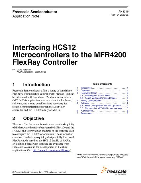
Interfacing HCS12 Microcontrollers to the MFR4200 FlexRay ...
Interfacing HCS12 Microcontrollers to the MFR4200 FlexRay ...
Interfacing HCS12 Microcontrollers to the MFR4200 FlexRay ...
Create successful ePaper yourself
Turn your PDF publications into a flip-book with our unique Google optimized e-Paper software.
Freescale Semiconduc<strong>to</strong>r<br />
Application Note<br />
1 Introduction<br />
Freescale Semiconduc<strong>to</strong>r offers a range of standalone<br />
<strong>FlexRay</strong> communication controllers (MFR4xxx) that can<br />
be interfaced with 16-bit and 32-bit microcontrollers<br />
(MCU). This application note describes <strong>the</strong> hardware,<br />
software, and timing considerations necessary for<br />
reliable communication between <strong>the</strong> <strong>MFR4200</strong><br />
controller and <strong>the</strong> <strong>HCS12</strong> family of MCUs.<br />
2 Objective<br />
The aim of <strong>the</strong> document is <strong>to</strong> demonstrate <strong>the</strong> simplicity<br />
of <strong>the</strong> hardware interface between <strong>the</strong> <strong>MFR4200</strong> and <strong>the</strong><br />
<strong>HCS12</strong>, and <strong>to</strong> provide an example of <strong>the</strong> software used<br />
<strong>to</strong> configure <strong>the</strong> <strong>HCS12</strong> for operation. The information<br />
contained can help you quickly design a fully functional<br />
<strong>FlexRay</strong> node based on <strong>the</strong> <strong>HCS12</strong> family of MCUs.<br />
Evaluation boards with software are available from<br />
Freescale <strong>to</strong> assist in <strong>the</strong> development of <strong>FlexRay</strong><br />
applications. (See http://www.freescale.com/flexray.)<br />
© Freescale Semiconduc<strong>to</strong>r, Inc., 2006. All rights reserved.<br />
Table of Contents<br />
AN3216<br />
Rev. 0, 2/2006<br />
<strong>Interfacing</strong> <strong>HCS12</strong><br />
<strong>Microcontrollers</strong> <strong>to</strong> <strong>the</strong> <strong>MFR4200</strong><br />
<strong>FlexRay</strong> Controller<br />
by: David Paterson<br />
MCD Applications, East Kilbride<br />
1 Introduction . . . . . . . . . . . . . . . . . . . . . . . . . . . . . . 1<br />
2 Objective . . . . . . . . . . . . . . . . . . . . . . . . . . . . . . . . 1<br />
3 Hardware Design . . . . . . . . . . . . . . . . . . . . . . . . . 2<br />
3.1 Selecting <strong>the</strong> <strong>HCS12</strong> Mode . . . . . . . . . . . . . . 2<br />
3.2 Paged Mode and Unpaged Mode . . . . . . . . . 2<br />
4 Timing Considerations . . . . . . . . . . . . . . . . . . . . . 6<br />
5 Software . . . . . . . . . . . . . . . . . . . . . . . . . . . . . . . . 7<br />
5.1 Mode Configuration and EBI Operation. . . . . 7<br />
5.2 Placement of <strong>MFR4200</strong> in Memory Map . . . . 8<br />
6 Conclusions . . . . . . . . . . . . . . . . . . . . . . . . . . . . . 8<br />
7 References . . . . . . . . . . . . . . . . . . . . . . . . . . . . . . 8<br />
Note: In this document, active-low signals are indicated<br />
by a “#” at <strong>the</strong> end of <strong>the</strong> signal name, e.g. “IRQn#”.
Hardware Design<br />
3 Hardware Design<br />
The <strong>MFR4200</strong> <strong>FlexRay</strong> controller has two separate controller host interfaces (CHI) on board — an <strong>HCS12</strong><br />
interface, for direct connection <strong>to</strong> Freescale’s <strong>HCS12</strong> family of microcontrollers, and an asynchronous<br />
memory interface (AMI) for asynchronous connection <strong>to</strong> all o<strong>the</strong>r microcontrollers. The <strong>HCS12</strong> interface<br />
clock signal, used <strong>to</strong> synchronize <strong>the</strong> data transfer, can run at a maximum rate of 8 MHz.<br />
Chip selection for <strong>the</strong> <strong>HCS12</strong> interface is generated internally using <strong>the</strong> following signals:<br />
• The expanded address signals XADDR[14:19] input values (<strong>HCS12</strong> is in <strong>the</strong> Paged or Unpaged<br />
mode of its External Bus Interface (EBI)) are compared with <strong>the</strong> logical 0’s.<br />
• The six most significant bits of <strong>the</strong> demultiplexed address bus, PAD[10:15], are compared with<br />
<strong>the</strong> pattern set up externally on <strong>the</strong> address chip select pins, ACS[0:5]. PAD10 is compared with<br />
ACS0, PAD11 with ACS1, …PAD15 with ACS5.<br />
NOTE<br />
The address decoding phase of a read/write operation is passed if all <strong>the</strong><br />
comparisons described above are passed.<br />
The devices can be connected <strong>to</strong>ge<strong>the</strong>r without additional glue logic, <strong>the</strong>reby simplifying <strong>the</strong> design and<br />
reducing <strong>the</strong> system cost.<br />
3.1 Selecting <strong>the</strong> <strong>HCS12</strong> Mode<br />
There are two modes of operation for <strong>the</strong> controller host interface (CHI), <strong>the</strong> AMI mode and <strong>the</strong> <strong>HCS12</strong><br />
mode. The <strong>HCS12</strong> mode is used <strong>to</strong> interface <strong>to</strong> <strong>the</strong> <strong>HCS12</strong> Family of microcontrollers.<br />
To select <strong>the</strong> <strong>HCS12</strong> mode, IF_SEL1 must be at <strong>the</strong> logic high level and IF_SEL0 must be at <strong>the</strong> logic low<br />
level. When using 3.3 V VDDIO , for example, IF_SEL1 must be pulled high using a 16 kΩ pullup resis<strong>to</strong>r,<br />
and IF_SEL0 must be pulled low using a 47 kΩ pulldown resis<strong>to</strong>r. (Similarly, at 3.3 V VDDIO , INT_CC#<br />
must be held high by a 16 kΩ pullup resis<strong>to</strong>r.)<br />
3.2 Paged Mode and Unpaged Mode<br />
There are two modes of operation that can be used when interfacing <strong>the</strong> <strong>HCS12</strong> and <strong>MFR4200</strong><br />
microcontrollers — paged and unpaged mode.<br />
Figure 1 and Figure 2 show block diagrams with all <strong>the</strong> EBI connections that are necessary for each mode<br />
of operation.<br />
Table 1 provides a description of each signal and pin that must be connected <strong>to</strong> interface <strong>the</strong> <strong>MFR4200</strong> <strong>to</strong><br />
a typical <strong>HCS12</strong> MCU, <strong>the</strong> MC9S12DP256B in a 112-pin LQFP package.<br />
2<br />
<strong>Interfacing</strong> <strong>HCS12</strong> <strong>Microcontrollers</strong> <strong>to</strong> <strong>the</strong> <strong>MFR4200</strong> <strong>FlexRay</strong> Controller, Rev. 0<br />
Freescale Semiconduc<strong>to</strong>r
<strong>HCS12</strong><br />
ADDR/DATA0<br />
…<br />
ADDR/DATA15<br />
EBI<br />
ECLK<br />
R/W#<br />
LSTRB<br />
XADDR14<br />
…<br />
XADDR19<br />
IRQn#<br />
V DDIO<br />
V DDIO<br />
…<br />
V DDIO<br />
V DDIO<br />
V DDIO<br />
TO THE PHY<br />
TO THE PHY<br />
PAD0<br />
… …<br />
… … … … …<br />
… … … …<br />
Figure 1. Connecting <strong>MFR4200</strong> <strong>to</strong> <strong>HCS12</strong> with Page Mode Support<br />
<strong>Interfacing</strong> <strong>HCS12</strong> <strong>Microcontrollers</strong> <strong>to</strong> <strong>the</strong> <strong>MFR4200</strong> <strong>FlexRay</strong> Controller, Rev. 0<br />
Hardware Design<br />
Freescale Semiconduc<strong>to</strong>r 3<br />
PAD15<br />
ACS5<br />
ACS4<br />
ACS3<br />
ACS0<br />
ECLK_CC<br />
RW_CC#<br />
LSTRB<br />
XADDR14<br />
…<br />
XADDR19<br />
INT_CC#<br />
<strong>MFR4200</strong><br />
IF_SEL1/TXD_BG1/TXD_485<br />
IF_SEL0/BGT/DBG2
Hardware Design<br />
4<br />
<strong>HCS12</strong><br />
EBI<br />
ADDR/DATA0<br />
…<br />
ADDR/DATA15<br />
ECLK<br />
R/W#<br />
LSTRB<br />
IRQn#<br />
… … … …<br />
V DDIO<br />
V DDIO<br />
… … … …<br />
V DDIO<br />
V DDIO<br />
TO THE PHY<br />
TO THE PHY<br />
PAD0<br />
PAD15<br />
ACS5<br />
ACS0<br />
ECLK_CC<br />
RW_CC#<br />
LSTRB<br />
XADDR[14:19]<br />
INT_CC#<br />
IF_SEL1/TXD_BG1/TXD_485<br />
IF_SEL0/BGT/DBG2<br />
Figure 2. Connecting <strong>MFR4200</strong> <strong>to</strong> <strong>HCS12</strong> with Unpaged Mode Support<br />
<strong>Interfacing</strong> <strong>HCS12</strong> <strong>Microcontrollers</strong> <strong>to</strong> <strong>the</strong> <strong>MFR4200</strong> <strong>FlexRay</strong> Controller, Rev. 0<br />
6<br />
…<br />
…<br />
<strong>MFR4200</strong><br />
Freescale Semiconduc<strong>to</strong>r
Table 1. Interface Signal Description<br />
<strong>HCS12</strong> <strong>to</strong> <strong>MFR4200</strong> Connection<br />
MC9S12DP256B (112-Pin LQFP) MFR200<br />
Signal Pin Signal Pin<br />
<strong>Interfacing</strong> <strong>HCS12</strong> <strong>Microcontrollers</strong> <strong>to</strong> <strong>the</strong> <strong>MFR4200</strong> <strong>FlexRay</strong> Controller, Rev. 0<br />
Hardware Design<br />
Comments<br />
ADDR0/DATA0/PB0 24 D15/PAD0 10 <strong>HCS12</strong> data/address bus (LSB)<br />
ADDR1/DATA1/PB1 25 D14/PAD1 7 <strong>HCS12</strong> data/address bus<br />
ADDR2/DATA2/PB2 26 D13/PAD2 6 <strong>HCS12</strong> data/address bus<br />
ADDR3/DATA3/PB3 27 D12/PAD3 5 <strong>HCS12</strong> data/address bus<br />
ADDR4/DATA4/PB4 28 D11/PAD4 4 <strong>HCS12</strong> data/address bus<br />
ADDR5/DATA5/PB5 29 D10/PAD5 3 <strong>HCS12</strong> data/address bus<br />
ADDR6/DATA6/PB6 30 D9/PAD6 2 <strong>HCS12</strong> data/address bus<br />
ADDR7/DATA7/PB7 31 D8/PAD7 62 <strong>HCS12</strong> data/address bus<br />
PA0/ADDR8/DATA8 57 D7/PAD8 61 <strong>HCS12</strong> data/address bus<br />
PA1/ADDR9/DATA9 58 D6/PAD9 58 <strong>HCS12</strong> data/address bus<br />
PA2/ADDR10/DATA10 59 D5/PAD10 57 <strong>HCS12</strong> data/address bus<br />
PA3/ADDR11/DATA11 60 D4/PAD11 56 <strong>HCS12</strong> data/address bus<br />
PA4/ADDR12/DATA12 61 D3/PAD12 55 <strong>HCS12</strong> data/address bus<br />
PA5/ADDR13/DATA13 62 D2/PAD13 51 <strong>HCS12</strong> data/address bus<br />
PA6/ADDR14/DATA14 63 D1/PAD14 40 <strong>HCS12</strong> data/address bus<br />
PA7/ADDR15/DATA15 64 D0/PAD15 39 <strong>HCS12</strong> data/address bus<br />
XADDR14/PK0 8 A6/XADDR14 17 Extended addresses (page mode)<br />
XADDR15/PK1 7 A5/XADDR15 15 Extended addresses (page mode)<br />
XADDR16/PK2 6 A4/XADDR16 14 Extended addresses (page mode)<br />
XADDR17/PK3 5 A3/XADDR17 13 Extended addresses (page mode)<br />
XADDR18/PK4 20 A2/XADDR18 12 Extended addresses (page mode)<br />
XADDR19/PK5 19 A1/XADDR19 11 Extended addresses (page mode)<br />
ECLK/PE4 39 ECLK_CC 52 <strong>HCS12</strong> clock input<br />
R/W#/PE2 54 WE#/RW_CC# 30 <strong>HCS12</strong> read/write select signal<br />
LSTRB/TAGL0/PE3 53 CE#/LSTRB 29 <strong>HCS12</strong> low-byte strobe signal<br />
GPIO (or PU/PD) ACS0–ACS5 18, 21, 22,<br />
27, 28, 34<br />
<strong>HCS12</strong> address select inputs<br />
GPIO RESET# 16 Hardware reset input<br />
PE1/IRQ# 55 INT_CC# 64 Controller interrupt output<br />
BGT/DBG2/IF_SEL0 32 Host interface selection =<br />
LOW (<strong>HCS12</strong> mode)<br />
TXD_BG1/TXD1_485/IF_SEL1 41 Host interface selection =<br />
HIGH (<strong>HCS12</strong> mode)<br />
Freescale Semiconduc<strong>to</strong>r 5
Timing Considerations<br />
4 Timing Considerations<br />
For <strong>the</strong> <strong>HCS12</strong> and <strong>the</strong> <strong>MFR4200</strong> communication controller <strong>to</strong> communicate reliably, <strong>the</strong> timing between<br />
<strong>the</strong> <strong>HCS12</strong> and <strong>the</strong> <strong>MFR4200</strong> must be matched. There is a requirement for <strong>the</strong> addition of stretch cycles 1<br />
<strong>to</strong> match <strong>the</strong> timing characteristics. Refer <strong>to</strong> Section 8, “<strong>MFR4200</strong> <strong>HCS12</strong> Timing Specifications” for<br />
specific timing diagrams. A minimum of one stretch cycle must be inserted when running with an 8 MHz<br />
external clock. Table 3 summarizes <strong>the</strong> read and write timing for one stretch cycle, which is required for<br />
successful operation. The number of stretch cycles that can be added is controlled in <strong>the</strong> Miscellaneous<br />
System Control Register (MISC). Refer <strong>to</strong> <strong>the</strong> Module Mapping Control (MMC) section of <strong>the</strong> user<br />
manual. The available options are shown in Table 2.<br />
1. When accessing on-chip peripherals and memories, <strong>the</strong> <strong>HCS12</strong> performs 8-bit and 16-bit core accesses in a single cycle.<br />
However, when <strong>the</strong> core accesses locations on <strong>the</strong> external bus using <strong>the</strong> expanded modes, <strong>the</strong> accesses are stretched and<br />
take more than a single cycle <strong>to</strong> complete. The minimum amount of stretching is one additional bus cycle, but can be increased.<br />
See Table 2 for details.<br />
6<br />
Table 2. Stretch Cycle Selection<br />
External Access Stretch Bit Definition<br />
EXSTR[1:0]<br />
Number of E Clocks<br />
Stretched<br />
00 0 cycles<br />
01 1 cycle<br />
10 2 cycles<br />
11 3 cycles<br />
Table 3. <strong>HCS12</strong> <strong>to</strong> <strong>MFR4200</strong> Timing Parameters with One Stretch Cycle<br />
Num Rating<br />
Specified 1 Wait<br />
Min Max Measured Comment<br />
1 Pulse width, ECLK low 25 — 685 PASS<br />
2 Pulse width, ECLK high 114 — 190 PASS<br />
3, 11 Address valid time <strong>to</strong> E rise 11 — 54 PASS<br />
4 Write data delay time — 7 4 PASS<br />
5 ECLK rise <strong>to</strong> write data invalid 71 — 184 PASS<br />
6 (4) Write data hold time 2 — 2 PASS<br />
7 RW delay time — 7 0 PASS<br />
8 RW valid time <strong>to</strong> ECLK rise 14 — 56 PASS<br />
9 RW hold time 2 — 2 PASS<br />
10 Data hold <strong>to</strong> address 2 — 54 PASS<br />
12 Multiplexed address hold time 2 — 64 PASS<br />
13 ECLK high access time<br />
(ECLK high <strong>to</strong> read data valid)<br />
50 75 70 PASS<br />
14 Read data setup time 13 — 120 PASS<br />
15 Read data hold time 0 — 97 PASS<br />
<strong>Interfacing</strong> <strong>HCS12</strong> <strong>Microcontrollers</strong> <strong>to</strong> <strong>the</strong> <strong>MFR4200</strong> <strong>FlexRay</strong> Controller, Rev. 0<br />
Freescale Semiconduc<strong>to</strong>r
5 Software<br />
<strong>Interfacing</strong> <strong>HCS12</strong> <strong>Microcontrollers</strong> <strong>to</strong> <strong>the</strong> <strong>MFR4200</strong> <strong>FlexRay</strong> Controller, Rev. 0<br />
Software<br />
The software setup is concerned mainly with selection of <strong>the</strong> correct MCU operating mode, configuration<br />
of <strong>the</strong> <strong>HCS12</strong> for communication with <strong>the</strong> <strong>MFR4200</strong>, and linking in<strong>to</strong> <strong>the</strong> correct area of <strong>the</strong> memory map.<br />
5.1 Mode Configuration and EBI Operation<br />
As already stated, <strong>the</strong> <strong>HCS12</strong> must be configured in<strong>to</strong> normal expanded mode <strong>to</strong> enable <strong>the</strong> bus interface.<br />
In this mode, ports A and B are configured for <strong>the</strong> data/address bus, and port E is configured for <strong>the</strong> control<br />
signals. During initialization, <strong>the</strong> EBI is configured, and <strong>the</strong> mode is set <strong>to</strong> normal expanded wide (BDM<br />
allowed) mode by writing MODC = 1, MODB = 1, and MODA = 1 in <strong>the</strong> MODE register. The EBI must<br />
be initialized <strong>to</strong> use <strong>the</strong> correct chip select and <strong>to</strong> select <strong>the</strong> correct number of stretch cycles. See Section 4,<br />
“Timing Considerations” for specific details.<br />
Figure 3 shows <strong>the</strong> steps required <strong>to</strong> configure <strong>the</strong> <strong>HCS12</strong> MCU for communication with <strong>the</strong> <strong>MFR4200</strong><br />
controller.<br />
Set up ports<br />
Set up ACS signals<br />
(ACS[5:0] = 100000)<br />
Enable <strong>the</strong> EBI<br />
and control signals<br />
Enable stretch clock<br />
and number of stretch<br />
cycles<br />
Set normal expanded<br />
wide mode<br />
Figure 3. Initialization Flow Diagram<br />
Freescale Semiconduc<strong>to</strong>r 7
Conclusions<br />
5.2 Placement of <strong>MFR4200</strong> in Memory Map<br />
The global address, associated with each chip select signal, is generated by a concatenation of <strong>the</strong> <strong>HCS12</strong><br />
local address [15:0] with <strong>the</strong> global page index register, where <strong>the</strong> page index bits are effectively used <strong>to</strong><br />
select which of <strong>the</strong> 128 x 64 Kbyte pages is <strong>to</strong> be accessed. In order <strong>to</strong> access global addressing, specific<br />
global instructions must be used.<br />
For example:<br />
GLDD — Load double accumula<strong>to</strong>r D (A:B) from global memory.<br />
GSTAA — S<strong>to</strong>re <strong>the</strong> contents of accumula<strong>to</strong>r A in<strong>to</strong> global memory<br />
In Metrowerks CodeWarrior, <strong>the</strong> FAR qualifier is used <strong>to</strong> tell <strong>the</strong> compiler <strong>to</strong> use <strong>the</strong> global instructions<br />
included in <strong>the</strong> <strong>HCS12</strong> CPU. An example of how <strong>to</strong> place <strong>the</strong> <strong>MFR4200</strong> registers in<strong>to</strong> <strong>the</strong> memory map is<br />
shown below.<br />
Example:<br />
8<br />
#define BASE_ADDRESS 0x8000<br />
#define MNR (*(volatile unsigned int* far)(0x000 + BASE_ADDRESS))<br />
#define MVR (*(volatile unsigned int* far)(0x002 + BASE_ADDRESS))<br />
#define MCR0 (*(volatile unsigned int* far)(0x004 + BASE_ADDRESS))<br />
In this option, <strong>the</strong> placement of <strong>the</strong> memory map can be changed by modifying <strong>the</strong> BASE_ADDRESS.<br />
The selected BASE_ADDRESS of 8000 is in <strong>the</strong> CS2# address range. 1<br />
6 Conclusions<br />
The <strong>FlexRay</strong> controller can be connected <strong>to</strong> <strong>the</strong> <strong>HCS12</strong> Family of MCUs, with a maximum interface clock<br />
frequency (<strong>to</strong> synchronize data transfer) of 8 MHz.<br />
Due <strong>to</strong> this specific interface between <strong>the</strong> <strong>HCS12</strong> microcontrollers and <strong>MFR4200</strong> <strong>FlexRay</strong> controller, no<br />
glue logic required. Software configuration is also straightforward, <strong>the</strong> peripheral being simply<br />
memory-mapped in<strong>to</strong> <strong>the</strong> global address space.<br />
7 References<br />
1. MC9S12DP256B Data Sheet<br />
2. <strong>MFR4200</strong> <strong>FlexRay</strong> Communication Controller Data Sheet<br />
These documents are available on <strong>the</strong> Freescale Semiconduc<strong>to</strong>r web site at http://www.freescale.com.<br />
More information on <strong>FlexRay</strong> and <strong>FlexRay</strong> products can be found at http://www.freescale.com/flexray<br />
1. Many alternative methods of defining <strong>the</strong> <strong>MFR4200</strong> register exist.<br />
<strong>Interfacing</strong> <strong>HCS12</strong> <strong>Microcontrollers</strong> <strong>to</strong> <strong>the</strong> <strong>MFR4200</strong> <strong>FlexRay</strong> Controller, Rev. 0<br />
Freescale Semiconduc<strong>to</strong>r
<strong>Interfacing</strong> <strong>HCS12</strong> <strong>Microcontrollers</strong> <strong>to</strong> <strong>the</strong> <strong>MFR4200</strong> <strong>FlexRay</strong> Controller, Rev. 0<br />
References<br />
Freescale Semiconduc<strong>to</strong>r 9
How <strong>to</strong> Reach Us:<br />
Home Page:<br />
www.freescale.com<br />
E-mail:<br />
support@freescale.com<br />
USA/Europe or Locations Not Listed:<br />
Freescale Semiconduc<strong>to</strong>r<br />
Technical Information Center, CH370<br />
1300 N. Alma School Road<br />
Chandler, Arizona 85224<br />
+1-800-521-6274 or +1-480-768-2130<br />
support@freescale.com<br />
Europe, Middle East, and Africa:<br />
Freescale Halbleiter Deutschland GmbH<br />
Technical Information Center<br />
Schatzbogen 7<br />
81829 Muenchen, Germany<br />
+44 1296 380 456 (English)<br />
+46 8 52200080 (English)<br />
+49 89 92103 559 (German)<br />
+33 1 69 35 48 48 (French)<br />
support@freescale.com<br />
Japan:<br />
Freescale Semiconduc<strong>to</strong>r Japan Ltd.<br />
Headquarters<br />
ARCO Tower 15F<br />
1-8-1, Shimo-Meguro, Meguro-ku,<br />
Tokyo 153-0064<br />
Japan<br />
0120 191014 or +81 3 5437 9125<br />
support.japan@freescale.com<br />
Asia/Pacific:<br />
Freescale Semiconduc<strong>to</strong>r Hong Kong Ltd.<br />
Technical Information Center<br />
2 Dai King Street<br />
Tai Po Industrial Estate<br />
Tai Po, N.T., Hong Kong<br />
+800 2666 8080<br />
support.asia@freescale.com<br />
For Literature Requests Only:<br />
Freescale Semiconduc<strong>to</strong>r Literature Distribution Center<br />
P.O. Box 5405<br />
Denver, Colorado 80217<br />
1-800-441-2447 or 303-675-2140<br />
Fax: 303-675-2150<br />
LDCForFreescaleSemiconduc<strong>to</strong>r@hibbertgroup.com<br />
AN3216<br />
Rev. 0, 2/2006<br />
Information in this document is provided solely <strong>to</strong> enable system and software<br />
implementers <strong>to</strong> use Freescale Semiconduc<strong>to</strong>r products. There are no express or<br />
implied copyright licenses granted hereunder <strong>to</strong> design or fabricate any integrated<br />
circuits or integrated circuits based on <strong>the</strong> information in this document.<br />
Freescale Semiconduc<strong>to</strong>r reserves <strong>the</strong> right <strong>to</strong> make changes without fur<strong>the</strong>r notice <strong>to</strong><br />
any products herein. Freescale Semiconduc<strong>to</strong>r makes no warranty, representation or<br />
guarantee regarding <strong>the</strong> suitability of its products for any particular purpose, nor does<br />
Freescale Semiconduc<strong>to</strong>r assume any liability arising out of <strong>the</strong> application or use of any<br />
product or circuit, and specifically disclaims any and all liability, including without<br />
limitation consequential or incidental damages. “Typical” parameters that may be<br />
provided in Freescale Semiconduc<strong>to</strong>r data sheets and/or specifications can and do vary<br />
in different applications and actual performance may vary over time. All operating<br />
parameters, including “Typicals”, must be validated for each cus<strong>to</strong>mer application by<br />
cus<strong>to</strong>mer’s technical experts. Freescale Semiconduc<strong>to</strong>r does not convey any license<br />
under its patent rights nor <strong>the</strong> rights of o<strong>the</strong>rs. Freescale Semiconduc<strong>to</strong>r products are<br />
not designed, intended, or authorized for use as components in systems intended for<br />
surgical implant in<strong>to</strong> <strong>the</strong> body, or o<strong>the</strong>r applications intended <strong>to</strong> support or sustain life,<br />
or for any o<strong>the</strong>r application in which <strong>the</strong> failure of <strong>the</strong> Freescale Semiconduc<strong>to</strong>r product<br />
could create a situation where personal injury or death may occur. Should Buyer<br />
purchase or use Freescale Semiconduc<strong>to</strong>r products for any such unintended or<br />
unauthorized application, Buyer shall indemnify and hold Freescale Semiconduc<strong>to</strong>r and<br />
its officers, employees, subsidiaries, affiliates, and distribu<strong>to</strong>rs harmless against all<br />
claims, costs, damages, and expenses, and reasonable at<strong>to</strong>rney fees arising out of,<br />
directly or indirectly, any claim of personal injury or death associated with such<br />
unintended or unauthorized use, even if such claim alleges that Freescale<br />
Semiconduc<strong>to</strong>r was negligent regarding <strong>the</strong> design or manufacture of <strong>the</strong> part.<br />
Freescale and <strong>the</strong> Freescale logo are trademarks of Freescale Semiconduc<strong>to</strong>r, Inc.<br />
All o<strong>the</strong>r product or service names are <strong>the</strong> property of <strong>the</strong>ir respective owners.<br />
© Freescale Semiconduc<strong>to</strong>r, Inc. 2006. All rights reserved.


